JP2006030317A - Organic el display device - Google Patents
Organic el display deviceDownload PDFInfo
- Publication number
- JP2006030317A JP2006030317AJP2004205256AJP2004205256AJP2006030317AJP 2006030317 AJP2006030317 AJP 2006030317AJP 2004205256 AJP2004205256 AJP 2004205256AJP 2004205256 AJP2004205256 AJP 2004205256AJP 2006030317 AJP2006030317 AJP 2006030317A
- Authority
- JP
- Japan
- Prior art keywords
- organic
- power supply
- switching transistor
- light
- drain
- Prior art date
- Legal status (The legal status is an assumption and is not a legal conclusion. Google has not performed a legal analysis and makes no representation as to the accuracy of the status listed.)
- Withdrawn
Links
- 239000003990capacitorSubstances0.000claimsdescription47
- 239000010408filmSubstances0.000claimsdescription27
- 239000004065semiconductorSubstances0.000claimsdescription23
- 239000000758substrateSubstances0.000claimsdescription23
- 230000035945sensitivityEffects0.000claimsdescription19
- 239000012535impuritySubstances0.000claimsdescription12
- 239000011159matrix materialSubstances0.000claimsdescription9
- 239000010409thin filmSubstances0.000claimsdescription5
- 239000010410layerSubstances0.000description42
- 238000010586diagramMethods0.000description29
- 238000001514detection methodMethods0.000description15
- 229920006395saturated elastomerPolymers0.000description7
- 230000007423decreaseEffects0.000description5
- 238000005401electroluminescenceMethods0.000description5
- 230000005525hole transportEffects0.000description5
- 239000011229interlayerSubstances0.000description5
- 229910004298SiO 2Inorganic materials0.000description4
- 239000011521glassSubstances0.000description4
- 230000000903blocking effectEffects0.000description3
- 230000005684electric fieldEffects0.000description3
- 238000010030laminatingMethods0.000description3
- 238000000034methodMethods0.000description3
- 238000012935AveragingMethods0.000description2
- 229910052782aluminiumInorganic materials0.000description2
- XAGFODPZIPBFFR-UHFFFAOYSA-NaluminiumChemical compound[Al]XAGFODPZIPBFFR-UHFFFAOYSA-N0.000description2
- 238000013459approachMethods0.000description2
- 239000011651chromiumSubstances0.000description2
- 230000003111delayed effectEffects0.000description2
- AMGQUBHHOARCQH-UHFFFAOYSA-Nindium;oxotinChemical compound[In].[Sn]=OAMGQUBHHOARCQH-UHFFFAOYSA-N0.000description2
- 229910052751metalInorganic materials0.000description2
- 239000002184metalSubstances0.000description2
- VYZAMTAEIAYCRO-UHFFFAOYSA-NChromiumChemical compound[Cr]VYZAMTAEIAYCRO-UHFFFAOYSA-N0.000description1
- 229910000846In alloyInorganic materials0.000description1
- FYYHWMGAXLPEAU-UHFFFAOYSA-NMagnesiumChemical compound[Mg]FYYHWMGAXLPEAU-UHFFFAOYSA-N0.000description1
- 229910000861Mg alloyInorganic materials0.000description1
- ZOKXTWBITQBERF-UHFFFAOYSA-NMolybdenumChemical compound[Mo]ZOKXTWBITQBERF-UHFFFAOYSA-N0.000description1
- VYPSYNLAJGMNEJ-UHFFFAOYSA-NSilicium dioxideChemical compoundO=[Si]=OVYPSYNLAJGMNEJ-UHFFFAOYSA-N0.000description1
- 229910021417amorphous siliconInorganic materials0.000description1
- 238000006243chemical reactionMethods0.000description1
- 229910052804chromiumInorganic materials0.000description1
- 230000009849deactivationEffects0.000description1
- 238000009792diffusion processMethods0.000description1
- 238000007599dischargingMethods0.000description1
- 238000000605extractionMethods0.000description1
- 230000010354integrationEffects0.000description1
- 238000005224laser annealingMethods0.000description1
- 239000004973liquid crystal related substanceSubstances0.000description1
- 239000011777magnesiumSubstances0.000description1
- 238000004519manufacturing processMethods0.000description1
- 229910052750molybdenumInorganic materials0.000description1
- 239000011733molybdenumSubstances0.000description1
- 229910021420polycrystalline siliconInorganic materials0.000description1
- 229920005591polysiliconPolymers0.000description1
- 230000005855radiationEffects0.000description1
- 239000003870refractory metalSubstances0.000description1
Images


Classifications
- G—PHYSICS
- G09—EDUCATION; CRYPTOGRAPHY; DISPLAY; ADVERTISING; SEALS
- G09G—ARRANGEMENTS OR CIRCUITS FOR CONTROL OF INDICATING DEVICES USING STATIC MEANS TO PRESENT VARIABLE INFORMATION
- G09G3/00—Control arrangements or circuits, of interest only in connection with visual indicators other than cathode-ray tubes
- G09G3/20—Control arrangements or circuits, of interest only in connection with visual indicators other than cathode-ray tubes for presentation of an assembly of a number of characters, e.g. a page, by composing the assembly by combination of individual elements arranged in a matrix no fixed position being assigned to or needed to be assigned to the individual characters or partial characters
- G09G3/22—Control arrangements or circuits, of interest only in connection with visual indicators other than cathode-ray tubes for presentation of an assembly of a number of characters, e.g. a page, by composing the assembly by combination of individual elements arranged in a matrix no fixed position being assigned to or needed to be assigned to the individual characters or partial characters using controlled light sources
- G09G3/30—Control arrangements or circuits, of interest only in connection with visual indicators other than cathode-ray tubes for presentation of an assembly of a number of characters, e.g. a page, by composing the assembly by combination of individual elements arranged in a matrix no fixed position being assigned to or needed to be assigned to the individual characters or partial characters using controlled light sources using electroluminescent panels
- G09G3/32—Control arrangements or circuits, of interest only in connection with visual indicators other than cathode-ray tubes for presentation of an assembly of a number of characters, e.g. a page, by composing the assembly by combination of individual elements arranged in a matrix no fixed position being assigned to or needed to be assigned to the individual characters or partial characters using controlled light sources using electroluminescent panels semiconductive, e.g. using light-emitting diodes [LED]
- G09G3/3208—Control arrangements or circuits, of interest only in connection with visual indicators other than cathode-ray tubes for presentation of an assembly of a number of characters, e.g. a page, by composing the assembly by combination of individual elements arranged in a matrix no fixed position being assigned to or needed to be assigned to the individual characters or partial characters using controlled light sources using electroluminescent panels semiconductive, e.g. using light-emitting diodes [LED] organic, e.g. using organic light-emitting diodes [OLED]
- G09G3/3225—Control arrangements or circuits, of interest only in connection with visual indicators other than cathode-ray tubes for presentation of an assembly of a number of characters, e.g. a page, by composing the assembly by combination of individual elements arranged in a matrix no fixed position being assigned to or needed to be assigned to the individual characters or partial characters using controlled light sources using electroluminescent panels semiconductive, e.g. using light-emitting diodes [LED] organic, e.g. using organic light-emitting diodes [OLED] using an active matrix
- G09G3/3233—Control arrangements or circuits, of interest only in connection with visual indicators other than cathode-ray tubes for presentation of an assembly of a number of characters, e.g. a page, by composing the assembly by combination of individual elements arranged in a matrix no fixed position being assigned to or needed to be assigned to the individual characters or partial characters using controlled light sources using electroluminescent panels semiconductive, e.g. using light-emitting diodes [LED] organic, e.g. using organic light-emitting diodes [OLED] using an active matrix with pixel circuitry controlling the current through the light-emitting element
- G—PHYSICS
- G09—EDUCATION; CRYPTOGRAPHY; DISPLAY; ADVERTISING; SEALS
- G09G—ARRANGEMENTS OR CIRCUITS FOR CONTROL OF INDICATING DEVICES USING STATIC MEANS TO PRESENT VARIABLE INFORMATION
- G09G3/00—Control arrangements or circuits, of interest only in connection with visual indicators other than cathode-ray tubes
- G09G3/20—Control arrangements or circuits, of interest only in connection with visual indicators other than cathode-ray tubes for presentation of an assembly of a number of characters, e.g. a page, by composing the assembly by combination of individual elements arranged in a matrix no fixed position being assigned to or needed to be assigned to the individual characters or partial characters
- G09G3/22—Control arrangements or circuits, of interest only in connection with visual indicators other than cathode-ray tubes for presentation of an assembly of a number of characters, e.g. a page, by composing the assembly by combination of individual elements arranged in a matrix no fixed position being assigned to or needed to be assigned to the individual characters or partial characters using controlled light sources
- G09G3/30—Control arrangements or circuits, of interest only in connection with visual indicators other than cathode-ray tubes for presentation of an assembly of a number of characters, e.g. a page, by composing the assembly by combination of individual elements arranged in a matrix no fixed position being assigned to or needed to be assigned to the individual characters or partial characters using controlled light sources using electroluminescent panels
- G09G3/32—Control arrangements or circuits, of interest only in connection with visual indicators other than cathode-ray tubes for presentation of an assembly of a number of characters, e.g. a page, by composing the assembly by combination of individual elements arranged in a matrix no fixed position being assigned to or needed to be assigned to the individual characters or partial characters using controlled light sources using electroluminescent panels semiconductive, e.g. using light-emitting diodes [LED]
- G09G3/3208—Control arrangements or circuits, of interest only in connection with visual indicators other than cathode-ray tubes for presentation of an assembly of a number of characters, e.g. a page, by composing the assembly by combination of individual elements arranged in a matrix no fixed position being assigned to or needed to be assigned to the individual characters or partial characters using controlled light sources using electroluminescent panels semiconductive, e.g. using light-emitting diodes [LED] organic, e.g. using organic light-emitting diodes [OLED]
- G09G3/3275—Details of drivers for data electrodes
- G09G3/3291—Details of drivers for data electrodes in which the data driver supplies a variable data voltage for setting the current through, or the voltage across, the light-emitting elements
- H—ELECTRICITY
- H05—ELECTRIC TECHNIQUES NOT OTHERWISE PROVIDED FOR
- H05B—ELECTRIC HEATING; ELECTRIC LIGHT SOURCES NOT OTHERWISE PROVIDED FOR; CIRCUIT ARRANGEMENTS FOR ELECTRIC LIGHT SOURCES, IN GENERAL
- H05B33/00—Electroluminescent light sources
- H05B33/12—Light sources with substantially two-dimensional radiating surfaces
- H05B33/26—Light sources with substantially two-dimensional radiating surfaces characterised by the composition or arrangement of the conductive material used as an electrode
- H—ELECTRICITY
- H10—SEMICONDUCTOR DEVICES; ELECTRIC SOLID-STATE DEVICES NOT OTHERWISE PROVIDED FOR
- H10K—ORGANIC ELECTRIC SOLID-STATE DEVICES
- H10K59/00—Integrated devices, or assemblies of multiple devices, comprising at least one organic light-emitting element covered by group H10K50/00
- H10K59/10—OLED displays
- H10K59/12—Active-matrix OLED [AMOLED] displays
- H10K59/13—Active-matrix OLED [AMOLED] displays comprising photosensors that control luminance
- G—PHYSICS
- G09—EDUCATION; CRYPTOGRAPHY; DISPLAY; ADVERTISING; SEALS
- G09G—ARRANGEMENTS OR CIRCUITS FOR CONTROL OF INDICATING DEVICES USING STATIC MEANS TO PRESENT VARIABLE INFORMATION
- G09G2300/00—Aspects of the constitution of display devices
- G09G2300/08—Active matrix structure, i.e. with use of active elements, inclusive of non-linear two terminal elements, in the pixels together with light emitting or modulating elements
- G09G2300/0809—Several active elements per pixel in active matrix panels
- G09G2300/0842—Several active elements per pixel in active matrix panels forming a memory circuit, e.g. a dynamic memory with one capacitor
- G09G2300/0852—Several active elements per pixel in active matrix panels forming a memory circuit, e.g. a dynamic memory with one capacitor being a dynamic memory with more than one capacitor
- G—PHYSICS
- G09—EDUCATION; CRYPTOGRAPHY; DISPLAY; ADVERTISING; SEALS
- G09G—ARRANGEMENTS OR CIRCUITS FOR CONTROL OF INDICATING DEVICES USING STATIC MEANS TO PRESENT VARIABLE INFORMATION
- G09G2320/00—Control of display operating conditions
- G09G2320/02—Improving the quality of display appearance
- G09G2320/0271—Adjustment of the gradation levels within the range of the gradation scale, e.g. by redistribution or clipping
- G09G2320/0276—Adjustment of the gradation levels within the range of the gradation scale, e.g. by redistribution or clipping for the purpose of adaptation to the characteristics of a display device, i.e. gamma correction
- G—PHYSICS
- G09—EDUCATION; CRYPTOGRAPHY; DISPLAY; ADVERTISING; SEALS
- G09G—ARRANGEMENTS OR CIRCUITS FOR CONTROL OF INDICATING DEVICES USING STATIC MEANS TO PRESENT VARIABLE INFORMATION
- G09G2320/00—Control of display operating conditions
- G09G2320/02—Improving the quality of display appearance
- G09G2320/029—Improving the quality of display appearance by monitoring one or more pixels in the display panel, e.g. by monitoring a fixed reference pixel
- G09G2320/0295—Improving the quality of display appearance by monitoring one or more pixels in the display panel, e.g. by monitoring a fixed reference pixel by monitoring each display pixel
- G—PHYSICS
- G09—EDUCATION; CRYPTOGRAPHY; DISPLAY; ADVERTISING; SEALS
- G09G—ARRANGEMENTS OR CIRCUITS FOR CONTROL OF INDICATING DEVICES USING STATIC MEANS TO PRESENT VARIABLE INFORMATION
- G09G2320/00—Control of display operating conditions
- G09G2320/04—Maintaining the quality of display appearance
- G09G2320/043—Preventing or counteracting the effects of ageing
- G09G2320/045—Compensation of drifts in the characteristics of light emitting or modulating elements
- G—PHYSICS
- G09—EDUCATION; CRYPTOGRAPHY; DISPLAY; ADVERTISING; SEALS
- G09G—ARRANGEMENTS OR CIRCUITS FOR CONTROL OF INDICATING DEVICES USING STATIC MEANS TO PRESENT VARIABLE INFORMATION
- G09G2320/00—Control of display operating conditions
- G09G2320/06—Adjustment of display parameters
- G09G2320/0666—Adjustment of display parameters for control of colour parameters, e.g. colour temperature
- G—PHYSICS
- G09—EDUCATION; CRYPTOGRAPHY; DISPLAY; ADVERTISING; SEALS
- G09G—ARRANGEMENTS OR CIRCUITS FOR CONTROL OF INDICATING DEVICES USING STATIC MEANS TO PRESENT VARIABLE INFORMATION
- G09G2330/00—Aspects of power supply; Aspects of display protection and defect management
- G09G2330/02—Details of power systems and of start or stop of display operation
- G09G2330/021—Power management, e.g. power saving
- G—PHYSICS
- G09—EDUCATION; CRYPTOGRAPHY; DISPLAY; ADVERTISING; SEALS
- G09G—ARRANGEMENTS OR CIRCUITS FOR CONTROL OF INDICATING DEVICES USING STATIC MEANS TO PRESENT VARIABLE INFORMATION
- G09G2360/00—Aspects of the architecture of display systems
- G09G2360/14—Detecting light within display terminals, e.g. using a single or a plurality of photosensors
- G09G2360/145—Detecting light within display terminals, e.g. using a single or a plurality of photosensors the light originating from the display screen
- G09G2360/147—Detecting light within display terminals, e.g. using a single or a plurality of photosensors the light originating from the display screen the originated light output being determined for each pixel
- G09G2360/148—Detecting light within display terminals, e.g. using a single or a plurality of photosensors the light originating from the display screen the originated light output being determined for each pixel the light being detected by light detection means within each pixel
Landscapes
- Engineering & Computer Science (AREA)
- Physics & Mathematics (AREA)
- Computer Hardware Design (AREA)
- General Physics & Mathematics (AREA)
- Theoretical Computer Science (AREA)
- Microelectronics & Electronic Packaging (AREA)
- Electroluminescent Light Sources (AREA)
- Control Of El Displays (AREA)
- Control Of Indicators Other Than Cathode Ray Tubes (AREA)
- Devices For Indicating Variable Information By Combining Individual Elements (AREA)
- Thin Film Transistor (AREA)
Abstract
Description
Translated fromJapanese本発明は、有機EL表示装置に係り、特に表示部の画素毎の輝度ムラを調整可能とした有機EL表示装置に関する。 The present invention relates to an organic EL display device, and more particularly to an organic EL display device capable of adjusting luminance unevenness for each pixel of a display unit.
有機EL素子は、自ら発光するため液晶表示装置で必要なバックライトが要らず薄型化に最適であると共に、視野角にも制限が無いため、次世代の表示装置としてその実用化が大きく期待されている。 Since organic EL elements emit light themselves, they do not require a backlight necessary for liquid crystal display devices and are optimal for thinning, and there are no restrictions on viewing angles. ing.
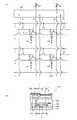
ところで、有機EL表示装置の駆動方式としては、単純マトリクスのパッシブ型とTFTを使用するアクティブ型の2種類があり、アクティブ型においては一般に図15(A)に示す回路構成が用いられている。図15(A)は有機EL表示装置の表示部の回路概要図であり、図15(B)は1画素の一部断面図である。 By the way, there are two types of driving methods for the organic EL display device, that is, a passive type using a simple matrix and an active type using TFTs. In the active type, the circuit configuration shown in FIG. 15A is generally used. FIG. 15A is a circuit schematic diagram of a display portion of an organic EL display device, and FIG. 15B is a partial cross-sectional view of one pixel.
図15(A)のごとく行方向に延びる複数のゲート線1が配置され、これに交差するように列方向に複数のドレイン線2及び第1電源線3が配置されている。 As shown in FIG. 15A, a plurality of
ゲート線1とドレイン線2とのそれぞれの交点には選択TFT4が接続されている。選択TFT4のゲートはゲート線1に接続され、選択TFT4のドレインがドレイン線2に接続されている。選択TFT4のソースは保持コンデンサ5と駆動TFT6のゲートに接続されている。 A selection TFT 4 is connected to each intersection of the
駆動TFT6のドレインは、第1電源線3に接続され、ソースは有機EL素子7の陽極に接続されている。保持コンデンサ5の対極は、列方向に延在する第2電源線9と接続する。 The drain of the driving TFT 6 is connected to the first
ゲート線1は図示しないVスキャナに接続され、ゲート線1には、Vスキャナによって順次ゲート信号が印加される。ゲート信号はオンもしくはオフの2値の信号で、オンの時は正の所定電圧、オフの時は0Vとなる。Vスキャナは、複数接続されるゲート線1のうち、選択された所定のゲート線のゲート信号をオンとする。ゲート信号がオンとなると、そのゲート線1に接続された全ての選択TFT4がオンとなり、選択TFT4を介してドレイン線2と駆動TFT6のゲートが接続される。 The
ドレイン線2にはHスキャナ22から表示する映像に応じて決定されるデータ信号が出力されており、データ信号は駆動TFT6のゲートに入力されるとともに、保持コンデンサ5に充電される。 A data signal determined according to an image displayed from the
駆動TFT6は、データ信号の大きさに応じた導電率で第1電源線3と有機EL素子7とを接続する。この結果、データ信号に応じた電流が駆動TFT6を介して第1電源線3から有機EL素子7に供給され、データ信号に応じた輝度で有機EL素子7が発光する。 The driving TFT 6 connects the first
保持コンデンサ5は、第2電源線9もしくは第1電源線3など他の電極との間で静電容量を形成しており、一定時間データ信号を蓄積することができる。 The
データ信号は、Vスキャナが他のゲート線1を選択し、そのゲート線1が非選択となって選択TFT4がオフした後も、保持コンデンサ5によって1垂直走査期間の間保持され、その間、駆動TFT6は前記導電率を保持し、有機EL素子7はその輝度で発光を続けることができる。 The data signal is held for one vertical scanning period by the
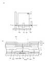
図15(B)の如く、有機EL表示装置の画素130は、ガラス基板151上に複数の駆動TFT6が配置されている。駆動TFT6はゲート電極6Gが、層間絶縁膜152を介してソース6S、チャネル6C、ドレイン6Dと対向する構造であり、ここに示す例では、チャネル6Cよりもゲート電極6Gが下にあるボトムゲート構造である。 As shown in FIG. 15B, the
駆動TFT6上に層間絶縁膜153が形成され、その上にドレイン線2及び第1電源線3が配置されている。第1電源線3は、駆動TFT6のドレイン6Dにコンタクトを介して接続されている。それらの上に、平坦化絶縁膜154が形成されており、平坦化絶縁膜154の上には画素毎に有機EL素子7が配置されている。 An
有機EL素子7は、ITO(indium tin oxide)等の透明電極よりなる陽極155、ホール輸送層156、発光層157、電子輸送層158、アルミニウムなどの金属よりなる陰極159が順に積層されて形成されている。陽極155からホール輸送層156に注入されたホールと、陰極159から電子輸送層158に注入された電子とが発光層157の内部で再結合することにより光が放たれ、この光が図中矢印で示したように、透明な陽極155側からガラス基板151を透過して外部に放射される。陽極155、発光層157は各画素毎に独立して形成され、ホール輸送層156、電子輸送層158、陰極159は、各画素共通に形成される(例えば特許文献1参照)。
多数の画素を有するLCDや有機EL表示装置などでは画素毎に発光輝度が異なる輝度ムラが発生するが、特に上記のごとく陽極−陰極間に流れる電流に応じて発光する電流駆動型発光素子である有機EL素子は輝度ムラが顕著になる場合が多く、問題である。 In LCDs having a large number of pixels, organic EL display devices, and the like, luminance unevenness with different luminance occurs for each pixel. In particular, the current-driven light emitting element emits light according to the current flowing between the anode and the cathode as described above. In organic EL elements, uneven brightness is often significant, which is a problem.
更に、有機EL素子には輝度半減期があるが、この期間も画素130毎に均一ではない。従って周囲の画素に比べて極端に輝度が落ちる画素が有る場合、他の画素130に問題がなくても結局有機EL表示装置として十分な特性が出せず、長寿命化が図れない問題があった。 Furthermore, although the organic EL element has a luminance half-life, this period is not uniform for each
本発明は上記の課題に鑑みてなされ、第1に、基板上にマトリクス状に配置されたドレイン線およびゲート線と、前記ドレイン線およびゲート線の交点付近に接続し、駆動トランジスタおよび選択トランジスタおよび有機EL素子からなる発光画素を複数配置した表示部と、前記発光画素内に設けられたフォトセンサとを具備し、前記フォトセンサにより前記有機EL素子の発光量を検知し、該有機EL素子の輝度補正を行うことにより解決するものである。 The present invention has been made in view of the above problems. First, a drain line and a gate line arranged in a matrix on a substrate, and a vicinity of an intersection of the drain line and the gate line are connected, and a drive transistor, a selection transistor, A display unit having a plurality of light-emitting pixels each including an organic EL element; and a photosensor provided in the light-emitting pixel. The light amount of the organic EL element is detected by the photosensor. The problem is solved by performing luminance correction.
第2に、基板上にマトリクス状に配置されたドレイン線およびゲート線と、前記ドレイン線およびゲート線の交点付近に接続し、駆動トランジスタおよび選択トランジスタおよび有機EL素子からなる発光画素を複数配置した表示部と、前記発光画素内に設けられたフォトセンサとを具備し、前記フォトセンサは、一方の端子が前記駆動トランジスタの電源端子に接続し他方の端子が前記駆動トランジスタの制御端子に接続し制御端子に定電圧が印加されるトランジスタよりなり、前記有機EL素子の発光量を検知して該有機EL素子の輝度補正を行うことにより解決するものである。 Second, drain lines and gate lines arranged in a matrix on the substrate, and a plurality of light emitting pixels composed of drive transistors, selection transistors, and organic EL elements are arranged near the intersections of the drain lines and the gate lines. A display unit; and a photosensor provided in the light-emitting pixel, the photosensor having one terminal connected to a power supply terminal of the drive transistor and the other terminal connected to a control terminal of the drive transistor. The problem is solved by detecting the amount of light emitted from the organic EL element and correcting the luminance of the organic EL element.
また、前記発光量に応じて前記有機EL素子に供給する電流を低減することを特徴とするものである。 Further, the current supplied to the organic EL element is reduced in accordance with the light emission amount.
また、前記フォトセンサは、基板上にゲート電極と、絶縁膜と半導体層を積層し、該半導体層に設けられたチャネルと、該チャネルの両側に設けられたソースおよびドレインとを有する薄膜トランジスタよりなり、受光した光を電気信号に変換することを特徴とするものである。 The photosensor includes a thin film transistor having a gate electrode, an insulating film, and a semiconductor layer stacked on a substrate, a channel provided in the semiconductor layer, and a source and a drain provided on both sides of the channel. The received light is converted into an electrical signal.
第3に、基板上にマトリクス状に配置されたドレイン線およびゲート線と、前記ドレイン線およびゲート線の交点付近に接続し、駆動トランジスタおよび選択トランジスタおよび有機EL素子からなる発光画素を複数配置した表示部と、前記発光画素内に設けられたフォトセンサとを具備し、前記フォトセンサは、前記ゲート線および前記ドレイン線および前記駆動トランジスタに接続する複数のトランジスタを少なくとも有し受光感度を調整可能な受光回路で構成され、前記有機EL素子の発光量を検知して該有機EL素子の輝度補正を行うことにより解決するものである。 Third, drain lines and gate lines arranged in a matrix on the substrate, and a plurality of light emitting pixels each including a drive transistor, a selection transistor, and an organic EL element are arranged near the intersection of the drain line and the gate line. A display unit; and a photosensor provided in the light-emitting pixel. The photosensor includes at least a plurality of transistors connected to the gate line, the drain line, and the driving transistor, and can adjust light receiving sensitivity. The light-receiving circuit is configured to detect the light emission amount of the organic EL element and correct the luminance of the organic EL element.
また、前記発光量に応じて前記ドレイン線に供給されるデータ信号の参照電圧を調整することを特徴とするものである。 In addition, a reference voltage of a data signal supplied to the drain line is adjusted according to the light emission amount.
また、前記フォトセンサは、基板上にゲート電極と、絶縁膜と半導体層を積層し、該半導体層に設けられたチャネルと、該チャネルの両側に設けられたソースおよびドレインとを有し受光した光を電気信号に変換するフォトトランジスタと、第1および第2スイッチングトランジスタと、抵抗体と、容量を備え、前記発光画素に接続する第1電源線および第2電源線間に前記第1スイッチングトランジスタおよびフォトトランジスタを直列接続し、前記第1電源線と前記第2電源線間に前記第2スイッチングトランジスタと前記抵抗体を直列接続し、前記容量の一端は第1接続点より前記第2スイッチングトランジスタの制御端子に接続し、他端は前記第1電源線と接続し、前記抵抗体の抵抗値により前記受光感度を調整することを特徴とするものである。 The photosensor has a gate electrode, an insulating film, and a semiconductor layer stacked on a substrate, and has a channel provided in the semiconductor layer and a source and a drain provided on both sides of the channel to receive light. A phototransistor that converts light into an electrical signal, first and second switching transistors, a resistor, a capacitor, and the first switching transistor between a first power supply line and a second power supply line connected to the light emitting pixel And the phototransistor are connected in series, the second switching transistor and the resistor are connected in series between the first power supply line and the second power supply line, and one end of the capacitor is connected to the second switching transistor from the first connection point. The other end is connected to the first power supply line, and the light receiving sensitivity is adjusted by the resistance value of the resistor. It is intended.
また、前記半導体層は、前記ソースと前記チャネル間または前記ドレインと前記チャネル間の接合領域で光を直接受光し、フォトカレントを発生させることを特徴とするものである。 The semiconductor layer is characterized in that it receives light directly at a junction region between the source and the channel or between the drain and the channel to generate a photocurrent.
また、前記半導体層の前記ソースと前記チャネル間または前記ドレインと前記チャネル間に低濃度不純物領域を設けることを特徴とするものである。 Further, a low concentration impurity region is provided between the source and the channel or between the drain and the channel of the semiconductor layer.
また、前記低濃度不純物領域は、入射光により発生したフォトカレントを出力する側に設けることを特徴とするものである。 The low-concentration impurity region is provided on a side that outputs a photocurrent generated by incident light.
本発明によれば、第1に、有機EL表示装置の発光画素内にフォトセンサを設け、有機EL素子の発光量を検知して当該有機EL素子の輝度補正を行うことができる。これにより、各画素の発光量に応じて輝度を補正するので、表示部の輝度ムラを抑制することができる。 According to the present invention, first, a photosensor is provided in a light emitting pixel of an organic EL display device, and the luminance of the organic EL element can be corrected by detecting the light emission amount of the organic EL element. Accordingly, the luminance is corrected according to the light emission amount of each pixel, so that the luminance unevenness of the display unit can be suppressed.
第2に、有機EL素子の発光量により有機EL素子に接続する駆動トランジスタの電流量を調整し、発光量に応じて有機EL素子に供給される電流量を低減する。これにより発光輝度の小さい画素に近づくため輝度ムラを抑制することができる。また発光輝度の小さい画素に近づく調整であるため、低消費電力化、超寿命化に寄与できる。 Second, the current amount of the driving transistor connected to the organic EL element is adjusted by the light emission amount of the organic EL element, and the current amount supplied to the organic EL element is reduced according to the light emission amount. Thereby, since it approaches a pixel with low light emission luminance, luminance unevenness can be suppressed. Moreover, since the adjustment is made to approach a pixel with low emission luminance, it can contribute to lower power consumption and longer life.
第3に、フォトセンサは1つの薄膜トランジスタで構成されるので、少ない占有面積で画素毎の輝度補正を行うことができる。 Third, since the photosensor is composed of a single thin film transistor, luminance correction can be performed for each pixel with a small occupied area.
第4に、フォトセンサは複数の薄膜トランジスタを少なくとも有する受光回路よりなり、受光回路毎に受光感度を調整できる。従って、複数の画素間で受光感度をほぼ均一にすることができるので輝度ムラを抑制し、各画素間の輝度を平均化することができる。 Fourth, the photosensor includes a light receiving circuit having at least a plurality of thin film transistors, and the light receiving sensitivity can be adjusted for each light receiving circuit. Accordingly, the light receiving sensitivity can be made substantially uniform among a plurality of pixels, so that luminance unevenness can be suppressed and the luminance between each pixel can be averaged.
第5に、発光量に応じてドレイン線に供給されるデータ信号の参照電圧を調整して輝度を補正するので、低消費電力化に寄与できる。また、参照電圧の調整により、輝度半減期を長くすることができるので、長寿命化を図ることができる。 Fifth, since the luminance is corrected by adjusting the reference voltage of the data signal supplied to the drain line according to the light emission amount, it can contribute to the reduction in power consumption. In addition, the luminance half-life can be extended by adjusting the reference voltage, so that the lifetime can be extended.
第6に、受光回路の電源および入力信号はゲート線および第1電源線、第2電源線より供給されるので、発光画素の電源および入力信号と共通にできる。つまり、画素毎に受光回路を配置する構成であっても、配線の複雑化を回避できる。また、受光回路を構成する抵抗体の抵抗値により受光感度を調整できるので、複数の画素間で受光感度をほぼ均一にすることができる。 Sixth, since the power supply and input signal of the light receiving circuit are supplied from the gate line, the first power supply line, and the second power supply line, they can be shared with the power supply and input signal of the light emitting pixel. That is, even if the light receiving circuit is arranged for each pixel, it is possible to avoid complication of wiring. Further, since the light receiving sensitivity can be adjusted by the resistance value of the resistor constituting the light receiving circuit, the light receiving sensitivity can be made substantially uniform among a plurality of pixels.
第7に、発光量を検知するトランジスタはLDD構造を有しており、フォトカレントの発生を促進できる。特に、フォトカレントの出力側をLDD構造にすると、フォトカレント発生の促進に効果的となる。また、LDD構造にすることによりVg−Id特性のOFF特性(検出する領域)が安定し、安定したデバイスとなる。 Seventh, the transistor for detecting the light emission amount has an LDD structure and can promote the generation of photocurrent. In particular, when the photocurrent output side has an LDD structure, it is effective to promote the generation of photocurrent. Further, by using the LDD structure, the OFF characteristic (detection region) of the Vg-Id characteristic is stabilized, and a stable device is obtained.
本発明の実施の形態を図1から図14を参照してアクティブマトリクス型の有機EL表示装置を例に詳細に説明する。 An embodiment of the present invention will be described in detail with reference to FIGS. 1 to 14 by taking an active matrix organic EL display device as an example.
まず、図1から図4には本発明の第1の実施形態を示す。 1 to 4 show a first embodiment of the present invention.
図1は有機EL表示装置を示す概要図である。有機EL表示装置20は、基板10とドレイン線2およびゲート線1と、表示部21と、水平方向走査回路22と、垂直方向走査回路23と、フォトセンサとから構成される。 FIG. 1 is a schematic view showing an organic EL display device. The organic
また、有機EL表示装置20は駆動用集積回路50を有している。駆動用集積回路50は、データ信号Vdataの出力や、有機EL素子に接続するトランジスタに対して駆動電圧を印加して有機EL素子を発光させるなどし、表示装置の制御を行う。 The organic
表示部21は、ガラスなどの絶縁基板10上に発光画素30を行列状に複数配置してなる。発光画素30は、陽極と陰極との間に発光層を有するEL素子とEL素子の駆動トランジスタ、スイッチングトランジスタとから構成される。駆動トランジスタおよび選択トランジスタはいずれも薄膜トランジスタ(Thin Film Transistor;以下TFTと称する)である。 The
そして表示部21側辺には、列側にドレイン2を順次選択する水平方向走査回路(以降Hスキャナと称する)22が、行側にゲート線1にゲート信号を送る垂直方向走査回路(以降Vスキャナと称する)23が配置される。また、ゲート線1やドレイン線2等へ入力される各種信号を伝達する図示しない配線は、基板10の側縁に集められ、外部接続端子24に接続される。 On the side of the
フォトセンサ(ここでは不図示)は、各発光画素30内にそれぞれ設けられたTFTであり、TFTのオフ時に照射された光によりフォトカレントが得られる。本実施形態のフォトセンサは、発光画素を構成する有機EL素子の発光量を検知して当該有機EL素子の輝度補正を行う。 The photosensor (not shown here) is a TFT provided in each
図2は発光画素30の一部断面図であり、駆動TFT6、有機EL素子7の一部を示す。 FIG. 2 is a partial cross-sectional view of the
発光画素30は、石英ガラス、無アルカリガラス等からなる絶縁性基板10上にバッファ層となる絶縁膜(SiN、SiO2等)14を設け、その上層にp−Si膜からなる半導体層63を積層する。このp−Si膜は、非晶質シリコン膜を積層し、レーザアニール等により再結晶化して形成してもよい。
半導体層63上にはSiN、SiO2等からなるゲート絶縁膜12を積層し、その上にクロム(Cr)、モリブデン(Mo)などの高融点金属からなるゲート電極61を形成する。半導体層63には、ゲート電極61下方に位置し、真性又は実質真性となるチャネル63cが設けられる。また、チャネル63cの両側にはn+型不純物の拡散領域であるソース63sおよびドレイン63dが設けられ、駆動用TFT6が構成される。
尚、図示は省略するが選択用TFTも同様の構造である。A
Although not shown, the selection TFT has the same structure.
ゲート絶縁膜12及びゲート電極61上の全面には、例えばSiO2膜、SiN膜、SiO2膜の順に積層して層間絶縁膜15を積層する。ゲート絶縁膜12および層間絶縁膜15には、ドレイン63dおよびソース63sに対応してコンタクトホールを設け、コンタクトホールにアルミニウム(Al)等の金属を充填してドレイン電極66およびソース電極68を設け、それぞれドレイン63dおよびソース63sにコンタクトさせる。平坦化絶縁膜17上に表示電極となるITO(Indium Tin Oxide)等の陽極71が設けられる。陽極71は、平坦化絶縁膜17に設けられたコンタクトホールによって、ソース電極68(またはドレイン電極66)に接続している。For example, a SiO2 film, a SiN film, and a SiO2 film are stacked in this order on the entire surface of the
有機EL素子7は、陽極71上にホール輸送層72、発光層73及び電子輸送層74からなる有機EL層76をこの順に積層し、更に、マグネシウム・インジウム合金から成る陰極75を形成したものである。この陰極75は、図1に示した有機EL表示装置を形成する基板10の全面、または表示部21の全面に設けられる。 The organic EL element 7 is formed by laminating an
また有機EL素子7は、陽極71から注入されたホールと、陰極75から注入された電子とが発光層73の内部で再結合し、発光層73を形成する有機分子を励起して励起子が生じる。この励起子が放射失活する過程で発光層73から光が放たれ、この光が透明な陽極71から透明絶縁基板10を介して外部へ放出されて発光する。尚、本実施形態では一例として基板10方向に発光するボトムエミッション構造とする。 In the organic EL element 7, holes injected from the
図3に表示部21の1画素分の回路図を示す。 FIG. 3 shows a circuit diagram for one pixel of the
基板上には、行方向に延びる複数のゲート線1が配置され、これに交差するように列方向に複数のドレイン線2及び第1電源線3が配置される。第1電源線3は、電源PVに接続されている。電源PVは例えば正の定電圧を出力する電源である。 A plurality of
ゲート線1とドレイン線2とのそれぞれの交点には選択TFT4が接続されている。選択TFT4のゲートはゲート線1に接続され、選択TFT4のドレインがドレイン線2に接続されている。選択TFT4のソースは保持コンデンサ5と駆動TFT6のゲートに接続されている。 A
駆動TFT6のドレインは、第1電源線3に接続され、ソースは有機EL素子7の陽極に接続されている。有機EL素子7の陰極は電源CVに接続されている。電源CVは負の定電圧を出力する電源である。保持コンデンサ5の対極には、列方向に延在する第2電源線9が接続されている。第2電源線9は第1電源線より低電圧の電源線である。尚、図では保持コンデンサ5は第2電源線9に接続しているが専用の容量線(不図示)に接続してもよい。 The drain of the driving
ゲート線1には、Vスキャナによって順次ゲート信号が印加される。ゲート信号はオンもしくはオフの2値の信号で、オンの時は正の所定電圧、オフの時は0Vとなる。Vスキャナは、複数接続されるゲート線1のうち、選択された所定のゲート線のゲート信号をオンとする。ゲート信号がオンとなると、そのゲート線1に接続された全ての選択TFT4がオンとなり、選択TFT4を介してドレイン線2と駆動TFT6のゲートが接続される。 Gate signals are sequentially applied to the
ドレイン線2にはHスキャナ22から表示する映像に応じて決定されるデータ信号Vdataが出力されており、データ信号Vdataは駆動TFT6のゲートに入力されるとともに、保持コンデンサ5に充電される。 A data signal Vdata determined according to an image displayed from the
保持コンデンサ5は、第2電源線9もしくは第1電源線3など他の電極との間で静電容量を形成しており、一定時間データ信号を蓄積することができる。 The holding
データ信号は、Vスキャナが他のゲート線1を選択し、そのゲート線1が非選択となって選択TFT4がオフした後も、保持コンデンサ5によって1垂直走査期間の間保持され、その間、駆動TFT6は前記導電率を保持し、有機EL素子7はその輝度で発光を続けることができる。 The data signal is held for one vertical scanning period by the holding
駆動TFT6と有機EL素子7とは、正の電源PVと負の電源CVとの間に直列に接続されている。すなわち、駆動TFT6は、データ信号Vdataの大きさに応じた導電率で第1電源線3と有機EL素子7とを接続する。有機EL素子7に流れる駆動電流は、電源PVから駆動TFT6を介して有機EL素子7に供給され、データ信号Vdataに応じた輝度で有機EL素子7が発光する。そして、この駆動電流は駆動TFT6のゲート電圧VGを変化させることによって制御することができる。上述したように、ゲート電極にはデータ信号Vdataが入力されており、ゲート電圧VGはデータ信号Vdataに応じた値となる。 The driving
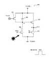
本実施形態では図に示す各発光画素30内にフォトセンサ100を接続する。フォトセンサ100は、一方の端子が第1電源線に接続して電源PVに接続し、他方の端子が駆動TFT6の制御端子(ゲート電極)に接続する。そしてフォトセンサ100の制御端子(ゲート電極)には逆バイアスとなる定電圧Vbiasが印加される。 In this embodiment, the
図4はフォトセンサ100の構造を説明する図である。図4(A)は図3の丸印付近の平面図であり、図3の回路図の端子A、B、C、Dと対応する端子A、B、C、Dを記載した。また、図4(B)は図4(A)のX−X線断面図である。 FIG. 4 is a diagram for explaining the structure of the
フォトセンサは図2のごとく、発光画素30の駆動用TFT6とほぼ同様であるので重複する部分は説明を省略する。 As shown in FIG. 2, the photo sensor is substantially the same as the driving
すなわちフォトセンサ100は、絶縁性基板10上にゲート電極101と、絶縁膜12と、p−S膜よりなる半導体層103とを積層し、半導体層103にチャネル103c、ソース103s、ドレイン103dを設けたTFTである。 That is, in the
このような構造のp−SiTFTでは、TFTがオフ時に半導体層103に外部から光が入射すると、チャネル103cとソース103sまたはチャネル103cとドレイン1103dの接合領域において電子−正孔対が発生する。この電子−正孔対が接合領域の電場のために引き分けられて光起電力が生じてフォトカレントが得られ、フォトカレントは例えばソース電極108側から出力される。すなわち、このフォトカレントはTFTのオフ時の暗電流であり、その増加を検知して、フォトセンサとして利用するものである。 In the p-Si TFT having such a structure, when light is incident on the
ここで、半導体層103には、低濃度不純物領域を設けると良い。低濃度不純物領域とは、ソース103sまたはドレイン103dのチャネル103c側に隣接して設けられ、ソース103sまたはドレイン103dより不純物濃度の低い領域をいう。これを設けることにより、ソース103s(またはドレイン103d)端部に集中する電界を緩和することができる。低濃度不純物領域の領域幅は、例えば0.5μm〜3μm程度である。 Here, a low concentration impurity region is preferably provided in the
本実施形態では例えばチャネルとソース間(またはチャネルとドレイン間)に、低濃度不純物領域103LDを設けて、いわゆるLDD(Light Doped Drain)構造とする。LDD構造にすると、フォトカレントの発生に寄与する接合領域をゲート長L方向に増加させることができるので、フォトカレントが発生しやすくなる。すなわち、少なくともフォトカレントの取出し側に、低濃度不純物領域103LDを設ければよい。また、LDD構造にすることによりVg−Id特性のOFF特性(検出する領域)が安定し、安定したデバイスとなる。 In this embodiment, for example, a low concentration impurity region 103LD is provided between the channel and the source (or between the channel and the drain) to form a so-called LDD (Light Doped Drain) structure. With the LDD structure, the junction region contributing to the generation of the photocurrent can be increased in the gate length L direction, so that the photocurrent is easily generated. That is, the low concentration impurity region 103LD may be provided at least on the photocurrent extraction side. Further, by using the LDD structure, the OFF characteristic (detection region) of the Vg-Id characteristic is stabilized, and a stable device is obtained.
本実施形態のフォトセンサ100は、有機EL素子7の発する光を検知する。従って、有機EL素子7の有機EL層76および陰極75がフォトセンサ100上に延在している。この構造により有機EL素子7の発光がフォトセンサ100の半導体層103に入射し、発光量に応じたフォトカレントがソース領域103s側から出力される。 The
再び図3を参照してこの回路動作を説明する。尚括弧内の電圧値は一例である。 The circuit operation will be described with reference to FIG. 3 again. The voltage values in parentheses are examples.
駆動TFT6と有機EL素子7は電源PV(6V)と電源CV(−6V)間に直列に接続され、フォトセンサ100はnチャネル型TFTであり、データ信号Vdataの最低電圧(0V)より低い逆バイアス(−2V)が印加されている。 The driving
ドレイン線2には電源PV(6V)より低い電圧のデータ信号Vdata(0V〜5V)が入力される。例えば3Vのデータ信号Vdataが入力されると、接続点n1の電圧は3Vとなる。フォトセンサ100がオフ状態で有機EL素子7が発光すると、その光がフォトセンサ100に入射され、有機EL素子7の発光量に応じたフォトカレントが発生する。前述の如くフォトカレントはオフ時の暗電流(リーク電流)であり、すなわち接続点n1の電位は有機EL素子の発光量に応じて電源PVの電位に引かれて上昇する。接続点n1の電位は駆動TFT6のゲート電極に印加されている。従って、有機EL素子7の発光量に応じて接続点n1の電位が上昇すると、駆動TFT6のゲート−ソース間電圧Vgsが小さくなる。これにより有機EL素子7に供給される電流が低減し、当該発光画素30の輝度が小さくなる。 A data signal Vdata (0 V to 5 V) having a voltage lower than that of the power source PV (6 V) is input to the
このように、第1の実施形態では駆動TFT6のVgsが有機EL素子7の発光量に応じて変化する。また、発光量が大きいとフォトセンサ100でのリーク電流量が増加し、駆動TFT6のVgsが小さくなり、有機EL素子7の発光量を小さくする。 Thus, in the first embodiment, Vgs of the driving
つまり同じデータ信号Vdataを与えて輝度の大きさに応じて有機EL素子7の発光量を小さくし、全体として輝度の小さい画素に近づけることができる。従って、消費電力を低減する方向で輝度ムラを補正できる。 That is, the same data signal Vdata can be applied to reduce the light emission amount of the organic EL element 7 in accordance with the luminance level, and the pixel can be brought close to a pixel having a low luminance as a whole. Therefore, luminance unevenness can be corrected in the direction of reducing power consumption.
更に、画素内にフォトセンサ100となるTFTを1つ配置するだけでよく、このTFTは前述の如く画素を構成する駆動TFT6、選択TFT4と同一のプロセスで製造できる。従って画素内の占有面積も小さく、製造工程を複雑にすることなく各画素の輝度ムラを調整することができる。 Further, it is only necessary to dispose one TFT to be the photosensor 100 in the pixel, and this TFT can be manufactured by the same process as the driving
尚、本実施形態のフォトセンサ100は、外光を検知するものではなく有機EL素子の発光量を検知するものである。従って、有機EL層76の光を直接的に半導体層103に入射できるように半導体層103下方にゲート電極101を配置したボトムゲート構造が望ましい(図4参照)。 Note that the
次に、図5から図14を参照して、本発明の第2の実施形態について説明する。第2の実施形態は、画素毎に検知感度が調整可能な受光回路によるフォトセンサ200を設ける場合である。 Next, a second embodiment of the present invention will be described with reference to FIGS. The second embodiment is a case in which a
図5は、有機EL表示装置20を示す概略図である。尚表示部21は第1の実施形態と同様であるので説明は省略する。 FIG. 5 is a schematic view showing the organic
駆動用集積回路50は、輝度調節を行う輝度調節コントローラ51と表示部21にデータ信号Vdataを出力する表示データ補正回路53を有する。また、DC/DCコンバータ56を有しており、有機EL素子に接続する駆動TFTに対して駆動電圧を印加して有機EL素子を発光させる。 The driving
輝度調節コントローラ51は、全ての発光画素30について、フォトセンサ(ここでは不図示)の出力を基に輝度のばらつきを平均化する調整を行う。フォトセンサは外光に対してアナログ出力およびデジタル出力を有しているため、フォトセンサの特性を予め測定することにより外光に対するフォトカレントの関係を得ることができる。 The
具体的には後述するが、参照電圧取得部52において、輝度を平均化するための基準となる輝度(以下基準輝度Lと称する)を取得し、各画素を基準輝度にするための補正値を取得する。補正値は表示データ補正回路53にてデータ信号Vdataに反映される。 Specifically, as will be described later, the reference
表示データ補正回路53は、第1参照電圧と第2参照電圧との間を分圧することにより複数の階調表示電圧を取得する階調基準電圧発生回路54とガンマ補正回路55を備える。ガンマ補正とは、出力輝度が入力信号のガンマ乗に比例する関係を、出力輝度が入力信号に比例する関係に補正することをいう。 The display
そして低電位である第1参照電圧はEL素子の最大輝度レベル(白)であり、高電位である第2参照電圧はEL素子の最小輝度レベル(黒)である。以下、本明細書において、第1参照電圧を白リファレンス電圧、第2参照電圧を黒リファレンス電圧と称する。 The first reference voltage having a low potential is the maximum luminance level (white) of the EL element, and the second reference voltage having a high potential is the minimum luminance level (black) of the EL element. Hereinafter, in the present specification, the first reference voltage is referred to as a white reference voltage, and the second reference voltage is referred to as a black reference voltage.
補正値は、表示データ補正回路53に入力され、階調基準電圧発生回路54の白リファレンス電圧に反映される。階調基準電圧発生回路54は、白リファレンス電圧と黒リファレンス電圧間をRGB各色毎に分圧し、複数の階調表示電圧を発生させる。表示データ補正回路53はデータ信号のD/A(デジタル−アナログ)変換を行い、複数の階調表示電圧によりアナログのRGBのデータ信号が生成され、これを更にガンマ補正回路55にて補正する。そしてこれをデータ信号Vdataとして表示部21に出力し、画像を表示する。これにより表示部21は階調表示電圧に基づいて階調表示される。 The correction value is input to the display
つまり、本実施形態では各発光画素の輝度を基準輝度Lにするための補正値を取得し、それを階調基準電圧発生回路54の白リファレンス電圧に反映するものである。 That is, in the present embodiment, a correction value for setting the luminance of each light emitting pixel to the reference luminance L is acquired and reflected in the white reference voltage of the gradation reference
図6に第2の実施形態の1画素を示す。図6(A)が回路図であり、図6(B)が図6(A)の丸印部分の平面図であり、図6(A)の回路図に対応する端子A、B、C、Dを図6(B)に記載した。図6(B)のY−Y線断面図は、図4(B)と同様であり、説明は省略する。 FIG. 6 shows one pixel of the second embodiment. 6A is a circuit diagram, FIG. 6B is a plan view of a circled portion of FIG. 6A, and terminals A, B, C, and C corresponding to the circuit diagram of FIG. D is shown in FIG. 6 (B). A cross-sectional view taken along line YY in FIG. 6B is the same as FIG. 4B, and description thereof is omitted.
発光画素30は、発光回路180にフォトセンサとなる受光回路200を接続した構成である。基板上には、行方向に延びる複数のゲート線1が配置され、これに交差するように列方向に複数のドレイン線2及び第1電源線3が配置される。第1電源線3は、電源PVに接続されている。電源PVは例えば正の定電圧を出力する電源である。 The
発光回路180は、ゲート線1とドレイン線2とのそれぞれの交点に接続した選択TFT4と、保持コンデンサ5と、駆動TFT6と有機EL素子7とから構成される。選択TFT4のゲートはゲート線1に接続され、選択TFT4のドレインがドレイン線2に接続されている。選択TFT4のソースは保持コンデンサ5と駆動TFT6のゲートに接続されている。 The
駆動TFT6のドレインは、第1電源線3に接続され、ソースは有機EL素子7の陽極に接続されている。有機EL素子7の陰極は電源CVに接続されている。電源CVは負の定電圧を出力する電源である。保持コンデンサ5の対極には、列方向に延在する第2電源線9が接続されている。 The drain of the driving
第1電源線3は、電源PVに接続されている。すなわち、駆動TFT6は、データ信号Vdataの大きさに応じた導電率で第1電源線3と有機EL素子7とを接続する。この結果、データ信号Vdataに応じた電流が駆動TFT6を介して第1電源線3から有機EL素子7に供給され、データ信号Vdataに応じた輝度で有機EL素子7が発光する。 The
保持コンデンサ5は、第2電源線9もしくは第1電源線3など他の電極との間で静電容量を形成しており、一定時間データ信号Vdataを蓄積することができる。 The holding
データ信号Vdataは、Vスキャナが他のゲート線1を選択し、そのゲート線1が非選択となって選択TFT4がオフした後も、保持コンデンサ5によって1垂直走査期間の間保持され、その間、駆動TFT6は前記導電率を保持し、有機EL素子7はその輝度で発光を続けることができる。 The data signal Vdata is held for one vertical scanning period by the holding
駆動TFT6と有機EL素子7とは、正の電源PVと負の電源CVとの間に直列に接続されている。有機EL素子7に流れる駆動電流は、電源PVから駆動TFT6を介して有機EL素子7に供給され、そして、この駆動電流は駆動TFT6のゲート電圧VGを変化させることによって制御することができる。上述したように、ゲート電極にはデータ信号Vdataが入力されており、ゲート電圧VGはデータ信号Vdataに応じた値となる。 The driving
フォトセンサとなる受光回路200は、1つの発光画素30内で、発光回路180のゲート線1、第1電源線3、第2電源線9、センサ出力線8と接続する。センサ出力線8は、受光回路200の抵抗体203の一端と接続し、受光回路(フォトセンサ)200の検出結果を駆動用集積回路50に出力する。尚、第2電源線9は第1電源線3より低電位である。また、図では保持コンデンサ5が第2電源線9に接続しているが、保持コンデンサ5は専用の容量線(不図示)に接続してもよい。 The
図7から図9を参照して第2の実施形態のフォトセンサ200を説明する。 A photosensor 200 according to the second embodiment will be described with reference to FIGS.
図7はフォトセンサ200となる受光回路部分を取り出した回路図である。フォトセンサ200は、フォトトランジスタ205と、容量204と、第1スイッチングトランジスタ201と、第2スイッチングトランジスタ202と、第1接続点n1と、第2接続点n2と、抵抗体203と、第1電源端子T1と第2電源端子T2とを有する。 FIG. 7 is a circuit diagram in which a light receiving circuit portion serving as the
第1電源端子T1は第2電源端子T2より高電位であればよく、ここでは一例として第1電源端子T1をVDD電位、第2電源端子T2をGND電位として説明する。 The first power supply terminal T1 only needs to have a higher potential than the second power supply terminal T2. Here, as an example, the first power supply terminal T1 is described as a VDD potential and the second power supply terminal T2 is described as a GND potential.
第1スイッチングトランジスタ201は入力信号Vpulseが制御端子に入力されることにより導通し、フォトトランジスタ205と直列接続する。そして両者は第1電源端子T1および第2電源端子T2間に接続する。 The
また第2スイッチングトランジスタ202と抵抗体203は直列接続し、これらも第1電源端子T1および第2電源端子T2間に接続する。 The
容量204は一端が第1接続点n1より第2スイッチングトランジスタ202の制御端子に接続し、他端が第1電源端子T1または第2電源端子T2に接続する。容量204は、第1スイッチングトランジスタが導通することにより充電され、第1接続点n1の電位を変動させる。 One end of the
以下、具体的に説明する。容量204は、第1接続点n1によりフォトトランジスタ205の出力端子と一端が接続し、他端が第1電源端子T1に接続する。そして容量204と並列に第1スイッチングトランジスタ201が接続する。第1スイッチングトランジスタ201の制御端子には、所定の期間でパルスが入力される。 This will be specifically described below. The
第2スイッチングトランジスタ202は、第1電源端子T1と第2電源端子T2間に直列に接続され、その制御端子には第1接続点n1からの出力が印加される。一例として第1スイッチングトランジスタ201は、nチャネル型のTFTであり、第2スイッチングトランジスタ202は、pチャネル型のTFTである。これらの構造は、図2の駆動TFT6と同様である。 The
抵抗体203は、第2接続点n2により一端が第2スイッチングトランジスタ202の一端と接続し、他端は第2電源端子T2と接続して接地される。抵抗体203は例えばpチャネル型のTFTであり、その制御端子には定電圧Vaが印加される。TFTのソース−ドレイン間が高抵抗となるように、ゲート電圧Vaを固定するとTFTを抵抗として利用できる。これにより、第2接続点n2からはフォトトランジスタ205で検知したフォトカレントが電圧に変換されて出力され、定電圧Vaの変動により出力される電圧も変動する。尚、この場合ソース−ドレイン間の抵抗値は103Ω〜108Ω程度とする。One end of the
このように第1電源端子T1と第2電源端子T2間に高い抵抗値を有する抵抗体203を接続することにより、フォトトランジスタ205で検知したフォトカレントを電源電位VDDと接地電位GND間の電位差の分圧として出力することができる。第1電源端子T1は、フィードバックとしての利用が容易な範囲に設定すればよい。尚、定電圧Vaの変動や詳細な回路動作については後述する。また、フォトトランジスタ205は、図4(B)と同様な構造であり、説明は省略する。 In this way, by connecting the
尚、本実施形態においては第1および第2スイッチングトランジスタ201、202も、いわゆるLDD構造にすると、ソース(またはドレイン)端部に集中する電界を緩和することができるため好適である。 In the present embodiment, it is preferable that the first and
図7および図8を参照し、フォトセンサ200の動作を説明する。図8(A)はタイミングチャートであり、図8(B)(C)は出力電圧Voutの出力例である。 The operation of the photosensor 200 will be described with reference to FIGS. 8A is a timing chart, and FIGS. 8B and 8C are output examples of the output voltage Vout.
第1スイッチングトランジスタ201の制御端子、すなわちゲート電極に所定電圧Vpulse(Hレベル)のパルスを一定期間入力する。Hレベルのパルスの入力期間、第1スイッチングトランジスタの導通は維持される。これにより容量204には電源電位VDDが充電される。 A pulse of a predetermined voltage Vpulse (H level) is input to the control terminal of the
パルスがLレベル(0V)になると第1スイッチングトランジスタ201が遮断される。本実施形態は第1接続点n1を基準電位(VDD電位)とし、フォトトランジスタ205からの放電によって第1接続点n1の電位を降下させて出力電圧を得る。 When the pulse becomes L level (0 V), the
フォトトランジスタ205に光が照射されると、例えば10−14A〜10−9A程度の非常に微小なフォトカレントが出力される。フォトカレントは前述の如く、フォトトランジスタ205を構成するTFTのオフ時に照射された光量により発生する暗電流である。つまり、光によりフォトトランジスタ205から漏れる電流を検知して光量を検出している。従って、フォトトランジスタ205に光が照射すると、その光量に応じた電荷がフォトトランジスタ205から放電し、図8(A)の実線aで示す如く第1接続点n1の基準電位(VDD電位)が降下していく。When the
第2スイッチングトランジスタ202はpチャネル型TFTであり、その制御端子(ゲート電極)は第1接続点n1に接続している。つまり、第1接続点n1の電位が降下して閾値電圧VTH以下になると、第2スイッチングトランジスタ202が導通する。 The
抵抗体203は、定電圧Vaにより導通しており、定電圧Vaに応じたチャネルが形成されており、抵抗値が一定の抵抗体としてみることができる。出力電圧VOUTは、第1電源端子T1と第2電源端子T2の電位差を、第2スイッチングトランジスタ202の抵抗値と抵抗体203の抵抗分圧で出力することになる。つまり、第2スイッチングトランジスタ202の導通以前は、第2スイッチングトランジスタ202の抵抗値が、抵抗体203の抵抗値より十分大きく、第2接続点n2は第2電源端子T2により近い電圧となる。一方導通すると、第2スイッチングトランジスタ202の抵抗値は、抵抗体203の抵抗値より十分小さくなり、第2接続点n2は第1電源端子T1に近い電圧となる。 The
つまり、フォトトランジスタ205で検知したフォトカレントを、電源電位VDDと接地電位GND間の電位差の分圧として、電源電位VDDに近い出力電圧Voutとして検出することができる。 That is, the photocurrent detected by the
ここで、抵抗体203の抵抗値は非常に高抵抗であるので、微少なフォトカレントであってもフィードバックが容易な程度に十分大きい値の出力電圧Voutを得ることができる。 Here, since the resistance value of the
このようにフォトセンサ200は、第1スイッチングトランジスタ201に電圧Vpulseのパルスを入力するだけで動作可能である。また、回路を構成する構成要素もわずか3つのTFTと1つの容量で実現することができ、部品点数を削減することができる。 As described above, the
図8(B)(C)は、光量による出力電圧Voutの出力例を示す。グラフのX軸は時間を示し、Y軸が出力電圧Voutを示している。実線a、破線a’は同じVa値であるがフォトトランジスタ205で検出した光量が違う場合であり、実線a、bはそれぞれ抵抗体203のVaの違いを示す。 FIGS. 8B and 8C show output examples of the output voltage Vout by the amount of light. The X axis of the graph indicates time, and the Y axis indicates the output voltage Vout. A solid line a and a broken line a 'have the same Va value, but the amount of light detected by the
このグラフより、光量および抵抗体203のVa値と、Voutが出力されている時間との関係が明らかとなる。 From this graph, the relationship between the amount of light and the Va value of the
まず、図8(B)を参照して同じVa値で光量が大きい場合(実線a)と光量が小さい場合(破線a’)について説明する。 First, with reference to FIG. 8B, a case where the amount of light is large with the same Va value (solid line a) and a case where the amount of light is small (broken line a ') will be described.
前述の如く入力信号Vpluseにより基準電位VDDに引き上げられた第1接続点n1の電圧は、フォトトランジスタ205で検知する光量に応じて減少する(図8(A)実線a)。そして第2スイッチングトランジスタ202の閾値電圧を下回り、第2スイッチングトランジスタ202がオンすると、第1電源端子T1から抵抗体(TFT)203に電流が流れる(図8(B):t1)。抵抗体203はゲート電圧Vaに応じたチャネルが形成され所定の時間が経過すると飽和状態となる。これにより一定の抵抗値を有する抵抗体203となり、その時点で電源電圧VDDと抵抗体203の分圧として第2接続点n2より出力電圧Voutが検出できる(図8(B):t2)。 As described above, the voltage at the first connection point n1 raised to the reference potential VDD by the input signal Vpluse decreases according to the amount of light detected by the phototransistor 205 (solid line a in FIG. 8A). When the voltage drops below the threshold voltage of the
さらにある時間が経過した後、第1スイッチングトランジスタ201にVpulseが入力されると第2スイッチングトランジスタ202がオフとなるので、出力電圧Voutはほぼ0Vとなる(t3)。つまり、出力電圧Voutが検出されている時間(Hレベル)、出力電圧Voutが検出されない時間(Lレベル)として二値で検出することができる。 Further, after a certain time has elapsed, when Vpulse is input to the
一方破線a’のごとく光量が少ない場合はフォトトランジスタ205の放電量も少なくなるので、第2スイッチングトランジスタ202の閾値電圧に到達する時間が実線aより遅くなる。すなわち、第2スイッチングトランジスタ202がオンするタイミングが遅くなり(t4)、出力電圧VoutがHレベルとなるタイミングが遅くなる(t5)。一定の周期で第1スイッチングトランジスタ201に入力されるVpluseにより、第2スイッチングトランジスタ202がオフし、出力電圧VoutはLレベルとなる(t3)。抵抗体203が飽和状態となる時間はほぼ一定であるので、第2スイッチングトランジスタ202がオンするタイミングの遅れは、出力電圧VoutがHレベルとなっている期間が短くなることを表わす。 On the other hand, when the amount of light is small as indicated by the broken line a ', the amount of discharge of the
また、Hレベルの期間が長ければそれだけ出力電圧Voutを検出できるタイミングが長いことになるので、フォトセンサとしての感度がよいことになる。従って、フォトセンサ200は、光量の大小(実線a、破線a’)により感度を変えることができる。 In addition, if the H level period is long, the timing at which the output voltage Vout can be detected becomes longer, so the sensitivity as a photosensor is better. Therefore, the sensitivity of the photosensor 200 can be changed depending on the amount of light (solid line a, broken line a ').
次に、図8(C)を参照して同じ光量でVa値が大きい場合(実線a)とVa値が小さい場合(実線b)について説明する。 Next, with reference to FIG. 8C, a case where the Va value is large with the same light amount (solid line a) and a case where the Va value is small (solid line b) will be described.
前述の如く入力信号Vpluse入力により基準電位VDDに引き上げられた第1接続点n1の電圧は、フォトトランジスタ205で検知する光量に応じて減少する(図8(A)実線a)。そして第2スイッチングトランジスタ202の閾値電圧を下回り第2スイッチングトランジスタ202がオンすると、第1電源端子T1から抵抗体(TFT)203に電流が流れる(図8(C):t11)。抵抗体203は大きいゲート電圧Va1に応じたチャネルが形成され所定の時間が経過すると飽和状態となる。これにより一定の抵抗値を有する抵抗体203となり、その時点で電源電圧VDDと抵抗体203の分圧として第2接続点n2より出力電圧Voutが検出できる(図8(C):t12)。 As described above, the voltage at the first connection point n1 raised to the reference potential VDD by the input signal Vpluse is reduced according to the amount of light detected by the phototransistor 205 (solid line a in FIG. 8A). When the voltage drops below the threshold voltage of the
さらにある時間が経過した後、第1スイッチングトランジスタ201にVpulseが入力されると第2スイッチングトランジスタ202がオフとなるので、出力電圧Voutはほぼ0Vとなる(t13)。つまり、出力電圧Voutが検出されている時間(Hレベル)、出力電圧Voutが検出されない時間(Lレベル)として二値で検出することができる。 Further, after a certain time has elapsed, when Vpulse is input to the
一方実線bのごとくVa値が低い(Va2)場合は、光量が同じで有れば第2スイッチングトランジスタ202の閾値電圧に到達する時間は実線aとほぼ同時となる。従って、第2スイッチングトランジスタ202がオンするタイミングも同時となる(t11)。 On the other hand, when the Va value is low (Va2) as indicated by the solid line b, the time for reaching the threshold voltage of the
第2スイッチングトランジスタ202がオンすると、第1電源端子T1から抵抗体(TFT)203に電流が流れる。抵抗体203は低いゲート電圧Va2に応じたチャネルが形成され所定の時間が経過すると飽和状態となり、以降は抵抗体203の抵抗値に応じた分圧で出力電圧Voutが検出できる(t14)。 When the
さらにある時間が経過した後、第1スイッチングトランジスタ201にVpulseが入力されると第2スイッチングトランジスタ202がオフとなるので、出力電圧Voutはほぼ0Vとなる(図8(C):t13)。 Further, after a certain time has elapsed, when Vpulse is input to the
ここで、ゲート電圧Va2が低ければチャネル幅も狭くなるので、飽和状態になる時間がVa1の場合よりも早くなる。従って、出力電圧Voutが検出できるタイミングが早まり、Hレベルになる期間が長くなる(t12→t14)。 Here, if the gate voltage Va2 is low, the channel width is also narrowed, so the time for saturation becomes faster than in the case of Va1. Therefore, the timing at which the output voltage Vout can be detected is advanced, and the period during which the output voltage Vout is at the H level is lengthened (t12 → t14).
つまり、Va値が低ければフォトセンサ200の感度が向上し、Va値の変動により感度を調節することができる。 That is, if the Va value is low, the sensitivity of the
図9を参照して、更に説明する。図9(A)は、抵抗体203のVaと第2スイッチングトランジスタ202のVd−Id特性の一例を示す。c、dが第2スイッチングトランジスタ202のVd−Id特性であり、Va3、Va4が抵抗体(TFT)203のVd−Id特性である。また図9(B)は、図9(A)と対応させて図8(C)の出力例のX軸およびY軸を入れ替えた模式図である。光量はdはcより多く、ゲート電圧はVa3よりVa4が大きいとする。 Further description will be given with reference to FIG. FIG. 9A shows an example of Va of the
図9(A)(B)のごとくゲート電圧Va3の場合、第2スイッチングトランジスタ202の線形領域において抵抗体203との交点x1があり、光量c、dいずれも出力電圧VoutをHレベルとして検知できる。そして光量dの方が光量cよりも検出期間が長くなる。 In the case of the gate voltage Va3 as shown in FIGS. 9A and 9B, there is an intersection x1 with the
一方図9(C)のごとく、ゲート電圧Vaを大きくしすぎる(Va4)と、が第2スイッチングトランジスタの線形領域における交点x2は光量dのみとなる。光量cは抵抗体203の飽和状態で第2スイッチングトランジスタ202も飽和状態となってしまうので、出力電圧Voutを検出することができないことが判る。また、光量dの検出期間も短くなる。 On the other hand, as shown in FIG. 9C, when the gate voltage Va is excessively increased (Va4), the intersection point x2 in the linear region of the second switching transistor is only the light amount d. It can be understood that the output voltage Vout cannot be detected because the amount of light c is saturated when the
従って、第2スイッチングトランジスタ202の線形領域において抵抗体203のVd−Idカーブが交わるように、Vpulse、Vaを適宜選択する。 Therefore, Vpulse and Va are appropriately selected so that the Vd-Id curves of the
このように、フォトセンサ200は、第2スイッチングトランジスタ202のオン・オフによる二値的な出力を得るが、積算面積を算出するなどして出力電圧Voutのアナログ出力が可能であり、第2の実施形態ではアナログ出力を利用する。 As described above, the
第2の実施形態では上記のフォトセンサ200を、図6(A)のごとく、ゲート線1、第1電源線3、第2電源線9に接続する。このようにすることで、フォトセンサ200の第1電源端子T1は表示部21の電源PVを利用し、第2電源端子T2は第2電源線9の電位を利用できる。前述のごとく第2電源線9は第1電源線3より低電位の電源線である。また、ゲート線1と接続することによりフォトセンサの入力信号Vpulseは表示部21のゲート信号と共通にできる。尚出力電圧Voutはセンサ出力線8に出力される。従って画素毎に受光回路を配置する構成であっても、配線の複雑化を回避できる。 In the second embodiment, the
また、抵抗体となるTFT203のゲート電圧Vaを調整することにより、フォトセンサ200の出力電圧Voutの検出感度を変えることができる。 In addition, the detection sensitivity of the output voltage Vout of the photosensor 200 can be changed by adjusting the gate voltage Va of the
特にフォトカレントはフォトトランジスタ205の暗電流であるため、その値にばらつきが生じる。しかし、抵抗体203のゲート電圧Vaにより出力電圧Voutの検出感度を調節できるので、各発光画素30毎にフォトセンサ200の検出感度を一定にすることができる。従って、検出結果のばらつきが少なくなり、より輝度ムラを低減できる。 In particular, since the photocurrent is a dark current of the
更に上記のフォトセンサ200では、抵抗体203のVa値のみならず、フォトトランジスタ205の接続数、入力信号Vpulseの周期、容量204の大きさによっても検出感度を調整することができる。フォトトランジスタ205の接続数は有機EL素子の光を検知した際の放電量に寄与し、入力信号Vpulseの周期は図8のごとく出力電圧VoutがHレベルである期間に寄与する。更に容量204の大きさは、第2スイッチングトランジスタ202のゲート電極に印加される電位であり、V=Q/Cの関係より容量204から電荷が放電することにより電位が変動する。つまり、容量204が小さい方がより検出感度を高めることができる。 Further, in the
尚、図7の回路構成は一例であり、第1スイッチングトランジスタ201、フォトトランジスタ205の接続位置、第2スイッチングトランジスタ202と抵抗体203の接続位置、容量204の接続位置は変更可能である。すなわち、第1スイッチングトランジスタ201を導通させて第1接続点n1の電位を第1電源端子T1または第2電源端子T2の電位に充電し、第1スイッチングトランジスタ201を遮断し、フォトトランジスタ205からの放電により第1接続点n1の電位を変動させ、その電位により第2スイッチングトランジスタ202を導通または遮断させて第2スイッチングトランジスタ202および抵抗体203の第2接続点n2から出力電圧を検出するものであればよい。 7 is an example, and the connection position of the
図10および図11には図7の光量検出回路の他の構成を示す。まず図10は出力電圧Voutが第1電源電位VDDに近い電位で検出できる回路である。 10 and 11 show another configuration of the light amount detection circuit of FIG. First, FIG. 10 shows a circuit that can detect the output voltage Vout at a potential close to the first power supply potential VDD.
図10(A):第1スイッチングトランジスタ201はフォトトランジスタ205と直列接続し、第1電源端子T1および第2電源端子T2間に接続する。第2スイッチングトランジスタ2と抵抗体203は直列接続し、これらも第1電源端子T1および第2電源端子T2間に接続する。第2スイッチングトランジスタ202はpチャネル型TFTであり、抵抗体203はnチャネル型TFTである。容量204はフォトトランジスタ205と並列接続しており、一端が第1接続点n1より第2スイッチングトランジスタ202の制御端子に接続し、他端が第2電源端子T2に接続する。 FIG. 10A: the
第1スイッチングトランジスタ201の制御端子、すなわちゲート電極に所定電圧Vpulse(Hレベル)のパルスを一定期間入力する。Hレベルのパルスの入力期間、第1スイッチングトランジスタ201の導通は維持される。これにより容量204には電源電位VDDが充電される。 A pulse of a predetermined voltage Vpulse (H level) is input to the control terminal of the
パルスがLレベル(0V)になると第1スイッチングトランジスタ201が遮断される。フォトトランジスタ205に光が照射されると、その光量に応じた電荷がフォトトランジスタ205から放電し、第1接続点n1の基準電位(VDD)が降下していく。 When the pulse becomes L level (0 V), the
第2スイッチングトランジスタ202は、第1接続点n1の電位が降下して閾値電圧VTH以下になると導通する。これにより、第2スイッチングトランジスタ202の抵抗値は、抵抗体203の抵抗値より十分小さくなり、第2接続点n2は第1電源端子T1に近い電圧となる。つまり、第2スイッチングトランジスタ202の導通により、フォトトランジスタ205で検知したフォトカレントを電源電位VDDと接地電位GND間の電位差の分圧として、電源電位VDDに近い電位で出力電圧Voutを出力できる。 The
図10(B):第1スイッチングトランジスタ201はフォトトランジスタ205と直列接続し、第1電源端子T1および第2電源端子T2間に接続する。第2スイッチングトランジスタ202と抵抗体203は直列接続し、これらも第1電源端子T1および第2電源端子T2間に接続する。第2スイッチングトランジスタ202はnチャネル型TFTであり、抵抗体203もnチャネル型TFTである。容量204は第1スイッチングトランジスタ201と並列接続しており、一端が第1接続点より第2スイッチングトランジスタ202の制御端子に接続し、他端が第1電源端子T1に接続する。 FIG. 10B: The
第1スイッチングトランジスタ201の制御端子、すなわちゲート電極に所定電圧Vpulse(Hレベル)のパルスを一定期間入力する。Hレベルのパルスの入力期間、第1スイッチングトランジスタの導通は維持される。これにより容量204には電源電位VDDが充電される。 A pulse of a predetermined voltage Vpulse (H level) is input to the control terminal of the
パルスがLレベル(0V)になると第1スイッチングトランジスタ201が遮断される。フォトトランジスタ205に光が照射されると、その光量に応じた電荷がフォトトランジスタ205から放電し、第1接続点n1の基準電位(VDD)が降下していく。 When the pulse becomes L level (0 V), the
nチャネル型TFTの第2スイッチングトランジスタ202は、第1スイッチングトランジスタ201の導通時から第1接続点n1の電位が降下して閾値電圧VTHに達するまでの間導通している。つまり、第2スイッチングトランジスタ202が導通している間は、第2スイッチングトランジスタ202の抵抗値は、抵抗体203の抵抗値より十分小さくなり、第2接続点n2は第2電源端子T2に近い電圧となる。一方閾値電圧VTHより電圧が下がると第2スイッチングトランジスタ202は遮断され、第2スイッチングトランジスタ202の抵抗値が、抵抗体203の抵抗値より十分大きく、第2接続点n2は第1電源端子T1により近い電圧となる。つまり、第2スイッチングトランジスタ202の遮断により、フォトトランジスタ205で検知したフォトカレントを電源電位VDDと接地電位GND間の電位差の分圧として、電源電位VDDに近い電位で出力電圧Voutを出力できる。 The
図10(C):第1スイッチングトランジスタ201はフォトトランジスタ205と直列接続し、第1電源端子T1および第2電源端子T2間に接続する。第2スイッチングトランジスタ202と抵抗体203は直列接続し、これらも第1電源端子T1および第2電源端子T2間に接続する。第2スイッチングトランジスタ202はnチャネル型TFTであり、抵抗体203もnチャネル型TFTである。容量204はフォトトランジスタ205と並列接続しており、一端が第1接続点n1より第2スイッチングトランジスタ202の制御端子に接続し、他端が第2電源端子T2に接続する。 FIG. 10C: the
第1スイッチングトランジスタ201の制御端子、すなわちゲート電極に所定電圧Vpulse(Hレベル)のパルスを一定期間入力する。Hレベルのパルスの入力期間、第1スイッチングトランジスタ201の導通は維持される。これにより容量204には電源電位VDDが充電される。 A pulse of a predetermined voltage Vpulse (H level) is input to the control terminal of the
パルスがLレベル(0V)になると第1スイッチングトランジスタ201が遮断される。フォトトランジスタ205に光が照射されると、その光量に応じた電荷がフォトトランジスタ205から放電し、第1接続点n1の基準電位(VDD)が降下していく。 When the pulse becomes L level (0 V), the
nチャネル型TFTの第2スイッチングトランジスタ202は、第1スイッチングトランジスタ201の導通時から第1接続点n1の電位が降下して閾値電圧VTHに達するまでの間導通している。つまり、第2スイッチングトランジスタ202が導通している間は、第2接続点n2は第2電源端子T2に近い電圧となる。一方第2スイッチングトランジスタ202が遮断されると、第2接続点n2は第1電源端子T1により近い電圧となる。つまり、第2スイッチングトランジスタ202の遮断により、電源電位VDDに近い電位で出力電圧Voutを検出できる。 The
図11は、図7および図10(A)から図10(C)の第1スイッチングトランジスタ201とフォトトランジスタ205の接続を入れ替えた構造であり、この構成により出力電圧Voutは第2電源端子T2の電位に近い電位で検出できる。 FIG. 11 shows a structure in which the connections of the
図11(A):第1スイッチングトランジスタ201はフォトトランジスタ205と直列接続し、第1電源端子T1および第2電源端子T2間に接続する。第2スイッチングトランジスタ202と抵抗体203は直列接続し、これらも第1電源端子T1および第2電源端子T2間に接続する。第2スイッチングトランジスタ202はpチャネル型TFTであり、抵抗体203はnチャネル型TFTである。容量204はフォトトランジスタ205と並列接続しており、一端が第1接続点n1より第2スイッチングトランジスタ202の制御端子に接続し、他端が第1電源端子T1に接続する。 FIG. 11A: The
第1スイッチングトランジスタ201の制御端子、すなわちゲート電極に所定電圧Vpulse(Hレベル)のパルスを一定期間入力する。Hレベルのパルスの入力期間、第1スイッチングトランジスタ201の導通は維持される。これにより容量204には接地電位GNDが充電される。 A pulse of a predetermined voltage Vpulse (H level) is input to the control terminal of the
パルスがLレベル(0V)になると第1スイッチングトランジスタ201が遮断される。フォトトランジスタ205に光が照射されると、その光量に応じた電荷がフォトトランジスタ205から放電し、第1接続点n1の基準電位(GND)が上昇していく。 When the pulse becomes L level (0 V), the
pチャネル型TFTの第2スイッチングトランジスタ202は、第1スイッチングトランジスタ201の導通時から第1接続点n1の電位が降下して閾値電圧VTHに達するまで導通する。これにより、第2スイッチングトランジスタ202の導通時には第2接続点n2は第1電源端子T1に近い電圧となる。一方、第1接続点n1が閾値電圧を超えると第2スイッチングトランジスタ202が遮断される。これにより、第2接続点n2は第2電源端子T2に近い電圧となる。つまり、第2スイッチングトランジスタ202の遮断により接地電位GNDに近い電位で出力電圧Voutを検出できる。 The
図11(B):第1スイッチングトランジスタ201はフォトトランジスタ205と直列接続し、第1電源端子T1および第2電源端子T2間に接続する。第2スイッチングトランジスタ202と抵抗体203は直列接続し、これらも第1電源端子T1および第2電源端子T2間に接続する。第2スイッチングトランジスタ202はpチャネル型TFTであり、抵抗体203はnチャネル型TFTである。容量204は第1スイッチングトランジスタ201と並列接続しており、一端が第1接続点n1より第2スイッチングトランジスタ202の制御端子に接続し、他端が第2電源端子T2に接続する。 FIG. 11B: The
第1スイッチングトランジスタ201の制御端子、すなわちゲート電極に所定電圧Vpulse(Hレベル)のパルスを一定期間入力する。Hレベルのパルスの入力期間、第1スイッチングトランジスタ201の導通は維持される。これにより容量204には接地電位GNDが充電される。 A pulse of a predetermined voltage Vpulse (H level) is input to the control terminal of the
パルスがLレベル(0V)になると第1スイッチングトランジスタ201が遮断される。フォトトランジスタ205に光が照射されると、その光量に応じた電荷がフォトトランジスタ205から放電し、第1接続点n1の基準電位(GND)が上昇していく。 When the pulse becomes L level (0 V), the
pチャネル型TFTの第2スイッチングトランジスタ202は、第1スイッチングトランジスタ201の導通時より第1接続点n1の電位が上昇して閾値電圧VTHに達するまで導通する。これにより、第2接続点n2は第2スイッチングトランジスタ202の導通時には第1電源端子T1に近い電圧となる。一方第1接続点n1の電位が閾値電圧VTHを超えると、第2スイッチングトランジスタ202が遮断し、第2接続点n2は第2電源端子T2に近い電圧となる。つまり、第2スイッチングトランジスタ202の遮断により接地電位GNDに近い電位で出力電圧Voutを検出できる。 The
図11(C):第1スイッチングトランジスタ201はフォトトランジスタ205と直列接続し、第1電源端子T1および第2電源端子T2間に接続する。第2スイッチングトランジスタ202と抵抗体203は直列接続し、これらも第1電源端子T1および第2電源端子T2間に接続する。第2スイッチングトランジスタ202はnチャネル型TFTであり、抵抗体203もnチャネル型TFTである。容量204はフォトトランジスタ205と並列接続しており、一端が第1接続点より第2スイッチングトランジスタ202の制御端子に接続し、他端が第1電源端子T1に接続する。 FIG. 11C: the
第1スイッチングトランジスタ201の制御端子、すなわちゲート電極に所定電圧Vpulse(Hレベル)のパルスを一定期間入力する。Hレベルのパルスの入力期間、第1スイッチングトランジスタ201の導通は維持される。これにより容量204には接地電位GNDが充電される。 A pulse of a predetermined voltage Vpulse (H level) is input to the control terminal of the
パルスがLレベル(0V)になると第1スイッチングトランジスタ201が遮断される。フォトトランジスタ205に光が照射されると、その光量に応じた電荷がフォトトランジスタ205から放電し、第1接続点n1の基準電位(GND)が上昇していく。 When the pulse becomes L level (0 V), the
nチャネル型TFTの第2スイッチングトランジスタ202は、第1接続点n1の電位が閾値電圧VTHに達するまでは遮断しており、閾値電圧VTHを超えると導通する。第2接続点n2は、第2スイッチングトランジスタ202が遮断の間は第1電源端子T1に近い電圧となり、導通すると第2電源端子T2により近い電圧となる。つまり、出力電圧Voutは、第2スイッチングトランジスタ202の導通により接地電位GNDに近い電位で出力できる。 The
図11(D):第1スイッチングトランジスタ201はフォトトランジスタ205と直列接続し、第1電源端子T1および第2電源端子T2間に接続する。第2スイッチングトランジスタ202と抵抗体203は直列接続し、これらも第1電源端子T1および第2電源端子T2間に接続する。第2スイッチングトランジスタ202はnチャネル型TFTであり、抵抗体203もnチャネル型TFTである。容量204は第1スイッチングトランジスタ201と並列接続しており、一端が第1接続点n1より第2スイッチングトランジスタ202の制御端子に接続し、他端が第2電源端子T2に接続する。 FIG. 11D: The
第1スイッチングトランジスタ201の制御端子、すなわちゲート電極に所定電圧Vpulse(Hレベル)のパルスを一定期間入力する。Hレベルのパルスの入力期間、第1スイッチングトランジスタ201の導通は維持される。これにより容量204には接地電位GNDが充電される。 A pulse of a predetermined voltage Vpulse (H level) is input to the control terminal of the
パルスがLレベル(0V)になると第1スイッチングトランジスタ201が遮断される。フォトトランジスタ205に光が照射されると、その光量に応じた電荷がフォトトランジスタ205から放電し、第1接続点n1の基準電位(GND)が上昇していく。 When the pulse becomes L level (0 V), the
nチャネル型TFTの第2スイッチングトランジスタ202は、第1接続点n1の電位が閾値電圧VTHに達するまでは遮断しており、閾値電圧VTHを超えると導通する。第2接続点n2は、第2スイッチングトランジスタ202が遮断の間は第1電源端子T1に近い電圧となり、導通すると第2電源端子T2により近い電圧となる。つまり、出力電圧Voutは、第2スイッチングトランジスタ202の導通により接地電位GNDに近い電位で出力できる。 The
また、図示は省略するが、抵抗体203として抵抗素子を接続してもよい。抵抗素子は、例えばポリシリコンあるいはITO等にn型不純物をドープするなどして形成され、103Ω〜108Ω程度の高い抵抗値を備えている。この場合、抵抗素子203の抵抗値を変えることで、上記の回路の定電圧Vaを変動したと同じ状況となり、フォトセンサ200の感度を調整することができる。Although illustration is omitted, a resistor element may be connected as the
上記のごとく本実施形態の第2スイッチングトランジスタ202は、図7または図10(A)、図11(A)、図11(B)のごとく高電位の第1電源端子T1に一端が接続する場合にはpチャネル型TFTを使用する。一方、図10(B)、図10(C)、図11(C)、図11(D)のごとく低電位である第2電源端子に第2スイッチングトランジスタ202の一端を接続する場合には、第2スイッチングトランジスタはnチャネル型TFTを使用する。 As described above, the
そして、図6の如く受光回路200として発光回路180に接続する場合には、第1端子T1および第2電源端子T2を、第1電源線3および第2電源線9のいずれかとそれぞれ接続することになる。1つの発光画素30における電位は、PV電源>CV電源の関係が成り立っていればよいので、第1電源線3および第2電源線9の電位関係により図7および図10、11の回路を適宜選択する。 When the
図12は、輝度調節コントローラ51を説明する図であり、図12(A)はブロック図、図12(B)は参照電圧取得部52が保持する特性図の一例である。 12A and 12B are diagrams for explaining the
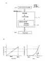
輝度調節コントローラ51にはフォトセンサ200の検出結果(各発光画素の輝度)が入力される。尚、第2の実施形態のフォトセンサ(受光回路)200は、輝度によりオンしているタイミングが異なるものであり、オン状態のパルス部の面積を積分することによりアナログ値を得ることができるものである。 The
すなわち、輝度調節コントローラ51には図の如くパルス波形が入力される。輝度調節コントローラ51内の積分回路はパルス波形を積分して面積を算出しアナログDC波形を得る。 That is, the pulse waveform is input to the
参照電圧取得部52では図12(B)の左図の如き特性図により、フォトセンサ200の出力に応じた発光画素30の輝度を算出し、基準輝度Lとを比較する。例えば画素1では基準輝度Lにするためには輝度を小さくする必要があり、画素2は輝度を大きくする必要がある。また、輝度と参照電圧には図12(B)右図の如き関係があるので、各画素30毎に基準輝度Lに合わせた参照電圧を補正値Vsigとして取得する。補正値Vsigは階調基準電圧発生回路54に出力される。 The reference
基準輝度Lは、例えば全発光画素30の輝度の平均でもよいし、発光輝度の小さい画素に合わせてもよい。また、予め基準輝度Lを設定しておいてもよい。 The reference luminance L may be, for example, the average luminance of all the
又、補正値Vsigは、基準輝度Lに対応した白リファレンス電圧値を取得するようにしてもよいし、画素毎に基準輝度Lに対応した白リファレンス電圧になるような加減値を求めそれを補正値Vsigとして出力してもよい。 As the correction value Vsig, a white reference voltage value corresponding to the reference luminance L may be acquired, or an addition / subtraction value so that a white reference voltage corresponding to the reference luminance L is obtained for each pixel is corrected. You may output as value Vsig.
輝度調節コントローラ51から出力される補正値Vsigは、階調基準電圧発生回路54の白リファレンス電圧に反映され、ガンマ補正回路55にてガンマ補正を行い、ドレイン線2のデータ信号Vdataとして表示部21に送信する(図5参照)。 The correction value Vsig output from the
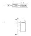
図13は表示データ補正回路53を説明する図である。図13(A)はブロック図、図13(B)は階調基準電圧発生回路54の回路図である。 FIG. 13 is a diagram for explaining the display
表示データ補正回路53に、階調基準電圧発生回路54とガンマ補正回路55を備えており、既述のごとく出力された補正値Vsigが、階調基準電圧発生回路54に入力される。 The display
階調基準電圧発生回路54は階調数(256)に応じた数の抵抗が直列に接続された抵抗分割回路である。そして白リファレンス電圧はEL素子の最高輝度レベル(白)である低電位の参照電圧であり、黒リファレンス電圧はEL素子の最低輝度レベル(黒)である高電位の参照電圧である。 The gradation reference
本実施形態ではこの回路において、黒リファレンス電圧は固定とし、補正値Vsigを階調基準電圧発生回路54の白リファレンス電圧に反映させる。例えば、基準輝度Lに対応した白リファレンス電圧値を補正値Vsigとして出力した場合にはその値を設定する。また、基準輝度Lに対応する白リファレンス電圧に対する加減値を補正値Vsigとして出力した場合には補正値Vsigにより白リファレンス電圧を変動させる。 In this embodiment, in this circuit, the black reference voltage is fixed, and the correction value Vsig is reflected in the white reference voltage of the gradation reference
白リファレンス電圧を変動させる理由を説明する。コントラストCRは、白の輝度と黒の輝度の差であり、製品出荷時には屋内で十分なコントラストCRが得られる(黒が十分に「黒」と視認できる)ように調整されている。 The reason for changing the white reference voltage will be described. The contrast CR is the difference between the brightness of white and the brightness of black, and is adjusted so that a sufficient contrast CR can be obtained indoors (black can be sufficiently recognized as “black”) when the product is shipped.
すなわち黒の輝度は十分小さく、0に近い値となる。従って、輝度を調整するには白の輝度を調整すればよく、白リファレンス電圧の変動により実現できる。 That is, the luminance of black is sufficiently small and is close to 0. Therefore, the brightness can be adjusted by adjusting the brightness of white, which can be realized by changing the white reference voltage.
階調基準電圧発生回路54は、補正された白リファレンス電圧(Vsig)と、黒リファレンス電圧(固定値)間で階調表示電圧を発生させる。 The gradation reference
階調基準電圧発生回路54によって発生した256種類の階調表示用のアナログ電圧(階調表示電圧)は、データ信号としてRGB毎にゲート信号線を介して表示部21内の発光画素30に出力される。 256 kinds of analog voltages for gray scale display (gray scale display voltages) generated by the gray scale reference
以上、各発光画素30の輝度を補正する例を説明したが、これを輝度半減期の調整に利用することもできる。 The example of correcting the luminance of each
図14は、有機EL素子の輝度と時間の関係を示した特性図である。図の如く、有機EL素子は輝度半減期がある。第2の実施形態により全発光画素の輝度が製品出荷時より小さくなっている場合(L→L3)には、図14(B)のごとく補正値Vsigにより劣化した分の白リファレンス電圧を上乗せすることにより、輝度半減期を長くできる。これにより有機EL表示装置の長寿命化に寄与することができる。 FIG. 14 is a characteristic diagram showing a relationship between luminance and time of the organic EL element. As shown in the figure, the organic EL element has a luminance half-life. When the luminance of all the light emitting pixels is lower than that at the time of product shipment according to the second embodiment (L → L3), the white reference voltage that is deteriorated by the correction value Vsig is added as shown in FIG. Thus, the luminance half-life can be increased. This can contribute to extending the life of the organic EL display device.
また、輝度補正と輝度半減期の調整とを併用してもよく、これにより表示品質のよい長寿命の有機EL表示装置を提供できる。 Further, luminance correction and adjustment of luminance half-life may be used in combination, thereby providing a long-life organic EL display device with good display quality.
尚、本実施形態では、画素30が有機EL層76と陽極71、陰極75の積層順を逆にし、紙面上方に発光させるトップエミッション構造であっても同様に実施できるが、その場合であってもフォトセンサ100、200はボトムゲート構造にするとよい。 In the present embodiment, the
1 ゲート線
2 ドレイン線
3 第1電源線
4 選択TFT
5 容量
6 駆動TFT
7 有機EL素子
9 第2電源線
10 絶縁性基板
12 ゲート絶縁膜
14 バッファ層
15 層間絶縁膜
17 平坦化膜
66、106 ドレイン電極
68、108 ソース電極
20 有機EL表示装置
21 表示部
22 Hスキャナ
23 Vスキャナ
30 発光画素
50 駆動用集積回路
51 輝度調節コントローラ
52 参照電圧取得部
53 表示データ補正回路
54 階調基準電圧発生回路
55 ガンマ補正回路
56 DC/DCコンバータ
61、101 ゲート電極
63、103 半導体層
63s、103s ソース
63d、103d ゲート
63c、103c チャネル
71 陽極
72 ホール輸送層
73 発光層
74 電子輸送層
75 陰極
100 フォトセンサ
103LD LDD領域
130 表示画素
201 第1スイッチングトランジスタ
202 第2スイッチングトランジスタ
203 抵抗体
204 容量
205 フォトトランジスタ
1
5
7
DESCRIPTION OF
Claims (10)
Translated fromJapanese前記ドレイン線およびゲート線の交点付近に接続し、駆動トランジスタおよび選択トランジスタおよび有機EL素子からなる発光画素を複数配置した表示部と、
前記発光画素内に設けられたフォトセンサとを具備し、
前記フォトセンサにより前記有機EL素子の発光量を検知し、該有機EL素子の輝度補正を行うことを特徴とする有機EL表示装置。Drain and gate lines arranged in a matrix on the substrate;
A display unit that is connected near the intersection of the drain line and the gate line, and in which a plurality of light emitting pixels including a drive transistor, a selection transistor, and an organic EL element are arranged,
A photosensor provided in the light emitting pixel,
An organic EL display device, wherein the photosensor detects a light emission amount of the organic EL element and performs luminance correction of the organic EL element.
前記ドレイン線およびゲート線の交点付近に接続し、駆動トランジスタおよび選択トランジスタおよび有機EL素子からなる発光画素を複数配置した表示部と、
前記発光画素内に設けられたフォトセンサとを具備し、
前記フォトセンサは、一方の端子が前記駆動トランジスタの電源端子に接続し他方の端子が前記駆動トランジスタの制御端子に接続し制御端子に定電圧が印加されるトランジスタよりなり、前記有機EL素子の発光量を検知して該有機EL素子の輝度補正を行うことを特徴とする有機EL表示装置。Drain and gate lines arranged in a matrix on the substrate;
A display unit that is connected near the intersection of the drain line and the gate line, and in which a plurality of light emitting pixels including a drive transistor, a selection transistor, and an organic EL element are arranged,
A photosensor provided in the light emitting pixel,
The photosensor includes a transistor having one terminal connected to the power supply terminal of the driving transistor and the other terminal connected to the control terminal of the driving transistor, and a constant voltage applied to the control terminal. An organic EL display device which detects the amount and corrects the luminance of the organic EL element.
前記ドレイン線およびゲート線の交点付近に接続し、駆動トランジスタおよび選択トランジスタおよび有機EL素子からなる発光画素を複数配置した表示部と、
前記発光画素内に設けられたフォトセンサとを具備し、
前記フォトセンサは、前記ゲート線および前記ドレイン線および前記駆動トランジスタに接続する複数のトランジスタを少なくとも有し受光感度を調整可能な受光回路で構成され、前記有機EL素子の発光量を検知して該有機EL素子の輝度補正を行うことを特徴とする有機EL表示装置。Drain and gate lines arranged in a matrix on the substrate;
A display unit that is connected near the intersection of the drain line and the gate line, and in which a plurality of light emitting pixels including a drive transistor, a selection transistor, and an organic EL element are arranged,
A photosensor provided in the light emitting pixel,
The photosensor includes a light receiving circuit having at least a plurality of transistors connected to the gate line, the drain line, and the driving transistor and capable of adjusting light receiving sensitivity, and detects a light emission amount of the organic EL element to detect the light emission amount. An organic EL display device which performs luminance correction of an organic EL element.
第1および第2スイッチングトランジスタと、抵抗体と、容量を備え、
前記発光画素に接続する第1電源線および第2電源線間に前記第1スイッチングトランジスタおよびフォトトランジスタを直列接続し、前記第1電源線と前記第2電源線間に前記第2スイッチングトランジスタと前記抵抗体を直列接続し、前記容量の一端は第1接続点より前記第2スイッチングトランジスタの制御端子に接続し、他端は前記第1電源線と接続し、前記抵抗体の抵抗値により前記受光感度を調整することを特徴とする請求項5に記載の有機EL表示装置。The photo sensor includes a gate electrode, an insulating film, and a semiconductor layer stacked on a substrate, a channel provided in the semiconductor layer, a source and a drain provided on both sides of the channel, and received light. A phototransistor that converts it into an electrical signal;
A first and second switching transistor, a resistor, and a capacitor;
The first switching transistor and the phototransistor are connected in series between a first power supply line and a second power supply line connected to the light emitting pixel, and the second switching transistor and the second power supply line are connected between the first power supply line and the second power supply line. A resistor is connected in series, one end of the capacitor is connected from the first connection point to the control terminal of the second switching transistor, the other end is connected to the first power supply line, and the light reception is performed by the resistance value of the resistor. 6. The organic EL display device according to claim 5, wherein the sensitivity is adjusted.
The organic EL display device according to claim 9, wherein the low-concentration impurity region is provided on a side that outputs a photocurrent generated by incident light.
Priority Applications (6)
| Application Number | Priority Date | Filing Date | Title |
|---|---|---|---|
| JP2004205256AJP2006030317A (en) | 2004-07-12 | 2004-07-12 | Organic el display device |
| TW094123335ATW200603660A (en) | 2004-07-12 | 2005-07-11 | Organic electroluminescence (EL) display device |
| US11/178,601US20060012311A1 (en) | 2004-07-12 | 2005-07-12 | Organic electroluminescent display device |
| CNA2005100843234ACN1734541A (en) | 2004-07-12 | 2005-07-12 | Organic electro-luminescent display device |
| EP05015064AEP1617399A2 (en) | 2004-07-12 | 2005-07-12 | Organic electroluminescent display device |
| KR1020050062677AKR20060050070A (en) | 2004-07-12 | 2005-07-12 | Organic EL display |
Applications Claiming Priority (1)
| Application Number | Priority Date | Filing Date | Title |
|---|---|---|---|
| JP2004205256AJP2006030317A (en) | 2004-07-12 | 2004-07-12 | Organic el display device |
Publications (1)
| Publication Number | Publication Date |
|---|---|
| JP2006030317Atrue JP2006030317A (en) | 2006-02-02 |
Family
ID=35169694
Family Applications (1)
| Application Number | Title | Priority Date | Filing Date |
|---|---|---|---|
| JP2004205256AWithdrawnJP2006030317A (en) | 2004-07-12 | 2004-07-12 | Organic el display device |
Country Status (6)
| Country | Link |
|---|---|
| US (1) | US20060012311A1 (en) |
| EP (1) | EP1617399A2 (en) |
| JP (1) | JP2006030317A (en) |
| KR (1) | KR20060050070A (en) |
| CN (1) | CN1734541A (en) |
| TW (1) | TW200603660A (en) |
Cited By (14)
| Publication number | Priority date | Publication date | Assignee | Title |
|---|---|---|---|---|
| JP2008083452A (en)* | 2006-09-28 | 2008-04-10 | Sony Corp | Pixel circuit and display device |
| JP2008091037A (en)* | 2006-09-29 | 2008-04-17 | Seiko Epson Corp | Organic electroluminescence device |
| JP2010266492A (en)* | 2009-05-12 | 2010-11-25 | Sony Corp | Pixel circuit, display apparatus, and driving method for pixel circuit |
| US7888150B2 (en) | 2006-11-15 | 2011-02-15 | Samsung Electronics Co., Ltd. | Display and method of manufacturing the same |
| JP2011141417A (en)* | 2010-01-07 | 2011-07-21 | Sony Corp | Display apparatus, light detection method and electronic apparatus |
| US7994517B2 (en) | 2006-06-09 | 2011-08-09 | Samsung Mobile Display Co., Ltd. | Organic light-emitting display device and method for fabricating the same |
| JP2012208274A (en)* | 2011-03-29 | 2012-10-25 | Sony Corp | Display panel, display device and electronic apparatus |
| JP2012256020A (en)* | 2010-12-15 | 2012-12-27 | Semiconductor Energy Lab Co Ltd | Semiconductor device and driving method for the same |
| KR101419238B1 (en) | 2007-12-31 | 2014-07-15 | 엘지디스플레이 주식회사 | Light emitting display and driving method thereof |
| US8797311B2 (en) | 2009-09-01 | 2014-08-05 | Samsung Display Co., Ltd. | Organic light emitting display and image compensating method thereof |
| KR20140141709A (en)* | 2006-09-29 | 2014-12-10 | 오스람 옵토 세미컨덕터스 게엠베하 | Organic lighting device and lighting equipment |
| CN109742113A (en)* | 2019-01-08 | 2019-05-10 | 京东方科技集团股份有限公司 | An array substrate, its preparation method and related device |
| JP2019525209A (en)* | 2016-07-20 | 2019-09-05 | 京東方科技集團股▲ふん▼有限公司Boe Technology Group Co.,Ltd. | Light emission control circuit, display device including light emission control circuit, and driving method thereof |
| US11475696B2 (en) | 2017-11-23 | 2022-10-18 | Samsung Display Co., Ltd. | Display device and method of operating the display device |
Families Citing this family (124)
| Publication number | Priority date | Publication date | Assignee | Title |
|---|---|---|---|---|
| JP3959454B2 (en)* | 2001-10-22 | 2007-08-15 | シャープ株式会社 | Input device and input / output device |
| CA2443206A1 (en) | 2003-09-23 | 2005-03-23 | Ignis Innovation Inc. | Amoled display backplanes - pixel driver circuits, array architecture, and external compensation |
| JP2006013407A (en)* | 2004-05-21 | 2006-01-12 | Sanyo Electric Co Ltd | Light amount detection circuit and display panel using the same |
| CA2472671A1 (en) | 2004-06-29 | 2005-12-29 | Ignis Innovation Inc. | Voltage-programming scheme for current-driven amoled displays |
| JP2006029832A (en)* | 2004-07-12 | 2006-02-02 | Sanyo Electric Co Ltd | Light intensity detection circuit |
| JP2006079589A (en)* | 2004-08-05 | 2006-03-23 | Sanyo Electric Co Ltd | Touch panel |
| CA2490858A1 (en) | 2004-12-07 | 2006-06-07 | Ignis Innovation Inc. | Driving method for compensated voltage-programming of amoled displays |
| US9171500B2 (en) | 2011-05-20 | 2015-10-27 | Ignis Innovation Inc. | System and methods for extraction of parasitic parameters in AMOLED displays |
| US20140111567A1 (en) | 2005-04-12 | 2014-04-24 | Ignis Innovation Inc. | System and method for compensation of non-uniformities in light emitting device displays |
| US9280933B2 (en) | 2004-12-15 | 2016-03-08 | Ignis Innovation Inc. | System and methods for extraction of threshold and mobility parameters in AMOLED displays |
| TWI402790B (en) | 2004-12-15 | 2013-07-21 | Ignis Innovation Inc | Method and system for programming, calibrating and driving a light-emitting element display |
| US10012678B2 (en) | 2004-12-15 | 2018-07-03 | Ignis Innovation Inc. | Method and system for programming, calibrating and/or compensating, and driving an LED display |
| US9799246B2 (en) | 2011-05-20 | 2017-10-24 | Ignis Innovation Inc. | System and methods for extraction of threshold and mobility parameters in AMOLED displays |
| US8576217B2 (en) | 2011-05-20 | 2013-11-05 | Ignis Innovation Inc. | System and methods for extraction of threshold and mobility parameters in AMOLED displays |
| US10013907B2 (en) | 2004-12-15 | 2018-07-03 | Ignis Innovation Inc. | Method and system for programming, calibrating and/or compensating, and driving an LED display |
| US9275579B2 (en) | 2004-12-15 | 2016-03-01 | Ignis Innovation Inc. | System and methods for extraction of threshold and mobility parameters in AMOLED displays |
| CA2496642A1 (en) | 2005-02-10 | 2006-08-10 | Ignis Innovation Inc. | Fast settling time driving method for organic light-emitting diode (oled) displays based on current programming |
| US20070008297A1 (en)* | 2005-04-20 | 2007-01-11 | Bassetti Chester F | Method and apparatus for image based power control of drive circuitry of a display pixel |
| JP5355080B2 (en) | 2005-06-08 | 2013-11-27 | イグニス・イノベイション・インコーポレーテッド | Method and system for driving a light emitting device display |
| KR100667079B1 (en)* | 2005-08-31 | 2007-01-10 | 삼성에스디아이 주식회사 | Auto Brightness Organic Electroluminescent Display |
| CA2518276A1 (en) | 2005-09-13 | 2007-03-13 | Ignis Innovation Inc. | Compensation technique for luminance degradation in electro-luminance devices |
| KR101169095B1 (en)* | 2005-12-26 | 2012-07-26 | 엘지디스플레이 주식회사 | organic electroluminescence display device and method for fabricating the same |
| US9269322B2 (en) | 2006-01-09 | 2016-02-23 | Ignis Innovation Inc. | Method and system for driving an active matrix display circuit |
| WO2007079572A1 (en) | 2006-01-09 | 2007-07-19 | Ignis Innovation Inc. | Method and system for driving an active matrix display circuit |
| US9489891B2 (en) | 2006-01-09 | 2016-11-08 | Ignis Innovation Inc. | Method and system for driving an active matrix display circuit |
| US20070164293A1 (en)* | 2006-01-13 | 2007-07-19 | Matsushita Electric Industrial Co., Ltd. | Light-emitting device and method for the production of light-emitting device |
| KR101367139B1 (en) | 2006-02-06 | 2014-02-26 | 삼성디스플레이 주식회사 | Display device and manufacturing method of the same |
| EP1816681A3 (en)* | 2006-02-06 | 2012-05-30 | Samsung Electronics Co., Ltd. | Display device and manufacturing method of the same |
| TW200746022A (en) | 2006-04-19 | 2007-12-16 | Ignis Innovation Inc | Stable driving scheme for active matrix displays |
| KR100769444B1 (en)* | 2006-06-09 | 2007-10-22 | 삼성에스디아이 주식회사 | Organic electroluminescent display |
| CA2556961A1 (en) | 2006-08-15 | 2008-02-15 | Ignis Innovation Inc. | Oled compensation technique based on oled capacitance |
| US20080061678A1 (en)* | 2006-09-12 | 2008-03-13 | Matsushita Electric Industrial Co., Ltd. | Light emitting device |
| CN101192362B (en)* | 2006-12-01 | 2010-09-22 | 康佳集团股份有限公司 | On-site single-point adjustment device and adjustment method for LED display screen |
| WO2008081376A2 (en)* | 2007-01-03 | 2008-07-10 | Philips Intellectual Property & Standards Gmbh | Lighting device with a plurality of oled units |
| KR100902233B1 (en) | 2007-03-08 | 2009-06-11 | 삼성모바일디스플레이주식회사 | Organic light emitting display device and manufacturing method |
| KR100882693B1 (en)* | 2007-09-14 | 2009-02-06 | 삼성모바일디스플레이주식회사 | Light emitting display device and manufacturing method thereof |
| US8358258B1 (en)* | 2008-03-16 | 2013-01-22 | Nongqiang Fan | Active matrix display having pixel element with light-emitting element |
| EP2277163B1 (en) | 2008-04-18 | 2018-11-21 | Ignis Innovation Inc. | System and driving method for light emitting device display |
| CA2637343A1 (en) | 2008-07-29 | 2010-01-29 | Ignis Innovation Inc. | Improving the display source driver |
| JP4780159B2 (en)* | 2008-08-27 | 2011-09-28 | ソニー株式会社 | Display device and driving method thereof |
| US9370075B2 (en) | 2008-12-09 | 2016-06-14 | Ignis Innovation Inc. | System and method for fast compensation programming of pixels in a display |
| JP2010139782A (en)* | 2008-12-11 | 2010-06-24 | Sony Corp | Display device, method for driving the display device, and program |
| JP5509589B2 (en)* | 2008-12-17 | 2014-06-04 | ソニー株式会社 | Display device and electronic device |
| KR101002659B1 (en)* | 2008-12-23 | 2010-12-20 | 삼성모바일디스플레이주식회사 | Organic light emitting display |
| US10319307B2 (en) | 2009-06-16 | 2019-06-11 | Ignis Innovation Inc. | Display system with compensation techniques and/or shared level resources |
| CA2669367A1 (en) | 2009-06-16 | 2010-12-16 | Ignis Innovation Inc | Compensation technique for color shift in displays |
| US9384698B2 (en) | 2009-11-30 | 2016-07-05 | Ignis Innovation Inc. | System and methods for aging compensation in AMOLED displays |
| CA2688870A1 (en) | 2009-11-30 | 2011-05-30 | Ignis Innovation Inc. | Methode and techniques for improving display uniformity |
| US9311859B2 (en) | 2009-11-30 | 2016-04-12 | Ignis Innovation Inc. | Resetting cycle for aging compensation in AMOLED displays |
| JP5149993B2 (en)* | 2009-06-26 | 2013-02-20 | シャープ株式会社 | Phototransistor and display device including the same |
| JP5312294B2 (en)* | 2009-10-30 | 2013-10-09 | キヤノン株式会社 | Light emitting apparatus and exposure apparatus |
| US8497828B2 (en) | 2009-11-12 | 2013-07-30 | Ignis Innovation Inc. | Sharing switch TFTS in pixel circuits |
| US10996258B2 (en) | 2009-11-30 | 2021-05-04 | Ignis Innovation Inc. | Defect detection and correction of pixel circuits for AMOLED displays |
| US8803417B2 (en) | 2009-12-01 | 2014-08-12 | Ignis Innovation Inc. | High resolution pixel architecture |
| CA2687631A1 (en)* | 2009-12-06 | 2011-06-06 | Ignis Innovation Inc | Low power driving scheme for display applications |
| US10163401B2 (en) | 2010-02-04 | 2018-12-25 | Ignis Innovation Inc. | System and methods for extracting correlation curves for an organic light emitting device |
| US9881532B2 (en) | 2010-02-04 | 2018-01-30 | Ignis Innovation Inc. | System and method for extracting correlation curves for an organic light emitting device |
| US10089921B2 (en) | 2010-02-04 | 2018-10-02 | Ignis Innovation Inc. | System and methods for extracting correlation curves for an organic light emitting device |
| CA2692097A1 (en) | 2010-02-04 | 2011-08-04 | Ignis Innovation Inc. | Extracting correlation curves for light emitting device |
| US20140313111A1 (en) | 2010-02-04 | 2014-10-23 | Ignis Innovation Inc. | System and methods for extracting correlation curves for an organic light emitting device |
| US10176736B2 (en) | 2010-02-04 | 2019-01-08 | Ignis Innovation Inc. | System and methods for extracting correlation curves for an organic light emitting device |
| CA2696778A1 (en)* | 2010-03-17 | 2011-09-17 | Ignis Innovation Inc. | Lifetime, uniformity, parameter extraction methods |
| KR101754949B1 (en)* | 2010-09-06 | 2017-07-07 | 삼성디스플레이 주식회사 | organic luminescence display |
| US8907991B2 (en) | 2010-12-02 | 2014-12-09 | Ignis Innovation Inc. | System and methods for thermal compensation in AMOLED displays |
| US9886899B2 (en) | 2011-05-17 | 2018-02-06 | Ignis Innovation Inc. | Pixel Circuits for AMOLED displays |
| US9606607B2 (en) | 2011-05-17 | 2017-03-28 | Ignis Innovation Inc. | Systems and methods for display systems with dynamic power control |
| US9351368B2 (en) | 2013-03-08 | 2016-05-24 | Ignis Innovation Inc. | Pixel circuits for AMOLED displays |
| US20140368491A1 (en) | 2013-03-08 | 2014-12-18 | Ignis Innovation Inc. | Pixel circuits for amoled displays |
| CN109272933A (en) | 2011-05-17 | 2019-01-25 | 伊格尼斯创新公司 | The method for operating display |
| US9530349B2 (en) | 2011-05-20 | 2016-12-27 | Ignis Innovations Inc. | Charged-based compensation and parameter extraction in AMOLED displays |
| US9466240B2 (en) | 2011-05-26 | 2016-10-11 | Ignis Innovation Inc. | Adaptive feedback system for compensating for aging pixel areas with enhanced estimation speed |
| US9773439B2 (en) | 2011-05-27 | 2017-09-26 | Ignis Innovation Inc. | Systems and methods for aging compensation in AMOLED displays |
| US9881587B2 (en) | 2011-05-28 | 2018-01-30 | Ignis Innovation Inc. | Systems and methods for operating pixels in a display to mitigate image flicker |
| KR20130005098A (en)* | 2011-07-05 | 2013-01-15 | 삼성전자주식회사 | Display apparatus and driving method thereof |
| US10089924B2 (en) | 2011-11-29 | 2018-10-02 | Ignis Innovation Inc. | Structural and low-frequency non-uniformity compensation |
| US9324268B2 (en) | 2013-03-15 | 2016-04-26 | Ignis Innovation Inc. | Amoled displays with multiple readout circuits |
| US8937632B2 (en) | 2012-02-03 | 2015-01-20 | Ignis Innovation Inc. | Driving system for active-matrix displays |
| US9747834B2 (en) | 2012-05-11 | 2017-08-29 | Ignis Innovation Inc. | Pixel circuits including feedback capacitors and reset capacitors, and display systems therefore |
| US8922544B2 (en) | 2012-05-23 | 2014-12-30 | Ignis Innovation Inc. | Display systems with compensation for line propagation delay |
| KR20140054758A (en)* | 2012-10-29 | 2014-05-09 | 삼성디스플레이 주식회사 | Organic light emitting display device and driving method thereof |
| US9786223B2 (en) | 2012-12-11 | 2017-10-10 | Ignis Innovation Inc. | Pixel circuits for AMOLED displays |
| US9336717B2 (en) | 2012-12-11 | 2016-05-10 | Ignis Innovation Inc. | Pixel circuits for AMOLED displays |
| US9830857B2 (en) | 2013-01-14 | 2017-11-28 | Ignis Innovation Inc. | Cleaning common unwanted signals from pixel measurements in emissive displays |
| CN108665836B (en) | 2013-01-14 | 2021-09-03 | 伊格尼斯创新公司 | Method and system for compensating for deviations of a measured device current from a reference current |
| TW201430711A (en)* | 2013-01-31 | 2014-08-01 | Princeton Technology Corp | Smart card |
| US9721505B2 (en) | 2013-03-08 | 2017-08-01 | Ignis Innovation Inc. | Pixel circuits for AMOLED displays |
| CA2894717A1 (en) | 2015-06-19 | 2016-12-19 | Ignis Innovation Inc. | Optoelectronic device characterization in array with shared sense line |
| EP3043338A1 (en) | 2013-03-14 | 2016-07-13 | Ignis Innovation Inc. | Re-interpolation with edge detection for extracting an aging pattern for amoled displays |
| WO2014174427A1 (en) | 2013-04-22 | 2014-10-30 | Ignis Innovation Inc. | Inspection system for oled display panels |
| KR102015397B1 (en)* | 2013-06-28 | 2019-10-21 | 엘지디스플레이 주식회사 | Organic light emitting display device and method for driving the same |
| CN105474296B (en) | 2013-08-12 | 2017-08-18 | 伊格尼斯创新公司 | A method and device for driving a display using image data |
| US9761170B2 (en) | 2013-12-06 | 2017-09-12 | Ignis Innovation Inc. | Correction for localized phenomena in an image array |
| US9741282B2 (en) | 2013-12-06 | 2017-08-22 | Ignis Innovation Inc. | OLED display system and method |
| US9502653B2 (en) | 2013-12-25 | 2016-11-22 | Ignis Innovation Inc. | Electrode contacts |
| DE102015206281A1 (en) | 2014-04-08 | 2015-10-08 | Ignis Innovation Inc. | Display system with shared level resources for portable devices |
| CA2873476A1 (en) | 2014-12-08 | 2016-06-08 | Ignis Innovation Inc. | Smart-pixel display architecture |
| CA2879462A1 (en) | 2015-01-23 | 2016-07-23 | Ignis Innovation Inc. | Compensation for color variation in emissive devices |
| CA2886862A1 (en) | 2015-04-01 | 2016-10-01 | Ignis Innovation Inc. | Adjusting display brightness for avoiding overheating and/or accelerated aging |
| CA2889870A1 (en) | 2015-05-04 | 2016-11-04 | Ignis Innovation Inc. | Optical feedback system |
| CA2892714A1 (en) | 2015-05-27 | 2016-11-27 | Ignis Innovation Inc | Memory bandwidth reduction in compensation system |
| US10373554B2 (en) | 2015-07-24 | 2019-08-06 | Ignis Innovation Inc. | Pixels and reference circuits and timing techniques |
| US10657895B2 (en) | 2015-07-24 | 2020-05-19 | Ignis Innovation Inc. | Pixels and reference circuits and timing techniques |
| CA2898282A1 (en) | 2015-07-24 | 2017-01-24 | Ignis Innovation Inc. | Hybrid calibration of current sources for current biased voltage progra mmed (cbvp) displays |
| CA2900170A1 (en) | 2015-08-07 | 2017-02-07 | Gholamreza Chaji | Calibration of pixel based on improved reference values |
| KR102330860B1 (en)* | 2015-10-05 | 2021-11-25 | 엘지디스플레이 주식회사 | Organic Light Emitting Display Device And Driving Method Of The Same |
| CA2908285A1 (en) | 2015-10-14 | 2017-04-14 | Ignis Innovation Inc. | Driver with multiple color pixel structure |
| KR102636734B1 (en)* | 2016-09-07 | 2024-02-14 | 삼성디스플레이 주식회사 | Organic light emitting diode display |
| KR102709139B1 (en)* | 2016-10-13 | 2024-09-26 | 삼성디스플레이 주식회사 | Display device |
| CN106847154A (en)* | 2017-02-15 | 2017-06-13 | 京东方科技集团股份有限公司 | Method, device and display device for compensating the bad display panel of display |
| US10564774B1 (en) | 2017-04-07 | 2020-02-18 | Apple Inc. | Correction schemes for display panel sensing |
| CN110709994A (en)* | 2017-10-20 | 2020-01-17 | 深圳市柔宇科技有限公司 | Light Sensors and Organic Light Emitting Diode Displays |
| US11380749B2 (en) | 2017-11-03 | 2022-07-05 | Boe Technology Group Co., Ltd. | Display panel, driving method thereof, and display apparatus |
| CN107785406B (en)* | 2017-11-03 | 2020-04-14 | 京东方科技集团股份有限公司 | An organic electroluminescence display panel, a driving method thereof, and a display device |
| TWI674457B (en)* | 2018-05-09 | 2019-10-11 | 友達光電股份有限公司 | Display device and electronic device comprising thereof |
| CN108649059B (en) | 2018-05-14 | 2020-12-08 | 京东方科技集团股份有限公司 | Array substrate, display device and driving method thereof |
| CN110164370B (en)* | 2018-05-14 | 2021-08-10 | 京东方科技集团股份有限公司 | Pixel circuit, compensation assembly, display device and driving method thereof |
| CN110164362B (en) | 2018-06-26 | 2021-08-17 | 京东方科技集团股份有限公司 | Compensation device and method for light-emitting device, display substrate and manufacturing method thereof |
| CN108877614B (en)* | 2018-07-27 | 2021-03-05 | 维沃移动通信有限公司 | LED circuit, display screen, electronic equipment and detection method |
| CN109616054B (en)* | 2019-02-27 | 2020-07-28 | Oppo广东移动通信有限公司 | Brightness compensation method, display and computer storage medium |
| CN109671392B (en)* | 2019-02-27 | 2021-11-19 | Oppo广东移动通信有限公司 | Brightness compensation method, display and computer storage medium |
| TWI714281B (en)* | 2019-09-26 | 2020-12-21 | 友達光電股份有限公司 | Display panel |
| US10796639B1 (en)* | 2019-09-27 | 2020-10-06 | Int Tech Co., Ltd. | Display device and method for calibrating the same |
| CN112614872B (en)* | 2020-11-30 | 2022-07-26 | 厦门天马微电子有限公司 | Organic light emitting display panel and display device thereof |
| CN112712772A (en)* | 2020-12-31 | 2021-04-27 | 深圳市思坦科技有限公司 | LED display adjusting circuit |
Family Cites Families (14)
| Publication number | Priority date | Publication date | Assignee | Title |
|---|---|---|---|---|
| DE69627393T2 (en)* | 1996-11-27 | 2004-02-05 | Hitachi, Ltd. | LIQUID CRYSTAL DISPLAY WITH ACTIVE MATRIX |
| EP1129446A1 (en)* | 1999-09-11 | 2001-09-05 | Koninklijke Philips Electronics N.V. | Active matrix electroluminescent display device |
| GB0014961D0 (en)* | 2000-06-20 | 2000-08-09 | Koninkl Philips Electronics Nv | Light-emitting matrix array display devices with light sensing elements |
| AU2002231535A1 (en)* | 2001-02-16 | 2002-09-04 | Ignis Innovation Inc. | Active pixel sensor for digital imaging |
| JP2002251167A (en) | 2001-02-26 | 2002-09-06 | Sanyo Electric Co Ltd | Display device |
| US6897477B2 (en)* | 2001-06-01 | 2005-05-24 | Semiconductor Energy Laboratory Co., Ltd. | Semiconductor device, manufacturing method thereof, and display device |
| US6777249B2 (en)* | 2001-06-01 | 2004-08-17 | Semiconductor Energy Laboratory Co., Ltd. | Method of repairing a light-emitting device, and method of manufacturing a light-emitting device |
| JP4146421B2 (en)* | 2002-04-26 | 2008-09-10 | 東芝松下ディスプレイテクノロジー株式会社 | EL display device and driving method of EL display device |
| US6975008B2 (en)* | 2003-10-27 | 2005-12-13 | Eastman Kodak Company | Circuit for detecting ambient light on a display |
| KR101032946B1 (en)* | 2004-04-01 | 2011-05-09 | 삼성전자주식회사 | Optical sensor and display device having same |
| JP2006013407A (en)* | 2004-05-21 | 2006-01-12 | Sanyo Electric Co Ltd | Light amount detection circuit and display panel using the same |
| JP2006029832A (en)* | 2004-07-12 | 2006-02-02 | Sanyo Electric Co Ltd | Light intensity detection circuit |
| JP2006079589A (en)* | 2004-08-05 | 2006-03-23 | Sanyo Electric Co Ltd | Touch panel |
| US7462811B2 (en)* | 2004-11-24 | 2008-12-09 | Eastman Kodak Company | Light detection circuit |
- 2004
- 2004-07-12JPJP2004205256Apatent/JP2006030317A/ennot_activeWithdrawn
- 2005
- 2005-07-11TWTW094123335Apatent/TW200603660A/enunknown
- 2005-07-12CNCNA2005100843234Apatent/CN1734541A/enactivePending
- 2005-07-12KRKR1020050062677Apatent/KR20060050070A/ennot_activeAbandoned
- 2005-07-12EPEP05015064Apatent/EP1617399A2/ennot_activeWithdrawn
- 2005-07-12USUS11/178,601patent/US20060012311A1/ennot_activeAbandoned
Cited By (21)
| Publication number | Priority date | Publication date | Assignee | Title |
|---|---|---|---|---|
| US7994517B2 (en) | 2006-06-09 | 2011-08-09 | Samsung Mobile Display Co., Ltd. | Organic light-emitting display device and method for fabricating the same |
| JP2008083452A (en)* | 2006-09-28 | 2008-04-10 | Sony Corp | Pixel circuit and display device |
| KR20140141709A (en)* | 2006-09-29 | 2014-12-10 | 오스람 옵토 세미컨덕터스 게엠베하 | Organic lighting device and lighting equipment |
| US10267507B2 (en) | 2006-09-29 | 2019-04-23 | Osram Oled Gmbh | Organic lighting device and lighting equipment |
| US9829192B2 (en) | 2006-09-29 | 2017-11-28 | Osram Oled Gmbh | Organic lighting device and lighting equipment |
| KR101691274B1 (en)* | 2006-09-29 | 2016-12-29 | 오스람 오엘이디 게엠베하 | Organic lighting device and lighting equipment |
| US9312308B2 (en) | 2006-09-29 | 2016-04-12 | Osram Oled Gmbh | Organic lighting device and lighting equipment |
| JP2008091037A (en)* | 2006-09-29 | 2008-04-17 | Seiko Epson Corp | Organic electroluminescence device |
| US7888150B2 (en) | 2006-11-15 | 2011-02-15 | Samsung Electronics Co., Ltd. | Display and method of manufacturing the same |
| KR101419238B1 (en) | 2007-12-31 | 2014-07-15 | 엘지디스플레이 주식회사 | Light emitting display and driving method thereof |
| JP2010266492A (en)* | 2009-05-12 | 2010-11-25 | Sony Corp | Pixel circuit, display apparatus, and driving method for pixel circuit |
| US8797311B2 (en) | 2009-09-01 | 2014-08-05 | Samsung Display Co., Ltd. | Organic light emitting display and image compensating method thereof |
| JP2011141417A (en)* | 2010-01-07 | 2011-07-21 | Sony Corp | Display apparatus, light detection method and electronic apparatus |
| JP2012256020A (en)* | 2010-12-15 | 2012-12-27 | Semiconductor Energy Lab Co Ltd | Semiconductor device and driving method for the same |
| US9841843B2 (en) | 2010-12-15 | 2017-12-12 | Semiconductor Energy Laboratory Co., Ltd. | Semiconductor device and driving method thereof |
| JP2012208274A (en)* | 2011-03-29 | 2012-10-25 | Sony Corp | Display panel, display device and electronic apparatus |
| JP2019525209A (en)* | 2016-07-20 | 2019-09-05 | 京東方科技集團股▲ふん▼有限公司Boe Technology Group Co.,Ltd. | Light emission control circuit, display device including light emission control circuit, and driving method thereof |
| US11475696B2 (en) | 2017-11-23 | 2022-10-18 | Samsung Display Co., Ltd. | Display device and method of operating the display device |
| CN109742113A (en)* | 2019-01-08 | 2019-05-10 | 京东方科技集团股份有限公司 | An array substrate, its preparation method and related device |
| CN109742113B (en)* | 2019-01-08 | 2020-12-25 | 京东方科技集团股份有限公司 | Array substrate, preparation method thereof and related device |
| US11271049B2 (en) | 2019-01-08 | 2022-03-08 | Boe Technology Group Co., Ltd. | Array substrate, preparation method thereof and related device |
Also Published As
| Publication number | Publication date |
|---|---|
| EP1617399A2 (en) | 2006-01-18 |
| TW200603660A (en) | 2006-01-16 |
| US20060012311A1 (en) | 2006-01-19 |
| KR20060050070A (en) | 2006-05-19 |
| CN1734541A (en) | 2006-02-15 |
Similar Documents
| Publication | Publication Date | Title |
|---|---|---|
| JP2006030317A (en) | Organic el display device | |
| US20060164408A1 (en) | Display device | |
| US10347180B2 (en) | Organic light-emitting pixel driving circuit, driving method thereof, and organic light-emitting display panel | |
| US10909925B2 (en) | Pixel circuit and driving method thereof, display panel and display device | |
| US7554514B2 (en) | Electro-optical device and electronic apparatus | |
| CN101960509B (en) | Display device and control method thereof | |
| US9129554B2 (en) | Organic light-emitting display device with data driver operable with signal line carrying both data signal and sensing signal | |
| US8345069B2 (en) | Display apparatus, driving method for display apparatus and electronic apparatus | |
| US20060016964A1 (en) | Light quantity detection circuit | |
| WO2019218831A1 (en) | Array substrate, and display device and brightness calibration method therefor | |
| US8334822B2 (en) | Display apparatus, driving method for display apparatus and electronic apparatus | |
| US8384829B2 (en) | Display apparatus and display apparatus driving method | |
| US20080252223A1 (en) | Organic EL Display Device | |
| CN109256087B (en) | Display device, pixel driving circuit and driving method thereof | |
| EP1939594A2 (en) | Ambient light sensing circuit and flat panel display including ambient light sensing circuit | |
| JPWO2002075711A1 (en) | Self-luminous display | |
| US11348517B2 (en) | Pixel circuit, driving method thereof and display device | |
| JP2006013407A (en) | Light amount detection circuit and display panel using the same | |
| CN109935205B (en) | Pixel driving circuit and compensation method of pixel driving circuit | |
| KR20040074607A (en) | Active drive type light emitting display device and drive control method thereof | |
| US20100253707A1 (en) | Display device | |
| US20080024476A1 (en) | Display device and driving method thereof | |
| US8665189B2 (en) | Display apparatus and display apparatus driving method | |
| KR101152117B1 (en) | Display device and driving method thereof | |
| US8094253B2 (en) | Display device, driving method of display device, and driving method of display element |
Legal Events
| Date | Code | Title | Description |
|---|---|---|---|
| A621 | Written request for application examination | Free format text:JAPANESE INTERMEDIATE CODE: A621 Effective date:20070711 | |
| A761 | Written withdrawal of application | Free format text:JAPANESE INTERMEDIATE CODE: A761 Effective date:20090423 |