JP2006025852A - Imaging module for endoscope - Google Patents
Imaging module for endoscopeDownload PDFInfo
- Publication number
- JP2006025852A JP2006025852AJP2004204890AJP2004204890AJP2006025852AJP 2006025852 AJP2006025852 AJP 2006025852AJP 2004204890 AJP2004204890 AJP 2004204890AJP 2004204890 AJP2004204890 AJP 2004204890AJP 2006025852 AJP2006025852 AJP 2006025852A
- Authority
- JP
- Japan
- Prior art keywords
- main surface
- substrate
- solid
- imaging device
- integrated circuit
- Prior art date
- Legal status (The legal status is an assumption and is not a legal conclusion. Google has not performed a legal analysis and makes no representation as to the accuracy of the status listed.)
- Withdrawn
Links
Images


Landscapes
- Endoscopes (AREA)
- Solid State Image Pick-Up Elements (AREA)
- Transforming Light Signals Into Electric Signals (AREA)
- Studio Devices (AREA)
- Instruments For Viewing The Inside Of Hollow Bodies (AREA)
Abstract
Translated fromJapaneseDescription
Translated fromJapanese本発明は、電子内視鏡に用いられる内視鏡用撮像モジュールに関し、特に、撮像モジュール内の部品の構成に関する。 The present invention relates to an endoscope imaging module used in an electronic endoscope, and more particularly to the configuration of components in the imaging module.
固体撮像素子として、超小型のCCDやCMOSセンサーが開発され、これらが医療用の電子内視鏡へ応用されている。電子内視鏡は、人体に挿入され、患部等の撮像を行うものであり、小型化が望まれている。 Ultra-small CCD and CMOS sensors have been developed as solid-state imaging devices, and these are applied to medical electronic endoscopes. An electronic endoscope is inserted into a human body and images an affected part or the like, and a reduction in size is desired.
特許文献1に示される固体撮像装置は、CCDに接続されるフレキシブルな回路基板の一方の面側にチップコンデンサやICの電子部品を集中して実装し、他方の面側にケーブルの信号線を接続する出力信号ランド、垂直転送パルスランド、水平転送パルスランド等を集中して配置させている。これにより、固体撮像装置の小型化を図り、かつ高密度パターン配置によるクロストークの影響を防止している。 In the solid-state imaging device disclosed in
また特許文献2に示される電子内視鏡用固体撮像装置は、半導体素子を形成した半導体素子基板上に、薄膜コンデンサが積層された薄膜コンデンサ素子基板と、CCDを形成した固体撮像素子基板と、カラーフィルタとを順に積層し、かつ、固体撮像素子、半導体素子および薄膜コンデンサを電気的に接続する電気的接続材を有する構造を開示している。これにより、小型化、薄型化された内視鏡用固体撮像装置を提供している。 Further, a solid-state imaging device for an electronic endoscope shown in
しかしながら、従来の電子内視鏡用撮像装置には、次のような課題がある。図7は、内視鏡用撮像装置に用いられる撮像モジュールの代表的な構成例を示す断面図である。撮像モジュールは、内視鏡撮像装置の先端部を構成するケースもしくはハウジング内に収容される。撮像モジュールは、CCDやCMOSセンサー等の固体撮像素子10を含み、撮像素子の上面には、その受光面を保護するための矩形状のガラスリッド12が配されている。固体撮像素子10とガラスリッド12の間には、紫外線硬化樹脂などの光学用接着剤14が充填され、両者が固定されている。セラミック基板16は、固体撮像素子10を支持するとともに、固体撮像素子と両面基板26との間の電気的インターフェースを提供する。撮像素子10の上面に形成された突起状のバンプ端子18は、TABテープの外部リード20によってセラミック基板16の側面端子部22に電気的に接続される。また、セラミック基板16の底面の端子部には外部リード24を介してチップコンデンサ28やバッファIC30などがはんだ実装された両面基板26が接続されている。セラミック基板16は、例えば積層セラミック基板を用い、側面端子部22と底面の端子部との間に複数の接続経路を形成している。 However, the conventional imaging apparatus for electronic endoscope has the following problems. FIG. 7 is a cross-sectional view illustrating a typical configuration example of an imaging module used in an endoscope imaging apparatus. The imaging module is housed in a case or a housing that constitutes the distal end portion of the endoscope imaging apparatus. The imaging module includes a solid-
しかし、図8に示すように、撮像素子の仕様などに応じて、撮像素子が必要とするコンデンサ28やバッファIC30が複数個存在する場合には、実装する部品数に合わせてスペースを確保するため、両面基板26を軸方向に長くする必要がある。そうすると、撮像モジュールの全長が長くなってしまい、その結果として、撮像モジュールを収容するケースの外形サイズ、特に長さ方向のサイズが大きくなってしまう。小型化が要求される内視鏡にとって、撮像部分を構成する先端部分が大きくなることは、大きな問題であり、商品価値を左右する大きな原因でもある。 However, as shown in FIG. 8, when there are a plurality of
一方、特許文献1でも、フレキシブル基板上に電子部品を実装するため、同じような課題がある。また、特許文献2に示す撮像装置は、固体撮像素子、薄膜コンデンサ、半導体素子を積層させているが、最下層に半導体素子が配置されており、半導体素子への機械的強度が考慮されておらず、外部からの振動や圧力によって半導体素子にダメージが与えられるおそれがある。 On the other hand,
そこで本発明は、上記従来の課題を解決し、半導体素子を保護しつつ、外形サイズの小型化が可能な内視鏡用撮像モジュールを提供することを目的とする。 SUMMARY OF THE INVENTION Accordingly, an object of the present invention is to solve the above-described conventional problems and provide an imaging module for an endoscope that can reduce the outer size while protecting a semiconductor element.
本発明に係る内視鏡用撮像モジュールは、ガラス部材と、ガラス部材の一方の面側に配された固体撮像素子と、第1の主面とこれに対向する第2の主面を含み、第1の主面が固体撮像素子に近接するように配され、少なくとも固体撮像素子との間で電気的なインターフェースを提供するための第1の接続経路を含む第1の基板と、一方の面に2次元的に設けられた複数の端子を含み、当該複数の端子が第1の基板の第2の主面と対向するように配された半導体集積回路素子と、第1の主面とこれに対向する第2の主面を含み、第1の主面が半導体集積回路素子に近接するように配され、少なくとも半導体集積回路素子との間で電気的なインターフェースを提供するための第2の接続経路を含む第2の基板とを含んで構成される。 An imaging module for an endoscope according to the present invention includes a glass member, a solid-state imaging device arranged on one surface side of the glass member, a first main surface and a second main surface facing the first main surface, A first substrate including a first connection path disposed so that the first main surface is close to the solid-state image sensor and providing an electrical interface with at least the solid-state image sensor, and one surface Includes a plurality of terminals provided two-dimensionally, and the plurality of terminals are arranged so as to face the second main surface of the first substrate, the first main surface, and the first main surface And a second main surface facing the semiconductor integrated circuit element, the first main surface being arranged so as to be close to the semiconductor integrated circuit element, and at least a second main surface for providing an electrical interface with the semiconductor integrated circuit element And a second substrate including a connection path.
好ましくは、第1の基板は、各層に所望の導電パターンが形成された積層セラミック基板を含み、第1の基板は、第1の主面と第2の主面とを接続する側面に導電パターンにより形成された複数の側面端子部と、少なくとも第1または第2の主面に導電パターンにより形成された複数の端子部とを含み、第1の接続経路は、複数の側面端子部と複数の端子部との間に複数の接続経路を含む。同様に、第2の基板は、各層に所望の導電パターンが形成された積層セラミック基板を含み、第2の基板は、第1の主面と第2の主面とを接続する側面に導電パターンにより形成された複数の側面端子部と、少なくとも第1または第2の主面に導電パターンにより形成された複数の端子部とを含み、第2の接続経路は、複数の側面端子部と複数の端子部との間に複数の接続経路を含む。 Preferably, the first substrate includes a multilayer ceramic substrate in which a desired conductive pattern is formed on each layer, and the first substrate has a conductive pattern on a side surface connecting the first main surface and the second main surface. And a plurality of terminal portions formed of conductive patterns on at least the first or second main surface, and the first connection path includes the plurality of side terminal portions and the plurality of side terminal portions. A plurality of connection paths are included between the terminal portions. Similarly, the second substrate includes a multilayer ceramic substrate in which a desired conductive pattern is formed on each layer, and the second substrate has a conductive pattern on a side surface connecting the first main surface and the second main surface. And a plurality of terminal portions formed by conductive patterns on at least the first or second main surface, and the second connection path includes the plurality of side terminal portions and the plurality of side terminal portions. A plurality of connection paths are included between the terminal portions.
好ましくは、固体撮像素子の出力信号は、第1の基板の第1の接続経路を介して半導体集積回路素子の所定の端子に入力される。さらに、第1または第2の基板は内部空間を含み、当該内部空間内に電子部品が配され、電子部品が第1または第2の接続経路に電気的に接続されるようにしてもよい。また、第1の基板と半導体回路集積素子との間に接着剤が充填されるようにしてもよい。 Preferably, the output signal of the solid-state imaging device is input to a predetermined terminal of the semiconductor integrated circuit device via the first connection path of the first substrate. Furthermore, the first or second substrate may include an internal space, an electronic component may be disposed in the internal space, and the electronic component may be electrically connected to the first or second connection path. Further, an adhesive may be filled between the first substrate and the semiconductor circuit integrated element.
本発明の他の内視鏡用撮像モジュールは、ガラス部材と、ガラス部材に対向して配された固体撮像素子と、一方の面に2次元的に設けられた複数の端子を含み、当該一方の面と対向する他方の面を固体撮像素子に接着させた半導体集積回路素子と、第1の主面、第1の主面に対向する第2の主面、および第1の主面と第2の主面とに接続される側面を含み、少なくとも第1の主面または第2の主面と側面との間に複数の電気的な接続経路を有し、第1の主面が半導体集積回路素子の一方の面の複数の端子に接続された基板と、固体撮像素子の端子を基板の側面に電気的に接続する接続リードとを含んで構成される。 Another imaging module for an endoscope of the present invention includes a glass member, a solid-state imaging device disposed to face the glass member, and a plurality of terminals provided two-dimensionally on one surface. A semiconductor integrated circuit device in which the other surface facing the first surface is bonded to the solid-state imaging device, a first main surface, a second main surface facing the first main surface, and the first main surface and the first main surface. 2 having a plurality of electrical connection paths between at least the first main surface or the second main surface and the side surface, the first main surface being a semiconductor integrated circuit. The circuit board includes a substrate connected to a plurality of terminals on one surface of the circuit element, and connection leads that electrically connect the terminals of the solid-state imaging device to the side surface of the substrate.
本発明の他の内視鏡用撮像モジュールは、ガラス部材と、ガラス部材に対向して配された固体撮像素子と、固体撮像素子と積層する方向に配される複数の基板であって、各基板は、第1の主面、第1の主面と対向する第2の主面、および第1の主面と第2の主面とを接続する側面を含み、少なくとも第1の主面または第2の主面と側面との間に電気的な接続経路を含む、前記複数の基板と、複数の基板の各基板間に配される複数の半導体集積回路素子であって、各半導体集積回路素子は、一方の主面に2次元的に配された複数の端子を含み、当該複数の接続端子が近接する基板の第1の主面または第2の主面に接続される、前記複数の半導体集積回路素子と、固体撮像素子の端子と所定の基板の側面および各基板の側面を接続する接続リードとを含んで構成される。 Another imaging module for an endoscope of the present invention includes a glass member, a solid-state imaging device arranged to face the glass member, and a plurality of substrates arranged in a direction in which the solid-state imaging device is stacked. The substrate includes a first main surface, a second main surface facing the first main surface, and a side surface connecting the first main surface and the second main surface, and at least the first main surface or A plurality of semiconductor integrated circuit elements disposed between each of the plurality of substrates and the plurality of substrates, each including an electrical connection path between a second main surface and a side surface; The element includes a plurality of terminals arranged two-dimensionally on one main surface, and the plurality of connection terminals are connected to the first main surface or the second main surface of the substrate adjacent to each other. Semiconductor integrated circuit elements, solid-state image sensor terminals, predetermined substrate side surfaces, and connection leads that connect the side surfaces of each substrate Configured to include a.
本発明に係る内視鏡用撮像モジュールは、半導体集積回路素子を基板でサンドイッチし、かつこれらを固体撮像素子に積層させたので、半導体集積回路素子の機械的な強度を保持しつつ、撮像モジュールの外形サイズ、特に、積層方向のサイズを従来よりも非常に小さくすることができる。これにより撮像モジュールを収容する内視鏡の先端部の外形サイズの小型化を図ることができる。 In the endoscope imaging module according to the present invention, the semiconductor integrated circuit element is sandwiched between the substrates and laminated on the solid-state imaging element, so that the imaging module is maintained while maintaining the mechanical strength of the semiconductor integrated circuit element. The outer size, particularly the size in the stacking direction, can be made much smaller than before. As a result, the outer size of the distal end portion of the endoscope that houses the imaging module can be reduced.
以下、本発明を実施するための最良の形態について図面を参照して説明する。 The best mode for carrying out the present invention will be described below with reference to the drawings.
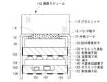
図1は、本発明の第1の実施例に係る内視鏡用撮像モジュールの構成を示す断面図である。なお、従来の説明で用いた図7と同一構成については、同一参照番号を付してある。図1において、本実施例の撮像モジュール100は、ガラスリッド110、CCDまたはCMOSセンサー等の固体撮像素子120、セラミック基板130、半導体集積回路素子140およびセラミック基板150を積層した構造を有する。 FIG. 1 is a cross-sectional view showing a configuration of an endoscope imaging module according to the first embodiment of the present invention. Note that the same reference numerals are assigned to the same components in FIG. 7 used in the conventional description. In FIG. 1, the imaging module 100 of the present embodiment has a structure in which a
ガラスリッド110は、光学用接着剤14を介して固体撮像素子120の受光面側に接着され、固体撮像素子120の裏面は、セラミック基板130によって機械的に支持される。セラミック基板130は、複数のセラミック層を積層した積層基板であり、各層の上面、側面および底面には、所望の複数の導電パターンが形成されている。各セラミック層が積層されたとき、セラミック基板130の側面には、導電パターンによる複数の側面端子部132が形成され、また、底面にも導電パターンによる複数の底面端子部134が形成される。これにより、側面端子部132と底面端子部134との間には、複数の導電経路が形成される。なお、側面端子部132および底面端子部134は、導電パターンの一部であっても良く、あるいは導電パターン上に金属パッド層を含むものであってもよい。 The
セラミック基板130の最上層が接着剤を介して固体撮像素子120に接着される。固体撮像素子120のバンプ端子18は、外部リード20によってセラミック基板130の側面端子部132に電気的に接続される。外部リード20は、側面端子部132とはんだ付け等により接続される。 The uppermost layer of the
好ましくは、固体撮像素子の出力信号が、外部リード20、側面端子部132および底面端子部134を介して半導体集積回路素子140の端子142に入力される。 Preferably, an output signal of the solid-state imaging element is input to the
半導体集積回路素子140は、ウエハーレベルのCSP(チップサイズパッケージ)であり、固体撮像素子110の出力信号を増幅する増幅回路や信号を一時的に保持するバッファ回路などを集積している。半導体集積回路素子140の一方の面には、バンプ状の複数の端子142が設けられ、これらの端子142は、入力端子、出力端子、および電源供給端子等を含んでいる。 The semiconductor
半導体集積回路素子140は、端子142がセラミック基板130の底面端子部134に対向するように位置決めされる。複数の端子142は、底面端子部134とはんだ付けにより接続される。複数の端子142を底面端子部134にはんだ接続することで一定の接合強度は得られるが、より接合強度を増加させるために、セラミック基板130と半導体集積回路素子140との間に接着剤を介在させるようにしてもよい。 The semiconductor
セラミック基板150は、セラミック基板130と同様に、複数のセラミック層を積層した積層基板から構成される。各基板には複数の所望の導電パターンが形成され、各層を積層することで、セラミック基板150の側面および底面に複数の側面端子部152および底面端子部154が形成され、側面端子部152と底面端子部154との間に複数の導電経路が形成される。 Similarly to the
セラミック基板130とセラミック基板150の側面端子部132と152の間は、外部リード156によって接続される。また、セラミック基板150の側面端子部152または底面端子部154には、図示しないケーブルに含まれる外部リード158がはんだ接続される。外部リードは、信号ラインおよび電源供給ライン等を含んでいる。好ましくは、半導体集積回路素子140の出力端子から出力される出力信号は、セラミック基板130の底面端子部134、側面端子部132、外部リード156、セラミック基板150の側面端子部152および底面端子部154を介してケーブルの信号ラインに接続される。また、ケーブルからの電源供給ラインは、セラミック基板150の側面端子部152およびセラミック基板130の側面端子部132を介して直接に固体撮像素子120に供給されるようにしてもよい。この場合、外部リード20と外部リード156とを連結するようにしてもよい。 The
こうして、半導体集積回路素子140は、上下のセラミック基板130、150にサンドイッチされ、外部からの応力や振動に耐えることができる機械的強度を得る。 Thus, the semiconductor integrated
さらに、セラミック基板130、150に挟み込まれた半導体集積回路素子140に種々の電子回路機能を含ませることで、従来の撮像モジュールに必要とされた電子回路部品の一部もしくは全部を省略させることにより、撮像モジュールの長さ方向Lの距離を格段に小さくすることができる。本実施例の撮像モジュールであれば、例えば、ガラスリッド110の厚さを、0.5mm、固体撮像素子120の厚さを0.4mm、セラミック基板130、150の厚さをそれぞれ0、5mm、半導体集積回路素子140の厚さを0.4mmで構成することができ、撮像モジュールの長さLを、約1.8mmとすることができる。従って、撮像モジュールを組み込んだ電子内視鏡の先端部の外形サイズも小型化することが可能となる。 Further, by including various electronic circuit functions in the semiconductor integrated
次に本発明の第2の実施例に係る内視鏡用撮像モジュールの構成を図2に示す。第2の実施例の撮像モジュール101は、半導体集積回路素子140をセラミック基板130を介さずに、固体撮像素子120に接合させている。半導体集積回路素子140およびセラミック基板150は、第1の実施例の状態から180度反転させられている。すなわち、半導体集積回路素子140の他方の面が接着剤等により固体撮像素子120の裏面に接着され、半導体集積回路素子140の一方の面に形成された複数の端子142(入力および出力端子を含む)がセラミック基板150の底面端子部154にそれぞれはんだ付けにより接続されている。 Next, FIG. 2 shows a configuration of an endoscope imaging module according to the second embodiment of the present invention. In the imaging module 101 of the second embodiment, the semiconductor integrated
また、固体撮像素子120のバンプ端子18に接続された外部リード20は、セラミック基板150の側面端子部152に接続されるように延在されている。これにより、固体撮像素子120の出力信号が、側面端子部152、底面端子部154、および入力端子142を介して半導体集積回路素子140に入力される。半導体集積回路素子140の出力信号は、出力端子142、底面端子部154、および側面端子部152を介して信号ラインを構成する外部リード158に接続される。なお、半導体集積回路素子140とセラミック基板150との接合強度を増加させるために、その間に接着剤を充填させても良い。 Further, the
第2の実施例によれば、固体撮像素子の一面を利用して半導体集積回路素子140をセラミック基板150との間で挟持するようにしたので、第1の実施例と比較してセラミック基板を1つ省略することができ、その分だけ、撮像モジュールの長さLを短くすることができる。 According to the second embodiment, since the semiconductor integrated
次に、本発明の第3の実施例に係る内視鏡用撮像モジュールの構成を図3に示す。第3の実施例では、第1の実施例で用いた積層構造において、セラミック基板150内に形成された内部空間160内にコンデンサ等の電子部品162を組み込んだものである。内部空間160内において電子部品162は、所定の導電パターンと電気的に接続される。これにより、半導体集積回路素子とは異なる機能を備えた電子部品を、撮像モジュールの長さLをさほど大きくすることなく実装することができる。 Next, FIG. 3 shows the configuration of an endoscope imaging module according to the third embodiment of the present invention. In the third embodiment, an
次に、本発明の第4の実施例に係る内視鏡用撮像モジュールの構成を図4に示す。第4の実施例では、撮像モジュール104は、第1の実施例の構成に加えて、さらに半導体集積回路素子200、210と、これらの素子をサンドイッチするセラミック基板220、230を備えている。半導体集積回路素子200、210は、第1の実施例と同様に、CSPであり、その一面に複数の端子202、204を備えている。セラミック基板220、230は、第1の実施例と同様に、積層基板であり、複数の側面端子部222、232および複数の底面端子部224、234を含み、それらの端子部間に複数の導電経路を形成する。セラミック基板150、220、230の側面端子部152、222、232は、外部リード240、242によって電気的に接続される。 Next, FIG. 4 shows the configuration of an endoscope imaging module according to the fourth embodiment of the present invention. In the fourth embodiment, the imaging module 104 further includes semiconductor integrated
また、第4の実施例における撮像モジュール104において、第3の実施例に示した電子部品を内部に組み込んだ基板を適用しても良い。図5は、電子部品を内部に組み込んだセラミック基板150の適用例を示している。 Further, in the imaging module 104 in the fourth embodiment, a substrate in which the electronic component shown in the third embodiment is incorporated may be applied. FIG. 5 shows an application example of a
図6は、本実施例による内視鏡用撮像モジュールによる小型化の効果を説明する表である。この表では、半導体集積回路素子の数量を1つから6まで増加させたときの撮像モジュールの長さとその容積を、従来例の場合と対比している。素子数が1とは、撮像モジュールが第1の実施例のように1つの半導体集積回路素子を含む場合である。半導体集積回路素子数が増加したとき、それをサンドイッチするセラミック基板も増加される(例えば、第4の実施例)。設定条件として、セラミック基板の厚さを0.5mm、固体撮像素子の厚さを0.4mm、半導体集積回路素子の厚さを0.4mmとした。本実施例の撮像モジュールの長さLは、ガラスリッドを除いた、固体撮像素子の表面からセラミック基板の底面までの長さLであり(図1を参照)、従来の撮像モジュールは、図7および図8に示すように、固体撮像素子の表面から両面基板の端部までの長さである。また、固体撮像素子や半導体集積回路素子の外形(平面形状)は矩形状であるが、ここでは、直径が3mm(Φ3)の円に近似して計算を行っている。 FIG. 6 is a table for explaining the effect of miniaturization by the endoscope imaging module according to the present embodiment. In this table, the length and the volume of the imaging module when the number of semiconductor integrated circuit elements is increased from 1 to 6 are compared with the case of the conventional example. The number of elements is 1 when the imaging module includes one semiconductor integrated circuit element as in the first embodiment. When the number of semiconductor integrated circuit elements increases, the ceramic substrate sandwiching them increases (for example, the fourth embodiment). As setting conditions, the thickness of the ceramic substrate was 0.5 mm, the thickness of the solid-state imaging device was 0.4 mm, and the thickness of the semiconductor integrated circuit device was 0.4 mm. The length L of the imaging module of this embodiment is the length L from the surface of the solid-state imaging device to the bottom surface of the ceramic substrate excluding the glass lid (see FIG. 1), and the conventional imaging module is shown in FIG. And as shown in FIG. 8, it is the length from the surface of a solid-state image sensor to the edge part of a double-sided board | substrate. In addition, the external shape (planar shape) of the solid-state imaging device or the semiconductor integrated circuit device is rectangular, but here, the calculation is performed by approximating a circle having a diameter of 3 mm (Φ3).
本実施例の場合、集積回路素子数が1つ増加する毎に厚さが0.9mm増加するが、表からも明らかなように、従来方法に比べて撮像モジュールLの長さおよび容積は小さくなり、その結果、容積比も従来の約半分程度に小型化することができる。 In the case of the present embodiment, the thickness increases by 0.9 mm every time the number of integrated circuit elements increases by one, but as is apparent from the table, the length and volume of the imaging module L are smaller than those of the conventional method. As a result, the volume ratio can be reduced to about half of the conventional volume ratio.
以上本発明の好ましい実施の形態について詳述したが、本発明は係る特定の実施形態に限定されるものではなく、特許請求の範囲に記載された本発明の要旨の範囲内において、種々の変形、変更が可能である。 Although the preferred embodiment of the present invention has been described in detail above, the present invention is not limited to the specific embodiment, and various modifications are possible within the scope of the gist of the present invention described in the claims. Can be changed.
本発明に係る内視鏡用撮像モジュールは、医療用の内視鏡用撮像装置や内視鏡撮像システムに利用され、これ以外にも、人間の視覚によって認識することが困難な場所、例えばスペースが限られた配管、あるいは人体に危険があるような機械設備等において利用することができる。 The endoscope imaging module according to the present invention is used in a medical endoscope imaging apparatus or endoscope imaging system, and in addition to this, it is difficult to recognize by human vision, such as a space. However, it can be used in limited piping or in machinery and equipment that is dangerous to the human body.
100、101、102、103、104:内視鏡用撮像モジュール
110:ガラスリッド
120:固体撮像素子
130、150、220、230:セラミック基板
132、152、222、232:側面端子部
134、154、224、234:底面端子部
140、200、210:半導体集積回路素子
142、202、212:端子
20、156、158、240、242:外部リード100, 101, 102, 103, 104: Endoscopic imaging module 110: Glass lid 120: Solid-
Claims (8)
Translated fromJapaneseガラス部材の一方の面側に配された固体撮像素子と、
第1の主面とこれに対向する第2の主面を含み、第1の主面が固体撮像素子に近接するように配され、少なくとも固体撮像素子との間で電気的なインターフェースを提供するための第1の接続経路を含む第1の基板と、
一方の面に2次元的に設けられた複数の端子を含み、当該複数の端子が第1の基板の第2の主面と対向するように配された半導体集積回路素子と、
第1の主面とこれに対向する第2の主面を含み、第1の主面が半導体集積回路素子に近接するように配され、少なくとも半導体集積回路素子との間で電気的なインターフェースを提供するための第2の接続経路を含む第2の基板と、
を含む内視鏡用撮像素子モジュール。A glass member;
A solid-state imaging device disposed on one side of the glass member;
A first main surface and a second main surface opposite to the first main surface, the first main surface being arranged so as to be close to the solid-state image sensor, and providing an electrical interface at least with the solid-state image sensor; A first substrate including a first connection path for
A semiconductor integrated circuit element including a plurality of terminals two-dimensionally provided on one surface, the plurality of terminals being arranged to face the second main surface of the first substrate;
A first main surface and a second main surface opposite to the first main surface, the first main surface being arranged so as to be close to the semiconductor integrated circuit element; and at least an electrical interface with the semiconductor integrated circuit element A second substrate including a second connection path for providing;
An imaging device module for an endoscope including the same.
ガラス部材に対向して配された固体撮像素子と、
一方の面に2次元的に設けられた複数の端子を含み、当該一方の面と対向する他方の面を固体撮像素子に接着させた半導体集積回路素子と、
第1の主面、第1の主面に対向する第2の主面、および第1の主面と第2の主面とに接続される側面を含み、少なくとも第1の主面または第2の主面と側面との間に複数の電気的な接続経路を有し、第1の主面が半導体集積回路素子の一方の面の複数の端子に接続された基板と、
固体撮像素子の端子を基板の側面に電気的に接続する接続リードと、
を含む内視鏡用撮像素子モジュール。A glass member;
A solid-state imaging device arranged facing the glass member;
A semiconductor integrated circuit element including a plurality of terminals provided two-dimensionally on one surface and having the other surface opposed to the one surface bonded to a solid-state imaging device;
Including a first main surface, a second main surface facing the first main surface, and a side surface connected to the first main surface and the second main surface, and at least the first main surface or the second main surface A substrate having a plurality of electrical connection paths between the main surface and the side surface, the first main surface being connected to a plurality of terminals on one surface of the semiconductor integrated circuit element;
A connection lead for electrically connecting the terminal of the solid-state image sensor to the side surface of the substrate;
An imaging device module for an endoscope including the same.
ガラス部材に対向して配された固体撮像素子と、
固体撮像素子と積層する方向に配される複数の基板であって、各基板は、第1の主面、第1の主面と対向する第2の主面、および第1の主面と第2の主面とを接続する側面を含み、少なくとも第1の主面または第2の主面と側面との間に電気的な接続経路を含む、前記複数の基板と、
複数の基板の各基板間に配される複数の半導体集積回路素子であって、各半導体集積回路素子は、一方の主面に2次元的に配された複数の端子を含み、当該複数の接続端子が近接する基板の第1の主面または第2の主面に接続される、前記複数の半導体集積回路素子と、
固体撮像素子の端子と所定の基板の側面および各基板の側面を接続する接続リードと
を含む内視鏡用撮像素子モジュール。A glass member;
A solid-state imaging device arranged facing the glass member;
A plurality of substrates arranged in the direction of stacking with the solid-state imaging device, wherein each substrate includes a first main surface, a second main surface facing the first main surface, and the first main surface and the first main surface. The plurality of substrates, including a side surface connecting the two main surfaces, and including an electrical connection path between at least the first main surface or the second main surface and the side surfaces;
A plurality of semiconductor integrated circuit elements arranged between each of a plurality of substrates, each semiconductor integrated circuit element including a plurality of terminals arranged two-dimensionally on one main surface, wherein the plurality of connections The plurality of semiconductor integrated circuit elements, wherein the terminals are connected to the first main surface or the second main surface of the adjacent substrate;
An imaging device module for an endoscope including a terminal of a solid-state imaging device, a side surface of a predetermined substrate, and a connection lead connecting the side surface of each substrate.
Priority Applications (1)
| Application Number | Priority Date | Filing Date | Title |
|---|---|---|---|
| JP2004204890AJP2006025852A (en) | 2004-07-12 | 2004-07-12 | Imaging module for endoscope |
Applications Claiming Priority (1)
| Application Number | Priority Date | Filing Date | Title |
|---|---|---|---|
| JP2004204890AJP2006025852A (en) | 2004-07-12 | 2004-07-12 | Imaging module for endoscope |
Publications (1)
| Publication Number | Publication Date |
|---|---|
| JP2006025852Atrue JP2006025852A (en) | 2006-02-02 |
Family
ID=35892890
Family Applications (1)
| Application Number | Title | Priority Date | Filing Date |
|---|---|---|---|
| JP2004204890AWithdrawnJP2006025852A (en) | 2004-07-12 | 2004-07-12 | Imaging module for endoscope |
Country Status (1)
| Country | Link |
|---|---|
| JP (1) | JP2006025852A (en) |
Cited By (11)
| Publication number | Priority date | Publication date | Assignee | Title |
|---|---|---|---|---|
| WO2008032404A1 (en)* | 2006-09-15 | 2008-03-20 | Fujitsu Microelectronics Limited | Semiconductor device and method for manufacturing same |
| WO2011030608A1 (en)* | 2009-09-11 | 2011-03-17 | オリンパスメディカルシステムズ株式会社 | Image pickup device and method for manufacturing image pickup device |
| JP2014515955A (en)* | 2011-05-12 | 2014-07-07 | オリーブ・メディカル・コーポレーション | Improved image sensor for endoscope |
| WO2015141802A1 (en)* | 2014-03-20 | 2015-09-24 | オリンパス株式会社 | Method for producing mounting structure, mounting jig, device for producing mounting structure, imaging device, and endoscope device |
| JP2015173736A (en)* | 2014-03-13 | 2015-10-05 | Hoya株式会社 | Semiconductor device and endoscope |
| WO2018021061A1 (en)* | 2016-07-28 | 2018-02-01 | オリンパス株式会社 | Imaging unit and endoscope |
| JP6307697B1 (en)* | 2016-05-10 | 2018-04-11 | オリンパス株式会社 | Electronic circuit unit, imaging unit, imaging module, and endoscope |
| US10075626B2 (en) | 2012-07-26 | 2018-09-11 | DePuy Synthes Products, Inc. | Camera system with minimal area monolithic CMOS image sensor |
| US10750933B2 (en) | 2013-03-15 | 2020-08-25 | DePuy Synthes Products, Inc. | Minimize image sensor I/O and conductor counts in endoscope applications |
| WO2020195872A1 (en)* | 2019-03-27 | 2020-10-01 | Hoya株式会社 | Imaging module and endoscope |
| US10980406B2 (en) | 2013-03-15 | 2021-04-20 | DePuy Synthes Products, Inc. | Image sensor synchronization without input clock and data transmission clock |
- 2004
- 2004-07-12JPJP2004204890Apatent/JP2006025852A/ennot_activeWithdrawn
Cited By (43)
| Publication number | Priority date | Publication date | Assignee | Title |
|---|---|---|---|---|
| WO2008032404A1 (en)* | 2006-09-15 | 2008-03-20 | Fujitsu Microelectronics Limited | Semiconductor device and method for manufacturing same |
| US7939361B2 (en) | 2006-09-15 | 2011-05-10 | Fujitsu Semiconductor Limited | Semiconductor device and method for fabricating semiconductor device |
| KR101100790B1 (en)* | 2006-09-15 | 2012-01-02 | 후지쯔 세미컨덕터 가부시키가이샤 | Semiconductor device and manufacturing method thereof |
| JP5218058B2 (en)* | 2006-09-15 | 2013-06-26 | 富士通セミコンダクター株式会社 | Semiconductor device and manufacturing method thereof |
| WO2011030608A1 (en)* | 2009-09-11 | 2011-03-17 | オリンパスメディカルシステムズ株式会社 | Image pickup device and method for manufacturing image pickup device |
| JP5032704B2 (en)* | 2009-09-11 | 2012-09-26 | オリンパスメディカルシステムズ株式会社 | Imaging apparatus and manufacturing method of imaging apparatus |
| US9763566B2 (en) | 2011-05-12 | 2017-09-19 | DePuy Synthes Products, Inc. | Pixel array area optimization using stacking scheme for hybrid image sensor with minimal vertical interconnects |
| US11432715B2 (en) | 2011-05-12 | 2022-09-06 | DePuy Synthes Products, Inc. | System and method for sub-column parallel digitizers for hybrid stacked image sensor using vertical interconnects |
| US11848337B2 (en) | 2011-05-12 | 2023-12-19 | DePuy Synthes Products, Inc. | Image sensor |
| US9622650B2 (en) | 2011-05-12 | 2017-04-18 | DePuy Synthes Products, Inc. | System and method for sub-column parallel digitizers for hybrid stacked image sensor using vertical interconnects |
| US10709319B2 (en) | 2011-05-12 | 2020-07-14 | DePuy Synthes Products, Inc. | System and method for sub-column parallel digitizers for hybrid stacked image sensor using vertical interconnects |
| US11682682B2 (en) | 2011-05-12 | 2023-06-20 | DePuy Synthes Products, Inc. | Pixel array area optimization using stacking scheme for hybrid image sensor with minimal vertical interconnects |
| US9907459B2 (en) | 2011-05-12 | 2018-03-06 | DePuy Synthes Products, Inc. | Image sensor with tolerance optimizing interconnects |
| US12100716B2 (en) | 2011-05-12 | 2024-09-24 | DePuy Synthes Products, Inc. | Image sensor with tolerance optimizing interconnects |
| US11179029B2 (en) | 2011-05-12 | 2021-11-23 | DePuy Synthes Products, Inc. | Image sensor with tolerance optimizing interconnects |
| US9980633B2 (en) | 2011-05-12 | 2018-05-29 | DePuy Synthes Products, Inc. | Image sensor for endoscopic use |
| US11109750B2 (en) | 2011-05-12 | 2021-09-07 | DePuy Synthes Products, Inc. | Pixel array area optimization using stacking scheme for hybrid image sensor with minimal vertical interconnects |
| JP2014515955A (en)* | 2011-05-12 | 2014-07-07 | オリーブ・メディカル・コーポレーション | Improved image sensor for endoscope |
| US10517471B2 (en) | 2011-05-12 | 2019-12-31 | DePuy Synthes Products, Inc. | Pixel array area optimization using stacking scheme for hybrid image sensor with minimal vertical interconnects |
| US10537234B2 (en) | 2011-05-12 | 2020-01-21 | DePuy Synthes Products, Inc. | Image sensor with tolerance optimizing interconnects |
| US11026565B2 (en) | 2011-05-12 | 2021-06-08 | DePuy Synthes Products, Inc. | Image sensor for endoscopic use |
| US10863894B2 (en) | 2011-05-12 | 2020-12-15 | DePuy Synthes Products, Inc. | System and method for sub-column parallel digitizers for hybrid stacked image sensor using vertical interconnects |
| US11089192B2 (en) | 2012-07-26 | 2021-08-10 | DePuy Synthes Products, Inc. | Camera system with minimal area monolithic CMOS image sensor |
| US10701254B2 (en) | 2012-07-26 | 2020-06-30 | DePuy Synthes Products, Inc. | Camera system with minimal area monolithic CMOS image sensor |
| US11766175B2 (en) | 2012-07-26 | 2023-09-26 | DePuy Synthes Products, Inc. | Camera system with minimal area monolithic CMOS image sensor |
| US10075626B2 (en) | 2012-07-26 | 2018-09-11 | DePuy Synthes Products, Inc. | Camera system with minimal area monolithic CMOS image sensor |
| US11253139B2 (en) | 2013-03-15 | 2022-02-22 | DePuy Synthes Products, Inc. | Minimize image sensor I/O and conductor counts in endoscope applications |
| US10980406B2 (en) | 2013-03-15 | 2021-04-20 | DePuy Synthes Products, Inc. | Image sensor synchronization without input clock and data transmission clock |
| US12150620B2 (en) | 2013-03-15 | 2024-11-26 | DePuy Synthes Products, Inc. | Minimize image sensor I/O and conductor counts in endoscope applications |
| US11903564B2 (en) | 2013-03-15 | 2024-02-20 | DePuy Synthes Products, Inc. | Image sensor synchronization without input clock and data transmission clock |
| US10750933B2 (en) | 2013-03-15 | 2020-08-25 | DePuy Synthes Products, Inc. | Minimize image sensor I/O and conductor counts in endoscope applications |
| US11344189B2 (en) | 2013-03-15 | 2022-05-31 | DePuy Synthes Products, Inc. | Image sensor synchronization without input clock and data transmission clock |
| US10881272B2 (en) | 2013-03-15 | 2021-01-05 | DePuy Synthes Products, Inc. | Minimize image sensor I/O and conductor counts in endoscope applications |
| JP2015173736A (en)* | 2014-03-13 | 2015-10-05 | Hoya株式会社 | Semiconductor device and endoscope |
| US10426324B2 (en) | 2014-03-20 | 2019-10-01 | Olympus Corporation | Imaging apparatus including an image sensor chip mount assembly |
| WO2015141802A1 (en)* | 2014-03-20 | 2015-09-24 | オリンパス株式会社 | Method for producing mounting structure, mounting jig, device for producing mounting structure, imaging device, and endoscope device |
| JP6307697B1 (en)* | 2016-05-10 | 2018-04-11 | オリンパス株式会社 | Electronic circuit unit, imaging unit, imaging module, and endoscope |
| US10610090B2 (en) | 2016-05-10 | 2020-04-07 | Olympus Corporation | Electronic circuit unit, imaging unit, imaging module, and endoscope |
| WO2018021061A1 (en)* | 2016-07-28 | 2018-02-01 | オリンパス株式会社 | Imaging unit and endoscope |
| JP6324644B1 (en)* | 2016-07-28 | 2018-05-16 | オリンパス株式会社 | Imaging unit and endoscope |
| WO2020195872A1 (en)* | 2019-03-27 | 2020-10-01 | Hoya株式会社 | Imaging module and endoscope |
| US11903566B2 (en) | 2019-03-27 | 2024-02-20 | Hoya Corporation | Imaging module and endoscope having image sensor and mounting board |
| JP2020156901A (en)* | 2019-03-27 | 2020-10-01 | Hoya株式会社 | Imaging module and endoscope |
Similar Documents
| Publication | Publication Date | Title |
|---|---|---|
| JP3065378B2 (en) | Circuit board for solid-state imaging device for electronic endoscope | |
| JP3855594B2 (en) | Semiconductor device | |
| JP5926890B2 (en) | Wiring board, manufacturing method of wiring board, and imaging apparatus | |
| CN109952650B (en) | Camera module and endoscope | |
| US11000184B2 (en) | Image pickup module, fabrication method for image pickup module, and endoscope | |
| US10930696B2 (en) | Image pickup unit, endoscope, and method for manufacturing image pickup unit | |
| CN101170105A (en) | Optical device module and its manufacturing method, and optical device unit and its manufacturing method | |
| WO2018198189A1 (en) | Endoscope and image capturing module | |
| JP2006025852A (en) | Imaging module for endoscope | |
| WO2018078767A1 (en) | Endoscope | |
| US20180325364A1 (en) | Image pickup apparatus and endoscope | |
| WO2018092234A1 (en) | Optical module, image pickup module, and endoscope | |
| JP2015173736A (en) | Semiconductor device and endoscope | |
| WO2018221075A1 (en) | Imaging module | |
| JP5711178B2 (en) | Imaging device and endoscope using the imaging device | |
| JPH11271646A (en) | Solid-state image pickup device for electronic endoscope | |
| JP2019166170A (en) | Semiconductor module | |
| JP7467168B2 (en) | Image pickup device and imaging device | |
| WO2021161452A1 (en) | Endoscope and imaging module | |
| JP2853938B2 (en) | Solid-state image sensor package | |
| JPH04317280A (en) | Solid state image pickup device | |
| JP2005210409A (en) | Camera module | |
| JP3696142B2 (en) | Solid-state imaging device | |
| JPH08172177A (en) | Solid-state image pickup module and endoscope apparatus | |
| JPH08307777A (en) | Solid-state image pickup device of electron endoscope |
Legal Events
| Date | Code | Title | Description |
|---|---|---|---|
| A621 | Written request for application examination | Free format text:JAPANESE INTERMEDIATE CODE: A621 Effective date:20070710 | |
| RD04 | Notification of resignation of power of attorney | Free format text:JAPANESE INTERMEDIATE CODE: A7424 Effective date:20090924 | |
| A131 | Notification of reasons for refusal | Free format text:JAPANESE INTERMEDIATE CODE: A131 Effective date:20100223 | |
| A761 | Written withdrawal of application | Free format text:JAPANESE INTERMEDIATE CODE: A761 Effective date:20100415 |