JP2006019708A - Semiconductor device manufacturing method and semiconductor device - Google Patents
Semiconductor device manufacturing method and semiconductor deviceDownload PDFInfo
- Publication number
- JP2006019708A JP2006019708AJP2005149505AJP2005149505AJP2006019708AJP 2006019708 AJP2006019708 AJP 2006019708AJP 2005149505 AJP2005149505 AJP 2005149505AJP 2005149505 AJP2005149505 AJP 2005149505AJP 2006019708 AJP2006019708 AJP 2006019708A
- Authority
- JP
- Japan
- Prior art keywords
- film
- wiring
- plating
- wafer
- metal film
- Prior art date
- Legal status (The legal status is an assumption and is not a legal conclusion. Google has not performed a legal analysis and makes no representation as to the accuracy of the status listed.)
- Pending
Links
Images


Classifications
- H—ELECTRICITY
- H01—ELECTRIC ELEMENTS
- H01L—SEMICONDUCTOR DEVICES NOT COVERED BY CLASS H10
- H01L21/00—Processes or apparatus adapted for the manufacture or treatment of semiconductor or solid state devices or of parts thereof
- H01L21/02—Manufacture or treatment of semiconductor devices or of parts thereof
- H01L21/04—Manufacture or treatment of semiconductor devices or of parts thereof the devices having potential barriers, e.g. a PN junction, depletion layer or carrier concentration layer
- H01L21/18—Manufacture or treatment of semiconductor devices or of parts thereof the devices having potential barriers, e.g. a PN junction, depletion layer or carrier concentration layer the devices having semiconductor bodies comprising elements of Group IV of the Periodic Table or AIIIBV compounds with or without impurities, e.g. doping materials
- H01L21/28—Manufacture of electrodes on semiconductor bodies using processes or apparatus not provided for in groups H01L21/20 - H01L21/268
- H01L21/283—Deposition of conductive or insulating materials for electrodes conducting electric current
- H01L21/288—Deposition of conductive or insulating materials for electrodes conducting electric current from a liquid, e.g. electrolytic deposition
- H01L21/2885—Deposition of conductive or insulating materials for electrodes conducting electric current from a liquid, e.g. electrolytic deposition using an external electrical current, i.e. electro-deposition
- H—ELECTRICITY
- H01—ELECTRIC ELEMENTS
- H01L—SEMICONDUCTOR DEVICES NOT COVERED BY CLASS H10
- H01L21/00—Processes or apparatus adapted for the manufacture or treatment of semiconductor or solid state devices or of parts thereof
- H01L21/02—Manufacture or treatment of semiconductor devices or of parts thereof
- H01L21/04—Manufacture or treatment of semiconductor devices or of parts thereof the devices having potential barriers, e.g. a PN junction, depletion layer or carrier concentration layer
- H01L21/18—Manufacture or treatment of semiconductor devices or of parts thereof the devices having potential barriers, e.g. a PN junction, depletion layer or carrier concentration layer the devices having semiconductor bodies comprising elements of Group IV of the Periodic Table or AIIIBV compounds with or without impurities, e.g. doping materials
- H01L21/28—Manufacture of electrodes on semiconductor bodies using processes or apparatus not provided for in groups H01L21/20 - H01L21/268
- H01L21/283—Deposition of conductive or insulating materials for electrodes conducting electric current
- H01L21/285—Deposition of conductive or insulating materials for electrodes conducting electric current from a gas or vapour, e.g. condensation
- H01L21/28506—Deposition of conductive or insulating materials for electrodes conducting electric current from a gas or vapour, e.g. condensation of conductive layers
- H01L21/28512—Deposition of conductive or insulating materials for electrodes conducting electric current from a gas or vapour, e.g. condensation of conductive layers on semiconductor bodies comprising elements of Group IV of the Periodic Table
- H01L21/2855—Deposition of conductive or insulating materials for electrodes conducting electric current from a gas or vapour, e.g. condensation of conductive layers on semiconductor bodies comprising elements of Group IV of the Periodic Table by physical means, e.g. sputtering, evaporation
- H—ELECTRICITY
- H01—ELECTRIC ELEMENTS
- H01L—SEMICONDUCTOR DEVICES NOT COVERED BY CLASS H10
- H01L21/00—Processes or apparatus adapted for the manufacture or treatment of semiconductor or solid state devices or of parts thereof
- H01L21/70—Manufacture or treatment of devices consisting of a plurality of solid state components formed in or on a common substrate or of parts thereof; Manufacture of integrated circuit devices or of parts thereof
- H01L21/71—Manufacture of specific parts of devices defined in group H01L21/70
- H01L21/768—Applying interconnections to be used for carrying current between separate components within a device comprising conductors and dielectrics
- H01L21/76801—Applying interconnections to be used for carrying current between separate components within a device comprising conductors and dielectrics characterised by the formation and the after-treatment of the dielectrics, e.g. smoothing
- H01L21/76802—Applying interconnections to be used for carrying current between separate components within a device comprising conductors and dielectrics characterised by the formation and the after-treatment of the dielectrics, e.g. smoothing by forming openings in dielectrics
- H01L21/76807—Applying interconnections to be used for carrying current between separate components within a device comprising conductors and dielectrics characterised by the formation and the after-treatment of the dielectrics, e.g. smoothing by forming openings in dielectrics for dual damascene structures
- H—ELECTRICITY
- H01—ELECTRIC ELEMENTS
- H01L—SEMICONDUCTOR DEVICES NOT COVERED BY CLASS H10
- H01L21/00—Processes or apparatus adapted for the manufacture or treatment of semiconductor or solid state devices or of parts thereof
- H01L21/70—Manufacture or treatment of devices consisting of a plurality of solid state components formed in or on a common substrate or of parts thereof; Manufacture of integrated circuit devices or of parts thereof
- H01L21/71—Manufacture of specific parts of devices defined in group H01L21/70
- H01L21/768—Applying interconnections to be used for carrying current between separate components within a device comprising conductors and dielectrics
- H01L21/76801—Applying interconnections to be used for carrying current between separate components within a device comprising conductors and dielectrics characterised by the formation and the after-treatment of the dielectrics, e.g. smoothing
- H01L21/76835—Combinations of two or more different dielectric layers having a low dielectric constant
- H—ELECTRICITY
- H01—ELECTRIC ELEMENTS
- H01L—SEMICONDUCTOR DEVICES NOT COVERED BY CLASS H10
- H01L21/00—Processes or apparatus adapted for the manufacture or treatment of semiconductor or solid state devices or of parts thereof
- H01L21/70—Manufacture or treatment of devices consisting of a plurality of solid state components formed in or on a common substrate or of parts thereof; Manufacture of integrated circuit devices or of parts thereof
- H01L21/71—Manufacture of specific parts of devices defined in group H01L21/70
- H01L21/768—Applying interconnections to be used for carrying current between separate components within a device comprising conductors and dielectrics
- H01L21/76838—Applying interconnections to be used for carrying current between separate components within a device comprising conductors and dielectrics characterised by the formation and the after-treatment of the conductors
- H01L21/76877—Filling of holes, grooves or trenches, e.g. vias, with conductive material
- H—ELECTRICITY
- H01—ELECTRIC ELEMENTS
- H01L—SEMICONDUCTOR DEVICES NOT COVERED BY CLASS H10
- H01L2924/00—Indexing scheme for arrangements or methods for connecting or disconnecting semiconductor or solid-state bodies as covered by H01L24/00
- H01L2924/0001—Technical content checked by a classifier
- H01L2924/0002—Not covered by any one of groups H01L24/00, H01L24/00 and H01L2224/00
Landscapes
- Engineering & Computer Science (AREA)
- Physics & Mathematics (AREA)
- Condensed Matter Physics & Semiconductors (AREA)
- General Physics & Mathematics (AREA)
- Manufacturing & Machinery (AREA)
- Computer Hardware Design (AREA)
- Microelectronics & Electronic Packaging (AREA)
- Power Engineering (AREA)
- Internal Circuitry In Semiconductor Integrated Circuit Devices (AREA)
- Electroplating Methods And Accessories (AREA)
- Electrodes Of Semiconductors (AREA)
Abstract
Translated fromJapaneseDescription
Translated fromJapanese本発明は、半導体装置の製造方法及び半導体装置に関する。 The present invention relates to a semiconductor device manufacturing method and a semiconductor device.
近年、半導体装置の配線としては、配線抵抗の低減、配線不良の原因となるエレクトロマイグレーション(EM)及びストレスマイグレーション(SM)等のマイグレーションの耐性の向上のために、Alの代わりにCuが用いられている。 In recent years, Cu is used instead of Al for wiring of semiconductor devices in order to reduce wiring resistance and improve resistance to migration such as electromigration (EM) and stress migration (SM), which cause wiring defects. ing.
Cuは、AlのようなRIE(反応性イオンエッチング)による加工が困難である。このため、Cuで配線を形成するには、絶縁膜の表面に予め溝やホールを形成しておき、溝やホールにCuが埋め込まれるように絶縁膜上にCu膜を形成し、その後CMP(化学的機械的研磨)により不要なCu膜を除去して配線を形成するダマシン法が用いられている。 Cu is difficult to process by RIE (reactive ion etching) such as Al. Therefore, in order to form a wiring with Cu, a groove or a hole is formed in advance on the surface of the insulating film, a Cu film is formed on the insulating film so that Cu is embedded in the groove or the hole, and then CMP ( A damascene method is used in which an unnecessary Cu film is removed by chemical mechanical polishing to form wiring.
ダマシン法におけるCu膜の形成方法としては、ボトムアップ成膜が可能なめっき法が用いられている。ここで、めっき液には、アクセレーター、サプレッサー、及びレベラーといった3種類の添加剤が所定量混入されており、この添加剤の効果によりボトムアップ成膜を実現している。また、めっき法とスパッタ法とを併用してCu膜を形成する方法が知られている(特許文献1参照)。特許文献1ではスパッタ膜中に存在する異種元素を熱処理によりめっき膜に拡散をさせることが記載されている。 As a method for forming a Cu film in the damascene method, a plating method capable of bottom-up film formation is used. Here, a predetermined amount of three kinds of additives such as an accelerator, a suppressor, and a leveler are mixed in the plating solution, and bottom-up film formation is realized by the effect of these additives. Further, a method of forming a Cu film by using a plating method and a sputtering method in combination is known (see Patent Document 1).
しかしながら、めっき液に添加剤を混入すると、Cu膜内に不純物が混入してしまう。この問題は成膜速度と関連があり、ボトムアップ成膜が顕著な細幅配線溝よりも、ボトムアップ成膜が起こり難い太幅配線溝の方が不純物が多く混入する。 However, when an additive is mixed in the plating solution, impurities are mixed in the Cu film. This problem is related to the film formation speed, and a larger width wiring groove in which bottom-up film formation hardly occurs is mixed with a larger amount of impurities than a narrow wiring groove in which bottom-up film formation is remarkable.
太幅配線溝内の不純物は欠陥を発生させる要因となるので、低減させる対策が望まれる。なお、特許文献1には、めっき液に含まれる添加剤がめっき膜に混入して不純物となり、この不純物が太幅配線溝内における欠陥の形成要因となることは記載されていない。また、特許文献1には、スパッタ膜の不純物濃度がめっき膜の不純物濃度よりも低いことは記載されていない。
本発明は、上記課題を解決するためになされたものである。即ち、凹部内の配線に含まれる不純物の濃度を低下させて、凹部内の配線中の欠陥を低減させることが可能な半導体装置の製造方法を提供することを目的とする。また、太幅配線中の欠陥を低減させたことにより配線の信頼性が向上した半導体装置を提供することを目的とする。 The present invention has been made to solve the above problems. That is, an object of the present invention is to provide a method of manufacturing a semiconductor device that can reduce the concentration of impurities contained in the wiring in the recess and reduce defects in the wiring in the recess. Another object of the present invention is to provide a semiconductor device in which the reliability of wiring is improved by reducing defects in the wide wiring.
本発明の一の態様によれば、表面に形成された凹部を有する基板上に前記凹部の少なくとも一部に埋め込まれるようにめっき法により第1の金属膜を形成する工程と、前記第1の金属膜上に前記めっき法とは異なる成膜方法により、前記第1の金属膜と同一の金属を主成分とし、不純物の濃度が前記第1の金属膜の不純物の濃度より低い第2の金属膜を形成する工程と、前記第1及び第2の金属膜に熱処理を施す工程と、前記熱処理を施した後に、前記凹部に埋め込まれた部分以外の第1及び第2の金属膜を除去する工程とを具備することを特徴とする半導体装置の製造方法が提供される。 According to one aspect of the present invention, a step of forming a first metal film by a plating method so as to be embedded in at least a part of the recess on a substrate having a recess formed on the surface; A second metal having, as a main component, the same metal as the first metal film and having an impurity concentration lower than the impurity concentration of the first metal film on the metal film by a film formation method different from the plating method. Forming a film; performing a heat treatment on the first and second metal films; and removing the first and second metal films other than the portion embedded in the recess after the heat treatment. A method for manufacturing a semiconductor device is provided.
本発明の他の態様によれば、表面に形成された凹部を有する基板をめっき液槽内のめっき液に浸漬し、かつ前記めっき液槽内に15L/min以上の供給速度でめっき液を供給するとともに前記基板を50rpm以下の回転数で回転させて、めっき法により前記凹部の少なくとも一部に埋め込まれるように前記基板上に金属膜を形成する工程と、前記凹部に埋め込まれた部分以外の金属膜を除去する工程とを具備することを特徴とする半導体装置の製造方法が提供される。 According to another aspect of the present invention, a substrate having a recess formed on the surface is immersed in a plating solution in a plating solution tank, and the plating solution is supplied into the plating solution tank at a supply rate of 15 L / min or more. And a step of rotating the substrate at a rotation speed of 50 rpm or less to form a metal film on the substrate so as to be embedded in at least a part of the recess by plating, and a portion other than the portion embedded in the recess And a step of removing the metal film. A method of manufacturing a semiconductor device is provided.
本発明の他の態様によれば、基板と、前記基板上に形成され、同一面に第1の凹部及び第2の凹部を有する絶縁膜と、前記第1の凹部に埋め込まれ、線幅が0.3μm以下の第1の配線と、前記第2の凹部に埋め込まれ、線幅が0.3μmを超え、不純物濃度が前記第1の配線内の不純物の濃度よりも低い第2の配線とを具備することを特徴とする半導体装置が提供される。 According to another aspect of the present invention, a substrate, an insulating film formed on the same surface and having a first recess and a second recess on the same surface, and embedded in the first recess, the line width is A first wiring of 0.3 μm or less, a second wiring embedded in the second recess, having a line width exceeding 0.3 μm and having an impurity concentration lower than the impurity concentration in the first wiring; A semiconductor device is provided.
本発明の一の態様及び他の態様の半導体装置の製造方法によれば、凹部内の配線に含まれる不純物の濃度を低下させることができ、凹部内の配線中の欠陥を低減させることができる。また、本発明の他の態様による半導体装置によれば、太幅配線中に存在する欠陥が低減しているので、配線の信頼性が向上した半導体装置を提供することができる。 According to the method for manufacturing a semiconductor device of one embodiment and another embodiment of the present invention, the concentration of impurities contained in the wiring in the recess can be reduced, and defects in the wiring in the recess can be reduced. . In addition, according to the semiconductor device according to another aspect of the present invention, since defects existing in the wide wiring are reduced, a semiconductor device with improved wiring reliability can be provided.
(第1の実施の形態)
以下、第1の実施の形態について説明する。図1は本実施の形態に係る半導体装置の製造プロセスの流れを示したフローチャートであり、図2(a)〜図4(b)は本実施の形態に係る半導体装置の模式的な製造プロセス図である。(First embodiment)
Hereinafter, the first embodiment will be described. FIG. 1 is a flowchart showing a flow of a manufacturing process of a semiconductor device according to the present embodiment, and FIGS. 2A to 4B are schematic manufacturing process diagrams of the semiconductor device according to the present embodiment. It is.
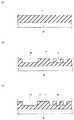
図2(a)に示されるように半導体ウェハW(以下、単に「ウェハ」という。)上に、例えば化学気相成長法(Chemical Vapor Deposition:CVD)或いは塗布法により層間絶縁膜1を形成する(ステップ1A)。層間絶縁膜1の構成材料としては、例えば、有機Si酸化膜、有機樹脂膜及びポーラスSi酸化膜等の低誘電率絶縁膜、SiO2等が挙げられる。As shown in FIG. 2A, an interlayer
層間絶縁膜1を形成した後、図2(b)に示されるようにフォトリソグラフィ技術及び反応性イオンエッチング(RIE)により層間絶縁膜1に、幅が0.3μm以下の細幅配線溝1a及び幅が0.3μmを超える太幅配線溝1bを形成する(ステップ2A)。細幅配線溝1a及び太幅配線溝1bを形成するには、まず、ウェハWを回転させながら層間絶縁膜1上に反射防止膜及び化学増幅型のフォトレジストを塗布する。フォトレジストを塗布した後、所定のパターンが形成されたマスクを使用して、紫外線で露光する。その後、現像液により現像して、層間絶縁膜1上にレジストパターンを形成する。層間絶縁膜1上にレジストパターンを形成した後、レジストパターンをマスクとして、RIEにより層間絶縁膜1をエッチングし、層間絶縁膜1に細幅配線溝1a及び太幅配線溝1bを形成する。層間絶縁膜1に細幅配線溝1a及び太幅配線溝1bを形成した後、アッシング等によりレジスト及び反射防止膜を取り除く。 After the interlayer
層間絶縁膜1に細幅配線溝1a及び太幅配線溝1bを形成した後、図2(c)に示されるように層間絶縁膜1上に、例えばスパッタ法或いはCVD法により層間絶縁膜1への金属拡散を抑制するためのバリアメタル膜2を形成する(ステップ3A)。バリアメタル膜2の構成材料としては、例えばTa、Ti、TaN、TiN、NbN、WN、或いはVN等の導電性材料が挙げられる。なお、これらの材料を積層したものからバリアメタル膜2を形成してもよい。 After forming the
層間絶縁膜1上にバリアメタル膜2を形成した後、図3(a)に示されるようにバリアメタル膜2上に、例えばスパッタ法により電解めっき時に電流を流すためのシード膜3を形成する(ステップ4A)。シード膜3の構成材料としては、例えばCu等の金属が挙げられる。 After the
バリアメタル膜2上にシード膜3を形成した後、図3(b)に示されるようにシード膜3表面にめっき液を供給して、シード膜3上に電解めっき法によりめっき膜(第1の金属膜)4を形成する(ステップ5A)。めっき液には、例えばCuイオンのような金属イオンの他、アクセレーター、サプレッサー、及びレベラー等の添加剤が所定量混入している。また、めっき膜4は、ボトムアップ成膜が顕著な細幅配線溝1a全体に埋め込まれ、かつボトムアップ成膜が起こり難い太幅配線溝1bの一部に埋め込まれるように形成される。めっき膜4は主にCu等の金属から構成されているが、不純物が混入している。ここで、「不純物」とは、S,Cl,O,C,及びNの少なくともいずれかを有する物質である。 After the
シード膜3上にめっき膜4を形成した後、図3(c)に示されるようにめっき膜4上に例えばスパッタ法によりスパッタ膜(第2の金属膜)5を例えば約500nm形成する(ステップ6A)。スパッタ膜5は、高真空中で高純度のターゲットとArガスとを用いて形成することができる。スパッタ膜5は、太幅配線溝1bの他の部分に埋め込まれるように形成される。 After the plating
スパッタ膜5の不純物の濃度(以下、「不純物濃度」という。)は、めっき膜4の不純物濃度よりも低い。ここで、スパッタ膜5の不純物濃度が、めっき膜4の不純物濃度より低いとは、スパッタ膜5中に存在しているS,Cl,O,C,及びNの少なくともいずれかの成分のうち一番濃度の高いものの濃度が、めっき膜4中に存在しているS,Cl,O,C,及びNの少なくともいずれかの成分のうち一番濃度の高いものの濃度よりも低いことをいう。不純物濃度は、例えば、二次イオン質量分析法(Secondary Ion Mass Spectrometry:SIMS)により測定することができる。スパッタ膜5中に存在しているS,Cl,O,C,及びNの少なくともいずれかの成分のうち一番濃度の高いものは、濃度が1.00×10¹⁷atom/cm3以下であることが好ましい。The impurity concentration of the sputtered film 5 (hereinafter referred to as “impurity concentration”) is lower than the impurity concentration of the
なお、本実施の形態では、スパッタ法によりスパッタ膜5を形成しているが、めっき膜4よりも不純物濃度が低い膜を形成することが可能な成膜方法であれば、スパッタ法の代わりに用いてもよい。このような成膜方法としては、例えば、CVD法が挙げられる。 In the present embodiment, the
めっき膜4上にスパッタ膜5を形成した後、ウェハWに熱処理を施し、シード膜3、めっき膜4、及びスパッタ膜5の結晶を成長させて、図4(a)に示されるように配線膜6を形成する(ステップ7A)。ここで、ウェハWに熱処理を加えると、めっき膜4中の不純物がスパッタ膜5中に拡散し、均一化される。熱処理は、例えば150〜300℃で30秒〜60分行われる。 After forming the sputtered
ウェハWに熱処理を施した後、例えば化学的機械的研磨(Chemical Mechanical Polishing:CMP)により研磨して、図4(b)に示されるように細幅配線溝1a及び太幅配線溝1b内に存在するバリアメタル膜2、配線膜6がそれぞれ残るように層間絶縁膜1上の不要なバリアメタル膜2及び配線膜6をそれぞれ除去する(ステップ8A)。具体的には、ウェハWを研磨パッド(図示せず)に接触させた状態で、ウェハW及び研磨パッドを回転させるとともにウェハW上にスラリ(図示せず)を供給して、配線膜6等を研磨する。なお、CMPで研磨する場合に限らず、その他の手法で研磨してもよい。その他の手法としては、例えば電解研磨が挙げられる。 After the heat treatment is performed on the wafer W, the wafer W is polished by, for example, chemical mechanical polishing (CMP) so as to be formed in the
これにより、線幅が0.3μm以下の細幅配線(第1の配線)6aと、線幅が0.3μmを超える太幅配線(第2の配線)6bとが形成される。このとき、得られた太幅配線6bの不純物濃度は、細幅配線6aの不純物濃度よりも低くなっている。これは、細幅配線6aがシード膜2とめっき膜4とから形成されたのに対し、太幅配線6bはシード膜2とめっき膜4とめっき膜4よりも不純物濃度が低いスパッタ膜5とから形成されたからである。 As a result, narrow wiring (first wiring) 6a having a line width of 0.3 μm or less and thick wiring (second wiring) 6b having a line width exceeding 0.3 μm are formed. At this time, the impurity concentration of the obtained
ここで細幅配線6a及び太幅配線6bそれぞれの不純物濃度としては、細幅配線6aで5×10¹⁸atom/cm3〜1×1019atom/cm3程度、太幅配線6bで5×1018atom/cm3未満程度とすることが好ましい。即ち、細幅配線6aの不純物濃度が低すぎると、不純物による配線中の空孔のピンニングをさほど期待できず、細幅配線6a及び太幅配線6bの不純物濃度がそれぞれ上記範囲を逸脱して高すぎると、不純物凝集起因の欠陥発生の可能性が増大する。本実施の形態においては、例えば、めっき成膜時におけるボトムアップ成長が顕著な配線幅0.05μm以上0.3μm以下の細幅配線6aの不純物濃度を5×1018atom/cm3〜1×1019atom/cm3、この細幅配線6aと同一面に形成される配線幅0.3μmを越えて10μm以下の太幅配線6bの不純物濃度を5×1018atom/cm3未満に設定すればよい。なお、ここでの不純物濃度についても、細幅配線6a内及び太幅配線6b内のそれぞれに存在しているS,Cl,O,C,及びNの少なくともいずれかの成分のうち、一番濃度の高いものの濃度で定義すればよい。Here, the impurity concentration of each of the narrow wiring 6a and the
本実施の形態によれば、太幅配線溝1b内の不純物濃度を低下させることができるので、欠陥の少ない太幅配線6bを形成することができる。太幅配線溝1b内に不純物が存在すると欠陥が生じるのは、次のような理由からであると考えられる。即ち、ボトムアップ成長が顕著な細幅配線溝1a内においては、めっき膜4の成膜速度が速いために添加剤が過剰に供給されても不純物濃度は増大しないが、ボトムアップ成長が起こり難くなる太幅配線溝1b内においては不純物濃度が増大する。この結果、熱処理工程における結晶成長の進行に伴い、太幅配線溝1b内の不純物が凝集した部分に欠陥が生じてしまうものと考えられる。 According to the present embodiment, since the impurity concentration in the
本実施の形態では、めっき膜4上にめっき膜4よりも不純物濃度が低いスパッタ膜5を形成しているので、熱処理工程においてめっき膜4中の不純物をスパッタ膜5中に拡散させることができる。これにより太幅配線溝1b内の不純物濃度を低下させることができ、欠陥の少ない太幅配線6bを形成することができるので、配線の信頼性が向上した半導体装置を提供することができる。 In the present embodiment, since the sputtered
さらに本実施の形態によれば、太幅配線溝1bの一部に埋め込まれるようにめっき膜4を形成し、その後太幅配線溝1bの他の部分に埋め込まれるようにスパッタ膜5を形成しているので、めっき膜4が太幅配線溝1b全体に埋め込まれた場合に比べて、太幅配線溝1b内の不純物を低減させることができる。これにより、より欠陥の少ない太幅配線6bを形成することができる。 Furthermore, according to the present embodiment, the
一方本実施の形態によれば、細幅配線溝1aの幅が0.3μm以下であり、かつ細幅配線溝1a全体にめっき膜4が埋め込まれているので、ボトムアップ成膜により細幅配線溝1a内を確実に埋め込むことができる。なお、ボトムアップ成膜は、幅が0.3μm以下の溝で顕著に起こるものと考えられる。また、このような細幅配線6aにおいては細幅配線溝1aの幅以下に結晶成長の進行が制限されるため、結晶成長に伴う不純物凝集に起因する欠陥発生の可能性は小さい。 On the other hand, according to the present embodiment, since the width of the
むしろ、本実施の形態によれば、不純物を細幅配線6a中にある程度存在させることで、細幅配線6a中の空孔をピンニングさせることができ、空孔が細幅配線6a中をマイグレーションするのを抑制することができる。これにより、断線若しくは抵抗上昇の原因となる配線中の大きなボイド生成を抑制することができ、配線の信頼性を向上させた半導体装置を提供することができる。 Rather, according to the present embodiment, by allowing impurities to exist to some extent in the narrow wiring 6a, the holes in the narrow wiring 6a can be pinned, and the holes migrate in the narrow wiring 6a. Can be suppressed. As a result, it is possible to suppress the generation of large voids in the wiring that cause disconnection or increase in resistance, and it is possible to provide a semiconductor device with improved wiring reliability.
(実験例1)
以下、実験例1について説明する。本実験例では、Cu膜中の不純物濃度を測定するとともにCu配線中の欠陥密度を測定した。(Experimental example 1)
Hereinafter, Experimental Example 1 will be described. In this experimental example, the impurity concentration in the Cu film was measured and the defect density in the Cu wiring was measured.
本実験においては、次のような工程で形成されたウェハを使用した。能動部を有するSi基板に酸化膜を20nm形成した後、CVD法によりSiOC系の低誘電率絶縁膜(層間絶縁膜)を300nm形成した。その後リソグラフィー工程及びRIE工程により、幅4μm及び深さ250nmの配線溝(太幅配線溝)を形成した。そして、ウエットエッチング工程によりレジスト除去を行った後、ロングスロースパッタ法によりTa膜(バリアメタル膜)とCu膜(シード膜)をそれぞれ30nm及び80nm形成した。次に、2種類の成膜方法により、Cu膜を形成した。条件1では、電解めっき法により1A/ウェハの電流条件でCu膜(めっき膜)を210nm形成した。また条件2では、電解めっき法により1A/ウェハの電流条件でCu膜(めっき膜)を10nm形成した後、ロングスロースパッタ法によりCu膜(スパッタ膜)を200nm形成した。そして、これらのウェハを水素濃度約10vol%のフォーミングガス中にて270℃で40分熱処理し、その後CMPにより不要なCu膜等を除去して、Cu配線を形成した。 In this experiment, a wafer formed by the following process was used. An oxide film having a thickness of 20 nm was formed on a Si substrate having an active portion, and a SiOC-based low dielectric constant insulating film (interlayer insulating film) was formed by CVD to a thickness of 300 nm. Thereafter, a wiring groove (thick wiring groove) having a width of 4 μm and a depth of 250 nm was formed by a lithography process and an RIE process. Then, after removing the resist by a wet etching process, a Ta film (barrier metal film) and a Cu film (seed film) were formed to 30 nm and 80 nm, respectively, by a long throw sputtering method. Next, a Cu film was formed by two kinds of film forming methods. In
そして、このようなウェハを使用して、Cu膜中の不純物の濃度を測定するとともにCu配線の欠陥密度を測定した。不純物濃度の測定は、CMPにより不要なCu膜等が除去される前のCu膜中のCl,O,Cの濃度をそれぞれSIMSで測定することにより行われた。また、欠陥密度の測定は、Cu配線の欠陥密度をそれぞれ欠陥検査装置で測定することにより行われた。 And using such a wafer, while measuring the density | concentration of the impurity in Cu film | membrane, the defect density of Cu wiring was measured. The impurity concentration was measured by measuring the concentrations of Cl, O, and C in the Cu film before removal of unnecessary Cu film and the like by CMP, respectively, by SIMS. The defect density was measured by measuring the defect density of the Cu wiring with a defect inspection device.
以下、結果を述べる。表1は条件1及び条件2におけるCu膜中の不純物濃度とCu配線中の欠陥密度を表したものである。
表1に示されるように通常の条件である条件1に比べ、条件2ではCu膜中の不純物濃度が約3桁近く減少していた。また、それに伴いCu配線中の欠陥密度が激減していた。これらの結果から、めっき法によりCu膜を形成した後スパッタ法によりCu膜を形成した場合には、Cu膜中の不純物濃度が低下することが確認され、またCu配線中の欠陥密度が低下することが確認された。なお本実験例ではCu配線について記載したが、Ag配線やAu配線についても、Agめっき膜、Auめっき膜上にそれぞれAgスパッタ膜、Auスパッタ膜等を形成することにより同様の効果を得ることができる。 As shown in Table 1, the impurity concentration in the Cu film was reduced by about three orders of magnitude in
(第2の実施の形態)
以下、第2の実施の形態について説明する。本実施の形態では、めっき液を15L/min以上の供給速度で供給するとともにウェハを50rpm以下の回転数で回転させながらめっき膜を形成する例について説明する。(Second Embodiment)
Hereinafter, a second embodiment will be described. In the present embodiment, an example in which a plating film is formed while supplying a plating solution at a supply speed of 15 L / min or more and rotating the wafer at a rotation speed of 50 rpm or less will be described.
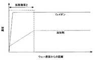
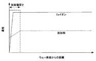
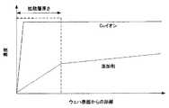
図5は、本実施の形態に係る半導体装置の製造プロセスの流れを示したフローチャートであり、図6は本実施の形態に係る半導体装置の模式的な製造プロセス図であり、図7は本実施の形態に係るめっき膜の模式的な形成プロセス図であり、図8はめっき液を15L/min以上の供給速度で供給するとともにウェハを50rpm以下の回転数で回転させてめっきを施している場合におけるCuイオン及び添加剤の濃度とウェハ表面からの距離との関係を表したものであり、図9はめっき液を15L/min以上の供給速度で供給するとともにウェハを100rpm程度の回転数で回転させてめっきを施している場合におけるCuイオン及び添加剤の濃度とウェハ表面からの距離との関係を表したものであり、図10はめっき液を15L/min未満の供給速度で供給するとともにウェハを50rpm以下の回転数で回転させてめっきを施している場合におけるCuイオン及び添加剤の濃度とウェハ表面からの距離との関係を表したものである。 FIG. 5 is a flowchart showing the flow of the manufacturing process of the semiconductor device according to the present embodiment, FIG. 6 is a schematic manufacturing process diagram of the semiconductor device according to the present embodiment, and FIG. FIG. 8 is a schematic process diagram for forming a plating film according to the embodiment, and FIG. 8 is a case where plating is performed by supplying a plating solution at a supply speed of 15 L / min or more and rotating the wafer at a rotation speed of 50 rpm or less. FIG. 9 shows the relationship between the concentration of Cu ions and additives and the distance from the wafer surface in FIG. 9. FIG. 9 supplies the plating solution at a supply speed of 15 L / min or more and rotates the wafer at a rotation speed of about 100 rpm. FIG. 10 shows the relationship between the concentration of Cu ions and additives and the distance from the wafer surface when plating is performed, and FIG. 10 shows the plating solution at 15 L / m. Supplies at a feed rate of less than n illustrates a relationship between a distance from the density and the wafer surface of the Cu ions and additives in a case where plated by rotating the wafer at the following rotation speed 50 rpm.
図5に示されるように、ウェハW上に、層間絶縁膜1を形成する(ステップ1B)。層間絶縁膜1を形成した後、フォトリソグラフィ技術及び反応性イオンエッチング(RIE)により層間絶縁膜1に細幅配線溝1a及び太幅配線溝1bを形成する(ステップ2B)。 As shown in FIG. 5, an
層間絶縁膜1に細幅配線溝1a及び太幅配線溝1bを形成した後、層間絶縁膜1上に、バリアメタル膜2を形成する(ステップ3B)。層間絶縁膜1上にバリアメタル膜2を形成した後、バリアメタル膜2上にシード膜3を形成する(ステップ4B)。 After the
バリアメタル膜2上にシード膜3を形成した後、シード膜3表面にめっき液を供給して、図6に示されるように電解めっき法によりめっき膜4を形成する(ステップ5B)。本実施の形態では、めっき膜4は、細幅配線溝1a全体及び太幅配線溝1b全体に埋め込まれるように形成される。 After the
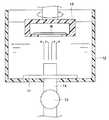
めっき膜4を形成するには、まず、図7に示されるようにシード膜3が下面となるようにウェハWをホルダ10に保持させた状態で、ウェハWをカソードとしてウェハWとアノード11との間に電圧を印加する。その後、ウェハWを傾けるとともにめっき液槽12内で15L/min以上の供給速度で噴流しているめっき液にウェハWを浸漬する。このとき、ウェハ表面への泡吸着を抑制するためにウェハWを回転させることが好ましいが、浸漬方法を工夫する等により泡吸着を抑制可能であれば、ウェハWを回転しない状態でめっき液に浸漬しても構わない。 In order to form the
続いて、ウェハWがめっき液に浸漬した状態では、めっき液の供給速度を15L/min以上に、かつウェハWの回転数を50rpm以下に維持しておく。これにより、細幅配線溝1a及び太幅配線溝1bを埋め込むようにめっき膜4が形成される。ここで、ウェハWの回転数はめっき成膜中常に一定である必要はなく、50rpm以下の範囲で変化させてもよいし、あるいはウェハWの回転が止められることがあってもよい。即ち、細幅配線溝1a及び太幅配線溝1bの少なくとも一部がめっき膜4で埋め込まれる際に、めっき液を15L/min以上の供給速度で供給するとともにウェハWを50rpm以下の回転数で回転させてめっきを施せばよい。なお、めっき液の供給速度は、めっき液を汲み出すポンプ13或いはポンプ13より汲み出されためっき液をめっき液槽12に供給するための供給管14等に設置された流量計(図示せず)により測定することができる。 Subsequently, in a state where the wafer W is immersed in the plating solution, the supply rate of the plating solution is maintained at 15 L / min or more and the rotation speed of the wafer W is maintained at 50 rpm or less. Thus, the
また本実施の形態では、電圧を印加した状態でウェハWを浸漬する、いわゆるホットエントリー法を用いており浸漬した部分からめっきが開始するため、浸漬時のウェハWの回転数も50rpm以下にすることが好ましい。これまでウェハWを低い回転数で回転させながらウェハWをめっき液に接触させた場合には、ウェハWの表面に気泡が形成され、めっき膜4の面内均一性が低下すると考えられていたが、実験によりウェハWを0rpmを超え50rpm以下の回転数で回転させながらめっき液にウェハWを接触させた場合であっても気泡の形成を抑え得ることが判明した。これにより、めっき膜4の面内均一性の低下を抑制することができる。 In this embodiment, since the so-called hot entry method in which the wafer W is immersed in a state where a voltage is applied is used and plating starts from the immersed portion, the number of rotations of the wafer W during immersion is set to 50 rpm or less. It is preferable. In the past, when the wafer W was brought into contact with the plating solution while rotating the wafer W at a low rotation speed, bubbles were formed on the surface of the wafer W, and the in-plane uniformity of the
シード膜3上にめっき膜4を形成した後、ウェハWに熱処理を施し、シード膜3及びめっき膜4の結晶を成長させて、配線膜6を形成する(ステップ6B)。 After the
配線膜6を形成した後、例えばCMPにより研磨して、細幅配線溝1a及び太幅配線溝1b内に存在するバリアメタル膜2及び配線膜6がそれぞれ残るように層間絶縁膜1上の不要なバリアメタル膜2及び配線膜6をそれぞれ除去する(ステップ7B)。これにより、線幅が0.3μm以下の細幅配線6aと、線幅が0.3μmを超える太幅配線6bとが形成される。 After the
本実施の形態によれば、太幅配線溝1b内の不純物濃度を低下させることができるので、欠陥の少ない太幅配線6bを形成することができる。また、添加剤の効果を得ることができるので、ボトムアップ成膜により細幅配線溝1a内にめっき膜4を埋め込むことができる。即ち、ウェハWを回転させると、ウェハWの表面には拡散層が形成される。拡散層の厚さは回転電極についてはLevichの次式(1)で表される。 According to the present embodiment, since the impurity concentration in the
δ=1.61D01/3ν1/6ω−1/2 …(1)
ここで、D0は拡散係数、νは溶液の粘性率、ωは角速度である。この式により、ウェハを低回転にすればするほど、拡散層の厚さδは厚くなることが分かる。δ = 1.61D01/3 ν1/6 ω−1/2 (1)
Here, D0 is the diffusion coefficient, ν is the viscosity of the solution, and ω is the angular velocity. From this equation, it can be seen that the lower the rotation of the wafer, the thicker the diffusion layer thickness δ.
めっき初期においては最小線幅での埋め込み性を確保するために、電流密度は10mA/cm2程度に調節されている。この条件下ではめっき液中のCuイオンは十分に存在するため反応律速状態にある。そのため拡散層内においてもCuイオンの濃度(Cuイオン濃度)はほぼ一定と考えることができる。これに対し、添加剤は微量で効果をもたらすため、めっき液中の添加剤の濃度(添加剤濃度)はCuイオンに比べて非常に小さく、ウェハW表面では拡散律速状態にある。そのため拡散層内における添加剤濃度はほぼ直線的な濃度勾配ができていると考えることができる。In the initial stage of plating, the current density is adjusted to about 10 mA / cm2 in order to ensure embeddability with the minimum line width. Under these conditions, Cu ions in the plating solution are sufficiently present, so that they are in a reaction rate limiting state. Therefore, it can be considered that the concentration of Cu ions (Cu ion concentration) is almost constant also in the diffusion layer. On the other hand, since the additive brings about an effect in a very small amount, the concentration of the additive (additive concentration) in the plating solution is very small as compared with Cu ions, and the surface of the wafer W is in a diffusion-controlled state. Therefore, it can be considered that the additive concentration in the diffusion layer has a substantially linear concentration gradient.
図9に示されるようにウェハWの回転数が100rpm程度の場合には、拡散層の厚さが薄くなり、ウェハW表面付近における添加剤濃度は高くなってしまうので、めっき膜4中における不純物濃度が高くなってしまう。これに対し、図8及び図10に示されるようにウェハWの回転数が50rpm以下の場合には、拡散層の厚さが厚くなり、ウェハW表面付近における添加剤濃度が低くなる。これにより、めっき膜4中に取り込まれる添加剤量が低減するので、めっき膜4中の不純物濃度を低下させることができる。それ故、欠陥の少ない太幅配線6bを形成することができる。 As shown in FIG. 9, when the rotation speed of the wafer W is about 100 rpm, the thickness of the diffusion layer becomes thin and the additive concentration near the surface of the wafer W becomes high. The concentration becomes high. On the other hand, as shown in FIGS. 8 and 10, when the rotation speed of the wafer W is 50 rpm or less, the thickness of the diffusion layer is increased, and the additive concentration in the vicinity of the surface of the wafer W is decreased. Thereby, since the amount of the additive taken into the
しかしながら、めっき液の供給速度が15L/min未満であると、めっき液槽12内に貯留されためっき液中ではウェハW表面での添加剤の吸着が進み、図10に示されるように拡散層外の添加剤濃度が低下してしまうため、結果としてウェハW表面の添加剤濃度が必要量を下回り添加剤の効果が得られなくなってしまう。これに対し、めっき液を15L/min以上の供給速度で供給した場合には、添加剤は拡散層内において拡散律速となり、図8に示されるように拡散層外の添加剤濃度をほぼ一定に保つことができる。これにより、添加剤の効果を得ることができ、ボトムアップ成膜により細幅配線溝1a内にめっき膜4を埋め込むことができる。 However, if the supply rate of the plating solution is less than 15 L / min, the adsorption of the additive on the surface of the wafer W proceeds in the plating solution stored in the
(実験例2)
以下、実験例2について説明する。本実験例では、細幅配線及び太幅配線の欠陥密度を測定するとともに太幅配線の信頼性試験を行った。また、ウェハをめっき液に接触させたときのウェハの表面状態を観察した。(Experimental example 2)
Hereinafter, Experimental Example 2 will be described. In this experimental example, the defect density of the narrow wiring and the wide wiring was measured, and the reliability test of the thick wiring was performed. Moreover, the surface state of the wafer when the wafer was brought into contact with the plating solution was observed.
本実験例では、第2の実施の形態で説明した手順により0.09μmの細幅配線及び0.5μmの太幅配線を有する300mmのウェハを複数枚作成し、それぞれのウェハについて細幅配線と太幅配線の欠陥密度を測定するとともに太幅配線の信頼性試験を行った。ここで、めっき膜の形成は、めっき液の供給速度を20L/minとして、ウェハ毎にウェハの回転数が異なった状態で行われた。また、めっき膜を形成する際に、ウェハをめっき液に接触させたときのウェハの表面状態をそれぞれ観察した。 In this experimental example, a plurality of 300 mm wafers having 0.09 μm narrow wiring and 0.5 μm thick wiring were prepared by the procedure described in the second embodiment. The defect density of the wide wiring was measured and the reliability test of the wide wiring was performed. Here, the formation of the plating film was performed in a state where the supply speed of the plating solution was 20 L / min and the wafer rotation speed was different for each wafer. Further, when the plating film was formed, the surface state of the wafer when the wafer was brought into contact with the plating solution was observed.
以下、結果を述べる。図11は実験例2に係るウェハの回転数と欠陥密度との関係を示すグラフである。図11に示されるように細幅配線においてはウェハの回転数を変えた場合であってもほぼ欠陥密度は変化しないが、太幅配線においてはウェハの回転数が低いほど欠陥密度が低い。この結果から、細幅配線はウェハの回転数にほぼ影響を受けないが、太幅配線はウェハの回転数が低いほど好ましいということが確認された。また、太幅配線に対しての信頼性試験に関しても、ウェハの回転数が低いほど好ましいことが確認された。 The results are described below. FIG. 11 is a graph showing the relationship between the wafer rotation speed and the defect density according to Experimental Example 2. As shown in FIG. 11, in the narrow wiring, even if the rotation speed of the wafer is changed, the defect density is not substantially changed, but in the thick wiring, the defect density is lower as the rotation speed of the wafer is lower. From this result, it was confirmed that the narrow wiring is almost unaffected by the rotation speed of the wafer, but the thick wiring is preferable as the rotation speed of the wafer is low. In addition, regarding the reliability test for the thick wiring, it was confirmed that the lower the rotation speed of the wafer, the better.
さらに、ウェハをめっき液に接触させたときのウェハの表面状態に関しては、気泡がほぼ形成されていなかった。この結果から、ウェハを0rpmを超え50rpm以下で回転させながらウェハをめっき液に接触させた場合であっても、めっき膜の面内均一性の低下を抑制できることが確認された。 Furthermore, regarding the surface state of the wafer when the wafer was brought into contact with the plating solution, almost no bubbles were formed. From this result, it was confirmed that even when the wafer was brought into contact with the plating solution while rotating the wafer at more than 0 rpm and not more than 50 rpm, a decrease in in-plane uniformity of the plating film could be suppressed.
(第3の実施の形態)
以下、第3の実施の形態について説明する。本実施の形態では、バリアメタル膜を、2A族、4A族、5A族、6A族、及び2B族のいずれかの族に属し、かつめっき膜の主成分の金属と反応物を形成し得る金属から構成した例について説明する。なお、第1の実施の形態と重複する内容については省略することもある。(Third embodiment)
The third embodiment will be described below. In the present embodiment, the barrier metal film belongs to any one of groups 2A, 4A, 5A, 6A, and 2B, and can form a reactant with the main component metal of the plating film. An example constructed from the above will be described. Note that the same contents as those in the first embodiment may be omitted.
図12(a)〜図15(c)は本実施の形態に係る半導体装置の模式的な製造プロセス図である。図16(a)は本実施の形態に係る太幅配線の主成分がCuであり、バリアメタル膜がTiから構成されている場合における太幅配線とバリアメタル膜との界面の様子を模式的に示した図であり、図16(b)は参考例に係る太幅配線の主成分がCuであり、バリアメタル膜がTaから構成されている場合における太幅配線とバリアメタル膜との界面の様子を模式的に示した図である。 FIG. 12A to FIG. 15C are schematic manufacturing process diagrams of the semiconductor device according to the present embodiment. FIG. 16A schematically illustrates the interface between the thick wiring and the barrier metal film when the main component of the thick wiring according to the present embodiment is Cu and the barrier metal film is made of Ti. FIG. 16B shows the interface between the thick wiring and the barrier metal film when the main component of the thick wiring according to the reference example is Cu and the barrier metal film is made of Ta. It is the figure which showed the mode of.
図12(a)に示されるように図示しない下層電極が露出するSiO2膜21上に、層間絶縁膜22を形成する。本実施の形態では、層間絶縁膜22は、有機系低誘電率絶縁膜であるポリアリーレンエーテル膜23(以下、「PAE膜」という。)と、PAE膜23上に形成されたSiO2膜24とから構成されている。SiO2膜24は、CMPの際における保護膜としても機能する。なお、本実施の形態では、層間絶縁膜22としてPAE膜23及びSiO2膜24を使用しているが、これらに限定されず、例えば上記第1の実施の形態で説明した層間絶縁膜1を使用することも可能である。As shown in FIG. 12A, an
ウェハW上に層間絶縁膜22を形成した後、図12(b)に示されるようにフォトリソグラフィ技術及び反応性イオンエッチング(RIE)により層間絶縁膜22に幅が0.3μm以下の細幅配線溝22a及び幅が0.3μmを超える太幅配線溝22bを形成する。 After forming the
層間絶縁膜22に細幅配線溝22a及び太幅配線溝22bを形成した後、図12(c)に示されるように層間絶縁膜22上にバリアメタル膜25を形成する。バリアメタル膜25は、2A族、4A族、5A族、6A族、及び2B族のいずれかの族に属し、かつ後述するめっき膜27の主成分の金属と反応物を形成し得る金属から選択された1以上の金属から構成されている。2A族、4A族、5A族、6A族、及び2B族のいずれかの族に属し、かつめっき膜27の主成分の金属と反応物を形成し得る金属としては、例えば、Mg、Ti、V、Zn、Zr、Hf、及びWから選択された1以上の金属が挙げられる。これらの金属の中でも、Tiが好ましい。 After the
層間絶縁膜22上にバリアメタル膜25を形成した後、図12(c)に示されるようにバリアメタル膜25上にシード膜26を形成する。シード膜26はバリアメタル膜25と直接接するように形成され、まためっき膜27と同一の金属を主成分としている。 After forming a
バリアメタル膜25上にシード膜26を形成した後、シード膜26表面にめっき液を供給するとともにシード膜26に電流を供給して、図12(d)に示されるように電解めっき法によりめっき膜(第1の金属膜)27を形成する。本実施の形態では、めっき膜27は、細幅配線溝22a全体及び太幅配線溝22bの一部に埋め込まれるように形成される。めっき膜27を構成する主成分の金属としては、例えば、Cu、Ag、Auの少なくともいずれかが挙げられる。 After the
シード膜26上にめっき膜27を形成した後、図13(a)に示されるようにめっき膜27上に例えばスパッタ法によりスパッタ膜(第2の金属膜)28を形成する。スパッタ膜28は、太幅配線溝22bの他の部分に埋め込まれるように形成される。スパッタ膜28は、めっき膜27と同一の金属を主成分とし、不純物濃度がめっき膜27の不純物濃度より低い。 After forming the
めっき膜27上にスパッタ膜28を形成した後、ウェハWに熱処理を施し、シード膜26、めっき膜27、及びスパッタ膜28の結晶を成長させて、図13(b)に示されるように配線膜29を形成する。 After forming the sputtered
配線膜29を形成した後、例えばCMPにより研磨して、図13(c)に示されるように細幅配線溝22a及び太幅配線溝22b内に存在するバリアメタル膜25及び配線膜29がそれぞれ残るように層間絶縁膜22上の不要なバリアメタル膜25及び配線膜29をそれぞれ除去する。これにより、線幅が0.3μm以下の細幅配線(第1の配線)29aと、線幅が0.3μmを超える太幅配線(第2の配線)29bとを有する第1層配線が形成される。 After the
細幅配線29aと太幅配線29bを形成した後、図13(d)に示されるように層間絶縁膜22上にRIEのストッパー膜及びCuの拡散防止膜としてのSiCN膜31、層間絶縁膜32を順次形成する。層間絶縁膜32は、無機系低誘電率絶縁膜であるSiCO膜33と、SiCO膜33上に形成された有機系低誘電率絶縁膜であるPAE膜34と、PAE膜34上に形成されたSiO2膜35とから構成されている。SiO2膜35は、CMPの保護膜としても機能する。After forming the
層間絶縁膜22上にSiCN膜31等を形成した後、図14(a)に示されるようにフォトリソグラフィ技術及び反応性イオンエッチング(RIE)により層間絶縁膜32にビアホール32a、細幅配線溝32b、太幅配線溝32cを形成する。 After the
その後、図14(b)に示されるように層間絶縁膜32上にバリアメタル膜36を形成する。バリアメタル膜36は、バリアメタル膜25と同様の金属から構成されている。 Thereafter, a
層間絶縁膜32上にバリアメタル膜36を形成した後、図14(b)に示されるようにバリアメタル膜36上にシード膜37を形成する。シード膜37はバリアメタル膜36と直接接するように形成され、また後述するめっき膜38と同一の金属を主成分としている。 After the
バリアメタル膜36上にシード膜37を形成した後、シード膜37表面にめっき液を供給するとともにシード膜37に電流を供給して、図14(c)に示されるように電解めっき法によりめっき膜(第1の金属膜)38を形成する。本実施の形態では、めっき膜38は、ビアホール32a全体、細幅配線溝32b全体、及び太幅配線溝32cの一部に埋め込まれるように形成される。めっき膜38を構成する主成分の金属としては、めっき膜27を構成している主成分の金属と同一の金属が挙げられる。 After the
シード膜37上にめっき膜38を形成した後、図15(a)に示されるようにめっき膜38上に例えばスパッタ法によりスパッタ膜(第2の金属膜)39を形成する。スパッタ膜39は、太幅配線溝32cの他の部分に埋め込まれるように形成される。スパッタ膜39は、めっき膜38と同一の金属を主成分とし、不純物濃度がめっき膜38の不純物濃度より低い。 After the
めっき膜38上にスパッタ膜39を形成した後、ウェハWに熱処理を施し、シード膜37、めっき膜38、及びスパッタ膜39の結晶を成長させて、図15(b)に示されるように配線膜40を形成する。 After forming the sputtered
配線膜40を形成した後、例えばCMPにより研磨して、図15(c)に示されるようにビアホール32a、細幅配線溝32b、及び太幅配線溝32c内に存在するバリアメタル膜36及び配線膜40がそれぞれ残るように層間絶縁膜32上の不要なバリアメタル膜36及び配線膜40をそれぞれ除去する。これにより、第1層配線とビアプラグ40aで接続され、線幅が0.3μm以下の細幅配線(第1の配線)40bと線幅が0.3μmを超える太幅配線(第2の配線)40cを備える第2層配線が形成される。なお、3層以上の配線を形成する場合には、これらの工程を繰返すことにより実現することができる。 After forming the
デュアルダマシン構造においてビアプラグの直下に欠陥が存在する場合、イールドが劣化し、またマイクロボイド起因によりエレクトロマイグレーション(EM)の耐性が劣化してしまう。上記第1の実施の形態に記載した手法によりこれらを改善することができるが、配線幅や深さが多様に存在する実際のパターンにおいては、その反面、ストレスマイグレーション(SM)の信頼性が劣化したパターンが存在するおそれがある。 In the dual damascene structure, when a defect exists directly under the via plug, the yield deteriorates, and the resistance to electromigration (EM) deteriorates due to microvoids. Although these can be improved by the method described in the first embodiment, the reliability of stress migration (SM) is deteriorated in the actual pattern having various wiring widths and depths. There is a possibility that the pattern has existed.
即ち、配線中の不純物濃度が低すぎると、スパッタ膜形成後の熱処理時のみならず、後工程におけるMOSFET(Metal Oxide Semiconductor Field Effect Transistor)のゲート絶縁膜の欠陥準位を回復させる熱処理等を行った際においても、配線中の金属原子が拡散移動して、金属粒の粒径が更に変化してしまうおそれがある。これは、配線中の不純物濃度が低いことにより、金属原子の拡散移動を阻害する要因が低減するためである。これにより、ストレスマイグレーション(SM)信頼性が劣化すると考えられる。この現象は、特に不純物濃度が低い太幅配線で起こり易い。 That is, if the impurity concentration in the wiring is too low, not only the heat treatment after the formation of the sputtered film but also the heat treatment that recovers the defect level of the gate insulating film of the MOSFET (Metal Oxide Semiconductor Field Effect Transistor) in the subsequent process. Even in this case, the metal atoms in the wiring may diffuse and move, and the particle size of the metal particles may further change. This is because the factor that inhibits the diffusion movement of metal atoms is reduced due to the low impurity concentration in the wiring. This is considered to degrade the stress migration (SM) reliability. This phenomenon is likely to occur particularly with a wide wiring having a low impurity concentration.
これに対し、本実施の形態では、バリアメタル膜25を、2A族、4A族、5A族、6A族、及び2B族のいずれかの族に属し、かつめっき膜27の主成分の金属と反応物を形成し得る金属から構成しているので、太幅配線29bの主成分である金属とバリアメタル膜25を構成している金属とが相互拡散し、太幅配線29bとバリアメタル膜25との界面に、太幅配線29bの主成分である金属とバリアメタル膜25を構成する金属との反応物を含む原子レベルの拡散層が形成される。具体的には、例えば、太幅配線29bの主成分がCuであり、バリアメタル膜25がTiから構成されている場合には、図16(a)に示されるように太幅配線29bとバリアメタル膜25との界面にCuとTiとの反応物を含む拡散層30が形成される。このような反応物を含む拡散層30が形成されることにより、太幅配線29bとバリアメタル膜25との密着性が向上し、太幅配線29bとバリアメタル膜25との界面における金属原子の拡散移動が抑制される。それ故、太幅配線29b内の不純物濃度が低い場合であっても、ストレスマイグレーション信頼性の劣化を抑制することができ、結果として配線におけるストレスマイグレーション信頼性の劣化の抑制及び欠陥の低減の両立を図ることができる。一方、太幅配線29bの主成分がCuであり、バリアメタル膜がめっき膜27の主成分の金属と反応物を形成し得ない金属であるTaから構成されている場合には、図16(b)に示されるように太幅配線29bとバリアメタル膜101との界面にはCuとTaの反応物を含む拡散層は形成されず、上記のような効果は得られない。 On the other hand, in the present embodiment, the
なお、太幅配線29bとバリアメタル膜25との界面以外にも、細幅配線29aとバリアメタル膜25との界面、ビアプラグ40aとバリアメタル膜36との界面、細幅配線40bとバリアメタル膜36との界面、太幅配線40cとバリアメタル膜36との界面においても上記のような反応物を含む拡散層が形成されるので、上記と同様の効果が得られる。 In addition to the interface between the
本実施の形態では、2A族、4A族、5A族、6A族、及び2B族のいずれかの族に属し、かつめっき膜27,38の主成分の金属と反応物を形成し得る金属から構成されたバリアメタル膜25,36を使用しているが、これらの金属を含み、かつシード層26,37と直接接触するような膜であればバリアメタル膜でなくともよい。 In the present embodiment, it is composed of a metal that belongs to any of the 2A group, 4A group, 5A group, 6A group, and 2B group and that can form a reactant with the main component metal of the plating
また、バリアメタル膜25,36は、2A族、4A族、5A族、6A族、及び2B族のいずれかの族に属し、かつめっき膜27,38の主成分の金属と反応物を形成し得る金属を含んでいれば、その他、めっき膜27,38の主成分の金属と反応物を形成し得ない金属を含んでいてもよい。めっき膜27,38の主成分の金属と反応物を形成し得ない金属としては、例えばTa、TaN等が挙げられる。 Further, the
さらに、バリアメタル膜25がシード膜26に、或いはバリアメタル膜36がシード膜37に直接接するように形成されれば、層間絶縁膜22とバリアメタル膜25との間、或いは層間絶縁膜32とバリアメタル膜36との間に他のバリアメタル膜を形成してもよい。ここで、他のバリアメタル膜は、めっき膜27,38及びスパッタ膜28,39の主成分の金属と反応物を形成し得ない金属から構成されていてもよい。この場合、第1層配線と第2層配線が形成された状態においては、層間絶縁膜22,32と太幅配線29b,40cとの間には太幅配線29b,40c側にバリアメタル膜25,36、層間絶縁膜22,32側に他のバリアメタル膜が形成されている。 Furthermore, if the
なお、本発明は上記実施の形態の記載内容に限定されるものではなく、構造や材質、各部材の配置等は、本発明の要旨を逸脱しない範囲で適宜変更可能である。例えば、第1及び第2の実施の形態においては、配線は多層構造のものではないが、第3の実施の形態のように多層構造のものであってもよく、また逆に第3の実施の形態においては、配線は多層構造のものでなくともよい。 The present invention is not limited to the description of the above embodiment, and the structure, material, arrangement of each member, and the like can be appropriately changed without departing from the gist of the present invention. For example, in the first and second embodiments, the wiring is not of a multilayer structure, but may be of a multilayer structure as in the third embodiment, and conversely the third implementation. In this embodiment, the wiring may not have a multilayer structure.
W…ウェハ、1,22,32…層間絶縁膜、1a,22a,32b…細幅配線溝、1b,22b,32c…太幅配線溝、4,27,38…めっき膜、5,28,39…スパッタ膜、6,29,40…配線膜、6a,29a,40b…細幅配線、6b,29b,40c…太幅配線、32a…ビアホール、40a…ビアプラグ。 W ... wafer, 1, 22, 32 ... interlayer insulating film, 1a, 22a, 32b ... narrow wiring groove, 1b, 22b, 32c ... thick wiring groove, 4, 27, 38 ... plating film, 5, 28, 39 ... sputtered film, 6, 29, 40 ... wiring film, 6a, 29a, 40b ... narrow wiring, 6b, 29b, 40c ... thick wiring, 32a ... via hole, 40a ... via plug.
Claims (5)
Translated fromJapanese前記第1の金属膜上に前記めっき法とは異なる成膜方法により、前記第1の金属膜と同一の金属を主成分とし、不純物の濃度が前記第1の金属膜の不純物の濃度より低い第2の金属膜を形成する工程と、
前記第1及び第2の金属膜に熱処理を施す工程と、
前記熱処理を施した後に、前記凹部に埋め込まれた部分以外の第1及び第2の金属膜を除去する工程と
を具備することを特徴とする半導体装置の製造方法。Forming a first metal film by plating so as to be embedded in at least a part of the recess on a substrate having a recess formed on the surface;
On the first metal film, the same metal as the first metal film is used as a main component by a film forming method different from the plating method, and the impurity concentration is lower than the impurity concentration of the first metal film. Forming a second metal film;
Applying heat treatment to the first and second metal films;
And a step of removing the first and second metal films other than the portion embedded in the recess after the heat treatment.
前記凹部に埋め込まれた部分以外の金属膜を除去する工程と
を具備することを特徴とする半導体装置の製造方法。A substrate having a recess formed on the surface is immersed in a plating solution in a plating solution tank, and the plating solution is supplied into the plating solution tank at a supply speed of 15 L / min or more, and the substrate is rotated at a speed of 50 rpm or less. And forming a metal film on the substrate so as to be embedded in at least a part of the recess by a plating method,
And a step of removing a metal film other than the portion embedded in the recess.
前記基板上に形成され、同一面に第1の凹部及び第2の凹部を有する絶縁膜と、
前記第1の凹部に埋め込まれ、線幅が0.3μm以下の第1の配線と、
前記第2の凹部に埋め込まれ、線幅が0.3μmを超え、不純物濃度が前記第1の配線内の不純物の濃度よりも低い第2の配線と
を具備することを特徴とする半導体装置。A substrate,
An insulating film formed on the substrate and having a first recess and a second recess on the same surface;
A first wiring embedded in the first recess and having a line width of 0.3 μm or less;
A semiconductor device comprising: a second wiring embedded in the second recess, having a line width exceeding 0.3 μm and having an impurity concentration lower than the concentration of impurities in the first wiring.
Priority Applications (2)
| Application Number | Priority Date | Filing Date | Title |
|---|---|---|---|
| JP2005149505AJP2006019708A (en) | 2004-06-04 | 2005-05-23 | Semiconductor device manufacturing method and semiconductor device |
| US11/143,449US20050272258A1 (en) | 2004-06-04 | 2005-06-03 | Method of manufacturing a semiconductor device and semiconductor device |
Applications Claiming Priority (2)
| Application Number | Priority Date | Filing Date | Title |
|---|---|---|---|
| JP2004167763 | 2004-06-04 | ||
| JP2005149505AJP2006019708A (en) | 2004-06-04 | 2005-05-23 | Semiconductor device manufacturing method and semiconductor device |
Publications (1)
| Publication Number | Publication Date |
|---|---|
| JP2006019708Atrue JP2006019708A (en) | 2006-01-19 |
Family
ID=35449548
Family Applications (1)
| Application Number | Title | Priority Date | Filing Date |
|---|---|---|---|
| JP2005149505APendingJP2006019708A (en) | 2004-06-04 | 2005-05-23 | Semiconductor device manufacturing method and semiconductor device |
Country Status (2)
| Country | Link |
|---|---|
| US (1) | US20050272258A1 (en) |
| JP (1) | JP2006019708A (en) |
Cited By (4)
| Publication number | Priority date | Publication date | Assignee | Title |
|---|---|---|---|---|
| WO2008084524A1 (en)* | 2007-01-09 | 2008-07-17 | Fujitsu Microelectronics Limited | Process for producing semiconductor device and apparatus for semiconductor device production |
| WO2008107962A1 (en)* | 2007-03-05 | 2008-09-12 | Fujitsu Microelectronics Limited | Method of evaluating semiconductor device |
| JP2009170846A (en)* | 2008-01-21 | 2009-07-30 | Nec Electronics Corp | Semiconductor device and its production process |
| JP2011035347A (en)* | 2009-08-06 | 2011-02-17 | Fujitsu Semiconductor Ltd | Method of manufacturing semiconductor device |
Families Citing this family (7)
| Publication number | Priority date | Publication date | Assignee | Title |
|---|---|---|---|---|
| WO2006016678A1 (en) | 2004-08-12 | 2006-02-16 | Nec Corporation | Semiconductor device and its manufacturing method |
| JP2007081130A (en)* | 2005-09-14 | 2007-03-29 | Toshiba Corp | Manufacturing method of semiconductor device |
| JP4783261B2 (en)* | 2006-10-30 | 2011-09-28 | 株式会社東芝 | Manufacturing method of semiconductor device |
| US9269612B2 (en) | 2011-11-22 | 2016-02-23 | Taiwan Semiconductor Manufacturing Company, Ltd. | Mechanisms of forming damascene interconnect structures |
| CN104952786B (en)* | 2014-03-25 | 2018-07-10 | 中芯国际集成电路制造(上海)有限公司 | Electric interconnection structure and forming method thereof |
| CN110137153B (en)* | 2018-02-09 | 2021-03-30 | 联华电子股份有限公司 | Semiconductor device and method of forming the same |
| US10811353B2 (en)* | 2018-10-22 | 2020-10-20 | International Business Machines Corporation | Sub-ground rule e-Fuse structure |
Family Cites Families (23)
| Publication number | Priority date | Publication date | Assignee | Title |
|---|---|---|---|---|
| US6946716B2 (en)* | 1995-12-29 | 2005-09-20 | International Business Machines Corporation | Electroplated interconnection structures on integrated circuit chips |
| US6387805B2 (en)* | 1997-05-08 | 2002-05-14 | Applied Materials, Inc. | Copper alloy seed layer for copper metallization |
| US5821168A (en)* | 1997-07-16 | 1998-10-13 | Motorola, Inc. | Process for forming a semiconductor device |
| US5891802A (en)* | 1997-07-23 | 1999-04-06 | Advanced Micro Devices, Inc. | Method for fabricating a metallization stack structure to improve electromigration resistance and keep low resistivity of ULSI interconnects |
| US6130156A (en)* | 1998-04-01 | 2000-10-10 | Texas Instruments Incorporated | Variable doping of metal plugs for enhanced reliability |
| JP3266195B2 (en)* | 1999-03-23 | 2002-03-18 | 日本電気株式会社 | Method for manufacturing semiconductor device |
| US6110817A (en)* | 1999-08-19 | 2000-08-29 | Taiwan Semiconductor Manufacturing Company | Method for improvement of electromigration of copper by carbon doping |
| JP4428832B2 (en)* | 1999-08-27 | 2010-03-10 | 富士通株式会社 | Metal wiring structure, semiconductor device, and manufacturing method of semiconductor device |
| JP2001089896A (en)* | 1999-09-20 | 2001-04-03 | Hitachi Ltd | Plating method, plating solution, semiconductor device and method of manufacturing the same |
| US6479389B1 (en)* | 1999-10-04 | 2002-11-12 | Taiwan Semiconductor Manufacturing Company | Method of doping copper metallization |
| US6398929B1 (en)* | 1999-10-08 | 2002-06-04 | Applied Materials, Inc. | Plasma reactor and shields generating self-ionized plasma for sputtering |
| US6344129B1 (en)* | 1999-10-13 | 2002-02-05 | International Business Machines Corporation | Method for plating copper conductors and devices formed |
| US6503375B1 (en)* | 2000-02-11 | 2003-01-07 | Applied Materials, Inc | Electroplating apparatus using a perforated phosphorus doped consumable anode |
| US6358840B1 (en)* | 2000-09-06 | 2002-03-19 | Advanced Micro Devices, Inc. | Forming and filling a recess in interconnect with alloy to minimize electromigration |
| US6358848B1 (en)* | 2000-11-30 | 2002-03-19 | Advanced Micro Devices, Inc. | Method of reducing electromigration in copper lines by forming an interim layer of calcium-doped copper seed layer in a chemical solution and semiconductor device thereby formed |
| JPWO2002053552A1 (en)* | 2000-12-28 | 2004-05-13 | 呉羽化学工業株式会社 | Method for producing esculetin compound, esculetin compound, or intermediate thereof, or use thereof |
| JP4555540B2 (en)* | 2002-07-08 | 2010-10-06 | ルネサスエレクトロニクス株式会社 | Semiconductor device |
| US6709970B1 (en)* | 2002-09-03 | 2004-03-23 | Samsung Electronics Co., Ltd. | Method for creating a damascene interconnect using a two-step electroplating process |
| US6806192B2 (en)* | 2003-01-24 | 2004-10-19 | Taiwan Semiconductor Manufacturing Company, Ltd. | Method of barrier-less integration with copper alloy |
| US7101790B2 (en)* | 2003-03-28 | 2006-09-05 | Taiwan Semiconductor Manufacturing Co., Ltd. | Method of forming a robust copper interconnect by dilute metal doping |
| US7169700B2 (en)* | 2004-08-06 | 2007-01-30 | Taiwan Semiconductor Manufacturing Co., Ltd. | Metal interconnect features with a doping gradient |
| US20060091551A1 (en)* | 2004-10-29 | 2006-05-04 | Taiwan Semiconductor Manufacturing Co., Ltd. | Differentially metal doped copper damascenes |
| US7189650B2 (en)* | 2004-11-12 | 2007-03-13 | Taiwan Semiconductor Manufacturing Co., Ltd. | Method and apparatus for copper film quality enhancement with two-step deposition |
- 2005
- 2005-05-23JPJP2005149505Apatent/JP2006019708A/enactivePending
- 2005-06-03USUS11/143,449patent/US20050272258A1/ennot_activeAbandoned
Cited By (9)
| Publication number | Priority date | Publication date | Assignee | Title |
|---|---|---|---|---|
| WO2008084524A1 (en)* | 2007-01-09 | 2008-07-17 | Fujitsu Microelectronics Limited | Process for producing semiconductor device and apparatus for semiconductor device production |
| US7955970B2 (en) | 2007-01-09 | 2011-06-07 | Fujitsu Semiconductor Limited | Semiconductor device manufacturing method |
| JP5169838B2 (en)* | 2007-01-09 | 2013-03-27 | 富士通セミコンダクター株式会社 | Manufacturing method of semiconductor device |
| WO2008107962A1 (en)* | 2007-03-05 | 2008-09-12 | Fujitsu Microelectronics Limited | Method of evaluating semiconductor device |
| US7803642B2 (en) | 2007-03-05 | 2010-09-28 | Fujitsu Semiconductor Limited | Evaluation method of semiconductor device |
| JP5333207B2 (en)* | 2007-03-05 | 2013-11-06 | 富士通セミコンダクター株式会社 | Calculation method of diffusion coefficient |
| JP2009170846A (en)* | 2008-01-21 | 2009-07-30 | Nec Electronics Corp | Semiconductor device and its production process |
| US9177857B2 (en) | 2008-01-21 | 2015-11-03 | Renesas Electronics Corporation | Semiconductor device with high reliability and manufacturing method thereof |
| JP2011035347A (en)* | 2009-08-06 | 2011-02-17 | Fujitsu Semiconductor Ltd | Method of manufacturing semiconductor device |
Also Published As
| Publication number | Publication date |
|---|---|
| US20050272258A1 (en) | 2005-12-08 |
Similar Documents
| Publication | Publication Date | Title |
|---|---|---|
| US6696358B2 (en) | Viscous protective overlayers for planarization of integrated circuits | |
| US20240387382A1 (en) | Low-resistance copper interconnects | |
| US7494931B2 (en) | Method for fabricating semiconductor device and polishing method | |
| US7601638B2 (en) | Interconnect metallization method having thermally treated copper plate film with reduced micro-voids | |
| JP2006019708A (en) | Semiconductor device manufacturing method and semiconductor device | |
| US20230361040A1 (en) | Ruthenium oxide film and ruthenium liner for low-resistance copper interconnects in a device | |
| JP2005019721A (en) | Method for manufacturing semiconductor device | |
| US7682975B2 (en) | Semiconductor device fabrication method | |
| US20070173056A1 (en) | Semiconductor device fabrication method and polishing apparatus | |
| JP4746443B2 (en) | Manufacturing method of electronic parts | |
| US6984582B2 (en) | Method of making semiconductor device by polishing with intermediate clean polishing | |
| JP3904578B2 (en) | Manufacturing method of semiconductor device | |
| US20120235302A1 (en) | Semiconductor device manufacturing method and semiconductor device | |
| Shukla et al. | A review on chemical mechanical planarization of barrier layer metals | |
| US8878364B2 (en) | Method for fabricating semiconductor device and semiconductor device | |
| US20050239289A1 (en) | Method for reducing integrated circuit defects | |
| US20110297551A1 (en) | Method for fabricating electronic component and electro-plating apparatus | |
| CN112687610B (en) | Interconnect structure and method of forming the same | |
| CN100372098C (en) | Manufacturing method of semiconductor device and semiconductor device | |
| JP4447433B2 (en) | Semiconductor device manufacturing method and semiconductor device | |
| TWI856786B (en) | Semiconductor device and method of preparation thereof | |
| US7422700B1 (en) | Compositions and methods of electrochemical removal of material from a barrier layer of a wafer | |
| JP5412738B2 (en) | Manufacturing method of semiconductor device | |
| JP2006040908A (en) | Manufacturing method of semiconductor device | |
| JP2010121168A (en) | Plating apparatus, plating method, and method for manufacturing semiconductor device |
Legal Events
| Date | Code | Title | Description |
|---|---|---|---|
| A977 | Report on retrieval | Free format text:JAPANESE INTERMEDIATE CODE: A971007 Effective date:20070511 | |
| A131 | Notification of reasons for refusal | Free format text:JAPANESE INTERMEDIATE CODE: A131 Effective date:20070522 | |
| A521 | Written amendment | Free format text:JAPANESE INTERMEDIATE CODE: A523 Effective date:20070723 | |
| A02 | Decision of refusal | Free format text:JAPANESE INTERMEDIATE CODE: A02 Effective date:20070828 |