JP2006013252A - Laser diode control method, control circuit, and optical transmitter - Google Patents
Laser diode control method, control circuit, and optical transmitterDownload PDFInfo
- Publication number
- JP2006013252A JP2006013252AJP2004190371AJP2004190371AJP2006013252AJP 2006013252 AJP2006013252 AJP 2006013252AJP 2004190371 AJP2004190371 AJP 2004190371AJP 2004190371 AJP2004190371 AJP 2004190371AJP 2006013252 AJP2006013252 AJP 2006013252A
- Authority
- JP
- Japan
- Prior art keywords
- laser diode
- slope efficiency
- light
- modulation
- current
- Prior art date
- Legal status (The legal status is an assumption and is not a legal conclusion. Google has not performed a legal analysis and makes no representation as to the accuracy of the status listed.)
- Pending
Links
- 230000003287optical effectEffects0.000titleclaimsabstractdescription97
- 238000000034methodMethods0.000titleclaimsabstractdescription42
- 230000008033biological extinctionEffects0.000claimsabstractdescription30
- 238000005259measurementMethods0.000claimsdescription33
- 230000008569processEffects0.000claimsdescription15
- 238000001514detection methodMethods0.000claimsdescription5
- 238000009434installationMethods0.000claimsdescription4
- 238000004519manufacturing processMethods0.000abstractdescription10
- 230000008859changeEffects0.000description39
- 230000005540biological transmissionEffects0.000description14
- 230000010355oscillationEffects0.000description10
- 239000003990capacitorSubstances0.000description8
- 238000009529body temperature measurementMethods0.000description6
- 230000008878couplingEffects0.000description6
- 238000010168coupling processMethods0.000description6
- 238000005859coupling reactionMethods0.000description6
- 230000006866deteriorationEffects0.000description4
- 230000000694effectsEffects0.000description4
- 238000012545processingMethods0.000description4
- 238000010586diagramMethods0.000description3
- 230000035945sensitivityEffects0.000description3
- 230000036962time dependentEffects0.000description3
- 230000007423decreaseEffects0.000description2
- 230000004044responseEffects0.000description2
- 238000004891communicationMethods0.000description1
- 238000013461designMethods0.000description1
- 230000002542deteriorative effectEffects0.000description1
- 239000006185dispersionSubstances0.000description1
- 239000000835fiberSubstances0.000description1
- 230000006870functionEffects0.000description1
- 239000013307optical fiberSubstances0.000description1
- 238000010791quenchingMethods0.000description1
- 230000000171quenching effectEffects0.000description1
- 239000004065semiconductorSubstances0.000description1
- 230000002123temporal effectEffects0.000description1
- 238000012360testing methodMethods0.000description1
- 230000001052transient effectEffects0.000description1
Images


Classifications
- H—ELECTRICITY
- H01—ELECTRIC ELEMENTS
- H01S—DEVICES USING THE PROCESS OF LIGHT AMPLIFICATION BY STIMULATED EMISSION OF RADIATION [LASER] TO AMPLIFY OR GENERATE LIGHT; DEVICES USING STIMULATED EMISSION OF ELECTROMAGNETIC RADIATION IN WAVE RANGES OTHER THAN OPTICAL
- H01S5/00—Semiconductor lasers
- H01S5/06—Arrangements for controlling the laser output parameters, e.g. by operating on the active medium
- H01S5/062—Arrangements for controlling the laser output parameters, e.g. by operating on the active medium by varying the potential of the electrodes
- H01S5/06209—Arrangements for controlling the laser output parameters, e.g. by operating on the active medium by varying the potential of the electrodes in single-section lasers
- H01S5/06213—Amplitude modulation
Landscapes
- Physics & Mathematics (AREA)
- Condensed Matter Physics & Semiconductors (AREA)
- General Physics & Mathematics (AREA)
- Electromagnetism (AREA)
- Optics & Photonics (AREA)
- Semiconductor Lasers (AREA)
Abstract
Translated fromJapaneseDescription
Translated fromJapanese本発明は、レーザダイオード(LD:Laser Diode)の制御方法、制御回路、および光送信器に関し、特に、LDの温度変化および経時変化に対応可能なレーザダイオードの制御方法、制御回路、および光送信器に関するものである。 The present invention relates to a laser diode (LD) control method, control circuit, and optical transmitter, and more particularly to a laser diode control method, control circuit, and optical transmission capable of responding to changes in LD temperature and time. It is about a vessel.
光通信に用いられる光送信器は、バイアス電流および変調電流に応じた強度で光出力する光源と、送信信号に基づいて変調電流を生成する変調回路とを備えており、外部機器から与えられた送信信号(ここでは、論理“1”、“0”に対応する電圧を有するデジタル信号をいう。)を差動増幅および緩衝増幅し、その差動増幅信号の一方または両方を光源であるレーザダイオードに印加すると、送信信号の“1”、“0”に対応して光出力強度が“1”レベルと“0”レベルとの間で強弱変化する光送信信号が得られる。 An optical transmitter used for optical communication includes a light source that outputs light with an intensity corresponding to a bias current and a modulation current, and a modulation circuit that generates a modulation current based on a transmission signal, and is supplied from an external device. A transmission diode (herein, a digital signal having a voltage corresponding to logic “1” or “0”) is differentially amplified and buffered, and one or both of the differentially amplified signals are laser diodes as light sources. When applied to, an optical transmission signal whose optical output intensity changes between “1” level and “0” level corresponding to “1” and “0” of the transmission signal is obtained.
光送信器では良好な識別感度が得られるように、OMA(Optical Modulation Amplitude:光変調振幅)および消光比をできるだけ大きくするLD制御が求められる。OMAおよび消光比は光信号の識別感度に関する量であり、OMAは光出力の“1”レベルと“0”レベルの差、消光比は光出力の“1”レベルと“0”レベルの比である。 In order to obtain good discrimination sensitivity, an optical transmitter is required to have an OMA (Optical Modulation Amplitude) and LD control that makes the extinction ratio as large as possible. OMA and extinction ratio are quantities related to the discrimination sensitivity of an optical signal. OMA is a difference between “1” level and “0” level of optical output, and extinction ratio is a ratio of “1” level to “0” level of optical output. is there.
しかし、光信号の伝送速度が速くなると、消光比が大き過ぎた場合、LDの発振が追随できず、波形が劣化し、光送信信号のジッタが増大する。また、既設のシングルモードファイバーを用いて高速および長距離の伝送を行う場合、消光比が大き過ぎると、LDの発振波長の過渡的変動(チャープ: chirp)を引き起こし、光ファイバの分散特性によって長距離伝送後の波形が劣化し、かえって識別感度を悪くする。したがって、高速あるいは長距離伝送を行う光送信器においては、正確な消光比制御が要求される。 However, when the transmission speed of the optical signal is increased, if the extinction ratio is too large, the oscillation of the LD cannot follow, the waveform deteriorates, and the jitter of the optical transmission signal increases. In addition, when high-speed and long-distance transmission is performed using existing single-mode fiber, if the extinction ratio is too large, a transient fluctuation (chirp) of the oscillation wavelength of the LD will be caused, and the length will depend on the dispersion characteristics of the optical fiber. The waveform after the distance transmission is deteriorated, and the identification sensitivity is deteriorated. Therefore, accurate optical extinction ratio control is required in an optical transmitter that performs high-speed or long-distance transmission.
一方、LDは、温度変化および経時変化にともない、その発振閾値電流およびスロープ効率が変化する特性を持っている。発振閾値電流の変化による光出力強度の変化と、スロープ効率の変化によるOMAおよび消光比の変化を発生するため、バイアス電流および変調電流の制御が必要である。 On the other hand, the LD has a characteristic that its oscillation threshold current and slope efficiency change with temperature change and time change. In order to generate a change in optical output intensity due to a change in oscillation threshold current and a change in OMA and extinction ratio due to a change in slope efficiency, it is necessary to control the bias current and modulation current.
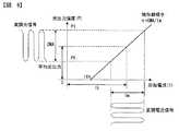
図6は、LDの印加電流と光出力強度の関係を示す。図6に示すように、LDに印加される直流電流(印加電流I)が、発振閾値Ithを超えるとLDが発光する。さらに、印加電流Iを大きくしていくと、光出力強度Pは印加電流Iに対して線形に増大する。この線形部分の傾きη(η=光出力強度P/印加電流I)をLDのスロープ効率という。図6に示すように、LDにバイアス電流Ibおよび変調電流Imを印加すると、変調された光出力が得られる。このIbおよびImの値は、所定の光出力とOMAまたは消光比が得られるように設定される。 FIG. 6 shows the relationship between the current applied to the LD and the light output intensity. As shown in FIG. 6, when the direct current (applied current I) applied to the LD exceeds the oscillation threshold value Ith, the LD emits light. Further, as the applied current I is increased, the light output intensity P increases linearly with respect to the applied current I. The slope η (η = light output intensity P / applied current I) of this linear portion is called LD slope efficiency. As shown in FIG. 6, when a bias current Ib and a modulation current Im are applied to the LD, a modulated light output is obtained. The values of Ib and Im are set so as to obtain a predetermined light output and OMA or extinction ratio.
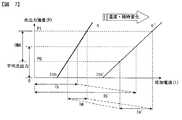
図7は、LDの温度変化および経時変化(印加電流と光出力強度の関係)を示す。図7のように、発振閾値Ithおよびスロープ効率ηは、温度変化および経時変化によって変化する。図7は、温度変化または経時変化によって、IthがIth′に増加すると共にηがη′に小さくなるように変化したとき、その変化に応じてバイアス電流IbをIb′に増大させると共に変調電流ImをIm′に増大させなければ、所定の光出力とOMAまたは消光比を得ることができないことを示している。 FIG. 7 shows changes in LD temperature and changes with time (relationship between applied current and light output intensity). As shown in FIG. 7, the oscillation threshold value Ith and the slope efficiency η change with temperature change and time change. FIG. 7 shows that when Ith increases to Ith ′ and η decreases to η ′ due to temperature change or change with time, the bias current Ib is increased to Ib ′ according to the change and the modulation current Im is increased. It is shown that a predetermined light output and OMA or extinction ratio cannot be obtained unless I is increased to Im ′.
LDの光出力強度の変化を避けるためのバイアス電流の制御には、光出力をモニタし、バイアス電流にフィードバックをかけるAPC(Automatic Power Control :自動光出力制御)が用いられる。OMAまたは消光比の変化を避けるための手段として、以下のものがある。 APC (Automatic Power Control) that monitors the optical output and applies feedback to the bias current is used to control the bias current to avoid the change in the optical output intensity of the LD. Means for avoiding changes in OMA or extinction ratio include the following.
(1)温度センサを使用してLDの周囲温度を測定し、その周囲温度に応じて変調電流を制御する構成(例えば、特許文献1参照。)。 (1) A configuration in which the ambient temperature of the LD is measured using a temperature sensor, and the modulation current is controlled according to the ambient temperature (see, for example, Patent Document 1).
(2)光出力をモニタするPD(フォトダイオード)の光電流から、ピークホールド回路等を用いてOMAまたは消光比を測定し、変調電流にフィードバックをかける構成(例えば、特許文献2参照。)。 (2) A configuration in which an OMA or extinction ratio is measured from a photocurrent of a PD (photodiode) that monitors optical output using a peak hold circuit or the like, and feedback is applied to the modulation current (see, for example, Patent Document 2).
(3)バイアス電流または変調電流に、低周波数のRF信号を重畳し、光出力をモニタするPDの光電流からRF信号成分のみを抽出し、OMAまたは消光比等を測定し、変調電流にフィードバックをかける構成(例えば、特許文献3参照。)。 (3) Superimpose a low-frequency RF signal on the bias current or modulation current, extract only the RF signal component from the PD photocurrent that monitors the optical output, measure the OMA or extinction ratio, and feed back to the modulation current (For example, refer to Patent Document 3).
(4)バイアス電流および変調電流の変動量から、OMAまたは消光比が一定になるようなバイアス電流または変調電流を予測し、変調電流にフィードフォワードをかける方法。この方法は、LD特性の変化によるバイアス電流および変調電流の変化は、その原因が温度変化または経時変化のどちらであっても、同じ変化をするという統計的予測に基づいており、具体的には、バイアス電流の変動量と変調電流の変動量との比が一定になるような制御を行い、製造時にその比を設定する。或いは、製造時に周囲温度を変化させて、OMAまたは消光比が一定になるようなバイアス電流および変調電流のデータを取り、そのデータに基づいて制御を行うものである。 (4) A method of predicting a bias current or a modulation current such that the OMA or the extinction ratio is constant from the fluctuation amount of the bias current and the modulation current, and applying the feed forward to the modulation current. This method is based on a statistical prediction that changes in bias current and modulation current due to changes in LD characteristics are the same regardless of whether the cause is a temperature change or a change over time. The control is performed so that the ratio between the fluctuation amount of the bias current and the fluctuation amount of the modulation current becomes constant, and the ratio is set at the time of manufacturing. Alternatively, the bias temperature and the modulation current data are taken so that the OMA or the extinction ratio becomes constant by changing the ambient temperature at the time of manufacture, and the control is performed based on the data.
前記(1)は、最も簡易に構成でき、広く利用されている方法である。また、前記(2)は、直接消光比を測定するため、確実に消光比を制御できる。更に、前記(3)は、PDの応答速度に対応できる低周波数のRF信号を用いるため、光出力のピーク値をとらえることができる。
しかし、従来のレーザダイオードの制御方法、制御回路、および光送信器によると、前記(1)は、LD特性の経時変化には対応できず、また、LDの温度特性の個体差が大きいため、製造時の調整が難しい。前記(2)は、伝送信号が高速になると、伝送速度が光出力をモニタするPDの応答速度よりも速すぎ、ピーク検出ができなくなる。また、外付けの回路が増えるため、光送信器を小型化することが難しくなる。 However, according to the conventional laser diode control method, control circuit, and optical transmitter, the above (1) cannot cope with changes in LD characteristics over time, and the individual differences in LD temperature characteristics are large. Adjustment during manufacturing is difficult. In (2), when the transmission signal becomes high speed, the transmission speed is too higher than the response speed of the PD that monitors the optical output, and peak detection cannot be performed. Further, since the number of external circuits increases, it is difficult to reduce the size of the optical transmitter.
前記(3)は、伝送信号に余分な試験信号を重畳するため、光波形の劣化やジッタの増大、発振などのリスクを伴う。また、外付けの回路が増えるため、高密度実装には不向きである。更に、前記(4)は、経時変化に対する保証が統計的なものにとどまるほか、LDの特性のばらつきのため、製造時の調整にかかる負荷が大きい。 The above (3) is accompanied by risks such as deterioration of the optical waveform, increase in jitter, and oscillation because an extra test signal is superimposed on the transmission signal. Further, since the number of external circuits increases, it is not suitable for high-density mounting. Further, in (4), the guarantee for the change with time is not limited to a statistical one, and because of the variation in the characteristics of the LD, the load for adjustment at the time of manufacture is large.
したがって、本発明の目的は、製造時の調整が容易に行え、光信号特性を劣化させず、かつ高密度実装を可能にする光送信器のレーザダイオードの制御方法、制御回路、および光送信器を提供することにある。 Accordingly, an object of the present invention is to provide a laser diode control method, a control circuit, and an optical transmitter that can be easily adjusted at the time of manufacture, do not deteriorate optical signal characteristics, and enable high-density mounting. Is to provide.
本発明は、前記の目的を達成するため、第1の特徴として、レーザダイオードにバイアス電流および変調電流を印加して前記レーザダイオードの光出力を変調すると共に、前記レーザダイオードの光出力と、光変調振幅または消光比とを制御するレーザダイオードの制御方法において、前記レーザダイオードの光出力を測定する第1の工程と、前記光出力が所定の値に一致するようにバイアス電流を調整するAPC(自動光出力制御)を行うと共に、スロープ効率または前記スロープ効率の相当量を測定する第2の工程と、前記光変調振幅または消光比が所定の値に一致するように前記スロープ効率またはその相当量に応じてAAC(自動光変調振幅制御)により前記変調電流を調整する第3の工程とを含むことを特徴とするレーザダイオードの制御方法を提供する。 In order to achieve the above object, the present invention provides, as a first feature, modulating a light output of the laser diode by applying a bias current and a modulation current to the laser diode, In a laser diode control method for controlling a modulation amplitude or an extinction ratio, a first step of measuring a light output of the laser diode, and an APC (adjusting a bias current so that the light output matches a predetermined value) A second step of measuring the slope efficiency or a corresponding amount of the slope efficiency, and the slope efficiency or the equivalent amount so that the light modulation amplitude or the extinction ratio matches a predetermined value. And a third step of adjusting the modulation current by AAC (automatic light modulation amplitude control) according to To provide a control method.
本発明は、前記の目的を達成するため、第2の特徴として、レーザダイオードにバイアス電流および変調電流を印加して前記レーザダイオードの出力を変調するレーザダイオードの制御回路において、受光素子により測定された前記レーザダイオードの光出力が所定の値に一致するようにバイアス電流を調整するAPC(自動光出力制御)部と、前記レーザダイオードのスロープ効率またはその相当量を測定するスロープ効率測定部と、前記光変調振幅または消光比が所定の値に一致するように変調電流を前記スロープ効率測定部による測定結果に応じて調整するAAC(自動光変調振幅制御)部とを備えることを特徴とするレーザダイオードの制御回路を提供する。 In order to achieve the above-mentioned object, the present invention has a second feature that is measured by a light receiving element in a laser diode control circuit that modulates the output of the laser diode by applying a bias current and a modulation current to the laser diode. An APC (automatic light output control) unit that adjusts a bias current so that a light output of the laser diode matches a predetermined value, a slope efficiency measurement unit that measures a slope efficiency of the laser diode or an equivalent amount thereof, A laser comprising: an AAC (automatic light modulation amplitude control) unit that adjusts a modulation current in accordance with a measurement result by the slope efficiency measurement unit so that the light modulation amplitude or extinction ratio matches a predetermined value. A diode control circuit is provided.
本発明は、前記の目的を達成するため、第3の特徴として、レーザダイオードと、前記レーザダイオードにバイアス電流を付与する電流源と、前記レーザダイオードに変調電流を印加して前記レーザダイオードの出力を変調する変調回路と、前記レーザダイオードの光出力を測定する光出力測定回路と、前記光出力が所定の値に一致するように前記バイアス電流を調整するAPC(自動光出力制御)、およびレーザダイオードのスロープ効率またはその相当量の測定結果に基づいて、前記光変調振幅または消光比が所定の値に一致するように、前記スロープ効率またはその相当量に応じて変調電流を調整するAAC(自動光変調振幅制御)を行う制御部とを備えることを特徴とする光送信器を提供する。 In order to achieve the above object, the present invention provides, as a third feature, a laser diode, a current source for applying a bias current to the laser diode, and a modulation current applied to the laser diode to output the laser diode. A modulation circuit that modulates the light, an optical output measurement circuit that measures the optical output of the laser diode, an APC (automatic optical output control) that adjusts the bias current so that the optical output matches a predetermined value, and a laser Based on the measurement result of the slope efficiency of the diode or its equivalent amount, an AAC (automatic adjustment) that adjusts the modulation current according to the slope efficiency or its equivalent amount so that the light modulation amplitude or extinction ratio matches a predetermined value. An optical transmitter comprising: a controller that performs (optical modulation amplitude control).
本発明のレーザダイオードの制御方法によれば、光出力の測定結果をフィードバックしてレーザダイオードのバイアス電流を制御すると共に、スロープ効率またはその相当量に基づいて変調電流を調整するようにしたので、製造時の調整が容易に行え、光信号特性の劣化を防止することができる。 According to the laser diode control method of the present invention, the measurement result of the optical output is fed back to control the bias current of the laser diode, and the modulation current is adjusted based on the slope efficiency or its equivalent amount. Adjustment at the time of manufacture can be easily performed and deterioration of optical signal characteristics can be prevented.
また、本発明のレーザダイオードの制御回路および光送信器によれば、光出力の測定結果をフィードバックしてレーザダイオードのバイアス電流を制御すると共に、スロープ効率またはその相当量に基づいて変調電流を調整するようにしたので、製造時の調整が容易に行え、光信号特性が劣化するのを防止でき、しかも高密度実装が可能になる。 In addition, according to the laser diode control circuit and the optical transmitter of the present invention, the bias current of the laser diode is controlled by feeding back the measurement result of the optical output, and the modulation current is adjusted based on the slope efficiency or its equivalent amount. As a result, adjustment during manufacture can be easily performed, optical signal characteristics can be prevented from deteriorating, and high-density mounting can be achieved.
以下、本発明の実施の形態について図面を基に説明する。
[第1の実施の形態]
(光送信器の構成)
図1は、本発明の第1の実施の形態に係る光送信器の構成を示す。
光送信器100は、バイアス電流および変調電流に応じた強度で発光したレーザ光を光導波路等へ出射するLD(レーザダイオード)1と、LD1に印加する変調電流を生成する変調回路2と、変調回路2に電流を印加する電流源3と、LD1にバイアス電流を印加する電流源4と、LD1の後方出力と光結合され、LD1の光出力をモニタする受光素子としてのPD(フォトダイオード)5と、光出力測定回路6と、周囲温度を測定する温度測定回路7と、プログラムを内蔵した制御部としてのマイクロプロセッサ8と、前記プログラムのほか、光出力およびOMAの目標値が格納されると共にマイクロプロセッサ8に接続された不揮発性メモリ9と、電流源3とマイクロプロセッサ8との間に接続されたD/A変換器10と、電流源4とマイクロプロセッサ8との間に接続されたD/A変換器11と、光出力測定回路6とマイクロプロセッサ8との間に接続されたA/D変換器12と、温度測定回路7とマイクロプロセッサ8との間に接続されたA/D変換器13と、トランジスタ2bのコレクタとLD1との間に接続されたコンデンサ14とを備える。Hereinafter, embodiments of the present invention will be described with reference to the drawings.
[First Embodiment]
(Configuration of optical transmitter)
FIG. 1 shows a configuration of an optical transmitter according to a first embodiment of the present invention.
The optical transmitter 100 includes an LD (laser diode) 1 that emits laser light emitted at an intensity corresponding to a bias current and a modulation current to an optical waveguide, a
LD1は、コンデンサ14により変調回路2に交流結合され、変調回路2による変調電流がLD1に印加される。このコンデンサ14からの変調電流が図6に示した変調電流Imになり、LD1からは変調された光出力が発生し、光導波路等に入射される。 LD1 is AC-coupled to the
LD1による光出力の論理“1”レベルをP1、“0”レベルをP0とすると、LD1の光出力の平均値はP1とP0の和の1/2であり、OMAおよび消光比はそれぞれ、P1とP0の差および比である。したがって、光出力の平均値とOMAが与えられれば、消光比は一意に決まるため、光出力とOMAを制御することで消光比も制御することができる。 When the logical “1” level of the optical output by LD1 is P1, and the “0” level is P0, the average value of the optical output of LD1 is ½ of the sum of P1 and P0, and the OMA and extinction ratio are P1 and P1, respectively. And the ratio and ratio of P0. Therefore, if the average value of the optical output and the OMA are given, the extinction ratio is uniquely determined. Therefore, the extinction ratio can also be controlled by controlling the optical output and the OMA.
変調回路2は、一対のトランジスタ2a,2bと、それぞれのコレクタと電源Vsの間に接続された抵抗2c,2dと、入力端子2e,2fとを備え、外部から入力端子2e,2fに与えられた送信信号S1,S2に基づいてトランジスタ2a,2bがスイッチングされることにより、LD1に印加する変調電流がトランジスタ2bのコレクタから出力される。 The
光出力測定回路6は、PD5に直列接続されたコンデンサ6aと、このコンデンサ6aに並列接続された抵抗6bとを備え、PD5の光電流出力を積分してLD1の光出力の平均値を生成し、その結果をA/D変換器12に印加する。 The optical output measurement circuit 6 includes a capacitor 6a connected in series to the PD 5 and a resistor 6b connected in parallel to the capacitor 6a, and integrates the photocurrent output of the PD 5 to generate an average value of the optical output of the
温度測定回路7は、電源Vsに接続された電流源7aと、この電流源7aに直列接続されたサーミスタ7bとを備える。サーミスタ7bは、設置雰囲気の温度に応じて抵抗値が変化し、その抵抗値に応じた端子電圧を温度検出値として生成する。 The
マイクロプロセッサ8は、例えば、CPUを用いて構成されると共に、光出力測定回路6および温度測定回路7によって測定された値に基づいて、電流源3,4の制御、変調電流およびバイアス電流の制御を、不揮発性メモリ9に格納されたプログラムに従って実行する。 The microprocessor 8 is configured using, for example, a CPU, and controls the current sources 3 and 4 and controls the modulation current and the bias current based on values measured by the light output measurement circuit 6 and the
この第1の実施の形態の動作は、次に説明する第2の実施の形態と同じであるので、図2を参照して第2の実施の形態と共に説明する。 Since the operation of the first embodiment is the same as that of the second embodiment described below, the operation will be described together with the second embodiment with reference to FIG.
[第2の実施の形態]
(レーザダイオードの制御方法)
図2は、本発明の第2の実施の形態に係るレーザダイオードの制御方法、および第1の実施の形態の光送信器の動作を示し、その実行はマイクロブロセッサ8によってなされる。なお、同図中、Sはステップを表している。[Second Embodiment]
(Control method of laser diode)
FIG. 2 shows the laser diode control method according to the second embodiment of the present invention and the operation of the optical transmitter according to the first embodiment, which is executed by the microprocessor 8. In the figure, S represents a step.
また、図3は、光出力およびバイアス電流の変動量とスロープ効率との関係を示す特性図である。図1〜図3を参照してレーザダイオードの制御方法およびマイクロプロセッサの動作を説明する。 FIG. 3 is a characteristic diagram showing the relationship between the fluctuation amount of the optical output and bias current and the slope efficiency. The laser diode control method and the microprocessor operation will be described with reference to FIGS.
本実施の形態においては、発振閾値Ithおよびスロープ効率ηの温度変化および経時変化に応じて、光出力およびOMA(光変調振幅)の自動制御が行われる。まず、マイクロプロセッサ8は、バイアス電流Ibおよび変調電流Imの各初期値を出力し、電流源3,4を制御する(S201)。これらの初期値は、LD1が過度の強度で発光し、対向の光受信機の受光素子が破壊するのを防止するため、なるべく小さな値にする。具体的には、光送信器100の動作温度範囲の最低温度におけるときの電流の半分程度の値でよい。LD1の個体差により、これらの値は異なるが、個別に調整する必要はなく、LD1のデータシート、設計値等から最も小さい駆動条件を算出すればよい。なお、これらの初期値は、予め不揮発性メモリ9に書き込まれている。 In the present embodiment, automatic control of the light output and OMA (light modulation amplitude) is performed in accordance with the temperature change and temporal change of the oscillation threshold value Ith and the slope efficiency η. First, the microprocessor 8 outputs initial values of the bias current Ib and the modulation current Im, and controls the current sources 3 and 4 (S201). These initial values are set as small as possible in order to prevent the
一方、光出力測定回路6によって光出力が測定され(第1の工程)、その測定値はA/D変換器12によってデジタル値に変換され、マイクロプロセッサ8に取り込まれる。マイクロプロセッサ8は、前記初期値とA/D変換器12の出力とに基づいて、光出力の平均値が予め設定された目標値に一致するように、その測定値をフィードバックし、バイアス電流を制御するAPC(自動光出力制御)を実行する(S202;第2の工程)。なお、光出力の目標値は、予め不揮発性メモリ9に書き込まれている。 On the other hand, the light output is measured by the light output measuring circuit 6 (first step), and the measured value is converted into a digital value by the A / D converter 12 and taken into the microprocessor 8. Based on the initial value and the output of the A / D converter 12, the microprocessor 8 feeds back the measured value so that the average value of the optical output matches a preset target value, and calculates the bias current. APC (automatic light output control) to be controlled is executed (S202; second step). The target value of light output is written in the
このAPCの実行過程において、マイクロプロセッサ8は、光出力測定回路6による光出力強度Pと印加電流Iとから、LD1のスロープ効率ηを測定する(S202;第2の工程)。この工程で、APCの実行過程における光出力の測定値の変動量ΔPとバイアス電流の変動量ΔIbが得られる。図3に示すように、LD1のIthおよびηが破線で示す特性から、実線で示す特性に変化し、APCを行う前に光出力がΔPだけ減少すると、光出力を目標値に一致させるために、APCによってバイアス電流はΔIbの増加がなされる。このとき、ΔPとΔIbの比、ΔP/ΔIbがスロープ効率ηになるので、容易にηを算出することができる。 In this APC execution process, the microprocessor 8 measures the slope efficiency η of the
次に、マイクロプロセッサ8は、S202で得られたスロープ効率ηに基づいてAAC(自動光変調振幅制御)を実行する(S204;第3の工程)。このAACは、予め設定されたOMAの目標値と一致するように、変調電流Imをηに基づいて算出することにより行われる。具体的には、OMAとImの比がηであるから、OMAが一定のとき、Imはηに反比例する。したがって、OMAの目標値とηの比はImになる。なお、OMAの目標値は、不揮発性メモリ9に予め書き込まれている。 Next, the microprocessor 8 executes AAC (automatic light modulation amplitude control) based on the slope efficiency η obtained in S202 (S204; third step). This AAC is performed by calculating the modulation current Im based on η so as to coincide with a preset OMA target value. Specifically, since the ratio of OMA to Im is η, when OMA is constant, Im is inversely proportional to η. Therefore, the ratio between the target value of OMA and η is Im. The OMA target value is written in the
次に、マイクロプロセッサ8は、光出力測定回路6によって測定された光出力の測定値をチェックする(S205)。LD1の特性が、温度変化または経時変化によって変化し、その測定値が光出力の目標値と一致しない場合、処理をS202に戻し、光出力の測定値が目標値と一致するまで、APCおよびAACを繰り返し実行する。これにより、温度変化および経時変化に応じたLD制御を行うことができる。光出力=目標値であれば、S204の結果を維持する。 Next, the microprocessor 8 checks the measurement value of the light output measured by the light output measurement circuit 6 (S205). If the characteristics of the LD1 change due to a temperature change or a change over time and the measured value does not match the target value of the light output, the process returns to S202, and APC and AAC are performed until the measured value of the light output matches the target value. Repeatedly. Thereby, LD control according to a temperature change and a time-dependent change can be performed. If light output = target value, the result of S204 is maintained.
(光出力およびOMAの目標値の決定方法)
次に、前記光出力およびOMAの目標値の決定方法について説明する。LD1の後方出力とPD5の光結合効率は、一般的に、組み立ての際にばらつきが生じる。そのため、光出力およびOMAの目標値を個別に調整する必要がある。しかし、組立工程において、LD1の前方出力と光導波路とを光結合させるために調芯する際、PD5の光電流も同時に測定することができるため、LD1の前方出力とPD5の光電流の比を予め知ることができる。この比を用いて光出力およびOMAの目標値を算出すればよい。(Method for determining optical output and OMA target values)
Next, a method for determining the optical output and the OMA target value will be described. Generally, the rear output of the
LD1の前方出力とPD5の光結合効率が、温度によって変動することがしばしば発生する。光結合効率の変動量は、一般に、25〜70℃において±0.5dB程度である。高い精度で制御したい場合は、恒温槽などを用い、必要な温度範囲において周囲温度をスイープさせ、LD1の前方出力とPD5の光電流との比の温度特性データを測定する。それらのデータから、各温度における光出力およびOMAの目標値を算出し、目標値のテーブルをそれぞれ作成し、不揮発性メモリ9に記憶する。このとき、S202およびS204における処理は、温度測定回路7で測定された温度を読み込み、テーブルからその温度に対応する目標値を取得する。 It often happens that the forward output of LD1 and the optical coupling efficiency of PD5 vary with temperature. The fluctuation amount of the optical coupling efficiency is generally about ± 0.5 dB at 25 to 70 ° C. When it is desired to control with high accuracy, a constant temperature bath or the like is used, the ambient temperature is swept in a necessary temperature range, and the temperature characteristic data of the ratio between the front output of LD1 and the photocurrent of PD5 is measured. From these data, the light output at each temperature and the target value of OMA are calculated, and a table of target values is created and stored in the
(第1および第2の実施の形態の効果)
この第1および第2の実施の形態によれば、APCによりバイアス電流を調整すると共に、スロープ効率ηまたはその相当量に基づいてAACによりOMAまたは消光比を所定の値になるようにすることにより、LD1の温度特性の個体差によらず製造時の調整が容易に行え、光信号特性の劣化を防止することができる。(Effects of the first and second embodiments)
According to the first and second embodiments, the bias current is adjusted by APC, and the OMA or extinction ratio is set to a predetermined value by AAC based on the slope efficiency η or its equivalent amount. Therefore, adjustment during manufacture can be easily performed regardless of individual differences in temperature characteristics of the LD1, and deterioration of optical signal characteristics can be prevented.
更に、発振閾値Ithおよびスロープ効率の温度変化および経時変化に応じて、光出力およびOMAの自動制御を行うようにしたので、LD特性の経時変化に対応することが可能になる。 Furthermore, since the optical output and the OMA are automatically controlled according to the temperature change and the time change of the oscillation threshold value Ith and the slope efficiency, it becomes possible to cope with the time change of the LD characteristics.
[第3の実施の形態]
(レーザダイオードの制御方法)
図4は、本発明の第3の実施の形態に係るレーザダイオードの制御方法を示す。同図中、Sはステップを表している。本実施の形態は、第2の実施の形態におけるS201およびS202の処理が異なる他は、第2の実施の形態と同じである。図4における処理も不揮発性メモリ9に格納されたプログラムに従ってマイクロプロセッサ8が実行する。[Third Embodiment]
(Control method of laser diode)
FIG. 4 shows a laser diode control method according to the third embodiment of the present invention. In the figure, S represents a step. The present embodiment is the same as the second embodiment except that the processes of S201 and S202 in the second embodiment are different. The processing in FIG. 4 is also executed by the microprocessor 8 according to the program stored in the
マイクロプロセッサ8は、S201の処理を実行後、APCを行うと共に、光出力の変動に伴って変化したバイアス電流の変動量ΔIbをηの相当量としてΔIb測定をする(S202)。次に、ΔP(光出力の変動量)=ΔPs(設定値)か否かを判定する(S301)。光出力測定回路6で測定されたΔPが予め決められたΔPsになったとき、マイクロプロセッサ8の処理はS204へ移行する。S204の処理においては、測定されたΔIbに比例した変調電流Imを出力する。その後、光出力が目標値になるまで、以上のシーケンスが繰り返し実行される。なお、ImとΔIbの比例定数は、目標とするOMAとΔPsの比、OMA/ΔPs=Im/ΔIbであり、予め不揮発性メモリ9に格納されている。 The microprocessor 8 performs APC after executing the process of S201, and performs ΔIb measurement with the variation amount ΔIb of the bias current changed with the variation of the optical output as the equivalent amount of η (S202). Next, it is determined whether or not ΔP (light output fluctuation amount) = ΔPs (set value) (S301). When ΔP measured by the light output measurement circuit 6 becomes ΔPs determined in advance, the processing of the microprocessor 8 proceeds to S204. In the process of S204, a modulation current Im proportional to the measured ΔIb is output. Thereafter, the above sequence is repeatedly executed until the light output reaches the target value. The proportional constant between Im and ΔIb is a target ratio of OMA and ΔPs, OMA / ΔPs = Im / ΔIb, and is stored in the
さらに、マイクロプロセッサ8は、光出力測定回路6によって測定された光出力の測定値を監視し続け(S205)、LD1の特性が、温度変化または経時変化によって変化し、その測定値が光出力の目標値と一致しない場合は処理をS202に戻し、光出力の測定値が目標値と一致するまで、APCおよびAACを繰り返し実行する。これにより、温度変化および経時変化に応じたLD制御を行うことができる。光出力=目標値であれば、S204の結果を維持する。 Further, the microprocessor 8 continues to monitor the measurement value of the light output measured by the light output measurement circuit 6 (S205), and the characteristics of the LD1 change due to the temperature change or the change over time, and the measurement value becomes the light output value. If it does not match the target value, the process returns to S202, and APC and AAC are repeatedly executed until the measured value of the optical output matches the target value. Thereby, LD control according to a temperature change and a time-dependent change can be performed. If light output = target value, the result of S204 is maintained.
(第3の実施の形態の効果)
この第3の実施の形態によれば、前記した第1および第2の実施の形態と同様の効果が得られるほか、マイクロプロセッサ8の処理にかかる時間を軽減することができる。(Effect of the third embodiment)
According to the third embodiment, the same effects as those of the first and second embodiments described above can be obtained, and the time required for processing by the microprocessor 8 can be reduced.
[第4の実施の形態]
(制御回路の構成)
図5は、本発明の第4の実施の形態に係るレーザダイオードの制御回路を示す。本実施の形態は、図1の第1の実施の形態において、マイクロプロセッサ8に代えて、スロープ効率測定部15と、APC(自動光出力制御)部16と、AAC(自動光変調振幅制御)部17と、これらのほか不揮発性メモリ9および温度測定回路7に接続されて全体を管理する制御部18とを設け、制御回路500を構成したものである。他の構成は、図1の第1の実施の形態と同様である。従って、図5においては、図1に示したと同一であるものには同一引用数字を用いると共に、重複する説明は省略する。[Fourth Embodiment]
(Configuration of control circuit)
FIG. 5 shows a laser diode control circuit according to the fourth embodiment of the present invention. In the present embodiment, in place of the microprocessor 8 in the first embodiment of FIG. 1, a slope
スロープ効率測定部15は、LD1のスロープ効率またはその相当量を測定し、制御部18へ出力する。APC部16は、光出力測定回路6による光出力を所定の値に一致するようにバイアス電流を調整する。AAC部17は、光変調振幅または消光比が所定の値に一致するように変調電流をスロープ効率測定部15による測定結果に応じて調整する。なお、これらの機能をマイクロプロセッサ8に持たせる構成にすることも可能である。その場合の構成は、図1と同じになる。 The slope
(第4の実施の形態の動作)
第4の実施の形態による制御は、図2および図4で説明した通りである。図2の制御による場合、S202の処理がAPC部16によって行われ、S203の処理がスロープ効率測定部15によって行われ、その測定結果は制御部18を介して不揮発性メモリ9に記憶され、必要時に読み出されてAAC部17に供与される。また、S204の処理がAAC部17によって行われる。その他の制御は、制御部18によって実行される。また、図4の制御による場合、S301、S302の処理がスロープ効率測定部15によって行われる。他は、図2の制御と同じである。(Operation of the fourth embodiment)
The control according to the fourth embodiment is as described with reference to FIGS. In the case of the control of FIG. 2, the process of S202 is performed by the
(第4の実施の形態の効果)
この第4の実施の形態によれば、第1の実施の形態と同様に、APC部16によりバイアス電流を調整し、スロープ効率またはその相当量に基づいてAAC部17により光変調振幅間または消光比を所定の値になるようにすることにより、LD1の温度特性の個体差によらず製造時の調整が容易に行え、光信号特性の劣化を防止することができる。(Effect of the fourth embodiment)
According to the fourth embodiment, as in the first embodiment, the
更に、発振閾値Ithおよびスロープ効率の温度変化および経時変化に応じて、光出力およびOMAの自動制御を行うようにしたので、LD特性の経時変化に対応することが可能になる。 Furthermore, since the optical output and the OMA are automatically controlled according to the temperature change and the time change of the oscillation threshold value Ith and the slope efficiency, it becomes possible to cope with the time change of the LD characteristics.
[他の実施の形態]
前記実施の形態においては、LD1と変調回路2のトランジスタ2bとをコンデンサ14による交流結合にしたが、両方のトランジスタと交流結合する差動駆動方式としてもよい。また、LD1と変調回路2との結合は、交流結合に代えて直流結合とすることも可能である。[Other embodiments]
In the above embodiment, the
また、第1の実施の形態においては、マイクロプロセッサ8を用いてLD1のAPCおよびAACを行ったが、これに限るものではない。例えば、論理回路、アナログ演算回路、および各種の半導体素子を用いて構成してもよい。 In the first embodiment, the APC and AAC of the
また、第2の実施の形態においては、S204のAACを行うに際しては、変調電流Imの変動が大きい場合、チャープの増大を防ぐために、例えば、計算で得られた変調電流Imの1/10ずつの変化としてもよい。 In the second embodiment, when the AAC of S204 is performed, if the variation in the modulation current Im is large, in order to prevent an increase in chirp, for example, 1/10 each of the modulation current Im obtained by calculation It may be a change.
更に、前記各実施の形態においては、光出力およびOMA(光変調振幅)を一定にする制御を行ったが、或る状態に応じて光出力またはOMAの目標値を変化させる制御を行っても良い。例えば、温度や信号の伝送速度の状態、あるいは温度やバイアス電流、変調電流が所定の閾値を超えた状態、信号無入力状態等に応じて、目標値を変化させることができる。 Further, in each of the above embodiments, the control for making the optical output and OMA (optical modulation amplitude) constant is performed, but the control for changing the optical output or the target value of OMA according to a certain state may be performed. good. For example, the target value can be changed in accordance with the state of the temperature or the transmission speed of the signal, the state where the temperature, the bias current, the modulation current exceeds a predetermined threshold, the signal non-input state, or the like.
1 LD(レーザダイオード)
2 変調回路
2a,2b トランジスタ
2c,2d 抵抗
2e,2f 入力端子
3,4 電流源
5 PD(フォトダイオード)
6 光出力測定回路
6a コンデンサ
6b 抵抗
7 温度測定回路
7a 電流源
7b サーミスタ
8 マイクロプロセッサ
9 不揮発性メモリ
10,11 D/A変換器
12,13 A/D変換器
14 コンデンサ
15 スロープ効率測定部
16 APC部
17 AAC部
18 制御部
100 光送信器
500 制御回路1 LD (laser diode)
2
6 Optical Output Measurement Circuit 6a
Claims (15)
Translated fromJapanese前記レーザダイオードの光出力を測定する第1の工程と、
前記光出力が所定の値に一致するようにバイアス電流を調整するAPC(自動光出力制御)を行うと共に、スロープ効率または前記スロープ効率の相当量を測定する第2の工程と、
前記光変調振幅または消光比が所定の値に一致するように前記スロープ効率またはその相当量に応じてAAC(自動光変調振幅制御)により前記変調電流を調整する第3の工程とを含むことを特徴とするレーザダイオードの制御方法。In a laser diode control method for applying a bias current and a modulation current to a laser diode to modulate the light output of the laser diode, and controlling the light output of the laser diode and the light modulation amplitude or extinction ratio,
A first step of measuring the light output of the laser diode;
A second step of performing APC (automatic light output control) for adjusting a bias current so that the light output matches a predetermined value, and measuring a slope efficiency or a substantial amount of the slope efficiency;
And a third step of adjusting the modulation current by AAC (automatic light modulation amplitude control) in accordance with the slope efficiency or an equivalent amount thereof so that the light modulation amplitude or extinction ratio matches a predetermined value. A method for controlling a laser diode.
前記第3の工程は、前記受光素子の光電流および前記レーザダイオードの設置雰囲気の温度検出値に基づいて、前記光出力の所定の値および前記光変調振幅の所定の値を変化させることを特徴とする請求項1記載のレーザダイオードの制御方法。In the first step, the light output of the laser diode is measured by a light receiving element,
In the third step, the predetermined value of the light output and the predetermined value of the light modulation amplitude are changed based on a photocurrent of the light receiving element and a temperature detection value of an installation atmosphere of the laser diode. The laser diode control method according to claim 1.
受光素子により測定された前記レーザダイオードの光出力が所定の値に一致するようにバイアス電流を調整するAPC(自動光出力制御)部と、
前記レーザダイオードのスロープ効率またはその相当量を測定するスロープ効率測定部と、
前記光変調振幅または消光比が所定の値に一致するように変調電流を前記スロープ効率測定部による測定結果に応じて調整するAAC(自動光変調振幅制御)部とを備えることを特徴とするレーザダイオードの制御回路。In a laser diode control circuit that modulates the output of the laser diode by applying a bias current and a modulation current to the laser diode,
An APC (automatic light output control) unit that adjusts the bias current so that the light output of the laser diode measured by the light receiving element matches a predetermined value;
A slope efficiency measuring unit for measuring the slope efficiency of the laser diode or an equivalent amount thereof;
A laser comprising: an AAC (automatic light modulation amplitude control) unit that adjusts a modulation current in accordance with a measurement result by the slope efficiency measurement unit so that the light modulation amplitude or extinction ratio matches a predetermined value. Diode control circuit.
前記AAC部は、前記相当量に比例した変調電流を出力することを特徴とする請求項6記載のレーザダイオードの制御回路。The slope efficiency measurement unit, when the fluctuation amount of the optical output in the process of the APC reaches a predetermined value, the fluctuation amount of the bias current is regarded as a substantial amount of the slope efficiency,
The laser diode control circuit according to claim 6, wherein the AAC unit outputs a modulation current proportional to the equivalent amount.
前記レーザダイオードにバイアス電流を付与する電流源と、
前記レーザダイオードに変調電流を印加して前記レーザダイオードの出力を変調する変調回路と、
前記レーザダイオードの光出力を測定する光出力測定回路と、
前記光出力が所定の値に一致するように前記バイアス電流を調整するAPC(自動光出力制御)、およびレーザダイオードのスロープ効率またはその相当量の測定結果に基づいて、前記光変調振幅または消光比が所定の値に一致するように、前記スロープ効率またはその相当量に応じて変調電流を調整するAAC(自動光変調振幅制御)を行う制御部とを備えることを特徴とする光送信器。A laser diode;
A current source for applying a bias current to the laser diode;
A modulation circuit for modulating the output of the laser diode by applying a modulation current to the laser diode;
A light output measuring circuit for measuring a light output of the laser diode;
Based on APC (automatic light output control) for adjusting the bias current so that the light output matches a predetermined value, and the measurement result of the slope efficiency of the laser diode or its equivalent amount, the light modulation amplitude or the extinction ratio An optical transmitter comprising: a control unit that performs AAC (automatic optical modulation amplitude control) that adjusts a modulation current according to the slope efficiency or an equivalent amount thereof so that the value coincides with a predetermined value.
前記制御部は、前記受光素子の光電流および前記レーザダイオードの設置雰囲気の温度検出値に基づいて、前記光出力の所定の値および前記光変調振幅の所定の値を変化させることを特徴とする請求項11,12または13記載の光送信器。A light receiving element for measuring the light output of the laser diode;
The control unit changes a predetermined value of the light output and a predetermined value of the light modulation amplitude based on a photocurrent of the light receiving element and a temperature detection value of an installation atmosphere of the laser diode. The optical transmitter according to claim 11, 12 or 13.
Priority Applications (2)
| Application Number | Priority Date | Filing Date | Title |
|---|---|---|---|
| JP2004190371AJP2006013252A (en) | 2004-06-28 | 2004-06-28 | Laser diode control method, control circuit, and optical transmitter |
| US11/042,329US7483455B2 (en) | 2004-06-28 | 2005-01-26 | Control method and control circuit for laser diode, and optical transmitter using the same |
Applications Claiming Priority (1)
| Application Number | Priority Date | Filing Date | Title |
|---|---|---|---|
| JP2004190371AJP2006013252A (en) | 2004-06-28 | 2004-06-28 | Laser diode control method, control circuit, and optical transmitter |
Publications (1)
| Publication Number | Publication Date |
|---|---|
| JP2006013252Atrue JP2006013252A (en) | 2006-01-12 |
Family
ID=35505671
Family Applications (1)
| Application Number | Title | Priority Date | Filing Date |
|---|---|---|---|
| JP2004190371APendingJP2006013252A (en) | 2004-06-28 | 2004-06-28 | Laser diode control method, control circuit, and optical transmitter |
Country Status (2)
| Country | Link |
|---|---|
| US (1) | US7483455B2 (en) |
| JP (1) | JP2006013252A (en) |
Cited By (4)
| Publication number | Priority date | Publication date | Assignee | Title |
|---|---|---|---|---|
| JP2007201043A (en)* | 2006-01-25 | 2007-08-09 | Opnext Japan Inc | Optical transmitter and optical transceiver |
| JP2009004525A (en)* | 2007-06-21 | 2009-01-08 | Fujitsu Ltd | Light source module |
| JP2010093123A (en)* | 2008-10-09 | 2010-04-22 | Opnext Japan Inc | Optical transmission apparatus and control method of optical transmission signal |
| JP2014064014A (en)* | 2013-11-05 | 2014-04-10 | Japan Oclaro Inc | Optical transmission apparatus and control method of optical transmission signal |
Families Citing this family (17)
| Publication number | Priority date | Publication date | Assignee | Title |
|---|---|---|---|---|
| EP2305812A3 (en)* | 2002-11-14 | 2012-06-06 | Dharmacon, Inc. | Fuctional and hyperfunctional sirna |
| KR100819308B1 (en)* | 2005-09-02 | 2008-04-03 | 삼성전자주식회사 | ROPE link device to enable stable TD system wireless service |
| US7349454B2 (en)* | 2005-09-09 | 2008-03-25 | Avago Technologies Fiber Ip Pte Ltd | Method of monitoring and controlling a laser diode |
| GB2432037B (en)* | 2005-11-01 | 2011-04-20 | Agilent Technologies Inc | A method and system for stabilizing operation of laser sources |
| US7817881B2 (en)* | 2006-06-01 | 2010-10-19 | Bing Li | Circuit architecture for electro-optic modulation based on free carrier dispersion effect and the waveguide capacitor structures for such modulator circuitry using CMOS or Bi-CMOS process |
| JP2008053536A (en)* | 2006-08-25 | 2008-03-06 | Sumitomo Electric Ind Ltd | Laser diode control device and laser diode control method |
| JP4341708B2 (en)* | 2007-08-13 | 2009-10-07 | オムロン株式会社 | Semiconductor laser driving device, semiconductor laser driving method, optical transmission device, optical wiring module, and electronic apparatus |
| JP5749458B2 (en)* | 2010-07-21 | 2015-07-15 | 富士通オプティカルコンポーネンツ株式会社 | Optical transmission module and method for controlling optical transmission module |
| US9178085B2 (en) | 2010-12-22 | 2015-11-03 | Bing Li | Waveguide photodetector and forming method thereof |
| US8983241B2 (en) | 2010-12-22 | 2015-03-17 | Bing Li | Optical waveguide switch |
| CN102565932B (en) | 2011-01-14 | 2014-10-08 | 李冰 | Dispersion-corrected arrayed waveguide grating |
| CN104349436B (en)* | 2013-08-07 | 2017-12-19 | 联芯科技有限公司 | The automatic obtaining method and device of automated power control code word |
| WO2015044942A2 (en)* | 2013-09-30 | 2015-04-02 | Corning Optical Communications Wireless Ltd. | Determining efficiency of an optical signal source in distributed communication systems |
| US9438005B1 (en)* | 2014-06-02 | 2016-09-06 | Google Inc. | Calibration of a tunable DBR laser |
| JP6720527B2 (en)* | 2015-12-25 | 2020-07-08 | 富士通株式会社 | Amplifying circuit, optical module and amplifying method |
| CN111600193B (en)* | 2020-05-28 | 2021-12-14 | 成都优博创通信技术有限公司 | Optical module debugging method and device, electronic equipment and storage medium |
| CN117233457B (en)* | 2023-11-16 | 2024-03-12 | 成都明夷电子科技有限公司 | Method and equipment for testing high-speed modulation current of laser |
Family Cites Families (13)
| Publication number | Priority date | Publication date | Assignee | Title |
|---|---|---|---|---|
| US4592057A (en)* | 1981-03-23 | 1986-05-27 | International Business Machines Corporation | Versatile digital controller for light emitting semiconductor devices |
| GB2260667B (en)* | 1991-10-19 | 1995-10-25 | Northern Telecom Ltd | Optical transmitters |
| US5812572A (en)* | 1996-07-01 | 1998-09-22 | Pacific Fiberoptics, Inc. | Intelligent fiberoptic transmitters and methods of operating and manufacturing the same |
| US6055252A (en)* | 1998-09-10 | 2000-04-25 | Photonic Solutions, Inc. | Fiberoptic transmitter using thermistor to maintain stable operating conditions over a range of temperature |
| US6845118B1 (en)* | 1999-01-25 | 2005-01-18 | Optical Communication Products, Inc. | Encapsulated optoelectronic devices with controlled properties |
| US6414974B1 (en)* | 1999-09-07 | 2002-07-02 | Analog Devices, Inc. | Method and a control circuit for controlling the extinction ratio of a laser diode |
| US6711189B1 (en)* | 2000-02-04 | 2004-03-23 | Stratos Lightwave, Inc. | Automatic power control and laser slope efficiency normalizing circuit |
| US6671248B2 (en)* | 2000-05-18 | 2003-12-30 | Matsushita Electric Industrial Co., Ltd. | Apparatus and method of controlling laser power |
| JP2001352125A (en) | 2000-06-07 | 2001-12-21 | Matsushita Electric Ind Co Ltd | APC type laser diode drive circuit |
| JP2002111120A (en) | 2000-09-28 | 2002-04-12 | Toshiba Electronic Engineering Corp | Optical transmission module |
| US6661817B1 (en)* | 2001-09-18 | 2003-12-09 | International Business Machines Corporation | Laser diode monitoring via current mirroring |
| JP3662534B2 (en) | 2001-11-30 | 2005-06-22 | 松下電器産業株式会社 | Optical transmitter |
| US7433375B2 (en)* | 2003-10-09 | 2008-10-07 | National Semiconductor Corporation | Laser trim and compensation methodology for passively aligning optical transmitter |
- 2004
- 2004-06-28JPJP2004190371Apatent/JP2006013252A/enactivePending
- 2005
- 2005-01-26USUS11/042,329patent/US7483455B2/ennot_activeExpired - Fee Related
Cited By (4)
| Publication number | Priority date | Publication date | Assignee | Title |
|---|---|---|---|---|
| JP2007201043A (en)* | 2006-01-25 | 2007-08-09 | Opnext Japan Inc | Optical transmitter and optical transceiver |
| JP2009004525A (en)* | 2007-06-21 | 2009-01-08 | Fujitsu Ltd | Light source module |
| JP2010093123A (en)* | 2008-10-09 | 2010-04-22 | Opnext Japan Inc | Optical transmission apparatus and control method of optical transmission signal |
| JP2014064014A (en)* | 2013-11-05 | 2014-04-10 | Japan Oclaro Inc | Optical transmission apparatus and control method of optical transmission signal |
Also Published As
| Publication number | Publication date |
|---|---|
| US20050286575A1 (en) | 2005-12-29 |
| US7483455B2 (en) | 2009-01-27 |
Similar Documents
| Publication | Publication Date | Title |
|---|---|---|
| JP2006013252A (en) | Laser diode control method, control circuit, and optical transmitter | |
| US7061950B2 (en) | Drive circuit and drive method of semiconductor laser module provided with electro-absorption type optical modulator | |
| US6795458B2 (en) | Laser diode control circuit and laser diode control method | |
| EP0215311A2 (en) | Laser diode driving circuit | |
| US20060027736A1 (en) | Light-receiving circuit | |
| KR20100024517A (en) | Semiconductor laser drive apparatus, semiconductor laser drive method, optical transmitter, optical wiring module, and electronic device | |
| CN108390724A (en) | Transmitting optical power adjusting method, device and the optical module of optical module | |
| US6965357B2 (en) | Light-emitting element drive circuit | |
| US20020041728A1 (en) | Optical transmission system and terminal device applicable to the system | |
| US7236506B2 (en) | Method and apparatus for compensating for temperature characteristics of laser diode in optical communication system | |
| KR20200110986A (en) | Controller of optical transmitter | |
| CN110783815B (en) | Method for estimating a condition parameter, device for monitoring operation and particle sensor device | |
| JP2694803B2 (en) | Optical semiconductor laser device wavelength stabilization method | |
| JP2005057216A (en) | Laser diode drive circuit and optical transmitter | |
| JP2008078437A (en) | Semiconductor laser module | |
| US9325153B2 (en) | Method to control transmitter optical module | |
| JP2830794B2 (en) | Optical transmission circuit | |
| JP2019109342A (en) | Optical transmission subassembly and optical module | |
| JPH11238932A (en) | Semiconductor laser device and laser-light receiver | |
| TWI638496B (en) | DC-coupled optical communication module with extinction ratio compensation function and extinction ratio compensation method for high-speed optical communication module | |
| JP2005150620A (en) | Semiconductor laser device | |
| JPH0834328B2 (en) | LD emission wavelength controller | |
| US6441940B1 (en) | Wavelength stabilization of light emitting components | |
| JPH07162597A (en) | Device for making light quantity constant in image input device or the like | |
| JPS61224385A (en) | Semiconductor laser drive circuit |