JP2006004076A - Semiconductor integrated device design method, design program, and recording medium - Google Patents
Semiconductor integrated device design method, design program, and recording mediumDownload PDFInfo
- Publication number
- JP2006004076A JP2006004076AJP2004178372AJP2004178372AJP2006004076AJP 2006004076 AJP2006004076 AJP 2006004076AJP 2004178372 AJP2004178372 AJP 2004178372AJP 2004178372 AJP2004178372 AJP 2004178372AJP 2006004076 AJP2006004076 AJP 2006004076A
- Authority
- JP
- Japan
- Prior art keywords
- bus
- transaction data
- semiconductor integrated
- control unit
- integrated device
- Prior art date
- Legal status (The legal status is an assumption and is not a legal conclusion. Google has not performed a legal analysis and makes no representation as to the accuracy of the status listed.)
- Withdrawn
Links
Images


Classifications
- G—PHYSICS
- G06—COMPUTING OR CALCULATING; COUNTING
- G06F—ELECTRIC DIGITAL DATA PROCESSING
- G06F30/00—Computer-aided design [CAD]
- G06F30/30—Circuit design
- G06F30/32—Circuit design at the digital level
- G06F30/33—Design verification, e.g. functional simulation or model checking
- G06F30/3308—Design verification, e.g. functional simulation or model checking using simulation
- G—PHYSICS
- G06—COMPUTING OR CALCULATING; COUNTING
- G06F—ELECTRIC DIGITAL DATA PROCESSING
- G06F30/00—Computer-aided design [CAD]
- G06F30/30—Circuit design
- G06F30/32—Circuit design at the digital level
- G06F30/33—Design verification, e.g. functional simulation or model checking
- G—PHYSICS
- G06—COMPUTING OR CALCULATING; COUNTING
- G06F—ELECTRIC DIGITAL DATA PROCESSING
- G06F30/00—Computer-aided design [CAD]
- G06F30/30—Circuit design
Landscapes
- Engineering & Computer Science (AREA)
- Computer Hardware Design (AREA)
- Physics & Mathematics (AREA)
- Theoretical Computer Science (AREA)
- Evolutionary Computation (AREA)
- Geometry (AREA)
- General Engineering & Computer Science (AREA)
- General Physics & Mathematics (AREA)
- Design And Manufacture Of Integrated Circuits (AREA)
Abstract
Translated fromJapaneseDescription
Translated fromJapanese本発明は、半導体集積装置の設計方法、設計プログラム、および記録媒体に関し、より特定的には、複数の機能ブロック間を接続するバスの方式および構成を解析する半導体集積装置の設計方法、設計プログラム、および記録媒体に関する。 The present invention relates to a semiconductor integrated device design method, a design program, and a recording medium. More specifically, the present invention relates to a semiconductor integrated device design method and a design program for analyzing a bus system and configuration for connecting a plurality of functional blocks. And a recording medium.
近年、大規模・複雑化するシステムLSI(Large Scale Integration)と呼ばれる半導体集積装置には、CPUやDSP(Digital Signal Processor)などのプロセッサやMPEGやJPEGといったある特定の処理を専用で行うハードウエア、またメモリなどの機能ブロックが複数存在する。そして、半導体集積装置のアーキテクチャ(基本設計)として、それら機能ブロック間をバスが相互に接続をするという形態が多くなっている。こういった半導体集積装置の基本設計においては、バス上をいろいろなブロックから入出力されるデータが複雑に輻輳しているために、バス幅、バス方式、または動作周波数によって半導体集積装置の性能および消費電力が大きく左右される。そのため、半導体集積装置の基本設計では、最適なバス構成および方式を決定する必要がある。 2. Description of the Related Art In recent years, semiconductor integrated devices called large scale integration (System LSI), which are becoming larger and more complex, include processors such as CPUs and DSPs (Digital Signal Processors), and hardware dedicated to certain processes such as MPEG and JPEG. There are a plurality of functional blocks such as a memory. As an architecture (basic design) of a semiconductor integrated device, a form in which buses mutually connect these functional blocks is increasing. In such a basic design of a semiconductor integrated device, since data input / output from various blocks on the bus is complicatedly congested, the performance and performance of the semiconductor integrated device depends on the bus width, bus system, or operating frequency. Power consumption is greatly affected. Therefore, in the basic design of the semiconductor integrated device, it is necessary to determine an optimal bus configuration and method.
従来は、そのバス構成・方式の決定に、バス上を流れる単純なビット列の情報を元に最適なバス幅やバスエンコーディング方式、動作周波数を決定している(例えば、特許文献1参照)。図18は、従来のバス解析および最適化のための装置を示す概念図である。図18において、従来の技術では、CPU101、同CPU101上で動作するソフトウエア150、メモリ102、専用ハードウエア103から構成されるLSIのバスを最適化する。このとき、図18中のビット系列記憶部105から構成されるビット系列データ160を解析し、その結果から制御部104を構成してバスの最適化を行っている。
しかしながら、従来の半導体集積装置の設計方法は、性能や消費電力を最適化するバスのビット幅、周波数、またはエンコーディング方式を決定する際、単純なビット系列の情報をもとに最適化を行っているため、局所的な最適化しかできなかった。 However, the conventional semiconductor integrated device design method performs optimization based on simple bit sequence information when determining the bus bit width, frequency, or encoding method that optimizes performance and power consumption. Therefore, only local optimization was possible.
それ故に、本発明の目的は、性能や消費電力を最適化するバスを決定する際、大局的なバス構成、方式、および動作周波数の最適化が可能となる半導体集積装置の設計方法、設計プログラム、および記録媒体を提供することである。 Therefore, an object of the present invention is to provide a semiconductor integrated device design method and design program capable of optimizing a general bus configuration, method, and operating frequency when determining a bus that optimizes performance and power consumption. And providing a recording medium.
上記目的を達成するために、本発明は、以下に述べるような特徴を有している。
第1の発明は、機能ブロックがバスで相互に接続された半導体集積装置を設計する半導体集積装置の設計方法である。半導体集積装置の設計方法は、半導体集積装置の動作を模擬したシミュレーションを実行する工程と、シミュレーションを実行する工程で得られたバス上を流れるデータビット系列を、そのバスのプロトコルに応じて意味のある1つ以上のビット系列に分類してトランザクションデータとして記憶する工程と、トランザクションデータを解析し、バスを所定の条件に基づいて制御する制御部を生成する工程とを含んでいる。In order to achieve the above object, the present invention has the following features.
A first invention is a semiconductor integrated device design method for designing a semiconductor integrated device in which functional blocks are interconnected by a bus. The method for designing a semiconductor integrated device has a step of executing a simulation simulating the operation of the semiconductor integrated device, and a data bit sequence flowing on the bus obtained in the step of executing the simulation according to the protocol of the bus. It includes a step of classifying the data into one or more bit series and storing it as transaction data, and a step of analyzing the transaction data and generating a control unit that controls the bus based on a predetermined condition.
第2の発明は、上記第1の発明において、トランザクションデータとして記憶する工程において、バス上を流れるデータビット系列をプロトコルからトランザクションデータを抽出し記憶するトランザクション記憶部を、そのバス上のハードウエアとして実現する。 In a second invention according to the first invention, in the step of storing as transaction data, a transaction storage unit that extracts and stores data bit sequences flowing on the bus from the protocol is stored as hardware on the bus. Realize.
第3の発明は、上記第1の発明において、トランザクションデータとして記憶する工程において、バス上を流れるデータビット系列をプロトコルからトランザクションデータを抽出し記憶するトランザクション記憶部を、そのバス上に接続される中央処理装置が実行するソフトウエアとして実現する。 According to a third aspect, in the first aspect, in the step of storing as transaction data, a transaction storage unit for extracting and storing the transaction data from the protocol for the data bit sequence flowing on the bus is connected to the bus. Realized as software executed by the central processing unit.
第4の発明は、上記第1の発明において、制御部を生成する工程は、トランザクションデータからバスのバス幅を一意に決定する制御部を生成し、バス幅を選択するセレクタを設定する工程を含む。 In a fourth aspect based on the first aspect, the step of generating the control unit includes a step of generating a control unit for uniquely determining the bus width of the bus from the transaction data, and setting a selector for selecting the bus width. Including.
第5の発明は、上記第1の発明において、制御部を生成する工程は、トランザクションデータの特徴に応じて、バスのバス幅を動的に決定する制御部を生成し、バス幅を選択するセレクタを設定する工程を含む。 In a fifth aspect based on the first aspect, the step of generating the control unit generates a control unit that dynamically determines the bus width of the bus according to the characteristics of the transaction data, and selects the bus width. Including a step of setting a selector.
第6の発明は、上記第1の発明において、制御部を生成する工程において、トランザクションデータのうち連続する固定長ビット列間でビットごとの変化が最も少なくなるようなビット列を選択し、トランザクションデータのうち選択されたビット列を最もビットごとの変化が少なくなるように変換し、変換されたビット列をその変換前のビット列に復元するための情報を付加するようにバスを制御する制御部を生成する。 In a sixth aspect based on the first aspect, in the step of generating the control unit, a bit string that minimizes a change for each bit between continuous fixed-length bit strings is selected from the transaction data. A control unit that controls the bus so as to convert the selected bit string so as to minimize the change for each bit and add information for restoring the converted bit string to the bit string before the conversion is generated.
第7の発明は、上記第1の発明において、制御部を生成する工程において、トランザクションデータのうち連続する可変長ビット列間でビットごとの変化が最も少なくなるようなビット列およびそのビット列の長さを選択し、トランザクションデータのうち最もビットごとの変化が少なくなるようにビット列の長さで選択されたビット列を変換し、変換されたビット列をその変換前のビット列に復元するための情報を付加するようにバスを制御する制御部を生成する。 According to a seventh aspect, in the first aspect, in the step of generating the control unit, a bit string that minimizes a change for each bit between continuous variable-length bit strings in the transaction data and a length of the bit string are set. Select and convert the bit string selected by the length of the bit string so that the change for each bit of transaction data is minimized, and add information for restoring the converted bit string to the bit string before the conversion A control unit for controlling the bus is generated.
第8の発明は、上記第7の発明において、制御部は、トランザクションデータの特徴に応じてビット列の長さを動的に変更する。 In an eighth aspect based on the seventh aspect, the control unit dynamically changes the length of the bit string in accordance with the characteristics of the transaction data.
第9の発明は、上記第1の発明において、制御部を生成する工程において、トランザクションデータの種類ごとにその出現率を計測し、出現率が相対的に高いトランザクションデータのビット列を、そのビット列より少ないビット列に一意に変換するための変換テーブルを生成し、変換テーブルに基づいて、トランザクションデータのビット列を変換するようにバスを制御する制御部を生成する。 In a ninth aspect based on the first aspect, in the step of generating the control unit, the appearance rate is measured for each type of transaction data, and a bit string of transaction data having a relatively high appearance ratio is obtained from the bit string. A conversion table for uniquely converting into a small number of bit strings is generated, and based on the conversion table, a control unit that controls the bus so as to convert a bit string of transaction data is generated.
第10の発明は、上記第9の発明において、制御部は、トランザクションデータの特徴に応じて変換テーブルを動的に変更する。 In a tenth aspect based on the ninth aspect, the control unit dynamically changes the conversion table according to the characteristics of the transaction data.
第11の発明は、上記第10の発明において、制御部は、バス上に接続される中央処理装置が実行するソフトウエアで変換テーブルを記憶し、変換テーブルは、ソフトウエアによって動的に変更される。 In an eleventh aspect based on the tenth aspect, the control unit stores the conversion table by software executed by the central processing unit connected on the bus, and the conversion table is dynamically changed by the software. The
第12の発明は、上記第1の発明において、制御部を生成する工程において、トランザクションデータに応じて入力バス幅と出力バス幅とが異なる記憶装置を介してそのトランザクションデータを伝送するようにバスを制御する制御部を生成する。 In a twelfth aspect according to the first aspect, in the step of generating the control unit, the bus is configured to transmit the transaction data via a storage device having an input bus width and an output bus width different according to the transaction data. A control unit for controlling is generated.
第13の発明は、上記第12の発明において、制御部は、トランザクションデータの特徴に応じて、入力バス幅および出力バス幅の少なくとも一方を動的に変更する。 In a thirteenth aspect based on the twelfth aspect, the control unit dynamically changes at least one of the input bus width and the output bus width according to the characteristics of the transaction data.
第14の発明は、上記第1の発明において、制御部を生成する工程において、トランザクションデータの特徴に応じて、分周回路を制御し動作周波数を動的に変更するようにバスを制御する制御部を生成する。 In a fourteenth aspect based on the first aspect, in the step of generating the control unit, the control for controlling the bus so as to control the frequency dividing circuit and dynamically change the operating frequency according to the characteristics of the transaction data. Parts.
第15の発明は、機能ブロックがバスで相互に接続された半導体集積装置を設計するコンピュータに実行させる半導体集積装置の設計プログラムである。設計プログラムは、コンピュータに、半導体集積装置の動作を模擬したシミュレーションを実行するステップと、シミュレーションを実行するステップで得られたバス上を流れるデータビット系列を、そのバスのプロトコルに応じて意味のある1つ以上のビット系列に分類してトランザクションデータとして記憶するステップと、トランザクションデータを解析し、バスを所定の条件に基づいて制御する制御部を生成するステップとを実行させる。 A fifteenth aspect of the invention is a semiconductor integrated device design program that is executed by a computer that designs a semiconductor integrated device in which functional blocks are interconnected by a bus. The design program has a step of executing simulation simulating the operation of the semiconductor integrated device on a computer, and a data bit sequence flowing on the bus obtained in the step of executing simulation according to the protocol of the bus. The step of classifying the data into one or more bit series and storing it as transaction data and the step of analyzing the transaction data and generating a control unit for controlling the bus based on a predetermined condition are executed.
第16の発明は、機能ブロックがバスで相互に接続された半導体集積装置を設計するコンピュータに実行させる半導体集積装置の設計プログラムを記録した記録媒体である。設計プログラムは、コンピュータに、半導体集積装置の動作を模擬したシミュレーションを実行するステップと、シミュレーションを実行するステップで得られたバス上を流れるデータビット系列を、そのバスのプロトコルに応じて意味のある1つ以上のビット系列に分類してトランザクションデータとして記憶するステップと、トランザクションデータを解析し、バスを所定の条件に基づいて制御する制御部を生成するステップとを実行させる。 A sixteenth aspect of the invention is a recording medium recording a semiconductor integrated device design program to be executed by a computer that designs a semiconductor integrated device in which functional blocks are interconnected by a bus. The design program has a step of executing simulation simulating the operation of the semiconductor integrated device on a computer, and a data bit sequence flowing on the bus obtained in the step of executing simulation according to the protocol of the bus. The step of classifying the data into one or more bit series and storing it as transaction data and the step of analyzing the transaction data and generating a control unit for controlling the bus based on a predetermined condition are executed.
本発明の半導体集積装置の設計方法によれば、規則性や類似性を持った意味のあるビット系列をトランザクションとして扱うことによって、トランザクション転送種別に応じた大局的なバス構成・方式・動作周波数の最適化が可能となり、半導体集積装置の性能の最適化や消費電力の低減などの効果が得られる。 According to the semiconductor integrated device design method of the present invention, a meaningful bit sequence having regularity and similarity is handled as a transaction, so that a global bus configuration, system, and operating frequency corresponding to the transaction transfer type can be reduced. Optimization is possible, and effects such as optimization of the performance of the semiconductor integrated device and reduction of power consumption can be obtained.
また、本発明の半導体集積装置の設計プログラムおよび当該設計プログラムを記憶した記録媒体によれば、上述した半導体の設計方法と同様の効果が得られる。 According to the semiconductor integrated device design program of the present invention and the recording medium storing the design program, the same effects as those of the semiconductor design method described above can be obtained.
以下、図面を参照して、本発明の一実施形態に係る半導体集積装置の設計方法について説明する。まず、図1を参照して、当該半導体集積装置の設計方法の要旨を説明する。なお、図1は、当該半導体集積装置の設計方法の要旨を示すフローチャートである。 A method for designing a semiconductor integrated device according to an embodiment of the present invention will be described below with reference to the drawings. First, the gist of the design method of the semiconductor integrated device will be described with reference to FIG. FIG. 1 is a flowchart showing the gist of the design method of the semiconductor integrated device.
図1において、本発明が適用された半導体集積装置の設計方法では、半導体集積装置の動作を模擬したシミュレーション処理(ステップS1)を行う。次に、シミュレーション処理によって得られた半導体集積装置の機能ブロックを接続するバス上を流れるデータビット系列を、当該バスのプロトコルに応じて意味のある複数または単数のビット系列であるトランザクションデータ(後述する)としてトランザクションデータ記憶処理(ステップS2)にて記憶する。その後、トランザクションデータ解析処理(ステップS3)にてトランザクションデータを解析し、その解析結果から生成される最適なバスのビット幅、エンコーディング方式、または動作周波数などを静的または動的に制御する制御部を生成する(ステップS4)。 In FIG. 1, in the method for designing a semiconductor integrated device to which the present invention is applied, a simulation process (step S1) simulating the operation of the semiconductor integrated device is performed. Next, the data bit sequence flowing on the bus connecting the functional blocks of the semiconductor integrated device obtained by the simulation processing is converted into transaction data (which will be described later) which is a meaningful multiple or single bit sequence according to the protocol of the bus. ) In the transaction data storage process (step S2). Thereafter, the transaction data is analyzed in the transaction data analysis process (step S3), and the control unit that statically or dynamically controls the optimal bit width, encoding method, or operating frequency of the bus generated from the analysis result Is generated (step S4).
次に、図2を参照して、半導体集積装置の設計方法で用いるトランザクションデータについて説明する。なお、図2は、トランザクションの一例を示す図である。 Next, with reference to FIG. 2, transaction data used in the semiconductor integrated device design method will be described. FIG. 2 is a diagram illustrating an example of a transaction.
図2において、本発明のトランザクションは、一連のビット系列であるものとする。例えば、バスは、クロックCLK、アドレスを示すアドレス信号BusA_Addr、データを示すBusA_Data、およびデータが有効であることを示すnEnable等から構成されている。このような場合、本発明では、クロックCLK、アドレスBusA_Addr、データBusA_Data、その他nEnable等の制御信号の集まりをトランザクションとして扱う。 In FIG. 2, the transaction of the present invention is assumed to be a series of bit sequences. For example, the bus includes a clock CLK, an address signal BusA_Addr indicating an address, BusA_Data indicating data, and nEnable indicating that data is valid. In such a case, in the present invention, a set of control signals such as the clock CLK, the address BusA_Addr, the data BusA_Data, and other nEnable is handled as a transaction.
図3は、本発明のトランザクションデータ60を記憶するトランザクション記憶部5を、システムのバス上に構成した装置の一例である。装置が備えられたシステムは、CPU1と、同CPU1上で動作するソフトウエア50、メモリ2、専用ハードウエア3、バスを制御する制御部4から構成される。上記ステップS1のシミュレーション処理において、トランザクション記憶部5ではバスをモニタし、バスプロトコルにしたがって、トランザクションを抽出する。抽出されたトランザクションは、トランザクション記憶部5からトランザクションデータ60へ、上記ステップS2のトランザクションデータ記憶処理で記憶される。 FIG. 3 shows an example of an apparatus in which the
図3に示した装置では、バスに流れているデータからバスプロトコルに従ってトランザクションを抽出するが、バスをモニタするのではなく、CPU1で動作するソフトウエア50に、トランザクションを記憶するためのトランザクションAPI(アプリケーション・プログラム・インターフェイス)51を組み込むことで、トランザクションデータ60の抽出および記憶を実現してもかまわない。なお、図4は、本発明をトランザクションAPI51が組み込まれたソフトウエア50で実現した一例である。 In the apparatus shown in FIG. 3, a transaction is extracted from data flowing in the bus according to the bus protocol. Instead of monitoring the bus, the transaction API (for storing the transaction in the
ここで、バスに流れるデータのサイズとその消費電力との関係を説明する。なお、図5は、バスに流れるデータのサイズとその消費電力とを示した図である。図5(a)は32ビットデータd32が1つバスに流れたことを示しており、図5(b)はその際の電力Pを示している。図5(a)および図5(b)に示すように、32ビットデータd32を一度に1つのバスに転送すると、電力Pにおけるピークの電力値が高くなる。一方、図5(c)は32ビットデータを8ビットデータd8a〜d8dに4分割して1つバスに流れたことを示しており、図5(d)はその際の電力Pを示している。図5(c)および図5(d)に示すように、データ転送にかかる総消費電力量は大きく変わらないが、分割することで、電力Pにおけるピークの電力値を抑えることができる。 Here, the relationship between the size of data flowing on the bus and its power consumption will be described. FIG. 5 is a diagram showing the size of data flowing on the bus and its power consumption. FIG. 5A shows that 32-bit data d32 has flowed into one bus, and FIG. 5B shows the power P at that time. As shown in FIGS. 5A and 5B, when 32-bit data d32 is transferred to one bus at a time, the peak power value in power P increases. On the other hand, FIG. 5C shows that the 32-bit data is divided into four 8-bit data d8a to d8d and flows to one bus, and FIG. 5D shows the power P at that time. . As shown in FIG. 5C and FIG. 5D, the total power consumption for data transfer does not change greatly, but by dividing, the peak power value in the power P can be suppressed.
図6は、上述した消費電力に関連して最適なバス幅を選択する制御部4を含んだ回路の一例である。図1に示したトランザクションデータ記憶処理(ステップS2)で記憶されたトランザクションデータをトランザクションデータ解析処理(ステップS3)で解析することで、バスのピーク電力がどのトランザクションの組み合わせで発生しているかが判明する。そして、トランザクションデータのサイズが相対的に大きく、かつ、分割しても性能を満たすような場合、データ分割(図5参照)を行うことで、ピークの電力値を抑えることができる。なお、性能を満たすかどうかの判定は、データを分割したトランザクションを発生させる環境で、再度シミュレーション処理(ステップS1)を行った結果を解析することで可能である。 FIG. 6 is an example of a circuit including the
上述したデータ分割を実現するために、本実施例の制御部4を含んだ回路は、バスにおけるマスタ側制御部4m、スレーブ側制御部4s、マスタ側バッファ6m、スレーブ側バッファ6s、マスタ側セレクタ7m、およびスレーブ側セレクタ7sから構成される。上記ステップS3におけるトランザクションデータ解析処理の結果、データを分割する際、マスタ側制御部4mは、分割したデータを一時的に格納するマスタ側バッファ6mにデータを蓄える。そして、マスタ側制御部4mは、マスタ側バッファ6mに蓄えたデータを逐次スレーブ側バッファ6sへマスタ側セレクタ7mを介して転送する。スレーブ側がデータを受け取る際、マスタ側制御部4mからスレーブ側制御部4sへ、分割されて送られているデータを再び1つのデータに復元するための情報を送ることで、スレーブ側制御部4sでは当該情報にしたがって、スレーブ側バッファ6sでデータを再び復元する。また、マスタ側制御部4mがデータサイズを変更しない場合、マスタ側セレクタ7mを介してスレーブ側へ転送され、分割されていないデータがスレーブ側セレクタ7sで選択されることで本発明を実現できる。なお、分割結合のオーバーヘッドを削減するため、最初のデータをセレクタで分割して直接転送する方法も、本発明に含まれる。 In order to realize the above-described data division, the circuit including the
なお、図7に示すように、バスにデータのサイズおよびビット位置をあらわす信号線Lが含まれる場合、図6に示したスレーブ側制御部4s、スレーブ側セレクタ7s、およびスレーブ側バッファ6sが不要となる。また、データのサイズおよびビット位置の少なくとも一方がプロトコルで決まる場合、残る情報から同様の回路構成で実現できるため、本発明を同様に適用できる。これは、マスタ側制御部4mが、転送するデータのサイズおよびビット位置を制御し、それをマスタ側セレクタ7mで選択することで、図6の回路をより簡単に実現できる。 As shown in FIG. 7, when the signal line L representing the data size and bit position is included in the bus, the slave side control unit 4s, the slave side selector 7s, and the slave side buffer 6s shown in FIG. 6 are unnecessary. It becomes. In addition, when at least one of the data size and the bit position is determined by the protocol, the present invention can be similarly applied since the remaining information can be realized by the same circuit configuration. This is because the master-
また、一般的に、上述した半導体集積回路の消費電力見積もりとして、対象となる回路のゲートレベルのネットリストをシミュレーションし、シミュレーション時のゲート出力のトグル数をカウントする方法が知られている。バスの場合、データのトグル回数から上記カウントを算出できる。そして、トグル回数に比例して消費電力が大きくなることから、トグル回数を減らすことで、バスの消費電力を最適化することができる。 In general, as a method for estimating the power consumption of the semiconductor integrated circuit described above, a method is known in which a gate-level netlist of a target circuit is simulated and the number of toggles of the gate output at the time of simulation is counted. In the case of a bus, the count can be calculated from the number of data toggles. Since the power consumption increases in proportion to the number of toggles, the power consumption of the bus can be optimized by reducing the number of toggles.
バスにおけるトグル回数を最小にするには、トランザクションの系列Tr={T1、T2、…、Tn}を対象として、
ΣdH(Ti-1、変換関数(Ti))・・・式(1)
が最小となるような変換関数を利用することで、バスの消費電力を最適化が実現できる。ここで、dH(α、β)は、αとβとのハミング距離であり、トグル数を表す。To minimize the number of toggles on the bus, the transaction sequence Tr = {T1 , T2 ,..., Tn}
ΣdH (Ti-1 , conversion function (Ti )) (1)
By using a conversion function that minimizes the power consumption of the bus, the power consumption of the bus can be optimized. Here, dH (α, β) is a Hamming distance between α and β, and represents a toggle number.
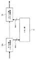
図8は、上記変換関数を用いて消費電力を最適化する制御部4を含んだ回路の一例である。上記式(1)に示した直前のトランザクションTi-1と送信対象のトランザクションTiとの変換関数を利用したハミング距離dH(Ti-1、変換関数(Ti))を利用するには、当該変換関数をスレーブ側でも持つ必要がある。上記ステップS3のトランザクションデータ解析処理の結果から、上記式(1)が最初になる変換関数を選択する。図8において、マスタ側データ変換回路8mでは、その変換関数を実現している。このとき、スレーブ側では復元するための情報が必要となるため、マスタ側制御部4mは、復元するための情報として復元情報Sg1をスレーブ側制御部4sへ送る。スレーブ側制御部4sは、受け取った復元情報Sg1をスレーブ側データ復元回路9sに送り、当該スレーブ側データ復元回路9sにて、マスタ側データ変換回路8mから送られたデータを復元する。本回路構成により、バスの電力は最適化される。FIG. 8 is an example of a circuit including a
図9および図10を参照して、上記変換関数として、固定長のビット反転を利用した場合の一例を説明する。なお、図9は、固定長のビット反転を利用した変換関数を用いて消費電力を最適化する制御部4を含んだ回路の一例である。図10は、固定長のビット反転とトグル数との関係を示す図である。 With reference to FIG. 9 and FIG. 10, an example in which fixed-length bit inversion is used as the conversion function will be described. FIG. 9 is an example of a circuit including the
図10(a)に示すように、前トランザクションデータT1「0100 0001 1110 0000」が送信された後、次のトランザクションデータT2「1011 1110 0001 1110」をそのまま送信した場合、トグル数は「15」となる。ここで、トランザクションデータT2も対してビット反転を行うと、トランザクションデータT2は、「0100 0001 1110 0001」となる。このビット反転によって、マスタとスレーブとの間では、反転信号が1ビット増えるが、トランザクションとしてのトグル数が「1」となる。 As shown in FIG. 10A, when the previous transaction data T1 “0100 0001 1110 0000” is transmitted and then the next transaction data T2 “1011 1110 0001 1110” is transmitted as it is, the number of toggles is “15”. Become. If bit inversion is performed on the transaction data T2 as well, the transaction data T2 becomes “0100 0001 1110 0001”. By this bit inversion, the inversion signal increases by 1 bit between the master and the slave, but the number of toggles as a transaction becomes “1”.
また、図10(b)に示すように、前トランザクションデータT3「0100 0001 1110 0000」が送信された後、次のトランザクションデータT4「0111 0101 0010 0101」をそのまま送信した場合、トグル数は「7」となる。そして、トランザクションデータT4に対してビット反転を行うと、トランザクションデータT4は、「1000 1010 1101 1010」となり、ビット反転によるトグル数が「9」となる。つまり、この場合は、ビット反転を行わずにそのまま送信することで、トグル数を送信ビット数以下に抑えられる。 Further, as shown in FIG. 10B, when the previous transaction data T3 “0100 0001 1110 0000” is transmitted and then the next transaction data T4 “0111 0101 0010 0101” is transmitted as it is, the number of toggles is “7”. " When bit inversion is performed on the transaction data T4, the transaction data T4 becomes “1000 1010 1101 1010”, and the number of toggles by bit inversion becomes “9”. That is, in this case, the number of toggles can be suppressed to the number of transmission bits or less by transmitting as it is without performing bit inversion.
ここで、上記変換関数としてトランザクションデータがビット反転に適するか否かは、上記ステップS3におけるトランザクションデータ解析処理で判断する。具体的には、図9において、マスタ側制御部4mは、前トランザクションデータを保有しており、当該前トランザクションと、次に送る予定のトランザクションとのハミング距離を計算する。そして、相対的にハミング距離が大きければ、上述した固定長のビット反転を転送データに施すために、マスタ側制御部4mからマスタ側ビット反転回路8maおよびスレーブ側ビット反転回路9saへビット反転指示信号Sg1aをアクティブにする。ビット反転回路8maは、送信する予定のトランザクションデータをビット反転して、スレーブ側ビット反転回路9saへ送出する。スレーブ側ビット反転回路9saでは、受け取ったデータをビット反転指示信号Sg1aに応じて処理する。 Here, whether or not the transaction data is suitable for bit inversion as the conversion function is determined by the transaction data analysis processing in step S3. Specifically, in FIG. 9, the master-
以上では、ハードウエアのみによる上記変換関数の実装を説明したが、CPU1で動作するソフトウエア50に、トランザクションAPI51を組み込む(図4参照)ことで当該変換関数を利用してもかまわない。CPU1上で動作するソフトウエア50がトランザクションAPI51を用いてデータ転送を行う場合、トランザクションAPI51内部でトランザクションに最適な変換関数を選択し、その変換関数を利用するようにトランザクションAPI51内部で制御部4へ伝達することで、ソフトウエア50を用いた動的な変換関数の選択ができる。動的な変換関数は、マスタ側制御部4mおよびスレーブ側制御部4sでそれぞれ実装することで実現することができる。 In the above, the implementation of the conversion function using only hardware has been described. However, the conversion function may be used by incorporating the
次に、図11を参照して、上記変換関数として、可変長のビット反転を利用した場合の一例を説明する。なお、図11は、可変長のビット反転とトグル数との関係を示す図である。 Next, an example in which variable-length bit inversion is used as the conversion function will be described with reference to FIG. FIG. 11 is a diagram showing the relationship between variable-length bit inversion and the number of toggles.
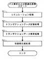
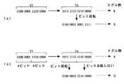
図11(a)に示すように、前トランザクションデータT5「0100 0001 1110 0000」が送信された後、次のトランザクションデータT6「1011 1110 1110 0000」をそのまま送信した場合、トグル数は「8」となる。そして、トランザクションデータT6全体に対してビット反転を行うと、トランザクションデータT6は、「0100 0001 0001 1111」となり、ビット反転によるトグル数が「8」となり、さらに、マスタとスレーブと間での反転信号が1ビット増える。つまり、この場合、反転することによってトグル数が変わらず反転信号が1ビット増えるため、ビット反転せずに転送した方がよいことになる。 As shown in FIG. 11A, when the next transaction data T6 “1011 1110 1110 0000” is transmitted as it is after the previous transaction data T5 “0100 0001 1110 0000” is transmitted, the number of toggles is “8”. Become. When bit inversion is performed on the entire transaction data T6, the transaction data T6 becomes “0100 0001 0001 1111”, the number of toggles by bit inversion becomes “8”, and an inverted signal between the master and slave Increases by one bit. In other words, in this case, since the number of toggles does not change and the number of inverted signals increases by 1 bit by inversion, it is better to transfer without inversion of bits.
しかしながら、図11(b)に示すように、16ビットのビット列で構成されるトランザクションデータT6を8ビット毎に分割し、前半のビット列を反転、後半のビット列を反転しない場合、トグル数が「8」から「0」に減少する。ここで、これら8ビット毎に分割すると仮定した場合、ビット分割を実行したことを示す情報1ビットおよび反転の実行の有無を示す情報2ビットの合計3ビットが別に必要になる。 However, as shown in FIG. 11B, when the transaction data T6 composed of a 16-bit bit string is divided every 8 bits, the first bit string is inverted, and the latter bit string is not inverted, the toggle number is “8”. To "0". Here, if it is assumed that the data is divided every 8 bits, a total of 3 bits are required, that is, 1 information bit indicating that bit division is performed and 2 information bits indicating whether or not to perform inversion.
ここで、上記変換関数としてトランザクションデータのビットを分割し、分割群毎にビット反転するか否かの判断は、上記ステップS3におけるトランザクションデータ解析処理で判断する。具体的には、図9において、マスタ側制御部4mは、前トランザクションデータを保有しており、当該前トランザクションと、次に送る予定のトランザクションを複数のビット幅に分割してそれぞれの分割に応じたハミング距離を計算する。そして、マスタ側制御部4mは、ハミング距離が一番小さくなる分割を選択する。分割方式が決まれば、分割群毎に相対的にハミング距離が大きければビット反転を転送データに施すために、マスタ側制御部4mからマスタ側ビット反転回路8maおよびスレーブ側ビット反転回路9saへビット反転指示信号Sg1aをアクティブにする。ビット反転回路8maは、送信する予定のトランザクションデータをビット反転して、スレーブ側ビット反転回路9saへ送出する。スレーブ側ビット反転回路9saでは、受け取ったデータをビット反転指示信号Sg1aに応じて処理する。 Here, it is determined in the transaction data analysis process in step S3 whether the bit of transaction data is divided as the conversion function and the bit is inverted for each divided group. Specifically, in FIG. 9, the master-
以上では、ハードウエアのみによる上記変換関数の実装を説明したが、CPU1で動作するソフトウエア50に、トランザクションAPI51を組み込む(図4参照)ことで当該変換関数を利用してもかまわない。CPU1上で動作するソフトウエア50がトランザクションAPI51を用いてデータ転送を行う場合、トランザクションAPI51内部でトランザクションに最適な変換関数を選択し、その変換関数を利用するようにトランザクションAPI51内部で制御部4へ伝達することで、ソフトウエア50を用いた動的な変換関数の選択ができる。動的な変換関数は、マスタ側制御部4mおよびスレーブ側制御部4sでそれぞれ実装することで実現することができる。 In the above, the implementation of the conversion function using only hardware has been described. However, the conversion function may be used by incorporating the
また、バスの消費電力を最適化する別の施策として、当該バスで転送するデータ量を少なくすることが考えられる。図12および図13を参照して、トランザクションデータから、より少ないビット数で全トランザクションを転送する一例を説明する。なお、図12は、上記少ないビット数で転送することによって消費電力を最適化する制御部4を含んだ回路の一例である。図13は、通信量を減らすための一意に復号可能なトランザクションデータTに対する符号化例を示す図である。 Further, as another measure for optimizing the power consumption of the bus, it is conceivable to reduce the amount of data transferred by the bus. With reference to FIGS. 12 and 13, an example of transferring all transactions from transaction data with a smaller number of bits will be described. FIG. 12 is an example of a circuit including the
図13に示すトランザクションデータTの例は、符号長が全て2であり、それらのデータには特定の出現する偏りが存在する。具体的には、トランザクションデータTが「00」の出現率は、80%である。トランザクションデータTが「01」の出現率は、13%である。トランザクションデータTが「10」の出現率は、5%である。そして、トランザクションデータTが「11」の出現率は、2%である。 In the example of the transaction data T shown in FIG. 13, the code lengths are all 2, and there is a specific appearance bias in those data. Specifically, the appearance rate when the transaction data T is “00” is 80%. The appearance rate when the transaction data T is “01” is 13%. The appearance rate when the transaction data T is “10” is 5%. The appearance rate when the transaction data T is “11” is 2%.
このとき、それぞれのトランザクションTに、図13に示す符号を割り当てる。具体的には、トランザクションデータTが「00」に1ビットの符号「0」を割り当てる。トランザクションデータTが「01」に2ビットの符号「01」を割り当てる。トランザクションデータTが「10」に3ビットの符号「001」を割り当てる。そして、トランザクションデータTが「11」に3ビットの符号「000」を割り当てる。この例における、符号化前後の転送量は、2ビット×100%:1ビット×80%+2ビット×13%+3ビット×5%+3ビット×2%=200:127となり、約4割近くデータ量を削減できる。その結果として、電力削減につながる。 At this time, a code shown in FIG. 13 is assigned to each transaction T. Specifically, a 1-bit code “0” is assigned to the transaction data T “00”. A 2-bit code “01” is assigned to the transaction data T “01”. A 3-bit code “001” is assigned to the transaction data T “10”. Then, a 3-bit code “000” is assigned to the transaction data T “11”. In this example, the transfer amount before and after encoding is 2 bits × 100%: 1 bit × 80% + 2 bits × 13% + 3 bits × 5% + 3 bits × 2% = 200: 127, and the data amount is about 40%. Can be reduced. As a result, it leads to power reduction.
図12において、マスタ側符号化回路10mは、上述した符号化を行いスレーブ側復号化回路11sに送信し、データ量に関して最適なトランザクションを送信する回路を構成する。マスタ側制御部4mは、上記ステップS3のトランザクションデータ解析処理の結果から、最適な符号化方式が決まり、当該符号化方式に基づいて変換テーブル(例えば図13参照)を作成する。そして、上記変換テーブルを用いた符号化および復号化処理をマスタ側符号化回路10mおよびスレーブ側復号化回路11sがそれぞれ行う。 In FIG. 12, the master
このとき、上記ステップS1で用いたデータ以外からなるトランザクションの場合、上記変換テーブルでは最適な符号化が行なわれない可能性がある。そこで、CPU1で動作し、トランザクションAPI51を用いたソフトウエア50(図4参照)にて、データ転送開始時に最適な符号化を計算し、新たな変換テーブルを作成後、その変換テーブルをマスタ側制御部4mに転送することで、動的に変換テーブルを変更し最適な変換テーブルを作成できる。また、変換テーブルを変更する処理全てをソフトウエアで実現した場合や性能に与えるインパクトが大きな場合、事前に数種類の変換テーブルを用意し、それらを切り替えても本発明を実現可能であり、このような変換テーブルの変更方法も、本発明の対象に含まれる。 At this time, in the case of a transaction composed of data other than the data used in step S1, there is a possibility that optimal encoding is not performed in the conversion table. Therefore, the
次に、図14を参照して、入力および出力のバス幅が異なる記憶装置を介してトランザクションを転送する装置の一例について説明する。なお、図14は、入力のバス幅BW1および出力のバス幅BW2となったメモリ部13を介してトランザクションを転送する装置のブロック図である。 Next, an example of a device that transfers a transaction via storage devices having different input and output bus widths will be described with reference to FIG. FIG. 14 is a block diagram of an apparatus for transferring a transaction via the
図14において、入出力双方でバッファを設けず、それぞれにマスタ側メモリ制御部12mおよびスレーブ側メモリ制御部12sを備え、メモリ部13を共有することで、スレーブ側が所望のタイミングでメモリ部13に格納されたデータを利用できるようになる。マスタ側およびスレーブ側にとって最適なタイミングは、上記ステップS3のトランザクションデータ解析処理にて性能解析を行うことでデータが必要なタイミングを解析し、当該タイミングに余裕があれば、データサイズと消費電力との関係(図5参照)を考慮し、図14に示す構成回路を利用することで、バスの最適化が図られる。また、図6または図7で示した構成を図14に示した回路構成に組み合わせることで、動的にビット幅を変更することも可能となる。また、バス幅変更もハードウエアとソフトウエアで制御する方法があり、双方とも本発明から構成される回路の一例である。なお、本実施例では、記憶装置をメモリ部13で説明したが、本発明で述べるところの記憶装置は、レジスタやFIFO等も含まれる。また、図14では、メモリ部13に対して異なるポートを形成しているが、マスタ側およびスレーブ側で共通のポートを用いてもかまわない。 In FIG. 14, buffers are not provided for both input and output, and each includes a master-side
また、バスの消費電力を最適化する別の施策として、動作周波数を低くすることが考えられる。図15を参照して、動作周波数を低くすることによってバスの消費電力を最適化する一例を説明する。なお、図15は、動作周波数を動的に変更させる半導体集積回路装置の一例である。 Further, as another measure for optimizing the bus power consumption, it is conceivable to lower the operating frequency. With reference to FIG. 15, an example of optimizing bus power consumption by lowering the operating frequency will be described. FIG. 15 is an example of a semiconductor integrated circuit device that dynamically changes the operating frequency.
図15において、マスタ側クロック制御部14mにて、ベースとなる入力クロック信号Sg3のクロック周期を変化させたクロックまたは同一のクロックを、マスタ側データ送信回路15mおよびスレーブ側データ受信回路16sへクロック信号Sg4として伝播させる。クロック信号Sg4を受け取ったマスタ側データ送信回路15mおよびスレーブ側データ受信回路16sは、それぞれ回路が動作するクロック信号Sg4の周期に応じて動作する。 In FIG. 15, the master side
図16に、ハードウエアのみでクロックを動的に変更するマスタ側クロック制御部14mの一例を示す。図16において、マスタ側クロック制御部14mの中には、カウンタ141mが備えられている。マスタ側クロック制御部14mは、カウンタ141mに設定されたベースカウンタ値分、分周することができる。分周させない場合、マスタ側クロック制御部14mは、入力クロック信号Sg3をそのまま出力してもかまわない。 FIG. 16 shows an example of the master side
転送が開始されると、マスタ側クロック制御部14mには、バスからトランザクション転送開始信号Sg5が送られてくる。なお、トランザクション転送開始信号Sg5を用いなくても、トランザクション記憶部5(図3参照)で用いた方法と同様の構成によって、バスからトランザクションが生成されるので、この構成を用いてもかまわない。トランザクション転送開始信号Sg5が送られた場合、マスタ側クロック制御部14mは、カウンタ141mで参照するベースカウンタ値を減らすことで、動作周波数を高くすることができる。そして、マスタ側クロック制御部14mは、バスからマスタ側トランザクション転送終了信号Sg6を検出すると、カウンタ141mのベースカウンタ値を増やすことで、周波数を低くすることができる。このように、マスタ側クロック制御部14mは、トランザクションの増減に応じて周波数を変更するため、適切な周波数が動的に選択される。 When the transfer is started, a transaction transfer start signal Sg5 is sent from the bus to the master side
図17に、周波数変更手段をソフトウエア実現するマスタ側クロック制御部14mの一例を示す。図17において、マスタ側クロック制御部14mの中には、カウンタ142mが形成される。 FIG. 17 shows an example of the master side
CPU1上で動作するソフトウエア50で利用するトランザクションAPI51(図4参照)において、トランザクション開始前に制御部4へ転送開始を知らせることで、図17におけるマスタ側クロック制御部14mに入力するマスタ側クロック制御信号Sg7を変化させる。つまり、マスタ側クロック制御信号Sg7は、マスタ側トランザクション転送開始信号Sg5(図16参照)と同様の役割を担っており、これによって、マスタ側クロック制御部14mが同様に動的にクロック周波数を変更する回路を構成することができる。 In the transaction API 51 (see FIG. 4) used by the
なお、図17の一例では、制御部4経由でマスタ側クロック制御部14mへのマスタ側クロック制御信号Sg7を生成しているが、CPU1から直接ソフトウエアでマスタ側クロック制御部14mを制御することも、可能であり、そのように回路を構成してもかまわない。 In the example of FIG. 17, the master-side clock control signal Sg7 is generated to the master-side
また、上述した半導体集積装置の設計方法は、コンピュータにそれぞれのステップを実行させる半導体集積装置の設計プログラムとしても実現可能である。また、この設計プログラムは、上記コンピュータが読取可能な記録媒体(光ディスク、磁気ディスク、メモリーカードなど)に格納することが可能である。さらに、上記設計プログラムは、他の媒体や通信回線を通じて供給することもできる。 The above-described semiconductor integrated device design method can also be implemented as a semiconductor integrated device design program that causes a computer to execute each step. The design program can be stored in a computer-readable recording medium (optical disk, magnetic disk, memory card, etc.). Furthermore, the design program can be supplied through other media or communication lines.
本発明の半導体集積装置の設計方法および設計プログラムは、トランザクションデータを用いてオンチップバスを大局的に性能および電力の最適化が可能となり、半導体集積回路装置のオンチップバス構造の設計や検討などへ適用することができる。 The design method and design program for a semiconductor integrated device according to the present invention makes it possible to optimize the performance and power of an on-chip bus globally using transaction data, and to design and examine the on-chip bus structure of a semiconductor integrated circuit device. Can be applied to.
1…CPU
2…メモリ
3…ハードウエア
4…制御部
5…トランザクション記憶部
6…バッファ
7…セレクタ
8…データ変換回路
9…データ復元回路
10…符号化回路
11…復号化回路
12…メモリ制御部
13…メモリ部
14…クロック制御部
141、142…カウンタ
15…データ送信回路
16…データ受信回路
50…ソフトウエア
51…トランザクションAPI
60…トランザクションデータ1 ... CPU
DESCRIPTION OF
60 ... Transaction data
Claims (16)
Translated fromJapanese前記半導体集積装置の動作を模擬したシミュレーションを実行する工程と、
前記シミュレーションを実行する工程で得られた前記バス上を流れるデータビット系列を、当該バスのプロトコルに応じて意味のある1つ以上のビット系列に分類してトランザクションデータとして記憶する工程と、
前記トランザクションデータを解析し、前記バスを所定の条件に基づいて制御する制御部を生成する工程とを含むことを特徴とする、半導体集積装置の設計方法。A semiconductor integrated device design method for designing a semiconductor integrated device in which functional blocks are interconnected by a bus,
Performing a simulation simulating the operation of the semiconductor integrated device;
Classifying the data bit stream flowing on the bus obtained in the step of executing the simulation into one or more meaningful bit series according to the protocol of the bus and storing it as transaction data;
Analyzing the transaction data, and generating a control unit that controls the bus based on a predetermined condition.
前記トランザクションデータから前記バスのバス幅を一意に決定する前記制御部を生成し、
前記バス幅を選択するセレクタを設定する工程を含むことを特徴とする、請求項1に記載の半導体集積装置の設計方法。The step of generating the control unit includes:
Generating the control unit for uniquely determining the bus width of the bus from the transaction data;
2. The method for designing a semiconductor integrated device according to claim 1, further comprising a step of setting a selector for selecting the bus width.
前記トランザクションデータの特徴に応じて、前記バスのバス幅を動的に決定する前記制御部を生成し、
前記バス幅を選択するセレクタを設定する工程を含むことを特徴とする、請求項1に記載の半導体集積装置の設計方法。The step of generating the control unit includes:
Generate the control unit that dynamically determines the bus width of the bus according to the characteristics of the transaction data,
2. The method for designing a semiconductor integrated device according to claim 1, further comprising a step of setting a selector for selecting the bus width.
前記トランザクションデータのうち連続する固定長ビット列間でビットごとの変化が最も少なくなるようなビット列を選択し、
前記トランザクションデータのうち前記選択されたビット列を最もビットごとの変化が少なくなるように変換し、
前記変換されたビット列を当該変換前のビット列に復元するための情報を付加するように前記バスを制御する前記制御部を生成することを特徴とする、請求項1に記載の半導体集積装置の設計方法。In the step of generating the control unit,
Select a bit string that minimizes the change of each bit between fixed-length bit strings that are continuous among the transaction data,
The selected bit string of the transaction data is converted so as to minimize the change for each bit,
The design of the semiconductor integrated device according to claim 1, wherein the control unit that controls the bus is added so as to add information for restoring the converted bit string to the bit string before the conversion. Method.
前記トランザクションデータのうち連続する可変長ビット列間でビットごとの変化が最も少なくなるようなビット列および当該ビット列の長さを選択し、
前記トランザクションデータのうち最もビットごとの変化が少なくなるように前記ビット列の長さで前記選択されたビット列を変換し、
前記変換されたビット列を当該変換前のビット列に復元するための情報を付加するように前記バスを制御する前記制御部を生成することを特徴とする、請求項1に記載の半導体集積装置の設計方法。In the step of generating the control unit,
Select a bit string and the length of the bit string that minimize the change for each bit between continuous variable-length bit strings in the transaction data,
Converting the selected bit string with the length of the bit string so that the change of each bit of the transaction data is minimized;
The design of the semiconductor integrated device according to claim 1, wherein the control unit that controls the bus is added so as to add information for restoring the converted bit string to the bit string before the conversion. Method.
前記トランザクションデータの種類ごとにその出現率を計測し、
前記出現率が相対的に高い前記トランザクションデータのビット列を、当該ビット列より少ないビット列に一意に変換するための変換テーブルを生成し、
前記変換テーブルに基づいて、前記トランザクションデータのビット列を変換するように前記バスを制御する前記制御部を生成することを特徴とする、請求項1に記載の半導体集積装置の設計方法。In the step of generating the control unit,
Measure the appearance rate for each type of transaction data,
Generating a conversion table for uniquely converting a bit string of the transaction data having a relatively high appearance rate into a bit string smaller than the bit string;
2. The method of designing a semiconductor integrated device according to claim 1, wherein the control unit that controls the bus so as to convert a bit string of the transaction data is generated based on the conversion table.
前記変換テーブルは、前記ソフトウエアによって動的に変更されることを特徴とする、請求項10記載の半導体集積装置の設計方法。The control unit stores the conversion table by software executed by a central processing unit connected to the bus,
11. The method of designing a semiconductor integrated device according to claim 10, wherein the conversion table is dynamically changed by the software.
前記コンピュータに、
前記半導体集積装置の動作を模擬したシミュレーションを実行するステップと、
前記シミュレーションを実行するステップで得られた前記バス上を流れるデータビット系列を、当該バスのプロトコルに応じて意味のある1つ以上のビット系列に分類してトランザクションデータとして記憶するステップと、
前記トランザクションデータを解析し、前記バスを所定の条件に基づいて制御する制御部を生成するステップとを実行させることを特徴とする、半導体集積装置の設計プログラム。A program for designing a semiconductor integrated device to be executed by a computer that designs a semiconductor integrated device having functional blocks interconnected by a bus,
In the computer,
Executing a simulation simulating the operation of the semiconductor integrated device;
Classifying the data bit stream flowing on the bus obtained in the step of executing the simulation into one or more meaningful bit series according to the protocol of the bus and storing it as transaction data;
Analyzing the transaction data, and generating a control unit for controlling the bus based on a predetermined condition. 7. A design program for a semiconductor integrated device, comprising:
前記コンピュータに、
前記半導体集積装置の動作を模擬したシミュレーションを実行するステップと、
前記シミュレーションを実行するステップで得られた前記バス上を流れるデータビット系列を、当該バスのプロトコルに応じて意味のある1つ以上のビット系列に分類してトランザクションデータとして記憶するステップと、
前記トランザクションデータを解析し、前記バスを所定の条件に基づいて制御する制御部を生成するステップとを実行させることを特徴とする、半導体集積装置の設計プログラムを記録した記録媒体。A recording medium recording a design program of a semiconductor integrated device to be executed by a computer that designs a semiconductor integrated device in which functional blocks are interconnected by a bus,
In the computer,
Executing a simulation simulating the operation of the semiconductor integrated device;
Classifying the data bit stream flowing on the bus obtained in the step of executing the simulation into one or more meaningful bit series according to the protocol of the bus and storing it as transaction data;
And a step of generating a control unit for analyzing the transaction data and controlling the bus based on a predetermined condition. A recording medium recording a design program for a semiconductor integrated device.
Priority Applications (4)
| Application Number | Priority Date | Filing Date | Title |
|---|---|---|---|
| JP2004178372AJP2006004076A (en) | 2004-06-16 | 2004-06-16 | Semiconductor integrated device design method, design program, and recording medium |
| US11/148,321US20050283349A1 (en) | 2004-06-16 | 2005-06-09 | Design method, design program, and storage medium for semiconductor integrated device |
| EP05012581AEP1607886A3 (en) | 2004-06-16 | 2005-06-10 | Design method and program for a bus control portion in a semiconductor integrated device |
| CNA2005100781914ACN1713369A (en) | 2004-06-16 | 2005-06-16 | Design method, design program and storage medium for semiconductor integrated device |
Applications Claiming Priority (1)
| Application Number | Priority Date | Filing Date | Title |
|---|---|---|---|
| JP2004178372AJP2006004076A (en) | 2004-06-16 | 2004-06-16 | Semiconductor integrated device design method, design program, and recording medium |
Publications (1)
| Publication Number | Publication Date |
|---|---|
| JP2006004076Atrue JP2006004076A (en) | 2006-01-05 |
Family
ID=35094345
Family Applications (1)
| Application Number | Title | Priority Date | Filing Date |
|---|---|---|---|
| JP2004178372AWithdrawnJP2006004076A (en) | 2004-06-16 | 2004-06-16 | Semiconductor integrated device design method, design program, and recording medium |
Country Status (4)
| Country | Link |
|---|---|
| US (1) | US20050283349A1 (en) |
| EP (1) | EP1607886A3 (en) |
| JP (1) | JP2006004076A (en) |
| CN (1) | CN1713369A (en) |
Cited By (1)
| Publication number | Priority date | Publication date | Assignee | Title |
|---|---|---|---|---|
| US9195095B2 (en) | 2007-07-29 | 2015-11-24 | Cree, Inc. | LED lighting devices incorporating waveguides |
Families Citing this family (3)
| Publication number | Priority date | Publication date | Assignee | Title |
|---|---|---|---|---|
| EP2294770B1 (en)* | 2008-06-20 | 2013-08-07 | Rambus, Inc. | Frequency responsive bus coding |
| KR20120046461A (en)* | 2010-11-02 | 2012-05-10 | 삼성전자주식회사 | Interface device and system including the same |
| US10540304B2 (en)* | 2017-04-28 | 2020-01-21 | Advanced Micro Devices, Inc. | Power-oriented bus encoding for data transmission |
Family Cites Families (9)
| Publication number | Priority date | Publication date | Assignee | Title |
|---|---|---|---|---|
| US5349542A (en)* | 1992-04-02 | 1994-09-20 | Vlsi Technology, Inc. | Method for sizing widths of power busses in integrated circuits |
| US6304930B1 (en)* | 1998-01-20 | 2001-10-16 | Matsushita Electric Industrial Co., Ltd. | Signal transmission system having multiple transmission modes |
| JP2001142927A (en)* | 1999-11-16 | 2001-05-25 | Matsushita Electric Ind Co Ltd | Semiconductor integrated circuit device design method, circuit power consumption analysis method, and power consumption analysis device |
| JP2001142928A (en)* | 1999-11-16 | 2001-05-25 | Matsushita Electric Ind Co Ltd | Design method of semiconductor integrated circuit device |
| EP1150467A1 (en)* | 2000-04-28 | 2001-10-31 | STMicroelectronics S.r.l. | Encoder architecture for parallel busses |
| GB2378537A (en)* | 2001-08-10 | 2003-02-12 | At & T Lab Cambridge Ltd | Power reduction in microprocessor systems |
| US20030088799A1 (en)* | 2001-11-05 | 2003-05-08 | Bodas Devadatta V. | Method and apparatus for regulation of electrical component temperature and power consumption rate through bus width reconfiguration |
| GB2385688A (en)* | 2002-02-26 | 2003-08-27 | Nec Technologies | Minimising power loss in addressing memory |
| JP2003332443A (en)* | 2002-05-08 | 2003-11-21 | Toshiba Corp | Semiconductor integrated circuit, design support apparatus therefor, and test method |
- 2004
- 2004-06-16JPJP2004178372Apatent/JP2006004076A/ennot_activeWithdrawn
- 2005
- 2005-06-09USUS11/148,321patent/US20050283349A1/ennot_activeAbandoned
- 2005-06-10EPEP05012581Apatent/EP1607886A3/ennot_activeWithdrawn
- 2005-06-16CNCNA2005100781914Apatent/CN1713369A/enactivePending
Cited By (1)
| Publication number | Priority date | Publication date | Assignee | Title |
|---|---|---|---|---|
| US9195095B2 (en) | 2007-07-29 | 2015-11-24 | Cree, Inc. | LED lighting devices incorporating waveguides |
Also Published As
| Publication number | Publication date |
|---|---|
| CN1713369A (en) | 2005-12-28 |
| EP1607886A3 (en) | 2006-03-22 |
| US20050283349A1 (en) | 2005-12-22 |
| EP1607886A2 (en) | 2005-12-21 |
Similar Documents
| Publication | Publication Date | Title |
|---|---|---|
| JP3888070B2 (en) | Logic circuit module having power consumption control interface and storage medium storing the module | |
| US8069274B2 (en) | System and method for serial data communications between host and communications devices, and communications device employed in the system and method | |
| US7412670B2 (en) | Method and apparatus for optimizing distributed multiplexed bus interconnects | |
| CN101132336A (en) | Heterogeneous multi-core processor high-speed asynchronous interconnection communication network | |
| CN102279724A (en) | Power-efficient sign extension for booth multiplication methods and systems | |
| US20080155353A1 (en) | Data processing apparatus and method for reducing trace bandwidth | |
| US6834378B2 (en) | System on a chip bus with automatic pipeline stage insertion for timing closure | |
| CN101384989B (en) | Method and system for performing Booth multiplication in a digital signal processor | |
| Ramagond et al. | A review and analysis of communication logic between PL and PS in ZYNQ AP SoC | |
| JPH117427A (en) | Asynchronous digital system, asynchronous data pass circuit asynchronous digital signal processing circuit, and asynchronous digital signal processing method | |
| US8181130B1 (en) | Method for jitter reduction by shifting current consumption | |
| CN102411555B (en) | A Scalable Dynamically Reconfigurable Array Configuration Information Method | |
| JP2006004076A (en) | Semiconductor integrated device design method, design program, and recording medium | |
| TWI813001B (en) | Accelerating method of executing comparison functions and accelerating system of executing comparison functions | |
| CN205176827U (en) | Two synchronous electronic equipment with symbol is instructed in proruption | |
| US20040128634A1 (en) | Method, system, and product for achieving optimal timing in a data path that includes variable delay lines and coupled endpoints | |
| CN103443738A (en) | Method and corresponding computer program product for ranking paths to power optimize integrated circuit design | |
| JP6570046B2 (en) | DMA controller, realization method and computer storage medium | |
| JP7259961B2 (en) | High-level synthesis device, high-level synthesis method and program | |
| US10482208B2 (en) | Coding and synthesizing a state machine in state groups | |
| CN114462337A (en) | Synthesis method and device, device and storage medium of sequential logic | |
| Tsao et al. | Parameterized and low power DSP core for embedded systems | |
| Salman et al. | High Performance and Low Power Axi-Lite 4 Master Controller Using System Verilog | |
| US20240111694A1 (en) | Node identification allocation in a multi-tile system with multiple derivatives | |
| Mallikarjunaswamy et al. | Design of Advanced High-Performance Bus Master to Access a SRAM Block |
Legal Events
| Date | Code | Title | Description |
|---|---|---|---|
| A621 | Written request for application examination | Free format text:JAPANESE INTERMEDIATE CODE: A621 Effective date:20070227 | |
| A761 | Written withdrawal of application | Free format text:JAPANESE INTERMEDIATE CODE: A761 Effective date:20080630 |