JP2005530335A - Process and system for heating a semiconductor substrate in a processing chamber including a susceptor - Google Patents
Process and system for heating a semiconductor substrate in a processing chamber including a susceptorDownload PDFInfo
- Publication number
- JP2005530335A JP2005530335AJP2004504278AJP2004504278AJP2005530335AJP 2005530335 AJP2005530335 AJP 2005530335AJP 2004504278 AJP2004504278 AJP 2004504278AJP 2004504278 AJP2004504278 AJP 2004504278AJP 2005530335 AJP2005530335 AJP 2005530335A
- Authority
- JP
- Japan
- Prior art keywords
- wafer
- susceptor
- support structure
- semiconductor wafer
- support
- Prior art date
- Legal status (The legal status is an assumption and is not a legal conclusion. Google has not performed a legal analysis and makes no representation as to the accuracy of the status listed.)
- Granted
Links
Images


Classifications
- H—ELECTRICITY
- H01—ELECTRIC ELEMENTS
- H01L—SEMICONDUCTOR DEVICES NOT COVERED BY CLASS H10
- H01L21/00—Processes or apparatus adapted for the manufacture or treatment of semiconductor or solid state devices or of parts thereof
- H01L21/02—Manufacture or treatment of semiconductor devices or of parts thereof
- H01L21/04—Manufacture or treatment of semiconductor devices or of parts thereof the devices having potential barriers, e.g. a PN junction, depletion layer or carrier concentration layer
- H01L21/18—Manufacture or treatment of semiconductor devices or of parts thereof the devices having potential barriers, e.g. a PN junction, depletion layer or carrier concentration layer the devices having semiconductor bodies comprising elements of Group IV of the Periodic Table or AIIIBV compounds with or without impurities, e.g. doping materials
- H01L21/30—Treatment of semiconductor bodies using processes or apparatus not provided for in groups H01L21/20 - H01L21/26
- H01L21/324—Thermal treatment for modifying the properties of semiconductor bodies, e.g. annealing, sintering
- H—ELECTRICITY
- H01—ELECTRIC ELEMENTS
- H01L—SEMICONDUCTOR DEVICES NOT COVERED BY CLASS H10
- H01L21/00—Processes or apparatus adapted for the manufacture or treatment of semiconductor or solid state devices or of parts thereof
- H01L21/67—Apparatus specially adapted for handling semiconductor or electric solid state devices during manufacture or treatment thereof; Apparatus specially adapted for handling wafers during manufacture or treatment of semiconductor or electric solid state devices or components ; Apparatus not specifically provided for elsewhere
- H01L21/67005—Apparatus not specifically provided for elsewhere
- H01L21/67011—Apparatus for manufacture or treatment
- H01L21/67098—Apparatus for thermal treatment
- H01L21/67103—Apparatus for thermal treatment mainly by conduction
- C—CHEMISTRY; METALLURGY
- C23—COATING METALLIC MATERIAL; COATING MATERIAL WITH METALLIC MATERIAL; CHEMICAL SURFACE TREATMENT; DIFFUSION TREATMENT OF METALLIC MATERIAL; COATING BY VACUUM EVAPORATION, BY SPUTTERING, BY ION IMPLANTATION OR BY CHEMICAL VAPOUR DEPOSITION, IN GENERAL; INHIBITING CORROSION OF METALLIC MATERIAL OR INCRUSTATION IN GENERAL
- C23C—COATING METALLIC MATERIAL; COATING MATERIAL WITH METALLIC MATERIAL; SURFACE TREATMENT OF METALLIC MATERIAL BY DIFFUSION INTO THE SURFACE, BY CHEMICAL CONVERSION OR SUBSTITUTION; COATING BY VACUUM EVAPORATION, BY SPUTTERING, BY ION IMPLANTATION OR BY CHEMICAL VAPOUR DEPOSITION, IN GENERAL
- C23C16/00—Chemical coating by decomposition of gaseous compounds, without leaving reaction products of surface material in the coating, i.e. chemical vapour deposition [CVD] processes
- C23C16/44—Chemical coating by decomposition of gaseous compounds, without leaving reaction products of surface material in the coating, i.e. chemical vapour deposition [CVD] processes characterised by the method of coating
- C23C16/458—Chemical coating by decomposition of gaseous compounds, without leaving reaction products of surface material in the coating, i.e. chemical vapour deposition [CVD] processes characterised by the method of coating characterised by the method used for supporting substrates in the reaction chamber
- C23C16/4582—Rigid and flat substrates, e.g. plates or discs
- C23C16/4583—Rigid and flat substrates, e.g. plates or discs the substrate being supported substantially horizontally
- C23C16/4585—Devices at or outside the perimeter of the substrate support, e.g. clamping rings, shrouds
- C—CHEMISTRY; METALLURGY
- C23—COATING METALLIC MATERIAL; COATING MATERIAL WITH METALLIC MATERIAL; CHEMICAL SURFACE TREATMENT; DIFFUSION TREATMENT OF METALLIC MATERIAL; COATING BY VACUUM EVAPORATION, BY SPUTTERING, BY ION IMPLANTATION OR BY CHEMICAL VAPOUR DEPOSITION, IN GENERAL; INHIBITING CORROSION OF METALLIC MATERIAL OR INCRUSTATION IN GENERAL
- C23C—COATING METALLIC MATERIAL; COATING MATERIAL WITH METALLIC MATERIAL; SURFACE TREATMENT OF METALLIC MATERIAL BY DIFFUSION INTO THE SURFACE, BY CHEMICAL CONVERSION OR SUBSTITUTION; COATING BY VACUUM EVAPORATION, BY SPUTTERING, BY ION IMPLANTATION OR BY CHEMICAL VAPOUR DEPOSITION, IN GENERAL
- C23C16/00—Chemical coating by decomposition of gaseous compounds, without leaving reaction products of surface material in the coating, i.e. chemical vapour deposition [CVD] processes
- C23C16/44—Chemical coating by decomposition of gaseous compounds, without leaving reaction products of surface material in the coating, i.e. chemical vapour deposition [CVD] processes characterised by the method of coating
- C23C16/46—Chemical coating by decomposition of gaseous compounds, without leaving reaction products of surface material in the coating, i.e. chemical vapour deposition [CVD] processes characterised by the method of coating characterised by the method used for heating the substrate
- C—CHEMISTRY; METALLURGY
- C30—CRYSTAL GROWTH
- C30B—SINGLE-CRYSTAL GROWTH; UNIDIRECTIONAL SOLIDIFICATION OF EUTECTIC MATERIAL OR UNIDIRECTIONAL DEMIXING OF EUTECTOID MATERIAL; REFINING BY ZONE-MELTING OF MATERIAL; PRODUCTION OF A HOMOGENEOUS POLYCRYSTALLINE MATERIAL WITH DEFINED STRUCTURE; SINGLE CRYSTALS OR HOMOGENEOUS POLYCRYSTALLINE MATERIAL WITH DEFINED STRUCTURE; AFTER-TREATMENT OF SINGLE CRYSTALS OR A HOMOGENEOUS POLYCRYSTALLINE MATERIAL WITH DEFINED STRUCTURE; APPARATUS THEREFOR
- C30B25/00—Single-crystal growth by chemical reaction of reactive gases, e.g. chemical vapour-deposition growth
- C30B25/02—Epitaxial-layer growth
- C30B25/12—Substrate holders or susceptors
- H—ELECTRICITY
- H01—ELECTRIC ELEMENTS
- H01L—SEMICONDUCTOR DEVICES NOT COVERED BY CLASS H10
- H01L21/00—Processes or apparatus adapted for the manufacture or treatment of semiconductor or solid state devices or of parts thereof
- H01L21/67—Apparatus specially adapted for handling semiconductor or electric solid state devices during manufacture or treatment thereof; Apparatus specially adapted for handling wafers during manufacture or treatment of semiconductor or electric solid state devices or components ; Apparatus not specifically provided for elsewhere
- H01L21/68—Apparatus specially adapted for handling semiconductor or electric solid state devices during manufacture or treatment thereof; Apparatus specially adapted for handling wafers during manufacture or treatment of semiconductor or electric solid state devices or components ; Apparatus not specifically provided for elsewhere for positioning, orientation or alignment
Landscapes
- Chemical & Material Sciences (AREA)
- Engineering & Computer Science (AREA)
- General Chemical & Material Sciences (AREA)
- Chemical Kinetics & Catalysis (AREA)
- Materials Engineering (AREA)
- Metallurgy (AREA)
- Organic Chemistry (AREA)
- Mechanical Engineering (AREA)
- Manufacturing & Machinery (AREA)
- Physics & Mathematics (AREA)
- Condensed Matter Physics & Semiconductors (AREA)
- General Physics & Mathematics (AREA)
- Computer Hardware Design (AREA)
- Microelectronics & Electronic Packaging (AREA)
- Power Engineering (AREA)
- Crystallography & Structural Chemistry (AREA)
- Container, Conveyance, Adherence, Positioning, Of Wafer (AREA)
- Chemical Vapour Deposition (AREA)
Abstract
Translated fromJapaneseDescription
Translated fromJapanese本発明は、熱処理チャンバ内のサセプタで半導体ウエハを加熱する方法およびシステムに関する。 The present invention relates to a method and system for heating a semiconductor wafer with a susceptor in a thermal processing chamber.
集積回路および他の電子デバイスの製造の間に、半導体ウエハは、一般に熱処理チャンバに配置されかつ加熱される。加熱の間に、様々な化学および物理処理を実行することができる。例えば、加熱サイクルの間、半導体ウエハをアニールすることができ、または様々な被覆およびフィルムを、ウエハ上に堆積することができる。 During the manufacture of integrated circuits and other electronic devices, semiconductor wafers are typically placed in a thermal processing chamber and heated. Various chemical and physical processes can be performed during heating. For example, a semiconductor wafer can be annealed during a heating cycle, or various coatings and films can be deposited on the wafer.
ウエハを、特にエピタキシャル処理の間に処理チャンバ内で加熱する方法は、加熱されたサセプタ上にウエハを配置することである。サセプタは、例えば、誘導加熱デバイスまたは電気抵抗ヒータを使用して加熱されることができる。サセプタを含む多くのシステムにおいて、処理チャンバ壁は、加熱処理の間に任意の望ましくない粒子または汚染を生成する壁上への任意の堆積物を避けるために、サセプタより低い温度に維持される。これらのタイプの処理チャンバは、「低温壁チャンバ(cold wall chamber)」と呼ばれ、熱非平衡状態で動作する。 A method of heating the wafer, particularly in the processing chamber during epitaxial processing, is to place the wafer on a heated susceptor. The susceptor can be heated using, for example, an induction heating device or an electrical resistance heater. In many systems that include a susceptor, the processing chamber walls are maintained at a lower temperature than the susceptor to avoid any deposits on the walls that generate any unwanted particles or contamination during the heat treatment. These types of processing chambers are referred to as “cold wall chambers” and operate in a thermal non-equilibrium state.
図1を参照すると、低温壁処理チャンバの図が一般に符号10で示される。処理チャンバ10を、熱絶縁体から作ることができ、かつ能動的に冷却することもできる壁12を含む。例えば、炭化シリコンで作られたサセプタ14が、チャンバ10内部にある。この実施形態において、サセプタ14は、コイル16によって加熱される。 Referring to FIG. 1, a diagram of a cold wall processing chamber is indicated generally at 10. The
図1に示される実施形態において、処理チャンバ10は、同時に複数の半導体ウエハを処理するように構成される。示されるように、多数のウエハ18が、サセプタ14の頂部に配置されるポケット20内に配置される。処理ガス22が、チャンバを通じて循環する。 In the embodiment shown in FIG. 1, the
処理中、半導体ウエハ18を、サセプタによって約1000℃から約1200℃への温度に加熱することができる。不活性ガス、または半導体ウエハと反応するように構成されるガスなどの処理ガスが、ウエハが加熱される間またはウエハが加熱された後、反応装置に導入される。 During processing, the
図1に示されるシステムにおいて、ウエハ18は、ほとんど伝導によってサセプタから加熱される。しかしながら加熱の間、ウエハは、ウエハと処理ガスとの間の温度差のために、放射によって、囲んでいるチャンバ壁12に対して熱を失う。さらに、わずかな量の熱が、またウエハから処理ガスへ伝達される。ウエハを通過する熱のために、温度勾配は、ウエハ厚みを通って展開する。温度勾配は、ウエハに曲がりおよび変形を導入することがある。 In the system shown in FIG. 1, the
これらの処理の間、平坦な表面上にウエハを配置することは、一般に好ましくない。特に曲がりの間に、ウエハは、中心だけでサセプタと接触し、ウエハの中心での温度を上昇させ、かつウエハにおける径方向の温度勾配を生成する。ウエハにおける径方向の温度勾配は、欠陥中心での核への転位を引き起こすことがある、ウエハにおける熱応力を生じることがある。応力で生成された転位は、優先結晶学の面(favored crystallographic plane)および方向に沿ってほとんど移動し、結晶表面の一部が、垂直方向の段差によって他から転位される可視のスリップラインを残す。この現象は、一般に「スリップ」と呼ばれる。 During these processes, it is generally undesirable to place a wafer on a flat surface. Particularly during bending, the wafer contacts the susceptor only at the center, raising the temperature at the center of the wafer and creating a radial temperature gradient in the wafer. Radial temperature gradients in the wafer can cause thermal stresses in the wafer that can cause dislocations to nuclei at the defect centers. The stress-generated dislocations move almost along the preferred crystallographic plane and direction, leaving a portion of the crystal surface dislocated from the other by a vertical step. . This phenomenon is generally called “slip”.
過去において、処理中のウエハ上のスリップを低減するために、多数の方法が示唆された。例えば、過去において、サセプタの表面に、加熱中のウエハの起こり得る曲がりの湾曲に適合するために、ウエハ下のポケットを形成するように浅いくぼみが提供された。しかしながら、ウエハがサセプタと均一に接触するポケットを設計し製造することは困難である。任意の位置ずれは、径方向の温度勾配およびスリップを引き起こす可能性がある。 In the past, a number of methods have been suggested to reduce slip on the wafer being processed. For example, in the past, a shallow recess has been provided in the surface of the susceptor to form a pocket under the wafer to match the possible curvature of the wafer being heated. However, it is difficult to design and manufacture a pocket where the wafer contacts the susceptor uniformly. Any misalignment can cause radial temperature gradients and slips.
他の実施形態において、サセプタは、ウエハの任意の起こり得る曲がりより深い深さを有するように設計されたポケットを有して設計された。この実施形態において、ウエハが加熱されたときに、ウエハが、サセプタポケットの縁部によってだけでその縁部で支持され、かつ任意の他の位置でポケットと接触しない。ウエハが、縁部でサセプタと接触するので、ウエハの縁部は、ウエハの中心について温度を上昇させ、かつ径方向の温度勾配を形成することができる。しかしながら、この技術は、8インチ(約20cm)より小さい直径を有するウエハに関して使用され、ある程度成功した。しかしながら、より大きな直径を有するウエハは、より大きな径方向の温度勾配を形成し、したがってより多くのスリップを形成する傾向がある。 In other embodiments, the susceptor was designed with a pocket designed to have a depth deeper than any possible bend of the wafer. In this embodiment, when the wafer is heated, the wafer is supported at that edge only by the edge of the susceptor pocket and does not contact the pocket at any other location. Since the wafer contacts the susceptor at the edge, the edge of the wafer can raise the temperature about the center of the wafer and form a radial temperature gradient. However, this technique has been used with some success with wafers having a diameter of less than 8 inches. However, wafers with larger diameters tend to create larger radial temperature gradients and thus more slip.
上記を考慮して、現在、熱処理チャンバ内のサセプタ上の半導体ウエハを加熱するシステムおよび方法の必要性が存在する。より詳細には、現在、熱処理チャンバ内でウエハを支持しかつ加熱でき、かつウエハの曲がりを収容でき、一方、同時にウエハを均一に加熱できるサセプタ設計の必要性が存在する。そのようなシステムは、6インチ(約15cm)以上の直径を有するより大きなウエハに特に有用である。 In view of the above, there currently exists a need for a system and method for heating a semiconductor wafer on a susceptor in a thermal processing chamber. More specifically, there is currently a need for a susceptor design that can support and heat a wafer in a thermal processing chamber and accommodate wafer bending while simultaneously heating the wafer uniformly. Such a system is particularly useful for larger wafers having a diameter of 6 inches (about 15 cm) or greater.
本発明は、従来技術の構造および方法の前述の欠点および他の欠点を認識しかつ対処する。 The present invention recognizes and addresses the aforementioned and other shortcomings of prior art structures and methods.
一般に、本発明は、熱処理チャンバ内のサセプタで半導体ウエハを加熱する方法およびシステムに向けられる。本発明によれば、サセプタは、サセプタ上にウエハを支持するための支持構造体を含む。支持構造体は、加熱中、およびアニール中、堆積中、またはエピタキシャル中などの処理中に、ウエハに形成されることがある径方向の温度勾配を低減する。ウエハにおける径方向の温度勾配を低減することによって、ウエハに形成されるスリップを、排除または最小化することができる。また、ウエハがより均一に加熱されるので、本発明のシステムおよびプロセスは、また、被覆処理の間にウエハ上の堆積均一性を改善する。 In general, the present invention is directed to a method and system for heating a semiconductor wafer with a susceptor in a thermal processing chamber. In accordance with the present invention, the susceptor includes a support structure for supporting a wafer on the susceptor. The support structure reduces radial temperature gradients that may form on the wafer during processing, such as during heating and during annealing, deposition, or epitaxial. By reducing the radial temperature gradient in the wafer, slip formed on the wafer can be eliminated or minimized. Also, because the wafer is heated more uniformly, the system and process of the present invention also improves deposition uniformity on the wafer during the coating process.
例えば、ある実施形態において、本発明は、処理チャンバを含む半導体基板を処理するシステムに向けられる。サセプタは、処理チャンバ内に配置される。サセプタは、チャンバ内に含まれる半導体ウエハを加熱するために、誘導加熱デバイスまたは電気抵抗ヒータなどの加熱デバイスと協働して動作するように配置される。サセプタは、さらに、半導体ウエハを受けるためのウエハ支持表面を含む。ウエハ支持表面は、少なくとも1つのリセスと、リセス内に配置された対応する支持構造体とを含む。支持構造体は、ウエハの熱処理中、半導体ウエハをサセプタ上に上げる(elevate)ように構成される。 For example, in certain embodiments, the present invention is directed to a system for processing a semiconductor substrate that includes a processing chamber. The susceptor is disposed in the processing chamber. The susceptor is arranged to operate in cooperation with a heating device, such as an induction heating device or an electrical resistance heater, to heat the semiconductor wafer contained within the chamber. The susceptor further includes a wafer support surface for receiving a semiconductor wafer. The wafer support surface includes at least one recess and a corresponding support structure disposed within the recess. The support structure is configured to elevate the semiconductor wafer onto the susceptor during heat treatment of the wafer.
本発明によれば、支持構造体は、1100℃の温度で約0.06Cal/cm・s・℃以下の熱伝導率を有する。例えば、支持構造体は、水晶、サファイヤ、またはダイアモンドから作られることができる。 According to the present invention, the support structure has a thermal conductivity of about 0.06 Cal / cm · s · ° C. or less at a temperature of 1100 ° C. For example, the support structure can be made from quartz, sapphire, or diamond.
多くの適用に関して、処理チャンバは、低温壁チャンバであることができる。サセプタを加熱するために使用される誘導ヒータは、例えば、炭化シリコンによって囲まれたグラファイト素子であることができる。 For many applications, the processing chamber can be a cold wall chamber. The induction heater used to heat the susceptor can be, for example, a graphite element surrounded by silicon carbide.
熱処理中のウエハの曲がりを収容するために、サセプタのウエハ支持表面は、ウエハがポケットの頂部表面と接触することなしに、加熱中に半導体ウエハが曲がることを許容するように構成された形状を有するポケットを含むことができる。例えば、ポケットは、ポケットの頂部表面が、最高処理温度で、半導体ウエハから約0.025mm(約1mil)から約0.5mm(約20mil)まで離間するように形成されることができる。さらにポケットは、最高処理温度で、ウエハとポケットの頂部表面との間の空間が、実質的に均一であり、かつ約0.05mm(約0.05mil)以下だけ変化するように形成されることもできる。 In order to accommodate the bending of the wafer during heat treatment, the wafer support surface of the susceptor has a shape configured to allow the semiconductor wafer to bend during heating without the wafer contacting the top surface of the pocket. A pocket can be included. For example, the pocket may be formed such that the top surface of the pocket is spaced from the semiconductor wafer from about 0.025 mm (about 1 mil) to about 0.5 mm (about 20 mil) at the maximum processing temperature. In addition, the pockets are formed so that at the highest processing temperature, the space between the wafer and the top surface of the pocket is substantially uniform and varies by no more than about 0.05 mm. You can also.
上述のように、支持構造体は、半導体ウエハをサセプタの表面上に上げる。支持構造体の高さは、最も高い処理チャンバで半導体ウエハを通って流れる熱が均一であるように計算されることができる。一般に、支持の高さは、以下のように計算された距離の約5%以内であることができる。 As described above, the support structure raises the semiconductor wafer onto the surface of the susceptor. The height of the support structure can be calculated such that the heat flowing through the semiconductor wafer in the highest processing chamber is uniform. In general, the height of the support can be within about 5% of the distance calculated as follows.

ここで、dgは、サセプタと半導体ウエハとの間の距離であり、ksは、支持構造体の熱伝導率であり、kgは、処理チャンバ内に存在するガスの熱伝導率に等しい。Where dg is the distance between the susceptor and the semiconductor wafer, ks is the thermal conductivity of the support structure, and kg is equal to the thermal conductivity of the gas present in the processing chamber. .
本発明で使用される支持構造体は、様々な形態および形状を有することができる。例えばある実施形態において、支持構造体は、対応する複数のリセス内に配置された複数のピンを備えることができる。ピンを、半導体ウエハを支持する共通の径に沿って離間することができる。代わりに、支持構造体は、トレンチ形状のリセスに配置されたリングを備えることができる。多くの適用に関して、支持構造体は、約0.5mm(0.02インチ
)から約2.5mm(約0.1インチ)の高さを有することができる。他方、リセスの深さは、約0.01インチ(約0.3mm)から約0.08インチ(約2mm)であることができる。The support structure used in the present invention can have various forms and shapes. For example, in certain embodiments, the support structure can comprise a plurality of pins disposed in a corresponding plurality of recesses. The pins can be spaced along a common diameter that supports the semiconductor wafer. Alternatively, the support structure can comprise a ring disposed in a trench-shaped recess. For many applications, the support structure may have a height of about 0.5 mm (0.02 inches) to about 2.5 mm (about 0.1 inches). On the other hand, the depth of the recess can be from about 0.01 inch (about 0.3 mm) to about 0.08 inch (about 2 mm).
支持構造体は、ウエハの縁部近くで半導体ウエハを支持することができる。代わりに、支持構造体は、ウエハの重心近くにウエハを支持することができる。本発明のシステムは、任意のサイズおよび形状の半導体ウエハを処理することができる。しかしながら、本発明のシステムは、6インチ(約15cm)以上の直径を有する半導体ウエハを均一に加熱するのに、特に良好に適している。そのようなウエハは、有意な量のスリップの形成なしに加熱されることができる。 The support structure can support the semiconductor wafer near the edge of the wafer. Alternatively, the support structure can support the wafer near the center of gravity of the wafer. The system of the present invention can process semiconductor wafers of any size and shape. However, the system of the present invention is particularly well suited for uniformly heating a semiconductor wafer having a diameter of 6 inches or more. Such a wafer can be heated without the formation of a significant amount of slip.
本発明の処理の間、半導体ウエハは、少なくとも800℃まで加熱させることができ、好ましくは1000℃まで、より詳しくは、少なくとも1100℃まで加熱されることができる。本発明によれば、ウエハを、ウエハの径方向距離にわたって約5℃以下の温度差が存在するように、最大処理温度まで加熱することができる。ウエハを均一に加熱することによって、ウエハ上にフィルムまたは被覆を均一に堆積することができる。本発明の他の特徴、態様、および利点は、以下の通り詳細に議論される。 During the process of the invention, the semiconductor wafer can be heated to at least 800 ° C., preferably to 1000 ° C., more particularly to at least 1100 ° C. According to the present invention, the wafer can be heated to the maximum processing temperature such that there is a temperature difference of about 5 ° C. or less over the radial distance of the wafer. By uniformly heating the wafer, a film or coating can be uniformly deposited on the wafer. Other features, aspects, and advantages of the invention are discussed in detail as follows.
当業者に対して、本発明の最良の形態を含む本発明の完全な開示および可能な開示は、添付の図面の参照を含む本明細書の残りでより詳細に示される。 For those skilled in the art, the full and possible disclosure of the present invention, including the best mode of the present invention, will be presented in more detail in the remainder of this specification, including reference to the accompanying drawings.
本明細書および図面における繰り返し使用される参照符号は、本発明の同一または類似する特徴または要素を示すことを目的としている。 Repeat reference signs used in the present specification and drawings are intended to indicate the same or similar features or elements of the present invention.
本議論は、例示的な実施形態を記載するだけであり、より広い態様が例示的な構造で実現される本発明のより広い態様を制限することを目的とするものではないことは、当業者によって理解されよう。 It will be appreciated by those skilled in the art that this discussion only describes exemplary embodiments and is not intended to limit the broader aspects of the invention in which the broader aspects are realized with exemplary structures. Will be understood by.
一般に、本発明は、熱処理チャンバ内のサセプタ上の半導体ウエハをより均一に加熱するためのシステムおよびプロセスに向けられる。本発明によれば、半導体ウエハは、サセプタ上で加熱されることができ、一方、スリップまたは他のウエハ欠陥を引き起こす可能性がある径方向の温度勾配を低減しまたは削除する。本発明によれば、半導体ウエハは、水晶などの比較的低い伝導材料で作られた支持構造体を使用して、加熱されたサセプタ上に懸架される。支持構造体は、ピン、リング、円弧形状セクションなどの任意の所望の形状であることができる。支持構造体を、サセプタ表面に形成されたリセスに適合して配置することができる。リセスを、ウエハ下の選択された場所で任意の組み合わせで配置することができる。 In general, the present invention is directed to a system and process for more uniformly heating a semiconductor wafer on a susceptor in a thermal processing chamber. In accordance with the present invention, a semiconductor wafer can be heated on a susceptor while reducing or eliminating radial temperature gradients that can cause slip or other wafer defects. In accordance with the present invention, a semiconductor wafer is suspended on a heated susceptor using a support structure made of a relatively low conductive material such as quartz. The support structure can be of any desired shape, such as a pin, ring, arc-shaped section. The support structure can be placed in conformity with a recess formed in the susceptor surface. The recesses can be placed in any combination at selected locations under the wafer.
本発明によれば、リセスの深さおよび支持構造体の高さは、支持構造体を通る熱伝達に対する抵抗値が、ウエハとサセプタの表面との間の空間またはギャップを通る熱伝達と類似するまたは実質的に同一であるように構成される。このように加熱の間、支持構造体の直上のウエハ温度は、ウエハの底部表面の残りと実質的に同一のままであり、したがって径方向の温度勾配を排除する。 According to the present invention, the depth of the recess and the height of the support structure is such that the resistance to heat transfer through the support structure is similar to heat transfer through the space or gap between the wafer and the surface of the susceptor. Or it is comprised so that it may be substantially the same. Thus, during heating, the wafer temperature directly above the support structure remains substantially the same as the rest of the bottom surface of the wafer, thus eliminating the radial temperature gradient.
サセプタ内のリセスの深さまたは支持構造体の高さなどの本発明のシステムの実際の構成は、動作温度範囲などの動作状態、チャンバ内のガスのタイプ、および支持構造体を形成するために使用された材料に応じる。 The actual configuration of the system of the present invention, such as the depth of the recess in the susceptor or the height of the support structure, can be used to form operating conditions such as the operating temperature range, gas type in the chamber, and support structure. Depending on the material used.
ある実施形態において、支持構造体は、サセプタの表面に形成されたポケット上の半導体ウエハを懸架する。ポケットは、ウエハが、ウエハを十分に曲げさせる温度に加熱された場合に、加熱中に半導体ウエハの形状と実質的に適合する形状を有することができる。ウエハの曲がりの傾斜に対してサセプタポケットの傾斜を適合させることは、さらに、加熱処理の間に径方向の温度の均一性を維持することを支援することができる。径方向の温度の均一性を維持することは、ウエハにおけるスリップを低減するまたは排除し、かつウエハ上の被覆の形成中に堆積の均一性を改善する。 In certain embodiments, the support structure suspends the semiconductor wafer on a pocket formed in the surface of the susceptor. The pocket may have a shape that substantially matches the shape of the semiconductor wafer during heating when the wafer is heated to a temperature that causes the wafer to bend sufficiently. Adapting the tilt of the susceptor pocket to the tilt of the wafer bend can further help maintain radial temperature uniformity during the heat treatment. Maintaining radial temperature uniformity reduces or eliminates slip in the wafer and improves deposition uniformity during formation of the coating on the wafer.
本発明のプロセスおよびシステムは、低温壁処理チャンバで使用するのに特に良く適する。しかしながら、本発明のシステムおよびプロセスを、様々な他のタイプのチャンバで使用することもできる。さらに、本発明のシステムおよびプロセスを、アニールの間またはエピタキシャル処理の間などの任意のタイプのウエハ加熱処理の間に使用することができる。 The processes and systems of the present invention are particularly well suited for use in cold wall processing chambers. However, the system and process of the present invention can also be used in various other types of chambers. Furthermore, the systems and processes of the present invention can be used during any type of wafer heating process, such as during annealing or during epitaxial processing.
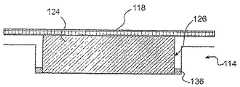
図2を参照すると、本発明により作られた全般的に符号114のサセプタの一実施形態が示されている。サセプタ114は、図1で示された処理チャンバなどの処理チャンバに配置されるように構成される。 Referring to FIG. 2, there is shown one embodiment of a generally 114 susceptor made in accordance with the present invention. The
図2に示されるように、サセプタ114は、半導体ウエハを加熱するための加熱デバイス116と協働して動作するように配置される。加熱デバイスは、無線周波数誘導コイルなどの任意の適切なヒータでありえる。代わりに、サセプタは、電気抵抗ヒータによって加熱されることができる。ある実施形態において、例えば、加熱デバイスは、炭化シリコンによって囲まれたグラファイト素子を含む誘導ヒータである。加熱デバイス116は、半導体ウエハを保持するように構成されたサセプタの一部に一体化されることができ、または代わりに、間隔を空けた関係でサセプタの表面を加熱することができる。 As shown in FIG. 2, the
図2に示されるように、サセプタ114は、半導体ウエハ118を受けるためのポケット120を含む。本発明によれば、ウエハ118は、支持構造体124上に配置される。支持構造体124は、少なくとも1つのリセス126内に配置される。示されるように、支持構造体124は、リセス126の底部内で固定される。しかしながら、一般に、リセス126の内側壁は、サセプタ114と支持構造体との間で直接の熱伝達を防止するために、支持構造体124と非接触の関係にある。 As shown in FIG. 2, the
支持構造体124の目的は、ポケット120の頂部表面上でウエハ118を懸架し、かつ有意な径方向の温度勾配がないように、より均一なウエハの加熱を支援することである。上述のように、特に低温壁処理チャンバにおいて、半導体ウエハ118は、放射によって、囲んでいるチャンバ壁に対して熱を失うことができる。ウエハを通る熱伝達のために、温度勾配は、ウエハの厚みを介して展開する。本発明のシステムおよびプロセスの目的は、径方向の温度勾配の展開または生成なしに、ウエハの厚みを介して熱伝達を可能にすることである。本発明により加熱されたウエハで展開する径方向の温度勾配の傾向は、支持構造体124の使用により低減される。一般に、支持構造体124は、加熱サイクルの間に実質的に同一の温度でウエハの底部表面を維持し、径方向の温度勾配の形成を防ぐ。 The purpose of the
サセプタ上のウエハ温度の均一性を促進するために、理想的には、支持構造体は、サセプタの表面とウエハの底部表面との間に存在する任意のガスと実質的に同一の伝導率を有する。しかしながら、あいにく、ガスの伝導率に等しい伝導率を有する固体材料は存在しない。固体材料の伝導率は常により高い。しかしながら、本発明によれば、サセプタを形成するために使用された材料の伝導率より著しく低い伝導率を有する、支持構造体の材料を使用することによって、かつ支持構造体に、サセプタに形成されるリセスにおける特定の高さを提供することによって、ウエハにおける温度均一性が維持されることが、本発明者によって見出された。 In order to promote uniformity of the wafer temperature on the susceptor, ideally, the support structure will have substantially the same conductivity as any gas present between the surface of the susceptor and the bottom surface of the wafer. Have. Unfortunately, however, no solid material has a conductivity equal to that of the gas. The conductivity of solid materials is always higher. However, according to the present invention, the susceptor is formed on the susceptor by using the material of the support structure and having a conductivity significantly lower than that of the material used to form the susceptor. It has been found by the present inventors that temperature uniformity in the wafer is maintained by providing a specific height in the recess.
例えば、サセプタおよび処理ガスを介する熱抵抗値に等しく、支持構造体を介する熱抵抗値を設定することによって、以下の式が得られる。
(Tg1−Tw)ks/ds=(1/(dr/Ksu+dg/kg))(Tg1−Tw)+σ*(1/(1/εs+1/εw−1))(Tg24−Tw4)
ここで、
ksは支持構造体の伝導率であり、
dsは支持構造体の高さであり、
ksuはサセプタの伝導率であり、
drはリセスの高さであり、
kgは処理ガスの伝導率であり、
dgはウエハとサセプタとの間の距離であり、
Tg1はリセスの底部のサセプタ温度であり、
Tg2はサセプタ頂部表面温度であり、
Twはウエハ底部表面温度であり、
σはStefan−Boltzmann定数であり、
εsはサセプタの放射率であり、
εwはウエハの放射率である。For example, by setting the thermal resistance value through the support structure equal to the thermal resistance value through the susceptor and the processing gas, the following equation is obtained.
(T g1 -T w) k s / d s = (1 / (d r / K su + d g / k g)) (T g1 -T w) + σ * (1 / (1 / ε s + 1 / ε w-1)) (T g2 4 -T w 4)
here,
ks is the conductivity of the support structure,
ds is the height of the support structure;
ksu is the conductivity of the susceptor,
dr is the height of the recess,
kg is the conductivity of the process gas,
dg is the distance between the wafer and the susceptor;
Tg1 is the susceptor temperature at the bottom of the recess,
Tg2 is the susceptor top surface temperature,
Tw is the wafer bottom surface temperature,
σ is a Stefan-Boltzmann constant,
εs is the emissivity of the susceptor,
εw is the emissivity of the wafer.
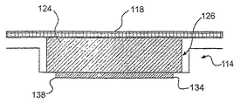
図3を参照すると、支持構造体124の拡大図に、サセプタ114上のウエハ118の支持が示されている。示されるように、支持構造体124は、リセス126内に配置される。支持構造体124は、リセスの内壁に接触することなくリセス126内に配置される。 Referring to FIG. 3, an enlarged view of the
図3は、上記式で使用される様々な距離およびパラメータを示す。上述のように、上記式は、支持構造体を介する熱束130は、サセプタを介し、かつサセプタとウエハとの間のギャップを介する熱束132に等しい状態を表すことを目的としている。図3において、処理ガス128は、ウエハとサセプタとの間の空間に存在する。 FIG. 3 shows the various distances and parameters used in the above equation. As described above, the above equation is intended to represent a state where the
本発明によれば、支持構造体124の伝導率が、サセプタ114の伝導率よりかなり小さく(ks<<ksu)、かつウエハとサセプタとの間の放射エネルギーが無視できるなら、上記式は以下のように単純化されることができる。In accordance with the present invention, if the conductivity of the
上記単純化は、サセプタが、グラファイトまたは炭化シリコンなどの高い熱伝導率を有する材料から作られるとき、特に適用可能である。上記に示されるように、この場合、支持構造体の高さは、支持構造体の伝導率と処理ガスの伝導率との比を掛けた、ウエハとサセプタとの間の距離に等しい。 The above simplification is particularly applicable when the susceptor is made from a material with high thermal conductivity, such as graphite or silicon carbide. As indicated above, in this case, the height of the support structure is equal to the distance between the wafer and the susceptor multiplied by the ratio of the conductivity of the support structure to the conductivity of the process gas.
本発明によりサセプタを構成するときに、上記計算された距離に可能な限り近い支持構造体の高さを有することが一般に望ましい。しかしながら、許容可能な結果は、支持構造体の高さが、上記計算された距離の約25%以内、特に上記計算された距離の約10%以内、より特に上記計算された距離の約5%以内であるなら達成される。 When constructing a susceptor according to the present invention, it is generally desirable to have the height of the support structure as close as possible to the calculated distance. However, acceptable results show that the height of the support structure is within about 25% of the calculated distance, particularly within about 10% of the calculated distance, more particularly about 5% of the calculated distance. Achieved if within.
本発明で使用される支持構造体124の実際の高さは、様々な要因に応じて変わる。そのような要因は、支持構造体を構成するために使用される材料、処理ガスの伝導率、ウエハとサセプタとの間の距離、処理温度などを含む。一般にある実施形態において、支持構造体124の高さは、約0.5mm(約0.02インチ)から約2.5mm(約0.1インチ)までであり、特に約約0.75mm(約0.03インチ)から約2mm(約0.08インチ)までであることができる。これらの高さで、リセス126の深さは、約0.25mm(約0.01インチ)から約2mm(約0.08インチ)まで、特に約0.5mm(約0.02インチ)から約1.25mm(0.05インチ)までであることができる。サセプタ内のリセスの存在は、特定の支持構造体の高さに関して許容し、一方、ウエハがまだ所望のサセプタの頂部表面に近いように維持する。 The actual height of the
例えば、加熱サイクルの間、ウエハ118は、サセプタの頂部表面から約0.025mm(約1mil)から約0.5mm(約20mil)、特に約0.125mm(約5mil)から約0.275mm(約11mil)から離間されるべきである。ある実施形態において、サセプタの表面は、ウエハを受けるためにポケット120を形成する。ある好ましい実施形態において、ポケットの頂部表面は、一般に最高処理温度でウエハの形状に一致する形状を有する。例えば最高処理温度で、ウエハが曲がる傾向があるなら、ポケット120の頂部表面は、ウエハにおける曲がりに一致すべきである。ウエハを通じてより良い温度均一性は、ウエハのサセプタとの接触なしに、サセプタとウエハとの均一な距離を維持することによって維持される。理想的には、最高処理温度で、ポケット120の頂部表面とウエハ118の底部表面との距離は、約0.05mm(約2mil)以下だけ、特に約0.025mm(約1mil)以下だけ変化すべきである。 For example, during a heating cycle, the
様々な材料が、本発明による支持構造体124を形成するために使用されることができることが考えられる。一般に、支持構造体を形成するために選択される材料は、より高い温度で比較的低い熱伝導率を有するべきであり、加熱されたとき処理チャンバを汚染すべきではない。例えば、支持構造体を形成するために使用される材料は、ウエハが加熱される温度で金属ガスを形成するべきではない。 It is contemplated that a variety of materials can be used to form the
一般に、支持構造体の熱伝導率は、約0.06cal/cm・s・℃より低いことができ、好ましくは、約1100℃以上で約0.0037cal/cm・s・℃から約0.06cal/cm・s・℃であることができる。本発明で使用するのに良く適した特定の材料は、水晶、サファイヤ、またはダイアモンドを含む。 In general, the thermal conductivity of the support structure can be less than about 0.06 cal / cm · s · ° C., preferably from about 0.0037 cal / cm · s · ° C. to about 0.06 cal above about 1100 ° C. / Cm · s · ° C. Specific materials well suited for use with the present invention include quartz, sapphire, or diamond.
本発明のシステムおよびプロセスを介して、ウエハを、有意な径方向の温度勾配なく、熱処理チャンバ内での加熱されたサセプタ上で非常に有効に加熱することができる。例えば、ウエハを、径方向に10℃以下の温度差を有し、特に約5℃以下の温度差を有し、ある実施形態において、径方向に約3℃以下の温度差を有するように、本発明により処理することができると考えられる。 Through the system and process of the present invention, the wafer can be heated very effectively on a heated susceptor in a thermal processing chamber without significant radial temperature gradients. For example, the wafer may have a temperature difference of 10 ° C. or less in the radial direction, particularly a temperature difference of about 5 ° C. or less, and in one embodiment, a temperature difference of about 3 ° C. or less in the radial direction, It is believed that it can be processed according to the present invention.
上述のように、支持構造体124は、一般にサセプタ114内に形成されたリセスに配置される。支持構造体124は、リセス内に配置されたときに、リセスの内壁から所定の距離だけ離間されるべきである。しかしながら支持構造体は、また、一旦リセス内に配置されると、所定の位置のままであるべきである。 As described above, the
図4Aから図4Cを参照すると、支持構造体およびリセス構造の様々な実施形態が示されている。 Referring to FIGS. 4A-4C, various embodiments of support structures and recess structures are shown.
例えば図4Aに示されるように、支持構造体124は、全般的に均一な幅または径を有する。しかしながら、リセス126は、窪んだ部分(indented portion)134を含む。この部分は、支持構造体を特定の位置に維持するように構成される。 For example, as shown in FIG. 4A, the
一方、図4Bに示される実施形態において、支持構造体124は、リセス内に整列された状態で支持構造体124を維持するためのフットまたはタブ部分136を含む。 On the other hand, in the embodiment shown in FIG. 4B, the
図4Cを参照すると、支持構造体およびリセス構造の他の実施形態が示されている。この実施形態において、リセス126は窪んだ部分134を含み、一方、支持構造体124は対応する狭い部分138を含む。狭い部分138は、窪んだ部分134内にぴったりと嵌まる。 Referring to FIG. 4C, another embodiment of a support structure and a recess structure is shown. In this embodiment, the
その高さを除いて、支持構造体のサイズおよび形状は、一般に上述の数式とは無関係である。したがって、支持構造体を、半導体ウエハを支持できる任意の適切な形状で提供することができる。例えば図5を参照すると、ある実施形態において、支持構造体124を、リングの形状にすることができる。リング124は、サセプタ114内に形成されたリセス126内に納めてもよい。この実施形態において、リセス126は、トレンチ状の形状を有することができる。 Except for its height, the size and shape of the support structure is generally independent of the above formula. Thus, the support structure can be provided in any suitable shape that can support the semiconductor wafer. For example, referring to FIG. 5, in one embodiment, the
ある実施形態において、支持構造体が、図5に示されるようなリングの形状であるときには、リングは、約6.25mm(約0.25インチ)の幅を有することができ、リセスは、約7.5mm(約0.3インチ)の幅を有するトレンチの形状であることができる。 In certain embodiments, when the support structure is in the shape of a ring as shown in FIG. 5, the ring can have a width of about 0.25 inches and the recess is about It can be in the form of a trench having a width of 7.5 mm (about 0.3 inches).
図5に示されるようなリング形状を有することに加えて、支持構造体は、図6および図7に示されるようなピン140の形状であることができる。示されるように、ピンは、半導体ウエハを均一に支持するために共通の径に沿って離間されることができる。一般に、3個以上のピンが、ウエハを支持するために必要である。 In addition to having a ring shape as shown in FIG. 5, the support structure can be in the shape of a
図6に示される実施形態において、ピン140は、その縁部でまたは縁部近くで半導体ウエハを支持するように配置される。しかしながら図7において、ピンは、その重心近くにウエハを支持するように配置される。しかしながら、支持構造体は、任意の適切なウエハ径に配置されることができることが理解されるべきである。 In the embodiment shown in FIG. 6, the
ピンの断面形状は、一般に重要ではない。例えば、図6において、ピンは円筒形状を有して示され、一方、図7において、ピンは正方形または矩形形状を有する。例示だけの目的のために、円筒形状であるときに、ピンは、約6.25mm(約0.25インチ)の直径を有することができ、約7.5mm(約0.3インチ)の直径を有するリセス内に配置されることができる。 The cross-sectional shape of the pin is generally not important. For example, in FIG. 6, the pin is shown having a cylindrical shape, while in FIG. 7, the pin has a square or rectangular shape. For purposes of illustration only, when cylindrical, the pin may have a diameter of about 0.25 inches and a diameter of about 7.5 inches. Can be placed in a recess.
ピン140の頂部表面は、ウエハを支持するための他の任意の形状であることができる。例えば、多くの適用のために、ピンの頂部表面は平坦であるべきである。 The top surface of the
本発明に対するこれらおよび他の修正形態および変形形態は、添付の特許請求の範囲により詳細に示される本発明の精神および範囲から逸脱することなく、当業者によって実施されることができる。さらに、様々な実施形態の態様は、全体または一部の両方で交換されることができる。さらに、前述の記載が例示だけを目的としており、添付の特許請求の範囲においてさらに記載されるように本発明を限定する目的ではないことは、当業者は理解するであろう。 These and other modifications and variations to the present invention may be practiced by those skilled in the art without departing from the spirit and scope of the invention as set forth in detail by the appended claims. Moreover, aspects of the various embodiments can be interchanged both in whole or in part. Moreover, those skilled in the art will appreciate that the foregoing description is for illustrative purposes only and is not intended to limit the invention as further described in the appended claims.
Claims (41)
Translated fromJapanese半導体ウエハを含むように構成された処理チャンバと、
前記処理チャンバ内に配置されるサセプタとを備え、前記サセプタが、半導体ウエハを受けるウエハ支持表面を備え、前記ウエハ支持表面が、少なくとも1つのリセスと前記リセス内に配置された対応する支持構造体とを含み、前記支持構造体が、前記ウエハの熱処理中に前記サセプタ上に半導体ウエハを上げるように構成され、前記支持構造体が、1100℃の温度で約0.06Cal/cm・s・℃以下の熱伝導率を有し、前記システムがさらに、
前記サセプタ上に支持された半導体ウエハを加熱するために、前記サセプタと協働して動作するように配置された加熱デバイスを備えることを特徴とするシステム。A system for processing a semiconductor substrate,
A processing chamber configured to contain a semiconductor wafer;
A susceptor disposed within the processing chamber, the susceptor comprising a wafer support surface for receiving a semiconductor wafer, the wafer support surface being disposed within the recess and the corresponding support structure. The support structure is configured to raise the semiconductor wafer onto the susceptor during the heat treatment of the wafer, and the support structure is about 0.06 Cal / cm · s · ° C. at a temperature of 1100 ° C. Having the following thermal conductivity, the system further comprising:
A system comprising: a heating device arranged to operate in cooperation with the susceptor to heat a semiconductor wafer supported on the susceptor.
ksは、前記支持構造体の熱伝導率であり、
kgは、前記処理チャンバ内に存在するガスの熱伝導率であることを特徴とする請求項1に記載のシステム。The support structure has a height that is within 5% of the distance calculated as follows:
ks is the thermal conductivity of the support structure;
The system of claim 1, wherein kg is a thermal conductivity of a gas present in the processing chamber.
加熱デバイスと、
半導体ウエハを受けるウエハ支持表面とを備え、前記ウエハ支持表面が、前記ウエハがポケットの頂部表面と接触することなく、加熱中に半導体ウエハが曲がることを許容するように構成された形状を有するポケットを画定し、前記サセプタがさらに、
前記ポケットの頂部表面上に半導体を懸架するための前記ウエハ支持表面から延びる支持構造体を備え、前記支持構造体が、1100℃の温度で約0.06Cal/cm・s・℃以下の熱伝導率を有する材料から作られることを特徴とするサセプタ。A susceptor for holding and heating a semiconductor wafer in a processing chamber,
A heating device;
A wafer support surface for receiving a semiconductor wafer, the wafer support surface having a shape configured to allow the semiconductor wafer to bend during heating without contacting the wafer with a top surface of the pocket. And the susceptor further comprises
A support structure extending from the wafer support surface for suspending a semiconductor on the top surface of the pocket, the support structure having a thermal conductivity of about 0.06 Cal / cm · s · ° C. or less at a temperature of 1100 ° C. Susceptor, characterized in that it is made from a material having a rate.
ksは、前記支持構造体の熱伝導率であり、
kgは、前記処理チャンバ内に存在するガスの熱伝導率であることを特徴とする請求項23に記載のサセプタ。The support structure has a height that is within 25% of the distance calculated as follows:
ks is the thermal conductivity of the support structure;
24. A susceptor according to claim 23, wherein kg is the thermal conductivity of the gas present in the processing chamber.
サセプタを含む処理チャンバを提供することを含み、前記サセプタは加熱されウエハ支持表面を画定し、前記サセプタが、さらにウエハ支持表面から延びる支持構造体を備え、前記ウエハ支持表面が、前記表面と接触することなく、加熱中に半導体ウエハが曲がることを許容するように構成された形状を有し、前記支持構造体が、1100℃で約0.06Cal/cm・s・℃以下の熱伝導率を有する材料から作られ、前記プロセスがさらに、
半導体ウエハを前記支持構造体に配置すること、および
前記ウエハ支持表面に接触することなく、前記ウエハを曲げさせる最高処理温度に前記半導体ウエハを加熱すること
を含むことを特徴とするプロセス。A process for uniformly heating a semiconductor wafer on a heated susceptor,
Providing a processing chamber including a susceptor, the susceptor being heated to define a wafer support surface, the susceptor further comprising a support structure extending from the wafer support surface, wherein the wafer support surface is in contact with the surface And the support structure has a thermal conductivity of about 0.06 Cal / cm · s · ° C. or less at 1100 ° C. having a shape configured to allow the semiconductor wafer to bend during heating. The process further comprising:
Placing the semiconductor wafer on the support structure; and heating the semiconductor wafer to a maximum processing temperature that causes the wafer to bend without contacting the wafer support surface.
ksは、前記支持構造体の熱伝導率であり、
kgは、前記処理チャンバ内に存在するガスの熱伝導率であることを特徴とする請求項29に記載のプロセス。The support structure has a height that is within 5% of the distance calculated at the maximum processing temperature as follows:
ks is the thermal conductivity of the support structure;
30. The process of claim 29, whereingg is the thermal conductivity of the gas present in the processing chamber.
Applications Claiming Priority (3)
| Application Number | Priority Date | Filing Date | Title |
|---|---|---|---|
| US10/141,515 | 2002-05-07 | ||
| US10/141,515US20030209326A1 (en) | 2002-05-07 | 2002-05-07 | Process and system for heating semiconductor substrates in a processing chamber containing a susceptor |
| PCT/US2003/011734WO2003096396A1 (en) | 2002-05-07 | 2003-04-15 | Process and system for heating semiconductor substrates in a processing chamber containing a susceptor |
Publications (2)
| Publication Number | Publication Date |
|---|---|
| JP2005530335Atrue JP2005530335A (en) | 2005-10-06 |
| JP4786177B2 JP4786177B2 (en) | 2011-10-05 |
Family
ID=29399681
Family Applications (1)
| Application Number | Title | Priority Date | Filing Date |
|---|---|---|---|
| JP2004504278AExpired - Fee RelatedJP4786177B2 (en) | 2002-05-07 | 2003-04-15 | Process and system for heating a semiconductor substrate in a processing chamber including a susceptor |
Country Status (8)
| Country | Link |
|---|---|
| US (2) | US20030209326A1 (en) |
| JP (1) | JP4786177B2 (en) |
| KR (1) | KR20040107477A (en) |
| CN (1) | CN100578734C (en) |
| AU (1) | AU2003221961A1 (en) |
| DE (1) | DE10392595T5 (en) |
| TW (1) | TWI278935B (en) |
| WO (1) | WO2003096396A1 (en) |
Cited By (3)
| Publication number | Priority date | Publication date | Assignee | Title |
|---|---|---|---|---|
| JP2013053355A (en)* | 2011-09-05 | 2013-03-21 | Taiyo Nippon Sanso Corp | Vapor phase deposition apparatus |
| KR20170076813A (en)* | 2009-12-02 | 2017-07-04 | 비코 인스트루먼츠 인코포레이티드 | Method for improving performance of a substrate carrier and a substrate carrier |
| JP2017539086A (en)* | 2014-11-28 | 2017-12-28 | アイクストロン、エスイー | Substrate holding device |
Families Citing this family (397)
| Publication number | Priority date | Publication date | Assignee | Title |
|---|---|---|---|---|
| WO2000031777A1 (en) | 1998-11-20 | 2000-06-02 | Steag Rtp Systems, Inc. | Fast heating and cooling apparatus for semiconductor wafers |
| US7015422B2 (en) | 2000-12-21 | 2006-03-21 | Mattson Technology, Inc. | System and process for heating semiconductor wafers by optimizing absorption of electromagnetic energy |
| US6970644B2 (en) | 2000-12-21 | 2005-11-29 | Mattson Technology, Inc. | Heating configuration for use in thermal processing chambers |
| US6902622B2 (en) | 2001-04-12 | 2005-06-07 | Mattson Technology, Inc. | Systems and methods for epitaxially depositing films on a semiconductor substrate |
| US7734439B2 (en)* | 2002-06-24 | 2010-06-08 | Mattson Technology, Inc. | System and process for calibrating pyrometers in thermal processing chambers |
| US7101812B2 (en) | 2002-09-20 | 2006-09-05 | Mattson Technology, Inc. | Method of forming and/or modifying a dielectric film on a semiconductor surface |
| US6835914B2 (en) | 2002-11-05 | 2004-12-28 | Mattson Technology, Inc. | Apparatus and method for reducing stray light in substrate processing chambers |
| DE10323085A1 (en)* | 2003-05-22 | 2004-12-09 | Aixtron Ag | CVD coater |
| US7654596B2 (en)* | 2003-06-27 | 2010-02-02 | Mattson Technology, Inc. | Endeffectors for handling semiconductor wafers |
| KR100527672B1 (en)* | 2003-07-25 | 2005-11-28 | 삼성전자주식회사 | Suscepter and apparatus for depositing included the same |
| US20050092439A1 (en)* | 2003-10-29 | 2005-05-05 | Keeton Tony J. | Low/high temperature substrate holder to reduce edge rolloff and backside damage |
| JP2007150132A (en)* | 2005-11-30 | 2007-06-14 | Toshiba Mitsubishi-Electric Industrial System Corp | Equalizer |
| JP5071703B2 (en)* | 2006-08-08 | 2012-11-14 | 独立行政法人物質・材料研究機構 | Semiconductor manufacturing equipment |
| KR100809335B1 (en) | 2006-09-28 | 2008-03-05 | 삼성전자주식회사 | Semiconductor device and manufacturing method thereof |
| US20080116521A1 (en) | 2006-11-16 | 2008-05-22 | Samsung Electronics Co., Ltd | CMOS Integrated Circuits that Utilize Insulating Layers with High Stress Characteristics to Improve NMOS and PMOS Transistor Carrier Mobilities and Methods of Forming Same |
| JP5117146B2 (en)* | 2006-12-15 | 2013-01-09 | 日本碍子株式会社 | Heating device |
| US7534678B2 (en) | 2007-03-27 | 2009-05-19 | Samsung Electronics Co., Ltd. | Methods of forming CMOS integrated circuit devices having stressed NMOS and PMOS channel regions therein and circuits formed thereby |
| JP5169097B2 (en) | 2007-09-14 | 2013-03-27 | 住友電気工業株式会社 | Semiconductor device manufacturing apparatus and manufacturing method |
| US7902082B2 (en) | 2007-09-20 | 2011-03-08 | Samsung Electronics Co., Ltd. | Method of forming field effect transistors using diluted hydrofluoric acid to remove sacrificial nitride spacers |
| US7923365B2 (en) | 2007-10-17 | 2011-04-12 | Samsung Electronics Co., Ltd. | Methods of forming field effect transistors having stress-inducing sidewall insulating spacers thereon |
| JP4924395B2 (en)* | 2007-12-07 | 2012-04-25 | 東京エレクトロン株式会社 | Processing apparatus and processing method |
| US7976216B2 (en) | 2007-12-20 | 2011-07-12 | Mattson Technology, Inc. | Determining the temperature of silicon at high temperatures |
| US10378106B2 (en) | 2008-11-14 | 2019-08-13 | Asm Ip Holding B.V. | Method of forming insulation film by modified PEALD |
| KR101612502B1 (en)* | 2008-12-18 | 2016-04-14 | 주성엔지니어링(주) | Method and apparatus for manufacturing semiconductor device |
| US9394608B2 (en) | 2009-04-06 | 2016-07-19 | Asm America, Inc. | Semiconductor processing reactor and components thereof |
| US8802201B2 (en) | 2009-08-14 | 2014-08-12 | Asm America, Inc. | Systems and methods for thin-film deposition of metal oxides using excited nitrogen-oxygen species |
| US9076827B2 (en) | 2010-09-14 | 2015-07-07 | Applied Materials, Inc. | Transfer chamber metrology for improved device yield |
| US20120234229A1 (en)* | 2011-03-16 | 2012-09-20 | Applied Materials, Inc. | Substrate support assembly for thin film deposition systems |
| US9312155B2 (en) | 2011-06-06 | 2016-04-12 | Asm Japan K.K. | High-throughput semiconductor-processing apparatus equipped with multiple dual-chamber modules |
| US10364496B2 (en) | 2011-06-27 | 2019-07-30 | Asm Ip Holding B.V. | Dual section module having shared and unshared mass flow controllers |
| US10854498B2 (en)* | 2011-07-15 | 2020-12-01 | Asm Ip Holding B.V. | Wafer-supporting device and method for producing same |
| US20130023129A1 (en) | 2011-07-20 | 2013-01-24 | Asm America, Inc. | Pressure transmitter for a semiconductor processing environment |
| US9017481B1 (en) | 2011-10-28 | 2015-04-28 | Asm America, Inc. | Process feed management for semiconductor substrate processing |
| CN102828238B (en)* | 2012-08-24 | 2015-11-04 | 东莞市中镓半导体科技有限公司 | Method for improving temperature field of substrate wafer surface in epitaxy process |
| US9659799B2 (en) | 2012-08-28 | 2017-05-23 | Asm Ip Holding B.V. | Systems and methods for dynamic semiconductor process scheduling |
| US9021985B2 (en) | 2012-09-12 | 2015-05-05 | Asm Ip Holdings B.V. | Process gas management for an inductively-coupled plasma deposition reactor |
| US10714315B2 (en) | 2012-10-12 | 2020-07-14 | Asm Ip Holdings B.V. | Semiconductor reaction chamber showerhead |
| US9583363B2 (en)* | 2012-12-31 | 2017-02-28 | Sunedison Semiconductor Limited (Uen201334164H) | Processes and apparatus for preparing heterostructures with reduced strain by radial distension |
| US20160376700A1 (en) | 2013-02-01 | 2016-12-29 | Asm Ip Holding B.V. | System for treatment of deposition reactor |
| US9484191B2 (en) | 2013-03-08 | 2016-11-01 | Asm Ip Holding B.V. | Pulsed remote plasma method and system |
| US9589770B2 (en) | 2013-03-08 | 2017-03-07 | Asm Ip Holding B.V. | Method and systems for in-situ formation of intermediate reactive species |
| US9240412B2 (en) | 2013-09-27 | 2016-01-19 | Asm Ip Holding B.V. | Semiconductor structure and device and methods of forming same using selective epitaxial process |
| US10683571B2 (en) | 2014-02-25 | 2020-06-16 | Asm Ip Holding B.V. | Gas supply manifold and method of supplying gases to chamber using same |
| US10167557B2 (en) | 2014-03-18 | 2019-01-01 | Asm Ip Holding B.V. | Gas distribution system, reactor including the system, and methods of using the same |
| US11015245B2 (en) | 2014-03-19 | 2021-05-25 | Asm Ip Holding B.V. | Gas-phase reactor and system having exhaust plenum and components thereof |
| KR102075994B1 (en) | 2014-03-25 | 2020-02-12 | 삼성전자주식회사 | Substrate separation device and substrate separation system |
| US10196741B2 (en)* | 2014-06-27 | 2019-02-05 | Applied Materials, Inc. | Wafer placement and gap control optimization through in situ feedback |
| CN106463453A (en)* | 2014-07-10 | 2017-02-22 | 应用材料公司 | Design of susceptor in chemical vapor deposition reactor |
| US10858737B2 (en) | 2014-07-28 | 2020-12-08 | Asm Ip Holding B.V. | Showerhead assembly and components thereof |
| US9890456B2 (en) | 2014-08-21 | 2018-02-13 | Asm Ip Holding B.V. | Method and system for in situ formation of gas-phase compounds |
| US10941490B2 (en) | 2014-10-07 | 2021-03-09 | Asm Ip Holding B.V. | Multiple temperature range susceptor, assembly, reactor and system including the susceptor, and methods of using the same |
| US9657845B2 (en) | 2014-10-07 | 2017-05-23 | Asm Ip Holding B.V. | Variable conductance gas distribution apparatus and method |
| KR102263121B1 (en) | 2014-12-22 | 2021-06-09 | 에이에스엠 아이피 홀딩 비.브이. | Semiconductor device and manufacuring method thereof |
| US10529542B2 (en) | 2015-03-11 | 2020-01-07 | Asm Ip Holdings B.V. | Cross-flow reactor and method |
| US10276355B2 (en) | 2015-03-12 | 2019-04-30 | Asm Ip Holding B.V. | Multi-zone reactor, system including the reactor, and method of using the same |
| US10458018B2 (en) | 2015-06-26 | 2019-10-29 | Asm Ip Holding B.V. | Structures including metal carbide material, devices including the structures, and methods of forming same |
| US10600673B2 (en) | 2015-07-07 | 2020-03-24 | Asm Ip Holding B.V. | Magnetic susceptor to baseplate seal |
| US10083836B2 (en) | 2015-07-24 | 2018-09-25 | Asm Ip Holding B.V. | Formation of boron-doped titanium metal films with high work function |
| KR102446726B1 (en) | 2015-09-11 | 2022-09-26 | 삼성전자주식회사 | Transparent plate and substrate processing apparatus including same |
| US9960072B2 (en) | 2015-09-29 | 2018-05-01 | Asm Ip Holding B.V. | Variable adjustment for precise matching of multiple chamber cavity housings |
| US10211308B2 (en) | 2015-10-21 | 2019-02-19 | Asm Ip Holding B.V. | NbMC layers |
| US10322384B2 (en) | 2015-11-09 | 2019-06-18 | Asm Ip Holding B.V. | Counter flow mixer for process chamber |
| CN106906516A (en)* | 2015-12-23 | 2017-06-30 | 财团法人工业技术研究院 | Nitride semiconductor substrate structure and carrier |
| US11139308B2 (en) | 2015-12-29 | 2021-10-05 | Asm Ip Holding B.V. | Atomic layer deposition of III-V compounds to form V-NAND devices |
| US10468251B2 (en) | 2016-02-19 | 2019-11-05 | Asm Ip Holding B.V. | Method for forming spacers using silicon nitride film for spacer-defined multiple patterning |
| US10529554B2 (en) | 2016-02-19 | 2020-01-07 | Asm Ip Holding B.V. | Method for forming silicon nitride film selectively on sidewalls or flat surfaces of trenches |
| DE102016103530A1 (en) | 2016-02-29 | 2017-08-31 | Aixtron Se | Substrate holding device with projecting from an annular groove supporting projections |
| US10501866B2 (en) | 2016-03-09 | 2019-12-10 | Asm Ip Holding B.V. | Gas distribution apparatus for improved film uniformity in an epitaxial system |
| US10343920B2 (en) | 2016-03-18 | 2019-07-09 | Asm Ip Holding B.V. | Aligned carbon nanotubes |
| US9892913B2 (en) | 2016-03-24 | 2018-02-13 | Asm Ip Holding B.V. | Radial and thickness control via biased multi-port injection settings |
| CN116200821A (en)* | 2016-03-28 | 2023-06-02 | 应用材料公司 | Base support |
| US10865475B2 (en) | 2016-04-21 | 2020-12-15 | Asm Ip Holding B.V. | Deposition of metal borides and silicides |
| US10190213B2 (en) | 2016-04-21 | 2019-01-29 | Asm Ip Holding B.V. | Deposition of metal borides |
| US10367080B2 (en) | 2016-05-02 | 2019-07-30 | Asm Ip Holding B.V. | Method of forming a germanium oxynitride film |
| US10032628B2 (en) | 2016-05-02 | 2018-07-24 | Asm Ip Holding B.V. | Source/drain performance through conformal solid state doping |
| KR102592471B1 (en) | 2016-05-17 | 2023-10-20 | 에이에스엠 아이피 홀딩 비.브이. | Method of forming metal interconnection and method of fabricating semiconductor device using the same |
| US11453943B2 (en) | 2016-05-25 | 2022-09-27 | Asm Ip Holding B.V. | Method for forming carbon-containing silicon/metal oxide or nitride film by ALD using silicon precursor and hydrocarbon precursor |
| US10388509B2 (en) | 2016-06-28 | 2019-08-20 | Asm Ip Holding B.V. | Formation of epitaxial layers via dislocation filtering |
| US9859151B1 (en) | 2016-07-08 | 2018-01-02 | Asm Ip Holding B.V. | Selective film deposition method to form air gaps |
| US10612137B2 (en) | 2016-07-08 | 2020-04-07 | Asm Ip Holdings B.V. | Organic reactants for atomic layer deposition |
| US10714385B2 (en) | 2016-07-19 | 2020-07-14 | Asm Ip Holding B.V. | Selective deposition of tungsten |
| KR102354490B1 (en) | 2016-07-27 | 2022-01-21 | 에이에스엠 아이피 홀딩 비.브이. | Method of processing a substrate |
| US9812320B1 (en) | 2016-07-28 | 2017-11-07 | Asm Ip Holding B.V. | Method and apparatus for filling a gap |
| KR102532607B1 (en) | 2016-07-28 | 2023-05-15 | 에이에스엠 아이피 홀딩 비.브이. | Substrate processing apparatus and method of operating the same |
| US10395919B2 (en) | 2016-07-28 | 2019-08-27 | Asm Ip Holding B.V. | Method and apparatus for filling a gap |
| US9887082B1 (en) | 2016-07-28 | 2018-02-06 | Asm Ip Holding B.V. | Method and apparatus for filling a gap |
| US10410943B2 (en) | 2016-10-13 | 2019-09-10 | Asm Ip Holding B.V. | Method for passivating a surface of a semiconductor and related systems |
| US10643826B2 (en) | 2016-10-26 | 2020-05-05 | Asm Ip Holdings B.V. | Methods for thermally calibrating reaction chambers |
| US11532757B2 (en) | 2016-10-27 | 2022-12-20 | Asm Ip Holding B.V. | Deposition of charge trapping layers |
| US10435790B2 (en) | 2016-11-01 | 2019-10-08 | Asm Ip Holding B.V. | Method of subatmospheric plasma-enhanced ALD using capacitively coupled electrodes with narrow gap |
| US10229833B2 (en) | 2016-11-01 | 2019-03-12 | Asm Ip Holding B.V. | Methods for forming a transition metal nitride film on a substrate by atomic layer deposition and related semiconductor device structures |
| US10714350B2 (en) | 2016-11-01 | 2020-07-14 | ASM IP Holdings, B.V. | Methods for forming a transition metal niobium nitride film on a substrate by atomic layer deposition and related semiconductor device structures |
| US10643904B2 (en) | 2016-11-01 | 2020-05-05 | Asm Ip Holdings B.V. | Methods for forming a semiconductor device and related semiconductor device structures |
| US10134757B2 (en) | 2016-11-07 | 2018-11-20 | Asm Ip Holding B.V. | Method of processing a substrate and a device manufactured by using the method |
| KR102546317B1 (en) | 2016-11-15 | 2023-06-21 | 에이에스엠 아이피 홀딩 비.브이. | Gas supply unit and substrate processing apparatus including the same |
| US10340135B2 (en) | 2016-11-28 | 2019-07-02 | Asm Ip Holding B.V. | Method of topologically restricted plasma-enhanced cyclic deposition of silicon or metal nitride |
| KR102762543B1 (en) | 2016-12-14 | 2025-02-05 | 에이에스엠 아이피 홀딩 비.브이. | Substrate processing apparatus |
| US11447861B2 (en) | 2016-12-15 | 2022-09-20 | Asm Ip Holding B.V. | Sequential infiltration synthesis apparatus and a method of forming a patterned structure |
| US11581186B2 (en) | 2016-12-15 | 2023-02-14 | Asm Ip Holding B.V. | Sequential infiltration synthesis apparatus |
| KR102700194B1 (en) | 2016-12-19 | 2024-08-28 | 에이에스엠 아이피 홀딩 비.브이. | Substrate processing apparatus |
| US10269558B2 (en) | 2016-12-22 | 2019-04-23 | Asm Ip Holding B.V. | Method of forming a structure on a substrate |
| US10867788B2 (en) | 2016-12-28 | 2020-12-15 | Asm Ip Holding B.V. | Method of forming a structure on a substrate |
| US11390950B2 (en) | 2017-01-10 | 2022-07-19 | Asm Ip Holding B.V. | Reactor system and method to reduce residue buildup during a film deposition process |
| US11979965B2 (en)* | 2017-01-10 | 2024-05-07 | King Abdullah University Of Science And Technology | Susceptors for induction heating with thermal uniformity |
| WO2018130953A1 (en)* | 2017-01-10 | 2018-07-19 | King Abdullah University Of Science And Technology | Susceptors for induction heating with thermal uniformity |
| US10655221B2 (en) | 2017-02-09 | 2020-05-19 | Asm Ip Holding B.V. | Method for depositing oxide film by thermal ALD and PEALD |
| US10468261B2 (en) | 2017-02-15 | 2019-11-05 | Asm Ip Holding B.V. | Methods for forming a metallic film on a substrate by cyclical deposition and related semiconductor device structures |
| US10529563B2 (en) | 2017-03-29 | 2020-01-07 | Asm Ip Holdings B.V. | Method for forming doped metal oxide films on a substrate by cyclical deposition and related semiconductor device structures |
| US10283353B2 (en) | 2017-03-29 | 2019-05-07 | Asm Ip Holding B.V. | Method of reforming insulating film deposited on substrate with recess pattern |
| KR102457289B1 (en) | 2017-04-25 | 2022-10-21 | 에이에스엠 아이피 홀딩 비.브이. | Method for depositing a thin film and manufacturing a semiconductor device |
| US10770286B2 (en) | 2017-05-08 | 2020-09-08 | Asm Ip Holdings B.V. | Methods for selectively forming a silicon nitride film on a substrate and related semiconductor device structures |
| US10446393B2 (en) | 2017-05-08 | 2019-10-15 | Asm Ip Holding B.V. | Methods for forming silicon-containing epitaxial layers and related semiconductor device structures |
| US10892156B2 (en) | 2017-05-08 | 2021-01-12 | Asm Ip Holding B.V. | Methods for forming a silicon nitride film on a substrate and related semiconductor device structures |
| US10504742B2 (en) | 2017-05-31 | 2019-12-10 | Asm Ip Holding B.V. | Method of atomic layer etching using hydrogen plasma |
| US10886123B2 (en) | 2017-06-02 | 2021-01-05 | Asm Ip Holding B.V. | Methods for forming low temperature semiconductor layers and related semiconductor device structures |
| US12040200B2 (en) | 2017-06-20 | 2024-07-16 | Asm Ip Holding B.V. | Semiconductor processing apparatus and methods for calibrating a semiconductor processing apparatus |
| US11306395B2 (en) | 2017-06-28 | 2022-04-19 | Asm Ip Holding B.V. | Methods for depositing a transition metal nitride film on a substrate by atomic layer deposition and related deposition apparatus |
| US10685834B2 (en) | 2017-07-05 | 2020-06-16 | Asm Ip Holdings B.V. | Methods for forming a silicon germanium tin layer and related semiconductor device structures |
| KR20190009245A (en) | 2017-07-18 | 2019-01-28 | 에이에스엠 아이피 홀딩 비.브이. | Methods for forming a semiconductor device structure and related semiconductor device structures |
| US11018002B2 (en) | 2017-07-19 | 2021-05-25 | Asm Ip Holding B.V. | Method for selectively depositing a Group IV semiconductor and related semiconductor device structures |
| US11374112B2 (en) | 2017-07-19 | 2022-06-28 | Asm Ip Holding B.V. | Method for depositing a group IV semiconductor and related semiconductor device structures |
| US10541333B2 (en) | 2017-07-19 | 2020-01-21 | Asm Ip Holding B.V. | Method for depositing a group IV semiconductor and related semiconductor device structures |
| US10605530B2 (en) | 2017-07-26 | 2020-03-31 | Asm Ip Holding B.V. | Assembly of a liner and a flange for a vertical furnace as well as the liner and the vertical furnace |
| US10312055B2 (en) | 2017-07-26 | 2019-06-04 | Asm Ip Holding B.V. | Method of depositing film by PEALD using negative bias |
| US10590535B2 (en) | 2017-07-26 | 2020-03-17 | Asm Ip Holdings B.V. | Chemical treatment, deposition and/or infiltration apparatus and method for using the same |
| TWI815813B (en) | 2017-08-04 | 2023-09-21 | 荷蘭商Asm智慧財產控股公司 | Showerhead assembly for distributing a gas within a reaction chamber |
| US10770336B2 (en) | 2017-08-08 | 2020-09-08 | Asm Ip Holding B.V. | Substrate lift mechanism and reactor including same |
| US10692741B2 (en) | 2017-08-08 | 2020-06-23 | Asm Ip Holdings B.V. | Radiation shield |
| US11769682B2 (en) | 2017-08-09 | 2023-09-26 | Asm Ip Holding B.V. | Storage apparatus for storing cassettes for substrates and processing apparatus equipped therewith |
| US10249524B2 (en) | 2017-08-09 | 2019-04-02 | Asm Ip Holding B.V. | Cassette holder assembly for a substrate cassette and holding member for use in such assembly |
| US11139191B2 (en) | 2017-08-09 | 2021-10-05 | Asm Ip Holding B.V. | Storage apparatus for storing cassettes for substrates and processing apparatus equipped therewith |
| US10236177B1 (en) | 2017-08-22 | 2019-03-19 | ASM IP Holding B.V.. | Methods for depositing a doped germanium tin semiconductor and related semiconductor device structures |
| USD900036S1 (en) | 2017-08-24 | 2020-10-27 | Asm Ip Holding B.V. | Heater electrical connector and adapter |
| US11830730B2 (en) | 2017-08-29 | 2023-11-28 | Asm Ip Holding B.V. | Layer forming method and apparatus |
| US11295980B2 (en) | 2017-08-30 | 2022-04-05 | Asm Ip Holding B.V. | Methods for depositing a molybdenum metal film over a dielectric surface of a substrate by a cyclical deposition process and related semiconductor device structures |
| US11056344B2 (en) | 2017-08-30 | 2021-07-06 | Asm Ip Holding B.V. | Layer forming method |
| KR102491945B1 (en) | 2017-08-30 | 2023-01-26 | 에이에스엠 아이피 홀딩 비.브이. | Substrate processing apparatus |
| KR102401446B1 (en) | 2017-08-31 | 2022-05-24 | 에이에스엠 아이피 홀딩 비.브이. | Substrate processing apparatus |
| US10607895B2 (en) | 2017-09-18 | 2020-03-31 | Asm Ip Holdings B.V. | Method for forming a semiconductor device structure comprising a gate fill metal |
| KR102630301B1 (en) | 2017-09-21 | 2024-01-29 | 에이에스엠 아이피 홀딩 비.브이. | Method of sequential infiltration synthesis treatment of infiltrateable material and structures and devices formed using same |
| US10844484B2 (en) | 2017-09-22 | 2020-11-24 | Asm Ip Holding B.V. | Apparatus for dispensing a vapor phase reactant to a reaction chamber and related methods |
| US10658205B2 (en) | 2017-09-28 | 2020-05-19 | Asm Ip Holdings B.V. | Chemical dispensing apparatus and methods for dispensing a chemical to a reaction chamber |
| US10403504B2 (en) | 2017-10-05 | 2019-09-03 | Asm Ip Holding B.V. | Method for selectively depositing a metallic film on a substrate |
| US10319588B2 (en) | 2017-10-10 | 2019-06-11 | Asm Ip Holding B.V. | Method for depositing a metal chalcogenide on a substrate by cyclical deposition |
| US10923344B2 (en) | 2017-10-30 | 2021-02-16 | Asm Ip Holding B.V. | Methods for forming a semiconductor structure and related semiconductor structures |
| KR102443047B1 (en) | 2017-11-16 | 2022-09-14 | 에이에스엠 아이피 홀딩 비.브이. | Method of processing a substrate and a device manufactured by the same |
| US10910262B2 (en) | 2017-11-16 | 2021-02-02 | Asm Ip Holding B.V. | Method of selectively depositing a capping layer structure on a semiconductor device structure |
| US11022879B2 (en) | 2017-11-24 | 2021-06-01 | Asm Ip Holding B.V. | Method of forming an enhanced unexposed photoresist layer |
| CN111344522B (en) | 2017-11-27 | 2022-04-12 | 阿斯莫Ip控股公司 | Including clean mini-environment device |
| WO2019103613A1 (en) | 2017-11-27 | 2019-05-31 | Asm Ip Holding B.V. | A storage device for storing wafer cassettes for use with a batch furnace |
| US10290508B1 (en) | 2017-12-05 | 2019-05-14 | Asm Ip Holding B.V. | Method for forming vertical spacers for spacer-defined patterning |
| US11574888B2 (en)* | 2017-12-15 | 2023-02-07 | Panasonic Intellectual Property Management Co., Ltd. | Component joining apparatus, component joining method and mounted structure |
| US10872771B2 (en) | 2018-01-16 | 2020-12-22 | Asm Ip Holding B. V. | Method for depositing a material film on a substrate within a reaction chamber by a cyclical deposition process and related device structures |
| KR102695659B1 (en) | 2018-01-19 | 2024-08-14 | 에이에스엠 아이피 홀딩 비.브이. | Method for depositing a gap filling layer by plasma assisted deposition |
| TWI799494B (en) | 2018-01-19 | 2023-04-21 | 荷蘭商Asm 智慧財產控股公司 | Deposition method |
| USD903477S1 (en) | 2018-01-24 | 2020-12-01 | Asm Ip Holdings B.V. | Metal clamp |
| US11018047B2 (en) | 2018-01-25 | 2021-05-25 | Asm Ip Holding B.V. | Hybrid lift pin |
| USD880437S1 (en) | 2018-02-01 | 2020-04-07 | Asm Ip Holding B.V. | Gas supply plate for semiconductor manufacturing apparatus |
| US10535516B2 (en) | 2018-02-01 | 2020-01-14 | Asm Ip Holdings B.V. | Method for depositing a semiconductor structure on a surface of a substrate and related semiconductor structures |
| US11081345B2 (en) | 2018-02-06 | 2021-08-03 | Asm Ip Holding B.V. | Method of post-deposition treatment for silicon oxide film |
| WO2019158960A1 (en) | 2018-02-14 | 2019-08-22 | Asm Ip Holding B.V. | A method for depositing a ruthenium-containing film on a substrate by a cyclical deposition process |
| US10896820B2 (en) | 2018-02-14 | 2021-01-19 | Asm Ip Holding B.V. | Method for depositing a ruthenium-containing film on a substrate by a cyclical deposition process |
| US10731249B2 (en) | 2018-02-15 | 2020-08-04 | Asm Ip Holding B.V. | Method of forming a transition metal containing film on a substrate by a cyclical deposition process, a method for supplying a transition metal halide compound to a reaction chamber, and related vapor deposition apparatus |
| US10658181B2 (en) | 2018-02-20 | 2020-05-19 | Asm Ip Holding B.V. | Method of spacer-defined direct patterning in semiconductor fabrication |
| KR102636427B1 (en) | 2018-02-20 | 2024-02-13 | 에이에스엠 아이피 홀딩 비.브이. | Substrate processing method and apparatus |
| US10975470B2 (en) | 2018-02-23 | 2021-04-13 | Asm Ip Holding B.V. | Apparatus for detecting or monitoring for a chemical precursor in a high temperature environment |
| US11473195B2 (en) | 2018-03-01 | 2022-10-18 | Asm Ip Holding B.V. | Semiconductor processing apparatus and a method for processing a substrate |
| US11629406B2 (en) | 2018-03-09 | 2023-04-18 | Asm Ip Holding B.V. | Semiconductor processing apparatus comprising one or more pyrometers for measuring a temperature of a substrate during transfer of the substrate |
| US11114283B2 (en) | 2018-03-16 | 2021-09-07 | Asm Ip Holding B.V. | Reactor, system including the reactor, and methods of manufacturing and using same |
| KR102646467B1 (en) | 2018-03-27 | 2024-03-11 | 에이에스엠 아이피 홀딩 비.브이. | Method of forming an electrode on a substrate and a semiconductor device structure including an electrode |
| US11230766B2 (en) | 2018-03-29 | 2022-01-25 | Asm Ip Holding B.V. | Substrate processing apparatus and method |
| US11088002B2 (en) | 2018-03-29 | 2021-08-10 | Asm Ip Holding B.V. | Substrate rack and a substrate processing system and method |
| US10510536B2 (en) | 2018-03-29 | 2019-12-17 | Asm Ip Holding B.V. | Method of depositing a co-doped polysilicon film on a surface of a substrate within a reaction chamber |
| KR102501472B1 (en) | 2018-03-30 | 2023-02-20 | 에이에스엠 아이피 홀딩 비.브이. | Substrate processing method |
| KR102600229B1 (en) | 2018-04-09 | 2023-11-10 | 에이에스엠 아이피 홀딩 비.브이. | Substrate supporting device, substrate processing apparatus including the same and substrate processing method |
| TWI811348B (en) | 2018-05-08 | 2023-08-11 | 荷蘭商Asm 智慧財產控股公司 | Methods for depositing an oxide film on a substrate by a cyclical deposition process and related device structures |
| US12025484B2 (en) | 2018-05-08 | 2024-07-02 | Asm Ip Holding B.V. | Thin film forming method |
| US12272527B2 (en) | 2018-05-09 | 2025-04-08 | Asm Ip Holding B.V. | Apparatus for use with hydrogen radicals and method of using same |
| KR20190129718A (en) | 2018-05-11 | 2019-11-20 | 에이에스엠 아이피 홀딩 비.브이. | Methods for forming a doped metal carbide film on a substrate and related semiconductor device structures |
| KR102596988B1 (en) | 2018-05-28 | 2023-10-31 | 에이에스엠 아이피 홀딩 비.브이. | Method of processing a substrate and a device manufactured by the same |
| TWI840362B (en) | 2018-06-04 | 2024-05-01 | 荷蘭商Asm Ip私人控股有限公司 | Wafer handling chamber with moisture reduction |
| US11718913B2 (en) | 2018-06-04 | 2023-08-08 | Asm Ip Holding B.V. | Gas distribution system and reactor system including same |
| US11286562B2 (en) | 2018-06-08 | 2022-03-29 | Asm Ip Holding B.V. | Gas-phase chemical reactor and method of using same |
| KR102568797B1 (en) | 2018-06-21 | 2023-08-21 | 에이에스엠 아이피 홀딩 비.브이. | Substrate processing system |
| US10797133B2 (en) | 2018-06-21 | 2020-10-06 | Asm Ip Holding B.V. | Method for depositing a phosphorus doped silicon arsenide film and related semiconductor device structures |
| TWI873894B (en) | 2018-06-27 | 2025-02-21 | 荷蘭商Asm Ip私人控股有限公司 | Cyclic deposition methods for forming metal-containing material and films and structures including the metal-containing material |
| KR102854019B1 (en) | 2018-06-27 | 2025-09-02 | 에이에스엠 아이피 홀딩 비.브이. | Periodic deposition method for forming a metal-containing material and films and structures comprising the metal-containing material |
| US10612136B2 (en) | 2018-06-29 | 2020-04-07 | ASM IP Holding, B.V. | Temperature-controlled flange and reactor system including same |
| KR102686758B1 (en) | 2018-06-29 | 2024-07-18 | 에이에스엠 아이피 홀딩 비.브이. | Method for depositing a thin film and manufacturing a semiconductor device |
| US10388513B1 (en) | 2018-07-03 | 2019-08-20 | Asm Ip Holding B.V. | Method for depositing silicon-free carbon-containing film as gap-fill layer by pulse plasma-assisted deposition |
| US10755922B2 (en) | 2018-07-03 | 2020-08-25 | Asm Ip Holding B.V. | Method for depositing silicon-free carbon-containing film as gap-fill layer by pulse plasma-assisted deposition |
| US10767789B2 (en) | 2018-07-16 | 2020-09-08 | Asm Ip Holding B.V. | Diaphragm valves, valve components, and methods for forming valve components |
| EP3597790A1 (en)* | 2018-07-19 | 2020-01-22 | King Abdullah University Of Science And Technology | Susceptors for induction heating with thermal uniformity |
| US10483099B1 (en) | 2018-07-26 | 2019-11-19 | Asm Ip Holding B.V. | Method for forming thermally stable organosilicon polymer film |
| US11053591B2 (en) | 2018-08-06 | 2021-07-06 | Asm Ip Holding B.V. | Multi-port gas injection system and reactor system including same |
| US10883175B2 (en) | 2018-08-09 | 2021-01-05 | Asm Ip Holding B.V. | Vertical furnace for processing substrates and a liner for use therein |
| US10829852B2 (en) | 2018-08-16 | 2020-11-10 | Asm Ip Holding B.V. | Gas distribution device for a wafer processing apparatus |
| US11430674B2 (en) | 2018-08-22 | 2022-08-30 | Asm Ip Holding B.V. | Sensor array, apparatus for dispensing a vapor phase reactant to a reaction chamber and related methods |
| US11024523B2 (en) | 2018-09-11 | 2021-06-01 | Asm Ip Holding B.V. | Substrate processing apparatus and method |
| KR102707956B1 (en) | 2018-09-11 | 2024-09-19 | 에이에스엠 아이피 홀딩 비.브이. | Method for deposition of a thin film |
| US11049751B2 (en) | 2018-09-14 | 2021-06-29 | Asm Ip Holding B.V. | Cassette supply system to store and handle cassettes and processing apparatus equipped therewith |
| CN110970344B (en) | 2018-10-01 | 2024-10-25 | Asmip控股有限公司 | Substrate holding apparatus, system comprising the same and method of using the same |
| US11232963B2 (en) | 2018-10-03 | 2022-01-25 | Asm Ip Holding B.V. | Substrate processing apparatus and method |
| KR102592699B1 (en) | 2018-10-08 | 2023-10-23 | 에이에스엠 아이피 홀딩 비.브이. | Substrate support unit and apparatuses for depositing thin film and processing the substrate including the same |
| US10847365B2 (en) | 2018-10-11 | 2020-11-24 | Asm Ip Holding B.V. | Method of forming conformal silicon carbide film by cyclic CVD |
| US10811256B2 (en) | 2018-10-16 | 2020-10-20 | Asm Ip Holding B.V. | Method for etching a carbon-containing feature |
| KR102605121B1 (en) | 2018-10-19 | 2023-11-23 | 에이에스엠 아이피 홀딩 비.브이. | Substrate processing apparatus and substrate processing method |
| KR102546322B1 (en) | 2018-10-19 | 2023-06-21 | 에이에스엠 아이피 홀딩 비.브이. | Substrate processing apparatus and substrate processing method |
| USD948463S1 (en) | 2018-10-24 | 2022-04-12 | Asm Ip Holding B.V. | Susceptor for semiconductor substrate supporting apparatus |
| US10381219B1 (en) | 2018-10-25 | 2019-08-13 | Asm Ip Holding B.V. | Methods for forming a silicon nitride film |
| US12378665B2 (en) | 2018-10-26 | 2025-08-05 | Asm Ip Holding B.V. | High temperature coatings for a preclean and etch apparatus and related methods |
| US11087997B2 (en) | 2018-10-31 | 2021-08-10 | Asm Ip Holding B.V. | Substrate processing apparatus for processing substrates |
| KR102748291B1 (en) | 2018-11-02 | 2024-12-31 | 에이에스엠 아이피 홀딩 비.브이. | Substrate support unit and substrate processing apparatus including the same |
| US11572620B2 (en) | 2018-11-06 | 2023-02-07 | Asm Ip Holding B.V. | Methods for selectively depositing an amorphous silicon film on a substrate |
| US11031242B2 (en) | 2018-11-07 | 2021-06-08 | Asm Ip Holding B.V. | Methods for depositing a boron doped silicon germanium film |
| US10818758B2 (en) | 2018-11-16 | 2020-10-27 | Asm Ip Holding B.V. | Methods for forming a metal silicate film on a substrate in a reaction chamber and related semiconductor device structures |
| US10847366B2 (en) | 2018-11-16 | 2020-11-24 | Asm Ip Holding B.V. | Methods for depositing a transition metal chalcogenide film on a substrate by a cyclical deposition process |
| US10559458B1 (en) | 2018-11-26 | 2020-02-11 | Asm Ip Holding B.V. | Method of forming oxynitride film |
| US12040199B2 (en) | 2018-11-28 | 2024-07-16 | Asm Ip Holding B.V. | Substrate processing apparatus for processing substrates |
| US11217444B2 (en) | 2018-11-30 | 2022-01-04 | Asm Ip Holding B.V. | Method for forming an ultraviolet radiation responsive metal oxide-containing film |
| KR102636428B1 (en) | 2018-12-04 | 2024-02-13 | 에이에스엠 아이피 홀딩 비.브이. | A method for cleaning a substrate processing apparatus |
| DE102018131987A1 (en) | 2018-12-12 | 2020-06-18 | Aixtron Se | Substrate holder for use in a CVD reactor |
| US11158513B2 (en) | 2018-12-13 | 2021-10-26 | Asm Ip Holding B.V. | Methods for forming a rhenium-containing film on a substrate by a cyclical deposition process and related semiconductor device structures |
| TWI874340B (en) | 2018-12-14 | 2025-03-01 | 荷蘭商Asm Ip私人控股有限公司 | Method of forming device structure, structure formed by the method and system for performing the method |
| TWI866480B (en) | 2019-01-17 | 2024-12-11 | 荷蘭商Asm Ip 私人控股有限公司 | Methods of forming a transition metal containing film on a substrate by a cyclical deposition process |
| KR102727227B1 (en) | 2019-01-22 | 2024-11-07 | 에이에스엠 아이피 홀딩 비.브이. | Semiconductor processing device |
| CN111524788B (en) | 2019-02-01 | 2023-11-24 | Asm Ip私人控股有限公司 | Method for forming topologically selective films of silicon oxide |
| TWI845607B (en) | 2019-02-20 | 2024-06-21 | 荷蘭商Asm Ip私人控股有限公司 | Cyclical deposition method and apparatus for filling a recess formed within a substrate surface |
| TWI873122B (en) | 2019-02-20 | 2025-02-21 | 荷蘭商Asm Ip私人控股有限公司 | Method of filling a recess formed within a surface of a substrate, semiconductor structure formed according to the method, and semiconductor processing apparatus |
| TWI838458B (en) | 2019-02-20 | 2024-04-11 | 荷蘭商Asm Ip私人控股有限公司 | Apparatus and methods for plug fill deposition in 3-d nand applications |
| KR102626263B1 (en) | 2019-02-20 | 2024-01-16 | 에이에스엠 아이피 홀딩 비.브이. | Cyclical deposition method including treatment step and apparatus for same |
| TWI842826B (en) | 2019-02-22 | 2024-05-21 | 荷蘭商Asm Ip私人控股有限公司 | Substrate processing apparatus and method for processing substrate |
| US11742198B2 (en) | 2019-03-08 | 2023-08-29 | Asm Ip Holding B.V. | Structure including SiOCN layer and method of forming same |
| KR102858005B1 (en) | 2019-03-08 | 2025-09-09 | 에이에스엠 아이피 홀딩 비.브이. | Method for Selective Deposition of Silicon Nitride Layer and Structure Including Selectively-Deposited Silicon Nitride Layer |
| KR102782593B1 (en) | 2019-03-08 | 2025-03-14 | 에이에스엠 아이피 홀딩 비.브이. | Structure Including SiOC Layer and Method of Forming Same |
| JP2020167398A (en) | 2019-03-28 | 2020-10-08 | エーエスエム・アイピー・ホールディング・ベー・フェー | Door openers and substrate processing equipment provided with door openers |
| KR102809999B1 (en) | 2019-04-01 | 2025-05-19 | 에이에스엠 아이피 홀딩 비.브이. | Method of manufacturing semiconductor device |
| KR20200123380A (en) | 2019-04-19 | 2020-10-29 | 에이에스엠 아이피 홀딩 비.브이. | Layer forming method and apparatus |
| KR20200125453A (en) | 2019-04-24 | 2020-11-04 | 에이에스엠 아이피 홀딩 비.브이. | Gas-phase reactor system and method of using same |
| KR20200130121A (en) | 2019-05-07 | 2020-11-18 | 에이에스엠 아이피 홀딩 비.브이. | Chemical source vessel with dip tube |
| US11289326B2 (en) | 2019-05-07 | 2022-03-29 | Asm Ip Holding B.V. | Method for reforming amorphous carbon polymer film |
| KR20200130652A (en) | 2019-05-10 | 2020-11-19 | 에이에스엠 아이피 홀딩 비.브이. | Method of depositing material onto a surface and structure formed according to the method |
| JP7612342B2 (en) | 2019-05-16 | 2025-01-14 | エーエスエム・アイピー・ホールディング・ベー・フェー | Wafer boat handling apparatus, vertical batch furnace and method |
| JP7598201B2 (en) | 2019-05-16 | 2024-12-11 | エーエスエム・アイピー・ホールディング・ベー・フェー | Wafer boat handling apparatus, vertical batch furnace and method |
| USD975665S1 (en) | 2019-05-17 | 2023-01-17 | Asm Ip Holding B.V. | Susceptor shaft |
| USD947913S1 (en) | 2019-05-17 | 2022-04-05 | Asm Ip Holding B.V. | Susceptor shaft |
| USD935572S1 (en) | 2019-05-24 | 2021-11-09 | Asm Ip Holding B.V. | Gas channel plate |
| USD922229S1 (en) | 2019-06-05 | 2021-06-15 | Asm Ip Holding B.V. | Device for controlling a temperature of a gas supply unit |
| KR20200141002A (en) | 2019-06-06 | 2020-12-17 | 에이에스엠 아이피 홀딩 비.브이. | Method of using a gas-phase reactor system including analyzing exhausted gas |
| KR20200141931A (en) | 2019-06-10 | 2020-12-21 | 에이에스엠 아이피 홀딩 비.브이. | Method for cleaning quartz epitaxial chambers |
| KR20200143254A (en) | 2019-06-11 | 2020-12-23 | 에이에스엠 아이피 홀딩 비.브이. | Method of forming an electronic structure using an reforming gas, system for performing the method, and structure formed using the method |
| USD944946S1 (en) | 2019-06-14 | 2022-03-01 | Asm Ip Holding B.V. | Shower plate |
| USD931978S1 (en) | 2019-06-27 | 2021-09-28 | Asm Ip Holding B.V. | Showerhead vacuum transport |
| KR20210005515A (en) | 2019-07-03 | 2021-01-14 | 에이에스엠 아이피 홀딩 비.브이. | Temperature control assembly for substrate processing apparatus and method of using same |
| JP7499079B2 (en) | 2019-07-09 | 2024-06-13 | エーエスエム・アイピー・ホールディング・ベー・フェー | Plasma device using coaxial waveguide and substrate processing method |
| CN112216646A (en) | 2019-07-10 | 2021-01-12 | Asm Ip私人控股有限公司 | Substrate supporting assembly and substrate processing device comprising same |
| KR20210010307A (en) | 2019-07-16 | 2021-01-27 | 에이에스엠 아이피 홀딩 비.브이. | Substrate processing apparatus |
| KR102860110B1 (en) | 2019-07-17 | 2025-09-16 | 에이에스엠 아이피 홀딩 비.브이. | Methods of forming silicon germanium structures |
| KR20210010816A (en) | 2019-07-17 | 2021-01-28 | 에이에스엠 아이피 홀딩 비.브이. | Radical assist ignition plasma system and method |
| US11643724B2 (en) | 2019-07-18 | 2023-05-09 | Asm Ip Holding B.V. | Method of forming structures using a neutral beam |
| KR20210010817A (en) | 2019-07-19 | 2021-01-28 | 에이에스엠 아이피 홀딩 비.브이. | Method of Forming Topology-Controlled Amorphous Carbon Polymer Film |
| TWI839544B (en) | 2019-07-19 | 2024-04-21 | 荷蘭商Asm Ip私人控股有限公司 | Method of forming topology-controlled amorphous carbon polymer film |
| TWI851767B (en) | 2019-07-29 | 2024-08-11 | 荷蘭商Asm Ip私人控股有限公司 | Methods for selective deposition utilizing n-type dopants and/or alternative dopants to achieve high dopant incorporation |
| US12169361B2 (en) | 2019-07-30 | 2024-12-17 | Asm Ip Holding B.V. | Substrate processing apparatus and method |
| CN112309899A (en) | 2019-07-30 | 2021-02-02 | Asm Ip私人控股有限公司 | Substrate processing apparatus |
| CN112309900A (en) | 2019-07-30 | 2021-02-02 | Asm Ip私人控股有限公司 | Substrate processing apparatus |
| US11587815B2 (en) | 2019-07-31 | 2023-02-21 | Asm Ip Holding B.V. | Vertical batch furnace assembly |
| US11227782B2 (en) | 2019-07-31 | 2022-01-18 | Asm Ip Holding B.V. | Vertical batch furnace assembly |
| US11587814B2 (en) | 2019-07-31 | 2023-02-21 | Asm Ip Holding B.V. | Vertical batch furnace assembly |
| CN112323048B (en) | 2019-08-05 | 2024-02-09 | Asm Ip私人控股有限公司 | Liquid level sensor for chemical source container |
| CN112342526A (en) | 2019-08-09 | 2021-02-09 | Asm Ip私人控股有限公司 | Heater assembly including cooling device and method of using same |
| USD965044S1 (en) | 2019-08-19 | 2022-09-27 | Asm Ip Holding B.V. | Susceptor shaft |
| USD965524S1 (en) | 2019-08-19 | 2022-10-04 | Asm Ip Holding B.V. | Susceptor support |
| JP2021031769A (en) | 2019-08-21 | 2021-03-01 | エーエスエム アイピー ホールディング ビー.ブイ. | Production apparatus of mixed gas of film deposition raw material and film deposition apparatus |
| USD940837S1 (en) | 2019-08-22 | 2022-01-11 | Asm Ip Holding B.V. | Electrode |
| KR20210024423A (en) | 2019-08-22 | 2021-03-05 | 에이에스엠 아이피 홀딩 비.브이. | Method for forming a structure with a hole |
| USD979506S1 (en) | 2019-08-22 | 2023-02-28 | Asm Ip Holding B.V. | Insulator |
| USD930782S1 (en) | 2019-08-22 | 2021-09-14 | Asm Ip Holding B.V. | Gas distributor |
| USD949319S1 (en) | 2019-08-22 | 2022-04-19 | Asm Ip Holding B.V. | Exhaust duct |
| KR20210024420A (en) | 2019-08-23 | 2021-03-05 | 에이에스엠 아이피 홀딩 비.브이. | Method for depositing silicon oxide film having improved quality by peald using bis(diethylamino)silane |
| US11286558B2 (en) | 2019-08-23 | 2022-03-29 | Asm Ip Holding B.V. | Methods for depositing a molybdenum nitride film on a surface of a substrate by a cyclical deposition process and related semiconductor device structures including a molybdenum nitride film |
| KR102806450B1 (en) | 2019-09-04 | 2025-05-12 | 에이에스엠 아이피 홀딩 비.브이. | Methods for selective deposition using a sacrificial capping layer |
| KR102733104B1 (en) | 2019-09-05 | 2024-11-22 | 에이에스엠 아이피 홀딩 비.브이. | Substrate processing apparatus |
| US11562901B2 (en) | 2019-09-25 | 2023-01-24 | Asm Ip Holding B.V. | Substrate processing method |
| CN112593212B (en) | 2019-10-02 | 2023-12-22 | Asm Ip私人控股有限公司 | Method for forming topologically selective silicon oxide film by cyclic plasma enhanced deposition process |
| KR20210042810A (en) | 2019-10-08 | 2021-04-20 | 에이에스엠 아이피 홀딩 비.브이. | Reactor system including a gas distribution assembly for use with activated species and method of using same |
| TWI846953B (en) | 2019-10-08 | 2024-07-01 | 荷蘭商Asm Ip私人控股有限公司 | Substrate processing device |
| TW202128273A (en) | 2019-10-08 | 2021-08-01 | 荷蘭商Asm Ip私人控股有限公司 | Gas injection system, reactor system, and method of depositing material on surface of substratewithin reaction chamber |
| TWI846966B (en) | 2019-10-10 | 2024-07-01 | 荷蘭商Asm Ip私人控股有限公司 | Method of forming a photoresist underlayer and structure including same |
| US12009241B2 (en) | 2019-10-14 | 2024-06-11 | Asm Ip Holding B.V. | Vertical batch furnace assembly with detector to detect cassette |
| TWI834919B (en) | 2019-10-16 | 2024-03-11 | 荷蘭商Asm Ip私人控股有限公司 | Method of topology-selective film formation of silicon oxide |
| US11637014B2 (en) | 2019-10-17 | 2023-04-25 | Asm Ip Holding B.V. | Methods for selective deposition of doped semiconductor material |
| KR102845724B1 (en) | 2019-10-21 | 2025-08-13 | 에이에스엠 아이피 홀딩 비.브이. | Apparatus and methods for selectively etching films |
| KR20210050453A (en) | 2019-10-25 | 2021-05-07 | 에이에스엠 아이피 홀딩 비.브이. | Methods for filling a gap feature on a substrate surface and related semiconductor structures |
| US11646205B2 (en) | 2019-10-29 | 2023-05-09 | Asm Ip Holding B.V. | Methods of selectively forming n-type doped material on a surface, systems for selectively forming n-type doped material, and structures formed using same |
| KR20210054983A (en) | 2019-11-05 | 2021-05-14 | 에이에스엠 아이피 홀딩 비.브이. | Structures with doped semiconductor layers and methods and systems for forming same |
| US11501968B2 (en) | 2019-11-15 | 2022-11-15 | Asm Ip Holding B.V. | Method for providing a semiconductor device with silicon filled gaps |
| KR102861314B1 (en) | 2019-11-20 | 2025-09-17 | 에이에스엠 아이피 홀딩 비.브이. | Method of depositing carbon-containing material on a surface of a substrate, structure formed using the method, and system for forming the structure |
| US11450529B2 (en) | 2019-11-26 | 2022-09-20 | Asm Ip Holding B.V. | Methods for selectively forming a target film on a substrate comprising a first dielectric surface and a second metallic surface |
| CN112951697B (en) | 2019-11-26 | 2025-07-29 | Asmip私人控股有限公司 | Substrate processing apparatus |
| CN120432376A (en) | 2019-11-29 | 2025-08-05 | Asm Ip私人控股有限公司 | Substrate processing apparatus |
| CN112885692B (en) | 2019-11-29 | 2025-08-15 | Asmip私人控股有限公司 | Substrate processing apparatus |
| JP7527928B2 (en) | 2019-12-02 | 2024-08-05 | エーエスエム・アイピー・ホールディング・ベー・フェー | Substrate processing apparatus and substrate processing method |
| KR20210070898A (en) | 2019-12-04 | 2021-06-15 | 에이에스엠 아이피 홀딩 비.브이. | Substrate processing apparatus |
| KR20210078405A (en) | 2019-12-17 | 2021-06-28 | 에이에스엠 아이피 홀딩 비.브이. | Method of forming vanadium nitride layer and structure including the vanadium nitride layer |
| KR20210080214A (en) | 2019-12-19 | 2021-06-30 | 에이에스엠 아이피 홀딩 비.브이. | Methods for filling a gap feature on a substrate and related semiconductor structures |
| JP7636892B2 (en) | 2020-01-06 | 2025-02-27 | エーエスエム・アイピー・ホールディング・ベー・フェー | Channeled Lift Pins |
| JP7730637B2 (en) | 2020-01-06 | 2025-08-28 | エーエスエム・アイピー・ホールディング・ベー・フェー | Gas delivery assembly, components thereof, and reactor system including same |
| US11993847B2 (en) | 2020-01-08 | 2024-05-28 | Asm Ip Holding B.V. | Injector |
| KR20210093163A (en) | 2020-01-16 | 2021-07-27 | 에이에스엠 아이피 홀딩 비.브이. | Method of forming high aspect ratio features |
| KR102675856B1 (en) | 2020-01-20 | 2024-06-17 | 에이에스엠 아이피 홀딩 비.브이. | Method of forming thin film and method of modifying surface of thin film |
| TWI889744B (en) | 2020-01-29 | 2025-07-11 | 荷蘭商Asm Ip私人控股有限公司 | Contaminant trap system, and baffle plate stack |
| TW202513845A (en) | 2020-02-03 | 2025-04-01 | 荷蘭商Asm Ip私人控股有限公司 | Semiconductor structures and methods for forming the same |
| KR20210100010A (en) | 2020-02-04 | 2021-08-13 | 에이에스엠 아이피 홀딩 비.브이. | Method and apparatus for transmittance measurements of large articles |
| US11776846B2 (en) | 2020-02-07 | 2023-10-03 | Asm Ip Holding B.V. | Methods for depositing gap filling fluids and related systems and devices |
| KR20210103956A (en) | 2020-02-13 | 2021-08-24 | 에이에스엠 아이피 홀딩 비.브이. | Substrate processing apparatus including light receiving device and calibration method of light receiving device |
| TW202146691A (en) | 2020-02-13 | 2021-12-16 | 荷蘭商Asm Ip私人控股有限公司 | Gas distribution assembly, shower plate assembly, and method of adjusting conductance of gas to reaction chamber |
| TWI855223B (en) | 2020-02-17 | 2024-09-11 | 荷蘭商Asm Ip私人控股有限公司 | Method for growing phosphorous-doped silicon layer |
| CN113410160A (en) | 2020-02-28 | 2021-09-17 | Asm Ip私人控股有限公司 | System specially used for cleaning parts |
| KR20210113043A (en) | 2020-03-04 | 2021-09-15 | 에이에스엠 아이피 홀딩 비.브이. | Alignment fixture for a reactor system |
| KR20210116240A (en) | 2020-03-11 | 2021-09-27 | 에이에스엠 아이피 홀딩 비.브이. | Substrate handling device with adjustable joints |
| US11876356B2 (en) | 2020-03-11 | 2024-01-16 | Asm Ip Holding B.V. | Lockout tagout assembly and system and method of using same |
| KR102775390B1 (en) | 2020-03-12 | 2025-02-28 | 에이에스엠 아이피 홀딩 비.브이. | Method for Fabricating Layer Structure Having Target Topological Profile |
| US12173404B2 (en) | 2020-03-17 | 2024-12-24 | Asm Ip Holding B.V. | Method of depositing epitaxial material, structure formed using the method, and system for performing the method |
| KR102755229B1 (en) | 2020-04-02 | 2025-01-14 | 에이에스엠 아이피 홀딩 비.브이. | Thin film forming method |
| TWI887376B (en) | 2020-04-03 | 2025-06-21 | 荷蘭商Asm Ip私人控股有限公司 | Method for manufacturing semiconductor device |
| TWI888525B (en) | 2020-04-08 | 2025-07-01 | 荷蘭商Asm Ip私人控股有限公司 | Apparatus and methods for selectively etching silcon oxide films |
| KR20210128343A (en) | 2020-04-15 | 2021-10-26 | 에이에스엠 아이피 홀딩 비.브이. | Method of forming chromium nitride layer and structure including the chromium nitride layer |
| US11821078B2 (en) | 2020-04-15 | 2023-11-21 | Asm Ip Holding B.V. | Method for forming precoat film and method for forming silicon-containing film |
| US11996289B2 (en) | 2020-04-16 | 2024-05-28 | Asm Ip Holding B.V. | Methods of forming structures including silicon germanium and silicon layers, devices formed using the methods, and systems for performing the methods |
| KR20210130646A (en) | 2020-04-21 | 2021-11-01 | 에이에스엠 아이피 홀딩 비.브이. | Method for processing a substrate |
| KR20210132612A (en) | 2020-04-24 | 2021-11-04 | 에이에스엠 아이피 홀딩 비.브이. | Methods and apparatus for stabilizing vanadium compounds |
| TW202208671A (en) | 2020-04-24 | 2022-03-01 | 荷蘭商Asm Ip私人控股有限公司 | Methods of forming structures including vanadium boride and vanadium phosphide layers |
| KR20210132600A (en) | 2020-04-24 | 2021-11-04 | 에이에스엠 아이피 홀딩 비.브이. | Methods and systems for depositing a layer comprising vanadium, nitrogen, and a further element |
| KR102866804B1 (en) | 2020-04-24 | 2025-09-30 | 에이에스엠 아이피 홀딩 비.브이. | Vertical batch furnace assembly comprising a cooling gas supply |
| CN113555279A (en) | 2020-04-24 | 2021-10-26 | Asm Ip私人控股有限公司 | Methods of forming vanadium nitride-containing layers and structures comprising the same |
| KR102783898B1 (en) | 2020-04-29 | 2025-03-18 | 에이에스엠 아이피 홀딩 비.브이. | Solid source precursor vessel |
| KR20210134869A (en) | 2020-05-01 | 2021-11-11 | 에이에스엠 아이피 홀딩 비.브이. | Fast FOUP swapping with a FOUP handler |
| JP7726664B2 (en) | 2020-05-04 | 2025-08-20 | エーエスエム・アイピー・ホールディング・ベー・フェー | Substrate processing system for processing a substrate |
| KR102788543B1 (en) | 2020-05-13 | 2025-03-27 | 에이에스엠 아이피 홀딩 비.브이. | Laser alignment fixture for a reactor system |
| TW202146699A (en) | 2020-05-15 | 2021-12-16 | 荷蘭商Asm Ip私人控股有限公司 | Method of forming a silicon germanium layer, semiconductor structure, semiconductor device, method of forming a deposition layer, and deposition system |
| KR20210143653A (en) | 2020-05-19 | 2021-11-29 | 에이에스엠 아이피 홀딩 비.브이. | Substrate processing apparatus |
| KR20210145079A (en) | 2020-05-21 | 2021-12-01 | 에이에스엠 아이피 홀딩 비.브이. | Flange and apparatus for processing substrates |
| KR102795476B1 (en) | 2020-05-21 | 2025-04-11 | 에이에스엠 아이피 홀딩 비.브이. | Structures including multiple carbon layers and methods of forming and using same |
| TWI873343B (en) | 2020-05-22 | 2025-02-21 | 荷蘭商Asm Ip私人控股有限公司 | Reaction system for forming thin film on substrate |
| KR20210146802A (en) | 2020-05-26 | 2021-12-06 | 에이에스엠 아이피 홀딩 비.브이. | Method for depositing boron and gallium containing silicon germanium layers |
| TWI876048B (en) | 2020-05-29 | 2025-03-11 | 荷蘭商Asm Ip私人控股有限公司 | Substrate processing device |
| TW202212620A (en) | 2020-06-02 | 2022-04-01 | 荷蘭商Asm Ip私人控股有限公司 | Apparatus for processing substrate, method of forming film, and method of controlling apparatus for processing substrate |
| TW202208659A (en) | 2020-06-16 | 2022-03-01 | 荷蘭商Asm Ip私人控股有限公司 | Method for depositing boron containing silicon germanium layers |
| TW202218133A (en) | 2020-06-24 | 2022-05-01 | 荷蘭商Asm Ip私人控股有限公司 | Method for forming a layer provided with silicon |
| TWI873359B (en) | 2020-06-30 | 2025-02-21 | 荷蘭商Asm Ip私人控股有限公司 | Substrate processing method |
| US12431354B2 (en) | 2020-07-01 | 2025-09-30 | Asm Ip Holding B.V. | Silicon nitride and silicon oxide deposition methods using fluorine inhibitor |
| TW202202649A (en) | 2020-07-08 | 2022-01-16 | 荷蘭商Asm Ip私人控股有限公司 | Substrate processing method |
| KR20220010438A (en) | 2020-07-17 | 2022-01-25 | 에이에스엠 아이피 홀딩 비.브이. | Structures and methods for use in photolithography |
| TWI878570B (en) | 2020-07-20 | 2025-04-01 | 荷蘭商Asm Ip私人控股有限公司 | Method and system for depositing molybdenum layers |
| KR20220011092A (en) | 2020-07-20 | 2022-01-27 | 에이에스엠 아이피 홀딩 비.브이. | Method and system for forming structures including transition metal layers |
| US12322591B2 (en) | 2020-07-27 | 2025-06-03 | Asm Ip Holding B.V. | Thin film deposition process |
| KR20220021863A (en) | 2020-08-14 | 2022-02-22 | 에이에스엠 아이피 홀딩 비.브이. | Method for processing a substrate |
| US12040177B2 (en) | 2020-08-18 | 2024-07-16 | Asm Ip Holding B.V. | Methods for forming a laminate film by cyclical plasma-enhanced deposition processes |
| TW202228863A (en) | 2020-08-25 | 2022-08-01 | 荷蘭商Asm Ip私人控股有限公司 | Method for cleaning a substrate, method for selectively depositing, and reaction system |
| US11725280B2 (en) | 2020-08-26 | 2023-08-15 | Asm Ip Holding B.V. | Method for forming metal silicon oxide and metal silicon oxynitride layers |
| TW202229601A (en) | 2020-08-27 | 2022-08-01 | 荷蘭商Asm Ip私人控股有限公司 | Method of forming patterned structures, method of manipulating mechanical property, device structure, and substrate processing system |
| TW202217045A (en) | 2020-09-10 | 2022-05-01 | 荷蘭商Asm Ip私人控股有限公司 | Methods for depositing gap filing fluids and related systems and devices |
| USD990534S1 (en) | 2020-09-11 | 2023-06-27 | Asm Ip Holding B.V. | Weighted lift pin |
| KR20220036866A (en) | 2020-09-16 | 2022-03-23 | 에이에스엠 아이피 홀딩 비.브이. | Silicon oxide deposition method |
| JP7361005B2 (en)* | 2020-09-18 | 2023-10-13 | 株式会社Kokusai Electric | Substrate processing equipment, substrate holder, semiconductor device manufacturing method, and program |
| USD1012873S1 (en) | 2020-09-24 | 2024-01-30 | Asm Ip Holding B.V. | Electrode for semiconductor processing apparatus |
| TWI889903B (en) | 2020-09-25 | 2025-07-11 | 荷蘭商Asm Ip私人控股有限公司 | Semiconductor processing method |
| US12009224B2 (en) | 2020-09-29 | 2024-06-11 | Asm Ip Holding B.V. | Apparatus and method for etching metal nitrides |
| KR20220045900A (en) | 2020-10-06 | 2022-04-13 | 에이에스엠 아이피 홀딩 비.브이. | Deposition method and an apparatus for depositing a silicon-containing material |
| CN114293174A (en) | 2020-10-07 | 2022-04-08 | Asm Ip私人控股有限公司 | Gas supply unit and substrate processing apparatus including the same |
| TW202229613A (en) | 2020-10-14 | 2022-08-01 | 荷蘭商Asm Ip私人控股有限公司 | Method of depositing material on stepped structure |
| TW202232565A (en) | 2020-10-15 | 2022-08-16 | 荷蘭商Asm Ip私人控股有限公司 | Method of manufacturing semiconductor device, and substrate treatment apparatus using ether-cat |
| TW202217037A (en) | 2020-10-22 | 2022-05-01 | 荷蘭商Asm Ip私人控股有限公司 | Method of depositing vanadium metal, structure, device and a deposition assembly |
| TW202223136A (en) | 2020-10-28 | 2022-06-16 | 荷蘭商Asm Ip私人控股有限公司 | Method for forming layer on substrate, and semiconductor processing system |
| TW202229620A (en) | 2020-11-12 | 2022-08-01 | 特文特大學 | Deposition system, method for controlling reaction condition, method for depositing |
| TW202229795A (en) | 2020-11-23 | 2022-08-01 | 荷蘭商Asm Ip私人控股有限公司 | A substrate processing apparatus with an injector |
| TW202235649A (en) | 2020-11-24 | 2022-09-16 | 荷蘭商Asm Ip私人控股有限公司 | Methods for filling a gap and related systems and devices |
| TW202235675A (en) | 2020-11-30 | 2022-09-16 | 荷蘭商Asm Ip私人控股有限公司 | Injector, and substrate processing apparatus |
| US12255053B2 (en) | 2020-12-10 | 2025-03-18 | Asm Ip Holding B.V. | Methods and systems for depositing a layer |
| TW202233884A (en) | 2020-12-14 | 2022-09-01 | 荷蘭商Asm Ip私人控股有限公司 | Method of forming structures for threshold voltage control |
| US11946137B2 (en) | 2020-12-16 | 2024-04-02 | Asm Ip Holding B.V. | Runout and wobble measurement fixtures |
| TW202232639A (en) | 2020-12-18 | 2022-08-16 | 荷蘭商Asm Ip私人控股有限公司 | Wafer processing apparatus with a rotatable table |
| TW202242184A (en) | 2020-12-22 | 2022-11-01 | 荷蘭商Asm Ip私人控股有限公司 | Precursor capsule, precursor vessel, vapor deposition assembly, and method of loading solid precursor into precursor vessel |
| TW202231903A (en) | 2020-12-22 | 2022-08-16 | 荷蘭商Asm Ip私人控股有限公司 | Transition metal deposition method, transition metal layer, and deposition assembly for depositing transition metal on substrate |
| TW202226899A (en) | 2020-12-22 | 2022-07-01 | 荷蘭商Asm Ip私人控股有限公司 | Plasma treatment device having matching box |
| US12170213B2 (en)* | 2021-02-17 | 2024-12-17 | Applied Materials, Inc. | Flat pocket susceptor design with improved heat transfer |
| TWI751078B (en)* | 2021-04-28 | 2021-12-21 | 錼創顯示科技股份有限公司 | Semiconductor wafer carrier structure and metal organic chemical vapor deposition device |
| USD1023959S1 (en) | 2021-05-11 | 2024-04-23 | Asm Ip Holding B.V. | Electrode for substrate processing apparatus |
| USD981973S1 (en) | 2021-05-11 | 2023-03-28 | Asm Ip Holding B.V. | Reactor wall for substrate processing apparatus |
| USD980814S1 (en) | 2021-05-11 | 2023-03-14 | Asm Ip Holding B.V. | Gas distributor for substrate processing apparatus |
| USD980813S1 (en) | 2021-05-11 | 2023-03-14 | Asm Ip Holding B.V. | Gas flow control plate for substrate processing apparatus |
| CN113430492B (en)* | 2021-08-26 | 2021-11-09 | 陛通半导体设备(苏州)有限公司 | PVD coating equipment |
| USD990441S1 (en) | 2021-09-07 | 2023-06-27 | Asm Ip Holding B.V. | Gas flow control plate |
| USD1060598S1 (en) | 2021-12-03 | 2025-02-04 | Asm Ip Holding B.V. | Split showerhead cover |
| EP4335951A1 (en)* | 2022-09-08 | 2024-03-13 | Siltronic AG | Susceptor with interchangeable support elements |
| CN115852478B (en)* | 2022-12-15 | 2025-04-04 | 西安奕斯伟材料科技股份有限公司 | Base and device for epitaxial growth of silicon wafer |
Citations (8)
| Publication number | Priority date | Publication date | Assignee | Title |
|---|---|---|---|---|
| JPS6489318A (en)* | 1987-09-29 | 1989-04-03 | Nec Corp | Vapor growth susceptor |
| JPH04266011A (en)* | 1991-02-20 | 1992-09-22 | Hitachi Ltd | Method for forming a semiconductor substrate and apparatus for performing the same |
| JPH05500436A (en)* | 1989-06-30 | 1993-01-28 | イム インスチチュテト フオル マイクロエレクトロニク | Method and equipment for processing silicon plates |
| JPH1097960A (en)* | 1996-09-19 | 1998-04-14 | Toyo Tanso Kk | Silicon carbide deposited dummy wafer |
| US6203622B1 (en)* | 1995-09-01 | 2001-03-20 | Asm America, Inc. | Wafer support system |
| JP2001210597A (en)* | 2000-01-28 | 2001-08-03 | Hitachi Kokusai Electric Inc | Semiconductor manufacturing apparatus and semiconductor device manufacturing method |
| WO2002065510A1 (en)* | 2000-12-22 | 2002-08-22 | Asm America, Inc. | Susceptor pocket profile to improve process performance |
| JP2002532871A (en)* | 1998-12-10 | 2002-10-02 | ステアーグ アール ティ ピー システムズ インコーポレイテッド | Rapid thermal processing chamber for processing multiple wafers |
Family Cites Families (37)
| Publication number | Priority date | Publication date | Assignee | Title |
|---|---|---|---|---|
| US4579080A (en)* | 1983-12-09 | 1986-04-01 | Applied Materials, Inc. | Induction heated reactor system for chemical vapor deposition |
| US4986215A (en)* | 1988-09-01 | 1991-01-22 | Kyushu Electronic Metal Co., Ltd. | Susceptor for vapor-phase growth system |
| US5198071A (en)* | 1991-11-25 | 1993-03-30 | Applied Materials, Inc. | Process for inhibiting slip and microcracking while forming epitaxial layer on semiconductor wafer |
| US5356476A (en)* | 1992-06-15 | 1994-10-18 | Materials Research Corporation | Semiconductor wafer processing method and apparatus with heat and gas flow control |
| DE4407377C2 (en)* | 1994-03-05 | 1996-09-26 | Ast Elektronik Gmbh | Reaction chamber of a rapid heating system for the short-term tempering of semiconductor wafers and method for rinsing the reaction chamber |
| DE4414391C2 (en)* | 1994-04-26 | 2001-02-01 | Steag Rtp Systems Gmbh | Method for wave vector selective pyrometry in rapid heating systems |
| US5858486A (en)* | 1995-02-27 | 1999-01-12 | Sgl Carbon Composites, Inc. | High purity carbon/carbon composite useful as a crucible susceptor |
| DE19513749B4 (en)* | 1995-04-11 | 2004-07-01 | Infineon Technologies Ag | Method and device for determining the emission factor of semiconductor materials by irradiation with electromagnetic waves |
| US5861609A (en)* | 1995-10-02 | 1999-01-19 | Kaltenbrunner; Guenter | Method and apparatus for rapid thermal processing |
| US5584936A (en)* | 1995-12-14 | 1996-12-17 | Cvd, Incorporated | Susceptor for semiconductor wafer processing |
| US6786998B1 (en)* | 1995-12-29 | 2004-09-07 | Cypress Semiconductor Corporation | Wafer temperature control apparatus and method |
| US5837555A (en)* | 1996-04-12 | 1998-11-17 | Ast Electronik | Apparatus and method for rapid thermal processing |
| US6123097A (en)* | 1996-06-28 | 2000-09-26 | Applied Materials, Inc. | Apparatus and methods for controlling process chamber pressure |
| US6198074B1 (en)* | 1996-09-06 | 2001-03-06 | Mattson Technology, Inc. | System and method for rapid thermal processing with transitional heater |
| US5765890A (en)* | 1996-10-03 | 1998-06-16 | Memc Electronic Materials, Inc. | Device for transferring a semiconductor wafer |
| US5871813A (en)* | 1997-03-05 | 1999-02-16 | Applied Materials, Inc. | Apparatus and method for controlling process chamber pressure |
| US6217662B1 (en)* | 1997-03-24 | 2001-04-17 | Cree, Inc. | Susceptor designs for silicon carbide thin films |
| US6051512A (en)* | 1997-04-11 | 2000-04-18 | Steag Rtp Systems | Apparatus and method for rapid thermal processing (RTP) of a plurality of semiconductor wafers |
| US6068703A (en)* | 1997-07-11 | 2000-05-30 | Applied Materials, Inc. | Gas mixing apparatus and method |
| US6197117B1 (en)* | 1997-07-23 | 2001-03-06 | Applied Materials, Inc. | Wafer out-of-pocket detector and susceptor leveling tool |
| US6099596A (en)* | 1997-07-23 | 2000-08-08 | Applied Materials, Inc. | Wafer out-of-pocket detection tool |
| US6276295B1 (en)* | 1997-07-30 | 2001-08-21 | Applied Materials, Inc. | Thermal reflow method employing microwave energy |
| US6106630A (en)* | 1997-08-07 | 2000-08-22 | Applied Materials, Inc. | Ceramic-coated heating assembly for high temperature processing chamber |
| US6017437A (en)* | 1997-08-22 | 2000-01-25 | Cutek Research, Inc. | Process chamber and method for depositing and/or removing material on a substrate |
| US5965047A (en)* | 1997-10-24 | 1999-10-12 | Steag Ast | Rapid thermal processing (RTP) system with rotating substrate |
| US6071353A (en)* | 1997-10-31 | 2000-06-06 | Applied Materials, Inc. | Protection of consumable susceptor during etch by a second coating of another consumable material |
| US6005226A (en)* | 1997-11-24 | 1999-12-21 | Steag-Rtp Systems | Rapid thermal processing (RTP) system with gas driven rotating substrate |
| US6222990B1 (en)* | 1997-12-03 | 2001-04-24 | Steag Rtp Systems | Heating element for heating the edges of wafers in thermal processing chambers |
| US6204484B1 (en)* | 1998-03-31 | 2001-03-20 | Steag Rtp Systems, Inc. | System for measuring the temperature of a semiconductor wafer during thermal processing |
| US5930456A (en)* | 1998-05-14 | 1999-07-27 | Ag Associates | Heating device for semiconductor wafers |
| US5970214A (en)* | 1998-05-14 | 1999-10-19 | Ag Associates | Heating device for semiconductor wafers |
| US6022465A (en)* | 1998-06-01 | 2000-02-08 | Cutek Research, Inc. | Apparatus and method utilizing an electrode adapter for customized contact placement on a wafer |
| US6017820A (en)* | 1998-07-17 | 2000-01-25 | Cutek Research, Inc. | Integrated vacuum and plating cluster system |
| US6063196A (en)* | 1998-10-30 | 2000-05-16 | Applied Materials, Inc. | Semiconductor processing chamber calibration tool |
| US6313443B1 (en)* | 1999-04-20 | 2001-11-06 | Steag Cvd Systems, Ltd. | Apparatus for processing material at controlled temperatures |
| US6315833B1 (en)* | 1999-07-01 | 2001-11-13 | Applied Materials, Inc. | Silicon carbide sleeve for substrate support assembly |
| US6303501B1 (en)* | 2000-04-17 | 2001-10-16 | Applied Materials, Inc. | Gas mixing apparatus and method |
- 2002
- 2002-05-07USUS10/141,515patent/US20030209326A1/ennot_activeAbandoned
- 2003
- 2003-04-15WOPCT/US2003/011734patent/WO2003096396A1/enactiveApplication Filing
- 2003-04-15DEDE10392595Tpatent/DE10392595T5/ennot_activeWithdrawn
- 2003-04-15AUAU2003221961Apatent/AU2003221961A1/ennot_activeAbandoned
- 2003-04-15KRKR10-2004-7014123Apatent/KR20040107477A/ennot_activeAbandoned
- 2003-04-15CNCN03810217Apatent/CN100578734C/ennot_activeExpired - Fee Related
- 2003-04-15JPJP2004504278Apatent/JP4786177B2/ennot_activeExpired - Fee Related
- 2003-04-30TWTW092110107Apatent/TWI278935B/ennot_activeIP Right Cessation
- 2005
- 2005-10-18USUS11/253,271patent/US20060032848A1/ennot_activeAbandoned
Patent Citations (8)
| Publication number | Priority date | Publication date | Assignee | Title |
|---|---|---|---|---|
| JPS6489318A (en)* | 1987-09-29 | 1989-04-03 | Nec Corp | Vapor growth susceptor |
| JPH05500436A (en)* | 1989-06-30 | 1993-01-28 | イム インスチチュテト フオル マイクロエレクトロニク | Method and equipment for processing silicon plates |
| JPH04266011A (en)* | 1991-02-20 | 1992-09-22 | Hitachi Ltd | Method for forming a semiconductor substrate and apparatus for performing the same |
| US6203622B1 (en)* | 1995-09-01 | 2001-03-20 | Asm America, Inc. | Wafer support system |
| JPH1097960A (en)* | 1996-09-19 | 1998-04-14 | Toyo Tanso Kk | Silicon carbide deposited dummy wafer |
| JP2002532871A (en)* | 1998-12-10 | 2002-10-02 | ステアーグ アール ティ ピー システムズ インコーポレイテッド | Rapid thermal processing chamber for processing multiple wafers |
| JP2001210597A (en)* | 2000-01-28 | 2001-08-03 | Hitachi Kokusai Electric Inc | Semiconductor manufacturing apparatus and semiconductor device manufacturing method |
| WO2002065510A1 (en)* | 2000-12-22 | 2002-08-22 | Asm America, Inc. | Susceptor pocket profile to improve process performance |
Cited By (5)
| Publication number | Priority date | Publication date | Assignee | Title |
|---|---|---|---|---|
| KR20170076813A (en)* | 2009-12-02 | 2017-07-04 | 비코 인스트루먼츠 인코포레이티드 | Method for improving performance of a substrate carrier and a substrate carrier |
| US10262883B2 (en) | 2009-12-02 | 2019-04-16 | Veeco Instruments Inc. | Method for improving performance of a substrate carrier |
| KR102033085B1 (en)* | 2009-12-02 | 2019-11-08 | 비코 인스트루먼츠 인코포레이티드 | Method for improving performance of a substrate carrier and a substrate carrier |
| JP2013053355A (en)* | 2011-09-05 | 2013-03-21 | Taiyo Nippon Sanso Corp | Vapor phase deposition apparatus |
| JP2017539086A (en)* | 2014-11-28 | 2017-12-28 | アイクストロン、エスイー | Substrate holding device |
Also Published As
| Publication number | Publication date |
|---|---|
| DE10392595T5 (en) | 2005-06-16 |
| JP4786177B2 (en) | 2011-10-05 |
| TW200402807A (en) | 2004-02-16 |
| WO2003096396A1 (en) | 2003-11-20 |
| CN1653591A (en) | 2005-08-10 |
| US20030209326A1 (en) | 2003-11-13 |
| AU2003221961A1 (en) | 2003-11-11 |
| KR20040107477A (en) | 2004-12-20 |
| CN100578734C (en) | 2010-01-06 |
| TWI278935B (en) | 2007-04-11 |
| US20060032848A1 (en) | 2006-02-16 |
Similar Documents
| Publication | Publication Date | Title |
|---|---|---|
| JP4786177B2 (en) | Process and system for heating a semiconductor substrate in a processing chamber including a susceptor | |
| JP4247429B2 (en) | Substrate holder, susceptor and substrate holder manufacturing method | |
| JP3348936B2 (en) | Vertical heat treatment equipment | |
| US20050092439A1 (en) | Low/high temperature substrate holder to reduce edge rolloff and backside damage | |
| KR101116510B1 (en) | Holder for supporting wafers during semiconductor manufacture | |
| US6709267B1 (en) | Substrate holder with deep annular groove to prevent edge heat loss | |
| KR100883285B1 (en) | Assembly with heat dissipation plate and edge support | |
| JP2001525997A (en) | Processing equipment | |
| CN111463146B (en) | Heated susceptor design for improved heat transfer and temperature uniformity | |
| JP2022064922A (en) | Thermal management systems and methods for wafer processing systems | |
| KR20010099630A (en) | Method and apparatus for thermal processing of semiconductor substrates | |
| EP1610374B1 (en) | Silicon wafer heat treatment jig, and silicon wafer heat treatment method | |
| JP4003906B2 (en) | Silicon single crystal semiconductor wafer heat treatment jig and silicon single crystal semiconductor wafer heat treatment apparatus using the same | |
| JPH09199437A (en) | Semiconductor wafer support device | |
| JPH10242067A (en) | Substrate supporting tool for heat treatment | |
| JP2001168175A (en) | Substrate holding fitting for heat treatment, substrate heat treatment apparatus, and method for thermally treating substrate | |
| JP2007073865A (en) | Heat treatment equipment | |
| JP2002100667A (en) | Substrate support for heat treatment | |
| JP3297267B2 (en) | Heat treatment wafer boat and heat treatment apparatus using the same | |
| JPH09139389A (en) | Jig for manufacturing semiconductor device and manufacture of semiconductor device | |
| JP2004319845A (en) | Manufacturing device for silicon carbide semiconductor device and method for manufacturing silicon carbide semicondutor device by using the manufacturng device | |
| JP2004079845A (en) | Substrate processing equipment | |
| JP2000323413A (en) | Semiconductor manufacturing apparatus and semiconductor device manufacturing method | |
| JPH0239549A (en) | How to support semiconductor wafers |
Legal Events
| Date | Code | Title | Description |
|---|---|---|---|
| A621 | Written request for application examination | Free format text:JAPANESE INTERMEDIATE CODE: A621 Effective date:20060413 | |
| A131 | Notification of reasons for refusal | Free format text:JAPANESE INTERMEDIATE CODE: A131 Effective date:20100604 | |
| A601 | Written request for extension of time | Free format text:JAPANESE INTERMEDIATE CODE: A601 Effective date:20100906 | |
| A602 | Written permission of extension of time | Free format text:JAPANESE INTERMEDIATE CODE: A602 Effective date:20100913 | |
| A601 | Written request for extension of time | Free format text:JAPANESE INTERMEDIATE CODE: A601 Effective date:20101001 | |
| A602 | Written permission of extension of time | Free format text:JAPANESE INTERMEDIATE CODE: A602 Effective date:20101008 | |
| A521 | Request for written amendment filed | Free format text:JAPANESE INTERMEDIATE CODE: A523 Effective date:20101206 | |
| A131 | Notification of reasons for refusal | Free format text:JAPANESE INTERMEDIATE CODE: A131 Effective date:20110107 | |
| A601 | Written request for extension of time | Free format text:JAPANESE INTERMEDIATE CODE: A601 Effective date:20110406 | |
| A602 | Written permission of extension of time | Free format text:JAPANESE INTERMEDIATE CODE: A602 Effective date:20110413 | |
| RD13 | Notification of appointment of power of sub attorney | Free format text:JAPANESE INTERMEDIATE CODE: A7433 Effective date:20110517 | |
| A521 | Request for written amendment filed | Free format text:JAPANESE INTERMEDIATE CODE: A523 Effective date:20110520 | |
| A521 | Request for written amendment filed | Free format text:JAPANESE INTERMEDIATE CODE: A821 Effective date:20110517 | |
| TRDD | Decision of grant or rejection written | ||
| A01 | Written decision to grant a patent or to grant a registration (utility model) | Free format text:JAPANESE INTERMEDIATE CODE: A01 Effective date:20110617 | |
| A01 | Written decision to grant a patent or to grant a registration (utility model) | Free format text:JAPANESE INTERMEDIATE CODE: A01 | |
| A61 | First payment of annual fees (during grant procedure) | Free format text:JAPANESE INTERMEDIATE CODE: A61 Effective date:20110713 | |
| R150 | Certificate of patent or registration of utility model | Free format text:JAPANESE INTERMEDIATE CODE: R150 | |
| FPAY | Renewal fee payment (event date is renewal date of database) | Free format text:PAYMENT UNTIL: 20140722 Year of fee payment:3 | |
| LAPS | Cancellation because of no payment of annual fees |