JP2005508089A - Contact flattening materials that do not generate volatile by-products or residues during curing - Google Patents
Contact flattening materials that do not generate volatile by-products or residues during curingDownload PDFInfo
- Publication number
- JP2005508089A JP2005508089AJP2003541044AJP2003541044AJP2005508089AJP 2005508089 AJP2005508089 AJP 2005508089AJP 2003541044 AJP2003541044 AJP 2003541044AJP 2003541044 AJP2003541044 AJP 2003541044AJP 2005508089 AJP2005508089 AJP 2005508089A
- Authority
- JP
- Japan
- Prior art keywords
- planarization layer
- planarizing
- forming
- layer
- substrate
- Prior art date
- Legal status (The legal status is an assumption and is not a legal conclusion. Google has not performed a legal analysis and makes no representation as to the accuracy of the status listed.)
- Pending
Links
Images
Classifications
- H—ELECTRICITY
- H01—ELECTRIC ELEMENTS
- H01L—SEMICONDUCTOR DEVICES NOT COVERED BY CLASS H10
- H01L21/00—Processes or apparatus adapted for the manufacture or treatment of semiconductor or solid state devices or of parts thereof
- H01L21/02—Manufacture or treatment of semiconductor devices or of parts thereof
- H01L21/04—Manufacture or treatment of semiconductor devices or of parts thereof the devices having potential barriers, e.g. a PN junction, depletion layer or carrier concentration layer
- H01L21/18—Manufacture or treatment of semiconductor devices or of parts thereof the devices having potential barriers, e.g. a PN junction, depletion layer or carrier concentration layer the devices having semiconductor bodies comprising elements of Group IV of the Periodic Table or AIIIBV compounds with or without impurities, e.g. doping materials
- H01L21/30—Treatment of semiconductor bodies using processes or apparatus not provided for in groups H01L21/20 - H01L21/26
- H01L21/31—Treatment of semiconductor bodies using processes or apparatus not provided for in groups H01L21/20 - H01L21/26 to form insulating layers thereon, e.g. for masking or by using photolithographic techniques; After treatment of these layers; Selection of materials for these layers
- B—PERFORMING OPERATIONS; TRANSPORTING
- B81—MICROSTRUCTURAL TECHNOLOGY
- B81C—PROCESSES OR APPARATUS SPECIALLY ADAPTED FOR THE MANUFACTURE OR TREATMENT OF MICROSTRUCTURAL DEVICES OR SYSTEMS
- B81C1/00—Manufacture or treatment of devices or systems in or on a substrate
- B81C1/00436—Shaping materials, i.e. techniques for structuring the substrate or the layers on the substrate
- B81C1/00444—Surface micromachining, i.e. structuring layers on the substrate
- B81C1/0046—Surface micromachining, i.e. structuring layers on the substrate using stamping, e.g. imprinting
- B—PERFORMING OPERATIONS; TRANSPORTING
- B81—MICROSTRUCTURAL TECHNOLOGY
- B81C—PROCESSES OR APPARATUS SPECIALLY ADAPTED FOR THE MANUFACTURE OR TREATMENT OF MICROSTRUCTURAL DEVICES OR SYSTEMS
- B81C1/00—Manufacture or treatment of devices or systems in or on a substrate
- B81C1/00436—Shaping materials, i.e. techniques for structuring the substrate or the layers on the substrate
- B81C1/00555—Achieving a desired geometry, i.e. controlling etch rates, anisotropy or selectivity
- B81C1/00611—Processes for the planarisation of structures
- C—CHEMISTRY; METALLURGY
- C08—ORGANIC MACROMOLECULAR COMPOUNDS; THEIR PREPARATION OR CHEMICAL WORKING-UP; COMPOSITIONS BASED THEREON
- C08G—MACROMOLECULAR COMPOUNDS OBTAINED OTHERWISE THAN BY REACTIONS ONLY INVOLVING UNSATURATED CARBON-TO-CARBON BONDS
- C08G59/00—Polycondensates containing more than one epoxy group per molecule; Macromolecules obtained by polymerising compounds containing more than one epoxy group per molecule using curing agents or catalysts which react with the epoxy groups
- C08G59/18—Macromolecules obtained by polymerising compounds containing more than one epoxy group per molecule using curing agents or catalysts which react with the epoxy groups ; e.g. general methods of curing
- C08G59/68—Macromolecules obtained by polymerising compounds containing more than one epoxy group per molecule using curing agents or catalysts which react with the epoxy groups ; e.g. general methods of curing characterised by the catalysts used
- C—CHEMISTRY; METALLURGY
- C08—ORGANIC MACROMOLECULAR COMPOUNDS; THEIR PREPARATION OR CHEMICAL WORKING-UP; COMPOSITIONS BASED THEREON
- C08L—COMPOSITIONS OF MACROMOLECULAR COMPOUNDS
- C08L63/00—Compositions of epoxy resins; Compositions of derivatives of epoxy resins
- H—ELECTRICITY
- H01—ELECTRIC ELEMENTS
- H01L—SEMICONDUCTOR DEVICES NOT COVERED BY CLASS H10
- H01L21/00—Processes or apparatus adapted for the manufacture or treatment of semiconductor or solid state devices or of parts thereof
- H01L21/02—Manufacture or treatment of semiconductor devices or of parts thereof
- H01L21/02104—Forming layers
- H01L21/02107—Forming insulating materials on a substrate
- H01L21/02109—Forming insulating materials on a substrate characterised by the type of layer, e.g. type of material, porous/non-porous, pre-cursors, mixtures or laminates
- H01L21/02112—Forming insulating materials on a substrate characterised by the type of layer, e.g. type of material, porous/non-porous, pre-cursors, mixtures or laminates characterised by the material of the layer
- H01L21/02118—Forming insulating materials on a substrate characterised by the type of layer, e.g. type of material, porous/non-porous, pre-cursors, mixtures or laminates characterised by the material of the layer carbon based polymeric organic or inorganic material, e.g. polyimides, poly cyclobutene or PVC
- H—ELECTRICITY
- H01—ELECTRIC ELEMENTS
- H01L—SEMICONDUCTOR DEVICES NOT COVERED BY CLASS H10
- H01L21/00—Processes or apparatus adapted for the manufacture or treatment of semiconductor or solid state devices or of parts thereof
- H01L21/02—Manufacture or treatment of semiconductor devices or of parts thereof
- H01L21/02104—Forming layers
- H01L21/02107—Forming insulating materials on a substrate
- H01L21/02296—Forming insulating materials on a substrate characterised by the treatment performed before or after the formation of the layer
- H01L21/02318—Forming insulating materials on a substrate characterised by the treatment performed before or after the formation of the layer post-treatment
- H01L21/02345—Forming insulating materials on a substrate characterised by the treatment performed before or after the formation of the layer post-treatment treatment by exposure to radiation, e.g. visible light
- H01L21/02348—Forming insulating materials on a substrate characterised by the treatment performed before or after the formation of the layer post-treatment treatment by exposure to radiation, e.g. visible light treatment by exposure to UV light
- H—ELECTRICITY
- H01—ELECTRIC ELEMENTS
- H01L—SEMICONDUCTOR DEVICES NOT COVERED BY CLASS H10
- H01L21/00—Processes or apparatus adapted for the manufacture or treatment of semiconductor or solid state devices or of parts thereof
- H01L21/02—Manufacture or treatment of semiconductor devices or of parts thereof
- H01L21/04—Manufacture or treatment of semiconductor devices or of parts thereof the devices having potential barriers, e.g. a PN junction, depletion layer or carrier concentration layer
- H01L21/18—Manufacture or treatment of semiconductor devices or of parts thereof the devices having potential barriers, e.g. a PN junction, depletion layer or carrier concentration layer the devices having semiconductor bodies comprising elements of Group IV of the Periodic Table or AIIIBV compounds with or without impurities, e.g. doping materials
- H01L21/30—Treatment of semiconductor bodies using processes or apparatus not provided for in groups H01L21/20 - H01L21/26
- H01L21/31—Treatment of semiconductor bodies using processes or apparatus not provided for in groups H01L21/20 - H01L21/26 to form insulating layers thereon, e.g. for masking or by using photolithographic techniques; After treatment of these layers; Selection of materials for these layers
- H01L21/3105—After-treatment
- H01L21/31051—Planarisation of the insulating layers
- H—ELECTRICITY
- H01—ELECTRIC ELEMENTS
- H01L—SEMICONDUCTOR DEVICES NOT COVERED BY CLASS H10
- H01L21/00—Processes or apparatus adapted for the manufacture or treatment of semiconductor or solid state devices or of parts thereof
- H01L21/02—Manufacture or treatment of semiconductor devices or of parts thereof
- H01L21/04—Manufacture or treatment of semiconductor devices or of parts thereof the devices having potential barriers, e.g. a PN junction, depletion layer or carrier concentration layer
- H01L21/34—Manufacture or treatment of semiconductor devices or of parts thereof the devices having potential barriers, e.g. a PN junction, depletion layer or carrier concentration layer the devices having semiconductor bodies not provided for in groups H01L21/18, H10D48/04 and H10D48/07, with or without impurities, e.g. doping materials
- H01L21/46—Treatment of semiconductor bodies using processes or apparatus not provided for in groups H01L21/428
- H01L21/461—Treatment of semiconductor bodies using processes or apparatus not provided for in groups H01L21/428 to change their surface-physical characteristics or shape, e.g. etching, polishing, cutting
- H01L21/4763—Deposition of non-insulating, e.g. conductive -, resistive -, layers on insulating layers; After-treatment of these layers
- B—PERFORMING OPERATIONS; TRANSPORTING
- B81—MICROSTRUCTURAL TECHNOLOGY
- B81C—PROCESSES OR APPARATUS SPECIALLY ADAPTED FOR THE MANUFACTURE OR TREATMENT OF MICROSTRUCTURAL DEVICES OR SYSTEMS
- B81C2201/00—Manufacture or treatment of microstructural devices or systems
- B81C2201/01—Manufacture or treatment of microstructural devices or systems in or on a substrate
- B81C2201/0101—Shaping material; Structuring the bulk substrate or layers on the substrate; Film patterning
- B81C2201/0118—Processes for the planarization of structures
- B81C2201/0119—Processes for the planarization of structures involving only addition of materials, i.e. additive planarization
- H—ELECTRICITY
- H01—ELECTRIC ELEMENTS
- H01L—SEMICONDUCTOR DEVICES NOT COVERED BY CLASS H10
- H01L21/00—Processes or apparatus adapted for the manufacture or treatment of semiconductor or solid state devices or of parts thereof
- H01L21/02—Manufacture or treatment of semiconductor devices or of parts thereof
- H01L21/02104—Forming layers
- H01L21/02107—Forming insulating materials on a substrate
- H01L21/02109—Forming insulating materials on a substrate characterised by the type of layer, e.g. type of material, porous/non-porous, pre-cursors, mixtures or laminates
- H01L21/02112—Forming insulating materials on a substrate characterised by the type of layer, e.g. type of material, porous/non-porous, pre-cursors, mixtures or laminates characterised by the material of the layer
- H01L21/02123—Forming insulating materials on a substrate characterised by the type of layer, e.g. type of material, porous/non-porous, pre-cursors, mixtures or laminates characterised by the material of the layer the material containing silicon
- H01L21/02126—Forming insulating materials on a substrate characterised by the type of layer, e.g. type of material, porous/non-porous, pre-cursors, mixtures or laminates characterised by the material of the layer the material containing silicon the material containing Si, O, and at least one of H, N, C, F, or other non-metal elements, e.g. SiOC, SiOC:H or SiONC
- H—ELECTRICITY
- H01—ELECTRIC ELEMENTS
- H01L—SEMICONDUCTOR DEVICES NOT COVERED BY CLASS H10
- H01L21/00—Processes or apparatus adapted for the manufacture or treatment of semiconductor or solid state devices or of parts thereof
- H01L21/02—Manufacture or treatment of semiconductor devices or of parts thereof
- H01L21/02104—Forming layers
- H01L21/02107—Forming insulating materials on a substrate
- H01L21/02225—Forming insulating materials on a substrate characterised by the process for the formation of the insulating layer
- H01L21/0226—Forming insulating materials on a substrate characterised by the process for the formation of the insulating layer formation by a deposition process
- H01L21/02282—Forming insulating materials on a substrate characterised by the process for the formation of the insulating layer formation by a deposition process liquid deposition, e.g. spin-coating, sol-gel techniques, spray coating
Landscapes
- Engineering & Computer Science (AREA)
- Microelectronics & Electronic Packaging (AREA)
- Manufacturing & Machinery (AREA)
- Physics & Mathematics (AREA)
- General Physics & Mathematics (AREA)
- Chemical & Material Sciences (AREA)
- Power Engineering (AREA)
- Computer Hardware Design (AREA)
- Condensed Matter Physics & Semiconductors (AREA)
- Organic Chemistry (AREA)
- Health & Medical Sciences (AREA)
- Polymers & Plastics (AREA)
- Medicinal Chemistry (AREA)
- Chemical Kinetics & Catalysis (AREA)
- Geometry (AREA)
- Formation Of Insulating Films (AREA)
- Application Of Or Painting With Fluid Materials (AREA)
- Materials For Photolithography (AREA)
- Manufacturing Of Printed Wiring (AREA)
- Exposure Of Semiconductors, Excluding Electron Or Ion Beam Exposure (AREA)
Abstract
Translated fromJapaneseDescription
Translated fromJapanese【技術分野】
【0001】
発明の背景
連邦政府の後援を受けている研究開発プログラム
本発明は、国立標準技術研究所(NIST)によって与えられた技術進歩プログラム#70NANB1H3019に基づく政府支援を受けて達成された。米国政府は本発明の一部の権利を有する。
【0002】
関連出願
本願は、参照として本明細書に組み入れられる2001年10月31日に出願されたシリアルナンバー60/335,811、揮発性残留物のない接触平坦化物質というタイトルの仮出願についての優先権の利益を主張する。
【0003】
発明の分野
本発明は広く、接触平坦化技術を用いるマイクロエレクトロニクス、オプトエレクトロニクス、オプティカル、マイクロエレクトロメカニカルシステム(MEMS)およびセンサー素子を製造するために用いる、熱可塑性物質、熱硬化性物質および光硬化性物質に関する。これらの物質は、硬化中に残留揮発性成分を本質的に発生させない。
【0004】
従来技術に関する記載
新型の集積回路(IC)設計は、より高性能の、より低構造の、および動作エネルギーをより必要としない半導体素子を作るための、ますます複雑な素子積層技術に大きく依存する。これには、適切な順番で半導体基板上にインタコネクトおよび誘電体の多層膜を構成することによって、チップ内に集積されるより細かい構造を有するより多くの回路が必要である。ICを構成するためには、半導体表面に、超微細な構造を含む多くの層を作らなければならない。このような超微細な構造を構成するために、物質を堆積して表面から取り除かなければならない。現在、フォトリソグラフィは、こうした超微細な構造をつくるために用いられる有力な技術である。
【0005】
フォトリソグラフィは、フォトレジストとして知られている感光性物質を半導体基板表面に堆積することを含む。半導体表面に構築された予め規定されたイメージの構造を有する光透過性物体(フォトマスクまたはレチクルとして知られている)を、フォトレジストで被覆した基板の上に配置する。適切な波長の光を、光透過性物体を通して照射する。フォトレジストおよびプロセスの特性に応じ、光はフォトレジストの露光領域を分解または硬化する。半導体表面を現像して基板表面にパターン化したイメージを生成し、これにより素子が次の処理を受ける準備が整う。
【0006】
フォトリソグラフィ処理を首尾よく行うために必要な条件は当業者には周知である。例えば、フォトリソグラフィ処理に必要な焦点深度の要件を満たすためにフォトレジストを特定の均一な厚さで塗布することは重要である。厚さの均一性は、フォトリソグラフィ処理中だけでなく、半導体装置の製造中に基板表面上に他の物質を堆積することにも関係がある。例えば、中間層誘電体を非均一の厚さで塗布する場合、バイアを開けるプロセスではより厚い誘電体領域において層の底まで完全にエッチングできない。
【0007】
被覆した表面が完全に平面であれば、物質を適切な均一の厚さで塗布できる。しかし、表面が平面的でないと(すなわち、表面に凹凸があると)、物質を均一な厚さで被覆できないことが多く、素子の最終収率または性能に大きく影響を及ぼすことがある。凹凸表面上に堆積した被膜は、下層表面の凹凸形状(topography)を反映する傾向があるので、平面的でない表面を作り出す。
【0008】
ICの多層構造は、1つの層を別の層の上に加工することによって作られる。構造体の第1の層は、平面的な半導体表面上に形成される。その結果、凹凸表面が半導体基板表面上に取り込まれる。第2の層は第1構造体の層の凹凸表面上に形成される。多くの層が基板上に形成されるにつれて、表面の凹凸の程度は大きくなる。平面的でない表面は、次の構造層を構成するためにもはや適さない。したがって、次の層を構成する前に、凹凸表面を平坦化しまたは平にする必要がある。凹凸表面を平坦化するために、通常プラズマエッチバック、化学機械研磨(CMP)および接触平坦化技術を用いる。
【0009】
プラズマエッチバックは、下層の凹凸表面をある程度なだらかにするために厚い膜の堆積を含む技術である。よりよい表面平面性はより厚い膜によって達成できる。しかしながら、より厚い膜をエッチングするためには、より長いプラズマエッチング時間が必要である。堆積した膜は、特定のエッチングパラメータのもとで、下層の凹凸層物質と厳密に一致したプラズマエッチ速度を備えていなければならない。その後、厚い膜を、表面の平面性を改善するために、下部の凹凸層までプラズマエッチング加工でエッチングする。
【0010】
化学機械研磨技術は、スラリー液を用い、基板物質とスラリー液との間で起こる化学反応を用いてパッドに接触する表面を機械的に研磨する技術である。スラリー液は、研磨剤の粒子を含み、特定の化学物質をパッド表面に供与する。凹凸基板表面は、パッドに接触して押圧される。基板は次に、表面の凹凸を取り除くため、パッドに接触して円運動で研磨される。化学機械研磨は、現在IC製造に用いられている。平坦化に必要な具体的な要件および特定の物質の処理条件は、当業者に知られている。
【0011】
接触平坦化は、凹凸表面を平坦化するために、プラズマエッチバックおよび化学機械研磨技術とは別の方法を提供する。まず、凹凸表面に流動性がある平坦化物質を堆積する。次に、表面を光学的平坦表面により押圧し、物質が一定の条件で凹凸表面の周辺に流動することを可能にする。次に、光学的平坦表面の平面性が平坦化される物質表面に転写するよう、物質を光照射または加熱のいずれかにより硬化させる。平坦化した物質の表面は、光学的平坦物体表面から離される。分離を促進するために、光学的平坦物体表面を、その表面エネルギーを低くするように処理できる。これは、フッ素重合体またはフッ素化合物等の低い表面エネルギー物質の薄膜を光学的平坦物体表面に堆積することにより達成できる。別のやり方は、ディスクまたは膜などの同程度の表面平面性を有する低表面エネルギー物質を、平坦化物質と光学的平坦物体表面との間に置くことである。低表面エネルギー物質の実例には、Teflon(登録商標)、フッ素樹脂等の名称で販売されている物質がある。平坦化した物質表面を、下層の凹凸層までプラズマエッチングし、光学的平坦表面の平面性を下部の凹凸層に転写し、凹凸表面をその結果平坦化する。平坦化される物質の1つの要件は、下層の凹凸層物質のプラズマエッチ率に対して約1のプラズマエッチ率を有する必要があるということである。
【0012】
現在のところ、接触平坦化および同様の技術に用いる物質は、硬化する膜に残存することがある揮発性有機溶媒を含み、硬化処理中に膜内に気泡の形成を引き起こすことがある。これらの気泡は隙間を形成し、硬化中に膜内に恒久的に閉じこめられる。気泡が平坦化物質の接触面と光学的平坦表面の間に形成されると、粗い表面が生じる。さらに、閉じこめられた気泡は、膜の完全性だけでなく膜の特性も悪化させるであろう。気泡の形成を防止するために、硬化処理の前に膜から残留溶媒を取り除くよう、前焼きまたは後焼き技術、高温処理、真空処理環境、またはこれらの組み合わせなどの更なる処理および条件が必要である。残留溶媒を取り除くと膜の収縮が起こり得る。基板表面全体で平坦化される物質の厚さが多様なため、収縮は表面に好ましくない凹凸をもたらす。収縮は、より厚い平坦化物質が堆積した下層の陥凹部領域の上方でより深刻である。したがって、表面の平面性は低下する。
【0013】
先に記載したように、接触平坦化処理は、平坦化される物質表面に接触する光学的平坦表面に依存しており、平坦化物質は、閉じ込められまた平坦化されて2つの表面の間を流動する。光学的平坦面と平坦化面は双方とも揮発性蒸気に浸透され得ない。平坦化処理中に、平坦化物質が、揮発性かつ非反応性の溶媒を含み、または揮発性副産物を生成すると、揮発性物質は2つの表面の間に閉じこめられるであろう。平坦化物質が平坦化処理中に硬化されるとき、残留溶媒は蒸発するであろう。蒸発は、光照射(光硬化平坦化物質が用いられた場合)の間に発生した熱、または硬化中に感熱硬化平坦化物質に加えた熱によって起こる。接触平坦化の間、平坦化した表面の平面性を下層の凹凸表面に転写するために、平坦化した物質表面はプラズマエッチ処理を受ける。残留溶媒はプラズマエッチ処理中に放出され、ひいてはエッチ装置内のプラズマ化学反応が変化する。その結果プラズマエッチ速度およびエッチ速度率が変化し、結果としてエッチングした表面の表面平面性が劣化する。残留溶媒が平坦化した物質内に均一的に分布してない場合は、たとえ残留溶媒を平坦化処理後に取り除いても、好ましくない隙間が平坦化した物質または接触界面に形成されるであろう。溶媒蒸気が平坦化物質と光学的表面の接触面に閉じこめられると、これらの隙間は平坦化した物質表面の平面性を悪化させる粗い表面の原因になるであろう。溶媒が平坦化した物質に閉じこめられると、好ましくないことに、隙間は物質の厚み全範囲で不均一な物質密度の原因になるであろう。より重大な事に、プラズマエッチ速度はより少ない隙間を含む領域よりより多くて大きい隙間を含む領域のほうが速くなる。その結果、不均一のプラズマエッチ速度により、エッチングされる表面平面性が劣化となる。その上、これらの隙間は、装置の製造に最も重要なトレンチ、バイアおよびホールなどの小さな穴に集まる可能性が高い。
【0014】
別の方法として、化学機械研磨プロセスは、平坦化する物質と下層の物質の間で一致した化学機械研磨除去速度を達成することができれば、平坦化した表面平面性を下層に転写すことができる。物質を研磨する間に、一定し均一の化学機械研磨除去速度を得るために、一定し均一の物質密度が求められる。物質内に隙間があると、隙間の大きさが同じでなく、物質の全範囲にわたって均一に分布していない場合は、一定し均一の化学機械研磨処理除去速度を達成することにマイナスの影響を及ぼす。したがって、平坦化物質および下層の物質を同時に研磨する間に一致した除去速度を達成するため、平坦化物質内の一定し均一の化学機械研磨除去速度確保するよう、一定し均一の密度を有し、隙間のない平坦化した膜が必要である。
【0015】
一般的に、重合処理は、縮合重合と付加重合に分類することができる(Stevens,Malcolm P.,ポリマー化学:序章、第一章、オックスフォード大学出版物、1990、参考のためにここに示す)。縮合重合処理を介して形成したポリマーは、重合処理中に副産物の生成するため、繰り返し単位内にモノマー内の原子よりも少ない原子を含む。付加重合処理を介して形成したポリマーは、繰り返し単位内にモノマーと同じ数の原子を有する。一部のポリマーは、重合出発原料の選択に応じ、縮合または重合処理のいずれかによって合成できる。重合処理は、重合出発原料または触媒の添加さらに重合機構を必要としてもよい。重合処理は、平坦化物質の設計と構成に応じ、光照射または加熱によって引き起こすことができる。
【0016】
Prybyla et al.の米国特許第6,048,799号は、平坦化ステップの間、約20センチポアズ(cP)から40,000cPの粘着性を有する平坦化物質を用いると述べている。物質は、加熱または紫外線照射によって硬化できる。しかしながら、このやり方は平坦化した物質内の残留溶媒の影響に触れておらず、また凝固中に起こりうる揮発性副産物が発生する可能性にも言及していない。平坦化した膜内に残留溶媒があり、膜全体に均一に分布していないと、一旦残留溶媒が膜から取り除かれると平坦化した物質内に密度勾配をもたらす。
【0017】
発明の概要
本発明は、新規なマイクロエレクトロニクス前駆体およびそのような前駆体を形成する方法に関する。
【0018】
より詳細には、前駆体を、第1に表面に凹凸形状を有するマイクロエレクトロニクス基板に平坦化層を設ける(例えば、回転塗布、吹き付け塗装、鋳造、パドル法、噴水塗装など)ことにより形成する。この層は通常約0.1〜500μmの厚さ(好ましくは約0.2〜200μm)に形成し、この層の厚さは好ましくは表面凹凸形状の高さよりも大きい。通常のマイクロエレクトロニクス基板は、シリコンウエハ、半導体ウエハ複合物、ガラス基板、石英基板、ポリマー、誘電性基板、金属、合金、炭化ケイ素、窒化ケイ素、サファイア、およびセラミックスを含む。
【0019】
平坦化層は、光硬化性または熱硬化性のモノマー、オリゴマーおよびこれらの組み合わせからなるグループから選択した材料を含む物質により形成される。これらの平坦化物質を、実質的に揮発性副産物を生じない(より好ましくは揮発性副産物を全く生じない)付加重合機構を介して硬化(重合)しなければならない。平坦化物質の総重量を100重量%とすると、物質内のモノマーおよび/またはオリゴマーの総重量は、少なくとも約10重量%であり、好ましくは約15〜100重量%である。好適なモノマーとオリゴマーは、エポキシ、ノボラックエポキシ、アクリレート、ノボラックエポキシアクリレート、ビニルエーテル、ノボラックエポキシビニルエーテル、ビニルを含有する有機および無機モノマー/オリゴマー、およびこれらの混合物を含む。
【0020】
物質は、好ましくはさらに反応性溶媒を含む。ここで用いられる反応性溶媒とは、モノマー、オリゴマー、またはこれらの混合物と反応し、ポリマーを形成し(従来の重合反応)、反応性溶媒はこの反応でかなり消費される。このように、反応性溶媒はコモノマーとして作用する。反応性溶媒を用いるとき、反応性溶媒は、物質の総重量を100重量%とすると、約1〜90重量%、好ましくは約10〜50重量%のレベルで存在すべきである。好適な反応性溶媒は、必ずしも用いるモノマーまたはオリゴマーによって決まるわけではないが、通常は、プロピレンカーボネート、グリシジルエーテル、ビニルエーテル、アリルエーテル、アクリル酸塩、他の単官能または多官能の反応性溶媒、並びにこれらの混合物を含む。
【0021】
物質は、好ましくは、酸、酸発生剤(例えば、感熱酸発生剤、光酸発生剤)および界面活性剤より構成されるグループから選択した成分をさらに含む。酸または酸発生剤が存在する場合、これらは、物質の総重量を100重量%とすると、約0.1〜10重量%、好ましくは約0.5〜3重量%のレベルで存在すべきである。好適な酸または酸発生剤は、ヘキサフルオロリン酸トリアリールスルホニウム、ヘキサフルオロヒ酸塩トリアリールスルホニウム、ヘキサフルオロリン酸ジアリールヨードニウム、ヘキサフルオロアンチモン酸塩ジアリールヨードニウム、ヘキサフルオロヒ酸塩ジアリールヨードニウム、ヘキサフルオロリン酸トリアリールスルホオキソニウムおよびヘキサフルオロリン酸アリールオキシスルホオキソニウムから成るグループから選択したものを含む。
【0022】
界面活性剤は、存在する場合、非揮発性であるべきであり、物質の総重量を100重量%とすると、約0.01〜3重量%、好ましくは約0.05〜0.5重量%のレベルで用いるべきである。好適な界面活性剤は、フッ素含有界面活性剤および高分子界面活性剤を含む。
【0023】
特に好ましい実施例では、平坦化物質は、極めて低レベルの非反応性溶媒または希釈剤(例えば、PGME、PGMEA)を含む。したがって、平坦化物質は、平坦化物質の総重量を100重量%とすると、約5重量%より少なく、好ましくは約2重量%より少ない非反応性溶媒または希釈剤を含む。さらにより好ましくは、平坦化物質は基本的に、非反応性溶媒または希釈剤を含まない。
【0024】
平坦化物質内に含まれる成分を問わず、平坦化物質は、約10〜50,000cP、好ましくは約10〜5,000cPの粘着性を有すべきである。したがって、物質は、約0.1μm以上の、好ましくは0.2〜50,000μmの範囲の大きさの割れ目を埋めることが出来る。
【0025】
平坦化物質を加えた後、必要があればエッジビートを取り除き、物体の平らな表面を平坦化層に転写するために、物質を十分な時間と圧力で前記層を有する平らな物体に接触させる。接触または押圧ステップは、通常約5〜200psi、より好ましくは約10から100psiの圧力を、約1秒から約10分、好ましくは約10〜60秒の間、加えることを含む。
【0026】
接触ステップは、通常約18〜400℃、より好ましくは約18〜150℃の温度で行う。しかしながら、熱可塑性物質が平坦化物質内に存在すると、用いる温度は、大いに物質に依存する。温度がこの状況で関与する限り、押圧ステップは、平坦化物質のほぼTg温度から平坦化物質の融点より約20℃高い温度で行うことが好ましい。さらにより好ましくは、物質の融点より約5℃低い温度から約10℃高い温度であるのが好ましい。
【0027】
この処理は、約20トールよりも低い真空のチャンバーで行うことができるが、周囲条件でも同様に好ましい。この圧力を加えるために、光学的平坦または別の同等な手段を用いることができ、また選択する圧力付加手段は、特定の処理に適合するよう選択しなければならない(例えば、紫外線硬化処理を用いる場合、紫外線透過光学的平坦が必要である)ということが理解されよう。
【0028】
光学的平坦物体および基板が接触した状態に保持されている間、平坦化物質は従来の手段によって固められまたは硬化される。例えば、構成物が光硬化性の場合、層を硬化するために(特定の構成物に適切な波長の)紫外線光を施す。同様に、構成物が熱硬化性の場合、(例えば、ホットプレート、オーブン、赤外線加熱により)加熱し、その後に構成物のTgより低く、好ましくは約50℃よりも低く冷却することにより硬化できる。硬化剤または硬化手段を問わず、平らな物体を平坦化層から最終的に分離して、更なる処理を施すことが出来る前駆体を産出する。
【0029】
好ましい実施形態の詳細な説明
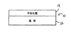
図1を参照しながら、集積回路前駆体10を示す。前駆体10は、基板12および硬化した平坦化層14を含む。図示してないが、前駆体10は、その上に構造または形状を有する表面を含むということを当業者は理解されよう。これらの構造は、前駆体の最終使用目的に応じ、多様な凹凸および形状を有する。ここで用いる「凹凸」は、構造の高さまたは深さをいい、一方「形状」は構造の幅と長さをいう。幅と長さが異なる場合、形状の大きさとして、より小さい数字を基準にすることは通常である。
【0030】
図2は、先にここに記載した従来技術の接触平坦化処理により形成した集積回路前駆体16の断面図を表す。従来技術の前駆体16も、基板18および硬化した平坦化層20を含む。しかしながら、従来技術の接触平坦化処理によって下処理すると、平坦化層20は好ましくない隙間22を有する。これらの隙間の一部は表面でくぼみ22aの形をしている。これらのくぼみ22は、層20の表面にあっても層20の中にあっても、膜の特性を悪化させるので好ましくない。
【0031】
図3は、本発明によって形成した集積回路前駆体24の概略断面図である。本発明の前駆体24は、基板26と硬化した平坦化層28を含む。しかしながら、ここに記載した改善によって、平坦化層28には基本的に従来技術の前駆体16に存在する隙間がない。したがって、本発明により形成した前駆体構造の硬化した平坦化層は、硬化した層の中に約1%よりも少なく、好ましくは約0.5%より少なく、より好ましくは約0%の隙間を有する。ここで用いる「隙間」という用語は、図2に示すように、層の一部が欠落している平坦化層の領域として定義する。これは外部の欠陥(例えば層内の異質の小片)とは区別される。「隙間」は物質内に見いだされる自然な微細孔よりも大きい領域であるということを、当業者は理解されよう。隙間%は、
(1) 50,000倍の倍率に設定された走査型電子顕微鏡で、異なる5つの断面の構造を調べ、
(2) 長さ「L」および高さ「H」の各断面を有する断片の中心付近において(この倍率で)観測される隙間の数を計算し、ここで「L」は約10mm、「H」は約1μmである(図2参照)、
(3) ステップ(2)で計算した隙間の数を用い、各5つのサンプルの硬化した層の中の隙間%を求め、
(4) これら5つの隙間%の平均を決定する、
ことにより決定する。
【0032】
実施例
以下の実施例は、本発明による好ましい方法を記載する。しかしながら、これらの実施例は、例示として提供し、本発明の全範囲の限定とみなすべきでないということが理解される。
【0033】
実施例1〜11では、二酸化ケイ素で被覆し、表面に線状、溝状および正方形の構造を有する6インチのウエハを基板として用いた(SKW1−1 Dielectric Oxide CMP Characterization Wafer、SKW関連より購入)。線状および溝状構造の幅は、約12.5μmから237.5μmである。線状構造の高さおよび溝状構造の深さは約0.9−1.0μmである。ウエハ表面に深さ0.9〜1.0μmの約50μmと2000μmの正方形の穴がある。
【0034】
実施例1
ノボラックエポキシ平坦化物質および真空下での平坦化
10グラムのノボラックエポキシ樹脂(D.E.R.(登録商標)354LV、Dow Chemical Companyより購入した)と0.6グラムの50%ヘキサフルオロリン酸トリアリールスルホニウム(光酸発生剤)溶液(Aldrichより購入した)を含む光硬化性平坦化物質を調製し完全に混合させた。光酸発生剤溶液に用いた溶媒は反応性溶媒(すなわち、プロピレンカーボネート)である。
【0035】
メーカー推奨プロセスを用い、接触促進剤(APX−K1、Brewer Science,Inc.から入手した)によって予め処理した6インチシリコンウエハ表面に、層厚24μmの平坦化物質を被覆した。標準エッジビート除去処理を行い、約5mmのエッジビートを取り除いた。次に、このウエハを接触平坦化処理チャンバー内のウエハ試料台上に、被覆した表面を紫外線透過光学的平坦物体に向き合わせて置いた。圧力チャンバーを密閉し、20トール未満に排気し、ウエハ試料台を上昇させ、ウエハをテフロン(登録商標)リリースフィルムに対して押圧し、このフィルムは68psiの押圧力で30秒間、光学的平坦表面に対して押圧した。平坦化物質が光学的平坦表面に接触している間、(水銀−キセノンランプからの)連続的な紫外線光を、光学的平坦表面を通して10秒間照射し、平坦化物質を硬化した。平坦化物質が硬化するとすぐに押圧力を解放した。ウエハ試料台を降下させ、ウエハをテフロン(登録商標)リリースフィルムから離し、チャンバーを通気した。平坦化した表面の粗さおよび平坦化の程度を明らかにするために、Dektak8(Veeco Metrology Group)を用いた。高さ1μmの原基板構造の中に約200オングストロームの段差高を検出した。約98%の平坦度を達成した。100%の度合いの平坦度は、原構造の段差高が完全に取り除かれていることを示す。平坦化した物質内に隙間は検出されなかった。本発明の方法では、少なくとも約90%、好ましくは少なくとも約95%、より好ましくは少なくとも98%の平坦度になる。
【0036】
実施例2
ノボラックエポキシおよびグリシジルエーテル平坦化物質ならびに
真空下での平坦化
5グラムのノボラックエポキシ樹脂(D.E.R.(登録商標)354LV)、5グラムのn−ブチルグリシジルエーテル(Aldrichから購入した)、および0.6グラムの50%ヘキサフルオロリン酸トリアリールスルホニウム溶液から成る光硬化性平坦化物質を調製し完全に混合させた。光酸発生剤溶液に用いた溶媒はプロピレンカーボネートである。物質を0.2μmフィルターで濾過した。
【0037】
メーカー推奨プロセスを用い、接触促進剤APX−K1によって予め処理した6インチシリコンウエハ表面に、層厚1.5μmの平坦化物質を被覆した。標準エッジビート除去処理を行い、約5mmのエッジビートを取り除いた。このウエハを接触平坦化処理チャンバー内のウエハ試料台上に、被覆した表面を紫外線透過光学的平坦物体に向き合わせて置いた。圧力チャンバーを密閉し、20トール未満に排気し、ウエハ試料台を上昇させ、ウエハをテフロン(登録商標)リリースフィルムに対して押圧し、このフィルムは68psiの押圧力で30秒間、光学的平坦表面に対して押圧した。平坦化物質が光学的平坦表面に接触している間、連続的な紫外線光を、光学的平坦表面を通して10秒間照射し、平坦化物質を硬化した。平坦化物質が硬化するとすぐに押圧力を解放した。ウエハ試料台を降下させ、ウエハをテフロン(登録商標)リリースフィルムから離し、チャンバーを通気した。平坦化した表面の粗さおよび平坦化の程度を明らかにするために、Dektak8を用いた。高さ1μmの原基板構造の中に約200オングストロームの段差高を検出した。約98%の平坦度を達成した。平坦化した物質内に隙間は検出されなかった。
【0038】
n−ブチルグリシジルエーテルをt−ブチルグリシジルエーテル(Aldrichから購入した)に置き換えたことを除いて、本実施例を記載したとおりに繰り返した。約99%の平坦度が、平坦化した物質内に隙間なしに達成された。
【0039】
実施例3
ノボラックエポキシおよびグリシジルエーテル平坦化物質ならびに
周囲圧力での平坦化
5グラムのノボラックエポキシ樹脂(D.E.R.(登録商標)354LV)、5グラムのt−ブチルグリシジルエーテル、および0.6グラムの50%ヘキサフルオロリン酸トリアリールスルホニウム溶液から成る光硬化性平坦化物質を調製し完全に混合させた。光酸発生剤溶液に用いた溶媒はプロピレンカーボネートである。物質を0.2μmフィルターで濾過した。
【0040】
メーカー推奨プロセスを用い、接触促進剤(APX−K1)によって予め処理した6インチシリコンウエハ表面に、層厚1.7μmの平坦化物質を被覆した。標準エッジビート除去処理を行い、約5mmのエッジビートを取り除いた。このウエハを接触平坦化処理チャンバー内のウエハ試料台上に、被覆した表面を紫外線透過光学的平坦物体に向き合わせて置いた。圧力チャンバーを密閉し、20トール未満に排気し、ウエハ試料台を上昇させ、ウエハをテフロン(登録商標)リリースフィルムに対して押圧し、このフィルムは68psiの押圧力で30秒間、光学的平坦表面に対して押圧した。平坦化物質が光学的平坦表面に接触している間、連続的な紫外線光を、光学的平坦表面を通して10秒間照射し、平坦化物質を硬化した。平坦化物質が硬化するとすぐに押圧力を解放した。ウエハ試料台を降下させ、ウエハをテフロン(登録商標)リリースフィルムから離した。平坦化した表面の粗さおよび平坦化の程度を明らかにするために、Dektak8を用いた。高さ1μmの原基板構造の中に約200オングストロームの段差高を検出した。約98%の平坦度を達成した。平坦化した物質内に隙間は検出されなかった。
【0041】
実施例4
ノボラックエポキシおよびビニルエーテル平坦化物質ならびに
真空下での平坦化
5グラムのノボラックエポキシ樹脂(D.E.R.(登録商標)354LV)、5グラムの1,4―シクロヘキサンジメタノールジビニルエーテル(Aldrichから購入した)、および0.6グラムの50%ヘキサフルオロリン酸トリアリールスルホニウム溶液を含む光硬化性平坦化物質を調製し完全に混合させた。光酸発生剤溶液に用いた溶媒はプロピレンカーボネートである。物質を0.2μmフィルターで濾過した。
【0042】
メーカー推奨プロセスを用い、接触促進剤(APX−K1)によって予め処理した6インチシリコンウエハ表面に、層厚2.4μmの平坦化物質を被覆した。標準エッジビート除去処理を行い、約5mmのエッジビートを取り除いた。このウエハを接触平坦化処理チャンバー内のウエハ試料台上に、被覆した表面を紫外線透過光学的平坦物体に向き合わせて置いた。圧力チャンバーを密閉し、20トール未満に排気し、ウエハ試料台を上昇させ、ウエハをテフロン(登録商標)リリースフィルムに対して押圧し、このフィルムは68psiの押圧力で30秒間、光学的平坦表面に対して押圧した。平坦化物質が光学的平坦表面に接触している間、連続的な紫外線光を、光学的平坦表面を通して10秒間照射し、平坦化物質を硬化した。平坦化物質が硬化するとすぐに押圧力を解放した。ウエハ試料台を降下させ、ウエハをテフロン(登録商標)リリースフィルムから離し、チャンバーを通気した。平坦化した表面の粗さおよび平坦化の程度を明らかにするために、Dektak8を用いた。高さ1μmの原基板構造の中に約400オングストロームの段差高を検出した。約96%の平坦度を達成した。平坦化した物質内に隙間は検出されなかった。
【0043】
実施例5
ビニルエーテル平坦化物質および
周囲圧力での紫外線パルス露光による平坦化
10グラムのビス[4−(ビニルオキシ)ブチル]イソフタル酸(VEctomer(登録商標)4010ビニルエーテル、Morflex,Inc.によって販売され、Aldrichから購入した)および0.6グラムの50%ヘキサフルオロリン酸トリアリールスルホニウム溶液を含む光硬化性平坦化物質を調製し完全に混合させた。光酸発生剤溶液に用いた溶媒はプロピレンカーボネートである。
【0044】
メーカー推奨プロセスを用い、接触促進剤(APX−K1)によって予め処理した6インチシリコンウエハ表面に、層厚4.2μmの平坦化物質を被覆した。このウエハを接触平坦化処理チャンバー内のウエハ試料台上に、被覆した表面を紫外線透過光学的平坦物に向き合わせて置いた。圧力チャンバーを密閉し、20トール未満に排気し、ウエハ試料台を上昇させ、ウエハをテフロン(登録商標)リリースフィルムに対して押圧し、このフィルムは68psiの押圧力で30秒間、光学的平坦表面に対して押圧した。平坦化物質が光学的平坦表面に接触している間、連続的な紫外線光を、光学的平坦表面を通して10秒間照射し、その後紫外線を20秒間止め、2度目の10秒間露光を行った。紫外線露光時間の合計は20秒であった。平坦化物質が硬化するとすぐに押圧力を解放した。ウエハ試料台を降下させ、ウエハをテフロン(登録商標)リリースフィルムから離した。平坦化した表面の粗さおよび平坦化の程度を明らかにするために、Dektak8を用いた。高さ1μmの原基板構造の中に約100オングストロームの段差高を検出した。約99%の平坦度を達成した。平坦化した物質内に隙間は検出されなかった。
【0045】
実施例6
ノボラックエポキシおよびビニルエーテル平坦化物質ならびに
周囲圧力での平坦化
10グラムのノボラックエポキシ樹脂D.E.N.(登録商標)431(Dow Chemical Companyから購入した)、10グラムのビス[4−(ビニルオキシ)ブチル]イソフタル酸および0.6グラムの50%ヘキサフルオロリン酸トリアリールスルホニウム溶液を含む光硬化性平坦化物質を調製し完全に混合させた。光酸発生剤溶液に用いた溶媒はプロピレンカーボネートである。
【0046】
メーカー推奨プロセスを用い、接触促進剤(APX−K1)によって予め処理した6インチシリコンウエハ表面に、層厚12.5μmの平坦化物質を被覆した。このウエハを接触平坦化処理チャンバー内のウエハ試料台上に、被覆した表面を紫外線透過光学的平坦物体に向き合わせて置いた。圧力チャンバーを密閉し、20トール未満に排気し、ウエハ試料台を上昇させ、ウエハをテフロン(登録商標)リリースフィルムに対して押圧し、このフィルムは68psiの押圧力で30秒間、光学的平坦表面に対して押圧した。平坦化物質が光学的平坦表面に接触している間、連続的な紫外線光を、光学的平坦表面を通して10秒間照射し、平坦化物質を硬化した。平坦化物質が硬化するとすぐに押圧力を解放した。ウエハ試料台を降下させ、ウエハをテフロン(登録商標)リリースフィルムから離した。平坦化した表面の粗さおよび平坦化の程度を明らかにするために、Dektak8を用いた。高さ1μmの原基板構造の中に約100オングストロームの段差高を検出した。約99%の平坦度を達成した。平坦化した物質内に隙間は検出されなかった。
【0047】
0.08グラムのフッ素含有界面活性剤(FC−4430、3Mから入手した)を平坦化物質に加えたことを除いて、本実施例を記載したとおり繰り返した。同程度の平坦度が、平坦化物質内に隙間なしに得られた。
【0048】
実施例7
エポキシノボラックジアクリレート平坦化物質および
周囲圧力での平坦化
10グラムのビスフェノール−Aエポキシジアクリレート(EBECRYL(登録商標)3200、脂肪族化合物/芳香族化合物エポキシアクリレート混合物、UCB Chemicalsから購入した)、および0.6グラムのDarocur(登録商標)1173(光開始剤、Cibaより入手した)から成る光硬化性平坦化物質を調製し完全に混合させた。
【0049】
メーカー推奨プロセスを用い、接触促進剤(APX−K1)によって予め処理した6インチシリコンウエハ表面に、層厚17.5μmの平坦化物質を被覆した。このウエハを接触平坦化処理チャンバー内のウエハ試料台上に、被覆した表面を紫外線透過光学的平坦物体に向き合わせて置いた。圧力チャンバーを密閉し、20トール未満に排気し、ウエハ試料台を上昇させ、ウエハをテフロン(登録商標)リリースフィルムに対して押圧し、このフィルムは68psiの押圧力で30秒間、光学的平坦表面に対して押圧した。平坦化物質が光学的平坦表面に接触している間、連続的な紫外線光を、光学的平坦表面を通して10秒間照射し、平坦化物質を硬化した。平坦化物質が硬化するとすぐに押圧力を解放した。ウエハ試料台を降下させ、ウエハをテフロン(登録商標)リリースフィルムから離した。平坦化した表面の粗さおよび平坦化の程度を明らかにするために、Dektak8を用いた。高さ1μmの原基板構造の中に約200オングストロームの段差高を検出した。約98%の平坦度を達成した。平坦化した物質内に隙間は検出されなかった。
【0050】
実施例8
エポキシノボラックアクリレートおよびアクリレート希釈剤平坦化物質ならびに
周囲圧力での平坦化
10グラムのEBECRYL(登録商標)3603(UCB Chemicalsより入手した、20%のトリプロピレングリコールジアクリラートで希釈したノボラアックエポキシアクリレートを含む)、および0.6グラムのEBECRYL(登録商標)BPO(光開始剤、UCBChemicalsから入手した)を含む光硬化平坦化物質を調製し完全に混合させた。
【0051】
メーカー推奨プロセスを用い、接触促進剤(APX−K1)によって予め処理した6インチシリコンウエハ表面に、層厚17μmの平坦化物質を被覆した。このウエハを接触平坦化処理チャンバー内のウエハ試料台上に、被覆した表面を紫外線透過光学的平坦物体に向き合わせて置いた。圧力チャンバーを密閉し、20トール未満に排気し、ウエハ試料台を上昇させ、ウエハをテフロン(登録商標)リリースフィルムに対して押圧し、このフィルムは68psiの押圧力で30秒間、光学的平坦表面に対して押圧した。平坦化物質が光学的平坦表面に接触している間、連続的な紫外線光を、光学的平坦表面を通して10秒間照射し、平坦化物質を硬化した。平坦化物質が硬化するとすぐに押圧力を解放した。ウエハ試料台を降下させ、ウエハをテフロン(登録商標)リリースフィルムから離した。平坦化した表面の粗さおよび平坦化の程度を明らかにするために、Dektak8を用いた。高さ1μmの原基板構造の中に約100オングストロームの段差高を検出した。約99%の平坦度を達成した。平坦化した物質内に隙間は検出されなかった。
【0052】
実施例9
ノボラックエポキシおよびアリルグリシジルエーテル平坦化物質ならびに
真空下での平坦化
5グラムのノボラックエポキシ樹脂D.E.N.(登録商標)431(DOW Chemicla Companyより購入した)、5グラムのアリルグリシジルエーテル(Aldrichから購入した)、および0.6グラムの50%ヘキサフルオロリン酸トリアリールスルホニウム溶液より成る光硬化性平坦化物質を調製し完全に混合させた。光酸発生剤溶液に用いた溶媒は炭酸プロピレンである。物質を0.2μmフィルターで濾過した。
【0053】
メーカー推奨プロセスを用い、接触促進剤(APX−K1)によって予め処理した6インチシリコンウエハ表面に、層厚1.8μmの平坦化物質を被覆した。標準エッジビート除去処理を行い、約5mmのエッジビートを取り除いた。このウエハを接触平坦化処理チャンバー内のウエハ試料台上に、被覆した表面を紫外線透過光学的平坦物体に向き合わせて置いた。圧力チャンバーを密閉し、20トール未満に排気し、ウエハ試料台を上昇させ、ウエハをテフロン(登録商標)リリースフィルムに対して押圧し、このフィルムは68psiの押圧力で30秒間、光学的平坦表面に対して押圧した。平坦化物質が光学的平坦表面に接触している間、連続的な紫外線光を、光学的平坦表面を通して10秒間照射し、平坦化物質を硬化した。平坦化物質が硬化するとすぐに押圧力を解放した。ウエハ試料台を降下させ、ウエハをテフロン(登録商標)リリースフィルムから離し、チャンバーを通気した。平坦化した表面の粗さおよび平坦化の程度を明らかにするために、Dektak8を用いた。高さ1μmの原基板構造の中に約100オングストロームの段差高を検出した。約99%の平坦度を達成した。平坦化した物質内に隙間は検出されなかった。
【0054】
実施例10
ノボラックエポキシおよびアリルグリシジルエーテル平坦化物質ならびに
周囲圧力での紫外線パルス露光による平坦化
10グラムのノボラックエポキシ樹脂D.E.N.(登録商標)431、10グラムのアリルグリシジルエーテル、0.09グラムのフッ素含有界面活性剤(FC−4430)、および0.6グラムの50%トリアリールスルホニウムヘキサフルオロリン酸塩溶液から成る光硬化性平坦化物質を調製し完全に混合させた。光酸発生剤溶液に用いた溶媒はプロピレンカーボネートである。
【0055】
メーカー推奨プロセスを用い、接触促進剤(APX−K1)によって予め処理した6インチシリコンウエハ表面に、層厚1.8μmの平坦化物質を被覆した。このウエハを接触平坦化処理チャンバー内のウエハ試料台上に、被覆した表面を紫外線透過光学的平坦物体に向き合わせて置いた。圧力チャンバーを密閉し、20トール未満に排気し、ウエハ試料台を上昇させ、ウエハをテフロン(登録商標)リリースフィルムに対して押圧し、このフィルムは68psiの押圧力で30秒間、光学的平坦表面に対して押圧した。平坦化物質が光学的平坦表面に接触している間、連続的な紫外線光を、光学的平坦表面を通して10秒間照射し、その後紫外線を20秒間止め、2度目の10秒間露光を行った。紫外線露光時間の合計は20秒であった。平坦化物質が硬化するとすぐに押圧力を解放した。ウエハ試料台を降下させ、ウエハをテフロン(登録商標)リリースフィルムから離した。平坦化した表面の粗さおよび平坦化の程度を明らかにするために、Dektak8を用いた。高さ1μmの原基板構造の中に約150オングストロームの段差高を検出した。約98%の平坦度を達成した。平坦化した物質内に隙間は検出されなかった。
【0056】
実施例11
ノボラックエポキシおよびアリルグリシジルエーテル平坦化物質ならびに
周囲圧力での短い押圧時間での平坦化
5グラムのノボラックエポキシ樹脂D.E.N.(登録商標)431、5グラムのアリルグリシジルエーテル、および0.6グラムの50%ヘキサフルオロリン酸トリアリールスルホニウム溶液から成る光硬化性平坦化物質を調製し完全に混合させた。光酸発生剤溶液に用いた溶媒はプロピレンカーボネートである。
【0057】
メーカー推奨プロセスを用い、接触促進剤(APX−K1)によって予め処理した6インチシリコンウエハ表面に、層厚1.8μmの平坦化物質を被覆した。このウエハを接触平坦化処理チャンバー内のウエハ試料台上に、被覆した表面を紫外線透過光学的平坦物体に向き合わせて置いた。圧力チャンバーを密閉し、20トール未満に排気し、ウエハ試料台を上昇させ、ウエハをテフロン(登録商標)リリースフィルムに対して押圧し、このフィルムは68psiの押圧力で30秒間、光学的平坦表面に対して押圧した。平坦化物質が光学的平坦表面に接触している間、連続的な紫外線光を、光学的平坦表面を通して10秒間照射し、平坦化物質を硬化した。平坦化物質が硬化するとすぐに押圧力を解放した。ウエハ試料台を降下させ、ウエハをテフロン(登録商標)リリースフィルムから離し、チャンバーを通気した。平坦化した表面の粗さおよび平坦化の程度を明らかにするために、Dektak8を用いた。高さ1μmの原基板構造の中に約100オングストロームの段差高を検出した。約99%の平坦度を達成した。平坦化した物質内に隙間は検出されなかった。
【0058】
実施例12
ノボラックエポキシおよびグリシジルエーテル平坦化物質ならびに
サブミクロンバイアホール構造の基板を用いての周囲圧力での平坦化
サブミクロンバイアホールを有する、二酸化ケイ素で被覆されたウエハを基板として用いた。バイアホールの直径は0.2μm〜1.0μmの範囲であった。バイアホールの深さは約1.0μmであった。
【0059】
5グラムのノボラックエポキシ樹脂D.E.R.(登録商標)354LV、5グラムのt−ブチルグリシジルエーテル、および0.6グラムの50%ヘキサフルオロリン酸トリアリールスルホニウム溶液を含む光硬化性平坦化物質を調製し完全に混合させた。光酸発生剤溶液に用いた溶媒はプロピレンカーボネートである。
【0060】
メーカー推奨プロセスを用い、接触促進剤(APX−K1)によって予め処理したバイアホールウエハ表面に、層厚約1.7μmの平坦化物質を被覆した。このウエハを接触平坦化処理チャンバー内のウエハ試料台上に、被覆した表面を紫外線透過光学的平坦物体に向き合わせて置いた。圧力チャンバーを密閉し、20トール未満に排気し、ウエハ試料台を上昇させ、ウエハをテフロン(登録商標)リリースフィルムに対して押圧し、このフィルムは68psiの押圧力で30秒間、光学的平坦表面に対して押圧した。平坦化物質が光学的平坦表面に接触している間、連続的な紫外線光を、光学的平坦表面を通して10秒間照射して平坦化物質を硬化した。平坦化物質が硬化するとすぐに押圧力を解放した。ウエハ試料台を降下させ、ウエハをテフロン(登録商標)リリースフィルムから離した。平坦化した表面の粗さおよび平坦化の程度を明らかにするために、Dektak8を用いた。高さ1μmの原基板構造の中に約100オングストロームの段差高を検出した。約99%の平坦度を達成した。平坦化した物質内に隙間は検出されなかった。
【図面の簡単な説明】
【0061】
【図1】基板と基板上の平坦化層を有する回路前駆構造体の概略図である。
【図2】基板と基板上の平坦化層を有する従来技術の前駆構造体の概略断面図である。
【図3】基板と基板上に平坦化層を有する本発明の前駆構造体の概略斜視図である。【Technical field】
[0001]
Background of the Invention
R & D program sponsored by the federal government
The present invention was accomplished with government support based on the Technical Progress Program # 70NANB1H3019 awarded by the National Institute of Standards and Technology (NIST). The US government has certain rights in this invention.
[0002]
Related applications
This application is a benefit of priority over a provisional application entitled Serial Number 60 / 335,811, a contact flattening material free of volatile residues, filed Oct. 31, 2001, which is incorporated herein by reference. Insist.
[0003]
Field of Invention
The present invention broadly relates to thermoplastics, thermosetting materials and photocurable materials used to fabricate microelectronics, optoelectronics, optical, microelectromechanical systems (MEMS) and sensor elements using contact planarization techniques. . These materials essentially do not generate residual volatile components during curing.
[0004]
Description of prior art
New integrated circuit (IC) designs rely heavily on increasingly complex device stacking techniques to create higher performance, lower structure, and less energy demanding semiconductor devices. This requires more circuitry with a finer structure that is integrated into the chip by constructing interconnect and dielectric multilayers on the semiconductor substrate in the proper order. In order to construct an IC, many layers including an ultrafine structure must be formed on a semiconductor surface. In order to construct such an ultra-fine structure, material must be deposited and removed from the surface. Currently, photolithography is a leading technology used to create such ultrafine structures.
[0005]
Photolithography involves depositing a photosensitive material, known as a photoresist, on the surface of a semiconductor substrate. A light transmissive object (known as a photomask or reticle) having a predefined image structure built on a semiconductor surface is placed on a photoresist coated substrate. An appropriate wavelength of light is illuminated through the light transmissive object. Depending on the characteristics of the photoresist and process, the light decomposes or cures the exposed areas of the photoresist. The semiconductor surface is developed to produce a patterned image on the substrate surface, thereby preparing the device for subsequent processing.
[0006]
The conditions necessary for a successful photolithography process are well known to those skilled in the art. For example, it is important to apply the photoresist in a specific uniform thickness to meet the depth of focus requirements required for photolithography processes. Thickness uniformity is related not only to the deposition of other materials on the substrate surface during the manufacture of semiconductor devices, but also during photolithography processes. For example, if the interlayer dielectric is applied with a non-uniform thickness, the process of opening the via cannot completely etch to the bottom of the layer in the thicker dielectric region.
[0007]
If the coated surface is perfectly flat, the material can be applied in an appropriate uniform thickness. However, if the surface is not planar (ie, if the surface is uneven), the material often cannot be coated with a uniform thickness, which can greatly affect the final yield or performance of the device. The coating deposited on the uneven surface tends to reflect the topography of the underlying surface, thus creating a non-planar surface.
[0008]
The multilayer structure of an IC is made by processing one layer on top of another. The first layer of the structure is formed on a planar semiconductor surface. As a result, the uneven surface is taken in on the semiconductor substrate surface. The second layer is formed on the uneven surface of the layer of the first structure. As more layers are formed on the substrate, the degree of surface irregularities increases. A non-planar surface is no longer suitable for constituting the next structural layer. Therefore, it is necessary to flatten or flatten the uneven surface before forming the next layer. Plasma planarization, chemical mechanical polishing (CMP) and contact planarization techniques are typically used to planarize the uneven surface.
[0009]
Plasma etch back is a technique that involves the deposition of a thick film to smooth the underlying uneven surface to some extent. Better surface flatness can be achieved with a thicker film. However, longer plasma etching times are required to etch thicker films. The deposited film must have a plasma etch rate that closely matches the underlying relief layer material under certain etching parameters. Thereafter, in order to improve the surface flatness, the thick film is etched by plasma etching to the lower uneven layer.
[0010]
The chemical mechanical polishing technique is a technique that uses a slurry liquid and mechanically polishes the surface in contact with the pad using a chemical reaction that occurs between the substrate material and the slurry liquid. The slurry liquid contains abrasive particles and provides a specific chemical to the pad surface. The uneven substrate surface is pressed in contact with the pad. The substrate is then polished in a circular motion in contact with the pad to remove surface irregularities. Chemical mechanical polishing is currently used in IC manufacturing. Specific requirements necessary for planarization and processing conditions for specific materials are known to those skilled in the art.
[0011]
Contact planarization provides an alternative to plasma etchback and chemical mechanical polishing techniques to planarize uneven surfaces. First, a planarizing material having fluidity is deposited on the uneven surface. The surface is then pressed by an optically flat surface to allow the material to flow around the irregular surface under certain conditions. Next, the material is cured by either light irradiation or heating so that the planarity of the optical flat surface is transferred to the material surface to be planarized. The surface of the planarized material is separated from the optically flat object surface. In order to facilitate separation, the optically flat object surface can be treated to reduce its surface energy. This can be accomplished by depositing a thin film of a low surface energy material such as a fluoropolymer or fluorine compound on the optically flat object surface. Another approach is to place a low surface energy material, such as a disk or film, having the same degree of surface planarity between the planarizing material and the optically flat object surface. Examples of low surface energy materials include materials sold under names such as Teflon (registered trademark), fluororesin and the like. The planarized material surface is plasma etched down to the underlying concavo-convex layer to transfer the planarity of the optically flat surface to the underlying concavo-convex layer, thereby planarizing the concavo-convex surface. One requirement for the planarized material is that it should have a plasma etch rate of about 1 relative to the plasma etch rate of the underlying relief layer material.
[0012]
Currently, materials used for contact planarization and similar techniques include volatile organic solvents that can remain in the cured film and can cause the formation of bubbles in the film during the curing process. These bubbles form gaps and are permanently trapped in the film during curing. If bubbles are formed between the contact surface of the planarizing material and the optically planar surface, a rough surface results. In addition, confined bubbles will degrade not only membrane integrity but also membrane properties. Additional processing and conditions such as pre-baking or post-baking techniques, high temperature processing, vacuum processing environment, or combinations thereof are required to remove residual solvent from the film prior to curing to prevent bubble formation. is there. Removal of residual solvent can cause film shrinkage. Shrinkage results in undesirable irregularities on the surface because the thickness of the material being planarized across the substrate surface varies. Shrinkage is more severe above the underlying recessed area where thicker planarizing material is deposited. Accordingly, the flatness of the surface is lowered.
[0013]
As described above, the contact planarization process relies on an optical planar surface that contacts the material surface to be planarized, which is confined and planarized between the two surfaces. To flow. Both the optically flat surface and the flattened surface cannot be penetrated by volatile vapors. During the planarization process, if the planarization material contains a volatile and non-reactive solvent or produces a volatile byproduct, the volatile material will be trapped between the two surfaces. When the planarizing material is cured during the planarization process, the residual solvent will evaporate. Evaporation occurs due to heat generated during light irradiation (if a photocuring planarizing material is used) or heat applied to the thermosetting planarizing material during curing. During contact planarization, the planarized material surface is subjected to a plasma etch process to transfer the planarity of the planarized surface to the underlying irregular surface. Residual solvent is released during the plasma etch process, which in turn changes the plasma chemical reaction in the etch apparatus. As a result, the plasma etch rate and the etch rate rate change, and as a result, the surface flatness of the etched surface deteriorates. If the residual solvent is not evenly distributed within the planarized material, even if the residual solvent is removed after the planarization process, undesirable gaps will be formed at the planarized material or contact interface. If the solvent vapor is confined to the interface between the planarizing material and the optical surface, these gaps will cause a rough surface that degrades the planarity of the planarized material surface. If the solvent is confined to a flattened material, the gap will undesirably cause a non-uniform material density throughout the thickness of the material. More importantly, the plasma etch rate is faster for regions with more and larger gaps than for regions with fewer gaps. As a result, the planarity of the etched surface is degraded due to the non-uniform plasma etch rate. Moreover, these gaps are likely to collect in small holes such as trenches, vias and holes that are most important for device manufacture.
[0014]
Alternatively, the chemical mechanical polishing process can transfer the planarized surface planarity to the underlying layer if it can achieve a consistent chemical mechanical polishing removal rate between the planarizing material and the underlying material. . In order to obtain a constant and uniform chemical mechanical polishing removal rate while polishing the material, a constant and uniform material density is required. If there is a gap in the material, the size of the gap is not the same, and if it is not evenly distributed over the entire range of the material, it will have a negative impact on achieving a constant and uniform chemical mechanical polishing removal rate. Effect. Therefore, to achieve a consistent removal rate while polishing the planarization material and the underlying material simultaneously, it has a constant and uniform density to ensure a constant and uniform chemical mechanical polishing removal rate within the planarization material. A flattened film without gaps is necessary.
[0015]
In general, the polymerization process can be classified into condensation polymerization and addition polymerization (Stevens, Malcolm P., Polymer Chemistry: Preface, Chapter 1, Oxford University Press, 1990, shown here for reference). . The polymer formed through the condensation polymerization process contains fewer atoms than the atoms in the monomer in the repeating unit because a by-product is generated during the polymerization process. The polymer formed through the addition polymerization process has the same number of atoms as the monomer in the repeating unit. Some polymers can be synthesized by either condensation or polymerization processes, depending on the choice of polymerization starting materials. The polymerization process may require the addition of a polymerization starting material or catalyst and further a polymerization mechanism. The polymerization process can be triggered by light irradiation or heating, depending on the design and configuration of the planarizing material.
[0016]
Prybyla et al. U.S. Pat. No. 6,048,799 states that a planarizing material having a tack of about 20 centipoise (cP) to 40,000 cP is used during the planarization step. The material can be cured by heating or UV irradiation. However, this approach does not mention the effect of residual solvent in the planarized material, nor does it mention the possibility of generating volatile by-products that may occur during solidification. If there is residual solvent in the planarized film and it is not evenly distributed throughout the film, once the residual solvent is removed from the film, it will cause a density gradient in the planarized material.
[0017]
Summary of the Invention
The present invention relates to novel microelectronic precursors and methods of forming such precursors.
[0018]
More specifically, the precursor is formed by first providing a planarizing layer (for example, spin coating, spray coating, casting, paddle method, fountain coating, etc.) on a microelectronic substrate having a concavo-convex shape on the surface. This layer is usually formed to a thickness of about 0.1 to 500 μm (preferably about 0.2 to 200 μm), and the thickness of this layer is preferably larger than the height of the surface irregular shape. Typical microelectronic substrates include silicon wafers, semiconductor wafer composites, glass substrates, quartz substrates, polymers, dielectric substrates, metals, alloys, silicon carbide, silicon nitride, sapphire, and ceramics.
[0019]
The planarization layer is formed of a material including a material selected from the group consisting of photocurable or thermosetting monomers, oligomers, and combinations thereof. These planarizing materials must be cured (polymerized) via an addition polymerization mechanism that produces substantially no volatile byproducts (more preferably no volatile byproducts). If the total weight of the planarizing material is 100% by weight, the total weight of monomers and / or oligomers in the material is at least about 10% by weight, preferably about 15-100% by weight. Suitable monomers and oligomers include epoxies, novolac epoxies, acrylates, novolac epoxy acrylates, vinyl ethers, novolac epoxy vinyl ethers, vinyl containing organic and inorganic monomers / oligomers, and mixtures thereof.
[0020]
The substance preferably further comprises a reactive solvent. The reactive solvent used here reacts with monomers, oligomers or mixtures thereof to form a polymer (conventional polymerization reaction), and the reactive solvent is consumed considerably in this reaction. Thus, the reactive solvent acts as a comonomer. When a reactive solvent is used, the reactive solvent should be present at a level of about 1 to 90% by weight, preferably about 10 to 50% by weight, with the total weight of the material being 100% by weight. Suitable reactive solvents are not necessarily determined by the monomer or oligomer used, but are typically propylene carbonate, glycidyl ether, vinyl ether, allyl ether, acrylate, other monofunctional or polyfunctional reactive solvents, and Including these mixtures.
[0021]
The substance preferably further comprises a component selected from the group consisting of acids, acid generators (eg, thermal acid generators, photoacid generators) and surfactants. If acids or acid generators are present, they should be present at a level of about 0.1 to 10% by weight, preferably about 0.5 to 3% by weight, assuming the total weight of the material is 100% by weight. is there. Suitable acids or acid generators include triarylsulfonium hexafluorophosphate, triarylsulfonium hexafluoroarsenate, diaryliodonium hexafluorophosphate, diaryliodonium hexafluoroantimonate, diaryliodonium hexafluoroarsenate, hexaaryl Including those selected from the group consisting of triarylsulfoxonium fluorophosphates and aryloxysulfoxonium hexafluorophosphates.
[0022]
The surfactant, if present, should be non-volatile and is about 0.01 to 3% by weight, preferably about 0.05 to 0.5% by weight, with the total weight of the material being 100% by weight. Should be used at the level of Suitable surfactants include fluorine-containing surfactants and polymeric surfactants.
[0023]
In particularly preferred embodiments, the planarizing material includes very low levels of non-reactive solvents or diluents (eg, PGME, PGMEA). Accordingly, the planarizing material includes less than about 5% by weight of non-reactive solvent or diluent, preferably less than about 2% by weight, where the total weight of the planarizing material is 100%. Even more preferably, the planarizing material is essentially free of non-reactive solvents or diluents.
[0024]
Regardless of the components contained within the planarizing material, the planarizing material should have a tackiness of about 10 to 50,000 cP, preferably about 10 to 5,000 cP. Thus, the material can fill cracks having a size of about 0.1 μm or more, preferably in the range of 0.2 to 50,000 μm.
[0025]
After adding the planarizing material, remove the edge beats if necessary and allow the material to contact the planar object with the layer for a sufficient amount of time and pressure to transfer the planar surface of the object to the planarizing layer. . The contacting or pressing step typically includes applying a pressure of about 5 to 200 psi, more preferably about 10 to 100 psi, for about 1 second to about 10 minutes, preferably about 10 to 60 seconds.
[0026]
The contacting step is usually performed at a temperature of about 18 to 400 ° C, more preferably about 18 to 150 ° C. However, if a thermoplastic material is present in the planarizing material, the temperature used is highly material dependent. As long as temperature is involved in this situation, the pressing step is approximately T of the planarizing material.g Preferably, the temperature is about 20 ° C. higher than the melting point of the planarizing material. Even more preferably, the temperature is about 5 ° C. to about 10 ° C. higher than the melting point of the substance.
[0027]
This treatment can be performed in a vacuum chamber below about 20 Torr, but is equally preferred at ambient conditions. To apply this pressure, an optical flat or another equivalent means can be used, and the pressure application means selected must be selected to suit a particular process (eg, using an ultraviolet curing process). It will be appreciated that UV transmission optical flatness is required.
[0028]
While the optical planar object and the substrate are held in contact, the planarizing material is consolidated or cured by conventional means. For example, if the composition is photocurable, ultraviolet light (with a wavelength appropriate for the particular composition) is applied to cure the layer. Similarly, if the composition is thermoset, it is heated (eg, by hot plate, oven, infrared heating) and then the composition Tg It can be cured by cooling to a lower temperature, preferably below about 50 ° C. Regardless of the curing agent or curing means, the flat object is finally separated from the planarization layer to yield a precursor that can be further processed.
[0029]
Detailed Description of the Preferred Embodiment
With reference to FIG. 1, an
[0030]
FIG. 2 depicts a cross-sectional view of an integrated circuit precursor 16 formed by the prior art contact planarization process previously described herein. The prior art precursor 16 also includes a substrate 18 and a hardened planarization layer 20. However, when pretreated by a prior art contact planarization process, the planarization layer 20 has undesirable gaps 22. Some of these gaps are in the form of indentations 22a on the surface. These indentations 22 are not preferable because they deteriorate the characteristics of the film, whether on the surface of the layer 20 or in the layer 20.
[0031]
FIG. 3 is a schematic cross-sectional view of an integrated circuit precursor 24 formed in accordance with the present invention. The precursor 24 of the present invention includes a substrate 26 and a hardened planarization layer 28. However, with the improvements described herein, the planarization layer 28 is essentially free of gaps present in the prior art precursor 16. Accordingly, a cured planarized layer of precursor structure formed in accordance with the present invention provides less than about 1%, preferably less than about 0.5%, more preferably about 0% gap in the cured layer. Have. As used herein, the term “gap” is defined as a region of the planarization layer in which a part of the layer is missing, as shown in FIG. This is indistinguishable from external defects (eg, extraneous pieces in the layer). One skilled in the art will appreciate that “gaps” are areas larger than the natural micropores found in the material. The gap% is
(1) With a scanning electron microscope set at a magnification of 50,000 times, the structure of five different cross sections was examined,
(2) Calculate the number of gaps observed (at this magnification) near the center of a fragment having cross sections of length “L” and height “H”, where “L” is about 10 mm, “H” Is about 1 μm (see FIG. 2),
(3) Using the number of gaps calculated in step (2), determine the gap% in the cured layer of each of the five samples,
(4) Determine the average of these five gaps%,
To decide.
[0032]
Example
The following examples describe preferred methods according to the present invention. However, it is understood that these examples are provided by way of illustration and should not be considered as limiting the full scope of the invention.
[0033]
In Examples 1 to 11, a 6-inch wafer covered with silicon dioxide and having a linear, groove-like, and square structure on the surface was used as a substrate (purchased from SKW1-1 Dielectric Oxide CMP Characterization Wafer, SKW-related) . The width of the linear and grooved structures is about 12.5 μm to 237.5 μm. The height of the linear structure and the depth of the groove-like structure are about 0.9-1.0 μm. There are approximately 50 μm and 2000 μm square holes with a depth of 0.9 to 1.0 μm on the wafer surface.
[0034]
Example 1
Novolac epoxy planarizing material and planarization under vacuum
10 grams of novolak epoxy resin (DER® 354LV, purchased from Dow Chemical Company) and 0.6 grams of 50% triarylsulfonium hexafluorophosphate (photoacid generator) solution (Aldrich) A photocurable planarizing material was prepared and thoroughly mixed. The solvent used for the photoacid generator solution is a reactive solvent (ie, propylene carbonate).
[0035]
Using a manufacturer-recommended process, a planarizing material having a layer thickness of 24 μm was coated on a 6-inch silicon wafer surface previously treated with a contact promoter (APX-K1, obtained from Brewer Science, Inc.). A standard edge beat removal process was performed to remove an edge beat of about 5 mm. The wafer was then placed on a wafer sample stage in a contact flattening chamber with the coated surface facing an ultraviolet transparent optically flat object. The pressure chamber is sealed, evacuated to less than 20 Torr, the wafer sample stage is raised, and the wafer is pressed against the Teflon release film, which is an optically flat surface for 30 seconds with a pressing force of 68 psi. Pressed against. While the planarizing material was in contact with the optical planar surface, continuous UV light (from a mercury-xenon lamp) was irradiated through the optical planar surface for 10 seconds to cure the planarizing material. The pressing force was released as soon as the planarizing material was cured. The wafer sample stage was lowered, the wafer was separated from the Teflon release film, and the chamber was vented. Dektak 8 (Veeco Metrology Group) was used to reveal the roughness of the planarized surface and the degree of planarization. A step height of about 200 angstroms was detected in the original substrate structure having a height of 1 μm. A flatness of about 98% was achieved. A degree of flatness of 100% indicates that the step height of the original structure has been completely removed. No gaps were detected in the flattened material. The method of the present invention results in a flatness of at least about 90%, preferably at least about 95%, more preferably at least 98%.
[0036]
Example 2
Novolac epoxy and glycidyl ether planarizing materials and
Flattening under vacuum
5 grams of novolak epoxy resin (DER® 354LV), 5 grams of n-butyl glycidyl ether (purchased from Aldrich), and 0.6 grams of 50% triarylsulfonium hexafluorophosphate A photocurable planarizing material consisting of a solution was prepared and mixed thoroughly. The solvent used for the photoacid generator solution is propylene carbonate. The material was filtered through a 0.2 μm filter.
[0037]
Using a manufacturer recommended process, a 6-inch silicon wafer surface pretreated with contact promoter APX-K1 was coated with a planarizing material having a layer thickness of 1.5 μm. A standard edge beat removal process was performed to remove an edge beat of about 5 mm. The wafer was placed on a wafer sample stage in a contact flattening chamber with the coated surface facing an ultraviolet transparent optically flat object. The pressure chamber is sealed, evacuated to less than 20 Torr, the wafer sample stage is raised, and the wafer is pressed against the Teflon release film, which is an optically flat surface for 30 seconds with a pressing force of 68 psi. Pressed against. While the planarizing material was in contact with the optical planar surface, continuous UV light was irradiated through the optical planar surface for 10 seconds to cure the planarizing material. The pressing force was released as soon as the planarizing material was cured. The wafer sample stage was lowered, the wafer was separated from the Teflon (registered trademark) release film, and the chamber was vented. Dektak 8 was used to reveal the roughness of the planarized surface and the degree of planarization. A step height of about 200 angstroms was detected in the original substrate structure having a height of 1 μm. A flatness of about 98% was achieved. No gaps were detected in the flattened material.
[0038]
This example was repeated as described, except that n-butyl glycidyl ether was replaced with t-butyl glycidyl ether (purchased from Aldrich). A flatness of about 99% was achieved without gaps in the flattened material.
[0039]
Example 3
Novolac epoxy and glycidyl ether planarizing materials and
Flattening at ambient pressure
Photocurability consisting of 5 grams of novolac epoxy resin (DER® 354LV), 5 grams of t-butyl glycidyl ether, and 0.6 grams of 50% triarylsulfonium hexafluorophosphate solution. A planarizing material was prepared and mixed thoroughly. The solvent used for the photoacid generator solution is propylene carbonate. The material was filtered through a 0.2 μm filter.
[0040]
Using a manufacturer recommended process, a 6 inch silicon wafer surface previously treated with a contact accelerator (APX-K1) was coated with a planarizing material having a layer thickness of 1.7 μm. A standard edge beat removal process was performed to remove an edge beat of about 5 mm. The wafer was placed on a wafer sample stage in a contact flattening chamber with the coated surface facing an ultraviolet transparent optical flat object. The pressure chamber is sealed, evacuated to less than 20 Torr, the wafer sample stage is raised, and the wafer is pressed against the Teflon release film, which is an optically flat surface for 30 seconds with a pressing force of 68 psi. Pressed against. While the planarizing material was in contact with the optical planar surface, continuous UV light was irradiated through the optical planar surface for 10 seconds to cure the planarizing material. The pressing force was released as soon as the planarizing material was cured. The wafer sample stage was lowered and the wafer was separated from the Teflon release film. Dektak 8 was used to reveal the roughness of the planarized surface and the degree of planarization. A step height of about 200 angstroms was detected in the original substrate structure having a height of 1 μm. A flatness of about 98% was achieved. No gaps were detected in the flattened material.
[0041]
Example 4
Novolac epoxy and vinyl ether planarizing materials and
Flattening under vacuum
5 grams of novolak epoxy resin (DER® 354LV), 5 grams of 1,4-cyclohexanedimethanol divinyl ether (purchased from Aldrich), and 0.6 grams of 50% hexafluorophosphorus A photocurable planarizing material containing a triarylsulfonium acid solution was prepared and mixed thoroughly. The solvent used for the photoacid generator solution is propylene carbonate. The material was filtered through a 0.2 μm filter.
[0042]
Using a manufacturer recommended process, a 6-inch silicon wafer surface pretreated with a contact promoter (APX-K1) was coated with a planarizing material having a layer thickness of 2.4 μm. A standard edge beat removal process was performed to remove an edge beat of about 5 mm. The wafer was placed on a wafer sample stage in a contact flattening chamber with the coated surface facing an ultraviolet transparent optically flat object. The pressure chamber is sealed, evacuated to less than 20 Torr, the wafer sample stage is raised, and the wafer is pressed against the Teflon release film, which is an optically flat surface for 30 seconds with a pressing force of 68 psi. Pressed against. While the planarizing material was in contact with the optical planar surface, continuous UV light was irradiated through the optical planar surface for 10 seconds to cure the planarizing material. The pressing force was released as soon as the planarizing material was cured. The wafer sample stage was lowered, the wafer was separated from the Teflon (registered trademark) release film, and the chamber was vented. Dektak 8 was used to reveal the roughness of the planarized surface and the degree of planarization. A step height of about 400 angstroms was detected in the original substrate structure having a height of 1 μm. A flatness of about 96% was achieved. No gaps were detected in the flattened material.
[0043]
Example 5
Vinyl ether planarizing materials and
Planarization by UV pulse exposure at ambient pressure
10 grams of bis [4- (vinyloxy) butyl] isophthalic acid (VEctomer® 4010 vinyl ether, sold by Morflex, Inc. and purchased from Aldrich) and 0.6 grams of 50% triaryl hexafluorophosphate A photocurable planarizing material containing a sulfonium solution was prepared and mixed thoroughly. The solvent used for the photoacid generator solution is propylene carbonate.
[0044]
Using a manufacturer recommended process, a planarizing material having a layer thickness of 4.2 μm was coated on a 6-inch silicon wafer surface pretreated with a contact accelerator (APX-K1). The wafer was placed on a wafer sample stage in a contact flattening chamber with the coated surface facing an ultraviolet transmission optical flat. The pressure chamber is sealed, evacuated to less than 20 Torr, the wafer sample stage is raised, and the wafer is pressed against a Teflon release film, which is an optically flat surface for 30 seconds with a pressing force of 68 psi. Pressed against. While the planarizing material was in contact with the optical flat surface, continuous ultraviolet light was irradiated through the optical flat surface for 10 seconds, after which the ultraviolet light was stopped for 20 seconds and a second 10 second exposure was performed. The total ultraviolet exposure time was 20 seconds. The pressing force was released as soon as the planarizing material was cured. The wafer sample stage was lowered and the wafer was separated from the Teflon release film. Dektak 8 was used to reveal the roughness of the planarized surface and the degree of planarization. A step height of about 100 angstroms was detected in the original substrate structure having a height of 1 μm. A flatness of about 99% was achieved. No gaps were detected in the flattened material.
[0045]
Example 6
Novolac epoxy and vinyl ether planarizing materials and
Flattening at ambient pressure
10 grams of novolac epoxy resin E. N. (R) 431 (purchased from Dow Chemical Company), a light-curing flat comprising 10 grams of bis [4- (vinyloxy) butyl] isophthalic acid and 0.6 grams of 50% triarylsulfonium hexafluorophosphate solution. Chemicals were prepared and mixed thoroughly. The solvent used for the photoacid generator solution is propylene carbonate.
[0046]
Using a manufacturer recommended process, a planarizing material having a layer thickness of 12.5 μm was coated on a 6-inch silicon wafer surface pretreated with a contact accelerator (APX-K1). The wafer was placed on a wafer sample stage in a contact flattening chamber with the coated surface facing an ultraviolet transparent optically flat object. The pressure chamber is sealed, evacuated to less than 20 Torr, the wafer sample stage is raised, and the wafer is pressed against the Teflon release film, which is an optically flat surface for 30 seconds with a pressing force of 68 psi. Pressed against. While the planarizing material was in contact with the optical planar surface, continuous UV light was irradiated through the optical planar surface for 10 seconds to cure the planarizing material. The pressing force was released as soon as the planarizing material was cured. The wafer sample stage was lowered and the wafer was separated from the Teflon release film. Dektak 8 was used to reveal the roughness of the planarized surface and the degree of planarization. A step height of about 100 angstroms was detected in the original substrate structure having a height of 1 μm. A flatness of about 99% was achieved. No gaps were detected in the flattened material.
[0047]
This example was repeated as described, except that 0.08 grams of fluorine containing surfactant (obtained from FC-4430, 3M) was added to the planarizing material. A similar degree of flatness was obtained without gaps in the planarizing material.
[0048]
Example 7
Epoxy novolac diacrylate planarizing materials and
Flattening at ambient pressure
10 grams of bisphenol-A epoxy diacrylate (EBECRYL® 3200, aliphatic / aromatic epoxy acrylate mixture, purchased from UCB Chemicals), and 0.6 grams of Darocur® 1173 (photo initiation A photo-curing planarizing material consisting of an agent (obtained from Ciba) was prepared and mixed thoroughly.
[0049]
Using a manufacturer recommended process, a planarizing material having a layer thickness of 17.5 μm was coated on the surface of a 6-inch silicon wafer previously treated with a contact accelerator (APX-K1). The wafer was placed on a wafer sample stage in a contact flattening chamber with the coated surface facing an ultraviolet transparent optically flat object. The pressure chamber is sealed, evacuated to less than 20 Torr, the wafer sample stage is raised, and the wafer is pressed against the Teflon release film, which is an optically flat surface for 30 seconds with a pressing force of 68 psi. Pressed against. While the planarizing material was in contact with the optical planar surface, continuous UV light was irradiated through the optical planar surface for 10 seconds to cure the planarizing material. The pressing force was released as soon as the planarizing material was cured. The wafer sample stage was lowered and the wafer was separated from the Teflon release film. Dektak 8 was used to reveal the roughness of the planarized surface and the degree of planarization. A step height of about 200 angstroms was detected in the original substrate structure having a height of 1 μm. A flatness of about 98% was achieved. No gaps were detected in the flattened material.
[0050]
Example 8
Epoxy novolac acrylate and acrylate diluent planarizing materials and
Flattening at ambient pressure
10 grams of EBECRYL® 3603 (containing Novolak epoxy acrylate diluted with 20% tripropylene glycol diacrylate obtained from UCB Chemicals) and 0.6 grams of EBECRYL® BPO ( A photocured planarizing material containing photoinitiator (obtained from UCB Chemicals) was prepared and mixed thoroughly.
[0051]
Using a manufacturer recommended process, a planarizing material having a layer thickness of 17 μm was coated on the surface of a 6-inch silicon wafer previously treated with a contact accelerator (APX-K1). The wafer was placed on a wafer sample stage in a contact flattening chamber with the coated surface facing an ultraviolet transparent optically flat object. The pressure chamber is sealed, evacuated to less than 20 Torr, the wafer sample stage is raised, and the wafer is pressed against the Teflon release film, which is an optically flat surface for 30 seconds with a pressing force of 68 psi. Pressed against. While the planarizing material was in contact with the optical planar surface, continuous UV light was irradiated through the optical planar surface for 10 seconds to cure the planarizing material. The pressing force was released as soon as the planarizing material was cured. The wafer sample stage was lowered and the wafer was separated from the Teflon release film. Dektak 8 was used to reveal the roughness of the planarized surface and the degree of planarization. A step height of about 100 angstroms was detected in the original substrate structure having a height of 1 μm. A flatness of about 99% was achieved. No gaps were detected in the flattened material.
[0052]
Example 9
Novolac epoxy and allyl glycidyl ether planarizing materials and
Flattening under vacuum
5 grams of novolac epoxy resin E. N. Photocurable planarization consisting of 431 (purchased from DOW Chemical Company), 5 grams of allyl glycidyl ether (purchased from Aldrich), and 0.6 grams of 50% triarylsulfonium hexafluorophosphate solution. The material was prepared and mixed thoroughly. The solvent used for the photoacid generator solution is propylene carbonate. The material was filtered through a 0.2 μm filter.
[0053]
Using a manufacturer recommended process, a 6 inch silicon wafer surface previously treated with a contact accelerator (APX-K1) was coated with a planarizing material having a layer thickness of 1.8 μm. A standard edge beat removal process was performed to remove an edge beat of about 5 mm. The wafer was placed on a wafer sample stage in a contact flattening chamber with the coated surface facing an ultraviolet transparent optically flat object. The pressure chamber is sealed, evacuated to less than 20 Torr, the wafer sample stage is raised, and the wafer is pressed against the Teflon release film, which is an optically flat surface for 30 seconds with a pressing force of 68 psi. Pressed against. While the planarizing material was in contact with the optical planar surface, continuous UV light was irradiated through the optical planar surface for 10 seconds to cure the planarizing material. The pressing force was released as soon as the planarizing material was cured. The wafer sample stage was lowered, the wafer was separated from the Teflon release film, and the chamber was vented. Dektak 8 was used to reveal the roughness of the planarized surface and the degree of planarization. A step height of about 100 angstroms was detected in the original substrate structure having a height of 1 μm. A flatness of about 99% was achieved. No gaps were detected in the flattened material.
[0054]
Example 10
Novolac epoxy and allyl glycidyl ether planarizing materials and
Planarization by UV pulse exposure at ambient pressure
10 grams of novolac epoxy resin E. N. Photocuring consisting of 速 431, 10 grams allyl glycidyl ether, 0.09 grams fluorine containing surfactant (FC-4430), and 0.6 grams 50% triarylsulfonium hexafluorophosphate solution. A leveling material was prepared and mixed thoroughly. The solvent used for the photoacid generator solution is propylene carbonate.
[0055]
Using a manufacturer recommended process, a 6 inch silicon wafer surface previously treated with a contact accelerator (APX-K1) was coated with a planarizing material having a layer thickness of 1.8 μm. The wafer was placed on a wafer sample stage in a contact flattening chamber with the coated surface facing an ultraviolet transparent optically flat object. The pressure chamber is sealed, evacuated to less than 20 Torr, the wafer sample stage is raised, and the wafer is pressed against the Teflon release film, which is an optically flat surface for 30 seconds with a pressing force of 68 psi. Pressed against. While the planarizing material was in contact with the optical flat surface, continuous ultraviolet light was irradiated through the optical flat surface for 10 seconds, after which the ultraviolet light was stopped for 20 seconds and a second 10 second exposure was performed. The total ultraviolet exposure time was 20 seconds. The pressing force was released as soon as the planarizing material was cured. The wafer sample stage was lowered and the wafer was separated from the Teflon release film. Dektak 8 was used to reveal the roughness of the planarized surface and the degree of planarization. A step height of about 150 angstroms was detected in the original substrate structure having a height of 1 μm. A flatness of about 98% was achieved. No gaps were detected in the flattened material.
[0056]
Example 11
Novolac epoxy and allyl glycidyl ether planarizing materials and
Flattening with short pressing time at ambient pressure
5 grams of novolac epoxy resin E. N. A photocurable planarizing material consisting of 431, 5 grams of allyl glycidyl ether, and 0.6 grams of 50% triarylsulfonium hexafluorophosphate solution was prepared and mixed thoroughly. The solvent used for the photoacid generator solution is propylene carbonate.
[0057]
Using a manufacturer recommended process, a 6-inch silicon wafer surface previously treated with a contact promoter (APX-K1) was coated with a planarizing material having a layer thickness of 1.8 μm. The wafer was placed on a wafer sample stage in a contact flattening chamber with the coated surface facing an ultraviolet transparent optical flat object. The pressure chamber is sealed, evacuated to less than 20 Torr, the wafer sample stage is raised, and the wafer is pressed against a Teflon release film, which is an optically flat surface for 30 seconds with a pressing force of 68 psi. Pressed against. While the planarizing material was in contact with the optical planar surface, continuous UV light was irradiated through the optical planar surface for 10 seconds to cure the planarizing material. The pressing force was released as soon as the planarizing material was cured. The wafer sample stage was lowered, the wafer was separated from the Teflon (registered trademark) release film, and the chamber was vented. Dektak 8 was used to reveal the roughness of the planarized surface and the degree of planarization. A step height of about 100 angstroms was detected in the original substrate structure having a height of 1 μm. A flatness of about 99% was achieved. No gaps were detected in the flattened material.
[0058]
Example 12
Novolac epoxy and glycidyl ether planarizing materials and
Planarization at ambient pressure using a substrate with a submicron via hole structure
A silicon dioxide coated wafer with submicron via holes was used as the substrate. The via hole diameter ranged from 0.2 μm to 1.0 μm. The depth of the via hole was about 1.0 μm.
[0059]
5 grams of novolac epoxy resin E. R. A photocurable planarizing material containing 354LV, 5 grams of t-butyl glycidyl ether, and 0.6 grams of 50% triarylsulfonium hexafluorophosphate solution was prepared and mixed thoroughly. The solvent used for the photoacid generator solution is propylene carbonate.
[0060]
Using a manufacturer recommended process, a via hole wafer surface pretreated with a contact promoter (APX-K1) was coated with a planarizing material having a layer thickness of about 1.7 μm. The wafer was placed on a wafer sample stage in a contact flattening chamber with the coated surface facing an ultraviolet transparent optical flat object. The pressure chamber is sealed, evacuated to less than 20 Torr, the wafer sample stage is raised, and the wafer is pressed against the Teflon release film, which is an optically flat surface for 30 seconds with a pressing force of 68 psi. Pressed against. While the planarizing material was in contact with the optical planar surface, continuous ultraviolet light was irradiated through the optical planar surface for 10 seconds to cure the planarizing material. The pressing force was released as soon as the planarizing material was cured. The wafer sample stage was lowered and the wafer was separated from the Teflon release film. Dektak 8 was used to reveal the roughness of the planarized surface and the degree of planarization. A step height of about 100 angstroms was detected in the original substrate structure having a height of 1 μm. A flatness of about 99% was achieved. No gaps were detected in the flattened material.
[Brief description of the drawings]
[0061]
FIG. 1 is a schematic diagram of a circuit precursor structure having a substrate and a planarization layer on the substrate.
FIG. 2 is a schematic cross-sectional view of a prior art precursor structure having a substrate and a planarization layer on the substrate.
FIG. 3 is a schematic perspective view of a precursor structure of the present invention having a substrate and a planarization layer on the substrate.
Claims (31)
Translated fromJapanese表面を有し前記表面に複数の凹凸形状を有する基板を提供するステップと、
前記表面に平坦化層を形成するステップとを含み、前記平坦化層は、モノマー、オリゴマー、またはモノマーとオリゴマーの混合物と、反応性溶媒とを含み、
該平坦化層を物体の平坦表面に十分な時間と圧力で接触させて平坦表面の平坦性を平坦化層に転写するステップを含む方法。A method of forming a microelectronic precursor comprising:
Providing a substrate having a surface and a plurality of irregularities on the surface;
Forming a planarization layer on the surface, the planarization layer comprising a monomer, an oligomer, or a mixture of a monomer and an oligomer, and a reactive solvent,
Contacting the planarizing layer with the planar surface of the object for a sufficient amount of time and pressure to transfer the planarity of the planar surface to the planarizing layer.
モノマー、オリゴマー、若しくはモノマーとオリゴマーの混合物と、
反応性溶媒と、
酸若しくは酸発生剤とから成る、請求項1に記載の方法。The planarization layer is essentially
Monomers, oligomers, or mixtures of monomers and oligomers;
A reactive solvent;
The method according to claim 1, comprising an acid or an acid generator.
前記表面に平坦化層を形成し、前記平坦化層は、モノマー、オリゴマー、若しくはモノマーとオリゴマーの混合物と、反応性溶媒を含み、
該平坦化層を物体の平坦表面に十分な時間と圧力で接触させて平坦表面の平坦性を平坦化層に転写することにより形成した前駆構造体。Providing a substrate having a surface and a plurality of irregularities on the surface;
Forming a planarizing layer on the surface, the planarizing layer comprising a monomer, an oligomer, or a mixture of a monomer and an oligomer, and a reactive solvent;
A precursor structure formed by bringing the planarization layer into contact with the planar surface of the object for a sufficient time and pressure to transfer the planarity of the planar surface to the planarization layer.
モノマー、オリゴマー、若しくはモノマーとオリゴマーの混合物と、
反応性溶媒と、
酸、酸発生剤、および光開始剤からなる群から選ばれる材料とからなる、請求項17に記載の前駆構造体。The planarization layer consists essentially of monomers, oligomers, or a mixture of monomers and oligomers;
A reactive solvent;
The precursor structure according to claim 17, comprising a material selected from the group consisting of an acid, an acid generator, and a photoinitiator.
表面を有し前記表面に複数の凹凸形状を有する基板を提供するステップと、
前記表面に平坦化層を形成するステップと、
該平坦化層を物体の平坦表面に十分な時間と圧力で接触させて平坦表面の平面性を平坦化層に転写するステップと、
前記接触ステップ後または前記接触ステップの間、前記平坦化層を硬化するステップとを含み、前記硬化した平坦化層が約1%未満の隙間を含む方法。A method of forming a microelectronic precursor comprising:
Providing a substrate having a surface and a plurality of irregularities on the surface;
Forming a planarization layer on the surface;
Contacting the planarization layer with the planar surface of the object for a sufficient amount of time and pressure to transfer the planarity of the planar surface to the planarization layer;
Curing the planarization layer after or during the contacting step, wherein the cured planarization layer includes less than about 1% gap.
前記表面上の硬化した平坦化層であって、前記硬化した平坦化層が実質的に前記基板表面から離れた平面を有し、前記硬化した平坦化層は約1%未満の隙間を含む平坦化層との組み合わせ。A microelectronic substrate having a surface and a plurality of irregularities on the surface; and
A hardened planarization layer on the surface, wherein the hardened planarization layer has a planar surface substantially away from the substrate surface, and the hardened planarization layer is a flat surface comprising less than about 1% gap. Combination with chemical layer.
Applications Claiming Priority (3)
| Application Number | Priority Date | Filing Date | Title |
|---|---|---|---|
| US33581101P | 2001-10-31 | 2001-10-31 | |
| US10/282,542US6716767B2 (en) | 2001-10-31 | 2002-10-28 | Contact planarization materials that generate no volatile byproducts or residue during curing |
| PCT/US2002/034594WO2003038887A1 (en) | 2001-10-31 | 2002-10-29 | Contact planarization materials that generate no volatile byproducts or residue during curing |
Publications (2)
| Publication Number | Publication Date |
|---|---|
| JP2005508089Atrue JP2005508089A (en) | 2005-03-24 |
| JP2005508089A5 JP2005508089A5 (en) | 2009-02-19 |
Family
ID=26961506
Family Applications (1)
| Application Number | Title | Priority Date | Filing Date |
|---|---|---|---|
| JP2003541044APendingJP2005508089A (en) | 2001-10-31 | 2002-10-29 | Contact flattening materials that do not generate volatile by-products or residues during curing |
Country Status (7)
| Country | Link |
|---|---|
| US (1) | US6716767B2 (en) |
| EP (1) | EP1440465B1 (en) |
| JP (1) | JP2005508089A (en) |
| KR (1) | KR100905134B1 (en) |
| CA (1) | CA2462613A1 (en) |
| TW (1) | TWI278488B (en) |
| WO (1) | WO2003038887A1 (en) |
Cited By (4)
| Publication number | Priority date | Publication date | Assignee | Title |
|---|---|---|---|---|
| WO2008047638A1 (en)* | 2006-10-12 | 2008-04-24 | Nissan Chemical Industries, Ltd. | Process for semiconductor device production using under-resist film cured by photocrosslinking |
| JP5545429B2 (en)* | 2008-02-20 | 2014-07-09 | 日産化学工業株式会社 | Photocured film forming composition and photocured film forming method |
| JP2015231678A (en)* | 2014-06-09 | 2015-12-24 | 帝人デュポンフィルム株式会社 | Flat film |
| WO2017154921A1 (en)* | 2016-03-10 | 2017-09-14 | 日産化学工業株式会社 | Step substrate coating composition including compound having photocrosslinking group due to unsaturated bond between carbon atoms |
Families Citing this family (102)
| Publication number | Priority date | Publication date | Assignee | Title |
|---|---|---|---|---|
| US6873087B1 (en)* | 1999-10-29 | 2005-03-29 | Board Of Regents, The University Of Texas System | High precision orientation alignment and gap control stages for imprint lithography processes |
| AU2001273491A1 (en) | 2000-07-16 | 2002-02-05 | Board Of Regents, The University Of Texas System | High-resolution overlay alignment methods and systems for imprint lithography |
| CN1262883C (en) | 2000-07-17 | 2006-07-05 | 得克萨斯州大学系统董事会 | Method and system of automatic fluid dispensing for imprint lithography processes |
| JP2004505273A (en) | 2000-08-01 | 2004-02-19 | ボード・オブ・リージエンツ,ザ・ユニバーシテイ・オブ・テキサス・システム | Method for highly accurate sensing of gap and orientation between transparent template and substrate for transfer lithography |
| EP1352295B1 (en)* | 2000-10-12 | 2015-12-23 | Board of Regents, The University of Texas System | Template for room temperature, low pressure micro- and nano-imprint lithography |
| US20050274219A1 (en)* | 2004-06-01 | 2005-12-15 | Molecular Imprints, Inc. | Method and system to control movement of a body for nano-scale manufacturing |
| US6964793B2 (en)* | 2002-05-16 | 2005-11-15 | Board Of Regents, The University Of Texas System | Method for fabricating nanoscale patterns in light curable compositions using an electric field |
| TW591341B (en) | 2001-09-26 | 2004-06-11 | Shipley Co Llc | Coating compositions for use with an overcoated photoresist |
| US7455955B2 (en)* | 2002-02-27 | 2008-11-25 | Brewer Science Inc. | Planarization method for multi-layer lithography processing |
| US8012670B2 (en) | 2002-04-11 | 2011-09-06 | Rohm And Haas Electronic Materials Llc | Photoresist systems |
| US7037639B2 (en)* | 2002-05-01 | 2006-05-02 | Molecular Imprints, Inc. | Methods of manufacturing a lithography template |
| US20030235787A1 (en)* | 2002-06-24 | 2003-12-25 | Watts Michael P.C. | Low viscosity high resolution patterning material |
| US6926929B2 (en) | 2002-07-09 | 2005-08-09 | Molecular Imprints, Inc. | System and method for dispensing liquids |
| US7019819B2 (en) | 2002-11-13 | 2006-03-28 | Molecular Imprints, Inc. | Chucking system for modulating shapes of substrates |
| US6908861B2 (en)* | 2002-07-11 | 2005-06-21 | Molecular Imprints, Inc. | Method for imprint lithography using an electric field |
| US6900881B2 (en) | 2002-07-11 | 2005-05-31 | Molecular Imprints, Inc. | Step and repeat imprint lithography systems |
| US6932934B2 (en) | 2002-07-11 | 2005-08-23 | Molecular Imprints, Inc. | Formation of discontinuous films during an imprint lithography process |
| US7077992B2 (en) | 2002-07-11 | 2006-07-18 | Molecular Imprints, Inc. | Step and repeat imprint lithography processes |
| US6916584B2 (en) | 2002-08-01 | 2005-07-12 | Molecular Imprints, Inc. | Alignment methods for imprint lithography |
| US7070405B2 (en) | 2002-08-01 | 2006-07-04 | Molecular Imprints, Inc. | Alignment systems for imprint lithography |
| US7027156B2 (en) | 2002-08-01 | 2006-04-11 | Molecular Imprints, Inc. | Scatterometry alignment for imprint lithography |
| US7071088B2 (en)* | 2002-08-23 | 2006-07-04 | Molecular Imprints, Inc. | Method for fabricating bulbous-shaped vias |
| US8349241B2 (en) | 2002-10-04 | 2013-01-08 | Molecular Imprints, Inc. | Method to arrange features on a substrate to replicate features having minimal dimensional variability |
| US6980282B2 (en)* | 2002-12-11 | 2005-12-27 | Molecular Imprints, Inc. | Method for modulating shapes of substrates |
| US6929762B2 (en) | 2002-11-13 | 2005-08-16 | Molecular Imprints, Inc. | Method of reducing pattern distortions during imprint lithography processes |
| JP2004177952A (en) | 2002-11-20 | 2004-06-24 | Rohm & Haas Electronic Materials Llc | Multi-layer photoresist system |
| JP2004206082A (en)* | 2002-11-20 | 2004-07-22 | Rohm & Haas Electronic Materials Llc | Multi-layer photoresist system |
| US6871558B2 (en)* | 2002-12-12 | 2005-03-29 | Molecular Imprints, Inc. | Method for determining characteristics of substrate employing fluid geometries |
| US7452574B2 (en)* | 2003-02-27 | 2008-11-18 | Molecular Imprints, Inc. | Method to reduce adhesion between a polymerizable layer and a substrate employing a fluorine-containing layer |
| US20040168613A1 (en)* | 2003-02-27 | 2004-09-02 | Molecular Imprints, Inc. | Composition and method to form a release layer |
| US7122079B2 (en)* | 2004-02-27 | 2006-10-17 | Molecular Imprints, Inc. | Composition for an etching mask comprising a silicon-containing material |
| US7179396B2 (en)* | 2003-03-25 | 2007-02-20 | Molecular Imprints, Inc. | Positive tone bi-layer imprint lithography method |
| US7323417B2 (en)* | 2004-09-21 | 2008-01-29 | Molecular Imprints, Inc. | Method of forming a recessed structure employing a reverse tone process |
| US7186656B2 (en)* | 2004-05-21 | 2007-03-06 | Molecular Imprints, Inc. | Method of forming a recessed structure employing a reverse tone process |
| US6893985B2 (en)* | 2003-03-31 | 2005-05-17 | Intel Corporation | UV-activated dielectric layer |
| US7396475B2 (en)* | 2003-04-25 | 2008-07-08 | Molecular Imprints, Inc. | Method of forming stepped structures employing imprint lithography |
| US7157036B2 (en)* | 2003-06-17 | 2007-01-02 | Molecular Imprints, Inc | Method to reduce adhesion between a conformable region and a pattern of a mold |
| US20050160934A1 (en)* | 2004-01-23 | 2005-07-28 | Molecular Imprints, Inc. | Materials and methods for imprint lithography |
| US7307118B2 (en)* | 2004-11-24 | 2007-12-11 | Molecular Imprints, Inc. | Composition to reduce adhesion between a conformable region and a mold |
| US7790231B2 (en)* | 2003-07-10 | 2010-09-07 | Brewer Science Inc. | Automated process and apparatus for planarization of topographical surfaces |
| AU2003286758A1 (en)* | 2003-07-17 | 2005-03-07 | Honeywell International Inc | Planarization films for advanced microelectronic applications and devices and methods of production thereof |
| US7136150B2 (en)* | 2003-09-25 | 2006-11-14 | Molecular Imprints, Inc. | Imprint lithography template having opaque alignment marks |
| US8211214B2 (en)* | 2003-10-02 | 2012-07-03 | Molecular Imprints, Inc. | Single phase fluid imprint lithography method |
| US7090716B2 (en)* | 2003-10-02 | 2006-08-15 | Molecular Imprints, Inc. | Single phase fluid imprint lithography method |
| US8076386B2 (en)* | 2004-02-23 | 2011-12-13 | Molecular Imprints, Inc. | Materials for imprint lithography |
| US7906180B2 (en) | 2004-02-27 | 2011-03-15 | Molecular Imprints, Inc. | Composition for an etching mask comprising a silicon-containing material |
| US20050275311A1 (en)* | 2004-06-01 | 2005-12-15 | Molecular Imprints, Inc. | Compliant device for nano-scale manufacturing |
| US20050276919A1 (en)* | 2004-06-01 | 2005-12-15 | Molecular Imprints, Inc. | Method for dispensing a fluid on a substrate |
| US7041604B2 (en)* | 2004-09-21 | 2006-05-09 | Molecular Imprints, Inc. | Method of patterning surfaces while providing greater control of recess anisotropy |
| US7547504B2 (en)* | 2004-09-21 | 2009-06-16 | Molecular Imprints, Inc. | Pattern reversal employing thick residual layers |
| US7241395B2 (en)* | 2004-09-21 | 2007-07-10 | Molecular Imprints, Inc. | Reverse tone patterning on surfaces having planarity perturbations |
| US7252777B2 (en)* | 2004-09-21 | 2007-08-07 | Molecular Imprints, Inc. | Method of forming an in-situ recessed structure |
| US7205244B2 (en)* | 2004-09-21 | 2007-04-17 | Molecular Imprints | Patterning substrates employing multi-film layers defining etch-differential interfaces |
| US20060062922A1 (en)* | 2004-09-23 | 2006-03-23 | Molecular Imprints, Inc. | Polymerization technique to attenuate oxygen inhibition of solidification of liquids and composition therefor |
| WO2006060757A2 (en)* | 2004-12-01 | 2006-06-08 | Molecular Imprints, Inc. | Eliminating printability of sub-resolution defects in imprint lithography |
| US20060145398A1 (en)* | 2004-12-30 | 2006-07-06 | Board Of Regents, The University Of Texas System | Release layer comprising diamond-like carbon (DLC) or doped DLC with tunable composition for imprint lithography templates and contact masks |
| US20060160373A1 (en)* | 2005-01-14 | 2006-07-20 | Cabot Corporation | Processes for planarizing substrates and encapsulating printable electronic features |
| WO2006115044A1 (en) | 2005-04-19 | 2006-11-02 | Nissan Chemical Industries, Ltd. | Composition for resist underlayer film formation for forming photocrosslinking cured resist underlayer film |
| US7256131B2 (en)* | 2005-07-19 | 2007-08-14 | Molecular Imprints, Inc. | Method of controlling the critical dimension of structures formed on a substrate |
| US8557351B2 (en) | 2005-07-22 | 2013-10-15 | Molecular Imprints, Inc. | Method for adhering materials together |
| US7759407B2 (en) | 2005-07-22 | 2010-07-20 | Molecular Imprints, Inc. | Composition for adhering materials together |
| US7259102B2 (en)* | 2005-09-30 | 2007-08-21 | Molecular Imprints, Inc. | Etching technique to planarize a multi-layer structure |
| US7622378B2 (en)* | 2005-11-09 | 2009-11-24 | Tokyo Electron Limited | Multi-step system and method for curing a dielectric film |
| US7906058B2 (en)* | 2005-12-01 | 2011-03-15 | Molecular Imprints, Inc. | Bifurcated contact printing technique |
| US7803308B2 (en) | 2005-12-01 | 2010-09-28 | Molecular Imprints, Inc. | Technique for separating a mold from solidified imprinting material |
| US7670530B2 (en) | 2006-01-20 | 2010-03-02 | Molecular Imprints, Inc. | Patterning substrates employing multiple chucks |
| MY144847A (en) | 2005-12-08 | 2011-11-30 | Molecular Imprints Inc | Method and system for double-sided patterning of substrates |
| US7354779B2 (en)* | 2006-03-10 | 2008-04-08 | International Business Machines Corporation | Topography compensated film application methods |
| US8850980B2 (en) | 2006-04-03 | 2014-10-07 | Canon Nanotechnologies, Inc. | Tessellated patterns in imprint lithography |
| TW200801794A (en)* | 2006-04-03 | 2008-01-01 | Molecular Imprints Inc | Method of concurrently patterning a substrate having a plurality of fields and a plurality of alignment marks |
| US7802978B2 (en) | 2006-04-03 | 2010-09-28 | Molecular Imprints, Inc. | Imprinting of partial fields at the edge of the wafer |
| US8142850B2 (en) | 2006-04-03 | 2012-03-27 | Molecular Imprints, Inc. | Patterning a plurality of fields on a substrate to compensate for differing evaporation times |
| US7547398B2 (en) | 2006-04-18 | 2009-06-16 | Molecular Imprints, Inc. | Self-aligned process for fabricating imprint templates containing variously etched features |
| US8012395B2 (en) | 2006-04-18 | 2011-09-06 | Molecular Imprints, Inc. | Template having alignment marks formed of contrast material |
| US7775785B2 (en)* | 2006-12-20 | 2010-08-17 | Brewer Science Inc. | Contact planarization apparatus |
| EP2104954B1 (en) | 2007-01-17 | 2022-03-16 | The Board of Trustees of the University of Illinois | Optical systems fabricated by printing-based assembly |
| US20090093114A1 (en)* | 2007-10-09 | 2009-04-09 | Sean David Burns | Method of forming a dual-damascene structure using an underlayer |
| US8101231B2 (en) | 2007-12-07 | 2012-01-24 | Cabot Corporation | Processes for forming photovoltaic conductive features from multiple inks |
| JP5105424B2 (en)* | 2008-01-30 | 2012-12-26 | 独立行政法人産業技術総合研究所 | Optical component using composite substrate and manufacturing method thereof |
| DE102010028461B4 (en)* | 2010-04-30 | 2014-07-10 | Globalfoundries Dresden Module One Limited Liability Company & Co. Kg | Leveling of a material system in a semiconductor device using a non-selective in-situ prepared abrasive |
| US9933684B2 (en) | 2012-11-16 | 2018-04-03 | Rockwell Collins, Inc. | Transparent waveguide display providing upper and lower fields of view having a specific light output aperture configuration |
| US9567493B2 (en) | 2014-04-25 | 2017-02-14 | Taiwan Semiconductor Manufacturing Company, Ltd. | CMP slurry solution for hardened fluid material |
| DE102014218667B4 (en)* | 2014-09-17 | 2023-05-17 | Pictiva Displays International Limited | Optoelectronic assembly and method of manufacturing an optoelectronic assembly |
| US9632226B2 (en) | 2015-02-12 | 2017-04-25 | Digilens Inc. | Waveguide grating device |
| JP6437387B2 (en)* | 2015-05-25 | 2018-12-12 | 東芝メモリ株式会社 | Substrate flattening method |
| JP6570348B2 (en) | 2015-07-10 | 2019-09-04 | キヤノン株式会社 | Method for manufacturing liquid discharge head |
| JP6570349B2 (en) | 2015-07-10 | 2019-09-04 | キヤノン株式会社 | Method for manufacturing liquid discharge head |
| CN113759555B (en) | 2015-10-05 | 2024-09-20 | 迪吉伦斯公司 | Waveguide Display |
| RU2730216C2 (en) | 2016-05-18 | 2020-08-19 | Форд Глобал Текнолоджиз, Ллк | Method of operating an assembled motor |
| WO2018102834A2 (en) | 2016-12-02 | 2018-06-07 | Digilens, Inc. | Waveguide device with uniform output illumination |
| US10545346B2 (en) | 2017-01-05 | 2020-01-28 | Digilens Inc. | Wearable heads up displays |
| US10732569B2 (en) | 2018-01-08 | 2020-08-04 | Digilens Inc. | Systems and methods for high-throughput recording of holographic gratings in waveguide cells |
| EP3710894B1 (en) | 2018-01-08 | 2025-07-30 | Digilens Inc. | Methods for fabricating optical waveguides |
| US11018018B2 (en) | 2018-12-05 | 2021-05-25 | Canon Kabushiki Kaisha | Superstrate and methods of using the same |
| US20200225471A1 (en) | 2019-01-14 | 2020-07-16 | Digilens Inc. | Holographic Waveguide Display with Light Control Layer |
| US20200247017A1 (en)* | 2019-02-05 | 2020-08-06 | Digilens Inc. | Methods for Compensating for Optical Surface Nonuniformity |
| US20220283377A1 (en) | 2019-02-15 | 2022-09-08 | Digilens Inc. | Wide Angle Waveguide Display |
| US10727083B1 (en) | 2019-02-25 | 2020-07-28 | Applied Materials, Inc. | Method for via formation in flowable epoxy materials by micro-imprint |
| EP3980825A4 (en) | 2019-06-07 | 2023-05-03 | Digilens Inc. | WAVEGUIDES WITH TRANSMITTING AND REFLECTING GRIDS AND RELATED MANUFACTURING PROCESSES |
| KR102775783B1 (en) | 2019-08-29 | 2025-02-28 | 디지렌즈 인코포레이티드. | Vacuum grid and method for manufacturing the same |
| WO2022150841A1 (en) | 2021-01-07 | 2022-07-14 | Digilens Inc. | Grating structures for color waveguides |
| IT202200009425A1 (en)* | 2022-05-09 | 2023-11-09 | Elixe S R L | UV-CURING CATIONIC HYBRID COATING AND ITS COMPOSITION |
Family Cites Families (10)
| Publication number | Priority date | Publication date | Assignee | Title |
|---|---|---|---|---|
| US4515828A (en)* | 1981-01-02 | 1985-05-07 | International Business Machines Corporation | Planarization method |
| US6391798B1 (en) | 1987-02-27 | 2002-05-21 | Agere Systems Guardian Corp. | Process for planarization a semiconductor substrate |
| US6048799A (en) | 1987-02-27 | 2000-04-11 | Lucent Technologies Inc. | Device fabrication involving surface planarization |
| US5736424A (en)* | 1987-02-27 | 1998-04-07 | Lucent Technologies Inc. | Device fabrication involving planarization |
| EP0560617A3 (en)* | 1992-03-13 | 1993-11-24 | Kawasaki Steel Co | Method of manufacturing insulating film on semiconductor device and apparatus for carrying out the same |
| US5434107A (en)* | 1994-01-28 | 1995-07-18 | Texas Instruments Incorporated | Method for planarization |
| US5679610A (en)* | 1994-12-15 | 1997-10-21 | Kabushiki Kaisha Toshiba | Method of planarizing a semiconductor workpiece surface |
| US5855811A (en)* | 1996-10-03 | 1999-01-05 | Micron Technology, Inc. | Cleaning composition containing tetraalkylammonium salt and use thereof in semiconductor fabrication |
| US6589889B2 (en) | 1999-09-09 | 2003-07-08 | Alliedsignal Inc. | Contact planarization using nanoporous silica materials |
| MY128644A (en)* | 2000-08-31 | 2007-02-28 | Georgia Tech Res Inst | Fabrication of semiconductor devices with air gaps for ultra low capacitance interconnections and methods of making same |
- 2002
- 2002-10-28USUS10/282,542patent/US6716767B2/ennot_activeExpired - Lifetime
- 2002-10-29JPJP2003541044Apatent/JP2005508089A/enactivePending
- 2002-10-29CACA002462613Apatent/CA2462613A1/ennot_activeAbandoned
- 2002-10-29EPEP02802484.2Apatent/EP1440465B1/ennot_activeExpired - Lifetime
- 2002-10-29KRKR1020047006248Apatent/KR100905134B1/ennot_activeExpired - Fee Related
- 2002-10-29WOPCT/US2002/034594patent/WO2003038887A1/enactiveApplication Filing
- 2002-10-31TWTW091132263Apatent/TWI278488B/ennot_activeIP Right Cessation
Cited By (10)
| Publication number | Priority date | Publication date | Assignee | Title |
|---|---|---|---|---|
| WO2008047638A1 (en)* | 2006-10-12 | 2008-04-24 | Nissan Chemical Industries, Ltd. | Process for semiconductor device production using under-resist film cured by photocrosslinking |
| US8227172B2 (en) | 2006-10-12 | 2012-07-24 | Nissan Chemical Industries, Ltd. | Method of producing semiconductor device using resist underlayer film by photo-crosslinking curing |
| KR101457076B1 (en) | 2006-10-12 | 2014-10-31 | 닛산 가가쿠 고교 가부시키 가이샤 | Method for manufacturing semiconductor device using resist underlayer film by photo-crosslinking curing |
| JP5545429B2 (en)* | 2008-02-20 | 2014-07-09 | 日産化学工業株式会社 | Photocured film forming composition and photocured film forming method |
| JP2015231678A (en)* | 2014-06-09 | 2015-12-24 | 帝人デュポンフィルム株式会社 | Flat film |
| WO2017154921A1 (en)* | 2016-03-10 | 2017-09-14 | 日産化学工業株式会社 | Step substrate coating composition including compound having photocrosslinking group due to unsaturated bond between carbon atoms |
| KR20180120692A (en)* | 2016-03-10 | 2018-11-06 | 닛산 가가쿠 가부시키가이샤 | A step substrate coating composition comprising a compound having a photo-crosslinking group by unsaturated bond between carbon atoms |
| JPWO2017154921A1 (en)* | 2016-03-10 | 2019-01-10 | 日産化学株式会社 | Stepped substrate coating composition containing a compound having a photocrosslinking group due to an unsaturated bond between carbon atoms |
| KR102327778B1 (en)* | 2016-03-10 | 2021-11-17 | 닛산 가가쿠 가부시키가이샤 | Step substrate coating composition comprising a compound having a photo-crosslinking group due to unsaturated bonds between carbon atoms |
| JP6997416B2 (en) | 2016-03-10 | 2022-01-17 | 日産化学株式会社 | Stepped substrate coating composition containing a compound having a photocrosslinking group due to an unsaturated bond between carbon atoms |
Also Published As
| Publication number | Publication date |
|---|---|
| WO2003038887A1 (en) | 2003-05-08 |
| CA2462613A1 (en) | 2003-05-08 |
| EP1440465A4 (en) | 2010-08-25 |
| EP1440465A1 (en) | 2004-07-28 |
| KR100905134B1 (en) | 2009-06-29 |
| US20030129542A1 (en) | 2003-07-10 |
| US6716767B2 (en) | 2004-04-06 |
| TWI278488B (en) | 2007-04-11 |
| KR20040066107A (en) | 2004-07-23 |
| TW200302251A (en) | 2003-08-01 |
| EP1440465B1 (en) | 2015-07-08 |
Similar Documents
| Publication | Publication Date | Title |
|---|---|---|
| JP2005508089A (en) | Contact flattening materials that do not generate volatile by-products or residues during curing | |
| JP4990479B2 (en) | A novel planarization method for multilayer lithography processes | |
| US8282381B1 (en) | Nanoimprint resist, nanoimprint mold and nanoimprint lithography | |
| JP6605155B2 (en) | Removal of substrate pretreatment composition in nanoimprint lithography | |
| TWI452419B (en) | Fine pattern mask, process for producing the same, and process for forming fine pattern by using the same | |
| US7041604B2 (en) | Method of patterning surfaces while providing greater control of recess anisotropy | |
| JP6797902B2 (en) | Substrate pretreatment and etching uniformity in nanoimprint lithography | |
| US7241395B2 (en) | Reverse tone patterning on surfaces having planarity perturbations | |
| JP2005515617A (en) | Replicated patterned structure using non-stick mold | |
| US7205244B2 (en) | Patterning substrates employing multi-film layers defining etch-differential interfaces | |
| US7256131B2 (en) | Method of controlling the critical dimension of structures formed on a substrate | |
| KR20150013508A (en) | Method for manufacturing crystal substrate having uneven structure | |
| KR100252579B1 (en) | Novolac polymer planarization films for microelectronic structures | |
| US7252777B2 (en) | Method of forming an in-situ recessed structure | |
| EP2146370A2 (en) | Method of forming an in-situ recessed structure | |
| CN114127202B (en) | Composition for coating high-low-level substrates comprising compound having curable functional group | |
| JP2012061599A (en) | Application of benzocyclobutene resin to imprint technology, and method for forming pattern by the technology | |
| CN120453162A (en) | Film forming method and article manufacturing method | |
| CN120202529A (en) | Hardenable composition, film forming method, pattern forming method and article manufacturing method | |
| TW201100456A (en) | Nano-imprint resist and nanoimprinting lithography method using the same |
Legal Events
| Date | Code | Title | Description |
|---|---|---|---|
| A521 | Request for written amendment filed | Free format text:JAPANESE INTERMEDIATE CODE: A523 Effective date:20050929 | |
| A621 | Written request for application examination | Free format text:JAPANESE INTERMEDIATE CODE: A621 Effective date:20050929 | |
| A131 | Notification of reasons for refusal | Free format text:JAPANESE INTERMEDIATE CODE: A131 Effective date:20080812 | |
| A601 | Written request for extension of time | Free format text:JAPANESE INTERMEDIATE CODE: A601 Effective date:20081106 | |
| A602 | Written permission of extension of time | Free format text:JAPANESE INTERMEDIATE CODE: A602 Effective date:20081119 | |
| A524 | Written submission of copy of amendment under article 19 pct | Free format text:JAPANESE INTERMEDIATE CODE: A524 Effective date:20081212 | |
| A02 | Decision of refusal | Free format text:JAPANESE INTERMEDIATE CODE: A02 Effective date:20090210 |