JP2005346502A - Memory access control device, information processing system, memory access control method, and control program - Google Patents
Memory access control device, information processing system, memory access control method, and control programDownload PDFInfo
- Publication number
- JP2005346502A JP2005346502AJP2004166339AJP2004166339AJP2005346502AJP 2005346502 AJP2005346502 AJP 2005346502AJP 2004166339 AJP2004166339 AJP 2004166339AJP 2004166339 AJP2004166339 AJP 2004166339AJP 2005346502 AJP2005346502 AJP 2005346502A
- Authority
- JP
- Japan
- Prior art keywords
- command
- signal
- state
- load
- memory
- Prior art date
- Legal status (The legal status is an assumption and is not a legal conclusion. Google has not performed a legal analysis and makes no representation as to the accuracy of the status listed.)
- Withdrawn
Links
Images


Classifications
- G—PHYSICS
- G06—COMPUTING OR CALCULATING; COUNTING
- G06F—ELECTRIC DIGITAL DATA PROCESSING
- G06F13/00—Interconnection of, or transfer of information or other signals between, memories, input/output devices or central processing units
- G06F13/14—Handling requests for interconnection or transfer
- G06F13/16—Handling requests for interconnection or transfer for access to memory bus
- G06F13/1668—Details of memory controller
- G06F13/1694—Configuration of memory controller to different memory types
Landscapes
- Engineering & Computer Science (AREA)
- Theoretical Computer Science (AREA)
- Physics & Mathematics (AREA)
- General Engineering & Computer Science (AREA)
- General Physics & Mathematics (AREA)
- Dram (AREA)
- Memory System (AREA)
Abstract
Translated fromJapaneseDescription
Translated fromJapanese本発明は、LSI等に接続されるメモリデバイスに対するアクセスを制御するメモリアクセス制御装置及びメモリアクセス制御方法、前記メモリアクセス制御装置を有する情報処理システム、並びに前記メモリアクセス制御装置の制御方法を実行するための制御プログラムに関する。 The present invention executes a memory access control device and a memory access control method for controlling access to a memory device connected to an LSI or the like, an information processing system having the memory access control device, and a control method for the memory access control device It relates to a control program.
近年、LSI等に接続されるメモリデバイスとして、DRAM(Dynamic Random Access Memory)がある。DRAMの中でも、クロック信号に同期し、アドレス、コマンド及びデータの受け渡しを行うシンクロナスDRAM(SDRAM)は、高速アクセスを可能とするデバイスとして広く用いられている。 In recent years, as a memory device connected to an LSI or the like, there is a DRAM (Dynamic Random Access Memory). Among DRAMs, a synchronous DRAM (SDRAM) that exchanges addresses, commands, and data in synchronization with a clock signal is widely used as a device that enables high-speed access.
また、メモリデバイスをLSIに接続する方法としては、LSI等の実装基板にメモリデバイスを直に実装しLSIとの接続を行う方法と、DIMM(Dual Inline Memory Module)等のモジュールをセットする専用ソケットを実装基板上に実装し、この専用ソケットを介してメモリデバイスをLSIに接続するといった方法が挙げられる。 In addition, as a method of connecting the memory device to the LSI, a method of directly mounting the memory device on a mounting substrate such as an LSI and connecting to the LSI, and a dedicated socket for setting a module such as a DIMM (Dual Inline Memory Module) Is mounted on a mounting substrate, and the memory device is connected to the LSI via this dedicated socket.
メモリ容量を多く必要としないシステムにおいては、前者の方法を採るのが一般的であり、またメモリ容量を多く必要とするシステムにおいては後者の方法を採り、必要なメモリ容量に応じてメモリデバイスをソケットに増設するといった方法が用いられている。 The former method is generally used in a system that does not require a large amount of memory, and the latter method is adopted in a system that requires a large amount of memory. A method of adding to a socket is used.
LSI実装基板に直にメモリデバイスを実装する場合と、DIMMの専用ソケット(以下、DIMMソケットと記す)を介してメモリデバイスを接続する場合とでは、各メモリインターフェースポートの負荷が大きく異なる。例えば、64ビットバスのSDRAMを接続する場合、メモリ容量を多く必要としないシステムではデータバス幅が32ビットのメモリデバイスを2組用意してこれを実装基板上に実装して実現するのに対し、DIMMソケットを用いるシステムでは、8ビットのメモリデバイスを16組搭載したDIMMモジュールなどを使用して実現する。 The load on each memory interface port differs greatly between the case where the memory device is mounted directly on the LSI mounting board and the case where the memory device is connected via a dedicated DIMM socket (hereinafter referred to as a DIMM socket). For example, when connecting an SDRAM with a 64-bit bus, in a system that does not require a large memory capacity, two sets of memory devices with a data bus width of 32 bits are prepared and mounted on a mounting board. In a system using a DIMM socket, it is realized by using a DIMM module or the like on which 16 sets of 8-bit memory devices are mounted.
前者の場合には、データバス信号の負荷は2、コマンド/アドレス系信号の負荷は3となり、後者の場合には、データバス信号の負荷は3、コマンド/アドレス系信号の負荷は17となる。また、後者の場合は、使用するDIMMモジュールに依存し、DIMMソケットを2組持つシステムでは最大データバス信号の負荷は5、コマンド/アドレス系信号の負荷は33となる。すなわち、実装基板に直に接続するメモリデバイスではデータとコマンド/アドレス系信号との負荷の差は小さいのに対し、DIMMモジュールを使用するシステムではデータとコマンド/アドレス系信号との負荷の差が大きくなる。 In the former case, the data bus signal load is 2, and the command / address system signal load is 3. In the latter case, the data bus signal load is 3, and the command / address system signal load is 17. . In the latter case, depending on the DIMM module to be used, the maximum data bus signal load is 5 and the command / address system signal load is 33 in a system having two DIMM sockets. In other words, the memory device connected directly to the mounting board has a small load difference between the data and the command / address system signal, whereas the system using the DIMM module has a load difference between the data and the command / address system signal. growing.
信号線の負荷が大きくなると、信号の立ち上がり/立ち下りの波形が鈍くなり、短時間でLowレベル/Highレベルを切り替える等の処理を行う場合には、各信号が確定するまでの時間に遅延が発生する傾向となる。各信号の信号変化の周波数が高くなると、信号の遅延は、制御側が期待したサイクルでの各信号の確定が困難となり、これは、クロック信号に同期してコマンド、アドレス、データの受け渡しを行うシステムにおいては致命的である。 When the load on the signal line increases, the rising / falling waveform of the signal becomes dull, and when processing such as switching between Low level / High level in a short time, a delay occurs in the time until each signal is determined. Tend to occur. When the frequency of signal change of each signal increases, the signal delay makes it difficult to determine each signal in the cycle expected by the control side. This is a system that passes commands, addresses, and data in synchronization with the clock signal. Is fatal.
特に近年はメモリ容量を多く必要とするシステムが一般的となりつつあり、コマンド/アドレス系信号の負荷は増加する方向であり、データとコマンド/アドレス系信号との関係を正常に保ちつつ同期関係を維持することが困難となりつつある。 In particular, systems that require a large amount of memory are becoming more common in recent years, and the load of command / address signals is increasing, so that the relationship between data and command / address signals is kept normal while maintaining a synchronous relationship. It is becoming difficult to maintain.
負荷による同期関係の維持を保証する手法の1つとして、LSI側の出力バッファの駆動能力を調整する手法が挙げられる(第1の従来手法:例えば特許文献1を参照)。すなわち、各信号の負荷が増加した場合には、出力バッファの駆動能力を強くすることで、信号の遅延を小さくすることが可能である。 One of the methods for guaranteeing the maintenance of the synchronization relationship by the load is a method for adjusting the driving capability of the output buffer on the LSI side (first conventional method: see, for example, Patent Document 1). That is, when the load on each signal increases, the signal delay can be reduced by increasing the drive capacity of the output buffer.
また、負荷を軽減する手法としては、DIMMモジュール側でコマンド/アドレス系信号を一旦レジスタに保持して、DIMMモジュール内の各デバイスのコマンド/アドレス系信号用のポートに接続する、Registered−DIMMを用いた手法が存在する(第2の従来手法:例えば特許文献2を参照)。この手法によれば、コマンド/アドレス系信号を一旦レジスタで受けることで、複数に分配されていた信号を1つのポートで受けることになり、負荷を軽減することができる。
しかしながら、上記第1の従来手法では、出力バッファの駆動能力を調整するだけで、全てのDIMMモジュールの枚数や、一枚のDIMMモジュールに搭載されているメモリデバイス数の組み合わせを網羅して制御を行うことは非常に困難であり、メモリ容量を多く必要とするシステムにおいて、この方法によって、信号の遅延、鈍化の悪影響を無くすことは非常に難しい。 However, in the first conventional method, control is performed covering all combinations of the number of DIMM modules and the number of memory devices mounted on a single DIMM module, simply by adjusting the drive capacity of the output buffer. In a system that requires a large memory capacity, it is very difficult to eliminate the adverse effects of signal delay and slowdown by this method.
また、上記第2の従来手法では、DIMMモジュール内にレジスタを実装するため、モジュール自体が高価となりシステムコストに影響を与える、という問題がある。 In the second conventional method, since a register is mounted in the DIMM module, there is a problem that the module itself is expensive and affects the system cost.
本発明は上記従来の問題点に鑑み、多くのメモリデバイスを接続したときの負荷によるコマンド/アドレス系信号の遅延による影響を吸収することができるメモリアクセス制御装置、メモリアクセス制御方法及び制御プログラムを提供することを目的とする。 In view of the above-described conventional problems, the present invention provides a memory access control device, a memory access control method, and a control program capable of absorbing the influence of a command / address system signal delay caused by a load when many memory devices are connected. The purpose is to provide.
また、多くのメモリデバイスを接続したときの負荷によるコマンド/アドレス系信号の遅延による影響を吸収することができるとともに、高価なメモリモジュールを用いなくとも多くのメモリデバイスを接続することができる情報処理システムを提供することを目的とする。 In addition, it is possible to absorb the influence of command / address system signal delay caused by the load when many memory devices are connected, and to connect many memory devices without using expensive memory modules. The purpose is to provide a system.
上記目的を達成するために、本発明のメモリアクセス制御装置は、メモリデバイスの接続個数に対応した負荷情報に基づいて、コマンド処理の状態遷移を変化させる手段と、前記状態遷移に基づいて、前記メモリデバイスに対するアクセス動作を行う手段とを備えたことを特徴とする。 In order to achieve the above object, a memory access control device according to the present invention includes: a means for changing a state transition of command processing based on load information corresponding to the number of connected memory devices; Means for performing an access operation to the memory device.
本発明の情報処理システムは、メモリデバイスに対するアクセス制御を行うためのコマンド/アドレス系信号の発行サイクルを変更可能に構成したメモリアクセス制御装置と、前記メモリデバイスの接続個数を通知する通知手段と、前記通知手段の通知結果に対応して負荷の大小を判定する判定手段とを備え、前記負荷の大小に応じて、前記コマンド/アドレス系信号の発行サイクルを変更したことを特徴とする。 An information processing system according to the present invention includes a memory access control device configured to be able to change a command / address system signal issue cycle for controlling access to a memory device, and a notification unit that notifies the number of connections of the memory device; And determining means for determining the magnitude of the load according to the notification result of the notifying means, wherein the command / address system signal issue cycle is changed according to the magnitude of the load.
本発明の情報処理システムは、コマンド/アドレス系信号によってメモリデバイスに対するアクセスを制御するメモリアクセス制御装置を有する情報処理システムにおいて、前記メモリデバイスの接続個数を通知する通知手段を設け、前記メモリアクセス制御装置は、前記コマンド/アドレス系信号の発行サイクル数を切り替え可能に構成したコマンドサイクル制御手段と、前記通知手段の通知結果に対応して負荷の大小を判定する判定手段と、前記判定手段により負荷が大きいと判定された場合は前記コマンド/アドレス系信号の発行サイクル数を多くし、負荷が小さいと判定された場合は前記コマンド/アドレス系信号のクロックサイクル数を少なくするように前記コマンドサイクル制御手段に指示するコマンドサイクル指定手段とを有することを特徴とする。 The information processing system according to the present invention includes a notification means for notifying the number of connected memory devices in an information processing system having a memory access control device that controls access to the memory device by a command / address system signal, and the memory access control The apparatus includes: a command cycle control unit configured to be able to switch a number of issuing cycles of the command / address system signal; a determination unit that determines a load magnitude according to a notification result of the notification unit; When it is determined that the command / address system signal is issued, the command / address system signal issuance cycle number is increased. When it is determined that the load is small, the command cycle control is performed so that the command / address system signal clock cycle number is decreased. Command cycle designation means to instruct the means And wherein the Rukoto.
本発明のメモリアクセス制御方法は、メモリデバイスに対するアクセスを制御するメモリアクセス制御装置の制御方法を実行するための制御プログラムであって、前記メモリデバイスの接続個数に対応した負荷情報に基づいて、コマンド処理の状態遷移を変化させるステップと、前記状態遷移に基づいて、前記メモリデバイスに対するアクセス動作を行うステップとを備えたことを特徴とする。 A memory access control method of the present invention is a control program for executing a control method of a memory access control device that controls access to a memory device, and a command based on load information corresponding to the number of connected memory devices. A step of changing a state transition of the process; and a step of performing an access operation to the memory device based on the state transition.
本発明の制御プログラムは、メモリデバイスに対するアクセスを制御するメモリアクセス制御装置の制御方法を実行するための制御プログラムであって、前記メモリデバイスの接続個数に対応した負荷情報に基づいて、コマンド処理の状態遷移を変化させるステップと、前記状態遷移に基づいて、前記メモリデバイスに対するアクセス動作を行うステップとを備えたことを特徴とする。 A control program of the present invention is a control program for executing a control method of a memory access control device that controls access to a memory device, and performs command processing based on load information corresponding to the number of connected memory devices. A step of changing the state transition; and a step of performing an access operation to the memory device based on the state transition.
本発明によれば、多くのメモリデバイスを接続したときの負荷によるコマンド/アドレス系信号の遅延による悪影響を吸収することができ、安価に多くのメモリデバイスを接続することが可能になる。 ADVANTAGE OF THE INVENTION According to this invention, the bad influence by the delay of the command / address system signal by the load at the time of connecting many memory devices can be absorbed, and it becomes possible to connect many memory devices at low cost.
本発明のメモリアクセス制御装置、情報処理システム、メモリアクセス制御方法、及び制御プログラムの実施の形態について、図面を参照しながら説明する。 Embodiments of a memory access control device, an information processing system, a memory access control method, and a control program according to the present invention will be described with reference to the drawings.
[第1の実施の形態]
図1は、本発明の第1の実施の形態に係るメモリアクセス制御装置を含むメモリコントローラの構成を示すブロック図であり、図2は、図1に示したメモリコントローラの特徴部分を示すブロック図である。また、図3は、本発明のメモリアクセス制御装置が適用される通常のメモリコントローラの一構成例を示すブロック図である。[First Embodiment]
FIG. 1 is a block diagram showing a configuration of a memory controller including a memory access control device according to a first embodiment of the present invention, and FIG. 2 is a block diagram showing a characteristic part of the memory controller shown in FIG. It is. FIG. 3 is a block diagram showing a configuration example of a normal memory controller to which the memory access control device of the present invention is applied.
<通常のメモリコントローラの構成例>
まず図3を参照しつつ、本発明が適用される通常のメモリコントローラの構成例について説明する。<Example configuration of a normal memory controller>
First, an example of the configuration of a normal memory controller to which the present invention is applied will be described with reference to FIG.
図3に示すメモリコントローラ101は、LSI外部に接続されたSDRAM等のメモリデバイスのアクセス制御を行うものであり、コマンド処理機構102、行コマンド制御シーケンサ103、列コマンド制御シーケンサ104、コマンド制御機構105、及びデータ制御機構106で構成されている。 A
コマンド処理機構102は、LSI内部のマスタデバイスから転送されてきたコマンドをインターフェースして、メモリデバイスに対するアクセスのデコードやリフレッシュの制御を行うと共に、メモリコントローラ101自体の様々な設定機構や、メモリデバイス内部のページ管理を行う機構、ページヒット/ミスの判定を行う機構等を有する。ここで、リフレッシュとは、信号電荷の放電によってデータが消失しない時間内に定期的にデータの再書き込みを行う処理である。 The
コマンド処理機構102よりデコードされたマスタデバイスからのコマンドは、ページミスの場合は行コマンド制御シーケンサ103へ送られ、ページヒットの場合は列コマンド制御シーケンサ104へと送られる。またリフレッシュ等のコマンドは、行コマンド制御シーケンサ103へと送られる。 The command from the master device decoded by the
行コマンド制御シーケンサ103では、メモリデバイスの行コマンド、つまりアクティブ(Active)コマンド、リフレッシュ(Refresh)コマンド、及びプリチャージ(Precharge)コマンド等の各コマンドを制御する。ここで、アクティブコマンドは、アクセス要求を受け付ける各アクセス系の回路をアクティブ状態にするコマンドであり、リフレッシュコマンドは、リフレッシュを行うためのコマンドであり、プリチャージコマンドは、“1”又は“0”のデータが記憶されるメモリセルに接続された信号線(ビット線)をプリチャージするためのコマンドである。 The row
すなわち、行コマンド制御シーケンサ103は、コマンド処理機構102より発行されたコマンドを受け取り、指定された行コマンド制御を行うシーケンサであり、行コマンドとして発行するCS信号(チップ・セレクト信号)117、RAS信号(ロウ・アドレス・ストローブ信号)112、CAS信号(カラム・アドレス・ストローブ信号)113、WE信号(ライト・イネーブル信号)114、及びアドレス115を行コマンド駆動信号116と共にコマンド制御機構105へと出力する。 That is, the line
行コマンド制御シーケンサ103は、行コマンドに関し、コマンド制御機構105に対してコマンド発行要求111を発行してコマンド発行許可110を受け取ることにより状態遷移を行い、この遷移結果に応じた行コマンド駆動信号116と共にコマンドをコマンド制御機構105に発行する。また、コマンド処理機構102より読み出しアクセス又は書き込みアクセスが指示された場合は、この指示を、アクティブ処理後に列コマンド制御シーケンサ104へコマンドと共に伝達する。 The line
列コマンド制御シーケンサ104では、メモリデバイスの列コマンド、つまりリード(Read)コマンドや、ライト(Write)コマンド等の各コマンドを制御する。ここで、リードコマンドは、メモリデバイスからデータを読み出すためのコマンドであり、ライトコマンドは、メモリデバイスに対してデータを書き込むためのコマンドである。 The column
列コマンド制御シーケンサ104は、コマンド処理機構102あるいは行コマンド制御シーケンサ103より指示されたコマンドを受け取り、指定された列コマンド制御を行うシーケンサであり、列コマンドとして発行するCS信号124、CAS信号120、WE信号121及びアドレス122を列コマンド駆動信号123と共にコマンド制御機構105へと出力する。さらに、列コマンドに関し、コマンド制御機構105に対してコマンド発行要求119を発行してコマンド発行許可118を受け取ることにより状態遷移を行い、列コマンド駆動信号123と共にコマンド制御機構105にコマンドを発行する。 The column
コマンド制御機構105は、行コマンド制御シーケンサ103及び列コマンド制御シーケンサ104より指示されたコマンドを受け取り、行コマンド及び列コマンドを選択しメモリデバイスに対してRAS信号125、CAS信号126、WE信号127及びアドレス128を出力する。 The
コマンド制御機構105は、行コマンド制御シーケンサ103からのコマンド発行要求111と列コマンド制御シーケンサ104からのコマンド発行要求119を受け取ると、メモリバスの状態と各コマンドの発行タイミングより、行コマンド及び列コマンドが発行可能な状態になったときに、各シーケンサ103,104に対してそれぞれコマンド発行許可110,118を発行する。また、コマンド制御機構105は、行コマンド駆動信号116が発行されている期間において行コマンド制御シーケンサ104からのCS信号117、RAS信号112、CAS信号113、WE信号114及びアドレス115をメモリデバイスに対して発行し、列コマンド駆動信号123が発行されている期間において列コマンド制御シーケンサ104からのCS信号124、CAS信号120、WE信号121及びアドレス122をメモリデバイスに対して発行する。また列コマンド駆動信号123が発行されている期間は、RAS信号125を常に駆動しない(Highレベルを出力する)。 When the
データ制御機構106は、メモリデバイスへの書き込みデータ及び読み込みデータの処理を行う。書き込みデータは、コマンド処理機構102からのライトコマンド時にデータ制御機構106に取り込まれ、列コマンド制御シーケンサ104からの出力データタイミング信号108よりメモリバス129へ出力される。読み込みデータは、リード時にコマンド処理機構102から発行される入力データタイミング信号109と、コマンド制御機構102からのCas Latency(CAS信号の待ち時間)の指定とにより、メモリバス129から取り込まれてコマンド処理機構102に送られる。 The
<本実施の形態のメモリコントローラ>
上述した通常のメモリコントローラ101に本発明を適用した第1の実施の形態について、図1及び図2を参照して説明する。<Memory controller of the present embodiment>
A first embodiment in which the present invention is applied to the
本実施の形態に係るメモリコントローラ200は、図1に示した通常のメモリコントローラ101に代えてLSI100に搭載され、特に行コマンド制御シーケンサ103Aと列コマンド制御シーケンサ104Aの構成が通常のメモリコントローラ101のものとは異なっている。 The
このメモリコントローラ200を有するシステムには、メモリデバイス201の接続個数に対応したモード切替信号MSを出力するデバイス個数切替スイッチ203がLSI100外部に設けられ、デバイス個数切替スイッチ203で指定されたモード切替信号MSは、行コマンド制御シーケンサ103Aと列コマンド制御シーケンサ104Aへ入力されるようになっている。すなわち、モード切替信号MSは、LSI100に接続されるメモリデバイス201の数が16デバイス以下の場合はLowレベルに、16デバイスを超える場合はHighレベルに、デバイス個数切替スイッチ203によって指定される。 In the system having the
そして、行コマンド制御シーケンサ103A及び列コマンド制御シーケンサ104Aには、デコーダ103−1,104−1と、行コマンドサイクル指定部103−2及び列コマンドサイクル指定部104−2とがそれぞれ設けられ、デコーダ103−1,104−1は、モード切替信号MSがHighレベルであるときに負荷レベルが大きく、Lowレベルであるときに負荷レベルが小さいと判定する。 The row
行コマンドサイクル指定部103−2及び列コマンドサイクル指定部104−2は、それぞれデコーダ103−1,104−1による負荷レベルの判定結果に基づき、行コマンド制御シーケンサ103Aと列コマンド制御シーケンサ104Aの状態遷移を変化させる。すなわち、負荷レベルが大きいと判定された場合はアドレス及びコマンドを出力するクロックサイクル数が多くなるようにし、負荷レベルが少ないと判定された場合はアドレス及びコマンドを出力するクロックサイクル数が少なくなるように、状態遷移を変化させる。 The row command cycle designating unit 103-2 and the column command cycle designating unit 104-2 are in the state of the row
<本実施の形態の動作>
以下、図4〜図7を参照しつつ本実施の形態の動作を説明する。<Operation of the present embodiment>
The operation of the present embodiment will be described below with reference to FIGS.
図4は、本実施の形態に係る行コマンド制御シーケンサ103Aの状態遷移図であり、図5は、本実施の形態に係る列コマンド制御シーケンサ104Aの状態遷移図である。図6は、本実施の形態の動作(負荷レベル小時)を示すタイミングチャートであり、図7は、本実施の形態の動作(負荷レベル大時)を示すタイミングチャートである。 FIG. 4 is a state transition diagram of the row
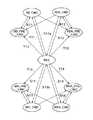
I.行コマンド制御シーケンサ103Aの動作
行コマンド制御シーケンサ103Aは、コマンド処理機構102からコマンドを受け取ると、コマンド制御機構105に対してコマンド発行要求111を発行し、コマンド発行許可110を受け取った段階で、コマンド待機状態(以下、IDLE状態と呼ぶ)からコマンドを発行する状態へと遷移する。I. Operation of Row
図4に示すように、行コマンド制御シーケンサ103Aは、アクティブコマンド、プリチャージコマンド、リフレッシュコマンド、オールプリチャージ(Precharge ALL)コマンド、モードセット(ModeSet)コマンド、セルフリフレッシュ(Self Refresh)コマンドを発行する状態に加え、それぞれの状態に遷移する前の前段状態と、列コマンド制御シーケンサ104にコマンドを発行する列コマンド駆動状態(図4中のCOL_START)が存在する。列コマンド駆動状態(COL_START)は、アクティブコマンドを発行する状態から遷移する(図4のM1)。 As shown in FIG. 4, the row
ここで、図4中のACTIVE_STはアクティブコマンドを発行するアクティブ状態を示し、PCHG_STはプリチャージコマンドを発行するプリチャージ状態を示し、REF_STはリフレッシュコマンドを発行するリフレッシュ状態を示し、PALL_STは、オールプリチャージ(Precharge ALL)コマンドを発行するオールプリチャージ状態を示す。また、MDS_STはモードセット(ModeSet)コマンドを発行するモードセット状態を示し、SREF_STはセルフリフレッシュ(Self Refresh)コマンドを発行するセルフリフレッシュ状態を示す。 Here, ACTIVE_ST in FIG. 4 indicates an active state for issuing an active command, PCHG_ST indicates a precharge state for issuing a precharge command, REF_ST indicates a refresh state for issuing a refresh command, and PALL_ST indicates all pre- An all precharge state in which a charge (Precharge ALL) command is issued is shown. MDS_ST indicates a mode set state in which a mode set (ModeSet) command is issued, and SREF_ST indicates a self-refresh state in which a self-refresh (Self Refresh) command is issued.
また、図4中のACTIVE_PREはアクティブコマンドを発行する状態に遷移する前の前段アクティブ状態を示し、PCHG_PREはプリチャージコマンドを発行する状態に遷移する前の前段プリチャージ状態を示し、REF_PREはリフレッシュコマンドを発行する状態に遷移する前の前段リフレッシュ状態を示し、PALL_PREは、オールプリチャージ(Precharge ALL)コマンドを発行する状態に遷移する前の前段オールプリチャージ状態を示す。また、MDS_PREはモードセット(ModeSet)コマンドを発行する状態に遷移する前の前段モードセット状態を示し、SREF_PREはセルフリフレッシュ(Self Refresh)コマンドを発行する状態に遷移する前の前段セルフリフレッシュ状態を示す。 Also, ACTIVE_PRE in FIG. 4 indicates a previous active state before transition to a state for issuing an active command, PCHG_PRE indicates a previous precharge state before transition to a state for issuing a precharge command, and REF_PRE indicates a refresh command. The pre-refresh state before the transition to the state for issuing the pre-charge is issued, and PALL_PRE indicates the pre-stage all pre-charge state before the transition to the state for issuing the all pre-charge (Precharge ALL) command. MDS_PRE indicates the previous mode set state before the transition to the state for issuing the mode set (ModeSet) command, and SREF_PRE indicates the previous stage self-refresh state before the transition to the state for issuing the self-refresh (Self Refresh) command. .
なお、オールプリチャージコマンドは、メモリデバイス201における全バンクの一括プリチャージを指示するコマンドであり、モードセットコマンドは、モードレジスタにモードパラメータの供給を指示するコマンドであり、セルフリフレッシュコマンドは、SDRAMから成るメモリデバイス201の内部でリフレッシュサイクルを実行するためのセルフリフレッシュ動作を指示するコマンドである。 The all precharge command is a command for instructing batch precharge of all banks in the
各コマンドを発行する状態では、行コマンド駆動信号116と、それぞれのコマンドで必要とするCS信号117、RAS信号112、CAS信号113、WE信号114及びアドレス115とをコマンド制御機構105に対して駆動するように制御される。 In the state in which each command is issued, the
これに対して、それぞれの状態に遷移する前の前段状態では、行コマンド駆動信号116と、それぞれのコマンドで必要とするRAS信号112、CAS信号113、WE信号114及びアドレス115とをコマンド制御機構105に対して駆動するように制御される。 On the other hand, in the previous stage state before the transition to each state, the command control mechanism transmits the row
IDLE状態から、各コマンドを発行する状態あるいは各状態へ遷移する前の前段状態へ遷移の選択は、デコーダ103−1による負荷レベルの判定に基づいて行われる。負荷レベルが小さいと判定された場合は、IDLE状態から直接各コマンドを発行する状態へと遷移(図4中のS1〜S6参照)するのに対して、負荷レベルが大きいと判定された場合は、IDLE状態から前段状態へと遷移(図4中のT1〜T5参照)が行われた後に、各コマンドを発行する状態へと遷移(図4中のN1〜N5参照)が行われる。 Selection of transition from the IDLE state to a state in which each command is issued or a previous state before transitioning to each state is performed based on determination of a load level by the decoder 103-1. When it is determined that the load level is low, the state transitions directly from the IDLE state to a state where each command is issued (see S1 to S6 in FIG. 4), whereas when it is determined that the load level is high After the transition from the IDLE state to the previous state (see T1 to T5 in FIG. 4), the transition to the state in which each command is issued (see N1 to N5 in FIG. 4) is performed.
各前段状態では、RAS信号125、CAS信号126、WE信号127及びアドレス128が駆動状態となり、各コマンドを発行する状態では、前記の信号群に加え、CS信号130が駆動状態となる。 In each preceding state, the
次に、このような行コマンド制御シーケンサ103Aの動作について、リフレッシュコマンド及びアクティブコマンドの発行を例に説明する。 Next, the operation of the row
まずリフレッシュ動作について説明すると、リフレッシュコマンドは、CS信号130、RAS信号125、CAS信号126及びアドレス128を駆動する必要がある。リフレッシュコマンドの発行時はIDLE状態であり、コマンド制御機構105からコマンド発行許可110を受け取った状態で状態遷移が行われる。 First, the refresh operation will be described. The refresh command needs to drive the
負荷レベルが小さいと判定された場合は、IDLE状態からリフレッシュ状態(REF_ST)へと遷移が行われ(図4のS4)、リフレッシュ状態では、行アドレス駆動信号116、CS信号117、RAS信号112、CAS信号113及びアドレス115が駆動され、次のサイクルにおいてIDLE状態へと遷移する(図4のS4a)。一方、負荷レベルが大きいと判定された場合は、IDLE状態から一旦前段リフレッシュ状態(REF_PRE)へと遷移が行われ(図4のT3)、前段リフレッシュ状態では、行アドレス駆動信号116、RAS信号112、CAS信号113及びアドレス115が駆動される。次のサイクルにおいてはリフレッシュ状態へと遷移が行われ(図4のN3)、行アドレス駆動信号116、CS信号117、RAS信号112、CAS信号113及びアドレス115が駆動され、さらに次のサイクルによってIDLE状態へと遷移する(図4のS4a)。 When it is determined that the load level is low, a transition is made from the IDLE state to the refresh state (REF_ST) (S4 in FIG. 4). In the refresh state, the row
以上により、負荷レベルが小さいと判定された場合には、コマンド制御機構105では、CS信号130、RAS信号125、CAS信号126及びアドレス128をそれぞれ1サイクル間に亘ってメモリデバイス201に対して駆動し(図6のW1を参照)、負荷レベルが大きいと判定された場合には、RAS信号125、CAS信号126及びアドレス128をそれぞれ2サイクル間に亘って駆動し(図7のY1を参照)、CS信号130は最後の1サイクル間のみ駆動するように、制御が行われる。 As described above, when it is determined that the load level is low, the
続いて、アクティブ動作について説明すると、アクティブコマンドは、CS信号130、RAS信号125及びアドレス128を駆動する必要がある。アクティブコマンドの発行時はIDLE状態であり、コマンド制御機構105よりコマンド発行許可110を受け取った段階で状態遷移が行われる。 Subsequently, the active operation will be described. The active command needs to drive the
負荷レベルが小さいと判定された場合は、IDLE状態からアクティブ状態(ACTIVE_ST)へと遷移が行われる(図4のS2)。アクティブ状態では、行アドレス駆動信号116、CS信号117、RAS信号112及びアドレス115が駆動され、列コマンド駆動状態(COL_START)へと遷移し(図4のM1)、列コマンド制御シーケンサ104を駆動し、後続のアクセスが無い場合はIDLE状態へと遷移する(図4のM2)。 When it is determined that the load level is low, a transition is made from the IDLE state to the active state (ACTIVE_ST) (S2 in FIG. 4). In the active state, the row
負荷レベルが大きいと判定された場合は、IDLE状態から一旦前段アクティブ状態(ACTIVE_PRE)へと遷移が行われ(図4のT2)、前段アクティブ状態では行アドレス駆動信号116、RAS信号112及びアドレス115が駆動される。次のサイクルにおいてはアクティブ状態(ACTIVE_ST)へと遷移が行われ(図4のN2)、行アドレス駆動信号116、CS信号117、RAS信号112及びアドレス115が駆動され、列コマンド駆動状態(COL_START)へと遷移し(図4のM1)、列コマンド制御シーケンサ104を駆動し、後続のアクセスが無い場合はIDLE状態へと遷移する(図4のM2)。 If it is determined that the load level is high, a transition is made from the IDLE state to the previous active state (ACTIVE_PRE) (T2 in FIG. 4). In the previous active state, the row
以上より、負荷レベルが小さいと判定された場合には、コマンド制御機構105では、CS信号130、RAS信号125及びアドレス128を1サイクル間に亘ってメモリデバイス201に対して駆動し(図6のW2を参照)、負荷レベルが大きいと判定された場合には、RAS信号125及びアドレス128を2サイクル間に亘って駆動し(図7のY2)、CS信号130は最後の1サイクル間のみ駆動するように、制御が行われる。 As described above, when it is determined that the load level is low, the
II.列コマンド制御シーケンサ104Aの動作
列コマンド制御シーケンサ104Aは、行コマンド制御シーケンサ103Aよりコマンドを受け取るとコマンド制御機構105に対してコマンド発行要求119を発行し、コマンド発行許可118を受け取った段階で、IDLE状態からコマンドを発行する状態へと遷移が行われる。II. Operation of the Column
図5に示すように、列コマンド制御シーケンサ104Aは、ライトコマンド、プリチャージ・ライトコマンド(Write with Precharge)、リードコマンド、プリチャージ・リードコマンド(Read with Precharge)を発行する状態に加え、それぞれの状態に遷移する前の前段状態が存在する。 As shown in FIG. 5, the column
ここで、プリチャージ・ライトコマンドとは、ビット線をプリチャージしてデータを書き込むためのコマンドであり、プリチャージ・リードコマンドとは、ビット線をプリチャージしてデータを読み出すためのコマンドである。 Here, the precharge / write command is a command for precharging the bit line and writing data, and the precharge / read command is a command for precharging the bit line and reading data. .
また、図5中のRD_CMDはリードコマンドを発行するリード状態を示し、RDA_CMDはプリチャージ・リードコマンドを発行するプリチャージ・リード状態を示し、WR_CMDはライトコマンドを発行するライト状態を示し、WRA_CMDはプリチャージ・ライトコマンドを発行するプリチャージ・ライト状態を示す。RD_PREはリードコマンドを発行する状態に遷移する前の前段リード状態を示し、RDA_PREはプリチャージ・リードコマンドを発行する状態に遷移する前の前段プリチャージ・リード状態を示し、WR_PREはライトコマンドを発行する状態に遷移する前の前段ライト状態を示し、WRA_PREはプリチャージ・ライトコマンドを発行する状態に遷移する前の前段プリチャージ・ライト状態を示す。 In FIG. 5, RD_CMD indicates a read state for issuing a read command, RDA_CMD indicates a precharge / read state for issuing a precharge / read command, WR_CMD indicates a write state for issuing a write command, and WRA_CMD indicates Indicates a precharge / write state in which a precharge / write command is issued. RD_PRE indicates the previous stage read state before the transition to the state for issuing the read command, RDA_PRE indicates the previous stage precharge / read state before the transition to the state for issuing the precharge / read command, and WR_PRE issues the write command. WRA_PRE indicates a pre-stage precharge / write state before transition to a state in which a precharge / write command is issued.
各コマンドを発行する状態では、列コマンド駆動信号123と、それぞれのコマンドで必要とするCS信号124、CAS信号120、WE信号121及びアドレス122とをコマンド制御機構105に対して駆動するように制御される。これに対して、それぞれの状態に遷移する前の前段状態では、列コマンド駆動信号123と、それぞれのコマンドで必要とするCAS信号120、WE信号121及びアドレス122とをコマンド制御機構105に対して駆動するように制御される。 In a state in which each command is issued, control is performed so that the column
IDLE状態から、各コマンドを発行する状態、あるいは各状態へ遷移する前の前段状態へ遷移の選択は、デコーダ104−1による負荷レベル判定に基づいて行われる。負荷レベルが小さいと判定された場合は、IDLE状態から直接各コマンドを発行する状態へと遷移(図5中のS11〜S14参照)するのに対して、負荷レベルが大きいと判定された場合は、IDLE状態から前段状態へと遷移(図5中のT11〜T14参照)が行われた後に、コマンドを発行する状態へと遷移(図5中のN11〜N14参照)が行われる。 Selection of the transition from the IDLE state to the state in which each command is issued or the previous state before transitioning to each state is performed based on the load level determination by the decoder 104-1. When it is determined that the load level is low, the state transitions directly from the IDLE state to a state in which each command is issued (see S11 to S14 in FIG. 5), whereas when it is determined that the load level is high. After the transition from the IDLE state to the previous state (see T11 to T14 in FIG. 5), the transition to the state in which the command is issued (see N11 to N14 in FIG. 5) is performed.
各前段状態では、CAS信号126、WE信号127及びアドレス128が駆動状態となり、各コマンドを発行する状態では、前記の信号群に加えてCS信号130が駆動状態となる。 In each preceding state, the
次に、このような列コマンド制御シーケンサ104Aの動作について、ライトコマンド及びリードコマンドの発行を例に説明する。 Next, the operation of the column
まず、ライトコマンドの発行について説明すると、ライトコマンドは、CS信号130、CAS信号126、WE信号127及びアドレス128を駆動する必要がある。ライトコマンドの発行時はIDLE状態であり、コマンド制御機構105よりコマンド発行許可118を受け取った状態で状態遷移が行われる。 First, the issue of a write command will be described. The write command needs to drive the
負荷レベルが小さいと判定された場合は、IDLE状態からライト状態へと遷移が行われ(図5のS13)、ライト状態では列アドレス駆動信号123、CS信号124、CAS信号120、WE信号121及びアドレス122が駆動され、後続のアクセスが無い場合はIDLE状態へと遷移する(図5のS13a)。一方、負荷レベルが大きいと判定された場合は、IDLE状態から一旦前段ライト状態へと遷移が行われ(図5のT13)、前段ライト状態では列アドレス駆動信号123、CAS信号120、WE信号121及びアドレス122が駆動される。次のサイクルにおいてはライト状態へと遷移が行われ(図5のN13)、列アドレス駆動信号123、CS信号124、CAS信号120、WE信号121及びアドレス122が駆動され、後続のアクセスが無い場合はIDLE状態へと遷移する(図5のS13a)。 If it is determined that the load level is low, a transition is made from the IDLE state to the write state (S13 in FIG. 5). In the write state, the column
以上より、負荷レベルが小さいと判定された場合は、CS信号124、CAS信号120、WE信号121及びアドレス122をそれぞれ1サイクル間に亘ってメモリデバイス201に対して駆動し(図6のW3)、負荷レベルが大きいと判定された場合は、CAS信号120、WE信号121及びアドレス122を2サイクル間に亘って駆動し(図7のY3)、CS信号130は最後の1サイクル間のみ駆動するように、制御が行われる。 As described above, when it is determined that the load level is low, the
また、ライト状態においては、データ制御機構106に対して出力データタイミング信号108を発行し、データ制御機構106は指定されたタイミングに従いデータをメモリデータバス129へ出力する。 In the write state, the output
続いて、リードコマンド動作について説明する。リードコマンドは、CS信号124、CAS信号120及びアドレス122を駆動する必要がある。リードコマンドの発行時はIDLE状態であり、コマンド制御機構105よりコマンド発行許可118を受け取った状態で状態遷移が行われる。 Next, the read command operation will be described. The read command needs to drive the
負荷レベルが小さいと判定された場合は、IDLE状態からリード状態へと遷移(図5のS11)が行われ、リード状態では列アドレス駆動信号123、CS信号124、CAS信号120及びアドレス122が駆動され、後続のアクセスが無い場合はIDLE状態へと遷移する(図5のS11a)。一方、負荷レベルが大きいと判定された場合は、IDLE状態から一旦前段リード状態へと遷移が行われ(図5のT11)、前段リード状態では列アドレス駆動信号123、CAS信号120及びアドレス122が駆動される。次のサイクルにおいてはリード状態へと遷移が行われ(図5のN11)、列アドレス駆動信号123、CS信号124、CAS信号120及びアドレス122が駆動され、後続のアクセスが無い場合はIDLE状態へと遷移する(図5のS11a)。 If it is determined that the load level is low, a transition is made from the IDLE state to the read state (S11 in FIG. 5), and the column
以上より、負荷レベルが小さいと判定された場合は、CS信号124、CAS信号120及びアドレス122をそれぞれ1サイクル間に亘ってメモリデバイス201に対して駆動し(図6のW4)、負荷レベルが大きいと判定された場合は、CAS信号120及びアドレス122をそれぞれ2サイクル間に亘って駆動し(図7のY4)、CS信号124は最後の1サイクル間のみ駆動するように、制御が行われる。 As described above, when it is determined that the load level is low, the
また、リード状態においては、データ制御機構106に対して入力データタイミング信号109を発行し、データ制御機構106は指定されたタイミングに従いデータをメモリデータバス129から取り込み、コマンド処理機構102に読み込みデータを返す。 In the read state, the input
このように本実施の形態では、CS信号、データ及びデータマスク等の負荷の小さい選択信号/データ系は、常に1サイクル間に亘って駆動し、RAS信号、CAS信号、WE信号及びアドレス等のデータ負荷の大きいコマンド/アドレス系信号は、メモリデバイス個数による負荷の大小判定により1サイクル駆動と2サイクル駆動に切り替えられる。すなわち、負荷の大きなコマンド/アドレス系の信号を2サイクルで駆動するように切替可能にして該コマンド/アドレス系信号が変化する周波数を低くするようにしたので、多くのメモリデバイスを接続した場合であっても、コマンド/アドレス系の信号と選択/データ系信号との負荷の差を吸収することが可能となり、高価なメモリモジュールを用いなくとも、それと等価なシステムを実現することが可能である。また、切替機構を有することで、メモリデバイスの接続個数に最適なシステム環境を構築することができる。 As described above, in the present embodiment, the selection signal / data system having a small load such as the CS signal, data, and data mask is always driven for one cycle, and the RAS signal, CAS signal, WE signal, address, etc. A command / address system signal with a large data load can be switched between a one-cycle drive and a two-cycle drive according to the load determination based on the number of memory devices. That is, the command / address system signal with a large load can be switched to be driven in two cycles so that the frequency at which the command / address system signal changes is lowered, so that when many memory devices are connected. Even in this case, it is possible to absorb the difference in load between the command / address system signal and the selection / data system signal, and it is possible to realize an equivalent system without using an expensive memory module. . Further, by having the switching mechanism, it is possible to construct a system environment that is optimal for the number of memory devices connected.
[第2の実施の形態]
第2の実施の形態は、メモリデバイス201の個数の判定をスイッチ回路ではなくソフトウェアにより行い、さらに1サイクル駆動と2サイクル駆動に切り替えをソフトウェアによって行うようにしたものである。[Second Embodiment]
In the second embodiment, determination of the number of
図8は、本発明の第2の実施の形態に係るメモリコントローラの構成を示すブロック図である。 FIG. 8 is a block diagram showing the configuration of the memory controller according to the second embodiment of the present invention.
本実施の形態のメモリコントローラ200は、内部に負荷の大小レベルを指定するレジスタ150を有し、負荷の大きい場合にはレジスタ150をセットし、負荷が少ない場合はレジスタ150をクリアすることで、コマンドを発行するサイクルを制御するようになっている。その他の構成は、上記第1の実施の形態と同様である。 The
DIMMモジュール等では、EEPROMに保持されるDIMMモジュール情報を有しており、ソフトウェアは、DIMMモジュールのEEPROMにアクセスすることでメモリデバイスの接続個数を知ることができる。また、ソフトウェアが、メモリデバイスの接続個数により負荷の大小を判定してレジスタ150を設定することで、コマンドの発行サイクルを変更することができる。 The DIMM module or the like has DIMM module information held in the EEPROM, and the software can know the number of connected memory devices by accessing the EEPROM of the DIMM module. In addition, the software can determine the load level based on the number of connected memory devices and set the
その際、レジスタ150の初期値として負荷が大きいことを指定し、メモリデバイス201の初期化時は2サイクル間に亘ってコマンドを発行し、負荷が小さいと判定された場合にはレジスタ150をクリアすることで、コマンドの発行サイクルを変更する。 At that time, it is specified that the load is large as the initial value of the
なお、本発明は、上記各実施の形態に限定されるものではなく、その主旨を逸脱しない限り種々の変更が可能である。例えば、メモリコントローラ200の構成は、負荷レベルに基づいてコマンド/アドレス系信号の出力サイクル数を変更できること以外は任意の構成で実現可能である。 In addition, this invention is not limited to said each embodiment, A various change is possible unless it deviates from the main point. For example, the configuration of the
本発明は、上述した実施形態の装置に限定されず、複数の機器から構成されるシステムに適用しても、1つの機器から成る装置に適用しても良い。前述した実施形態の機能を実現するソフトウェアのプログラムコードを記憶した記憶媒体をシステムあるいは装置に供給し、そのシステムあるいは装置のコンピュータ(又はCPUやMPU)が記憶媒体に格納されたプログラムコードを読み出し実行することによっても、完成されることは言うまでもない。 The present invention is not limited to the apparatus of the above-described embodiment, and may be applied to a system composed of a plurality of devices or an apparatus composed of one device. A storage medium storing software program codes for realizing the functions of the above-described embodiments is supplied to a system or apparatus, and a computer (or CPU or MPU) of the system or apparatus reads and executes the program codes stored in the storage medium. Needless to say, it will be completed by doing.
この場合、記憶媒体から読み出されたプログラムコード自体が前述した実施形態の機能を実現することになり、そのプログラムコードを記憶した記憶媒体は本発明を構成することになる。プログラムコードを供給するための記憶媒体としては、例えば、フロッピー(登録商標)ディスク、ハードディスク、光ディスク、光磁気ディスク、CD−不揮発性メモリ、CD−R、磁気テープ、不揮発性のメモリカード、不揮発性メモリを用いることができる。また、コンピュータが読み出したプログラムコードを実行することにより、前述した実施形態の機能が実現されるだけではなく、そのプログラムコードの指示に基づき、コンピュータ上で稼動しているOSなどが実際の処理の一部又は全部を行い、その処理によって前述した実施形態の機能が実現される場合も含まれることは言うまでもない。 In this case, the program code itself read from the storage medium realizes the functions of the above-described embodiments, and the storage medium storing the program code constitutes the present invention. Examples of the storage medium for supplying the program code include a floppy (registered trademark) disk, a hard disk, an optical disk, a magneto-optical disk, a CD-nonvolatile memory, a CD-R, a magnetic tape, a nonvolatile memory card, and a nonvolatile memory card. A memory can be used. In addition, by executing the program code read by the computer, not only the functions of the above-described embodiments are realized, but also the OS running on the computer based on the instruction of the program code performs the actual processing. It goes without saying that a case where the functions of the above-described embodiment are realized by performing part or all of the processing, is also included.
さらに、記憶媒体から読み出されたプログラムコードが、コンピュータに挿入された機能拡張ボードやコンピュータに接続された機能拡張ユニットに備わるメモリに書き込まれた後、次のプログラムコードの指示に基づき、その拡張機能を拡張ボードや拡張ユニットに備わるCPUなどが処理を行って実際の処理の一部又は全部を行い、その処理によって前述した実施形態の機能が実現される場合も含まれることは言うまでもない。 Furthermore, after the program code read from the storage medium is written to the memory provided in the function expansion board inserted in the computer or the function expansion unit connected to the computer, the program code is expanded based on the instruction of the next program code. It goes without saying that the functions of the embodiment described above are realized by performing some or all of the actual processing by the CPU or the like provided on the expansion board or expansion unit.
102 コマンド処理機構
103A 行コマンド制御シーケンサ
104A 列コマンド制御シーケンサ
105 コマンド制御機構
106 データ制御機構
125 RAS信号
126 CAS信号
127 WE信号
128 アドレス
129 データ信号
200 メモリコントローラ
201 メモリデバイス
203 デバイス個数切替スイッチ102
Claims (8)
Translated fromJapanese前記状態遷移に基づいて、前記メモリデバイスに対するアクセス動作を行う手段とを備えたことを特徴とするメモリアクセス制御装置。Based on load information corresponding to the number of connected memory devices, means for changing the state transition of command processing;
Means for performing an access operation on the memory device based on the state transition.
前記メモリデバイスの接続個数を通知する通知手段と、
前記通知手段の通知結果に対応して負荷の大小を判定する判定手段とを備え、
前記負荷の大小に応じて、前記コマンド/アドレス系信号の発行サイクルを変更したことを特徴とする情報処理システム。A memory access control device configured to be able to change a command / address system signal issue cycle for controlling access to a memory device;
Notification means for notifying the number of connected memory devices;
Determination means for determining the magnitude of the load in response to the notification result of the notification means,
An information processing system, wherein the command / address system signal issue cycle is changed in accordance with the magnitude of the load.
前記メモリデバイスの接続個数を通知する通知手段を設け、
前記メモリアクセス制御装置は、
前記コマンド/アドレス系信号の発行サイクル数を切り替え可能に構成したコマンドサイクル制御手段と、
前記通知手段の通知結果に対応して負荷の大小を判定する判定手段と、
前記判定手段により負荷が大きいと判定された場合は前記コマンド/アドレス系信号の発行サイクル数を多くし、負荷が小さいと判定された場合は前記コマンド/アドレス系信号のクロックサイクル数を少なくするように前記コマンドサイクル制御手段に指示するコマンドサイクル指定手段とを有することを特徴とする情報処理システム。In an information processing system having a memory access control device for controlling access to a memory device by a command / address system signal,
Providing a notification means for notifying the number of connected memory devices;
The memory access control device includes:
Command cycle control means configured to switch the number of issuing cycles of the command / address system signal;
Determination means for determining the magnitude of the load in response to the notification result of the notification means;
If the determination unit determines that the load is large, the command / address system signal issuance cycle number is increased, and if the load is determined to be small, the command / address system signal clock cycle number is decreased. And a command cycle designating means for instructing the command cycle control means.
前記状態遷移に基づいて、前記メモリデバイスに対するアクセス動作を行う工程とを備えたことを特徴とするメモリアクセス制御方法。Changing the command processing state transition based on load information corresponding to the number of connected memory devices;
And a step of performing an access operation to the memory device based on the state transition.
前記メモリデバイスの接続個数に対応した負荷情報に基づいて、コマンド処理の状態遷移を変化させるステップと、
前記状態遷移に基づいて、前記メモリデバイスに対するアクセス動作を行うステップとを備えたことを特徴とする制御プログラム。A control program for executing a control method of a memory access control device for controlling access to a memory device,
Changing the command processing state transition based on load information corresponding to the number of connected memory devices;
And a step of performing an access operation to the memory device based on the state transition.
Priority Applications (2)
| Application Number | Priority Date | Filing Date | Title |
|---|---|---|---|
| JP2004166339AJP2005346502A (en) | 2004-06-03 | 2004-06-03 | Memory access control device, information processing system, memory access control method, and control program |
| US11/143,825US7536519B2 (en) | 2004-06-03 | 2005-06-02 | Memory access control apparatus and method for accomodating effects of signal delays caused by load |
Applications Claiming Priority (1)
| Application Number | Priority Date | Filing Date | Title |
|---|---|---|---|
| JP2004166339AJP2005346502A (en) | 2004-06-03 | 2004-06-03 | Memory access control device, information processing system, memory access control method, and control program |
Publications (1)
| Publication Number | Publication Date |
|---|---|
| JP2005346502Atrue JP2005346502A (en) | 2005-12-15 |
Family
ID=35450286
Family Applications (1)
| Application Number | Title | Priority Date | Filing Date |
|---|---|---|---|
| JP2004166339AWithdrawnJP2005346502A (en) | 2004-06-03 | 2004-06-03 | Memory access control device, information processing system, memory access control method, and control program |
Country Status (2)
| Country | Link |
|---|---|
| US (1) | US7536519B2 (en) |
| JP (1) | JP2005346502A (en) |
Families Citing this family (5)
| Publication number | Priority date | Publication date | Assignee | Title |
|---|---|---|---|---|
| JP5517830B2 (en)* | 2010-08-19 | 2014-06-11 | ルネサスエレクトロニクス株式会社 | Semiconductor integrated circuit |
| JP2012174184A (en)* | 2011-02-24 | 2012-09-10 | Canon Inc | Information processing device and control method of information processing device |
| JP7197998B2 (en)* | 2018-05-02 | 2022-12-28 | キヤノン株式会社 | Memory controllers and methods implemented in memory controllers |
| US11544203B2 (en)* | 2019-12-30 | 2023-01-03 | Micron Technology, Inc. | Sequencer chaining circuitry |
| JP7431791B2 (en)* | 2021-12-01 | 2024-02-15 | 株式会社日立製作所 | Storage system and data processing method |
Family Cites Families (7)
| Publication number | Priority date | Publication date | Assignee | Title |
|---|---|---|---|---|
| US5577236A (en)* | 1994-12-30 | 1996-11-19 | International Business Machines Corporation | Memory controller for reading data from synchronous RAM |
| JPH08321761A (en) | 1995-05-24 | 1996-12-03 | Nec Eng Ltd | Output buffer circuit |
| US6154821A (en)* | 1998-03-10 | 2000-11-28 | Rambus Inc. | Method and apparatus for initializing dynamic random access memory (DRAM) devices by levelizing a read domain |
| US6496911B1 (en)* | 1998-10-02 | 2002-12-17 | International Business Machines Corporation | Apparatus for memory bus tuning and methods therefor |
| US6981089B2 (en)* | 2001-12-31 | 2005-12-27 | Intel Corporation | Memory bus termination with memory unit having termination control |
| JP3804832B2 (en) | 2002-05-23 | 2006-08-02 | 日本電気株式会社 | Memory device and computer system |
| US8250330B2 (en)* | 2004-12-11 | 2012-08-21 | International Business Machines Corporation | Memory controller having tables mapping memory addresses to memory modules |
- 2004
- 2004-06-03JPJP2004166339Apatent/JP2005346502A/ennot_activeWithdrawn
- 2005
- 2005-06-02USUS11/143,825patent/US7536519B2/ennot_activeExpired - Fee Related
Also Published As
| Publication number | Publication date |
|---|---|
| US7536519B2 (en) | 2009-05-19 |
| US20050273566A1 (en) | 2005-12-08 |
Similar Documents
| Publication | Publication Date | Title |
|---|---|---|
| US6781911B2 (en) | Early power-down digital memory device and method | |
| US5999472A (en) | Multi-bank synchronous semiconductor memory device with easy control | |
| US5471430A (en) | Test circuit for refresh counter of clock synchronous type semiconductor memory device | |
| KR100618070B1 (en) | Dynamic memory circuit with automatic refresh function | |
| KR100518397B1 (en) | Semiconductor memory device and control method | |
| KR100233973B1 (en) | Synchronous semiconductor memory device having internal circuitry enabled only when commands are applied in normal sequence | |
| CN100495568C (en) | Method for accessing data and device and system using the method | |
| US6192446B1 (en) | Memory device with command buffer | |
| JP2008108417A (en) | Low power dram and its driving method | |
| US6166973A (en) | Memory device with multiple-bit data pre-fetch function | |
| JP2000030456A (en) | Memory device | |
| US20050071541A1 (en) | Method and apparatus for implicit DRAM precharge | |
| US9030895B2 (en) | Memory device with pin register to set input/output direction and bitwidth of data signals | |
| JPH10162576A (en) | Column select line enable circuit for semiconductor memory device | |
| US20020136079A1 (en) | Semiconductor memory device and information processing system | |
| JP4744777B2 (en) | Semiconductor memory device having divided cell array and memory cell access method of the device | |
| JPH10208468A (en) | Semiconductor storage device and synchronous semiconductor storage device | |
| EP1600980A1 (en) | Semiconductor memory device without decreasing performance thereof even if refresh operation or word line changing operation occur during burst operation | |
| US6411563B1 (en) | Semiconductor integrated circuit device provided with a logic circuit and a memory circuit and being capable of efficient interface between the same | |
| US7239569B2 (en) | Semiconductor memory device and memory system | |
| JP2000163962A (en) | Clock synchronization system | |
| JP2005346502A (en) | Memory access control device, information processing system, memory access control method, and control program | |
| US6885603B2 (en) | Dynamic random access memory devices and method of controlling refresh operation thereof | |
| JP4060527B2 (en) | Clock synchronous dynamic memory | |
| JPH09237492A (en) | Memory controller |
Legal Events
| Date | Code | Title | Description |
|---|---|---|---|
| RD03 | Notification of appointment of power of attorney | Free format text:JAPANESE INTERMEDIATE CODE: A7423 Effective date:20060419 | |
| A300 | Application deemed to be withdrawn because no request for examination was validly filed | Free format text:JAPANESE INTERMEDIATE CODE: A300 Effective date:20070807 |