JP2005309150A - Electronic circuit, driving method thereof, electro-optical device, and electronic apparatus - Google Patents
Electronic circuit, driving method thereof, electro-optical device, and electronic apparatusDownload PDFInfo
- Publication number
- JP2005309150A JP2005309150AJP2004126931AJP2004126931AJP2005309150AJP 2005309150 AJP2005309150 AJP 2005309150AJP 2004126931 AJP2004126931 AJP 2004126931AJP 2004126931 AJP2004126931 AJP 2004126931AJP 2005309150 AJP2005309150 AJP 2005309150A
- Authority
- JP
- Japan
- Prior art keywords
- period
- voltage
- current
- driving transistor
- turned
- Prior art date
- Legal status (The legal status is an assumption and is not a legal conclusion. Google has not performed a legal analysis and makes no representation as to the accuracy of the status listed.)
- Granted
Links
- 238000000034methodMethods0.000titleclaimsdescription20
- 239000003990capacitorSubstances0.000claimsdescription21
- 230000008859changeEffects0.000abstractdescription14
- 238000010586diagramMethods0.000description9
- 230000006870functionEffects0.000description9
- 239000010408filmSubstances0.000description4
- 239000011159matrix materialSubstances0.000description4
- 238000003384imaging methodMethods0.000description3
- 230000003287optical effectEffects0.000description3
- 230000003071parasitic effectEffects0.000description3
- 239000004973liquid crystal related substanceSubstances0.000description2
- 239000000758substrateSubstances0.000description2
- WHXSMMKQMYFTQS-UHFFFAOYSA-NLithiumChemical compound[Li]WHXSMMKQMYFTQS-UHFFFAOYSA-N0.000description1
- 229910052782aluminiumInorganic materials0.000description1
- XAGFODPZIPBFFR-UHFFFAOYSA-NaluminiumChemical compound[Al]XAGFODPZIPBFFR-UHFFFAOYSA-N0.000description1
- 230000005540biological transmissionEffects0.000description1
- 238000004891communicationMethods0.000description1
- 230000000295complement effectEffects0.000description1
- 230000000694effectsEffects0.000description1
- 238000005401electroluminescenceMethods0.000description1
- 239000011521glassSubstances0.000description1
- 230000006872improvementEffects0.000description1
- 239000012535impuritySubstances0.000description1
- AMGQUBHHOARCQH-UHFFFAOYSA-Nindium;oxotinChemical compound[In].[Sn]=OAMGQUBHHOARCQH-UHFFFAOYSA-N0.000description1
- PNDPGZBMCMUPRI-UHFFFAOYSA-NiodineChemical compoundIIPNDPGZBMCMUPRI-UHFFFAOYSA-N0.000description1
- 230000001678irradiating effectEffects0.000description1
- 229910052744lithiumInorganic materials0.000description1
- 230000007257malfunctionEffects0.000description1
- 229910052751metalInorganic materials0.000description1
- 239000002184metalSubstances0.000description1
- 239000000203mixtureSubstances0.000description1
- 238000012986modificationMethods0.000description1
- 230000004048modificationEffects0.000description1
- 229910021420polycrystalline siliconInorganic materials0.000description1
- 229920000642polymerPolymers0.000description1
- 229920005591polysiliconPolymers0.000description1
- 230000008569processEffects0.000description1
- 230000004044responseEffects0.000description1
- GGCZERPQGJTIQP-UHFFFAOYSA-Nsodium;9,10-dioxoanthracene-2-sulfonic acidChemical compound[Na+].C1=CC=C2C(=O)C3=CC(S(=O)(=O)O)=CC=C3C(=O)C2=C1GGCZERPQGJTIQP-UHFFFAOYSA-N0.000description1
- 230000001360synchronised effectEffects0.000description1
- 239000010409thin filmSubstances0.000description1
Images


Classifications
- G—PHYSICS
- G09—EDUCATION; CRYPTOGRAPHY; DISPLAY; ADVERTISING; SEALS
- G09G—ARRANGEMENTS OR CIRCUITS FOR CONTROL OF INDICATING DEVICES USING STATIC MEANS TO PRESENT VARIABLE INFORMATION
- G09G3/00—Control arrangements or circuits, of interest only in connection with visual indicators other than cathode-ray tubes
- G09G3/20—Control arrangements or circuits, of interest only in connection with visual indicators other than cathode-ray tubes for presentation of an assembly of a number of characters, e.g. a page, by composing the assembly by combination of individual elements arranged in a matrix no fixed position being assigned to or needed to be assigned to the individual characters or partial characters
- G09G3/22—Control arrangements or circuits, of interest only in connection with visual indicators other than cathode-ray tubes for presentation of an assembly of a number of characters, e.g. a page, by composing the assembly by combination of individual elements arranged in a matrix no fixed position being assigned to or needed to be assigned to the individual characters or partial characters using controlled light sources
- G09G3/30—Control arrangements or circuits, of interest only in connection with visual indicators other than cathode-ray tubes for presentation of an assembly of a number of characters, e.g. a page, by composing the assembly by combination of individual elements arranged in a matrix no fixed position being assigned to or needed to be assigned to the individual characters or partial characters using controlled light sources using electroluminescent panels
- G09G3/32—Control arrangements or circuits, of interest only in connection with visual indicators other than cathode-ray tubes for presentation of an assembly of a number of characters, e.g. a page, by composing the assembly by combination of individual elements arranged in a matrix no fixed position being assigned to or needed to be assigned to the individual characters or partial characters using controlled light sources using electroluminescent panels semiconductive, e.g. using light-emitting diodes [LED]
- G09G3/3208—Control arrangements or circuits, of interest only in connection with visual indicators other than cathode-ray tubes for presentation of an assembly of a number of characters, e.g. a page, by composing the assembly by combination of individual elements arranged in a matrix no fixed position being assigned to or needed to be assigned to the individual characters or partial characters using controlled light sources using electroluminescent panels semiconductive, e.g. using light-emitting diodes [LED] organic, e.g. using organic light-emitting diodes [OLED]
- G09G3/3225—Control arrangements or circuits, of interest only in connection with visual indicators other than cathode-ray tubes for presentation of an assembly of a number of characters, e.g. a page, by composing the assembly by combination of individual elements arranged in a matrix no fixed position being assigned to or needed to be assigned to the individual characters or partial characters using controlled light sources using electroluminescent panels semiconductive, e.g. using light-emitting diodes [LED] organic, e.g. using organic light-emitting diodes [OLED] using an active matrix
- G09G3/3233—Control arrangements or circuits, of interest only in connection with visual indicators other than cathode-ray tubes for presentation of an assembly of a number of characters, e.g. a page, by composing the assembly by combination of individual elements arranged in a matrix no fixed position being assigned to or needed to be assigned to the individual characters or partial characters using controlled light sources using electroluminescent panels semiconductive, e.g. using light-emitting diodes [LED] organic, e.g. using organic light-emitting diodes [OLED] using an active matrix with pixel circuitry controlling the current through the light-emitting element
- G—PHYSICS
- G09—EDUCATION; CRYPTOGRAPHY; DISPLAY; ADVERTISING; SEALS
- G09G—ARRANGEMENTS OR CIRCUITS FOR CONTROL OF INDICATING DEVICES USING STATIC MEANS TO PRESENT VARIABLE INFORMATION
- G09G2300/00—Aspects of the constitution of display devices
- G09G2300/04—Structural and physical details of display devices
- G09G2300/0404—Matrix technologies
- G09G2300/0417—Special arrangements specific to the use of low carrier mobility technology
- G—PHYSICS
- G09—EDUCATION; CRYPTOGRAPHY; DISPLAY; ADVERTISING; SEALS
- G09G—ARRANGEMENTS OR CIRCUITS FOR CONTROL OF INDICATING DEVICES USING STATIC MEANS TO PRESENT VARIABLE INFORMATION
- G09G2300/00—Aspects of the constitution of display devices
- G09G2300/08—Active matrix structure, i.e. with use of active elements, inclusive of non-linear two terminal elements, in the pixels together with light emitting or modulating elements
- G09G2300/0809—Several active elements per pixel in active matrix panels
- G09G2300/0819—Several active elements per pixel in active matrix panels used for counteracting undesired variations, e.g. feedback or autozeroing
- G—PHYSICS
- G09—EDUCATION; CRYPTOGRAPHY; DISPLAY; ADVERTISING; SEALS
- G09G—ARRANGEMENTS OR CIRCUITS FOR CONTROL OF INDICATING DEVICES USING STATIC MEANS TO PRESENT VARIABLE INFORMATION
- G09G2300/00—Aspects of the constitution of display devices
- G09G2300/08—Active matrix structure, i.e. with use of active elements, inclusive of non-linear two terminal elements, in the pixels together with light emitting or modulating elements
- G09G2300/0809—Several active elements per pixel in active matrix panels
- G09G2300/0842—Several active elements per pixel in active matrix panels forming a memory circuit, e.g. a dynamic memory with one capacitor
- G09G2300/0861—Several active elements per pixel in active matrix panels forming a memory circuit, e.g. a dynamic memory with one capacitor with additional control of the display period without amending the charge stored in a pixel memory, e.g. by means of additional select electrodes
- G—PHYSICS
- G09—EDUCATION; CRYPTOGRAPHY; DISPLAY; ADVERTISING; SEALS
- G09G—ARRANGEMENTS OR CIRCUITS FOR CONTROL OF INDICATING DEVICES USING STATIC MEANS TO PRESENT VARIABLE INFORMATION
- G09G2310/00—Command of the display device
- G09G2310/02—Addressing, scanning or driving the display screen or processing steps related thereto
- G09G2310/0243—Details of the generation of driving signals
- G09G2310/0251—Precharge or discharge of pixel before applying new pixel voltage
- G—PHYSICS
- G09—EDUCATION; CRYPTOGRAPHY; DISPLAY; ADVERTISING; SEALS
- G09G—ARRANGEMENTS OR CIRCUITS FOR CONTROL OF INDICATING DEVICES USING STATIC MEANS TO PRESENT VARIABLE INFORMATION
- G09G2320/00—Control of display operating conditions
- G09G2320/02—Improving the quality of display appearance
- G09G2320/0242—Compensation of deficiencies in the appearance of colours
- G—PHYSICS
- G09—EDUCATION; CRYPTOGRAPHY; DISPLAY; ADVERTISING; SEALS
- G09G—ARRANGEMENTS OR CIRCUITS FOR CONTROL OF INDICATING DEVICES USING STATIC MEANS TO PRESENT VARIABLE INFORMATION
- G09G2320/00—Control of display operating conditions
- G09G2320/04—Maintaining the quality of display appearance
- G09G2320/043—Preventing or counteracting the effects of ageing
Landscapes
- Engineering & Computer Science (AREA)
- Physics & Mathematics (AREA)
- Computer Hardware Design (AREA)
- General Physics & Mathematics (AREA)
- Theoretical Computer Science (AREA)
- Control Of El Displays (AREA)
- Control Of Indicators Other Than Cathode Ray Tubes (AREA)
- Electroluminescent Light Sources (AREA)
Abstract
Translated fromJapaneseDescription
Translated fromJapanese 本発明は、有機発光ダイオード素子のような電流駆動型素子を駆動する電子回路、電子
回路の駆動方法、電気光学装置および電子機器に関する。The present invention relates to an electronic circuit for driving a current-driven element such as an organic light-emitting diode element, a driving method for the electronic circuit, an electro-optical device, and an electronic apparatus.
近年、液晶素子に代わる次世代の発光デバイスとして、有機エレクトロルミネッセンス
素子や発光ポリマー素子などと呼ばれる有機発光ダイオード(Organic Light Emitting D
iode、以下適宜「OLED素子」と略称する)素子が注目されている。このOLED素子
は、自発光型であるために視野角依存性が少なく、また、バックライトや反射光が不要で
あるために低消費電力化や薄型化に向いているなど、表示パネルとして優れた特性を有し
ている。
ここで、OLED素子は、液晶素子のように電圧保持性を有さず、電流が途絶えると、
発光状態が維持できなくなる電流型の被駆動素子である。このため、OLED素子をアク
ティブ・マトリクス方式で駆動する場合、書込期間(選択期間)において、画素の階調に
応じた電圧を駆動トランジスタのゲートに書き込んで、当該電圧をゲート容量などにより
保持し、当該ゲート電圧に応じた電流を駆動トランジスタがOLED素子に流し続ける構
成が一般的となっている。In recent years, organic light-emitting diodes (Organic Light Emitting D), called organic electroluminescence elements and light-emitting polymer elements, are the next-generation light-emitting devices that can replace liquid crystal elements.
Iode (hereinafter abbreviated as “OLED element” where appropriate) is drawing attention. Since this OLED element is a self-luminous type, it has less viewing angle dependence, and since it does not require a backlight or reflected light, it is suitable for low power consumption and thinning. It has characteristics.
Here, the OLED element does not have voltage holding property like the liquid crystal element, and when the current is interrupted,
This is a current-type driven element that cannot maintain the light emission state. Therefore, when an OLED element is driven by an active matrix method, a voltage corresponding to the gradation of the pixel is written to the gate of the driving transistor in the writing period (selection period), and the voltage is held by a gate capacitance or the like. In general, the driving transistor keeps a current corresponding to the gate voltage flowing through the OLED element.
ところで、この構成では、駆動トランジスタのしきい値電圧特性がばらつくことによっ
て、画素毎に、OLED素子の明るさが相違して表示品位が低下する、という問題が指摘
されている。このため、近年では、書込期間において、当該駆動トランジスタをダイオー
ド接続させるとともに、駆動トランジスタからデータ線に定電流を流し、これによって、
当該駆動トランジスタのゲートに、OLED素子に流すべき電流に応じた電圧を書き込む
ようにプログラミングして、駆動トランジスタのしきい値電圧特性のばらつきを補償する
技術が提案されている(例えば、特許文献1および2参照)。
There has been proposed a technique that compensates for variations in threshold voltage characteristics of a drive transistor by programming the gate of the drive transistor so as to write a voltage corresponding to the current to be passed through the OLED element (for example, Patent Document 1). And 2).
しかしながら、この技術では、例えば駆動トランジスタがnチャネル型である場合に、
OLED素子に流すべき電流が小さくなるように設定するとき、書込期間では、当該駆動
トランジスタのゲート電圧が低く、当該駆動トランジスタのソース・ドレイン間の電流が
流れにくい状態となるので、書込期間内に、当該駆動トランジスタのゲートに目的とする
電圧を書き込むことができない、といった問題が新たに指摘された。
本発明は、上述した事情に鑑みてなされたもので、その目的とするところは、駆動トラ
ンジスタのゲートに、被駆動素子に流すべき電流に応じた電圧を迅速に書き込むことが可
能な電子回路、その駆動方法、当該電子回路を用いた電気光学装置、および、電子機器を
提供することにある。However, in this technique, for example, when the driving transistor is an n-channel type,
When the current to be passed through the OLED element is set to be small, the gate voltage of the driving transistor is low in the writing period, and the current between the source and drain of the driving transistor is difficult to flow. In addition, a problem was pointed out that the target voltage could not be written to the gate of the drive transistor.
The present invention has been made in view of the above-described circumstances, and an object thereof is an electronic circuit capable of quickly writing a voltage corresponding to a current to be supplied to a driven element to a gate of a driving transistor, An object is to provide a driving method thereof, an electro-optical device using the electronic circuit, and an electronic apparatus.
上記目的を達成するために本発明に係る電子回路の駆動方法は、被駆動素子に流れる電
流を制御する駆動トランジスタと、前記駆動トランジスタのゲートとドレインとの間をオ
ンまたはオフする第1のスイッチング素子と、一端が前記駆動トランジスタのゲートに接
続された容量素子とを備える電子回路の駆動方法であって、前記容量素子の他端に初期電
圧を印加するとともに、前記第1のスイッチング素子をオンさせた状態にて、前記被駆動
素子に電流を流し、この後、前記電流を遮断するとともに、前記容量素子の他端に対する
初期電圧の印加を解除し、前記第1のスイッチング素子をオフさせる第1のステップと、
前記容量素子の他端に対し、前記被駆動素子に流すべき電流に応じた電圧を印加する第2
のステップと、保持されたゲート電圧にしたがった電流を、前記駆動トランジスタが前記
被駆動素子に流す第3のステップとを備えることを特徴とする。この方法によれば、第1
のステップにおける第1のスイッチング素子のオンオフによって、容量素子の一端および
駆動トランジスタのゲート(ノードA)には、当該駆動トランジスタのしきい値に応じた
電圧が保持される。次に、第2のステップにおいて、容量素子の他端は、被駆動素子に流
すべき電流に応じた電圧の印加によって初期電圧から変化し、この電圧変化に応じた分だ
け、ノードAの電圧も変化して保持される。第3のステップにおいては、変化後における
ノードAの電圧に応じた電流が被駆動素子に流れるが、このとき流れる電流は、駆動トラ
ンジスタのしきい値特性がキャンセルされている。また、第1のステップにおける容量素
子の保持は、被駆動素子に電流を強制的に流すことによって行われるので、時間を要しな
い。さらに、第2のステップでは、被駆動素子に流すべき電流に応じた電圧を容量素子の
他端に印加するのであって、駆動トランジスタのゲートに直接印加しないので、当該電圧
の書き込みに要する時間を短縮化することができる。In order to achieve the above object, a driving method of an electronic circuit according to the present invention includes a driving transistor that controls a current flowing through a driven element, and a first switching that turns on or off between a gate and a drain of the driving transistor. An electronic circuit driving method comprising: an element; and a capacitive element having one end connected to the gate of the driving transistor, wherein an initial voltage is applied to the other end of the capacitive element and the first switching element is turned on. In this state, a current is passed through the driven element, and then the current is interrupted, and the application of the initial voltage to the other end of the capacitive element is released, and the first switching element is turned off. 1 step,
A second voltage is applied to the other end of the capacitive element according to the current to be passed through the driven element.
And a third step in which the driving transistor causes a current according to the held gate voltage to flow to the driven element. According to this method, the first
By turning on and off the first switching element in the step, a voltage corresponding to the threshold value of the driving transistor is held at one end of the capacitor and the gate (node A) of the driving transistor. Next, in the second step, the other end of the capacitive element is changed from the initial voltage by application of a voltage corresponding to the current to be supplied to the driven element, and the voltage of the node A is also increased by the amount corresponding to this voltage change. Change and hold. In the third step, a current corresponding to the voltage of the node A after the change flows to the driven element, and the threshold current characteristic of the driving transistor is canceled for the current flowing at this time. In addition, since the holding of the capacitor element in the first step is performed by forcing a current to flow through the driven element, no time is required. Furthermore, in the second step, a voltage corresponding to the current to be passed through the driven element is applied to the other end of the capacitive element, and is not applied directly to the gate of the driving transistor. It can be shortened.
この駆動方法では、前記第1のステップにおいて、前記第1のスイッチング素子をオン
させるとともに前記被駆動素子に電流を流して、当該電流に応じた電圧を、前記容量素子
の一端および前記駆動トランジスタのゲートに保持させる一方、前記電流を遮断させた後
に、前記第1のスイッチング素子をオフさせて、前記容量素子の一端および前記駆動トラ
ンジスタのゲートに保持された電圧を、前記駆動トランジスタのしきい値電圧に応じた電
圧に移行させても良い。この方法によれば、第1のスイッチング素子のオンにより駆動ト
ランジスタがダイオード接続される一方、ノードAは、当該接続状態において被駆動素子
に流れた電流に応じた電圧となる。この後、ノードAは、ダイオード接続の解除によって
、駆動トランジスタのしきい値電圧に応じた電圧に移行する。
また、前記第1のステップにおいて、前記第1のスイッチング素子をオンさせるととも
に前記被駆動素子に電流を流して、当該電流および前記駆動トランジスタのしきい値電圧
に応じた電圧を、前記容量素子の一端および前記駆動トランジスタのゲートに保持させて
も良い。この方法によれば、第1のスイッチング素子のオンにより駆動トランジスタがダ
イオード接続される一方、ノードAは、当該接続状態において被駆動素子に流れた電流に
応じた電圧となる。このため、ノードAの保持電圧は、当該電流および駆動トランジスタ
のしきい値電圧に応じた電圧となる。
一方、前記第1のステップにおいて、前記第1のスイッチング素子をオンさせるととも
に前記被駆動素子に電流を流した後、前記電流の遮断とともに前記第1のスイッチング素
子をオフさせて、前記駆動トランジスタのしきい値電圧に応じた電圧を、前記容量素子の
一端および前記駆動トランジスタのゲートに保持させても良い。この方法において、第1
のスイッチング素子をオンさせたときに、被駆動素子に比較的小さい電流を流すことによ
り、ノードAに、駆動トランジスタのしきい値電圧に応じた電圧を保持させることができ
る。
いずれの方法においても、第1のステップは、被駆動素子に流すべき電流に応じた電圧
を容量素子の他端に印加する第2のステップの前に、第2のステップとは独立して、第2
のステップ以上の時間で実行することが可能である。In this driving method, in the first step, the first switching element is turned on and a current is passed through the driven element, and a voltage corresponding to the current is applied to one end of the capacitive element and the driving transistor. The first switching element is turned off after the current is cut off while the gate is held, and the voltage held at one end of the capacitive element and the gate of the driving transistor is set to the threshold value of the driving transistor. You may make it transfer to the voltage according to a voltage. According to this method, the driving transistor is diode-connected when the first switching element is turned on, while the node A has a voltage corresponding to the current flowing through the driven element in the connected state. Thereafter, the node A shifts to a voltage corresponding to the threshold voltage of the driving transistor by releasing the diode connection.
In the first step, the first switching element is turned on and a current is passed through the driven element, and a voltage corresponding to the current and the threshold voltage of the driving transistor is set to the capacitance element. One end and the gate of the driving transistor may be held. According to this method, the driving transistor is diode-connected when the first switching element is turned on, while the node A has a voltage corresponding to the current flowing through the driven element in the connected state. For this reason, the holding voltage of the node A is a voltage according to the current and the threshold voltage of the driving transistor.
On the other hand, in the first step, after the first switching element is turned on and a current is passed through the driven element, the current is interrupted and the first switching element is turned off. A voltage corresponding to the threshold voltage may be held at one end of the capacitive element and the gate of the driving transistor. In this method, the first
When the switching element is turned on, a voltage corresponding to the threshold voltage of the driving transistor can be held at the node A by flowing a relatively small current through the driven element.
In either method, the first step is independent of the second step before the second step of applying a voltage corresponding to the current to be passed to the driven element to the other end of the capacitive element. Second
It is possible to execute in a time longer than this step.
上記目的を達成するために本発明に係る電子回路は、被駆動素子に流れる電流を制御す
る駆動トランジスタと、前記駆動トランジスタのゲートとドレインとの間にて第1の期間
においてオンし、前記第1の期間後の第2の期間の開始タイミングまでにオフする第1の
スイッチング素子と、一端が前記駆動トランジスタのゲートに接続された容量素子と、前
記第1の期間においてオンして、初期電圧を前記容量素子の他端に印加する一方、前記第
2の期間、および、この第2の期間後の第3の期間においてオフする第2のスイッチング
素子と、前記被駆動素子に流すべき電流に応じた電圧が印加される信号線と前記容量素子
の他端との間にて、前記第2の期間においてオンする第3のスイッチング素子とを備える
ことを特徴とする。この電子回路によれば、駆動トランジスタのしきい値特性に依存させ
ないで被駆動素子に電流を流すことができるとともに、当該電流に応じた電圧の書き込み
に要する時間を短縮化することができる。In order to achieve the above object, an electronic circuit according to the present invention is turned on in a first period between a drive transistor for controlling a current flowing in a driven element and a gate and a drain of the drive transistor, A first switching element that is turned off by the start timing of the second period after the first period, a capacitive element having one end connected to the gate of the driving transistor, and turned on in the first period to generate an initial voltage Is applied to the other end of the capacitor element, while the second switching element is turned off in the second period and a third period after the second period, and the current to be supplied to the driven element. A third switching element that is turned on in the second period is provided between a signal line to which a corresponding voltage is applied and the other end of the capacitor element. According to this electronic circuit, a current can be passed through the driven element without depending on the threshold characteristics of the driving transistor, and the time required for writing a voltage corresponding to the current can be shortened.
この電子回路において、前記被駆動素子に流れる電流の経路に挿入されて、オフすると
、前記駆動トランジスタのゲート電圧にかかわらず、前記被駆動素子に流れる電流を遮断
する第4のスイッチング素子であって、前記第1の期間の一部または全部の期間にオンす
るとともに、前記第3の期間にオンする第4のスイッチング素子を有する構成としても良
い。この構成によれば、駆動トランジスタによって制御された電流が被駆動素子に流れる
時間を、第4のスイッチング素子のオンオフによって調整することができる。
第4のスイッチング素子を有する場合、前記第1および第4のスイッチング素子は、互
いに異なる導電型のトランジスタであって、それらのゲートが共通の制御線に接続される
第1の構成、または、前記第1および第2のスイッチング素子は、同一導電型のトランジ
スタであって、それらのゲートが共通の制御線に接続される第2の構成が好ましい。いず
れの構成でも、電子回路への配線数を削減することができる。In this electronic circuit, a fourth switching element that cuts off a current flowing through the driven element regardless of a gate voltage of the driving transistor when inserted into a path of a current flowing through the driven element and turned off. A fourth switching element which is turned on during part or all of the first period and turned on during the third period may be used. According to this configuration, the time during which the current controlled by the driving transistor flows through the driven element can be adjusted by turning on and off the fourth switching element.
In the case of having a fourth switching element, the first and fourth switching elements are transistors having different conductivity types, the first configuration in which their gates are connected to a common control line, or The first and second switching elements are transistors of the same conductivity type, and preferably have a second configuration in which their gates are connected to a common control line. In any configuration, the number of wirings to the electronic circuit can be reduced.
また、上記第2の構成は、第4のスイッチング素子を有しない場合においても適用可能
である。第4のスイッチング素子を有しない場合に第2の構成を適用するとき、前記被駆
動素子および前記駆動トランジスタは、第1および第2の電源線の間の電流経路に挿入さ
れ、前記第1および第2の電源線の間の電圧は、前記第1の期間では、前記初期電圧であ
り、前記第3の期間では、所定の電源電圧となる構成としても良い。この構成では、前記
第2のスイッチング素子を、前記容量素子の他端と前記駆動トランジスタのドレインとの
間にてオンまたはオフさせて、電源線を介し、初期電圧を容量素子の他端に印加しても良
いし、それ以外の構成であれば、前記第2のスイッチング素子を、前記容量素子の他端と
前記初期電圧が印加された給電線との間においてオンまたはオフさせて、給電線を介し、
初期電圧を容量素子の他端に印加しても良い。
なお、上記電子回路において、前記被駆動素子は電気光学素子であることが好ましく、
特に、有機発光ダイオード素子であることが望ましい。Further, the second configuration can be applied even when the fourth switching element is not provided. When the second configuration is applied when the fourth switching element is not provided, the driven element and the driving transistor are inserted into a current path between the first and second power supply lines, and The voltage between the second power supply lines may be the initial voltage in the first period and a predetermined power supply voltage in the third period. In this configuration, the second switching element is turned on or off between the other end of the capacitive element and the drain of the driving transistor, and an initial voltage is applied to the other end of the capacitive element via the power line. In other configurations, the second switching element is turned on or off between the other end of the capacitive element and the power supply line to which the initial voltage is applied. Through
An initial voltage may be applied to the other end of the capacitor.
In the electronic circuit, the driven element is preferably an electro-optical element,
In particular, an organic light emitting diode element is desirable.
上記目的を達成するために本発明に係る電気光学装置は、順次選択されると走査線と、
電気光学素子に流すべき電流に応じた電圧が印加されるデータ線との交差に対応して画素
回路を有する電気光学装置であって、前記画素回路は、前記電気光学素子に流れる電流を
制御する駆動トランジスタと、前記駆動トランジスタのゲートとドレインとの間にて第1
の期間においてオンし、前記第1の期間後の第2の期間の開始タイミングまでにオフする
第1のスイッチング素子と、一端が前記駆動トランジスタのゲートに接続された容量素子
と、前記第1の期間においてオンして、初期電圧を前記容量素子の他端に印加する一方、
前記第2の期間、および、この第2の期間後の第3の期間においてオフする第2のスイッ
チング素子と、前記データ線と前記容量素子の他端との間にて、前記第2の期間において
オンする第3のスイッチング素子とを備えることを特徴とする。この電気光学装置によれ
ば、駆動トランジスタのしきい値特性に依存しない電流を電気光学素子に流すことができ
るとともに、当該電流に応じた電圧の書き込みに要する時間を短縮化することができる。
また、本発明に係る電子機器としては、この電気光学装置を有することが望ましい。In order to achieve the above object, the electro-optical device according to the present invention, when sequentially selected, a scanning line,
An electro-optical device having a pixel circuit corresponding to an intersection with a data line to which a voltage corresponding to a current to be passed through the electro-optical element is applied, the pixel circuit controlling a current flowing through the electro-optical element A first transistor between the driving transistor and the gate and drain of the driving transistor;
A first switching element that is turned on during the first period and turned off by the start timing of the second period after the first period, a capacitive element having one end connected to the gate of the driving transistor, the first switching element While turning on in a period and applying an initial voltage to the other end of the capacitive element,
The second period between the second switching element turned off in the second period and the third period after the second period, and the data line and the other end of the capacitor element. And a third switching element that is turned on. According to this electro-optical device, a current that does not depend on the threshold characteristics of the driving transistor can flow through the electro-optical element, and the time required to write a voltage corresponding to the current can be shortened.
In addition, it is desirable that the electronic apparatus according to the present invention includes this electro-optical device.
以下、本発明の実施形態について図面を参照して説明する。 Embodiments of the present invention will be described below with reference to the drawings.
<第1実施形態>
図1は、本発明の第1実施形態に係る電気光学装置の構成を示すブロック図である。ま
た、図2は、同電気光学装置の画素回路の構成を示す図である。
まず、図1に示されるように、電気光学装置10では、複数本の走査線102が横方向
(X方向)に延接される一方、複数本のデータ線(信号線)112が図において縦方向(
Y方向)に延設されている。そして、これらの走査線102とデータ線112との交差の
各々に対応するように画素回路(電子回路)200がそれぞれ設けられている。
ここで説明の便宜上、本実施形態では、走査線102の本数(行数)を「360」とし
、データ線の本数(列数)を「480」として、画素回路200が、縦360行×横48
0列のマトリクス状に配列する構成を想定する。ただし、本発明をこの配列に限定する趣
旨ではない。
なお、画素回路200には、後述するOLED素子が含まれ、このOLED素子への電
流を画素回路200毎に制御することによって、所定の画像が階調表示される。<First Embodiment>
FIG. 1 is a block diagram showing the configuration of the electro-optical device according to the first embodiment of the invention. FIG. 2 is a diagram illustrating a configuration of a pixel circuit of the electro-optical device.
First, as shown in FIG. 1, in the electro-
(Y direction). A pixel circuit (electronic circuit) 200 is provided so as to correspond to each intersection of the
Here, for convenience of explanation, in the present embodiment, the number of scanning lines 102 (number of rows) is “360”, the number of data lines (number of columns) is “480”, and the
Assume a configuration in which they are arranged in a matrix of 0 columns. However, the present invention is not intended to be limited to this arrangement.
Note that the
また、図1においては、X方向に延設されるのは走査線102のみであるが、本実施形
態では、走査線102のほかにも、図2に示されるように、制御線104、106および
108がそれぞれ行毎にX方向に延設されている。このため、走査線102、制御線10
4、106および108が1組となって、1行分の画素回路200に兼用されている。In FIG. 1, only the
4, 106 and 108 are used as a set and are also used for the
Yドライバ14は、1水平走査期間毎に1行ずつ走査線102を選択するとともに、選
択した走査線102に対して、Hレベルの走査信号を供給するとともに、この選択に同期
した各種制御信号を、制御線104、106および108に、それぞれ供給するものであ
る。すなわち、Yドライバ14は、走査線102、制御線104、106および108に
対し、行毎に、走査信号や制御信号をそれぞれ供給するものである。
ここで、説明の便宜上、i行目(iは、1≦i≦360を満たす整数であり、行を一般
化して説明するためのもの)の走査線102に供給される走査信号をGWRT−iと表記
する。同様に、i行目の制御線104、106および108に供給される制御信号をGS
ET−i、GINI−iおよびGEL−iと、それぞれ表記する。The
Here, for convenience of explanation, a scanning signal supplied to the
Denoted as ET-i, GINI-i, and GEL-i, respectively.
一方、Xドライバ16は、Yドライバ14によって選択された走査線102に対応する
1行分の画素回路、すなわち、選択された行に位置する1〜480列の画素回路200の
各々に、当該画素回路200のOLED素子に流すべき電流(すなわち、画素の階調)に
応じた電圧のデータ信号を、1〜480列目のデータ線112を介して、それぞれ供給す
るものである。ここで、データ信号は、電圧が高いほど、画素が明るくなるように指定し
、反対に、電圧が低いほど、画素が暗くなるように指定する。
なお、説明の便宜上、j列目(jは、1≦j≦480を満たす整数であり、列を一般化
して説明するためのもの)のデータ線112に供給されるデータ信号をX−jと表記する
。On the other hand, the
For convenience of explanation, a data signal supplied to the
すべての画素回路200には、OLED素子の電源となる高位側電圧VELが電源線1
14を介してそれぞれ供給される。また、すべての画素回路200は、本実施形態におい
て電圧基準の電位Gndに電源線118を介して共通接地されている。
なお、画素の最低階調である黒色を指定するデータ信号X−jの電圧はGndよりも高
く、画素の最高階調である白色を指定するデータ信号X−jの電圧はVELよりも低く設定
される。換言すれば、データ信号X−jの電圧範囲は、電源電圧の内に収まるように設定
されている。
一方、本実施形態において、画素回路200には、初期電圧VINIが給電線116を介
してそれぞれ供給される。ここで、初期電圧VINIとは、本実施形態では、データ信号X
−jがとりうる電圧範囲の最低値、すなわち、画素の最低階調を指定するデータ信号電圧
に略一致する。
制御回路12は、Yドライバ14およびXドライバ16に、それぞれクロック信号(図
示省略)などを供給して両ドライバを制御するとともに、Xドライバ16に、階調を画素
毎に規定する画像データを供給する。In all the
14, respectively. In addition, all the
Note that the voltage of the data signal X-j that specifies black, which is the lowest gradation of the pixel, is higher than Gnd, and the voltage of the data signal X-j that specifies white, which is the highest gradation of the pixel, is lower than VEL. Is set. In other words, the voltage range of the data signal Xj is set to be within the power supply voltage.
On the other hand, in the present embodiment, the
It substantially coincides with the lowest value of the voltage range that −j can take, that is, the data signal voltage that specifies the lowest gradation of the pixel.
The
本実施形態において、マトリクス状に配列する画素回路200は、すべて共通の構成で
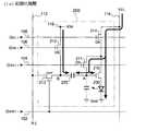
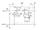
ある。そこで、画素回路200の構成を、i行j列に位置するもので代表して説明する。
図2に示されるように、画素回路200は、nチャネル型の駆動トランジスタ210と
、第1〜第4のスイッチング素子として機能するnチャネル型のトランジスタ211、2
12、213、214と、容量素子として機能する容量220と、電気光学素子たるOL
ED素子230とを有する。
このうち、トランジスタ214の一端(ドレイン)は、電源線114に接続される一方
、トランジスタ214の他端(ソース)は、駆動トランジスタ210のドレイン、および
、トランジスタ211の一端(ドレイン)に、それぞれ接続されている。ここで、トラン
ジスタ214のゲートは、i行目の制御線108に接続されている。このため、トランジ
スタ214は、制御信号GEL-iがHレベルであればオンし、Lレベルであればオフするこ
とになる。In the present embodiment, the
As shown in FIG. 2, the
12, 213, 214, a
And an
Among these, one end (drain) of the
駆動トランジスタ210のソースは、OLED素子230の陽極に接続される一方、当
該OLED素子230の陰極は、電源の低位側電圧Gndに接地されている。このため、
OLED素子230は、電源の高位側電圧VELおよび低位側電圧Gndの間の経路に、
駆動トランジスタ210およびトランジスタ214とともに電気的に介挿された構成とな
っている。
駆動トランジスタ210のゲートは、容量220の一端およびトランジスタ211のソ
ースにそれぞれ接続されている。なお、説明の便宜上、容量220の一端(駆動トランジ
スタ210のゲート)をノードAとする。このノードAには、図2において破線で示され
るように、容量が寄生する。この容量はノードAとOLED素子230の陰極の間に寄生
する容量であり、駆動トランジスタのゲート容量、OLED素子230の容量、ノードA
と陰極の間にある配線の寄生容量などに起因する容量を含んでいる。The source of the driving
The
The driving
The gate of the driving
And capacitance due to the parasitic capacitance of the wiring between the cathode and the cathode.
トランジスタ211は、駆動トランジスタ210のドレインおよびゲート間に電気的に
介挿されるとともに、トランジスタ211のゲートは、i行目の制御線104に接続され
ている。このため、トランジスタ211は、制御信号GSET-iがHレベルとなったときに
オンして、駆動トランジスタ210をダイオードとして機能させる。
一方、トランジスタ212の一端(ドレイン)は、給電線116に接続される一方、そ
の他端(ソース)は、トランジスタ213の一端(ドレイン)および容量220の他端に
それぞれ接続されている。このトランジスタ212のゲートは、i行目の制御線106に
接続されている。このため、トランジスタ212は、制御信号GINI-iがHレベルとなっ
たときにオンすることになる。
さらに、トランジスタ213の他端(ソース)は、j列目のデータ線112に接続され
、そのゲートは、i行目の走査線102に接続されている。このため、トランジスタ21
3は、走査信号GWRT-iがHレベルとなったときにオンして、j列目のデータ線112に
供給されるデータ信号X−j(の電圧)を容量220の他端に印加することになる。
ここで、説明の便宜上、容量の他端(トランジスタ212のソース、トランジスタ21
3のドレイン)をノードBとする。The
On the other hand, one end (drain) of the
Further, the other end (source) of the
3 is turned on when the scanning signal GWRT-i becomes the H level, and the data signal Xj (voltage) supplied to the
Here, for convenience of explanation, the other end of the capacitor (the source of the
3) is referred to as node B.
なお、マトリクス型に配列する画素回路200は、ガラス等の透明基板に、走査線10
2やデータ線112とともに形成されている。このため、駆動トランジスタ210や、ト
ランジスタ211、212、213、214は、ポリシリコンプロセスによるTFT(薄
膜トランジスタ)によって構成される。また、OLED素子230は、基板上において、
ITO(酸化錫インジウム)などの透明電極膜を陽極(個別電極)とし、アルミニウムや
リチウムなどの単体金属膜またはこれらの積層膜を陰極(共通電極)として、発光層を挟
持した構成となっている。Note that the
2 and the
A transparent electrode film such as ITO (indium tin oxide) is used as an anode (individual electrode), and a single metal film such as aluminum or lithium or a laminated film thereof is used as a cathode (common electrode) to sandwich a light emitting layer. .
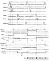
次に、電気光学装置10の動作について説明する。図3は、電気光学装置10の動作を
説明するためのタイミングチャートである。
まず、Yドライバ14は、図3に示されるように、1垂直走査期間(1F)の開始時か
ら、1行目、2行目、3行目、…、360行目の走査線102を、順番に1本ずつ1水平
走査期間(1H)毎に選択して、選択した走査線102の走査信号のみをHレベルとし、
他の走査線への走査信号をLレベルとする。
ここで、i行目の走査線102が選択されて、走査信号GWRT-iがHレベルとなる1水
平走査期間(1H)に着目して、当該水平走査期間およびその前後の動作について、図3
とともに、図4〜図8を参照して説明する。Next, the operation of the electro-
First, as shown in FIG. 3, the
The scanning signal to other scanning lines is set to L level.
Here, focusing on one horizontal scanning period (1H) in which the
A description will be given with reference to FIGS.
図3に示されるように、走査信号GWRT−iがHレベルに変化するタイミングよりも
期間Tiだけ先行したタイミングt1から、i行j列における画素回路200の書込動作
の事前準備が開始する。一方、走査信号GWRT−iがHレベルから再びLレベルに変化
すると、書き込んだ電圧に基づく発光が開始する。
このため、i行j列の画素回路200の動作については、大別すると、タイミングt1
から走査信号GWRT−iがHレベルに変化するまでの第1の期間(1)、走査信号GW
RT−iがHレベルとなる第2の期間、および、走査信号GWRT−iがLレベルに変化
した後の第3の期間、の3つにわけることができる。
これらの第1〜第3の期間については、その動作内容に着目して、それぞれ初期化期間
(1)、書込期間(2)および発光期間(3)と称することにする。このうち、初期化期
間(1)については、本実施形態では、さらに3つの期間(1a)、(1b)および(1
c)とに分けることができる。
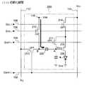
以下、これらの期間の動作について順を追って説明することにする。As shown in FIG. 3, the preparation for the writing operation of the
For this reason, the operation of the
Scan signal GW during the first period (1) from when the scan signal GWRT-i changes to the H level.
The period can be divided into a second period in which RT-i is at the H level and a third period after the scanning signal GWRT-i has changed to the L level.
These first to third periods are referred to as an initialization period (1), a writing period (2), and a light emission period (3), respectively, paying attention to the operation contents. Of these, regarding the initialization period (1), in the present embodiment, three more periods (1a), (1b) and (1)
c).
Hereinafter, the operation during these periods will be described in order.
まず、タイミングt1の前において、走査信号GWRT-i、制御信号GSET-i、GINI−
iおよびGEL-iいずれもLレベルである。そして、タイミングt1に至ると、初期化期間
(1)のうち、最初の期間(1a)となり、Yドライバ14は、制御信号GSET−i、
GINI−iおよびGEL−iをいずれもHレベルとする。このため、画素回路200で
は、図4に示されるように、Hレベルの制御信号GSET-iによりトランジスタ211がオ
ンするので、駆動トランジスタ210がダイオードとして機能する。また、Hレベルの制
御信号GEL-iによりトランジスタ214もオンする。
したがって、期間(1a)において、画素回路200では、電流が電源線114→トラ
ンジスタ214→駆動トランジスタ210→OLED素子230→接地Gndという経路
にて流れるので、ノードAは、この電流に応じた電圧、詳細には、当該電流を流す駆動ト
ランジスタ210のゲート電圧となる。
一方、制御信号GINI−iは、初期化期間(1)の全域にわたってHレベルとなって
、トランジスタ212をオンさせる。このため、ノードBは、初期化期間(1)にわたっ
て初期電圧VINIに固定されるので、容量220からみてノードBの反対側に位置するノ
ードAでは、その電圧状態が保持されることになる。したがって、期間(1a)において
ノードAは、OLED素子230に流れた電流に応じた電圧に保持されることになる。First, before the timing t1, the scanning signal GWRT-i , the control signals GSET-i , GINI-
Both i and GEL-i are at the L level. When the timing t1 is reached, the first period (1a) of the initialization period (1) is reached, and the
Both GINI-i and GEL-i are set to the H level. For this reason, in the
Therefore, in the period (1a), in the
On the other hand, the control signal GINI-i is at the H level over the entire initialization period (1) to turn on the
なお、この期間(1a)では、OLED素子230に電流が流れるので、当該OLED
素子230が発光する。ただし、この期間(1a)は、表示の単位期間である1垂直走査
期間(1F)と比較して、無視できる程度に短く設定されるので、期間(1a)での発光
は、後述する発光期間(3)における発光、すなわち、OLED素子230に目的とする
電流が流れることによる発光に影響を与えることはない。In this period (1a), since a current flows through the
The
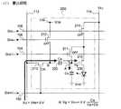
次に、初期化期間(1)の期間(1b)開始タイミングに至ると、Yドライバ14は、
制御信号GEL−iをLレベルに復帰させる一方、制御信号GSET−i、GINI−i
をともにHレベルに維持する。このため、画素回路200では、図5に示されるように、
トランジスタ214がオフするので、OLED素子230の電流経路は遮断される。ただ
し、トランジスタ211のオンが継続するので、駆動トランジスタ210が引き続きダイ
オードとして機能する。このため、ノードAは、駆動トランジスタ210のしきい値電圧
Vthnに向かって自己補償的に徐々に移行する。
そして、期間(1b)の終了タイミングでは、ノードAは、しきい値電圧Vthnにほぼ
一致することになる。Next, when the start timing of the period (1b) of the initialization period (1) is reached, the
While the control signal GEL-i is returned to the L level, the control signals GSET-i and GINI-i
Are both kept at the H level. Therefore, in the
Since the
Then, at the end timing of the period (1b), the node A substantially matches the threshold voltage Vthn .
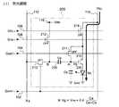
続いて、初期化期間(1)の期間(1c)の開始タイミングにおいて、Yドライバ14
は、制御信号GSET−iをLレベルに復帰させる。このため、画素回路200では、図
6に示されるように、駆動トランジスタ210のダイオード接続が解除されるので、ノー
ドAの電圧がVthnに確定することになる。Subsequently, at the start timing of the period (1c) of the initialization period (1), the
Returns the control signal GSET-i to L level. For this reason, in the
次に、書込期間(2)において、Yドライバ14は、制御信号GINI−iをLレベル
に復帰させる一方、走査信号GWRT−iをHレベルとする。このため、図7に示される
ように、トランジスタ212がオフし、トランジスタ213がオンする。
また、書込期間(2)において、Xドライバ16は、i行j列の画素の階調に応じた電
圧のデータ信号X−jをj列目のデータ線112に供給する。上述したように、画素の最
低階調を指定するデータ信号X−jの電圧がVINIであり、画素が明るく指定するにつれ
て、データ信号X−jの電圧が高くなるので、データ信号X−jの電圧は(VINI+ΔV
)として表すことができる。
なお、ΔVは、初期電圧VINIからの電圧変化(上昇)分であって、画素を最低階調の
黒色に指定する場合にはゼロであり、明るい階調を指定するにつれて次第に高くなる。し
たがって、ノードBは、初期化期間(1)から書込期間(2)にかけて、ΔVだけ変動す
る。Next, in the writing period (2), the
In the writing period (2), the
).
Note that ΔV is a voltage change (rise) from the initial voltage VINI , and is zero when the pixel is designated as the lowest gradation black, and gradually increases as the bright gradation is designated. Therefore, the node B varies by ΔV from the initialization period (1) to the writing period (2).
一方、書込期間(2)において、画素回路200では、トランジスタ211がオフであ
るので、ノードAは、駆動トランジスタ210のゲート容量のみによって保持されること
になる。このため、ノードAは、ノードBにおける電圧変化分ΔVを容量220と駆動ト
ランジスタ210のゲート容量との容量比で配分した分だけ、初期化期間(1)の電圧V
thnから上昇することになる。
詳細には、容量220のサイズをCaとし、駆動トランジスタ210のゲート容量をC
bとしたときに、ノードAは、電圧Vthnから、{ΔV・Ca /(Ca+Cb)}だ
け上昇するので、結果的に、ノードAの電圧Vgは、次式のように表すことができる。
Vg=Vthn+ΔV・Ca /(Ca+Cb)……(a)On the other hand, in the writing period (2), since the
It will rise from thn.
Specifically, the size of the
When b is set, the node A rises from the voltage Vthn by {ΔV · Ca / (Ca + Cb)}. As a result, the voltage Vg of the node A can be expressed as the following equation.
Vg = Vthn + ΔV · Ca / (Ca + Cb) (a)
そして、発光期間(3)に至ると、Yドライバ14は、走査信号GWRT−iをLレベ
ルとする一方、制御信号GEL-iをHレベルとする。
このため、画素回路200では、図8に示されるように、トランジスタ213がオフす
るが、容量220における電圧保持状態は変化しないので、ノードAは、電圧Vgに維持
される。一方、トランジスタ214がオンするので、OLED素子230には、電圧Vg
に応じた電流IELが、上記電流経路にて流れることになる。これにより、OLED素子2
30は、当該電流IELに応じた明るさで発光し続けることになる。In the light emission period (3), the
For this reason, in the
The current IEL corresponding to the current flows in the current path. Thereby, the
No. 30 continues to emit light with brightness according to the current IEL .
発光期間(3)において、OLED素子230に流れる電流IELは、駆動トランジスタ
210のソース・ドレイン間の導通状態によって定まり、当該導通状態は、ノードAの電
圧で設定される。ここで、駆動トランジスタ210のソースからみたゲートの電圧は、ノ
ードAの電圧Vgそのものであるので、電流IELは、次のように示される。
IEL=(β/2)(Vg−Vthn)2 ……(b)
なお、この式においてβは、駆動トランジスタ210の利得係数である。In the light emission period (3), the current IEL flowing through the
IEL = (β / 2) (Vg−Vthn )2 (b)
In this equation, β is a gain coefficient of the driving
ここで、式(b)に式(a)を代入して整理すると、
IEL=(β/2){ΔV・Ca /(Ca+Cb)}2 ……(c)
となる。この式(c)に示されるように、OLED素子230に流れる電流IELは、駆
動トランジスタ210のしきい値Vthnに依存することなく、初期電圧VINIからの変化分
ΔVのみによって定まることになる(容量Ca、Cbおよび利得係数βは、固定値である
)。Here, by substituting equation (a) into equation (b),
IEL = (β / 2) {ΔV · Ca / (Ca + Cb)}2 (c)
It becomes. As shown in the equation (c), the current IEL flowing through the
発光期間(3)が予め指定された期間だけ継続すると、Yドライバ14は、制御信号G
EL−iをLレベルにする。これにより、トランジスタ214がオフするので、電流経路
が遮断される結果、OLED素子230は消灯することになる。
ここで、Yドライバ14は、1行目から360行目までに対応する制御信号GEL-1〜G
EL-360のHレベル期間が同一となるように制御する。換言すれば、すべてのOLED素子
230に対して、1垂直走査期間において発光期間(3)の占める割合が一定になるよう
に制御する。このため、発光期間(3)が長くすると、画面全体が明るくなる一方、短く
すると、画面全体が暗くすることができる。
なお、発光期間(3)の最長は、1垂直走査期間(1F)のうち、初期化期間(1)お
よび書込期間(2)を除いた期間の全域である。このため、i行目でいえば、制御信号G
EL−iは、走査信号GWRT−iがHレベルからLレベルに変化するタイミングから、
1垂直走査期間(1F)経過して、再びi行目の走査線102が選択されるタイミングよ
り期間Tiだけ先行したタイミングt1までの期間でHレベルをとることができる。When the light emission period (3) continues for a predetermined period, the
Set EL-i to L level. As a result, the
Here, the
Control theEL-360 so that the H level period is the same. In other words, control is performed so that the proportion of the light emission period (3) is constant in one vertical scanning period for all the
The longest light emission period (3) is the entire period excluding the initialization period (1) and the writing period (2) in one vertical scanning period (1F). Therefore, in the i-th row, the control signal G
EL-i starts from the timing when the scanning signal GWRT-i changes from the H level to the L level.
After one vertical scanning period (1F) has passed, the H level can be taken in a period up to timing t1 preceding the timing at which the i-
ここでは、i行j列の画素回路200の動作について説明したが、i行の他の画素につ
いてもすべて初期化期間(1)、書込期間(2)および発光期間(3)の動作が同時並列
的に実行される。
また、i行目について着目して説明したが、1行目から360行目までについては、1
水平走査期間(1H)毎に順番に走査線102が選択されて、当該選択期間において書込
期間(2)の動作が実行される。そして、書込期間(2)の前には初期化期間(1)が、
書込期間(2)の後には発光期間(3)が、それぞれ実行される。例えば、i行目に続く
(i+1)行目については、図3に示されるように、走査信号GWRT-(i+1)がHレベルに
なるタイミングより期間Tiだけ先行したタイミングt2から、初期化期間(1)となり
、この後、走査信号GWRT-(i+1)がHレベルになる期間で書込期間(2)となる。(i+
1)行目の書込期間において、j列目のデータ線112には、(i+1)行j列の画素の
階調に応じた電圧のデータ信号X−jが供給されて、その電圧変化分がノードAに書き込
まれ、この後、発光期間(3)となる。
したがって、初期化期間(1)が隣接する2行以上にわたって並行して実行される場合
もあり得る。同様に、発光期間(3)も隣接する2行以上にわたって並行して実行される
。Here, the operation of the
In addition, the i-th row has been described with focus on the first row to the 360-th row.
The scanning lines 102 are sequentially selected every horizontal scanning period (1H), and the operation of the writing period (2) is executed in the selection period. Before the writing period (2), the initialization period (1)
After the writing period (2), the light emission period (3) is executed. For example, for the (i + 1) -th row following the i-th row, as shown in FIG. 3, from the timing t2 preceding the timing when the scanning signal GWRT- (i + 1) becomes the H level by the period Ti, Period (1), and then the writing period (2) is the period in which the scanning signal GWRT- (i + 1) is at the H level. (I +
1) During the writing period of the row, the data signal X-j having a voltage corresponding to the gray level of the pixel in the (i + 1) row and j column is supplied to the
Therefore, the initialization period (1) may be executed in parallel over two or more adjacent rows. Similarly, the light emission period (3) is also executed in parallel over two or more adjacent rows.
この第1実施形態によれば、初期化期間(1)のうち期間(1a)において、駆動トラ
ンジスタ210をダイオード接続し、OLED素子230に電流を強制的に流すことによ
って、ノードAを、当該電流に応じた電圧とさせる一方、ノードBを初期電圧VINIに固
定させる。このため、ノードAは、なんらかの電圧に直ちに達して保持されることになる
。この後、ダイオード接続を維持した状態で、トランジスタ214をオフさせることによ
り、期間(1b)の終了タイミングまでに、ノードAの電圧をVthnにシフトさせる。そ
して、期間(1c)において、ノードAの電圧をVthnに確定させる。この初期化期間(
1)は、行が選択される書込期間(2)とは無関係な期間であって、時間的に手前の期間
で実行されるので、1垂直走査期間(1F)において、十分に長い期間を確保することが
できる。
次に、書込期間(2)では、データ信号X−jをノードBに印加して容量220の他端
を電圧変化させ、この電圧変化による電荷の再分配によって、駆動トランジスタ210の
ゲートに、OLED素子230に流すべき電流に応じた電圧を書き込んでいる。このため
、初期化期間(1)の確保とあいまって、駆動トランジスタ210のゲートに、OLED
素子230に流すべき電流に応じた電圧を直接書き込む方式と比較して、電圧の書き込み
に要する時間を短縮化することが可能となる。
さらに、発光期間(3)において、OLED素子230に流れる電流は、駆動トランジ
スタ210のしきい値電圧Vthnに依存しない。このため、画素回路200毎に、駆動ト
ランジスタ210のしきい値電圧Vthnがバラついても、OLED素子230に流す電流
を均一に揃えることができる。
したがって、第1実施形態に係る電気光学装置によれば、高解像度化に伴って画素数が
増加しても、データ信号の書き込み時間が短くて済むとともに、OLED素子230に流
れる電流の均一性を確保することが可能となる。According to the first embodiment, in the period (1a) of the initialization period (1), the
1) is a period irrelevant to the writing period (2) in which a row is selected, and is executed in a period before the time. Therefore, a sufficiently long period is set in one vertical scanning period (1F). Can be secured.
Next, in the writing period (2), the data signal X-j is applied to the node B to change the voltage of the other end of the
Compared with a method in which a voltage corresponding to a current to be passed through the
Furthermore, in the light emission period (3), the current flowing through the
Therefore, according to the electro-optical device according to the first embodiment, even when the number of pixels increases as the resolution increases, the writing time of the data signal can be shortened, and the uniformity of the current flowing through the
なお、第1実施形態に係る画素回路200において、トランジスタ211は、オンする
ことにより駆動トランジスタ210をダイオード接続する機能を有するのに対し、トラン
ジスタ214は、オフすることによって駆動トランジスタ210およびOLED素子23
0の電流経路を遮断する機能を有するものであり、両者の機能は全く異なる。このため、
第1実施形態では、図2に示されるように、トランジスタ211については制御線104
によって、トランジスタ214については制御線108によって、それぞれ独立にオンオ
フ制御する構成とした。
しかしながら、図9に示されるように、例えばトランジスタ214の導電型をpチャネ
ル型に変更することによって、両トランジスタ211、214のチャネル型を互いに異な
らせるとともに、共通の制御線108によってオンオフ制御する構成としても良い。この
ような構成を採用すると、図2の構成と比較して、制御線104が不要となるので、制御
線が1行当たり1本削減される結果、歩留まり向上や、ボトムエミッション型の場合に開
口率を高めた明るい表示が可能となる。
また、トランジスタ211、212をともに同一のチャネル型にすると、トランジスタ
211、212のしきい値電圧が同等となるため、異なるチャネル型で構成した場合と比
して同一の制御信号GINI−iにより動作を確実に制御することができる。例えば、同
一の制御信号GINI−iに対して、一方のトランジスタがオンして、他方のトランジス
タがオフするなどの誤動作を防止することができる。また、同一のチャネル型とすること
により、トランジスタに不純物を注入する際のマージンを設ける必要がなく、トランジス
タ211とトランジスタ212とをより近接して配置することが可能である。したがって
、画素領域におけるトランジスタ占有領域を最小限とできると共に、トランジスタ211
とトランジスタ212とのトランジスタ特性をばらつきなく製造することが可能である。
さらに、駆動トランジスタ210がトランジスタ211とトランジスタ212と同一のチ
ャネル型であれば、同様の効果が得られる。また、同一のチャネル型のみにて構成するこ
とにより、画素回路に供給する信号に対する電源の電圧範囲を最低限とすることができる
ため、信頼性の高い電子回路を実現することができる。In the
It has a function of cutting off a zero current path, and the functions of both are completely different. For this reason,
In the first embodiment, as shown in FIG.
Thus, the
However, as shown in FIG. 9, for example, by changing the conductivity type of the
Further, if the
And the
Further, if the driving
<第2実施形態>
次に、本発明の第2実施形態に係る電気光学装置について説明する。この第2実施形態
に係る電気光学装置は、第1実施形態における画素回路を図10に示される画素回路20
0に置換したものである。
図2に示される画素回路200は、トランジスタ211、212のオンオフを、それぞ
れ別々の制御信号GSET-i、GINI-iによって独立に制御する構成であったが、図10に示
される画素回路は、制御線106に供給される制御信号GINI-iによって共通に制御する
構成としたものである。Second Embodiment
Next, an electro-optical device according to a second embodiment of the invention will be described. In the electro-optical device according to the second embodiment, the pixel circuit in the first embodiment is the pixel circuit 20 shown in FIG.
It has been replaced with 0.
The
図11は、第2実施形態に係る電気光学装置の動作を説明するためのタイミングチャー
トである。
この図に示されるように、第2実施形態では、制御信号GINI-iにしたがってトランジ
スタ211、212のオンオフが共通に制御されるので、初期化期間(1)には、期間(
1c)が含まれない。ただし、図10に示される画素回路200では、期間(1b)の終
了時に、トランジスタ211、212が同時にオフするので、ノードAの電圧は、初期化
期間(1b)の終了と同時に確定することになる。
なお、他の動作については、第1実施形態と同様であるので、その説明を省略する。
この第2実施形態に係る電気光学装置によれば、図9に示される画素回路と同様に、制
御線104が不要となり、制御線が1行当たり1本削減されるので、歩留まりや開口率を
向上させることができる。FIG. 11 is a timing chart for explaining the operation of the electro-optical device according to the second embodiment.
As shown in this figure, in the second embodiment, since the
1c) is not included. However, in the
Since other operations are the same as those in the first embodiment, description thereof is omitted.
According to the electro-optical device according to the second embodiment, similarly to the pixel circuit shown in FIG. 9, the
<第3実施形態>
次に、本発明の第3実施形態に係る電気光学装置について説明する。この第3実施形態
に係る電気光学装置は、第1実施形態における画素回路を図12に示される画素回路20
0に置換したものである。
図12に示される画素回路200は、図10に示した画素回路からトランジスタ214
を取り除いた構成としたものである。したがって、図12に示される画素回路200にお
いて、制御線108は不要となる。<Third Embodiment>
Next, an electro-optical device according to a third embodiment of the invention will be described. In the electro-optical device according to the third embodiment, the pixel circuit in the first embodiment is the pixel circuit 20 shown in FIG.
It has been replaced with 0.
The
It is set as the structure which removed. Therefore, the
図13は、第2実施形態に係る電気光学装置の動作を説明するためのタイミングチャー
トである。
この図に示されるように、第3実施形態では、i行目でいえば、走査信号GWRT−i
がHレベルとなる書込期間(2)よりも手前において、期間Tiだけ制御信号GINI-iが
Hレベルとなる初期化期間(1)が設けられている。
この初期化期間(1)では、トランジスタ211、212が同時にオンするので、電流
が(ダイオード接続された)駆動トランジスタ210とOLED素子230とに流れるこ
とになる。そして、初期化期間(1)の終了タイミングにおいて、制御信号GINI-iがL
レベルとなり、トランジスタ211、212が同時にオフするので、第1および第2実施
形態のように、駆動トランジスタ210のダイオード接続を継続することによる自己補償
的なノードAの電圧シフトが発生しない。FIG. 13 is a timing chart for explaining the operation of the electro-optical device according to the second embodiment.
As shown in this figure, in the third embodiment, in the i-th row, the scanning signal GWRT-i
An initialization period (1) in which the control signal GINI-i is at the H level is provided for the period Ti just before the writing period (2) at which the signal is at the H level.
In this initialization period (1), the
Since the
このため、初期化期間(1)の終了時においてノードAには、OLED素子230に流
れた電流に応じた電圧であって、駆動トランジスタ210のしきい値電圧Vthnを反映し
た電圧となり、第1および第2実施形態と比較して高くなる。そこで、第3実施形態では
、ノードAの電圧が高くなることに対応して、給電線116を介して供給される初期電圧
VINIも高く設定される。
詳細には、初期電圧VINIは、初期化期間(1)から書込期間(2)にかけてノードB
が電圧変化する際の基準電圧であり、この電圧変化に応じた電圧が書込期間(2)におい
てノードAに書き込まれる点は、第1、第2実施形態と同様である。ただし、第3実施形
態では、初期化期間(1)におけるノードAの電圧ポイントが高いので、第1、第2実施
形態と同様に初期化電圧VINIを低く設定しまうと、書込期間(2)においてノードAは
、高い電圧ポイントから上昇するだけとなり、ノードBに低い電圧を書き込んで、低階調
(暗階調)に相当する電流をOLED素子230に流すことができなくなってしまう。そ
こで、第3実施形態では、初期電圧VINIを第1、第2実施形態よりも高く設定し、初期
化期間(1)から書込期間(2)にかけてノードBが電圧上昇するのみならず、下降する
場合もありえる構成としているのである。
そして、この構成において、低階調(暗階調)に相当する電流をOLED素子230に
流す場合には、初期化期間(1)から書込期間(2)にかけてノードBが電圧下降(放電
)し、その下降分に応じた電圧がノードAに書き込まれるので、ノードBの電圧を低くし
て、低階調(暗階調)に相当する電流をOLED素子230に流すことが可能となるので
ある。
なお、第3実施形態における初期電圧VINIは、画素の最低階調(黒色)と最高階調(
白色)との間における中間階調(灰色)を指定するデータ信号の電圧に相当することにな
る。For this reason, at the end of the initialization period (1), the voltage at the node A is a voltage corresponding to the current flowing through the
Specifically, the initial voltage VINI is applied to the node B from the initialization period (1) to the writing period (2).
Is the reference voltage when the voltage changes, and the voltage corresponding to this voltage change is written to the node A in the writing period (2), as in the first and second embodiments. However, in the third embodiment, since the voltage point of the node A in the initialization period (1) is high, if the initialization voltage VINI is set low as in the first and second embodiments, the writing period (2 ), The node A only rises from a high voltage point, and a low voltage is written to the node B, so that a current corresponding to a low gradation (dark gradation) cannot flow through the
In this configuration, when a current corresponding to a low gradation (dark gradation) is supplied to the
Note that the initial voltage VINI in the third embodiment is the lowest gradation (black) and the highest gradation (black) of the pixel.
This corresponds to the voltage of the data signal designating the intermediate gray level (gray) with the white color.
この第3実施形態に係る電気光学装置によれば、図9や図10に示される画素回路と比
較して、制御線104も不要となるので、制御線が1行当たり1本(図2の画素回路と比
較すると2本)削減されるとともに、画素回路1個当たりのトランジスタ数も1個削減さ
れるので、歩留まりや開口率を、より高めることが可能となる。
ただし、第3実施形態では、トランジスタ214が存在しないので、発光期間(3)を
調整することによる画面全体の輝度調整ができない。また、書込期間(2)においても、
ノードAの電圧に応じた電流がOLED素子230に流れる。According to the electro-optical device according to the third embodiment, the
However, in the third embodiment, since the
A current corresponding to the voltage at the node A flows through the
<第4実施形態>
次に、本発明の第4実施形態に係る電気光学装置について説明する。この第4実施形態
に係る電気光学装置は、第1実施形態における画素回路を図14に示される画素回路20
0に置換したものである。
図14に示される画素回路200は、図12に示した画素回路において、電源線114
を1行毎にX方向に延設するとともに、その電圧を、時間的に変化させた構成としたもの
である。すなわち、第4実施形態における電源線114は、走査線102、制御線106
とともに1組となって、1行分の画素回路200に兼用されている。
このような電源線114は、例えばYドライバ14によって駆動される。また、第4実
施形態において、給電線116に印加される初期電圧VINIは、第1、第2実施形態と同
様に、画素の最低階調を指定するデータ信号と一致する電圧である。<Fourth embodiment>
Next, an electro-optical device according to a fourth embodiment of the invention will be described. In the electro-optical device according to the fourth embodiment, the pixel circuit in the first embodiment is the pixel circuit 20 shown in FIG.
It has been replaced with 0.
A
Are extended in the X direction for each row, and the voltage is changed with time. That is, the
A set of them is also used as a
Such a
図15は、第4実施形態に係る電気光学装置の動作を説明するためのタイミングチャー
トである。
この図に示されるように、第4実施形態では、第3実施形態と同様に、i行目でいえば
、走査信号GWRT−iがHレベルとなる書込期間(2)よりも手前の初期化期間(1)
において、制御信号GINI-iが期間TiだけHレベルとなる。
ただし、第4実施形態では、初期化期間において、Yドライバ14は、i行目の電源線
114の電圧VEL-iを初期電圧Viniとする。この初期電圧Viniは、駆動トランジスタ2
10のしきい値電圧VthnおよびOLED素子230のしきい値電圧との和よりも若干高
い程度の電圧である。詳細には、トランジスタ211のオンによってダイオード接続され
た駆動トランジスタ210のドレインに、この初期電圧Viniが印加された場合に、当該
駆動トランジスタ210およびOLED素子230に電流がごくわずかに流れる程度の電
圧である。FIG. 15 is a timing chart for explaining the operation of the electro-optical device according to the fourth embodiment.
As shown in this figure, in the fourth embodiment, as in the third embodiment, in the i-th row, the initial stage before the writing period (2) in which the scanning signal GWRT-i is at the H level is used. Period (1)
, The control signal GINI-i is at the H level for the period Ti.
However, in the fourth embodiment, during the initialization period, the
This is a voltage that is slightly higher than the sum of the
一方、第4実施形態においても、初期化期間(1)では、ノードBは、トランジスタ2
12のオンにより初期電圧VINIに固定されるので、ノードAには、当該電流に応じた電
圧が保持されることになる。
ここで、初期化期間(1)においてOLED素子230に流れる電流は、第3実施形態
とは異なり、ごくわずかであるので、ノードAに保持される電圧を、ほぼ駆動トランジス
タのしきい値Vthnとさせることができる。On the other hand, also in the fourth embodiment, in the initialization period (1), the node B is connected to the
Since the initial voltage VINI is fixed by turning on 12, the voltage corresponding to the current is held at the node A.
Here, unlike the third embodiment, the current flowing through the
次に、書込期間(2)に至ると、Yドライバ14は、電圧VEL-iをGndに落とすとも
に、制御信号GWRT−iをHレベルとする。これにより、トランジスタ213がオンす
るので、ノードBは、ΔVだけ電圧変化し、この変化分を容量比で配分した分だけ、ノー
ドAの電圧が上昇するので、第1実施形態等と同様にして、ノードAにOLED素子23
0に電流を流すためゲート電圧を書き込むことができる。
続いて、発光期間(3)に至ると、Yドライバ14は、電圧VEL-iを電源電圧VELにす
る一方、制御信号GWRT−iをLレベルとする。これにより、第1実施形態等と同様に
、OLED素子230には、ノードAの電圧に応じた電流が流れて、当該電流に応じた明
るさで発光し続けることになる。
そして、発光期間(3)が終了すると、Yドライバ14は、電圧VEL-iをGndに落と
す。これにより、OLED素子230は消灯して、発光期間(3)が調整されることなる
。Next, when the writing period (2) is reached, the
A gate voltage can be written to pass a current through zero.
Subsequently, when the light emission period (3) is reached, the
When the light emission period (3) ends, the
この第4実施形態に係る電気光学装置によれば、第3実施形態と同様に、図9や図10
に示される画素回路と比較して、制御線108が不要となるので、制御線が1行当たり1
本(図2の画素回路と比較すると2本)削減されるとともに、画素回路1個当たりのトラ
ンジスタ数も1個削減されるので、歩留まりや開口率を、より高めることが可能となる。
さらに、第4実施形態によれば、第3実施形態とは異なり、発光期間(3)を調整して、
表示画面全体の明るさを変化させることができる。
なお、第4実施形態では、電源線114を走査線102の1行毎にX方向に延設すると
したが、隣接する複数行毎に1本延設して、複数行の画素回路200にわたって兼用する
構成としても良い。このような構成とすると、配線数が削減することができるので、特に
、開口率の点で有利となる。According to the electro-optical device according to the fourth embodiment, as in the third embodiment, FIG. 9 and FIG.
Compared with the pixel circuit shown in FIG. 1, the
Since the number of transistors (two compared with the pixel circuit in FIG. 2) is reduced and the number of transistors per pixel circuit is also reduced by one, the yield and the aperture ratio can be further increased.
Furthermore, according to the fourth embodiment, unlike the third embodiment, the light emission period (3) is adjusted,
The brightness of the entire display screen can be changed.
In the fourth embodiment, the
<第5実施形態>
次に、本発明の第5実施形態に係る電気光学装置について説明する。この第5実施形態
に係る電気光学装置は、第1実施形態における画素回路を図16に示される画素回路20
0に置換したものである。
図16に示されるように、第5実施形態における画素回路200は、図14に示した画
素回路において、トランジスタ212の一端(ドレイン)の接続先を、給電線116から
、行毎の電源線114へと変更したものである。
なお、この第5実施形態に係る電気光学装置の動作は、初期化期間(1)において、ノ
ードBが電源線114の初期電圧Viniで固定される点以外、第4実施形態と同様である
ので、その説明については省略する。
この第5実施形態によれば、給電線116が不要となるので、第4実施形態と比較して
、歩留まりや開口率の点で有利となる。<Fifth Embodiment>
Next, an electro-optical device according to a fifth embodiment of the invention will be described. In the electro-optical device according to the fifth embodiment, the pixel circuit in the first embodiment is the same as the pixel circuit 20 shown in FIG.
It has been replaced with 0.
As illustrated in FIG. 16, the
The operation of the electro-optical device according to the fifth embodiment is the same as that of the fourth embodiment except that the node B is fixed at the initial voltage Vini of the
According to the fifth embodiment, the
本発明は、上述した第1〜第5実施形態に限られず、種々の変形が可能である。
例えば、各実施形態では、単色の画素について階調表示をする構成になっていたが、例
えば図17に示されるように、R(赤)、G(緑)、B(青)に対応させて画素回路20
0R、200G、200Bを配列させるとともに、これらの3画素により1ドットを構成
して、カラー表示を行うとしても良い。そして、カラー表示させる場合、OLED素子2
30R、230G、230Bは、それぞれ赤、緑、青にて発光するように発光層が選択さ
れる。
このようにカラー表示させる構成において、OLED素子230R、230G、230
Bの発光効率が互いに異なる場合には、電源電圧VELおよび初期電圧VINIを色毎に異な
らせる必要もある。
ただし、図17に示されるように、走査線102、制御線104、106および108
については共用することができる。
なお、図17は、第1実施形態(図2参照)を用いてカラー表示とする場合の構成例を
示す図である。図9や、第2実施形態(図10参照)、第3実施形態(図12参照)、第
4実施形態(図14参照)、第5実施形態(図16参照)を用いてカラー表示する構成と
して良いのはもちろんである。The present invention is not limited to the first to fifth embodiments described above, and various modifications are possible.
For example, in each embodiment, the gradation display is performed for a single pixel, but for example, as shown in FIG. 17, corresponding to R (red), G (green), and B (blue). Pixel circuit 20
In addition to arranging 0R, 200G, and 200B, one dot may be configured by these three pixels to perform color display. And when displaying in color,
The light emitting layers are selected so that 30R, 230G, and 230B emit light in red, green, and blue, respectively.
In the configuration for color display in this way, the
When the luminous efficiencies of B are different from each other, it is necessary to make the power supply voltage VEL and the initial voltage VINI different for each color.
However, as shown in FIG. 17, the
About can be shared.
FIG. 17 is a diagram showing a configuration example when color display is performed using the first embodiment (see FIG. 2). Color display using FIG. 9, the second embodiment (see FIG. 10), the third embodiment (see FIG. 12), the fourth embodiment (see FIG. 14), and the fifth embodiment (see FIG. 16). Of course it is good.
また、上述した各実施形態においては、図3、図11、図13、図15に示されるよう
に初期化期間(1)と書込期間(2)とを時間的に連続させているが、両者期間を時間的
に隔絶させても構わない。同様に、書込期間(2)と発光期間(2)とを両者期間を時間
的に隔絶させても良い。
さらに、図2、図9、図10、図14および図16の構成においては、発光期間(3)
だけでなく、書込期間(2)においても、制御信号GEL-iをHレベル、または、電圧VEL
-iを電圧VELとすることによって、ノードAの電圧に応じた電流をOLED素子230に
流す構成としても良い。In each of the embodiments described above, the initialization period (1) and the writing period (2) are temporally continuous as shown in FIG. 3, FIG. 11, FIG. 13, and FIG. Both periods may be separated in time. Similarly, the writing period (2) and the light emission period (2) may be separated in time.
Furthermore, in the configurations of FIGS. 2, 9, 10, 14 and 16, the light emission period (3)
Not only in the writing period (2), the control signal GEL-i is set to the H level or the voltage VEL.
It may be configured such that a current corresponding to the voltage at the node A flows through the
各実施形態では、駆動トランジスタ210をnチャネル型としたが、pチャネル型とし
ても良い。また、トランジスタ211、212、213、214のチャネル型についても
同様である。ただし、図9に示される構成とする場合には、トランジスタ211、214
のチャネル型については、上述したように一方をpチャネル型、他方をnチャネル型とす
る必要がある。また、図10、図12、図14または図16に示される構成とする場合に
は、トランジスタ211、212ついては、共通の制御線106によってオンまたはオフ
を同時制御するため、nまたはpの一方のチャネル型に統一する必要がある。
また、これら各トランジスタを、pチャネル型およびnチャネル型を相補型に組み合わ
せたトランスミッションゲートで構成して、電圧降下をほぼ無視できる程度に抑えても良
い。
くわえて、トランジスタ214のソース側にOLED素子230を接続するのではなく
、トランジスタ214のドレイン側にOLED素子230を接続しても良い。In each embodiment, the driving
As described above, one of the channel types must be a p-channel type and the other must be an n-channel type. In the case of the configuration shown in FIG. 10, FIG. 12, FIG. 14 or FIG. 16, the
Further, each of these transistors may be constituted by a transmission gate in which a p-channel type and an n-channel type are combined in a complementary manner, and the voltage drop may be suppressed to a level that can be almost ignored.
In addition, the
また、OLED素子230は、電流駆動型素子の一例であり、これに代えて、無機EL
素子や、フィールド・エミッション(FE)素子、LEDなどの他の発光素子、さらには
、電気泳動素子、エレクトロ・クロミック素子などを用いても良い。The
Other light emitting elements such as an element, a field emission (FE) element, and an LED, an electrophoretic element, an electrochromic element, and the like may be used.
次に、上述した実施形態に係る電気光学装置を電子機器に用いた例について説明する。
まず、上述した電気光学装置10を、表示部に適用した携帯電話について説明する。図
18は、この携帯電話の構成を示す斜視図である。
この図において、携帯電話1100は、複数の操作ボタン1102のほか、受話口11
04、送話口1106とともに、表示部として、上述した電気光学装置10を備えるもの
である。Next, an example in which the electro-optical device according to the above-described embodiment is used in an electronic device will be described.
First, a mobile phone in which the above-described electro-
In this figure, a
04, together with the
次に、上述した電気光学装置10を、ファインダに用いたデジタルスチルカメラについ
て説明する。
図19は、このデジタルスチルカメラの背面を示す斜視図である。銀塩カメラは、被写
体の光像によってフィルムを感光させるのに対し、デジタルスチルカメラ1200は、被
写体の光像をCCD(Charge Coupled Device)などの撮像素子により光電変換して撮像
信号を生成・記憶するものである。ここで、デジタルスチルカメラ1200におけるケー
ス1202の背面には、上述した電気光学装置10の表示面が設けられる。この電気光学
装置10は、撮像信号に基づいて表示を行うので、被写体を表示するファインダとして機
能することになる。また、ケース1202の前面側(図19においては裏面側)には、光
学レンズやCCDなどを含んだ受光ユニット1204が設けられている。Next, a digital still camera using the above-described electro-
FIG. 19 is a perspective view showing the back surface of the digital still camera. The silver salt camera sensitizes the film with the optical image of the subject, whereas the
撮影者が電気光学装置10によって表示された被写体像を確認して、シャッタボタン1
206を押下すると、その時点におけるCCDの撮像信号が、回路基板1208のメモリ
に転送・記憶される。また、このデジタルスチルカメラ1200にあって、ケース120
2の側面には、外部表示を行うためのビデオ信号出力端子1212と、データ通信用の入
出力端子1214とが設けられている。The photographer confirms the subject image displayed by the electro-
When 206 is pressed, the CCD image pickup signal at that time is transferred and stored in the memory of the
On the second side, a video
なお、電子機器としては、図18の携帯電話や、図19のデジタルスチルカメラの他に
も、テレビや、ビューファインダ型、モニタ直視型のビデオテープレコーダ、カーナビゲ
ーション装置、ページャ、電子手帳、電卓、ワードプロセッサ、ワークステーション、テ
レビ電話、POS端末、タッチパネルを備えた機器等などが挙げられる。そして、これら
の各種電子機器の表示部として、上述した電気光学装置が適用可能なのは言うまでもない
。また、直接画像や文字などを表示する電子機器の表示部に限られず、被感光体に光を照
射することにより間接的に画像もしくは文字を形成するために用いられる印刷機器の光源
として適用してもよい。In addition to the mobile phone shown in FIG. 18 and the digital still camera shown in FIG. 19, the electronic devices include a TV, a viewfinder type and a monitor direct view type video tape recorder, a car navigation device, a pager, an electronic notebook, and a calculator. , Word processors, workstations, videophones, POS terminals, devices with touch panels, and the like. And it cannot be overemphasized that the electro-optical apparatus mentioned above is applicable as a display part of these various electronic devices. In addition, it is not limited to a display unit of an electronic device that directly displays an image or a character, but is applied as a light source of a printing device that is used to indirectly form an image or a character by irradiating light to the photosensitive member. Also good.
10…電気光学装置、12…制御回路、14…Yドライバ、16…Xドライバ、102
…走査線、104、106、108…制御線、112…データ線、114、118…電源
線、116…給電線、200…画素回路、210…駆動トランジスタ、211、212、
213、214…トランジスタ(それぞれ第1、第2、第3、第4のスイッチング素子)
、220…容量(容量素子)、230…OLED素子(被駆動素子)、1100…携帯電
話機、1200…デジタルスチルカメラ
DESCRIPTION OF
... Scanning
213, 214 ... Transistors (first, second, third and fourth switching elements, respectively)
220 ... capacitance (capacitance element), 230 ... OLED element (driven element), 1100 ... mobile phone, 1200 ... digital still camera
Claims (16)
Translated fromJapanese前記駆動トランジスタのゲートとドレインとの間をオンまたはオフする第1のスイッチ
ング素子と、
一端が前記駆動トランジスタのゲートに接続された容量素子と
を備える電子回路の駆動方法であって、
前記容量素子の他端に初期電圧を印加するとともに、前記第1のスイッチング素子をオ
ンさせた状態にて、前記被駆動素子に電流を流し、この後、
前記電流を遮断するとともに、前記容量素子の他端に対する初期電圧の印加を解除し、
前記第1のスイッチング素子をオフさせる第1のステップと、
前記容量素子の他端に対し、前記被駆動素子に流すべき電流に応じた電圧を印加する第
2のステップと、
保持されたゲート電圧にしたがった電流を、前記駆動トランジスタが前記被駆動素子に
流す第3のステップと
を備えることを特徴とする電子回路の駆動方法。A drive transistor for controlling the current flowing through the driven element;
A first switching element that turns on or off between the gate and drain of the driving transistor;
A driving method of an electronic circuit comprising: a capacitor element having one end connected to a gate of the driving transistor,
While applying an initial voltage to the other end of the capacitive element and turning on the first switching element, a current is passed through the driven element, and then
Cutting off the current and canceling the application of the initial voltage to the other end of the capacitive element;
A first step of turning off the first switching element;
A second step of applying a voltage corresponding to a current to be passed through the driven element to the other end of the capacitive element;
A third step of driving an electronic circuit, comprising: a third step of causing the driving transistor to flow a current according to the held gate voltage to the driven element.
前記第1のスイッチング素子をオンさせるとともに前記被駆動素子に電流を流して、当
該電流に応じた電圧を、前記容量素子の一端および前記駆動トランジスタのゲートに保持
させる一方、
前記電流を遮断させた後に、前記第1のスイッチング素子をオフさせて、前記容量素子
の一端および前記駆動トランジスタのゲートに保持された電圧を、前記駆動トランジスタ
のしきい値電圧に応じた電圧に移行させる
請求項1に記載の電子回路の駆動方法。In the first step,
While turning on the first switching element and passing a current through the driven element, the voltage corresponding to the current is held at one end of the capacitive element and the gate of the driving transistor,
After the current is cut off, the first switching element is turned off, and the voltage held at one end of the capacitive element and the gate of the driving transistor is changed to a voltage corresponding to the threshold voltage of the driving transistor. The electronic circuit driving method according to claim 1, wherein the electronic circuit is driven.
前記第1のスイッチング素子をオンさせるとともに前記被駆動素子に電流を流して、当
該電流および前記駆動トランジスタのしきい値電圧に応じた電圧を、前記容量素子の一端
および前記駆動トランジスタのゲートに保持させる
請求項1に記載の電子回路の駆動方法。In the first step,
The first switching element is turned on and a current is passed through the driven element, and the voltage corresponding to the current and the threshold voltage of the driving transistor is held at one end of the capacitive element and the gate of the driving transistor The electronic circuit driving method according to claim 1.
前記第1のスイッチング素子をオンさせるとともに前記被駆動素子に電流を流した後、
前記電流の遮断とともに前記第1のスイッチング素子をオフさせて、前記駆動トランジス
タのしきい値電圧に応じた電圧を、前記容量素子の一端および前記駆動トランジスタのゲ
ートに保持させる
請求項1に記載の電子回路の駆動方法。In the first step,
After turning on the first switching element and passing a current through the driven element,
The first switching element is turned off together with the interruption of the current, and a voltage corresponding to a threshold voltage of the driving transistor is held at one end of the capacitive element and the gate of the driving transistor. Electronic circuit driving method.
前記駆動トランジスタのゲートとドレインとの間にて第1の期間においてオンし、前記
第1の期間後の第2の期間の開始タイミングまでにオフする第1のスイッチング素子と、
一端が前記駆動トランジスタのゲートに接続された容量素子と、
前記第1の期間においてオンして、初期電圧を前記容量素子の他端に印加する一方、前
記第2の期間、および、この第2の期間後の第3の期間においてオフする第2のスイッチ
ング素子と、
前記被駆動素子に流すべき電流に応じた電圧が印加される信号線と前記容量素子の他端
との間にて、前記第2の期間においてオンする第3のスイッチング素子と
を備えることを特徴とする電子回路。A drive transistor for controlling the current flowing through the driven element;
A first switching element that is turned on in a first period between the gate and drain of the driving transistor and turned off by a start timing of a second period after the first period;
A capacitive element having one end connected to the gate of the driving transistor;
Second switching that turns on in the first period and applies an initial voltage to the other end of the capacitive element, and turns off in the second period and a third period after the second period. Elements,
And a third switching element that is turned on in the second period between a signal line to which a voltage according to a current to be supplied to the driven element is applied and the other end of the capacitor element. An electronic circuit.
のゲート電圧にかかわらず、前記被駆動素子に流れる電流を遮断する第4のスイッチング
素子であって、
前記第1の期間の一部または全部の期間にオンするとともに、前記第3の期間にオンす
る第4のスイッチング素子を有する
請求項5に記載の電子回路。A fourth switching element that, when inserted into a path of a current flowing through the driven element and turned off, interrupts a current flowing through the driven element regardless of a gate voltage of the driving transistor;
The electronic circuit according to claim 5, further comprising a fourth switching element that is turned on during a part or all of the first period and turned on during the third period.
て、それらのゲートが共通の制御線に接続される
請求項6に記載の電子回路。The electronic circuit according to claim 6, wherein the first and fourth switching elements are transistors of different conductivity types, and their gates are connected to a common control line.
らのゲートが共通の制御線に接続される
請求項6に記載の電子回路。The electronic circuit according to claim 6, wherein the first and second switching elements are transistors of the same conductivity type, and their gates are connected to a common control line.
らのゲートが共通の制御線に接続される
請求項5に記載の電子回路。The electronic circuit according to claim 5, wherein the first and second switching elements are transistors of the same conductivity type, and their gates are connected to a common control line.
路に挿入され、
前記第1および第2の電源線の間の電圧は、
前記第1の期間では、前記初期電圧であり、
前記第3の期間では、所定の電源電圧となる
請求項9に記載の電子回路。The driven element and the driving transistor are inserted into a current path between the first and second power supply lines,
The voltage between the first and second power lines is:
In the first period, the initial voltage is,
The electronic circuit according to claim 9, wherein a predetermined power supply voltage is obtained in the third period.
ンとの間にてオンまたはオフする
請求項10に記載の電子回路。The electronic circuit according to claim 10, wherein the second switching element is turned on or off between the other end of the capacitive element and a drain of the driving transistor.
線との間においてオンまたはオフする
請求項6、7、8、9または10に記載の電子回路。The electronic circuit according to claim 6, 7, 8, 9 or 10, wherein the second switching element is turned on or off between the other end of the capacitive element and a power supply line to which the initial voltage is applied.
請求項5乃至12のいずれかに記載の電子回路。The electronic circuit according to claim 5, wherein the driven element is an electro-optical element.
請求項13に記載の電子回路。The electronic circuit according to claim 13, wherein the electro-optical element is an organic light-emitting diode element.
ータ線との交差に対応して画素回路を有する電気光学装置であって、
前記画素回路は、
前記電気光学素子に流れる電流を制御する駆動トランジスタと、
前記駆動トランジスタのゲートとドレインとの間にて第1の期間においてオンし、前記
第1の期間後の第2の期間の開始タイミングまでにオフする第1のスイッチング素子と、
一端が前記駆動トランジスタのゲートに接続された容量素子と、
前記第1の期間においてオンして、初期電圧を前記容量素子の他端に印加する一方、前
記第2の期間、および、この第2の期間後の第3の期間においてオフする第2のスイッチ
ング素子と、
前記データ線と前記容量素子の他端との間にて、前記第2の期間においてオンする第3
のスイッチング素子と
を備えることを特徴とする電気光学装置。An electro-optical device having a pixel circuit corresponding to the intersection of a scanning line and a data line to which a voltage corresponding to a current to be passed through the electro-optical element is applied when sequentially selected,
The pixel circuit includes:
A drive transistor for controlling a current flowing through the electro-optic element;
A first switching element that is turned on in a first period between the gate and drain of the driving transistor and turned off by a start timing of a second period after the first period;
A capacitive element having one end connected to the gate of the driving transistor;
Second switching that turns on in the first period and applies an initial voltage to the other end of the capacitive element, and turns off in the second period and a third period after the second period. Elements,
A third that is turned on in the second period between the data line and the other end of the capacitor;
An electro-optical device comprising: a switching element.
Priority Applications (3)
| Application Number | Priority Date | Filing Date | Title |
|---|---|---|---|
| JP2004126931AJP4036209B2 (en) | 2004-04-22 | 2004-04-22 | Electronic circuit, driving method thereof, electro-optical device, and electronic apparatus |
| US11/092,580US7649515B2 (en) | 2004-04-22 | 2005-03-29 | Electronic circuit, method of driving electronic circuit, electro-optical device, and electronic apparatus |
| US12/630,873US8698714B2 (en) | 2004-04-22 | 2009-12-04 | Electronic circuit, method of driving electronic circuit, electro-optical device, and electronic apparatus |
Applications Claiming Priority (1)
| Application Number | Priority Date | Filing Date | Title |
|---|---|---|---|
| JP2004126931AJP4036209B2 (en) | 2004-04-22 | 2004-04-22 | Electronic circuit, driving method thereof, electro-optical device, and electronic apparatus |
Related Child Applications (1)
| Application Number | Title | Priority Date | Filing Date |
|---|---|---|---|
| JP2007234398ADivisionJP4442666B2 (en) | 2007-09-10 | 2007-09-10 | Electronic circuit, driving method thereof, electro-optical device, and electronic apparatus |
Publications (2)
| Publication Number | Publication Date |
|---|---|
| JP2005309150Atrue JP2005309150A (en) | 2005-11-04 |
| JP4036209B2 JP4036209B2 (en) | 2008-01-23 |
Family
ID=35135909
Family Applications (1)
| Application Number | Title | Priority Date | Filing Date |
|---|---|---|---|
| JP2004126931AExpired - LifetimeJP4036209B2 (en) | 2004-04-22 | 2004-04-22 | Electronic circuit, driving method thereof, electro-optical device, and electronic apparatus |
Country Status (2)
| Country | Link |
|---|---|
| US (2) | US7649515B2 (en) |
| JP (1) | JP4036209B2 (en) |
Cited By (20)
| Publication number | Priority date | Publication date | Assignee | Title |
|---|---|---|---|---|
| JP2005326754A (en)* | 2004-05-17 | 2005-11-24 | Seiko Epson Corp | Electro-optical device, driving method thereof, and electronic apparatus |
| JP2007133369A (en)* | 2005-11-09 | 2007-05-31 | Samsung Sdi Co Ltd | Pixel and light emitting display device |
| JP2007304598A (en)* | 2006-05-09 | 2007-11-22 | Toppoly Optoelectronics Corp | Image display system |
| JP2008134625A (en)* | 2006-10-26 | 2008-06-12 | Semiconductor Energy Lab Co Ltd | Semiconductor device, display device and electronic apparatus |
| JP2008165172A (en)* | 2006-12-27 | 2008-07-17 | Samsung Sdi Co Ltd | Ambient light sensing circuit and flat panel display having the same |
| WO2008093792A1 (en)* | 2007-02-01 | 2008-08-07 | Kyocera Corporation | Image display device and method for driving image display device |
| JP2009058621A (en)* | 2007-08-30 | 2009-03-19 | Kyocera Corp | Image display device and driving method of image display device |
| JP2009157148A (en)* | 2007-12-27 | 2009-07-16 | Seiko Epson Corp | Driving method and driving method of light emitting device, electronic device |
| WO2010029795A1 (en)* | 2008-09-10 | 2010-03-18 | シャープ株式会社 | Display device and method for driving the same |
| US7755617B2 (en) | 2006-06-19 | 2010-07-13 | Seiko Epson Corporation | Electronic circuit, method for driving the same, electronic device, and electronic apparatus |
| JP2010175779A (en)* | 2009-01-29 | 2010-08-12 | Seiko Epson Corp | Driving method of unit circuit and driving method of electrooptical device |
| US7868854B2 (en) | 2006-09-13 | 2011-01-11 | Seiko Epson Corporation | Electro-optical device and electronic apparatus |
| WO2011004646A1 (en)* | 2009-07-10 | 2011-01-13 | シャープ株式会社 | Display device |
| US7928935B2 (en) | 2006-09-13 | 2011-04-19 | Seiko Epson Corporation | Electric circuit, driving method thereof, electro-optical device, and electronic apparatus |
| US8564531B2 (en) | 2010-05-26 | 2013-10-22 | Seiko Epson Corporation | Electronic apparatus and method of driving the same |
| US8581835B2 (en) | 2010-05-26 | 2013-11-12 | Seiko Epson Corporation | Electro-optical device, method for driving electro-optical device, control circuit and electronic apparatus |
| US8587513B2 (en) | 2010-05-26 | 2013-11-19 | Seiko Epson Corporation | Electro-optical device, method for driving electro-optical device, control circuit and electronic device |
| KR101389035B1 (en)* | 2006-10-26 | 2014-04-28 | 가부시키가이샤 한도오따이 에네루기 켄큐쇼 | Electronic device, display device, and semiconductor device and method for driving the same |
| US8710749B2 (en) | 2011-09-09 | 2014-04-29 | Semiconductor Energy Laboratory Co., Ltd. | Semiconductor device |
| CN111247579A (en)* | 2018-09-11 | 2020-06-05 | 株式会社矽因赛德 | Method for controlling mu LED pixel structure for completely eliminating interference of driving PMOS threshold voltage |
Families Citing this family (30)
| Publication number | Priority date | Publication date | Assignee | Title |
|---|---|---|---|---|
| TW550538B (en)* | 2002-05-07 | 2003-09-01 | Au Optronics Corp | Method of driving display device |
| TWI327594B (en)* | 2002-10-30 | 2010-07-21 | Suntory Holdings Ltd | Process goods of plants or treated products thereof , manufacturing method thereof , processing goods of ingesta , beer and plant |
| TWI288900B (en)* | 2004-04-30 | 2007-10-21 | Fujifilm Corp | Active matrix type display device |
| EP1784799A4 (en)* | 2004-08-23 | 2010-02-24 | Advance Display Technologies I | Led net display |
| KR100840116B1 (en)* | 2005-04-28 | 2008-06-20 | 삼성에스디아이 주식회사 | Light emitting display |
| JP5355080B2 (en)* | 2005-06-08 | 2013-11-27 | イグニス・イノベイション・インコーポレーテッド | Method and system for driving a light emitting device display |
| KR101373736B1 (en)* | 2006-12-27 | 2014-03-14 | 삼성디스플레이 주식회사 | Display device and driving method thereof |
| ITMI20070100A1 (en)* | 2007-01-24 | 2008-07-25 | St Microelectronics Srl | PILOT CIRCUIT OF AN OLED DIODE (ORGANIC DIODE AND LIGHT EMISSION), IN PARTICULAR FOR APPLICATION ON AM-OLED DISPLAY |
| JP4281019B2 (en)* | 2007-02-19 | 2009-06-17 | ソニー株式会社 | Display device |
| JP4300492B2 (en)* | 2007-03-13 | 2009-07-22 | ソニー株式会社 | Display device |
| JP5257075B2 (en) | 2007-06-15 | 2013-08-07 | パナソニック株式会社 | Image display device |
| US8599104B2 (en)* | 2007-11-13 | 2013-12-03 | Rgb Lights Inc. | Modular lighting and video apparatus |
| KR100922065B1 (en)* | 2008-06-11 | 2009-10-19 | 삼성모바일디스플레이주식회사 | Pixel and organic light emitting display device using same |
| KR101518742B1 (en)* | 2008-09-19 | 2015-05-11 | 삼성디스플레이 주식회사 | Display device and driving method thereof |
| KR101282996B1 (en) | 2008-11-15 | 2013-07-04 | 엘지디스플레이 주식회사 | Organic electro-luminescent display device and driving method thereof |
| KR101509113B1 (en)* | 2008-12-05 | 2015-04-08 | 삼성디스플레이 주식회사 | Display device and driving method thereof |
| CN102044212B (en)* | 2009-10-21 | 2013-03-20 | 京东方科技集团股份有限公司 | Voltage driving pixel circuit, driving method thereof and organic lighting emitting display (OLED) |
| US9984617B2 (en)* | 2010-01-20 | 2018-05-29 | Semiconductor Energy Laboratory Co., Ltd. | Display device including light emitting element |
| TW201218163A (en)* | 2010-10-22 | 2012-05-01 | Au Optronics Corp | Driving circuit for pixels of an active matrix organic light-emitting diode display and method for driving pixels of an active matrix organic light-emitting diode display |
| JP5982147B2 (en) | 2011-04-01 | 2016-08-31 | 株式会社半導体エネルギー研究所 | Light emitting device |
| US8922464B2 (en) | 2011-05-11 | 2014-12-30 | Semiconductor Energy Laboratory Co., Ltd. | Active matrix display device and driving method thereof |
| US8710505B2 (en) | 2011-08-05 | 2014-04-29 | Semiconductor Energy Laboratory Co., Ltd. | Semiconductor device |
| US10043794B2 (en) | 2012-03-22 | 2018-08-07 | Semiconductor Energy Laboratory Co., Ltd. | Semiconductor device and electronic device |
| KR20130133499A (en)* | 2012-05-29 | 2013-12-09 | 삼성디스플레이 주식회사 | Organic light emitting display device and driving method thereof |
| KR101411619B1 (en)* | 2012-09-27 | 2014-06-25 | 엘지디스플레이 주식회사 | Pixel circuit and method for driving thereof, and organic light emitting display device using the same |
| KR20140077552A (en)* | 2012-12-14 | 2014-06-24 | 삼성디스플레이 주식회사 | Organic Light Emitting Display Device and Driving Method Thereof |
| KR102218779B1 (en)* | 2014-07-04 | 2021-02-19 | 엘지디스플레이 주식회사 | Organic light emitting diode display device |
| US10375278B2 (en)* | 2017-05-04 | 2019-08-06 | Apple Inc. | Noise cancellation |
| CN109166522B (en)* | 2018-09-28 | 2022-10-18 | 昆山国显光电有限公司 | Pixel circuit, driving method thereof and display device |
| CN111489698A (en) | 2020-04-24 | 2020-08-04 | 京东方科技集团股份有限公司 | Display substrate and display device |
Family Cites Families (16)
| Publication number | Priority date | Publication date | Assignee | Title |
|---|---|---|---|---|
| US6229506B1 (en)* | 1997-04-23 | 2001-05-08 | Sarnoff Corporation | Active matrix light emitting diode pixel structure and concomitant method |
| JP3594126B2 (en)* | 2000-10-13 | 2004-11-24 | 日本電気株式会社 | Current drive circuit |
| US6734636B2 (en) | 2001-06-22 | 2004-05-11 | International Business Machines Corporation | OLED current drive pixel circuit |
| JP2003073165A (en) | 2001-08-30 | 2003-03-12 | Kyocera Corp | Zirconia sintered body for optical connector and method of manufacturing the same |
| US7456810B2 (en)* | 2001-10-26 | 2008-11-25 | Semiconductor Energy Laboratory Co., Ltd. | Light-emitting device and driving method thereof |
| JP3732477B2 (en) | 2001-10-26 | 2006-01-05 | 株式会社半導体エネルギー研究所 | Pixel circuit, light emitting device, and electronic device |
| US7071932B2 (en)* | 2001-11-20 | 2006-07-04 | Toppoly Optoelectronics Corporation | Data voltage current drive amoled pixel circuit |
| JP2003177709A (en) | 2001-12-13 | 2003-06-27 | Seiko Epson Corp | Pixel circuit for light emitting element |
| JP2003195809A (en) | 2001-12-28 | 2003-07-09 | Matsushita Electric Ind Co Ltd | EL display device, driving method thereof, and information display device |
| JP3915907B2 (en) | 2002-08-30 | 2007-05-16 | カシオ計算機株式会社 | Light emission drive circuit, display device, and drive control method thereof |
| JP4144462B2 (en)* | 2002-08-30 | 2008-09-03 | セイコーエプソン株式会社 | Electro-optical device and electronic apparatus |
| JP3832415B2 (en)* | 2002-10-11 | 2006-10-11 | ソニー株式会社 | Active matrix display device |
| JP2004286816A (en) | 2003-03-19 | 2004-10-14 | Toshiba Matsushita Display Technology Co Ltd | Active matrix type display device and its driving method |
| JP4484451B2 (en)* | 2003-05-16 | 2010-06-16 | 奇美電子股▲ふん▼有限公司 | Image display device |
| TW200540774A (en)* | 2004-04-12 | 2005-12-16 | Sanyo Electric Co | Organic EL pixel circuit |
| JP4974471B2 (en) | 2004-04-12 | 2012-07-11 | 三洋電機株式会社 | Organic EL pixel circuit and driving method thereof |
- 2004
- 2004-04-22JPJP2004126931Apatent/JP4036209B2/ennot_activeExpired - Lifetime
- 2005
- 2005-03-29USUS11/092,580patent/US7649515B2/enactiveActive
- 2009
- 2009-12-04USUS12/630,873patent/US8698714B2/enactiveActive
Cited By (39)
| Publication number | Priority date | Publication date | Assignee | Title |
|---|---|---|---|---|
| JP2005326754A (en)* | 2004-05-17 | 2005-11-24 | Seiko Epson Corp | Electro-optical device, driving method thereof, and electronic apparatus |
| JP2007133369A (en)* | 2005-11-09 | 2007-05-31 | Samsung Sdi Co Ltd | Pixel and light emitting display device |
| JP2007304598A (en)* | 2006-05-09 | 2007-11-22 | Toppoly Optoelectronics Corp | Image display system |
| JP2007304594A (en)* | 2006-05-09 | 2007-11-22 | Toppoly Optoelectronics Corp | Image display system and method for driving display elements |
| US7755617B2 (en) | 2006-06-19 | 2010-07-13 | Seiko Epson Corporation | Electronic circuit, method for driving the same, electronic device, and electronic apparatus |
| KR101442052B1 (en) | 2006-09-13 | 2014-09-18 | 세이코 엡슨 가부시키가이샤 | Electro-optical device and electronic apparatus |
| US7928935B2 (en) | 2006-09-13 | 2011-04-19 | Seiko Epson Corporation | Electric circuit, driving method thereof, electro-optical device, and electronic apparatus |
| US7868854B2 (en) | 2006-09-13 | 2011-01-11 | Seiko Epson Corporation | Electro-optical device and electronic apparatus |
| JP7535630B2 (en) | 2006-10-26 | 2024-08-16 | 株式会社半導体エネルギー研究所 | Display device |
| JP2020016887A (en)* | 2006-10-26 | 2020-01-30 | 株式会社半導体エネルギー研究所 | Display device |
| KR101389035B1 (en)* | 2006-10-26 | 2014-04-28 | 가부시키가이샤 한도오따이 에네루기 켄큐쇼 | Electronic device, display device, and semiconductor device and method for driving the same |
| US8803768B2 (en) | 2006-10-26 | 2014-08-12 | Semiconductor Energy Laboratory Co., Ltd. | Electronic device, display device, and semiconductor device and method for driving the same |
| US11887535B2 (en) | 2006-10-26 | 2024-01-30 | Semiconductor Energy Laboratory Co., Ltd. | Electronic device, display device, and semiconductor device and method for driving the same |
| JP2008134625A (en)* | 2006-10-26 | 2008-06-12 | Semiconductor Energy Lab Co Ltd | Semiconductor device, display device and electronic apparatus |
| JP2023134470A (en)* | 2006-10-26 | 2023-09-27 | 株式会社半導体エネルギー研究所 | Display |
| JP2017142524A (en)* | 2006-10-26 | 2017-08-17 | 株式会社半導体エネルギー研究所 | Display device |
| US10546529B2 (en) | 2006-10-26 | 2020-01-28 | Semiconductor Energy Laboratory Co., Ltd. | Electronic device, display device, and semiconductor device and method for driving the same |
| JP2021103322A (en)* | 2006-10-26 | 2021-07-15 | 株式会社半導体エネルギー研究所 | Display |
| JP2008165172A (en)* | 2006-12-27 | 2008-07-17 | Samsung Sdi Co Ltd | Ambient light sensing circuit and flat panel display having the same |
| US8325116B2 (en) | 2007-02-01 | 2012-12-04 | Lg Display Co., Ltd. | Image display apparatus, and image display apparatus driving method |
| WO2008093792A1 (en)* | 2007-02-01 | 2008-08-07 | Kyocera Corporation | Image display device and method for driving image display device |
| JP2008191247A (en)* | 2007-02-01 | 2008-08-21 | Kyocera Corp | Image display device and driving method of image display device |
| JP2009058621A (en)* | 2007-08-30 | 2009-03-19 | Kyocera Corp | Image display device and driving method of image display device |
| JP2009157148A (en)* | 2007-12-27 | 2009-07-16 | Seiko Epson Corp | Driving method and driving method of light emitting device, electronic device |
| WO2010029795A1 (en)* | 2008-09-10 | 2010-03-18 | シャープ株式会社 | Display device and method for driving the same |
| US8854343B2 (en) | 2008-09-10 | 2014-10-07 | Sharp Kabushiki Kaisha | Display device and method for driving the same |
| JP5172963B2 (en)* | 2008-09-10 | 2013-03-27 | シャープ株式会社 | Display device and driving method thereof |
| JP2013101373A (en)* | 2008-09-10 | 2013-05-23 | Sharp Corp | Display device and driving method thereof |
| JP2010175779A (en)* | 2009-01-29 | 2010-08-12 | Seiko Epson Corp | Driving method of unit circuit and driving method of electrooptical device |
| JP5214030B2 (en)* | 2009-07-10 | 2013-06-19 | シャープ株式会社 | Display device |
| US8605077B2 (en) | 2009-07-10 | 2013-12-10 | Sharp Kabushiki Kaisha | Display device |
| WO2011004646A1 (en)* | 2009-07-10 | 2011-01-13 | シャープ株式会社 | Display device |
| US8581835B2 (en) | 2010-05-26 | 2013-11-12 | Seiko Epson Corporation | Electro-optical device, method for driving electro-optical device, control circuit and electronic apparatus |
| US8564531B2 (en) | 2010-05-26 | 2013-10-22 | Seiko Epson Corporation | Electronic apparatus and method of driving the same |
| US8587513B2 (en) | 2010-05-26 | 2013-11-19 | Seiko Epson Corporation | Electro-optical device, method for driving electro-optical device, control circuit and electronic device |
| US9082670B2 (en) | 2011-09-09 | 2015-07-14 | Semiconductor Energy Laboratory Co., Ltd. | Semiconductor device |
| US8901828B2 (en) | 2011-09-09 | 2014-12-02 | Semiconductor Energy Laboratory Co., Ltd. | Semiconductor device |
| US8710749B2 (en) | 2011-09-09 | 2014-04-29 | Semiconductor Energy Laboratory Co., Ltd. | Semiconductor device |
| CN111247579A (en)* | 2018-09-11 | 2020-06-05 | 株式会社矽因赛德 | Method for controlling mu LED pixel structure for completely eliminating interference of driving PMOS threshold voltage |
Also Published As
| Publication number | Publication date |
|---|---|
| JP4036209B2 (en) | 2008-01-23 |
| US20100079357A1 (en) | 2010-04-01 |
| US8698714B2 (en) | 2014-04-15 |
| US7649515B2 (en) | 2010-01-19 |
| US20050237273A1 (en) | 2005-10-27 |
Similar Documents
| Publication | Publication Date | Title |
|---|---|---|
| JP4036209B2 (en) | Electronic circuit, driving method thereof, electro-optical device, and electronic apparatus | |
| JP4033166B2 (en) | Electronic circuit, driving method thereof, electro-optical device, and electronic apparatus | |
| US11551617B2 (en) | Display device, electronic device, and driving method of display device | |
| US8232936B2 (en) | Electronic circuit, method of driving the same, electro-optical device, and electronic apparatus | |
| JP4442666B2 (en) | Electronic circuit, driving method thereof, electro-optical device, and electronic apparatus | |
| US8947327B2 (en) | Display apparatus, driving method thereof, and electronic system | |
| JP3772889B2 (en) | Electro-optical device and driving device thereof | |
| JP4752331B2 (en) | Light emitting device, driving method and driving circuit thereof, and electronic apparatus | |
| CN101312008B (en) | Display device, display device driving method, and electronic device | |
| US8982016B2 (en) | Display device, driving method thereof, and electronic device | |
| JP2005115144A (en) | Pixel circuit driving method, driving circuit, electro-optical device, and electronic apparatus | |
| JP4797336B2 (en) | Electro-optical device and electronic apparatus | |
| KR100749110B1 (en) | Pixel circuit, method of driving the same, electro-optical device, and electronic apparatus |
Legal Events
| Date | Code | Title | Description |
|---|---|---|---|
| RD04 | Notification of resignation of power of attorney | Free format text:JAPANESE INTERMEDIATE CODE: A7424 Effective date:20070403 | |
| A977 | Report on retrieval | Free format text:JAPANESE INTERMEDIATE CODE: A971007 Effective date:20070704 | |
| A131 | Notification of reasons for refusal | Free format text:JAPANESE INTERMEDIATE CODE: A131 Effective date:20070710 | |
| A521 | Request for written amendment filed | Free format text:JAPANESE INTERMEDIATE CODE: A523 Effective date:20070910 | |
| RD02 | Notification of acceptance of power of attorney | Free format text:JAPANESE INTERMEDIATE CODE: A7422 Effective date:20070910 | |
| TRDD | Decision of grant or rejection written | ||
| A01 | Written decision to grant a patent or to grant a registration (utility model) | Free format text:JAPANESE INTERMEDIATE CODE: A01 Effective date:20071009 | |
| A61 | First payment of annual fees (during grant procedure) | Free format text:JAPANESE INTERMEDIATE CODE: A61 Effective date:20071022 | |
| R150 | Certificate of patent or registration of utility model | Ref document number:4036209 Country of ref document:JP Free format text:JAPANESE INTERMEDIATE CODE: R150 Free format text:JAPANESE INTERMEDIATE CODE: R150 | |
| FPAY | Renewal fee payment (event date is renewal date of database) | Free format text:PAYMENT UNTIL: 20101109 Year of fee payment:3 | |
| FPAY | Renewal fee payment (event date is renewal date of database) | Free format text:PAYMENT UNTIL: 20101109 Year of fee payment:3 | |
| FPAY | Renewal fee payment (event date is renewal date of database) | Free format text:PAYMENT UNTIL: 20111109 Year of fee payment:4 | |
| FPAY | Renewal fee payment (event date is renewal date of database) | Free format text:PAYMENT UNTIL: 20111109 Year of fee payment:4 | |
| FPAY | Renewal fee payment (event date is renewal date of database) | Free format text:PAYMENT UNTIL: 20121109 Year of fee payment:5 | |
| FPAY | Renewal fee payment (event date is renewal date of database) | Free format text:PAYMENT UNTIL: 20121109 Year of fee payment:5 | |
| FPAY | Renewal fee payment (event date is renewal date of database) | Free format text:PAYMENT UNTIL: 20131109 Year of fee payment:6 | |
| S531 | Written request for registration of change of domicile | Free format text:JAPANESE INTERMEDIATE CODE: R313531 | |
| R350 | Written notification of registration of transfer | Free format text:JAPANESE INTERMEDIATE CODE: R350 | |
| EXPY | Cancellation because of completion of term |