JP2005303111A - Semiconductor memory device - Google Patents
Semiconductor memory deviceDownload PDFInfo
- Publication number
- JP2005303111A JP2005303111AJP2004118709AJP2004118709AJP2005303111AJP 2005303111 AJP2005303111 AJP 2005303111AJP 2004118709 AJP2004118709 AJP 2004118709AJP 2004118709 AJP2004118709 AJP 2004118709AJP 2005303111 AJP2005303111 AJP 2005303111A
- Authority
- JP
- Japan
- Prior art keywords
- field effect
- insulated gate
- memory device
- semiconductor memory
- high dielectric
- Prior art date
- Legal status (The legal status is an assumption and is not a legal conclusion. Google has not performed a legal analysis and makes no representation as to the accuracy of the status listed.)
- Pending
Links
Images


Landscapes
- Static Random-Access Memory (AREA)
- Metal-Oxide And Bipolar Metal-Oxide Semiconductor Integrated Circuits (AREA)
- Semiconductor Memories (AREA)
Abstract
Description
Translated fromJapanese 本発明は、半導体記憶装置に関するものである。わけてもSRAM(Static
Randum Access Memory:スタティックランダムアクセスメモリ)ないしはこれに相当する半導体記憶装置に関する。本発明は、その小面積化を確保しつつ低リーク化する技術を提供するものである。The present invention relates to a semiconductor memory device. Especially SRAM (Static
The present invention relates to a semiconductor memory device or a corresponding random access memory (Randum Access Memory). The present invention provides a technique for reducing leakage while ensuring a small area.
SRAMは、半導体情報処理装置のワークメモリとして広く使われている。特にマイクロプロセッサ用ワークメモリとして、構造上論理回路のプロセスで構成できるため、同じ半導体基板上に集積化されている。近年、マイクロプロセッサは高性能・高機能となってきており、同一基板上のSRAMはこれに対応するため、高速且つ高集積が求められている。加えて、携帯機器が広がり、ここにマイクロプロセッサの大きな市場が広がっている。これは電池動作が前提であるので、低電力化、それも待機電力の低減が求められている。待機電力(電流)は始終流れ続けるので、これを大きく低減しないと、電池は直ぐにその容量を使い切ってしまうのである。 An SRAM is widely used as a work memory of a semiconductor information processing apparatus. In particular, as a work memory for a microprocessor, since it can be structured by a process of a logic circuit, it is integrated on the same semiconductor substrate. In recent years, microprocessors have become high-performance and high-function, and SRAMs on the same substrate are required to be fast and highly integrated. In addition, portable devices are spreading, and here is a large market for microprocessors. Since this is premised on battery operation, there is a demand for lower power and lower standby power. Since standby power (current) continues to flow from start to finish, the battery will soon run out of its capacity unless it is greatly reduced.
一方、SRAMは、一般的にMOSトランジスタ(Metal−Oxside−Semiconductor型(絶縁ゲート型)電界効果トランジスタ)を2つ用いたインバータを2つ用いてフリップフロップを構成し、これに情報の読み書きを行う2つのMOSトランジスタを更に使用し、合計6ヶのMOSトランジスタで構成されている。これを4ヶのMOSトランジスタで構成したものが、例えば、IEEE TRANSACTIONS ON ELECTRON DEVOCES、VOL.48、No.12、2001年12月、2851頁〜2855頁に報告されている(非特許文献1)。 On the other hand, an SRAM generally forms a flip-flop using two inverters using two MOS transistors (Metal-Oxide-Semiconductor type (insulated gate type) field effect transistors), and reads / writes information from / to this. Two MOS transistors are further used to form a total of six MOS transistors. This is composed of four MOS transistors, for example, IEEE TRANSACTIONS ON ELECTRON DEVESES, VOL. 48, no. 12, December 2001, pages 2851 to 2855 (Non-patent Document 1).
又、これら半導体技術で使われるCMOS(相補型(Complementary)MOS)では、性能を向上させるためにその絶縁膜の薄膜化が著しい。しかしながら、薄くなりすぎるとトンネル効果が電流が流れ出し、これが待機電流を増大させてしまうため、高誘電膜をこの絶縁膜に用いて性能向上を維持したままで膜を厚くする検討が始まっている。半導体での技術世代を表わす用語で言えば、65nm(ナノメートル)以降での採用が目論まれている。 In addition, in the CMOS (Complementary MOS) used in these semiconductor technologies, the insulating film is significantly thinned in order to improve the performance. However, if the film becomes too thin, the tunneling effect causes a current to flow, which increases the standby current. Therefore, studies have been started to use a high dielectric film as the insulating film to increase the film thickness while maintaining the performance improvement. Speaking of terms representing the technology generation in semiconductors, adoption at 65 nm (nanometers) and beyond is being planned.
4ヶのMOSトランジスタで構成したSRAMの回路例を図16に示す。この形態のSRAMは、従来使われていた6ヶのMOSトランジスタで構成したSRAMに比べて素子数が少ないため小面積となり、その分、高集積化が可能である。図16に例示されるように、MOSトランジスタMN1とMN2とが、互いのドレイン端子を相手のゲート端子に接続している。例えば、MOSトランジスタMN1のドレイン端子N1は、MN2のゲート端子となっている。他方のMOSトランジスタに対するドレイン端子はN2と示される。この端子N1とN2の電位差によって情報を保持する。ソース端子は共通となりVSMとなっている。情報保持時において、MOSトランジスタMP1とMP2は、負荷素子となっている。即ち、これらのMOSトランジスタのゲート端子につながるワード線WLが接続され、情報保持時にはこれらのMP1とMP2はオフ状態となっている。このオフ状態の時のリーク電流を利用して次に説明するように情報を保持している。又、MOSトランジスタMP1とMP2は、情報の読み書きを行う機能を兼ねている。この時は、ワード線電圧を変化させてMOSトランジスタMP1とMP2をオンさせ、ビット線BT、BBと情報を保持している内部ノードN1、N2とを接続する。この図においては、MOSトランジスタMN1とMN2とはnチャネル型MOSトランジスタであり、MOSトランジスタMP1とMP2はpチャネル型MOSトランジスタである。これらの導電性をひっくり返して所望のソース電圧を与えることによっても、4ヶのMOSトランジスタで構成したSRAMが実現できる。 FIG. 16 shows a circuit example of an SRAM constituted by four MOS transistors. The SRAM of this form has a small area because the number of elements is smaller than that of an SRAM composed of six MOS transistors used in the prior art, and can be highly integrated accordingly. As illustrated in FIG. 16, the MOS transistors MN1 and MN2 have their drain terminals connected to the other gate terminal. For example, the drain terminal N1 of the MOS transistor MN1 is the gate terminal of MN2. The drain terminal for the other MOS transistor is designated N2. Information is held by the potential difference between the terminals N1 and N2. The source terminal is common and is VSM. At the time of information holding, the MOS transistors MP1 and MP2 are load elements. That is, a word line WL connected to the gate terminals of these MOS transistors is connected, and these MP1 and MP2 are in an off state when information is held. Information is held as described below by using the leakage current in the off state. The MOS transistors MP1 and MP2 also have a function of reading and writing information. At this time, the word line voltage is changed to turn on the MOS transistors MP1 and MP2, and the bit lines BT and BB are connected to the internal nodes N1 and N2 holding information. In this figure, MOS transistors MN1 and MN2 are n-channel MOS transistors, and MOS transistors MP1 and MP2 are p-channel MOS transistors. An SRAM constituted by four MOS transistors can also be realized by turning over these conductivity and applying a desired source voltage.
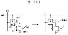
この時の難点を、図19A及び図19Bを用いて説明する。即ち、情報保持時に大きなリーク電流が流れてしまうという難点である。図19A及び図19Bでは、図18の回路における左半分を図19Aに、右半分を及び図19Bに示している。そして、そのそれぞれの図の左半分が説明のための図、右半分が実際に流れる電流の状態を示している。ここでは、端子VSMの電位を基準に、内部ノードN1に高電位、内部ノードN2に低電位が現れており、この情報を保持している状態を示している。これが、例えば“1”に相当し、図では示していないが反対の電位である内部ノードN1に低電位、内部ノードN2に高電位が“0”に相当する。情報保持状態であるのでMOSトランジスタMP1とMP2はオフ状態である。図19Aの左の図において、MP1はオフであり、これにリーク電流が流れようとする。この流れようとする仮想的な電流をIP1と置く。この時、MOSトランジスタMN1に流れようとする仮想的な電流をIN1と置く。MN1のゲートであるN1には低電位、ドレインであるN2には高電位を発生させようとしている。つまり、N1には低電位であり、VSMとの電位差が小さく、MN1をよりオフ状態にしようとする。この時、nチャネルMOSトランジスタMN1に流れようとする仮想的な電流をIN1が、pチャネルMOSトランジスタMP1に流れようとする仮想的な電流をIP1よりも大きければ、N1の電位は上昇し、平衡点として、図19Aの右の電流I1が流れることとなる。プロセス変動、温度変動を考慮すると、この仮想的な電流をIP1は仮想的な電流をIN1よりも2桁大きくなければならない。従って、平衡点での電流であるI1は殆どIN1の値で決まってしまう。 The difficulty at this time will be described with reference to FIGS. 19A and 19B. That is, there is a problem that a large leak current flows when holding information. 19A and 19B, the left half of the circuit of FIG. 18 is shown in FIG. 19A, and the right half is shown in FIG. 19B. And the left half of each figure shows the figure for description, and the right half has shown the state of the electric current which actually flows. Here, with reference to the potential of the terminal VSM, a high potential appears at the internal node N1 and a low potential appears at the internal node N2, and this information is held. This corresponds to, for example, “1”, and although not shown in the drawing, the internal node N1, which is the opposite potential, corresponds to a low potential and the internal node N2 corresponds to a high potential “0”. Since the information is held, the MOS transistors MP1 and MP2 are off. In the left diagram of FIG. 19A, MP1 is off, and a leak current tends to flow through it. This virtual current to flow is set as IP1. At this time, a virtual current that is about to flow through the MOS transistor MN1 is set as IN1. A low potential is generated at N1 which is the gate of MN1, and a high potential is generated at N2 which is the drain. That is, N1 has a low potential, and the potential difference from VSM is small, so that MN1 is more turned off. At this time, if IN1 is a virtual current that flows through n-channel MOS transistor MN1 and IP1 is a virtual current that flows through p-channel MOS transistor MP1, the potential of N1 rises and balances. As a point, the current I1 on the right in FIG. 19A flows. In consideration of process variation and temperature variation, IP1 must be larger by two orders of magnitude than IN1. Accordingly, the current I1 at the equilibrium point is almost determined by the value of IN1.
図19Bに示す図18の回路における右半分では次の課題が生じる。ワード線WLがMOSトランジスタMP1とMP2とで共通である。又、ビット線BB、BTは情報保持時では同じ電位であり、例えばこのワード線と同じ電位である。よって、MOSトランジスタMP2に流れようとする仮想的な電流をIP2は、IP1と同じで大きさとなる。これは前述の如く、IN1よりも2桁大きい電流である。一方、MOSトランジスタMN2ではそのゲートであるN1の電位はVSMを基準としてN2より高く、このMN2はオンしている。これによって、N2の電位は低く保たれる。このようにして情報は安定に保持される。しかしながら、この時、MOSトランジスタMN2はオンであるため、MP2に流れようとする仮想的な電流IP2と殆ど変わらない電流が流れてしまう。これをI2と示した。これはIP2と殆ど同じであるから、前述のようにIN1よりも2桁大きい電流である。この電流によって、情報保持時に電流が流れ、待機時の電力増加させてしまう。これは、電池動作が前提の携帯機器に応用する時に、大きな問題となる。 In the right half of the circuit of FIG. 18 shown in FIG. 19B, the following problem occurs. The word line WL is common to the MOS transistors MP1 and MP2. Further, the bit lines BB and BT are at the same potential when information is held, for example, the same potential as this word line. Therefore, the virtual current that is about to flow through the MOS transistor MP2 is the same as IP1 and has the same magnitude. As described above, this is a current that is two orders of magnitude larger than IN1. On the other hand, in the MOS transistor MN2, the potential of N1, which is the gate thereof, is higher than N2 with respect to VSM, and this MN2 is on. As a result, the potential of N2 is kept low. In this way, information is held stably. However, at this time, since the MOS transistor MN2 is on, a current that is almost the same as the virtual current IP2 that flows to MP2 flows. This was designated as I2. Since this is almost the same as IP2, it is a current two orders of magnitude larger than IN1 as described above. This current causes a current to flow when information is held, and increases power during standby. This becomes a big problem when applied to a portable device on the premise of battery operation.
本発明は、SRAM(Static Randum Access Memory:スタティックランダムアクセスメモリ)ないしはこれに相当する半導体記憶装置において、その小面積化を確保しつつ低リーク化する技術を提供する。 The present invention provides a technology for reducing leakage while securing a small area in a static random access memory (SRAM) or a semiconductor memory device corresponding to the static random access memory (SRAM).
本発明の第1の観点は、4つのMOSトランジスタで構成したSRAMにおいて、同じ導電性の2つのMOSトランジスタのゲート絶縁膜が、当該SRAMの有するMOSトランジスタのI−V特性がヒステリシス(履歴)特性を持つ高誘電体膜で構成されている半導体記憶装置である。尚、SRAMは、2つのMOSトランジスタでクロスカップルを構成し、その2つの出力端の各々に、逆導電型のMOSトランジスタを接続したメモリセルで構成される。 According to a first aspect of the present invention, in an SRAM constituted by four MOS transistors, the gate insulating film of two MOS transistors having the same conductivity is used, and the IV characteristic of the MOS transistor of the SRAM is a hysteresis (history) characteristic. This is a semiconductor memory device composed of a high dielectric film having The SRAM is configured by a memory cell in which two MOS transistors form a cross couple, and reverse conductivity type MOS transistors are connected to each of the two output terminals.
本発明の半導体記憶装置は、リーク電流が発生しても、基本的な回路動作はSRAMに準拠するので、SRAMあるいはSRAM相当の半導体記憶装置を含め、本明細書では、そのリーク電流の大きさによらず、以下、単にSRAMと称することとする。 Since the semiconductor memory device of the present invention conforms to the SRAM even if a leak current occurs, the basic circuit operation conforms to the SRAM. Therefore, in the present specification, including the semiconductor memory device equivalent to the SRAM or the SRAM, the magnitude of the leak current is described. Regardless, it will be hereinafter simply referred to as SRAM.
本発明の第2の観点は、4つのMOSトランジスタで構成したSRAMと論理回路とを備え、共にゲート絶縁膜として高誘電体膜を用いるLSIにおいて、SRAMの印可電圧を、高誘電体膜が履歴を持つまで高くする半導体記憶装置である。 According to a second aspect of the present invention, in an LSI including an SRAM composed of four MOS transistors and a logic circuit, both of which use a high dielectric film as a gate insulating film, the applied voltage of the SRAM is a history of the high dielectric film. It is a semiconductor memory device which is made high until it has.
本発明の第3の観点は、4つのMOSトランジスタで構成したSRAMと論理回路とを備え、共にゲート絶縁膜として高誘電体膜を用いるLSIにおいて、SRAMで用いる高誘電体膜の厚さが、論理回路での高誘電体膜の厚さよりも大きいものも含む半導体記憶装置である。 According to a third aspect of the present invention, in an LSI including an SRAM composed of four MOS transistors and a logic circuit, both of which use a high dielectric film as a gate insulating film, the thickness of the high dielectric film used in the SRAM is: This is a semiconductor memory device including a device having a thickness larger than the thickness of the high dielectric film in the logic circuit.
このように、本発明のゲート絶縁膜に基づく電圧−電流特性がヒステリシス特性を実現するには、当該ゲート絶縁膜の厚さを制御する方法、メモリセルへの印加電圧を制御する方法がある。更には、その両者を併用する方法などを取ることが出来る。 As described above, there are a method for controlling the thickness of the gate insulating film and a method for controlling the voltage applied to the memory cell in order to realize the hysteresis characteristic of the voltage-current characteristic based on the gate insulating film of the present invention. Furthermore, the method of using both of them can be taken.
又、具体的には、メモリセルは、第1の導電型のチャネルを有する、第1及び第2の絶縁ゲート型電界効果型トランジスタが、互いのドレイン端子が相手のゲート端子に接続され、互いのソース端子が共通に接続されて配されたクロスカップルと、当該クロスカップルの2つの出力端の各々に、第2の導電型のチャネルを有する、第3及び第4の絶縁ゲート型電界効果型トランジスタの一方の端子が各々接続された構成を有するが、この時、前記第1及び第2の絶縁ゲート型電界効果型トランジスタは、nチャネル型(或いはpチャネル型)絶縁ゲート型電界効果型トランジスタ、一方前記第3及び第4の絶縁ゲート型電界効果型トランジスタは、pチャネル型(或いはnチャネル型)絶縁ゲート型電界効果型トランジスタを用いることが出来る。尚、前記第3及び第4の絶縁ゲート型電界効果型トランジスタはいわゆる転送MOSトランジスタの役割を担っている。 Specifically, the memory cell includes first and second insulated gate field effect transistors each having a first conductivity type channel, each having a drain terminal connected to the other gate terminal, A third couple and a fourth insulated gate field effect type having a cross couple in which source terminals of the cross couple are connected in common and a channel of the second conductivity type at each of two output ends of the cross couple One terminal of the transistor is connected to each other. At this time, the first and second insulated gate field effect transistors are n-channel (or p-channel) insulated gate field effect transistors. On the other hand, the third and fourth insulated gate field effect transistors may be p-channel (or n-channel) insulated gate field effect transistors. That. The third and fourth insulated gate field effect transistors play the role of so-called transfer MOS transistors.
本発明では、前述したCMOSの絶縁膜に用いる高誘電体膜を利用することを可能とする。この高誘電体膜を通常のCMOSにて用いる場合よりも厚くしたり、或いは動作電圧範囲を広く取ることによって、履歴を持たせられることに着目する。一般に、CMOSへの適用では、この履歴が出ないように一定厚さ以下としたり、電圧を低くしたり、プロセスを追加したりするのだが、発明者等はこのようなことをSRAMの領域で行わなければ、履歴が生じ、これを用いれば上記課題が解決できるという発想に思い至った。これによって、ゲート電圧が高い状態から低い状態には移り難くなり、同時に、ゲート電圧が低い状態から高い状態へも移り難くなる。即ち、ここで情報の保持の補助が行われる。これを、前述のMN1、MN2に適用すれば、より小さな電流での情報の保持を安定に行うことができる。このために待機電流を低減させることができる。 The present invention makes it possible to use the high dielectric film used for the above-described CMOS insulating film. It is noted that the history can be provided by making this high dielectric film thicker than in the case of using a normal CMOS or by taking a wide operating voltage range. Generally, in application to CMOS, the thickness is set to a certain thickness or less so that this history does not occur, the voltage is lowered, or a process is added. However, the inventors do this in the SRAM area. If it is not done, a history will be generated, and if this is used, it came to the idea that the above problems could be solved. As a result, it becomes difficult to shift from a high gate voltage state to a low state, and at the same time, it is difficult to shift from a low gate voltage state to a high state. In other words, information holding assistance is performed here. If this is applied to the above-described MN1 and MN2, information can be stably held with a smaller current. For this reason, standby current can be reduced.
このように、4ヶのMOSトランジスタで構成した面積の小さなSRAMにおいて、CMOSで使われる高誘電膜を用いて情報保持時の電流を低減できる。これによって、小面積且つ低待機電力であるSRAMを実現することができる。 As described above, in a small-area SRAM composed of four MOS transistors, the current at the time of holding information can be reduced by using the high dielectric film used in the CMOS. As a result, an SRAM having a small area and low standby power can be realized.
本発明は、小面積を確保しつつ且つ低待機電力である半導体記憶装置を提供する。 The present invention provides a semiconductor memory device that secures a small area and has low standby power.
本発明は、プロセッサなどの論理回路と同一チップ上のSRAMに適用して有用である。本発明は、特に、携帯機器用のシステムLSIのオンチップSRAMに最適である。 The present invention is useful when applied to an SRAM on the same chip as a logic circuit such as a processor. The present invention is particularly suitable for an on-chip SRAM of a system LSI for portable equipment.
<実施例>
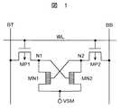
図1は、本発明のメモリセル部の回路図である。4つのトランジスタの結線等の基本構成はこれまでのものと同様である。そして、本発明の例では、高誘電体膜を、メモリセルのクロスカップルを構成するMOSトランジスタMN1とMN2のゲート絶縁膜に使用している。<Example>
FIG. 1 is a circuit diagram of a memory cell portion of the present invention. The basic configuration such as the connection of the four transistors is the same as the conventional one. In the example of the present invention, the high dielectric film is used as the gate insulating film of the MOS transistors MN1 and MN2 constituting the cross couple of the memory cell.
即ち、nチャネルMOSトランジスタMN1とMN2とが、互いのドレイン端子を相手のゲート端子に接続しており、これらの端子がN1とN2である。ソース端子は共通となりVSMとなっている。端子VSMに対して、端子N1とN2との電位差によって情報を保持する。 That is, the n-channel MOS transistors MN1 and MN2 have their drain terminals connected to the other gate terminal, and these terminals are N1 and N2. The source terminal is common and is VSM. Information is held by the potential difference between the terminals N1 and N2 with respect to the terminal VSM.
尚、4つのトランジスタの導電型を反対導電型となしたメモリセルも本発明として用い得ることは言うまでもない。図2はこの例を示す回路図である。符号等は図1に準じて十分である。以下、メモリセルのクロスカップルを構成するトランジスタを主にnチャネルMOSトランジスタを用いた例で説明するが、逆導電型の場合も同様に実施できる。 Needless to say, a memory cell in which the conductivity types of the four transistors are opposite to each other can also be used in the present invention. FIG. 2 is a circuit diagram showing this example. The reference numerals and the like are sufficient according to FIG. Hereinafter, an example in which an n-channel MOS transistor is mainly used as the transistor constituting the cross couple of the memory cell will be described, but the same can be applied to the case of the reverse conductivity type.
情報保持時において、ワード線WLに接続されたpチャネルMOSトランジスタMP1とMP2はオフしており、この時のリーク電流を負荷素子としてnチャネルMOSトランジスタMN1とMN2とに供給している。pチャネルMOSトランジスタMP1とMP2は、又、情報の読み書きを行う機能を兼ねている。この時は、ワード線電圧を変化させてMP1とMP2をオンさせ、ビット線BT、BBと情報を保持している内部ノードN1、N2とを接続する。 At the time of holding information, the p-channel MOS transistors MP1 and MP2 connected to the word line WL are turned off, and the leakage current at this time is supplied to the n-channel MOS transistors MN1 and MN2 as load elements. The p-channel MOS transistors MP1 and MP2 also have a function of reading and writing information. At this time, the word line voltage is changed to turn on MP1 and MP2, and the bit lines BT and BB are connected to the internal nodes N1 and N2 holding the information.
これらの構成において、nチャネル型MOSトランジスタであるMN1とMN2のみに、前述の高誘電体を用いる。図ではこれを示すために、nチャネル型MOSトランジスタMN1とMN2に対して、従来例を示す図18とは異なる記号を用いている。この高誘電体にはMOSトランジスタのI−V特性がヒステリシス特性を有する誘電体を用いる。当該高誘電体膜の比誘電率としては、5から80程度、より好ましくは、5から30の範囲が好ましい。この履歴としては、概ね50mV以上あることが好ましい。このゲート絶縁膜の厚さは、MOSトランジスタのそれと同等で十分であるが、3nmより10nmの範囲が実際的である。又、pチャネル型MOSトランジスタを用いたメモリセルの場合も、前述したように同様に実施できる。 In these configurations, the above-described high dielectric is used only for MN1 and MN2 which are n-channel MOS transistors. In the figure, in order to indicate this, symbols different from those in FIG. 18 showing the conventional example are used for the n-channel MOS transistors MN1 and MN2. As this high dielectric material, a dielectric material having a hysteresis characteristic in the IV characteristics of the MOS transistor is used. The relative dielectric constant of the high dielectric film is preferably about 5 to 80, more preferably 5 to 30. The history is preferably approximately 50 mV or more. The thickness of the gate insulating film is sufficient to be equivalent to that of the MOS transistor, but a range of 3 nm to 10 nm is practical. The memory cell using a p-channel MOS transistor can be similarly implemented as described above.
尚、このメモリセル用の高誘電体膜は、周辺回路や同じチップ上のプロセッサなどを構成するCMOSと同じ材料を基本に構成されている。これらとの違いは、膜厚や動作電圧、或いは形成条件などである。高誘電体膜の材料の代表的な例をあげれば、Al2O3、Ta2O5、HfO2、ZrO2、Nb2O5,Y2O3,La2O3、Si3N4,SiONなどを挙げることが出来る。Note that the high dielectric film for the memory cell is basically made of the same material as the CMOS constituting the peripheral circuit and the processor on the same chip. The difference from these is the film thickness, the operating voltage, or the formation conditions. Typical examples of the material of the high dielectric film include Al2 O3 , Ta2 O5 , HfO2 , ZrO2 , Nb2 O5 , Y2 O3 , La2 O3 , and Si3 N4. , SiON and the like.
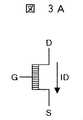
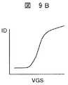
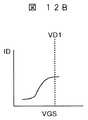
図3A及び図3Bを用いて、図1の実施例に用いる高誘電体膜を用いたnチャネル型MOSトランジスタの動作を説明する。図3Aは、nチャネル型MOSトランジスタの回路的構成図である。図に示すように、nチャネル型MOSトランジスタには、ソース端子Sとゲート端子Gとドレイン端子Dとがある。ソース端子Sとゲート端子Gの電圧差VGSに応じて、ドレイン電流IDが変化する。この場合のI−V特性を図3Bに示す。横軸は電圧、縦軸は電流である。ここで特徴的なことは、電位差VGSを低い電圧から高い電圧に変化させる時と、逆に高い電圧から低い電圧に変化させる時に、ドレイン電流IDのVGS依存性が異なることである。即ち、VGSを低い電圧から高い電圧に変化させる時は、ドレイン電流IDとして、しきい電圧(VT)を定義する電流(IVT)で見てみると、その電圧はV1である。一方、VGSを高い電圧から低い電圧に変化させる時は、IVTでの電圧はV2である。ここで、V1の方がV2よりも高い。IVTの時のVGSの電圧値をもってこのトランジスタのしきい値電圧と定義すると、VGSを低い電圧から高い電圧に変化させる時はしきい値電圧が高く、VGSを高い電圧から低い電圧に変化させる時はしきい値電圧が低い。The operation of the n-channel MOS transistor using the high dielectric film used in the embodiment of FIG. 1 will be described with reference to FIGS. 3A and 3B. FIG. 3A is a circuit configuration diagram of an n-channel MOS transistor. As shown in the figure, the n-channel MOS transistor has a source terminal S, a gate terminal G, and a drain terminal D. The drain current ID changes according to the voltage difference VGS between the source terminal S and the gate terminal G. The IV characteristics in this case are shown in FIG. 3B. The horizontal axis is voltage, and the vertical axis is current. What is characteristic here is that the VGS dependency of the drain current ID differs when the potential difference VGS is changed from a low voltage to a high voltage, and conversely when the potential difference VGS is changed from a high voltage to a low voltage. That is, when VGS is changed from a low voltage to a high voltage, the drain current ID is V1 when viewed from a current (IVT) that defines a threshold voltage (VT ). On the other hand, when VGS is changed from a high voltage to a low voltage, the voltage at IVT is V2. Here, V1 is higher than V2. If the voltage value of VGS at the time of IVT is defined as the threshold voltage of this transistor, the threshold voltage is high when VGS is changed from a low voltage to a high voltage, and the VGS is changed from a high voltage to a low voltage. Has a low threshold voltage.
これを図1に戻って見ると、次の利点がある。図18、図19A、19Bに倣って、端子N1が高電圧、N2が低電圧とする。nチャネル型MOSトランジスタMN1のゲート電圧はN2で低いことになり、nチャネル型MOSトランジスタMN2のゲート電圧は端子N1で高いことになる。これの安定性を考えて見ると、不安定差が増すとは、この端子N1と端子N2の電圧が逆転する方向へ動くことである。即ち、端子N1は高電圧から低電圧へ、端子N2は低電圧から高電圧へとなる。しかしながら、端子N1がゲートに入力しているnチャネル型MOSトランジスタMN2は、高電圧から低電圧への動きであるからしきい値電圧が低い。即ち、なかなかオフしない。よって、端子N2の低電圧から高電圧へ移行を抑えることになる。同様に、端子N2がゲートに入力しているnチャネル型MOSトランジスタMN1は、低電圧から高電圧への動きであるからしきい値電圧が高い。即ち、なかなかオンしない。よって、N1の高電圧から低電圧へ移行を抑えることになる。このように本発明によれば、メモリセルの安定性が増す。 Looking back to FIG. 1, there are the following advantages. 18, 19 </ b> A, and 19 </ b> B, the terminal N <b> 1 is a high voltage and the N <b> 2 is a low voltage. The gate voltage of the n-channel MOS transistor MN1 is low at N2, and the gate voltage of the n-channel MOS transistor MN2 is high at the terminal N1. Considering this stability, the increase in the instability difference means that the voltages at the terminals N1 and N2 move in the reverse direction. That is, the terminal N1 changes from a high voltage to a low voltage, and the terminal N2 changes from a low voltage to a high voltage. However, the threshold voltage of the n-channel MOS transistor MN2 whose terminal N1 is input to the gate is low because it moves from a high voltage to a low voltage. That is, it does not readily turn off. Therefore, the transition from the low voltage to the high voltage at the terminal N2 is suppressed. Similarly, the n-channel MOS transistor MN1 whose terminal N2 is input to the gate has a high threshold voltage because it moves from a low voltage to a high voltage. That is, it does not turn on easily. Therefore, the transition from the high voltage N1 to the low voltage is suppressed. Thus, according to the present invention, the stability of the memory cell is increased.
これによって、図18の実施例では、プロセス変動、温度変動を考慮すると、仮想的な電流IP1は仮想的な電流IN1よりも2桁大きくなければならなかったが、本発明を用いれば、1桁以内へと改善されるのである。仮想的な電流IN1より大きな仮想的な電流IP1の値が、待機時の電力増大を招いていたが、これが大幅に改善されたことになる。 Accordingly, in the embodiment of FIG. 18, the virtual current IP1 has to be two orders of magnitude larger than the virtual current IN1 in consideration of process fluctuations and temperature fluctuations. It is improved within. The value of the virtual current IP1 that is larger than the virtual current IN1 has led to an increase in standby power, which is a significant improvement.
図4は、図1で示したメモリセルを用いたSRAMの例の主要部回路のブロック図である。図5は、図6のブロック図に示された構成の回路例を示す図である。回路例自体は、本発明に関わるMOSトランジスタの具体的材料構成が異なるのみで、通例の通りであるので、詳細説明は省略する。 FIG. 4 is a block diagram of a main circuit of an example of an SRAM using the memory cell shown in FIG. FIG. 5 is a diagram showing a circuit example of the configuration shown in the block diagram of FIG. Since the circuit example itself is the same as that of the MOS transistor according to the present invention except for the specific material configuration, detailed description thereof will be omitted.
図において、MAの領域がメモリアレー部である。図1Aで示したメモリセルが、MCであり、ワード線WL0〜WLnと、ビット線BT0、BB0、BT1、BB1〜とで選択される。ビット線には、プリチャージとイコライズを行うPEが接続し、信号EQで制御される。又、信号YSRで制御され読み出し時にビット線をセンスアンプSAと接続したり、信号YSWで制御され書き込み時にデータを転送したりする回路YSが接続されている。信号CONTはセンスアンプの制御信号である。DECは、制御信号やアドレス信号ADDによって所望のワード線などを選択する回路ブロックであり、ブロックWAは、アドレスやデータ入力信号であるDINに従って、図には示していないがライトアンプを用いてビット線を駆動したり、センスアンプを起動したり、データを増幅したり出力信号DOUTへデータを送る回路ブロックである。 In the figure, the area of MA is a memory array section. The memory cell shown in FIG. 1A is MC, and is selected by the word lines WL0 to WLn and the bit lines BT0, BB0, BT1, and BB1. A PE that performs precharging and equalization is connected to the bit line and is controlled by a signal EQ. A circuit YS is connected which is controlled by the signal YSR and connects the bit line to the sense amplifier SA at the time of reading, and which is controlled by the signal YSW and transfers data at the time of writing. The signal CONT is a control signal for the sense amplifier. DEC is a circuit block that selects a desired word line or the like by a control signal or an address signal ADD. A block WA is a bit that uses a write amplifier (not shown) according to an address or a data input signal DIN. This circuit block drives a line, activates a sense amplifier, amplifies data, and sends data to an output signal DOUT.
図5において、本発明ではメモリセルアレー部MAにおいて、そのメモリセル中の、クロスカップルを構成する、例えばnチャネル型MOSトランジスタのゲート絶縁膜として、V−I特性に履歴を有する高誘電膜を用いる。他の部分のCMOSにも高誘電膜を使い得るが、この部分の履歴は動作上、無視できる大きさとしている。勿論、メモリセルアレー部MA領域以外の領域でのMOSトランジスタのゲート絶縁膜に、メモリセルアレー部MA領域でのMOSトランジスタのゲート絶縁膜である高誘電体膜以外の絶縁物層を用いることも任意であるが、両者を同じ材料で構成することが製造上の観点から有用である。更に、今後CMOSにおいて65nm以降、ゲート絶縁膜として高誘電体膜の導入が目論まれている。従って、こうした高誘電体膜を、メモリアレー部でのゲート絶縁膜に対して、同じ材料を用い且つその厚さなどの条件を変更することによって、本発明が実施可能なことは、量産上極めて有用である。 In FIG. 5, in the present invention, in the memory cell array MA, a high dielectric film having a history in VI characteristics is used as a gate insulating film of, for example, an n-channel MOS transistor that forms a cross couple in the memory cell. Use. A high dielectric film can be used for other portions of the CMOS, but the history of this portion is negligible in operation. Of course, an insulating layer other than the high dielectric film that is the gate insulating film of the MOS transistor in the memory cell array portion MA region may be used for the gate insulating film of the MOS transistor in the region other than the memory cell array portion MA region. Although optional, it is useful from the viewpoint of manufacturing that both are made of the same material. Further, in the future, introduction of a high dielectric film as a gate insulating film is being planned after 65 nm in CMOS. Therefore, the fact that the present invention can be implemented by using such a high dielectric film for the gate insulating film in the memory array portion by using the same material and changing the conditions such as its thickness is extremely important in mass production. Useful.
図7に、図4、5に示したSRAMの回路の動作を示す。各タイムチャートの横軸は時間、縦軸は電圧で、図の左側の符号は、図4、5における各端子の電位を示している。又、図7の上部に示したNOP、READ、及びWRITEの各領域は、各々読出し動作も書込み動作も行っていない場合、読出し動作、及び書込み動作の領域を示している。 FIG. 7 shows the operation of the SRAM circuit shown in FIGS. In each time chart, the horizontal axis represents time, the vertical axis represents voltage, and the symbol on the left side of the figure represents the potential of each terminal in FIGS. Further, the NOP, READ, and WRITE areas shown in the upper part of FIG. 7 indicate the areas of the read operation and the write operation, respectively, when neither the read operation nor the write operation is performed.
読出し動作READも書込み動作WRITEも行っていない場合(NOP)は、プロチャージ・イコライズ制御信号EQはL(低)レベル、読出し用Yスイッチ制御信号YSRはH(高)レベル、書込み用Yスイッチ制御信号YSWはLレベル、センスアンプ制御信号SACはLレベルとなっている。 When neither the read operation READ nor the write operation WRITE is performed (NOP), the procharge / equalize control signal EQ is L (low) level, the read Y switch control signal YSR is H (high) level, and the write Y switch control The signal YSW is at L level and the sense amplifier control signal SAC is at L level.
読出し動作READは次のように行なわれる。アドレス信号或いはクロックが入力されると、デコーダDECによりアドレス信号がデコードされ、一本のワード線WLが選択される。同時にプロチャージ・イコライズ制御信号EQはLレベルからHレベルに、読出し用Yスイッチ制御信号YSRはHレベルからLレベルにそれぞれ遷移する。これにより、ビット線対(BT、BB)とセンスアンプSAが接続され、ビット線対(BT、BB)に微小電圧差が発生する。センスアンプ制御信号SACがLレベルからHレベルに遷移するとセンスアンプSAが活性化し、ビット線対(BT、BB)に発生した微小電圧差が増幅され、読み出されたデータが外部出力DOUTに現れる。 The read operation READ is performed as follows. When an address signal or a clock is input, the address signal is decoded by the decoder DEC, and one word line WL is selected. At the same time, the procharge / equalize control signal EQ changes from the L level to the H level, and the read Y switch control signal YSR changes from the H level to the L level. As a result, the bit line pair (BT, BB) and the sense amplifier SA are connected, and a minute voltage difference is generated between the bit line pair (BT, BB). When the sense amplifier control signal SAC transitions from the L level to the H level, the sense amplifier SA is activated, the minute voltage difference generated in the bit line pair (BT, BB) is amplified, and the read data appears on the external output DOUT. .
一方、書込み動作WRITEは以下となる。アドレス信号或いはクロックが入力されると、デコーダDECによりアドレス信号がデコードされ、一本のワード線WLが選択される。同時にプロチャージ・イコライズ制御信号EQはLレベルからHレベルに、書込み用Yスイッチ制御信号YSWはLレベルからHレベルにそれぞれ遷移する。これにより、ビット線対(BT、BB)とライトアンプが接続され、外部入力DINの信号がライトアンプを解して、ビット線対(BT、BB)に入力される。ビット線対(BT、BB)に入力されたデータが選択されたワード線WLに接続するメモリセルCELに書き込まれる。 On the other hand, the write operation WRITE is as follows. When an address signal or a clock is input, the address signal is decoded by the decoder DEC, and one word line WL is selected. At the same time, the procharge / equalize control signal EQ changes from the L level to the H level, and the write Y switch control signal YSW changes from the L level to the H level. Thereby, the bit line pair (BT, BB) and the write amplifier are connected, and the signal of the external input DIN is input to the bit line pair (BT, BB) via the write amplifier. Data input to the bit line pair (BT, BB) is written into the memory cell CEL connected to the selected word line WL.
図8は、図4、5に示したSRAM回路の他の動作を示す。各記号は図7と同じである。異なる点は、READとWRITE時におけるワード線WLの電圧である。図7では、HレベルがVDDであり、LレベルがVSSであったが、図8では、HレベルがVDDであるが、LレベルがVSSWとVSSよりも高い電圧である。すなわち、ワード線WLが選択された時、VSSと低くはならず、それより高いVSSWとなる。このため、メモリセルMC内のpチャネル型MOSトランジスタが弱くしかオンせず、流れう得る電流が小さい。これは次の利点がある。nチャネル型MOSトランジスタのゲート絶縁膜に本発明では履歴を有する高誘電膜を用いる。これを実現するために、例えば、図6に示したようにこのnチャネル型MOSトランジスタゲート絶縁膜の膜厚は厚いものとなる。このように膜圧を厚くすると一般に電流駆動能力は低下する。これに対応して、pチャネル型MOSトランジスタの電流駆動能力を下げる必要がある。そうしないと、読み出し、又は書き込み動作時に記憶されたデータが破壊されてしまうからである。電流駆動能力を下げるには、より小さなトランジスタサイズ(ゲート幅)を用いることも考えられるが、SRAMは一般に加工技術上最小サイズのトランジスタで作成されるため、もはや、更に小さなトランジスタサイズとは出来ない。この時、本実施例の如く方法を用いれば、pチャネル型MOSトランジスタの電流駆動能力を小さくすることができる。選択時であるワード線WLのLレベルをVSSWとVSSよりも高い電圧とすることで、履歴を有する高誘電膜をゲート絶縁膜に用いたnチャネル型MOSトランジスタに適した電流駆動能力のpチャネル型MOSトランジスタを実現でき、安定動作を図ることができる。尚、図8では、READとWRITE時に同じLレベルVSSWとしたが、これはREADとWRITEとで異なる値とすることで、メモリセルがデータ破壊などを起こさないような安定動作のために、よりトランジスタの特性にあった動作を行なわせることができる。 FIG. 8 shows another operation of the SRAM circuit shown in FIGS. Each symbol is the same as in FIG. The difference is the voltage of the word line WL during READ and WRITE. In FIG. 7, the H level is VDD and the L level is VSS. In FIG. 8, the H level is VDD, but the L level is higher than VSSW and VSS. That is, when the word line WL is selected, it does not become lower than VSS but becomes higher VSS. For this reason, the p-channel MOS transistor in the memory cell MC is turned on only weakly, and the current that can flow is small. This has the following advantages. In the present invention, a high dielectric film having a history is used for the gate insulating film of the n-channel MOS transistor. In order to realize this, for example, as shown in FIG. 6, the thickness of the n-channel MOS transistor gate insulating film is increased. When the film pressure is increased as described above, the current driving capability generally decreases. Correspondingly, it is necessary to reduce the current drive capability of the p-channel MOS transistor. Otherwise, the data stored during the read or write operation will be destroyed. In order to reduce the current driving capability, it is conceivable to use a smaller transistor size (gate width). However, since an SRAM is generally made of a transistor having the smallest size in terms of processing technology, it can no longer be made smaller. . At this time, if the method as in this embodiment is used, the current drive capability of the p-channel MOS transistor can be reduced. By selecting the L level of the word line WL at the time of selection higher than VSSW and VSS, a p-channel having a current driving capability suitable for an n-channel MOS transistor using a high dielectric film having a history as a gate insulating film A type MOS transistor can be realized and stable operation can be achieved. In FIG. 8, the same L level VSSW is set for READ and WRITE. However, by setting different values for READ and WRITE, the memory cell can be operated more stably for preventing data destruction and the like. An operation suited to the characteristics of the transistor can be performed.
これまで、一般的なSRAMの動作を説明してきたが、次に、本発明のMOSトランジスタの具体的構成とこれに基づく動作上の利点について説明する。図6は、図3Aで示した例のMOSトランジスタの主要部断面を模式的に示した図である。図において、メモリアレーMA及びMA以外の表示は各々SRAMを構成しているのメモリアレー領域と、それ以外の領域でのMOSトランジスタの基本構成を示している。両領域を並置して示しているが、必ずしも並置する構成を例示せんとするものではなく、各種MOSトランジスタの構成の比較を例示するものである。各MOSトランジスタの基本構成は通例のものと同様である。符号100は半導体基板、101、111はn型不純物領域、102、112はp型不純物領域、103、113はMOSトランジスタのソース或いはドレインとなるp型高濃度不純物領域、104、114はMOSトランジスタのソース或いはドレインとなるn型高濃度不純物領域、105、106、115、116はゲート絶縁膜、107、108、117、118はゲート電極である。図の上部にその下部に示すMOSトランジスタのタイプ(nMOS、pMOS)並びにこれらの各MOSトランジスタに対応するゲート絶縁膜の厚さの比較を示した。ゲート絶縁膜の「厚」、「薄」はこれらの相互の厚さの比較を示す。 The operation of a general SRAM has been described so far. Next, the specific configuration of the MOS transistor of the present invention and the operational advantages based on this will be described. FIG. 6 is a diagram schematically showing a cross section of the main part of the MOS transistor of the example shown in FIG. 3A. In the figure, the displays other than the memory arrays MA and MA indicate the basic configuration of the MOS transistors in the memory array area constituting the SRAM and other areas. Although both regions are shown in juxtaposition, the configuration of juxtaposing them is not necessarily illustrated, but a comparison of configurations of various MOS transistors is illustrated. The basic configuration of each MOS transistor is the same as the usual one. Reference numeral 100 is a semiconductor substrate, 101 and 111 are n-type impurity regions, 102 and 112 are p-type impurity regions, 103 and 113 are p-type high-concentration impurity regions that serve as the source or drain of a MOS transistor, and 104 and 114 are MOS transistor transistors. An n-type high-concentration impurity region serving as a source or drain, 105, 106, 115, and 116 are gate insulating films, and 107, 108, 117, and 118 are gate electrodes. In the upper part of the figure, the MOS transistor type (nMOS, pMOS) shown in the lower part and the thickness of the gate insulating film corresponding to each of these MOS transistors are shown. The “thickness” and “thin” of the gate insulating film indicate a comparison between these thicknesses.
この実施例の特徴は、メモリアレーMAの領域と、それ以外の領域におけるnチャネルMOSトランジスタのゲート絶縁膜の厚さの差にある。両方のトランジスタ共に高誘電膜を使っているが、ARRの領域のnMOSトランジスタのゲート絶縁膜の厚さの方が、それ以外の領域のnMOSトランジスタのゲート絶縁膜の厚さよりも厚い。一方、pMOSトランジスタのゲート絶縁膜の厚さは同じである。例えば、薄い方の厚さが、2nm程度であるのに対して、厚い方は4nm〜6nm程度である。このように厚くすることで、MOSのV−I特性に履歴を持つようになる。 The feature of this embodiment is the difference in the thickness of the gate insulating film of the n-channel MOS transistor in the memory array MA region and other regions. Although both transistors use a high dielectric film, the thickness of the gate insulating film of the nMOS transistor in the ARR region is thicker than the thickness of the gate insulating film of the nMOS transistor in the other region. On the other hand, the thickness of the gate insulating film of the pMOS transistor is the same. For example, the thickness of the thinner one is about 2 nm, while the thicker one is about 4 to 6 nm. By increasing the thickness in this way, the MOS VI has a history.
こうした特性比較を図9A及び図9Bに示した。横軸が電圧、縦軸はドレイン電流である。図9Aはゲート絶縁膜が厚い膜の場合であり、図9Bは薄い膜の場合である。図9Aの例は図3Bでの説明と同様で、ゲート電圧VGSを上昇させる場合と、下降させる場合とでその電流特性が異なる。これによって、これまで説明して来たようにSRAMの情報保持の安定性を増すことができる。 Such a characteristic comparison is shown in FIGS. 9A and 9B. The horizontal axis is voltage, and the vertical axis is drain current. FIG. 9A shows a case where the gate insulating film is a thick film, and FIG. 9B shows a case where the gate insulating film is a thin film. The example of FIG. 9A is the same as that described with reference to FIG. 3B, and the current characteristics differ between when the gate voltage VGS is raised and when it is lowered. As a result, the stability of information retention in the SRAM can be increased as described above.
一方、図9Bに示すように、ゲート絶縁膜が薄い膜の場合にはこの履歴は見られない。こうした特性は、論理回路やアンプ回路が正常に動作するのに必須である。例えば、論理回路に図9Aのような素子を使うと出力の立ち上がり特性と、立ち下がり特性が異なることになってしまい、ランダムに動作する各回路間のタイミング設計が不可能となる。このため、このような場所には、V−I特性に履歴の無い膜を使うのが必須である。通常、高誘電膜のCMOS回路への適用に当たっては、履歴の無い膜を作るのに努力が払われる。 On the other hand, as shown in FIG. 9B, this history is not seen when the gate insulating film is a thin film. Such characteristics are essential for the normal operation of the logic circuit and the amplifier circuit. For example, if an element as shown in FIG. 9A is used in the logic circuit, the output rising characteristics and the falling characteristics will be different, making it impossible to design the timing between the randomly operating circuits. For this reason, it is essential to use a film having no history in the VI characteristic in such a place. Usually, in applying a high dielectric film to a CMOS circuit, an effort is made to produce a film having no history.
発明者等は、SRAMのメモリセル部分にはこの考えを外すことで新たな価値ができるのを見出した。即ち、履歴を利用して情報保持を安定化させることである。 The inventors have found that a new value can be obtained by removing this idea from the memory cell portion of the SRAM. That is, it is to stabilize information holding using a history.
図6、図9A、図9Bを用いて膜厚を変える例を示したが、他に高誘電体をゲート絶縁膜に使うCMOSにおいて、この膜が前記履歴を持たないように行っているプロセス処理を、SRAMのメモリセル部分では省くことでもこれを達成できる。 Although the example of changing the film thickness using FIGS. 6, 9A, and 9B has been shown, in the CMOS using a high dielectric as the gate insulating film, the process is performed so that the film does not have the history. This can also be achieved by omitting the memory cell portion of the SRAM.
次に、ゲート絶縁膜の膜厚を変えないで、履歴が欲しいRAM部では高い電圧を印可し、履歴を小さくしたい論理回路では低い電圧を与えることで、本発明の所望の性能を実現する方法を説明する。 Next, without changing the film thickness of the gate insulating film, a high voltage is applied to the RAM portion where the history is desired, and a low voltage is applied to the logic circuit where the history is desired to be reduced, thereby realizing the desired performance of the present invention. Will be explained.
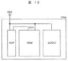
図10は、SRAMのメモリセル部分のみに前記履歴を持つトランジスタを実現する他の実施例を例示するブロック構成図である。ここでは、メモリセル部分(RAM)の印可電圧VD1を論理回路(LOGIC)やメモリ周辺回路の印可電圧VD2よりも高く設定している。この高電圧VD1は、印可電圧VD2より、高電圧発生回路VDPで発生させている。符号VDPは良く知られているチャージポンプ回路、及び様々な改良回路で構成する。高電圧VD1が、例えば1V程度であるのに対して、印可電圧VD2は例えば、2.5V程度である。 FIG. 10 is a block diagram illustrating another embodiment for realizing the transistor having the history only in the memory cell portion of the SRAM. Here, the applied voltage VD1 of the memory cell portion (RAM) is set higher than the applied voltage VD2 of the logic circuit (LOGIC) or the memory peripheral circuit. The high voltage VD1 is generated from the applied voltage VD2 by the high voltage generation circuit VDP. The symbol VDP comprises a well-known charge pump circuit and various improved circuits. The high voltage VD1 is about 1V, for example, while the applied voltage VD2 is about 2.5V, for example.
図11は、このような電圧を印可する他の実施例を例示するブロック構成図である。外部入出力回路IOが配置されているが、一般に、ここの電源電圧は論理回路よりも高い。この実施例ではこれを利用しており、印可電圧VD2は、外部入出力回路IOに印可され、これは論理回路LOGICに印可されている電源VD1の電圧よりも一般に高い。これを利用して、RAMにこの電圧を印可し、SRAMのメモリセルの制御電圧とする。 FIG. 11 is a block diagram illustrating another embodiment for applying such a voltage. Although the external input / output circuit IO is arranged, the power supply voltage here is generally higher than that of the logic circuit. In this embodiment, this is utilized, and the applied voltage VD2 is applied to the external input / output circuit IO, which is generally higher than the voltage of the power supply VD1 applied to the logic circuit LOGIC. Using this, this voltage is applied to the RAM, and used as the control voltage of the SRAM memory cell.
このようにSRAMのメモリセルの部分のみ高い電圧を印可することにより、膜厚を変えなくても履歴のある特性を見ることが出来る。この場合の特性例を図12A及び図12Bに示す。横軸が電圧、縦軸はドレイン電流である。図12Aに示すように、高い電圧である印可電圧VD2までのドレイン電流IDとVGSの関係では、履歴が現われる。一方、図12Bに示すように、電源電圧VD1と低い電圧では、履歴は無視することができる。これにより、履歴が欲しいRAM部では高い電圧を印可し、履歴を小さくしたい論理回路では低い電圧を与えることで所望の性能を実現できる。尚、これまでの説明では、ゲート絶縁膜の膜厚は同じとしたが、この膜厚も変えると共に前記電圧印加の手段を合せて用いることにより、より安定な動作を得ることができる。即ち、膜厚を厚くし、且つ高い電圧を印可するのである。尚、pチャネルMOSトランジスタを、nチャネルMOSトランジスタの上部に作ることもできる。 In this way, by applying a high voltage only to the memory cell portion of the SRAM, it is possible to see a characteristic having a history without changing the film thickness. Examples of characteristics in this case are shown in FIGS. 12A and 12B. The horizontal axis is voltage, and the vertical axis is drain current. As shown in FIG. 12A, a history appears in the relationship between the drain current ID and VGS up to the applied voltage VD2, which is a high voltage. On the other hand, as shown in FIG. 12B, the history can be ignored at the power supply voltage VD1 and a low voltage. Thus, a desired performance can be realized by applying a high voltage to a RAM unit that wants a history and applying a low voltage to a logic circuit that wants to reduce the history. In the description so far, the thickness of the gate insulating film is the same. However, by changing the thickness and using the voltage applying means together, a more stable operation can be obtained. That is, the film thickness is increased and a high voltage is applied. A p-channel MOS transistor can also be formed on top of the n-channel MOS transistor.
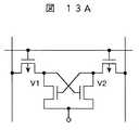
図13A、13B及び図14A、14Bの各図をもって、本発明の効果を、SRAMの特性から比較検討する。図13Aは従来のSRAMの回路図、図13Bは、図13A中の2つのノードをV1とV2と表し、ノードV1に対するノードV2の電圧特性と、ノードV2に対するノードV1の電圧特性とを同時に書いたものである。この時、2つの曲線で囲まれる部分、図13BのLOで示した部分が大きい程、安定であることを示している。即ち、図13Aに示す従来のSRAMでは、ノードV1に対するノードV2の電圧特性と、ノードV2に対するノードV1の電圧特性の依存性の差から履歴が生まれ、これが情報保持を表している。しかしながら、ノードV1に対するノードV2の電圧特性は、ノードV1を上昇させる時と、下降させる時とは一致する。これは、ノードV2に対するノードV1の電圧特性も同様である。 13A and 13B and FIGS. 14A and 14B, the effects of the present invention will be compared and examined from the characteristics of the SRAM. FIG. 13A is a circuit diagram of a conventional SRAM, and FIG. 13B represents two nodes in FIG. 13A as V1 and V2, and simultaneously writes the voltage characteristics of the node V2 with respect to the node V1 and the voltage characteristics of the node V1 with respect to the node V2. It is a thing. At this time, the larger the portion surrounded by two curves, the portion indicated by LO in FIG. 13B, the more stable it is. That is, in the conventional SRAM shown in FIG. 13A, a history is generated from the difference in dependency between the voltage characteristic of the node V2 with respect to the node V1 and the voltage characteristic of the node V1 with respect to the node V2, and this represents information retention. However, the voltage characteristics of the node V2 with respect to the node V1 coincide with when the node V1 is raised and when it is lowered. The same applies to the voltage characteristic of the node V1 with respect to the node V2.
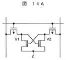
一方、図14Aは本発明のSRAMの回路図、図14Bは、図14A中の2つのノードをV1とV2と表し、ノードV1に対するノードV2の電圧特性と、ノードV2に対するノードV1の電圧特性とを同時に書いたものである。 On the other hand, FIG. 14A is a circuit diagram of the SRAM of the present invention, and FIG. 14B shows two nodes in FIG. 14A as V1 and V2, and the voltage characteristics of the node V2 with respect to the node V1 and the voltage characteristics of the node V1 with respect to the node V2. Is written at the same time.
本発明の場合、ノードV1に対するノードV2の電圧特性は、ノードV1を上昇させる時と、下降させる時とでは異なり、又、ノードV2に対するノードV1の電圧特性も同様で、ノードV2を上昇させる時と、下降させる時とでは異なる。この結果、安定度を示す図10Bに示される領域LNは、従来例の領域LOよりも大きくなる。このように本発明はメモリセルの安定性を高めることができる。このため、低電力としてもメモリセルの安定性が損なわれることはない。 In the case of the present invention, the voltage characteristic of the node V2 with respect to the node V1 is different between when the node V1 is raised and when it is lowered, and the voltage characteristic of the node V1 with respect to the node V2 is the same, and when the node V2 is raised. And when it is lowered. As a result, the region LN shown in FIG. 10B showing the stability is larger than the region LO of the conventional example. Thus, the present invention can increase the stability of the memory cell. For this reason, the stability of the memory cell is not impaired even when the power is low.
次に、本発明に縦型MOSトランジスタを用いた構造について説明する。メモリセルを構成する前記第3及び第4のMOSトランジスタ(即ち、転送MOS)、例えば前記pチャネルMOSトランジスタ(MP1、MP2)を半導体基板上に積層可能な縦型MOSトランジスタで構成することは、占有面積の縮小に極めて有用である。ここで、縦型MOSトランジスタ自体の基本構成はこれまで知られたもので十分である。そして、本発明では、メモリセルのクロスカップルを構成するMOSトランジスタのゲート絶縁膜を前述の通りの強誘電体層で形成する。尚、縦型MOSトランジスタとは、チャネルの長手方向、即ち、キャリアの流れる方向が半導体層の積層を行う基板に対して交差する方向、通例垂直に形成されたMOSトランジスタのことである。 Next, a structure using a vertical MOS transistor in the present invention will be described. The third and fourth MOS transistors (that is, transfer MOS) constituting the memory cell, for example, the p-channel MOS transistors (MP1, MP2) are constituted by vertical MOS transistors that can be stacked on a semiconductor substrate. This is extremely useful for reducing the occupied area. Here, the basic configuration of the vertical MOS transistor itself is sufficient as it has been known so far. In the present invention, the gate insulating film of the MOS transistor constituting the cross couple of the memory cell is formed of the ferroelectric layer as described above. Note that a vertical MOS transistor is a MOS transistor formed in the longitudinal direction of a channel, that is, a direction in which carriers flow in a direction intersecting with a substrate on which semiconductor layers are stacked, usually perpendicularly.
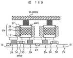
図15A及び図15Bにこうした縦型MOSトランジスタを用いる場合の平面レイアウトを示す。図15Aは積層体の上層部、図15Bは下層部を示す。図16Aは図15A、15Bでの線A−A’に沿った断面図、図16Bは図15A、15Bでの線B−B’に沿った断面図である。尚、回路構成自体は既に説明したものと同様である。 FIGS. 15A and 15B show a planar layout in the case of using such a vertical MOS transistor. FIG. 15A shows the upper layer portion of the laminate, and FIG. 15B shows the lower layer portion. 16A is a cross-sectional view taken along line A-A 'in FIGS. 15A and 15B, and FIG. 16B is a cross-sectional view taken along line B-B' in FIGS. 15A and 15B. The circuit configuration itself is the same as that already described.
各図において、MN1及びMN2と表示した部分は、半導体基板部に形成されたnチャネルMOSトタンジスタの部分を示す。符号10、15は配線、11、13、17、18は各々コンタクトホール、12、16はゲート電極、14は活性領域である。断面図に即せば、符号19は下部の半導体層、20は中間半導体層、21は上部半導体層、22はゲート絶縁膜、23は素子分離領域、24はp型ウエル、25はp+型ウエル、26、27、28はプラグ、29はn+型半導体領域(ソース、ドレインとなる)、30はn−型半導体領域である。In each figure, the portions indicated as MN1 and MN2 indicate portions of n-channel MOS transistors formed in the semiconductor substrate portion.
pチャネルMOSトランジスタ(MP1、MP2)は、下部半導体層19(ドレイン)、中間半導体層20、及び上部半導体層21(ソース)を積層した四角柱状の積層体SVと、この積層体SVの側壁に配置されたゲート絶縁膜22を介して形成されたゲート電極16とで構成される。 The p-channel MOS transistors (MP1, MP2) include a quadrangular columnar stacked body SV in which a lower semiconductor layer 19 (drain), an
pチャネルMOSトランジスタ(MP1、MP2)が、縦型MOSトランジスタで構成されることによって、いわゆるウエル分離領域が不要となる。この為、メモリセルMCを構成するすべてのMOSトランジスタを半導体基板上に形成した場合と比較して、メモリセルMCを小型化することが出来る。又、pチャネルMOSトランジスタ(MP1、MP2)を、半導体薄膜を用いた薄型トランジスタ(TFT)で構成し、前記nチャネルMOSトランジスタに積層して、本発明を構成しても、同様の効果を得ることが出来る。 Since the p-channel MOS transistors (MP1, MP2) are formed of vertical MOS transistors, so-called well isolation regions are not required. Therefore, the memory cell MC can be reduced in size compared to the case where all the MOS transistors constituting the memory cell MC are formed on the semiconductor substrate. Further, even if the p-channel MOS transistors (MP1, MP2) are constituted by thin transistors (TFTs) using a semiconductor thin film and stacked on the n-channel MOS transistors, the same effect can be obtained. I can do it.
図17に、本発明のSRAMをマイコンに適用した例を、ブロック図として例示する。チップ基板308に搭載されたCPU306に対して、SRAMメモリアレイ部303、不揮発性メモリアレイ部305が配置される。これらの両アレイ間にメモリ制御回路304、バスコントロール307、機能回路ブロック308がこの周辺に配置される。尚、符号327はIO、322は電源回路、321はPLLである。上記SRAMメモリアレイ部303に本発明のSRAMが用いられる。尚、各部の役割自体は通例のものと同様であるので、その詳細な説明は省略する。 FIG. 17 illustrates, as a block diagram, an example in which the SRAM of the present invention is applied to a microcomputer. An SRAM
以上説明したように、本発明を用いれば、オンチップSRAMに関し、小面積且つ低リークなSRAMを実現できる。この為、本発明のSRAMを、モバイル機器LSIに用いれば、高性能、且つ低待機電力とできる。 As described above, when the present invention is used, a small area and low leak SRAM can be realized with respect to the on-chip SRAM. For this reason, if the SRAM of the present invention is used in a mobile device LSI, high performance and low standby power can be achieved.
10:配線、11:コンタクトホール、12:ゲート電極、13:コンタクトホール、14:活性領域、15:配線、16:ゲート電極、17、18:コンタクトホール、19:下部半導体層、20:中間半導体層、21:上部半導体層、22:ゲート絶縁膜、23:素子分離領域、24:p型ウエル、25:p+型半導体領域、26、27、28:プラグ、29:n+型半導体領域(ソース、ドレイン)、30:n−型半導体領域、100:基板、101、111:n型領域、102、112:p型領域、103、113:p+型領域、104、114:n+型領域、105、106、115、116:ゲート絶縁膜、107、108、117、118:ゲート、308:基板、303:SRAMメモリアレイ、304:メモリ制御回路、305:不揮発性メモリアレイ、306:CPU、307:バスコントロール、308:機能回路ブロック、321:PLL、322:電源回路、327:IO。10: wiring, 11: contact hole, 12: gate electrode, 13: contact hole, 14: active region, 15: wiring, 16: gate electrode, 17, 18: contact hole, 19: lower semiconductor layer, 20: intermediate semiconductor Layer: 21: upper semiconductor layer, 22: gate insulating film, 23: element isolation region, 24: p-type well, 25: p+ type semiconductor region, 26, 27, 28: plug, 29: n+ type semiconductor region ( Source, drain), 30: n− type semiconductor region, 100: substrate, 101, 111: n type region, 102, 112: p type region, 103, 113: p+ type region, 104, 114: n+ type region 105, 106, 115, 116: gate insulating film, 107, 108, 117, 118: gate, 308: substrate, 303: SRAM memory array, 304: memory control circuit , 305: non-volatile memory array, 306: CPU, 307: bus control, 308: functional circuit blocks, 321: PLL, 322: power circuit, 327: IO.
Claims (17)
Translated fromJapanese前記第1及び第2の絶縁ゲート型電界効果型トランジスタのゲート絶縁膜が、当該絶縁ゲート型電界効果型トランジスタの電圧−電流特性がヒステリシス特性を有する誘電体膜で構成されていることを特徴とする半導体記憶装置。First and second insulated gate field effect transistors each having a first conductivity type channel are arranged such that each drain terminal is connected to the other gate terminal and each source terminal is connected in common. And a memory having one terminal of each of third and fourth insulated gate field effect transistors each having a channel of the second conductivity type connected to each of two output ends of the cross couple. Have cells,
The gate insulating film of the first and second insulated gate field effect transistors is formed of a dielectric film whose voltage-current characteristics of the insulated gate field effect transistors have hysteresis characteristics. A semiconductor memory device.
前記メモリセル及び前記論理回路とが有する絶縁ゲート型電界効果型トランジスタのゲート絶縁膜は高誘電体膜で形成され、且つ
前記メモリセルは、第1の導電型のチャネルを有する、第1及び第2の絶縁ゲート型電界効果型トランジスタが、互いのドレイン端子が相手のゲート端子に接続され、互いのソース端子が共通に接続されて配されたクロスカップルと、当該クロスカップルの2つの出力端の各々に、第2の導電型のチャネルを有する、第3及び第4の絶縁ゲート型電界効果型トランジスタの一方の端子が各々接続されたメモリセルであり、
前記メモリセルへの印加電圧が、当該メモリセルの前記第1及び第2の絶縁ゲート型電界効果型トランジスタのゲート絶縁膜を構成する高誘電体膜が、当該絶縁ゲート型電界効果型トランジスタの電圧−電流特性がヒステリシス特性を有する電圧と設定されたことを特徴とする半導体記憶装置。Having at least a memory cell and a logic circuit;
The gate insulating film of the insulated gate field effect transistor included in the memory cell and the logic circuit is formed of a high dielectric film, and the memory cell has a first conductivity type channel, Two insulated gate field effect transistors, each having a drain couple connected to the other gate terminal and a common source terminal connected to each other, and two output terminals of the cross couple. Each of the memory cells has a second conductivity type channel and is connected to one terminal of each of the third and fourth insulated gate field effect transistors.
The voltage applied to the memory cell is such that the high dielectric film constituting the gate insulating film of the first and second insulated gate field effect transistors of the memory cell is the voltage of the insulated gate field effect transistor. A semiconductor memory device, wherein the current characteristic is set to a voltage having a hysteresis characteristic.
前記論理回路とが有する絶縁ゲート型電界効果型トランジスタのゲート絶縁膜を形成する高誘電体膜は、当該絶縁ゲート型電界効果型トランジスタの電圧−電流特性がヒステリシス特性を有さない電圧と設定されていることを特徴とする請求項6に記載の半導体記憶装置。The high dielectric film forming the gate insulating film of the insulated gate field effect transistor included in the memory cell is set such that the voltage-current characteristic of the insulated gate field effect transistor has a hysteresis characteristic,
The high dielectric film forming the gate insulating film of the insulated gate field effect transistor included in the logic circuit is set so that the voltage-current characteristic of the insulated gate field effect transistor does not have a hysteresis characteristic. The semiconductor memory device according to claim 6.
前記メモリセルの有する高誘電体膜の膜厚が前記論理回路の有する高誘電体膜の膜厚より厚いことを特徴とする請求項8に記載の半導体記憶装置。The high dielectric film of the memory cell is formed of the same material as the high dielectric film of the logic circuit, and the high dielectric film of the logic circuit has a film thickness of the high dielectric film of the memory cell. 9. The semiconductor memory device according to claim 8, wherein the semiconductor memory device is thicker than the thickness of the semiconductor memory device.
前記第1及び第2の絶縁ゲート型電界効果型トランジスタのゲート絶縁膜が、当該絶縁ゲート型電界効果型トランジスタの電圧−電流特性がヒステリシス特性を有する誘電体膜で構成されていることを特徴とする半導体記憶装置。First and second insulated gate field effect transistors each having a first conductivity type channel are arranged such that each drain terminal is connected to the other gate terminal and each source terminal is connected in common. And a static coupling in which one terminal of each of third and fourth insulated gate field effect transistors having a channel of the second conductivity type is connected to each of two output ends of the cross couple. Random access memory cells,
The gate insulating film of the first and second insulated gate field effect transistors is formed of a dielectric film whose voltage-current characteristics of the insulated gate field effect transistors have hysteresis characteristics. A semiconductor memory device.
Priority Applications (1)
| Application Number | Priority Date | Filing Date | Title |
|---|---|---|---|
| JP2004118709AJP2005303111A (en) | 2004-04-14 | 2004-04-14 | Semiconductor memory device |
Applications Claiming Priority (1)
| Application Number | Priority Date | Filing Date | Title |
|---|---|---|---|
| JP2004118709AJP2005303111A (en) | 2004-04-14 | 2004-04-14 | Semiconductor memory device |
Publications (1)
| Publication Number | Publication Date |
|---|---|
| JP2005303111Atrue JP2005303111A (en) | 2005-10-27 |
Family
ID=35334230
Family Applications (1)
| Application Number | Title | Priority Date | Filing Date |
|---|---|---|---|
| JP2004118709APendingJP2005303111A (en) | 2004-04-14 | 2004-04-14 | Semiconductor memory device |
Country Status (1)
| Country | Link |
|---|---|
| JP (1) | JP2005303111A (en) |
Cited By (5)
| Publication number | Priority date | Publication date | Assignee | Title |
|---|---|---|---|---|
| JP2010219455A (en)* | 2009-03-19 | 2010-09-30 | National Institute Of Advanced Industrial Science & Technology | Method for manufacturing insulated gate semiconductor device |
| JP2011061110A (en)* | 2009-09-14 | 2011-03-24 | Unisantis Electronics Japan Ltd | Semiconductor memory device |
| JP2013058773A (en)* | 2012-10-26 | 2013-03-28 | Unisantis Electronics Singapore Pte Ltd | Semiconductor device |
| JP2016134184A (en)* | 2015-01-16 | 2016-07-25 | 株式会社東芝 | Semiconductor storage device |
| US10957373B2 (en) | 2018-07-05 | 2021-03-23 | Samsung Electronics Co., Ltd. | Semiconductor memory device |
- 2004
- 2004-04-14JPJP2004118709Apatent/JP2005303111A/enactivePending
Cited By (5)
| Publication number | Priority date | Publication date | Assignee | Title |
|---|---|---|---|---|
| JP2010219455A (en)* | 2009-03-19 | 2010-09-30 | National Institute Of Advanced Industrial Science & Technology | Method for manufacturing insulated gate semiconductor device |
| JP2011061110A (en)* | 2009-09-14 | 2011-03-24 | Unisantis Electronics Japan Ltd | Semiconductor memory device |
| JP2013058773A (en)* | 2012-10-26 | 2013-03-28 | Unisantis Electronics Singapore Pte Ltd | Semiconductor device |
| JP2016134184A (en)* | 2015-01-16 | 2016-07-25 | 株式会社東芝 | Semiconductor storage device |
| US10957373B2 (en) | 2018-07-05 | 2021-03-23 | Samsung Electronics Co., Ltd. | Semiconductor memory device |
Similar Documents
| Publication | Publication Date | Title |
|---|---|---|
| JP6324595B2 (en) | Semiconductor memory device | |
| US8330496B2 (en) | Semiconductor integrated circuit device | |
| US7639525B2 (en) | Semiconductor memory device | |
| US7498637B2 (en) | Semiconductor memory | |
| JP5865421B2 (en) | Semiconductor device | |
| US7764540B2 (en) | Semiconductor memory device | |
| KR101919057B1 (en) | Semiconductor memory device and driving method thereof | |
| JP2005514775A (en) | Memory cell using differential negative resistance field effect transistor | |
| JP2002368135A (en) | Semiconductor storage device | |
| JP2005072599A (en) | Unloaded nmos four transistor dynamic dual vtsram cell | |
| US7180768B2 (en) | Semiconductor memory device including 4TSRAMs | |
| JP2004213722A (en) | Semiconductor storage device and semiconductor integrated circuit device | |
| JP3551468B2 (en) | Operation method of SRAM memory cell | |
| JP2005303111A (en) | Semiconductor memory device | |
| JP4339766B2 (en) | Semiconductor device | |
| JP2008135169A (en) | Semiconductor storage device | |
| JP2011090782A (en) | Semiconductor memory device | |
| CN114883318A (en) | Apparatus including semiconductor layout to mitigate local layout effects | |
| JP2005129109A (en) | Semiconductor memory device | |
| JP2011018438A (en) | Semiconductor device |