Movatterモバイル変換


[0]ホーム

URL:


JP2005286053A - Semiconductor device - Google Patents

Semiconductor device
Download PDF

Info

Publication number
JP2005286053A
JP2005286053AJP2004096915AJP2004096915AJP2005286053AJP 2005286053 AJP2005286053 AJP 2005286053AJP 2004096915 AJP2004096915 AJP 2004096915AJP 2004096915 AJP2004096915 AJP 2004096915AJP 2005286053 AJP2005286053 AJP 2005286053A
Authority
JP
Japan
Prior art keywords
type
diffusion region
diffusion
type mosfet
region
Prior art date
Legal status (The legal status is an assumption and is not a legal conclusion. Google has not performed a legal analysis and makes no representation as to the accuracy of the status listed.)
Pending
Application number
JP2004096915A
Other languages
Japanese (ja)
Inventor
Juichi Fukuda
寿一 福田
Koichiro Inoue
耕一郎 井上
Naoyuki Shigyo
直之 執行
Current Assignee (The listed assignees may be inaccurate. Google has not performed a legal analysis and makes no representation or warranty as to the accuracy of the list.)
Toshiba Corp
Original Assignee
Toshiba Corp
Priority date (The priority date is an assumption and is not a legal conclusion. Google has not performed a legal analysis and makes no representation as to the accuracy of the date listed.)
Filing date
Publication date
Application filed by Toshiba CorpfiledCriticalToshiba Corp
Priority to JP2004096915ApriorityCriticalpatent/JP2005286053A/en
Publication of JP2005286053ApublicationCriticalpatent/JP2005286053A/en
Pendinglegal-statusCriticalCurrent

Links

Images

Landscapes

Abstract

Translated fromJapanese

【課題】本発明は、LSIを構成するロジック回路(フリップ・フロップ)において、ソフトエラー耐性を向上できるようにするものである。
【解決手段】たとえば、Delay型のフリップ・フロップにおいて、ラッチ回路を構成するクロックドインバータの、n型MOSFET12c,12d間のn型拡散領域45aを、他のn型拡散領域42a,43a,44a,46aよりも接合の浅い拡散層(エクステンション領域58)のみにより形成する。これにより、ソフトエラーの発生の要因となる、α線によって生成される電荷の上記n型拡散領域45aでの収集量を低減させることが可能な構成となっている。
【選択図】 図4
An object of the present invention is to improve soft error resistance in a logic circuit (flip-flop) constituting an LSI.
For example, in a delay flip-flop, an n-type diffusion region 45a between n-type MOSFETs 12c and 12d of a clocked inverter constituting a latch circuit is replaced with another n-type diffusion region 42a, 43a, 44a, It is formed only by a diffusion layer (extension region 58) whose junction is shallower than that of 46a. Thereby, it is possible to reduce the collection amount of charges generated by α rays, which cause generation of soft errors, in the n-type diffusion region 45a.
[Selection] Figure 4

Description

Translated fromJapanese

本発明は、半導体装置に関するもので、特に、Large Scale Integrated circuit(LSI)を構成するロジック回路(たとえば、フリップ・フロップ)のソフトエラー対策に関する。  The present invention relates to a semiconductor device, and more particularly, to a countermeasure against a soft error in a logic circuit (for example, a flip-flop) constituting a large scale integrated circuit (LSI).

近年、LSIの微細化・低消費電力化が進む中、Static Random Access Memory(SRAM)などでのソフトエラーが深刻になってきている(たとえば、特許文献1参照)。ソフトエラーとは、宇宙線やLSIパッケージから放出されるα線によって生成されるキャリア(電荷)が拡散層に収集されることにより、回路ノード(拡散層)が保持している情報を書き換えしまうことをいう。  In recent years, soft errors in a static random access memory (SRAM) and the like have become serious as LSIs are miniaturized and power consumption is reduced (see, for example, Patent Document 1). A soft error is a rewrite of information held by a circuit node (diffusion layer) by collecting carriers (charges) generated by alpha rays emitted from cosmic rays or LSI packages into the diffusion layer. Say.

特に、フリップ・フロップは、ロジックゲートの複雑な組み合わせの中で使用される。そのため、SRAMで適用されるError Correction Code(ECC)などによる救済が困難であり、問題がより深刻である。
特開平03−206660
In particular, flip-flops are used in complex combinations of logic gates. Therefore, it is difficult to relieve the error correction code (ECC) applied in the SRAM, and the problem is more serious.
JP 03-206660

本発明は、上記の問題点を解決すべくなされたもので、その目的は、ソフトエラーレートを改善でき、ソフトエラー耐性を向上させることが可能な半導体装置を提供することにある。  The present invention has been made to solve the above problems, and an object of the present invention is to provide a semiconductor device capable of improving the soft error rate and improving the soft error resistance.

本願発明の一態様によれば、接合深さが深い第1の拡散領域および接合深さが前記第1の拡散領域よりも浅い第2の拡散領域により形成された第1の拡散層と、接合深さが浅い前記第2の拡散領域のみにより形成された第2の拡散層とを、ソース電極およびドレイン電極として有するMOSFETにより構成されたフリップ・フロップを具備したことを特徴する半導体装置が提供される。  According to one aspect of the present invention, a first diffusion layer formed by a first diffusion region having a deep junction depth and a second diffusion region having a junction depth shallower than the first diffusion region, and a junction There is provided a semiconductor device comprising a flip-flop composed of a MOSFET having, as source and drain electrodes, a second diffusion layer formed only by the second diffusion region having a shallow depth. The

また、本願発明の一態様によれば、接合深さが深い第1の拡散領域と、接合深さが前記第1の拡散領域よりも浅く、かつ、チャネルに隣接する第2の拡散領域とにより形成された第1の拡散層、および、接合深さが深い前記第1の拡散領域と、接合深さが前記第1の拡散領域よりも浅く、かつ、前記チャネルに隣接する前記第2の拡散領域と、接合深さが前記第1の拡散領域よりも浅く、かつ、前記チャネルに隣接しない第3の拡散領域と、前記第2,第3の拡散領域間に設けられ、接合深さが前記第1の拡散領域と同じ深さの第4の拡散領域とにより形成された第2の拡散層を、ソース電極およびドレイン電極として有するMOSFETにより構成されたフリップ・フロップを具備したことを特徴する半導体装置が提供される。  Further, according to one aspect of the present invention, the first diffusion region having a deep junction depth and the second diffusion region having a junction depth shallower than the first diffusion region and adjacent to the channel. The first diffusion layer formed, the first diffusion region having a deep junction depth, and the second diffusion having a junction depth shallower than the first diffusion region and adjacent to the channel A region having a junction depth shallower than that of the first diffusion region and not adjacent to the channel; and between the second and third diffusion regions. A semiconductor comprising a flip-flop composed of a MOSFET having a second diffusion layer formed by a fourth diffusion region having the same depth as the first diffusion region as a source electrode and a drain electrode An apparatus is provided.

さらに、本願発明の一態様によれば、接合深さが深い第1の拡散領域と、接合深さが前記第1の拡散領域よりも浅く、かつ、チャネルに隣接する第2の拡散領域とにより形成された第1の拡散層、および、接合深さが深い前記第1の拡散領域と、接合深さが前記第1の拡散領域よりも浅く、かつ、前記チャネルに隣接する前記第2の拡散領域とにより形成された第2の拡散層を、ソース電極およびドレイン電極として有するMOSFETにより構成されたフリップ・フロップを具備し、前記MOSFETは、前記チャネルの端部から前記第1の拡散領域までの距離が、前記ソース電極と前記ドレイン電極とで異なることを特徴する半導体装置が提供される。  Further, according to one aspect of the present invention, the first diffusion region having a deep junction depth and the second diffusion region having a junction depth shallower than the first diffusion region and adjacent to the channel are provided. The first diffusion layer formed, the first diffusion region having a deep junction depth, and the second diffusion having a junction depth shallower than the first diffusion region and adjacent to the channel A flip-flop composed of a MOSFET having a second diffusion layer formed by the region as a source electrode and a drain electrode, wherein the MOSFET extends from the end of the channel to the first diffusion region. A semiconductor device is provided in which a distance is different between the source electrode and the drain electrode.

この発明によれば、宇宙線やα線によって生成されるキャリアの拡散層での収集量を減少できるようになる結果、ソフトエラーレートを改善でき、ソフトエラー耐性を向上させることが可能な半導体装置を提供できる。  According to the present invention, the amount of carriers generated by cosmic rays and α rays in the diffusion layer can be reduced, so that the soft error rate can be improved and the soft error resistance can be improved. Can provide.

以下、本発明の実施の形態について図面を参照して説明する。  Hereinafter, embodiments of the present invention will be described with reference to the drawings.

[第1の実施形態]
図1は、この発明の第1の実施形態にしたがったロジック回路の基本構成を示すものである。ここでは、小規模回路ロジック(ロジックのスタンダード・ライブラリィ)であるDelay型フリップ・フロップを例に説明する。
[First Embodiment]
FIG. 1 shows a basic configuration of a logic circuit according to the first embodiment of the present invention. Here, a Delay type flip-flop, which is a small-scale circuit logic (logic standard library), will be described as an example.

図1のDelay型フリップ・フロップにおいて、端子Dから入力された信号は、クロック信号CKが“H(High)”の時には、マスター(回路ブロック1)側のラッチ回路10に保持される。上記クロック信号CKが“L(Low)”の時には、スレーブ(回路ブロック2)側のラッチ回路20に保持される。つまり、1クロックサイクルの間、端子Dから入力された信号は端子Qより出力される。  In the Delay type flip-flop of FIG. 1, the signal input from the terminal D is held in thelatch circuit 10 on the master (circuit block 1) side when the clock signal CK is “H (High)”. When the clock signal CK is “L (Low)”, it is held in thelatch circuit 20 on the slave (circuit block 2) side. That is, the signal input from the terminal D is output from the terminal Q for one clock cycle.

マスター側およびスレーブ側とも、上記ラッチ回路10,20は、インバータ回路11,21とクロックドインバータ12,22とによって構成されている。また、上記ラッチ回路10,20の前にはクロックドインバータ13,23が、後にはインバータ回路14,24が、それぞれ接続されている。これにより、上記回路ブロック1,2が構成されている。  On both the master and slave sides, thelatch circuits 10 and 20 are composed ofinverter circuits 11 and 21 andclocked inverters 12 and 22.Clocked inverters 13 and 23 are connected in front of thelatch circuits 10 and 20, andinverter circuits 14 and 24 are connected after thelatch circuits 10 and 20, respectively. Thus, thecircuit blocks 1 and 2 are configured.

上記回路ブロック1,2としては、同じ構成(もしくは、類似の構成)が用いられることが多い。そこで、以下では、回路ブロック1を例に、その具体的構成について説明する。本実施形態の場合、上記回路ブロック1は、たとえば図2に示すように、複数のMOS型トランジスタ(n型MOSFETおよびp型MOSFET)を相補的に接続した構成とされている。  As the circuit blocks 1 and 2, the same configuration (or a similar configuration) is often used. Therefore, in the following, the specific configuration will be described by taking thecircuit block 1 as an example. In the case of the present embodiment, thecircuit block 1 has a configuration in which a plurality of MOS transistors (n-type MOSFET and p-type MOSFET) are complementarily connected as shown in FIG. 2, for example.

すなわち、上記インバータ回路11は、p型MOSFET11aとn型MOSFET11bとがドレイン電極を共通に接続されている。そして、上記p型MOSFET11aおよび上記n型MOSFET11bの各ゲート電極は共通に接続されている。また、上記p型MOSFET11aのソース電極は電源電位VDDに、上記n型MOSFET11bのソース電極は接地電位VSSに、それぞれ接続されている。  That is, in theinverter circuit 11, the p-type MOSFET 11a and the n-type MOSFET 11b are connected to the drain electrode in common. The gate electrodes of the p-type MOSFET 11a and the n-type MOSFET 11b are connected in common. The source electrode of the p-type MOSFET 11a is connected to the power supply potential VDD, and the source electrode of the n-type MOSFET 11b is connected to the ground potential VSS.

上記クロックドインバータ12は、p型MOSFET12aのドレイン電極にp型MOSFET12bのソース電極が接続され、上記p型MOSFET12bのドレイン電極にn型MOSFET12cのドレイン電極が接続され、上記n型MOSFET12cのソース電極にn型MOSFET12dのドレイン電極が接続されている。そして、上記p型MOSFET12aおよび上記n型MOSFET12dの各ゲート電極は共通に接続されている。また、上記p型MOSFET12aのソース電極は電源電位VDDに、上記n型MOSFET12dのソース電極は接地電位VSSに、それぞれ接続されている。さらに、上記p型MOSFET12bのゲート電極には上記クロック信号CKの反転信号(反転クロック信号)CKBが、上記n型MOSFET12cのゲート電極には上記クロック信号CKが、それぞれ供給されている。  In theclocked inverter 12, the source electrode of the p-type MOSFET 12b is connected to the drain electrode of the p-type MOSFET 12a, the drain electrode of the n-type MOSFET 12c is connected to the drain electrode of the p-type MOSFET 12b, and the source electrode of the n-type MOSFET 12c. The drain electrode of the n-type MOSFET 12d is connected. The gate electrodes of the p-type MOSFET 12a and the n-type MOSFET 12d are connected in common. The source electrode of the p-type MOSFET 12a is connected to the power supply potential VDD, and the source electrode of the n-type MOSFET 12d is connected to the ground potential VSS. Further, the inverted signal (inverted clock signal) CKB of the clock signal CK is supplied to the gate electrode of the p-type MOSFET 12b, and the clock signal CK is supplied to the gate electrode of the n-type MOSFET 12c.

上記クロックドインバータ13は、p型MOSFET13aのドレイン電極にp型MOSFET13bのソース電極が接続され、上記p型MOSFET13bのドレイン電極にn型MOSFET13cのドレイン電極が接続され、上記n型MOSFET13cのソース電極にn型MOSFET13dのドレイン電極が接続されている。そして、上記p型MOSFET13aおよび上記n型MOSFET13dの各ゲート電極は、上記端子Dに共通に接続されている。また、上記p型MOSFET13aのソース電極は電源電位VDDに、上記n型MOSFET13dのソース電極は接地電位VSSに、それぞれ接続されている。さらに、上記p型MOSFET13bのゲート電極には上記クロック信号CKが、上記n型MOSFET13cのゲート電極には上記反転クロック信号CKBが、それぞれ供給されている。また、上記p型MOSFET13bのドレイン電極と上記n型MOSFET13cのドレイン電極との接続点には、上記インバータ回路11の上記p型MOSFET11aおよび上記n型MOSFET11bの各ゲート電極が共通に接続されている。また、上記p型MOSFET13bのドレイン電極と上記n型MOSFET13cのドレイン電極との接続点、および、上記インバータ回路11の上記p型MOSFET11aおよび上記n型MOSFET11bの共通ゲート電極には、上記クロックドインバータ12の上記p型MOSFET12bのドレイン電極と上記n型MOSFET12cのドレイン電極との接続点が接続されている。  Theclocked inverter 13 has a drain electrode of the p-type MOSFET 13a connected to a source electrode of the p-type MOSFET 13b, a drain electrode of the p-type MOSFET 13b connected to a drain electrode of the n-type MOSFET 13c, and a source electrode of the n-type MOSFET 13c. The drain electrode of the n-type MOSFET 13d is connected. The gate electrodes of the p-type MOSFET 13a and the n-type MOSFET 13d are connected to the terminal D in common. The source electrode of the p-type MOSFET 13a is connected to the power supply potential VDD, and the source electrode of the n-type MOSFET 13d is connected to the ground potential VSS. Further, the clock signal CK is supplied to the gate electrode of the p-type MOSFET 13b, and the inverted clock signal CKB is supplied to the gate electrode of the n-type MOSFET 13c. The gate electrodes of the p-type MOSFET 11a and the n-type MOSFET 11b of theinverter circuit 11 are commonly connected to a connection point between the drain electrode of the p-type MOSFET 13b and the drain electrode of the n-type MOSFET 13c. Theclocked inverter 12 is connected to the connection point between the drain electrode of the p-type MOSFET 13b and the drain electrode of the n-type MOSFET 13c, and the common gate electrode of the p-type MOSFET 11a and the n-type MOSFET 11b of theinverter circuit 11. A connection point between the drain electrode of the p-type MOSFET 12b and the drain electrode of the n-type MOSFET 12c is connected.

上記インバータ回路14は、p型MOSFET14aとn型MOSFET14bとがドレイン電極を共通に接続されている。そして、上記p型MOSFET14aおよび上記n型MOSFET14bの各ゲート電極は共通に接続されている。また、上記p型MOSFET14aおよび上記n型MOSFET14bの共通ゲート電極は、上記インバータ回路11の上記p型MOSFET11aのドレイン電極と上記n型MOSFET11bのドレイン電極との接続点に接続されている。さらに、上記p型MOSFET14aおよび上記n型MOSFET14bの共通ゲート電極は、上記クロックドインバータ12の上記p型MOSFET12aおよび上記n型MOSFET12dの各ゲート電極に共通に接続されている。また、上記p型MOSFET14aのソース電極は電源電位VDDに、上記n型MOSFET14bのソース電極は接地電位VSSに、それぞれ接続されている。そして、上記p型MOSFET14aのドレイン電極と上記n型MOSFET14bのドレイン電極との接続点は、上記回路ブロック2の上記クロックドインバータ23の入力端に接続されている。  In theinverter circuit 14, a p-type MOSFET 14 a and an n-type MOSFET 14 b are connected to a drain electrode in common. The gate electrodes of the p-type MOSFET 14a and the n-type MOSFET 14b are connected in common. The common gate electrode of the p-type MOSFET 14a and the n-type MOSFET 14b is connected to a connection point between the drain electrode of the p-type MOSFET 11a of theinverter circuit 11 and the drain electrode of the n-type MOSFET 11b. Further, the common gate electrode of the p-type MOSFET 14a and the n-type MOSFET 14b is connected in common to the gate electrodes of the p-type MOSFET 12a and the n-type MOSFET 12d of theclocked inverter 12. The source electrode of the p-type MOSFET 14a is connected to the power supply potential VDD, and the source electrode of the n-type MOSFET 14b is connected to the ground potential VSS. A connection point between the drain electrode of the p-type MOSFET 14 a and the drain electrode of the n-type MOSFET 14 b is connected to the input terminal of theclocked inverter 23 of the circuit block 2.

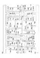
図3は、図2に示した上記回路ブロック1のレイアウト例を示すものである。本実施形態の場合、たとえばp型半導体基板31の表面部には、上記p型MOSFET12a,12b,13a,13bのソース/ドレイン拡散層(ソース/ドレイン電極)となるp型拡散領域32a,33a,34a,35a,36aと、上記p型MOSFET11a,14aのソース/ドレイン拡散層となるp型拡散領域37a,38a,39aとが形成されている。また、上記p型半導体基板31の他の表面部には、上記n型MOSFET12c,12d,13c,13dのソース/ドレイン拡散層となるn型拡散領域42a,43a,44a,45a,46aと、上記n型MOSFET11b,14bのソース/ドレイン拡散層となるn型拡散領域47a,48a,49aとが形成されている。  FIG. 3 shows a layout example of thecircuit block 1 shown in FIG. In the case of the present embodiment, for example, on the surface portion of the p-type semiconductor substrate 31, the p-type diffusion regions 32a, 33a, which become the source / drain diffusion layers (source / drain electrodes) of the p-type MOSFETs 12a, 12b, 13a, 13b. 34a, 35a, and 36a, and p-type diffusion regions 37a, 38a, and 39a that serve as source / drain diffusion layers of the p-type MOSFETs 11a and 14a are formed. Further, on the other surface portion of the p-type semiconductor substrate 31, n-type diffusion regions 42a, 43a, 44a, 45a, 46a that become source / drain diffusion layers of the n-type MOSFETs 12c, 12d, 13c, 13d, and the above-mentioned N-type diffusion regions 47a, 48a, and 49a are formed as source / drain diffusion layers of the n-type MOSFETs 11b and 14b.

また、上記p型拡散領域32a,33a間の上方には、図示していないゲート絶縁膜を介して、上記p型MOSFET13aのゲート電極13a−Gが設けられている。同様に、上記p型拡散領域33a,34a間の上方には、図示していないゲート絶縁膜を介して、上記p型MOSFET13bのゲート電極13b−Gが設けられている。同様に、上記p型拡散領域34a,35a間の上方には、図示していないゲート絶縁膜を介して、上記p型MOSFET12bのゲート電極12b−Gが設けられている。同様に、上記p型拡散領域35a,36a間の上方には、図示していないゲート絶縁膜を介して、上記p型MOSFET12aのゲート電極12a−Gが設けられている。  Agate electrode 13a-G of the p-type MOSFET 13a is provided above the p-type diffusion regions 32a and 33a through a gate insulating film (not shown). Similarly, agate electrode 13b-G of the p-type MOSFET 13b is provided above the p-type diffusion regions 33a and 34a via a gate insulating film (not shown). Similarly, agate electrode 12b-G of the p-type MOSFET 12b is provided above the p-type diffusion regions 34a and 35a via a gate insulating film (not shown). Similarly, agate electrode 12a-G of the p-type MOSFET 12a is provided above the p-type diffusion regions 35a and 36a via a gate insulating film (not shown).

さらに、上記p型拡散領域37a,38a間の上方には、図示していないゲート絶縁膜を介して、上記p型MOSFET11aのゲート電極11a−Gが設けられている。同様に、上記p型拡散領域38a,39a間の上方には、図示していないゲート絶縁膜を介して、上記p型MOSFET14aのゲート電極14a−Gが設けられている。  Further, agate electrode 11a-G of the p-type MOSFET 11a is provided above the p-type diffusion regions 37a and 38a via a gate insulating film (not shown). Similarly, agate electrode 14a-G of the p-type MOSFET 14a is provided above the p-type diffusion regions 38a and 39a via a gate insulating film (not shown).

一方、上記n型拡散領域42a,43a間の上方には、図示していないゲート絶縁膜を介して、上記n型MOSFET13dのゲート電極13d−Gが設けられている。同様に、上記n型拡散領域43a,44a間の上方には、図示していないゲート絶縁膜を介して、上記n型MOSFET13cのゲート電極13c−Gが設けられている。同様に、上記n型拡散領域44a,45a間の上方には、図示していないゲート絶縁膜を介して、上記n型MOSFET12cのゲート電極12c−Gが設けられている。同様に、上記n型拡散領域45a,46a間の上方には、図示していないゲート絶縁膜を介して、上記n型MOSFET12dのゲート電極12d−Gが設けられている。  On the other hand, agate electrode 13d-G of the n-type MOSFET 13d is provided above the n-type diffusion regions 42a and 43a via a gate insulating film (not shown). Similarly, agate electrode 13c-G of the n-type MOSFET 13c is provided above the n-type diffusion regions 43a and 44a via a gate insulating film (not shown). Similarly, agate electrode 12c-G of the n-type MOSFET 12c is provided above the n-type diffusion regions 44a and 45a via a gate insulating film (not shown). Similarly, thegate electrode 12d-G of the n-type MOSFET 12d is provided above the n-type diffusion regions 45a and 46a via a gate insulating film (not shown).

さらに、上記n型拡散領域47a,48a間の上方には、図示していないゲート絶縁膜を介して、上記n型MOSFET11bのゲート電極11b−Gが設けられている。同様に、上記n型拡散領域48a,49a間の上方には、図示していないゲート絶縁膜を介して、上記n型MOSFET14bのゲート電極14b−Gが設けられている。  Further, agate electrode 11b-G of the n-type MOSFET 11b is provided above the n-type diffusion regions 47a and 48a via a gate insulating film (not shown). Similarly, agate electrode 14b-G of the n-type MOSFET 14b is provided above the n-type diffusion regions 48a and 49a via a gate insulating film (not shown).

上記ゲート電極13a−Gおよび上記ゲート電極13d−Gは、配線コンタクト51aおよび第1層配線52aを介して、上記端子Dに接続されている。また、上記ゲート電極13b−Gおよび上記ゲート電極12c−Gは、配線コンタクト51bを介して、上記クロック信号CKを供給するための第2層配線53aに接続されている。また、上記ゲート電極12b−Gおよび上記ゲート電極13c−Gは、配線コンタクト51c,51dを介して、上記反転クロック信号CKBを供給するための第2層配線53bに接続されている。また、上記ゲート電極12a−Gおよび上記ゲート電極12d−Gは、配線コンタクト51e、第1層配線52b、および、配線コンタクト51fを介して、上記ゲート電極14a−Gおよび上記ゲート電極14b−Gに接続されている。さらに、上記ゲート電極12a−Gおよび上記ゲート電極12d−Gにつながる上記第1層配線52bは、拡散層コンタクト54a,54bを介して、上記p型拡散領域37aおよび上記n型拡散領域47aに接続されている。また、上記ゲート電極11a−Gおよび上記ゲート電極11b−Gは、配線コンタクト51g、第1層配線52c、および、拡散層コンタクト54c,54dを介して、上記p型拡散領域34aおよび上記n型拡散領域44aに接続されている。  Thegate electrode 13a-G and thegate electrode 13d-G are connected to the terminal D through awiring contact 51a and afirst layer wiring 52a. Thegate electrode 13b-G and thegate electrode 12c-G are connected to asecond layer wiring 53a for supplying the clock signal CK through awiring contact 51b. Thegate electrode 12b-G and thegate electrode 13c-G are connected to asecond layer wiring 53b for supplying the inverted clock signal CKB throughwiring contacts 51c and 51d. Thegate electrode 12a-G and thegate electrode 12d-G are connected to thegate electrode 14a-G and thegate electrode 14b-G via thewiring contact 51e, thefirst layer wiring 52b, and thewiring contact 51f. It is connected. Further, thefirst layer wiring 52b connected to thegate electrode 12a-G and thegate electrode 12d-G is connected to the p-type diffusion region 37a and the n-type diffusion region 47a viadiffusion layer contacts 54a and 54b. Has been. Thegate electrode 11a-G and thegate electrode 11b-G are connected to the p-type diffusion region 34a and the n-type diffusion via thewiring contact 51g, thefirst layer wiring 52c, and thediffusion layer contacts 54c and 54d. It is connected to theregion 44a.

上記p型拡散領域32a,36a,38aには、拡散層コンタクト54e,54f,54gを介して、上記電源電位VDDを供給するための第1層配線52dが接続されている。また、上記n型拡散領域42a,46a,48aには、拡散層コンタクト54h,54i,54jを介して、上記接地電位VSSを供給するための第1層配線52eが接続されている。さらに、上記p型拡散領域39aおよび上記n型拡散領域49aは、拡散層コンタクト54k,54mおよび第1層配線52fを介して、上記回路ブロック2の上記クロックドインバータ23の入力端に接続されている。  Afirst layer wiring 52d for supplying the power supply potential VDD is connected to the p-type diffusion regions 32a, 36a, and 38a throughdiffusion layer contacts 54e, 54f, and 54g. Afirst layer wiring 52e for supplying the ground potential VSS is connected to the n-type diffusion regions 42a, 46a, and 48a viadiffusion layer contacts 54h, 54i, and 54j. Further, the p-type diffusion region 39a and the n-type diffusion region 49a are connected to the input terminal of the clockedinverter 23 of the circuit block 2 via thediffusion layer contacts 54k and 54m and thefirst layer wiring 52f. Yes.

なお、本実施形態の場合、上記n型MOSFET12cと上記n型MOSFET12dとのゲート電極12c−G,12d−G間の距離Xが、その他の、たとえば上記n型MOSFET13cと上記n型MOSFET13dとのゲート電極13c−G,13d−G間の距離Yなどよりも小さくなるように設計されている(X<Y)。  In the case of this embodiment, the distance X between thegate electrodes 12c-G and 12d-G between the n-type MOSFET 12c and the n-type MOSFET 12d is the other, for example, the gate between the n-type MOSFET 13c and the n-type MOSFET 13d. It is designed to be smaller than the distance Y between theelectrodes 13c-G and 13d-G (X <Y).

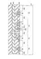
図4は、図3のIV−IV線に沿う部位の断面構造をより詳細に示すものである。すなわち、上記p型半導体基板31の表面上には、上記ゲート電極13d−G,13c−G,12c−G,12d−Gが、それぞれ設けられている。上記ゲート電極13d−G,13c−G,12c−G,12d−Gの両サイドには、それぞれ、側壁絶縁膜(サイドウォール)57が形成されている。上記側壁絶縁膜57にそれぞれ対応する、上記p型半導体基板31の表面部には、接合の浅い、たとえば30nm程度の接合深さを有するエクステンション領域(第2の拡散領域)58が形成されている。また、上記n型MOSFET12cと上記n型MOSFET12dとの間を除く、上記p型半導体基板31の表面部には、それぞれ、上記エクステンション領域58よりも接合の深い、たとえば150nm〜200nm程度の接合深さを有する、上記n型拡散領域(第1の拡散領域)42a,43a,44a,46aが形成されている。  FIG. 4 shows in more detail the cross-sectional structure of the site along line IV-IV in FIG. That is, thegate electrodes 13d-G, 13c-G, 12c-G, and 12d-G are provided on the surface of the p-type semiconductor substrate 31, respectively. Side wall insulating films (sidewalls) 57 are formed on both sides of thegate electrodes 13d-G, 13c-G, 12c-G, and 12d-G, respectively. An extension region (second diffusion region) 58 having a shallow junction, for example, a junction depth of about 30 nm, is formed on the surface portion of the p-type semiconductor substrate 31 corresponding to each of thesidewall insulating films 57. . Moreover, the junction depth deeper than theextension region 58, for example, about 150 nm to 200 nm, is formed on the surface portion of the p-type semiconductor substrate 31 except between the n-type MOSFET 12c and the n-type MOSFET 12d. The n-type diffusion regions (first diffusion regions) 42a, 43a, 44a, 46a are formed.

これに対し、上記n型MOSFET12cと上記n型MOSFET12dとの間に対応する、上記p型半導体基板31の表面部には、上記エクステンション領域58のみからなる上記n型拡散領域(第2の拡散層)45aが形成されている。すなわち、上記n型MOSFET13c,13dは、それぞれ、上記エクステンション領域58と上記n型拡散領域42a,43a,44aとからなるソース/ドレイン拡散層を有して構成されている。一方、上記n型MOSFET12cは、ソース/ドレイン拡散層のいずれか一方(この場合、ソース拡散層)が、上記エクステンション領域58からなる上記n型拡散領域45aのみの第2の拡散層により構成され、ソース/ドレイン拡散層のいずれか他方(この場合、ドレイン拡散層)が、上記エクステンション領域58と上記n型拡散領域44aとからなる第1の拡散層により構成されている。同様に、上記n型MOSFET12dは、ソース/ドレイン拡散層のいずれか一方(この場合、ドレイン拡散層)が、上記エクステンション領域58からなる上記n型拡散領域45aのみの第2の拡散層により構成され、ソース/ドレイン拡散層のいずれか他方(この場合、ソース拡散層)が、上記エクステンション領域58と上記n型拡散領域46aとからなる第1の拡散層により構成されている。  On the other hand, on the surface portion of the p-type semiconductor substrate 31 corresponding to the space between the n-type MOSFET 12c and the n-type MOSFET 12d, the n-type diffusion region (second diffusion layer) consisting only of theextension region 58 is provided. ) 45a is formed. That is, the n-type MOSFETs 13c and 13d are each configured to have a source / drain diffusion layer composed of theextension region 58 and the n-type diffusion regions 42a, 43a and 44a. On the other hand, in the n-type MOSFET 12c, either one of the source / drain diffusion layers (in this case, the source diffusion layer) is configured by a second diffusion layer including only the n-type diffusion region 45a including theextension region 58, The other of the source / drain diffusion layers (in this case, the drain diffusion layer) is constituted by a first diffusion layer composed of theextension region 58 and the n-type diffusion region 44a. Similarly, in the n-type MOSFET 12d, either one of the source / drain diffusion layers (in this case, the drain diffusion layer) is configured by a second diffusion layer including only the n-type diffusion region 45a including theextension region 58. The other of the source / drain diffusion layers (in this case, the source diffusion layer) is constituted by a first diffusion layer composed of theextension region 58 and the n-type diffusion region 46a.

本実施形態の場合、上記ゲート電極12c−G,12d−G間の距離(ゲート間ピッチ)Xを、たとえば0.1μm〜0.2μm程度とすることにより、上記n型MOSFET12cと上記n型MOSFET12dとの間の、上記p型半導体基板31の表面部に、接合深さが浅い第2の拡散領域のみからなる第2の拡散層が形成されるようになっている。つまり、上記n型MOSFET12cと上記n型MOSFET12dとのゲート電極12c−G,12d−G間の距離Xを、双方の側壁絶縁膜57が接するように狭く形成する。こうすることによって、上記n型MOSFET12cと上記n型MOSFET12dとの間の、上記p型半導体基板31の表面部に接合深さが深い第1の拡散領域が形成されるのを阻止できる。  In the case of this embodiment, the distance (gate pitch) X between thegate electrodes 12c-G, 12d-G is set to, for example, about 0.1 μm to 0.2 μm, so that the n-type MOSFET 12c and the n-type MOSFET 12d. A second diffusion layer consisting only of the second diffusion region having a shallow junction depth is formed on the surface portion of the p-type semiconductor substrate 31 between the first and second layers. That is, the distance X between thegate electrodes 12c-G and 12d-G between the n-type MOSFET 12c and the n-type MOSFET 12d is narrowly formed so that both sidewall insulatingfilms 57 are in contact with each other. By doing so, it is possible to prevent the first diffusion region having a deep junction depth from being formed on the surface portion of the p-type semiconductor substrate 31 between the n-type MOSFET 12c and the n-type MOSFET 12d.

なお、上記p型半導体基板31の表面上には、層間絶縁膜59a,59b,59cが積層されている。上記層間絶縁膜59aには、上記n型拡散領域44aにつながる上記拡散層コンタクト54dが形成されている。上記層間絶縁膜59bには、上記拡散層コンタクト54dにつながる上記第1層配線52cが形成されている。  On the surface of the p-type semiconductor substrate 31,interlayer insulating films 59a, 59b and 59c are stacked. In theinterlayer insulating film 59a, thediffusion layer contact 54d connected to the n-type diffusion region 44a is formed. In theinterlayer insulating film 59b, thefirst layer wiring 52c connected to thediffusion layer contact 54d is formed.

次に、このような断面構造を有するn型MOSFETを形成するためのプロセスについて説明する。素子分離、ゲート酸化膜およびゲート電極の形成には、広く知られている技術(Sze.:VLSI Technology,Mcgrowhill)を用いることができる。すなわち、上記ゲート電極12c−G,12d−G,13c−G,13d−Gの形成後、イオン注入技術を用いて、上記p型半導体基板31の表面部にn型不純物を導入し、上記エクステンション領域58を形成する。次いで、シリコン窒化膜もしくはシリコン酸化膜をChemical Vapor Deposition(CVD)法により堆積し、その後、上記シリコン窒化膜もしくは上記シリコン酸化膜をエッチングして、上記ゲート電極12c−G,12d−G,13c−G,13d−Gの各側面に、上記側壁絶縁膜57,57を形成する。この側壁絶縁膜57,57の横方向の厚みは、堆積したシリコン窒化膜もしくはシリコン酸化膜の膜厚により制御できる。  Next, a process for forming an n-type MOSFET having such a cross-sectional structure will be described. A widely known technique (Sze .: VLSI Technology, Mcgrowhill) can be used for element isolation, gate oxide film formation, and gate electrode formation. That is, after forming thegate electrodes 12c-G, 12d-G, 13c-G, and 13d-G, an n-type impurity is introduced into the surface portion of the p-type semiconductor substrate 31 by using an ion implantation technique, and theextension Region 58 is formed. Next, a silicon nitride film or a silicon oxide film is deposited by a chemical vapor deposition (CVD) method, and then the silicon nitride film or the silicon oxide film is etched to form thegate electrodes 12c-G, 12d-G, 13c- Thesidewall insulating films 57 and 57 are formed on the side surfaces of G and 13d-G. The lateral thickness of thesidewall insulating films 57, 57 can be controlled by the thickness of the deposited silicon nitride film or silicon oxide film.

本実施形態では、シリコン窒化膜もしくはシリコン酸化膜を、少なくとも上記n型MOSFET12cおよび上記n型MOSFET12dのゲート電極12c−G,12d−G間の距離X(=0.1μm〜0.2μm)よりも厚く堆積する。これにより、図4に示したように、2つのゲート電極12c−G,12d−Gの側壁絶縁膜57,57が接した状態になる。この状態で、上記n型拡散領域42a,43a,44a,46a(47a,48a,49a)を形成するための、n型不純物をイオン注入する。すると、上記ゲート電極12c−G,12d−G間においては、接した側壁絶縁膜57,57がブロックとなり、その下の上記p型半導体基板31の表面部には、接合深さが浅い、上記エクステンション領域58のみからなる上記n型拡散領域45a以外の、接合深さが深いn型拡散領域は形成されない。  In the present embodiment, the silicon nitride film or the silicon oxide film is at least more than the distance X (= 0.1 μm to 0.2 μm) between thegate electrodes 12c-G and 12d-G of the n-type MOSFET 12c and the n-type MOSFET 12d. Deposits thick. As a result, as shown in FIG. 4, the sidewall insulating films 57 and 57 of the twogate electrodes 12c-G and 12d-G are brought into contact with each other. In this state, n-type impurities are ion-implanted to form the n-type diffusion regions 42a, 43a, 44a, 46a (47a, 48a, 49a). Then, between thegate electrodes 12c-G and 12d-G, the sidewall insulating films 57 and 57 in contact with each other become a block, and the junction portion has a shallow junction depth on the surface portion of the p-type semiconductor substrate 31 below. An n-type diffusion region having a deep junction depth other than the n-type diffusion region 45a composed only of theextension region 58 is not formed.

ここで、たとえばノード60aの電位が“H”のとき、上記n型MOSFET12cのドレイン拡散層(上記n型拡散領域44aおよび上記エクステンション領域58)と上記p型半導体基板31との間のPN接合は逆バイアスになる。このドレイン拡散層にα線が入射すると、上記p型半導体基板31中で生成したキャリアのうちの電子(電荷)が、上記ドレイン拡散層に収集される。収集された電荷は、上記ノード60aの電位を下げる。この電位が、上記インバータ回路11の回路しきい値を下回ると、ノード60bの電位が“L”から“H”へと変化する。その結果、このラッチ回路10の情報が、もともともっていた情報と反対の情報に書き換えられる。これが、ソフトエラーと呼ばれる現象である。上記ドレイン拡散層が深い接合の場合、そのドレイン拡散層に収集される電荷量が甚大となり、ソフトエラーが頻発する。この現象は、上記ラッチ回路10の、n型およびp型のすべての拡散層(p型拡散領域34a,35a,37aおよびn型拡散領域44a,45a,47a)で起こり得る。なお、ソフトエラーが起こるかどうかは、α線の入射条件、ウェルの形成条件、電源電圧、上記ノード60a,60bの容量、および、上記インバータ回路11と上記クロックドインバータ12との反応時間などに応じて異なる。  For example, when the potential of thenode 60a is “H”, the PN junction between the drain diffusion layer (the n-type diffusion region 44a and the extension region 58) of the n-type MOSFET 12c and the p-type semiconductor substrate 31 is Reverse bias. When α rays are incident on the drain diffusion layer, electrons (charges) of carriers generated in the p-type semiconductor substrate 31 are collected in the drain diffusion layer. The collected charge lowers the potential of thenode 60a. When this potential falls below the circuit threshold value of theinverter circuit 11, the potential of thenode 60b changes from “L” to “H”. As a result, the information in thelatch circuit 10 is rewritten to the opposite information from the original information. This is a phenomenon called soft error. When the drain diffusion layer has a deep junction, the amount of charge collected in the drain diffusion layer becomes large, and soft errors frequently occur. This phenomenon can occur in all of the n-type and p-type diffusion layers (p-type diffusion regions 34a, 35a, 37a and n-type diffusion regions 44a, 45a, 47a) of thelatch circuit 10. Whether a soft error occurs depends on the incident condition of α rays, the conditions for forming wells, the power supply voltage, the capacitance of thenodes 60a and 60b, the reaction time between theinverter circuit 11 and the clockedinverter 12, and the like. Depending on.

上記した回路構成を有するDelay型のフリップ・フロップの場合、特に、上記クロックドインバータ12を構成する、上記n型MOSFET12cのソース/ドレイン拡散層(上記n型拡散領域44a,45a)が、ソフトエラーに弱い。そこで、本実施形態では、短チャンネル効果抑制のための浅い接合(エクステンション領域58)と寄生抵抗を低減させるための深い接合(n型拡散領域42a,43a,44a,46a,47a,48a,49a)とを組み合わせて形成されているソース/ドレイン拡散層のうち、少なくともソフトエラーに弱い部位のドレイン拡散層(n型拡散領域45a)を、浅い接合(エクステンション領域58)のみで形成する。  In the case of the delay flip-flop having the circuit configuration described above, in particular, the source / drain diffusion layers (the n-type diffusion regions 44a and 45a) of the n-type MOSFET 12c constituting the clockedinverter 12 are soft errors. Vulnerable to Therefore, in this embodiment, a shallow junction (extension region 58) for suppressing the short channel effect and a deep junction (n-type diffusion regions 42a, 43a, 44a, 46a, 47a, 48a, 49a) for reducing parasitic resistance. Among the source / drain diffusion layers formed in combination, at least a drain diffusion layer (n-type diffusion region 45a) that is vulnerable to a soft error is formed only by a shallow junction (extension region 58).

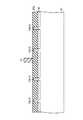
以下に、n型MOSFET12cのドレイン拡散層を浅い接合のみによって形成した場合の効果(ソフトエラーに与える影響)について説明する。図5は、上記p型半導体基板31を深さ方向に切断した場合の不純物の分布を示すものである。図5中の61は、たとえば図4のVa−Va線に沿う断面での不純物の分布であり、62は、たとえば図4のVb−Vb線に沿う断面での不純物の分布である。  Hereinafter, an effect (influence on a soft error) when the drain diffusion layer of the n-type MOSFET 12c is formed only by a shallow junction will be described. FIG. 5 shows the distribution of impurities when the p-type semiconductor substrate 31 is cut in the depth direction. In FIG. 5, for example, 61 is an impurity distribution in a cross section along the line Va-Va in FIG. 4, and 62 is an impurity distribution in a cross section along the line Vb-Vb in FIG. 4, for example.

図5に示すように、上記p型半導体基板31のp型不純物の分布63は、しきい値制御のため、基板表面に向かって濃度が高くなっている。つまり、このp型不純物の分布63は、深い接合の拡散層(上記n型拡散領域44a)を形成するn型不純物の分布61と交差する濃度に対し、浅い接合の拡散層(上記n型拡散領域45a)を形成するn型不純物の分布62と交差する濃度が1桁程度高くなっている。Hu氏の電荷収集モデル(たとえば、IEEE EDL Vol EDL−3,No.2,Feb 1982)によると、収集電荷は空乏層の幅に比例する。よって、空乏層の幅が狭い、浅い接合の拡散層の方が収集電荷量は小さくなり、ソフトエラーに強くなる。  As shown in FIG. 5, the p-type impurity distribution 63 of the p-type semiconductor substrate 31 has a higher concentration toward the substrate surface for threshold control. That is, the p-type impurity distribution 63 is shallower than the n-type impurity distribution 61 forming the deep junction diffusion layer (the n-type diffusion region 44a). The concentration intersecting with the n-type impurity distribution 62 forming theregion 45a) is about one digit higher. According to Hu's charge collection model (eg, IEEE EDL Vol EDL-3, No. 2, Feb 1982), the collected charge is proportional to the width of the depletion layer. Therefore, the shallow junction diffusion layer having a narrow depletion layer has a smaller amount of collected charge and is more resistant to soft errors.

また、たとえば図6に示すように、深い接合の拡散層64よりも浅い接合の拡散層65の方が、斜めに入射するα線(α粒子)に対しては当たり難くなる効果も期待できる。  Further, for example, as shown in FIG. 6, it can be expected that thediffusion layer 65 having a shallow junction than thediffusion layer 64 having a deep junction is less likely to hit α rays (α particles) incident obliquely.

シミュレーションによると、これらの効果により、従来よりもソフトエラーレートを65%ほど減少させることが可能となる。  According to the simulation, it is possible to reduce the soft error rate by about 65% as compared with the conventional technique due to these effects.

上記したように、ロジック回路を構成するMOSFETの拡散層での収集電荷量を減少できるようにしている。すなわち、宇宙線やα線によって生成されるキャリアのうちの電荷を収集する拡散層を、30nm程度の浅い接合により形成するようにしている。これにより、その拡散層での収集電荷量を減らすことが可能となる結果、それに起因して発生する電気的ノイズを弱くできる。したがって、拡散層が回路ノードとして保持していた情報を書き換えしまうといった、ECCなどでの救済が困難なロジック回路(フリップ・フロップ)のソフトエラー耐性を簡単に向上できるようになるものである。  As described above, the amount of collected charges in the diffusion layer of the MOSFET constituting the logic circuit can be reduced. In other words, the diffusion layer that collects the charge of carriers generated by cosmic rays and α rays is formed by a shallow junction of about 30 nm. As a result, the amount of collected charges in the diffusion layer can be reduced. As a result, electrical noise generated due to the amount can be reduced. Therefore, it is possible to easily improve the soft error resistance of a logic circuit (flip-flop) that is difficult to relieve by ECC, such as rewriting information held in the diffusion layer as a circuit node.

しかも、LDD(Lightly Doped Drain)構造を利用するようにしているため、浅い接合の拡散層は、ゲート電極のレイアウトの一部を変更することのみによって自動的に形成することが可能である。つまり、回路設計や形成プロセスの複雑化を招いたりすることなく、容易に実現し得るものである。  In addition, since the LDD (Lightly Doped Drain) structure is used, the shallow junction diffusion layer can be automatically formed only by changing a part of the layout of the gate electrode. That is, it can be easily realized without complicating circuit design or formation process.

特に、接合の浅い、n型拡散領域45aの寄生抵抗成分は、ゲート電極12c−G,12d−G間の距離Xを小さくすることで、接合の深い、n型拡散領域42a,43a,44a,46aよりも高くなるのを解消できる。  Particularly, the parasitic resistance component of the n-type diffusion region 45a having a shallow junction can be obtained by reducing the distance X between thegate electrodes 12c-G and 12d-G, thereby reducing the n-type diffusion regions 42a, 43a, 44a, and It can be eliminated that the height is higher than 46a.

なお、上記した第1の実施形態においては、ゲート電極12c−G,12d−G間の距離Xを小さくすることによって(X<Y)、上記n型MOSFET12cと上記n型MOSFET12dとの間の、上記p型半導体基板31の表面部に、浅い接合の拡散層(n型拡散領域45a)を形成するようにした場合について説明した。これに限らず、たとえば図7および図8に示すように、浅い接合の拡散層(n型拡散領域45a)としては、ゲート電極12c−G,12d−G間の距離Xを小さくすることなしに形成することも可能である(X=Y)。  In the first embodiment described above, by reducing the distance X between thegate electrodes 12c-G and 12d-G (X <Y), the n-type MOSFET 12c and the n-type MOSFET 12d are The case where a shallow junction diffusion layer (n-type diffusion region 45a) is formed on the surface portion of the p-type semiconductor substrate 31 has been described. For example, as shown in FIGS. 7 and 8, the shallow junction diffusion layer (n-type diffusion region 45a) can be used without reducing the distance X between thegate electrodes 12c-G and 12d-G. It is also possible to form (X = Y).

つまり、上記n型MOSFET12c,12d,13c,13dの各ゲート電極12c−G,12d−G,13c−G,13d−G間の距離は、等間隔とする。そして、上記n型MOSFET12cと上記n型MOSFET12dとの間の、上記p型半導体基板31の表面部には、上記エクステンション領域58と同じ接合深さを有する、接合の浅い上記n型拡散領域45aのみを形成する。一方、上記n型MOSFET12cと上記n型MOSFET12dとの間を除く、上記p型半導体基板31の表面部には、それぞれ、上記n型拡散領域45aよりも接合の深い上記n型拡散領域42a,43a,44a,46aを形成する。この場合、接合の浅い上記n型拡散領域45aは、接合の深い上記n型拡散領域42a,43a,44a,46aの形成を行うことなく、上記エクステンション領域58をそのまま残存させることによって簡単に形成できる。  That is, the distances between thegate electrodes 12c-G, 12d-G, 13c-G, and 13d-G of the n-type MOSFETs 12c, 12d, 13c, and 13d are equal. Only the shallow junction n-type diffusion region 45a having the same junction depth as theextension region 58 is provided on the surface portion of the p-type semiconductor substrate 31 between the n-type MOSFET 12c and the n-type MOSFET 12d. Form. On the other hand, on the surface portion of the p-type semiconductor substrate 31 except between the n-type MOSFET 12c and the n-type MOSFET 12d, the n-type diffusion regions 42a and 43a having a junction deeper than the n-type diffusion region 45a, respectively. , 44a, 46a. In this case, the n-type diffusion region 45a having a shallow junction can be easily formed by leaving theextension region 58 as it is without forming the n-type diffusion regions 42a, 43a, 44a and 46a having a deep junction. .

[第2の実施形態]
図9〜図11は、この発明の第2の実施形態にしたがったロジック回路の基本構成を示すものである。ここでは、図2に示したDelay型フリップ・フロップの回路ブロック1において、n型MOSFET12cのゲート電極12c−Gと拡散層コンタクト54dとの間に、部分的に、エクステンション領域58と同じ接合深さを有する、接合の浅いn型拡散領域を形成するようにした場合について説明する。なお、図9は回路ブロックの具体的構成を示す回路図であり、図10は図9に示した回路ブロックのレイアウト図であり、図11は図10のXI−XI線に沿う部位の断面構造を示す図である。
[Second Embodiment]
9 to 11 show a basic configuration of a logic circuit according to the second embodiment of the present invention. Here, in thecircuit block 1 of the Delay-type flip-flop shown in FIG. 2, the junction depth is partially the same as that of theextension region 58 between thegate electrode 12c-G of the n-type MOSFET 12c and thediffusion layer contact 54d. A case where an n-type diffusion region having a shallow junction is formed will be described. 9 is a circuit diagram showing a specific configuration of the circuit block, FIG. 10 is a layout diagram of the circuit block shown in FIG. 9, and FIG. 11 is a sectional structure of a portion along the line XI-XI in FIG. FIG.

すなわち、本実施形態の場合、回路ブロック1’のラッチ回路10’を構成するクロックドインバータ12Aの、上記n型MOSFET12cのドレイン拡散層(ドレイン電極)が、チャネルに隣接するエクステンション領域(第2の拡散領域)58と、接合の深いn型拡散領域(第1の拡散領域)44a-1と、上記チャネルに隣接しない接合の浅いn型拡散領域(第3の拡散領域)70と、接合の深いn型拡散領域(第4の拡散領域)44a-2とから構成されている。That is, in this embodiment, the drain diffusion layer (drain electrode) of the n-type MOSFET 12c of the clockedinverter 12A constituting thelatch circuit 10 ′ of thecircuit block 1 ′ is an extension region (second region) adjacent to the channel. A diffusion region) 58, a deep junction n-type diffusion region (first diffusion region) 44a-1 , a junction shallow n-type diffusion region (third diffusion region) 70 not adjacent to the channel, and a deep junction. and an n-type diffusion region (fourth diffusion region) 44a-2 .

このような構成のドレイン拡散層を形成する場合、まずは、たとえば図12に示すように、ゲート電極12c−G,12d−G,13c−G,13d−Gを形成する。その際、上記ゲート電極12c−G,13c−G間の距離Zが、その他の、たとえば上記ゲート電極12c−G,12d−G間の距離Xおよび上記ゲート電極13c−G,13d−G間の距離Yなどよりも大きくなるようにする(Z>X,Y)。この後、p型半導体基板31の表面部に、接合の浅い上記エクステンション領域58を形成する。次いで、シリコン窒化膜もしくはシリコン酸化膜などの絶縁膜57aを、CVD法により堆積する。その後、レジストをパターニングして、レジストパターン72を形成する。そして、このレジストパターン72をマスクに上記絶縁膜57aをエッチングすることによって、側壁絶縁膜57,57を形成すると同時に、接合の深いn型拡散領域の形成を部分的に阻止するための絶縁膜パターン57’を形成する(図11参照)。今度は、上記絶縁膜パターン57’および上記側壁絶縁膜57,57をマスクに、接合の深いn型拡散領域42a,43a,44a-1,44a-2,45a,46a(47a,48a,49a)を形成するための、n型不純物をイオン注入する。すると、上記ゲート電極12c−G,12d−G間の、上記p型半導体基板31の表面部には、接合深さが浅い、上記エクステンション領域(第2の拡散領域)58と、接合深さが深い、上記n型拡散領域(第1の拡散領域)45aとからなるソース拡散層(第1の拡散層)が形成される。When forming the drain diffusion layer having such a configuration, first, as shown in FIG. 12, for example,gate electrodes 12c-G, 12d-G, 13c-G, and 13d-G are formed. At this time, the distance Z between thegate electrodes 12c-G and 13c-G is equal to other distance X between thegate electrodes 12c-G and 12d-G and the distance between thegate electrodes 13c-G and 13d-G. The distance Y is made larger than Z (X> X, Y). Thereafter, theextension region 58 having a shallow junction is formed on the surface portion of the p-type semiconductor substrate 31. Next, an insulatingfilm 57a such as a silicon nitride film or a silicon oxide film is deposited by a CVD method. Thereafter, the resist is patterned to form a resistpattern 72. Then, by etching the insulatingfilm 57a using the resistpattern 72 as a mask, the sidewall insulating films 57 and 57 are formed, and at the same time, an insulating film pattern for partially preventing the formation of a deep junction n-type diffusion region 57 'is formed (see FIG. 11). This time, with the insulating film pattern 57 'and the sidewall insulating films 57, 57 as masks, deep junction n-type diffusion regions 42a, 43a, 44a-1 , 44a-2 , 45a, 46a (47a, 48a, 49a). An n-type impurity is ion-implanted to form n. Then, the junction depth is shallow at the surface portion of the p-type semiconductor substrate 31 between thegate electrodes 12c-G and 12d-G, the extension region (second diffusion region) 58, and the junction depth are A deep source diffusion layer (first diffusion layer) composed of the n-type diffusion region (first diffusion region) 45a is formed.

一方、上記ゲート電極12c−G,13c−G間では、上記側壁絶縁膜57,57および上記絶縁膜パターン57’がブロックとなり、その下の上記p型半導体基板31の表面部には、接合深さが浅い、上記エクステンション領域58および上記エクステンション領域58のみからなる上記n型拡散領域70以外の、接合深さが深いn型拡散領域は形成されない。これにより、上記ゲート電極12c−G,13c−G間においては、接合の深い上記n型拡散領域44a-1,44a-2の相互間に接合の浅い上記n型拡散領域70が選択的に設けられてなるドレイン拡散層(第2の拡散層)が形成される。On the other hand, between thegate electrodes 12c-G and 13c-G, the sidewall insulating films 57 and 57 and the insulatingfilm pattern 57 ′ become a block, and the surface portion of the p-type semiconductor substrate 31 therebelow has a junction depth. An n-type diffusion region having a deep junction depth other than the n-type diffusion region 70 composed of only theextension region 58 and theextension region 58 is not formed. Thereby, between thegate electrodes 12c-G and 13c-G, the shallow n-type diffusion region 70 is selectively provided between the deep n-type diffusion regions 44a-1 and 44a-2. Thus formed drain diffusion layer (second diffusion layer) is formed.

本実施形態の場合、上述した第1の実施形態の場合と同様に、接合の浅いn型拡散領域70は、α線の入射に対して、収集電荷量を減少させる効果がある。また、接合の浅いn型拡散領域70は、その寄生抵抗成分が、接合の深いn型拡散領域44a-1,44a-2よりも高くなる。これにより、α線によって生成される電荷が上記n型拡散領域45aで収集される場合にも、電荷の収集によるノイズ(電位変動)がノード60aに伝達されるのを妨げることが可能となる。したがって、上記ラッチ回路10’が保持している情報を書き換えにくくなる結果、ソフトエラーレートの低減に有効である。In the case of the present embodiment, as in the case of the first embodiment described above, the shallow junction n-type diffusion region 70 has the effect of reducing the collected charge amount with respect to the incidence of α rays. In addition, the shallow junction n-type diffusion region 70 has a higher parasitic resistance component than the deep junction n-type diffusion regions 44a-1 and 44a-2 . Thereby, even when charges generated by α rays are collected by the n-type diffusion region 45a, it is possible to prevent noise (potential fluctuation) due to charge collection from being transmitted to thenode 60a. Therefore, it becomes difficult to rewrite the information held by the latch circuit 10 ', and this is effective in reducing the soft error rate.

なお、本実施形態においては、たとえば図13に示すように、上記n型MOSFET12cのゲート電極12c−Gの側壁絶縁膜57,57の一方(ドレイン電極側)と連続するように、上記絶縁膜パターン57’を配置してもよい。この場合、上記ゲート電極12c−G,13c−G間においては、チャネルに隣接するエクステンション領域(第2の拡散領域)58と、接合の深いn型拡散領域(第1の拡散領域)44aとからなるドレイン拡散層(第2の拡散層)が形成される。すなわち、上記n型MOSFET12cにおいて、上記チャネルの端部から上記n型拡散領域44a,45aまでの距離が、ソース拡散層よりもドレイン拡散層の方が長くなるように形成した場合にも上記と同様の効果が期待できる。  In the present embodiment, for example, as shown in FIG. 13, the insulating film pattern is continuous with one of the sidewall insulating films 57 and 57 (on the drain electrode side) of thegate electrode 12c-G of the n-type MOSFET 12c. 57 'may be arranged. In this case, between thegate electrodes 12c-G and 13c-G, the extension region (second diffusion region) 58 adjacent to the channel and the deep junction n-type diffusion region (first diffusion region) 44a are used. A drain diffusion layer (second diffusion layer) is formed. That is, in the case where the n-type MOSFET 12c is formed such that the distance from the end of the channel to the n-type diffusion regions 44a and 45a is longer in the drain diffusion layer than in the source diffusion layer. Can be expected.

または、第1の実施形態との組み合わせにより、たとえば上記n型MOSFET12cと上記n型MOSFET12dとの間の、上記p型半導体基板31の表面部に対し、浅い接合のみの拡散層を形成した構成とすることも可能である。  Alternatively, by combining with the first embodiment, for example, a structure in which a diffusion layer having only a shallow junction is formed on the surface portion of the p-type semiconductor substrate 31 between the n-type MOSFET 12c and the n-type MOSFET 12d. It is also possible to do.

また、本発明の実施形態としては、当然、回路ブロック2に適用することも可能である。さらに、Delay型フリップ・フロップに適用する場合に限らず、たとえばメモリを含む、各種のロジック回路に適用可能である。  Further, as an embodiment of the present invention, it is naturally possible to apply to the circuit block 2. Furthermore, the present invention is not limited to the case of the Delay type flip-flop, but can be applied to various logic circuits including a memory, for example.

その他、本願発明は、上記(各)実施形態に限定されるものではなく、実施段階ではその要旨を逸脱しない範囲で種々に変形することが可能である。さらに、上記(各)実施形態には種々の段階の発明が含まれており、開示される複数の構成要件における適宜な組み合わせにより種々の発明が抽出され得る。たとえば、(各)実施形態に示される全構成要件からいくつかの構成要件が削除されても、発明が解決しようとする課題の欄で述べた課題(の少なくとも1つ)が解決でき、発明の効果の欄で述べられている効果(の少なくとも1つ)が得られる場合には、その構成要件が削除された構成が発明として抽出され得る。  In addition, the present invention is not limited to the above (each) embodiment, and various modifications can be made without departing from the scope of the invention in the implementation stage. Further, the above (each) embodiment includes various stages of the invention, and various inventions can be extracted by appropriately combining a plurality of disclosed constituent elements. For example, even if several constituent requirements are deleted from all the constituent requirements shown in the (each) embodiment, the problem (at least one) described in the column of the problem to be solved by the invention can be solved. When the effect (at least one of the effects) described in the “Effect” column is obtained, a configuration from which the constituent requirements are deleted can be extracted as an invention.

本発明の第1の実施形態にしたがったDelay型フリップ・フロップの構成を示す回路図。1 is a circuit diagram showing a configuration of a Delay type flip-flop according to a first embodiment of the present invention.図1のDelay型フリップ・フロップにおける回路ブロックの構成をより具体的に示す回路図。FIG. 2 is a circuit diagram more specifically showing the configuration of a circuit block in the Delay type flip-flop of FIG. 1.図2の回路ブロックのレイアウトの一例を示す平面図。FIG. 3 is a plan view showing an example of the layout of the circuit block of FIG. 2.図3の回路ブロックにおける構造の一部を示す断面図。FIG. 4 is a cross-sectional view showing a part of the structure in the circuit block of FIG. 3.図4の回路ブロックにおいて、半導体基板の深さ方向に対する不純物の分布を示す図。FIG. 5 is a diagram showing the distribution of impurities in the depth direction of the semiconductor substrate in the circuit block of FIG. 4.斜めに入射するα線と拡散層の接合深さとの関係について説明するために示す断面図。Sectional drawing shown in order to demonstrate the relationship between the alpha ray which injects diagonally, and the junction depth of a diffusion layer.図1のDelay型フリップ・フロップにおける回路ブロックのレイアウトの他の例を示す平面図。FIG. 6 is a plan view showing another example of the circuit block layout in the Delay type flip-flop of FIG. 1.図7の回路ブロックにおける構造の一部を示す断面図。Sectional drawing which shows a part of structure in the circuit block of FIG.本発明の第2の実施形態にしたがった、Delay型フリップ・フロップにおける回路ブロックの構成をより具体的に示す回路図。The circuit diagram which shows more concretely the structure of the circuit block in the Delay type flip-flop according to the 2nd Embodiment of this invention.図9の回路ブロックのレイアウトの一例を示す平面図。FIG. 10 is a plan view showing an example of the layout of the circuit block of FIG. 9.図10の回路ブロックにおける構造の一部を示す断面図。FIG. 11 is a cross-sectional view showing a part of the structure in the circuit block of FIG. 10.図11の回路ブロックの形成プロセスを説明するために示す断面図。Sectional drawing shown in order to demonstrate the formation process of the circuit block of FIG.図9の回路ブロックにおける他の構造の一部を示す断面図。Sectional drawing which shows a part of other structure in the circuit block of FIG.

符号の説明Explanation of symbols

1,2…回路ブロック、10,20…ラッチ回路、11,14,21,24…インバータ回路、12,12A,13,22,23…クロックドインバータ、11a,12a,12b,13a,13b,14a…p型MOSFET、11b,12c,12d,13c,13d,14b…n型MOSFET、11a−G,11b−G,12a−G,12b−G,12c−G,12d−G,13a−G,13b−G,13c−G,13d−G,14a−G,14b−G…ゲート電極、42a,43a,44a,44a-1,44a-2,45a,46a,70…n型拡散領域、58…エクステンション領域、64…深い接合の拡散層、65…浅い接合の拡散層。1, 2,... Circuit block, 10, 20 ... Latch circuit, 11, 14, 21, 24 ... Inverter circuit, 12, 12A, 13, 22, 23 ... Clocked inverter, 11a, 12a, 12b, 13a, 13b, 14a ... p-type MOSFET, 11b, 12c, 12d, 13c, 13d, 14b ... n-type MOSFET, 11a-G, 11b-G, 12a-G, 12b-G, 12c-G, 12d-G, 13a-G, 13b -G, 13c-G, 13d-G, 14a-G, 14b-G ... gate electrode, 42a, 43a, 44a, 44a-1 , 44a-2 , 45a, 46a, 70 ... n-type diffusion region, 58 ...extension Region 64 ... Diffusion layer with deep junction, 65 ... Diffusion layer with shallow junction.

Claims (5)

Translated fromJapanese
接合深さが深い第1の拡散領域および接合深さが前記第1の拡散領域よりも浅い第2の拡散領域により形成された第1の拡散層と、接合深さが浅い前記第2の拡散領域のみにより形成された第2の拡散層とを、ソース電極およびドレイン電極として有するMOSFETにより構成されたフリップ・フロップを具備したことを特徴する半導体装置。  A first diffusion region formed by a first diffusion region having a deep junction depth and a second diffusion region having a junction depth shallower than the first diffusion region; and the second diffusion having a shallow junction depth. A semiconductor device comprising a flip-flop composed of a MOSFET having a second diffusion layer formed only by a region as a source electrode and a drain electrode. 接合深さが深い第1の拡散領域と、接合深さが前記第1の拡散領域よりも浅く、かつ、チャネルに隣接する第2の拡散領域とにより形成された第1の拡散層、および、接合深さが深い前記第1の拡散領域と、接合深さが前記第1の拡散領域よりも浅く、かつ、前記チャネルに隣接する前記第2の拡散領域と、接合深さが前記第1の拡散領域よりも浅く、かつ、前記チャネルに隣接しない第3の拡散領域と、前記第2,第3の拡散領域間に設けられ、接合深さが前記第1の拡散領域と同じ深さの第4の拡散領域とにより形成された第2の拡散層を、ソース電極およびドレイン電極として有するMOSFETにより構成されたフリップ・フロップを具備したことを特徴する半導体装置。  A first diffusion region formed by a first diffusion region having a deep junction depth and a second diffusion region having a junction depth shallower than the first diffusion region and adjacent to the channel; and The first diffusion region having a deep junction depth, the second diffusion region having a junction depth shallower than the first diffusion region and adjacent to the channel, and the junction depth being the first A third diffusion region that is shallower than the diffusion region and is not adjacent to the channel and the second and third diffusion regions, and has a junction depth that is the same as the first diffusion region. A semiconductor device comprising a flip-flop composed of a MOSFET having a second diffusion layer formed by four diffusion regions as a source electrode and a drain electrode. 接合深さが深い第1の拡散領域と、接合深さが前記第1の拡散領域よりも浅く、かつ、チャネルに隣接する第2の拡散領域とにより形成された第1の拡散層、および、接合深さが深い前記第1の拡散領域と、接合深さが前記第1の拡散領域よりも浅く、かつ、前記チャネルに隣接する前記第2の拡散領域とにより形成された第2の拡散層を、ソース電極およびドレイン電極として有するMOSFETにより構成されたフリップ・フロップを具備し、
前記MOSFETは、前記チャネルの端部から前記第1の拡散領域までの距離が、前記ソース電極と前記ドレイン電極とで異なることを特徴する半導体装置。
A first diffusion region formed by a first diffusion region having a deep junction depth and a second diffusion region having a junction depth shallower than the first diffusion region and adjacent to the channel; and A second diffusion layer formed by the first diffusion region having a deep junction depth and the second diffusion region having a junction depth shallower than the first diffusion region and adjacent to the channel. Including a flip-flop composed of a MOSFET having a source electrode and a drain electrode,
The semiconductor device according to claim 1, wherein a distance from an end of the channel to the first diffusion region is different between the source electrode and the drain electrode.
前記MOSFETは、前記フリップ・フロップのラッチ回路を構成するn型MOSトランジスタであり、
前記第2の拡散層には拡散層コンタクトが接続されることを特徴とする請求項2に記載の半導体装置。
The MOSFET is an n-type MOS transistor constituting the flip-flop latch circuit,
The semiconductor device according to claim 2, wherein a diffusion layer contact is connected to the second diffusion layer.
前記MOSFETは、前記フリップ・フロップのラッチ回路を構成するn型MOSトランジスタであり、
前記第2の拡散層には拡散層コンタクトが接続されることを特徴とする請求項3に記載の半導体装置。
The MOSFET is an n-type MOS transistor constituting the flip-flop latch circuit,
4. The semiconductor device according to claim 3, wherein a diffusion layer contact is connected to the second diffusion layer.
JP2004096915A2004-03-292004-03-29 Semiconductor devicePendingJP2005286053A (en)

Priority Applications (1)

Application NumberPriority DateFiling DateTitle
JP2004096915AJP2005286053A (en)2004-03-292004-03-29 Semiconductor device

Applications Claiming Priority (1)

Application NumberPriority DateFiling DateTitle
JP2004096915AJP2005286053A (en)2004-03-292004-03-29 Semiconductor device

Publications (1)

Publication NumberPublication Date
JP2005286053Atrue JP2005286053A (en)2005-10-13

Family

ID=35184104

Family Applications (1)

Application NumberTitlePriority DateFiling Date
JP2004096915APendingJP2005286053A (en)2004-03-292004-03-29 Semiconductor device

Country Status (1)

CountryLink
JP (1)JP2005286053A (en)

Cited By (3)

* Cited by examiner, † Cited by third party
Publication numberPriority datePublication dateAssigneeTitle
JP2008085235A (en)*2006-09-292008-04-10Toshiba Corp Semiconductor device
US8723574B2 (en)2011-05-122014-05-13Kabushiki Kaisha ToshibaSemiconductor integrated circuit
JP2016208047A (en)*2008-03-132016-12-08テラ イノヴェイションズ インコーポレイテッド Cross-coupled transistor layout in constrained gate level layout architecture

Cited By (3)

* Cited by examiner, † Cited by third party
Publication numberPriority datePublication dateAssigneeTitle
JP2008085235A (en)*2006-09-292008-04-10Toshiba Corp Semiconductor device
JP2016208047A (en)*2008-03-132016-12-08テラ イノヴェイションズ インコーポレイテッド Cross-coupled transistor layout in constrained gate level layout architecture
US8723574B2 (en)2011-05-122014-05-13Kabushiki Kaisha ToshibaSemiconductor integrated circuit

Similar Documents

PublicationPublication DateTitle
US7539963B2 (en)Semiconductor device group and method for fabricating the same, and semiconductor device and method for fabricating the same
US6613634B2 (en)Method of manufacturing a semiconductor device using oblique ion injection
US7923756B2 (en)Metal oxide semiconductor (MOS) device comprising a buried region under drain
CN101326640A (en) CMOS device with zero soft error rate
US7723790B2 (en)Semiconductor device and method of manufacturing the same
JP4142228B2 (en) Semiconductor integrated circuit device
JPH0783047B2 (en) Process for forming gate isolation structure
JPH05129429A (en)Semiconductor device and manufacture thereof
US20060275995A1 (en)Semiconductor integrated circuit device and design method thereof
JPH10223849A (en) Embedded memory logic device using self-aligning silicide and method of manufacturing the same
US8866225B2 (en)Field effect transistor with alternate electrical contacts
US5311050A (en)Semiconductor vertical MOSFET inverter circuit
US20210351277A1 (en)Selective Gate Air Spacer Formation
US7214989B2 (en)Semiconductor device and semiconductor integrated circuit device
US6342413B1 (en)Method of manufacturing semiconductor device
US20030036236A1 (en)Method for radiation hardening N-channel MOS transistors
JP2689923B2 (en) Semiconductor device and manufacturing method thereof
JP2005286053A (en) Semiconductor device
US20070189063A1 (en)Semiconductor integrated circuit device and method of manufacturing the same
JPH04264776A (en)Semiconductor device
JP2003158204A (en) Semiconductor storage device and method of manufacturing the same
CN110707043A (en) A field-strengthening anti-total dose radiation CMOS device with silicide and its process
TWI886719B (en)Cmos sram structure with bulk nmos transistors and fully insulated pmos transistors in one bulk wafer
JP2006179949A (en)Semiconductor integrated circuit device
JP2011054772A (en)Semiconductor device

[8]ページ先頭

©2009-2025 Movatter.jp