JP2005283855A - FILTER, MANUFACTURING METHOD THEREOF, IMAGING DEVICE, AND ELECTRONIC DEVICE - Google Patents
FILTER, MANUFACTURING METHOD THEREOF, IMAGING DEVICE, AND ELECTRONIC DEVICEDownload PDFInfo
- Publication number
- JP2005283855A JP2005283855AJP2004096037AJP2004096037AJP2005283855AJP 2005283855 AJP2005283855 AJP 2005283855AJP 2004096037 AJP2004096037 AJP 2004096037AJP 2004096037 AJP2004096037 AJP 2004096037AJP 2005283855 AJP2005283855 AJP 2005283855A
- Authority
- JP
- Japan
- Prior art keywords
- filter
- light
- reflection
- substrate portion
- region
- Prior art date
- Legal status (The legal status is an assumption and is not a legal conclusion. Google has not performed a legal analysis and makes no representation as to the accuracy of the status listed.)
- Granted
Links
Images


Landscapes
- Blocking Light For Cameras (AREA)
- Optical Filters (AREA)
- Surface Treatment Of Optical Elements (AREA)
- Studio Devices (AREA)
- Optical Elements Other Than Lenses (AREA)
Abstract
Description
Translated fromJapanese 本発明は、カメラ等の光学系に用いられるフィルタに関し、スミアゴースト(smear ghost )等の画質劣化を防止するフィルタ、その製造方法、撮像装置及び電子装置に関する。
The present invention relates to a filter used in an optical system such as a camera, and more particularly to a filter that prevents deterioration in image quality such as smear ghost, a manufacturing method thereof, an imaging apparatus, and an electronic apparatus.
従来、固体撮像素子として例えば、CCD(Charge Coupled device )やCMOS(Complementary Metal Oxide Semiconductor )が搭載された携帯電話機やディジタルカメラ等の電子装置では、撮像素子(特にCCD)に強い光線があたると、スミア(smear )現象により画質を大幅に劣化させる。この画質劣化を防止するには、ND(Neutral Density )フィルタが必要であり、従来、カメラモジュールの入光側にNDフィルタが設置されている。このNDフィルタには、可視光領域でほぼ一定な光量に抑制する分光透過率特性を有することが必要である。 Conventionally, for example, in an electronic device such as a mobile phone or a digital camera equipped with a CCD (Charge Coupled Device) or CMOS (Complementary Metal Oxide Semiconductor) as a solid-state imaging device, The image quality is greatly deteriorated due to the smear phenomenon. In order to prevent this image quality deterioration, an ND (Neutral Density) filter is required, and an ND filter is conventionally provided on the light incident side of the camera module. The ND filter needs to have a spectral transmittance characteristic that suppresses the light amount to be almost constant in the visible light region.
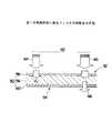
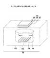
このNDフィルタを備えたカメラモジュールについて、図1及び図2を参照して説明する。図1及び図2は、NDフィルタを備えた従来のカメラモジュールを示している。このカメラモジュール2は、その入光側にNDフィルタ4が設置され、図1の例では、撮像素子6とレンズ8との間に赤外領域に光減衰特性を持つIR(Infra Red )カットフィルタ10が設置され、図2の例では、レンズ8の入光側にIRカットフィルタ10が設置されている。このような構造において、NDフィルタ4は、携帯電話機やディジタルカメラの筐体に設置され、撮像素子6に強い光が入射するのを抑制している。 A camera module including the ND filter will be described with reference to FIGS. 1 and 2 show a conventional camera module having an ND filter. The
ところで、光学系に用いられるフィルタや光減衰器に関し、次のような先行特許文献が存在している。
また、特開平8−136736号公報(特許文献2)には、光減衰器とその製造方法に関し、各種ドーパントとして、マンガン(Mn)、ニッケル(Ni)、クロム(Cr)、バナジウム(V)、コバルト(Co)、鉄(Fe)、銅(Cu)が用いられ、これらドーパントについて波長と損失の関係が開示されている。図3はこれらドーパントが入光波長に対して固有の損失を生じさせることを示している。
JP-A-8-136736 (Patent Document 2) relates to an optical attenuator and a method for producing the same, and various dopants include manganese (Mn), nickel (Ni), chromium (Cr), vanadium (V), Cobalt (Co), iron (Fe), and copper (Cu) are used, and the relationship between wavelength and loss is disclosed for these dopants. FIG. 3 shows that these dopants cause inherent losses with respect to the incident wavelength.
ところで、図1及び図2に示すように、NDフィルタ4を設置すると、強い光が撮像素子6に入るのを規制し、スミア現象による画質劣化を防止できるものの、NDフィルタ4がカメラモジュール2の入光側に設置されているため、NDフィルタ4の厚さ分だけ携帯電話機等の筐体部が厚くなるという欠点があった。また、NDフィルタ4を筐体部に装着すれば、そのフィルタ構成が複雑化するとともに、その設置構造がコスト高になる。 By the way, as shown in FIGS. 1 and 2, when the
また、従来のフィルタについて、図4を参照して説明する。図4は、従来のフィルタを示す断面図である。このフィルタ12は、透明な基板14の一面部に蒸着IRカットフィルタ層16を設置し、その他面部に蒸着NDフィルタ層18を設置したものである。これら蒸着IRカットフィルタ層16及び蒸着NDフィルタ層18は、蒸着膜による反射タイプのフィルタを構成している。このフィルタ12の目的とするところは、到来する光20に対し、赤外光22は蒸着IRカットフィルタ層16で反射することにより撮像素子6への到達を阻止し、また、到来する光20に含まれる可視光24は蒸着IRカットフィルタ層16及び基板14を通過し、その一部を蒸着NDフィルタ層18の内面側で反射させて減衰させた後、撮像素子6に到達させるものである。 A conventional filter will be described with reference to FIG. FIG. 4 is a cross-sectional view showing a conventional filter. This
ところで、このフィルタ12を用いた撮影装置について、図5を参照して説明する。図5は、フィルタ12を用いた撮影装置の概要を示している。この撮影装置26には、筐体28の内部に撮像素子6及びレンズ8が設置されているとともに、その入光面側にフィルタ12が設置されている。このフィルタ12は既述の構成である。そして、フィルタ12の前面側には筐体28によって支持された透明パネル部30を備えている。 Now, a photographing apparatus using the
被写体32からの光34は透明パネル部30、フィルタ12及びレンズ8を通過し、その減衰光36により撮像素子6に被写体32の画像38を結像させる。また、被写体32からの光34の一部は、蒸着IRカットフィルタ層16の内面側で反射光40を生じ、その反射光40は、フィルタ12の蒸着IRカットフィルタ層16を通過して蒸着NDフィルタ層18で反射し、透明パネル部30の内面側で反射した後、フィルタ12及びレンズ8を通過し、撮像素子6に被写体32の虚像(ゴースト)42を結像させる。44、46は反射部分を示し、多重反射により形成される虚像(ゴースト)42が画像38を劣化させる。 Light 34 from the
このような基板14の表面側に形成された蒸着膜である蒸着IRカットフィルタ層16、その裏面側に同種の蒸着NDフィルタ層18を備えるフィルタ12では、蒸着NDフィルタ層18側で反射44を生じ、筐体28側の透明パネル部30で反射46を生じるので、斯かる構成では、虚像42の発生を避けることができず、画像品質を低下させるため、実用性に乏しい。 In the
このようなフィルタ12について、反射44、46を防止するには、光34の透過効率を向上させて多重反射を抑制させればよいが、蒸着NDフィルタ層18は蒸着処理によって鏡面膜を構成しており、この鏡面膜上に例えば、蒸着IRカットフィルタ層等、他のフィルタ層を形成することは、蒸着NDフィルタ層18が持つ本来のフィルタ機能を損ない、無意味なものとするため、採用できない。 In order to prevent the
また、フィルタ12の蒸着IRカットフィルタ層16の表面に他のフィルタ層を形成することも、蒸着IRカットフィルタ層16が持つ本来のフィルタ機能を損ない、無意味なものとするため、同様に採用できない。 Further, the formation of another filter layer on the surface of the deposited IR
また、絞り機構を備えない光学系では、被写体等から到来する強い光の影響を回避し、機械的に調整することが不可能である。 In addition, in an optical system that does not include an aperture mechanism, it is impossible to perform mechanical adjustment while avoiding the influence of strong light coming from a subject or the like.
このような課題や知見に関し、上記特許文献1、2等に開示はなく、その解決手段の開示や示唆はない。 Regarding such problems and knowledge, there is no disclosure in the above-mentioned
そこで、本発明は、光学系に用いられるフィルタに関し、画像劣化を防止することを第1の目的とする。 Therefore, the present invention relates to a filter used in an optical system, and a first object is to prevent image deterioration.
また、本発明は、光学系のフィルタ構成の簡略化を実現したフィルタ、その製造方法、撮像装置及び電子装置を提供することを第2の目的とする。
In addition, a second object of the present invention is to provide a filter that realizes a simplified filter configuration of an optical system, a manufacturing method thereof, an imaging device, and an electronic device.
上記目的を達成するため、本発明のフィルタは、遷移金属を含有させたことにより、透過する光の赤外領域に対する遮断機能と可視光領域に対する減衰機能とを有する基板部(56)と、この基板部の表面又は裏面の一方又は双方に成膜されて光の反射を抑制する反射抑制膜(ARコート層58、60)とを備える構成である。 In order to achieve the above object, the filter of the present invention comprises a substrate (56) having a blocking function with respect to an infrared region of transmitted light and an attenuation function with respect to a visible light region by including a transition metal, It is a structure provided with the reflection suppression film | membrane (
斯かる構成とすれば、基板部に遷移金属を含有させたことにより、基板部では、透過する光の赤外領域を遮断し、可視光領域を減衰させる。また、基板部の表面又は裏面の一方又は双方に形成された反射抑制膜で光の反射を抑制する。これにより、単一のフィルタを以て赤外光を遮断しつつ強い光線の通過を防止し、同時に反射を抑制することが可能である。 With such a configuration, the transition metal is contained in the substrate portion, whereby the substrate portion blocks the infrared region of the transmitted light and attenuates the visible light region. Further, reflection of light is suppressed by a reflection suppressing film formed on one or both of the front surface and the back surface of the substrate portion. As a result, it is possible to prevent the passage of strong light while blocking infrared light with a single filter and to suppress reflection at the same time.
上記目的を達成するため、本発明のフィルタの製造方法は、基材に遷移金属を添加して赤外領域に対する遮断機能と可視光領域に対する減衰機能とを有する基板部を形成する処理と、前記基板部の表面又は裏面の一方又は双方に光の反射を抑制する反射抑制膜を成膜する処理とを含む構成である。 In order to achieve the above object, a method for producing a filter according to the present invention includes a process of forming a substrate having a blocking function for an infrared region and an attenuation function for a visible light region by adding a transition metal to a base material, And a process of forming a reflection suppression film that suppresses reflection of light on one or both of the front surface and the back surface of the substrate portion.
斯かる製造方法では、基材として例えば、合成樹脂又はガラスを用いて、この基材に赤外領域を遮断させるとともに可視光領域を減衰させる遷移金属を含有させて基板部を形成する。この基板部の表面部に対し、その表面又は裏面の一方又は双方に光反射抑制材料の蒸着又は塗布等により反射抑制膜を形成する。この結果、基板部を通過する光の赤外光を遮断し、可視光を減衰させ、また、基板部に設置された反射抑制膜で光の反射が抑制される。 In such a manufacturing method, for example, synthetic resin or glass is used as a base material, and the base material portion is formed by containing a transition metal that blocks the infrared region and attenuates the visible light region. A reflection suppressing film is formed on one or both of the front surface and the back surface of the substrate portion by vapor deposition or application of a light reflection suppressing material. As a result, the infrared light of the light passing through the substrate portion is blocked, the visible light is attenuated, and the reflection of light is suppressed by the antireflection film installed on the substrate portion.
上記目的を達成するため、本発明の撮像装置は、撮像素子(78)とともにフィルタ(50)を備える撮像装置であって、前記フィルタが、遷移金属を含有させたことにより、透過する光の赤外領域に対する遮断機能と可視光領域に対する減衰機能とを有する基板部(56)と、この基板部の表面又は裏面の一方又は双方に成膜されて光の反射を抑制する反射抑制膜(ARコート層58、60)とを備える構成である。即ち、この撮像装置は、撮像素子の入光側に既述のフィルタを備えた構成であり、斯かるフィルタによって赤外光を遮断しつつ強い光線の通過を防止し、同時に反射を抑制することができる。従って、撮像素子にはスミア現象等による画像劣化のない質の高い画像を検出し、結像させることができる。 In order to achieve the above object, an image pickup apparatus according to the present invention is an image pickup apparatus including a filter (50) together with an image pickup element (78). A substrate portion (56) having a blocking function with respect to the outer region and an attenuation function with respect to the visible light region, and a reflection suppressing film (AR coating) formed on one or both of the front surface and the back surface of the substrate portion to suppress
上記目的を達成するため、本発明の電子装置は、カメラモジュールを備える電子装置であって、前記カメラモジュールに内蔵され、又は前記カメラモジュールの入光側に設置されるフィルタが、遷移金属を含有させたことにより、透過する光の赤外領域に対する遮断機能と可視光領域に対する減衰機能とを有する基板部と、この基板部の表面又は裏面の一方又は双方に成膜されて光の反射を抑制する反射抑制膜とを備える構成である。この電子装置は、カメラモジュールを備える構成であって、既述のフィルタを用いたものである。斯かる構成によれば、赤外光を遮断しつつ強い光線がフィルタによって抑制され、同時に反射を抑制することができ、撮像素子にはスミア現象のない画像を結像させることができ、画像劣化を防止できる。 In order to achieve the above object, an electronic device of the present invention is an electronic device including a camera module, and the filter built in the camera module or installed on the light incident side of the camera module contains a transition metal. In this way, the substrate portion having a function of blocking transmitted light in the infrared region and a function of attenuating in the visible light region is formed on one or both of the front and back surfaces of the substrate portion, thereby suppressing light reflection. And a reflection suppressing film. This electronic apparatus has a camera module and uses the above-described filter. According to such a configuration, a strong light ray that blocks infrared light is suppressed by the filter, and reflection can be suppressed at the same time, and an image having no smear phenomenon can be formed on the image sensor, resulting in image degradation. Can be prevented.
上記目的を達成するためには、前記遷移金属は、ニッケル、コバルト、クロム、マンガン、バナジウム、鉄、銅、カーボン又はこれらの酸化物から選択された1又は2種以上で構成すればよい。斯かる遷移金属を含有させたフィルタは、既述の機能が得られる。
In order to achieve the above object, the transition metal may be composed of one or more selected from nickel, cobalt, chromium, manganese, vanadium, iron, copper, carbon, or oxides thereof. A filter containing such a transition metal can obtain the functions described above.
以上説明したように、本発明によれば、次のような効果が得られる。 As described above, according to the present invention, the following effects can be obtained.
(1) 本発明のフィルタによれば、遷移金属を含有させたことにより、赤外領域を遮断し可視光領域を減衰させる基板部を備えるとともに、その表面又は裏面の一方又は双方に光の反射を抑制する反射抑制膜を一体に備えた構成としたことから、赤外光を遮断しつつ強い光線を抑制し、同時に反射を抑制することができ、フィルタのコンパクト化を実現することができる。 (1) According to the filter of the present invention, by including a transition metal, the filter includes a substrate portion that blocks the infrared region and attenuates the visible light region, and reflects light on one or both of the front surface and the back surface. Since the reflection suppression film that integrally suppresses the light is integrated, it is possible to suppress strong light while blocking infrared light, and to suppress reflection at the same time, thereby realizing a compact filter.
(2) 本発明のフィルタの製造方法によれば、基材に遷移金属を添加して赤外領域を遮断し可視光領域を減衰させる基板部を形成し、この基板部の表面又は裏面の一方又は双方に光の反射を抑制する反射抑制膜を形成することにより、赤外光の遮断、可視光の減衰及び光の反射抑制の各機能を備えるフィルタを容易に製造することができる。 (2) According to the filter manufacturing method of the present invention, a transition metal is added to the base material to form a substrate portion that blocks the infrared region and attenuates the visible light region, and either the front surface or the back surface of the substrate portion is formed. Alternatively, by forming a reflection suppressing film that suppresses reflection of light on both sides, a filter having the functions of blocking infrared light, attenuating visible light, and suppressing reflection of light can be easily manufactured.
(3) 本発明の撮像装置によれば、単一のフィルタにより赤外光を遮断しつつ強い光線を抑制できるとともに、反射を抑制することができ、部品点数の削減、構造の簡略化、小型化を図ることができる。また、光学特性を一定に維持でき、スミアゴースト等による画像劣化のないクリアな画像特性を実現できる。 (3) According to the imaging device of the present invention, it is possible to suppress strong light while blocking infrared light with a single filter, and it is possible to suppress reflection, reduce the number of parts, simplify the structure, and reduce the size. Can be achieved. In addition, the optical characteristics can be kept constant, and clear image characteristics free from image degradation due to smear ghosts and the like can be realized.
(4) 本発明の電子装置によれば、単一のフィルタにより赤外光を遮断しつつ強い光線を抑制できるとともに反射を抑制することができ、部品点数の削減、構造の簡略化、小型化を図ることができ、また、光学特性を一定に維持でき、スミアゴースト等による画像劣化のない画像特性が得られ、クリアな撮影画像が得られる。
(4) According to the electronic device of the present invention, it is possible to suppress strong light while blocking infrared light with a single filter and to suppress reflection, and to reduce the number of components, simplify the structure, and reduce the size. In addition, the optical characteristics can be kept constant, image characteristics free from image degradation due to smear ghosts and the like can be obtained, and a clear captured image can be obtained.
第1の実施形態
本発明の第1の実施形態について、図6、図7及び図8を参照して説明する。図6は第1の実施形態に係るフィルタを示す斜視図、図7は図6の VII−VII 線に沿ったフィルタを示す一部省略断面図、図8はフィルタ機能を示す図である。First Embodiment A first embodiment of the present invention will be described with reference to FIG. 6, FIG. 7, and FIG. 6 is a perspective view showing the filter according to the first embodiment, FIG. 7 is a partially omitted sectional view showing the filter along the line VII-VII in FIG. 6, and FIG. 8 is a view showing the filter function.
このフィルタ50は、例えば、板状体に形成され、その表面を光を受ける受光面部52とすれば、その裏面を受光面部52に対応する出光面部54とする。このフィルタ50には、光を透過可能な例えば、透明な基板部56を備え、この基板部56は、石英ガラス又は合成樹脂を基材とし、ドーパントとして遷移金属を含有させて形成されている。基材に含有させる遷移金属は、基材が持つ光透過性に対し、赤外領域を遮断し、可視光領域を減衰させる物質として例えば、ニッケル(Ni)、コバルト(Co)、クロム(Cr)、マンガン(Mn)、バナジウム(V)、鉄(Fe)、銅(Cu)、カーボン(C)等や、これらの酸化物等であり、これら遷移金属から選択された1種又は2種以上が含有されている。ここで、遷移金属としては、赤外領域を遮断する遷移金属、可視光領域を減衰させる遷移金属とを組み合わせ、赤外領域を遮断し且つ可視光領域を減衰させる単一又は複数の遷移金属のいずれでもよい。そして、遷移金属の選択は、遷移金属が持つ光の波長に対する損失(図3)を参照し、所望の光学特性即ち、赤外領域の遮断、可視光領域の減衰量を想定し、1種又は2種以上を選択すればよい。その結果、所望の光学特性が基板部56に付与されることになる。 For example, if the
そして、この実施形態では、基板部56の表面部に設定された受光面部52及び出光面部54には、光の反射を抑制する反射抑制膜として、ARコート(Anti Reflection Coat)処理によりARコート層58、60が設置されている。ARコート層58、60は、例えば、フッ化マグネシウム(MgF2)、二酸化珪素(SiO2)等の無機化合物を真空蒸着やスパッタ法等のコート処理により形成され、光の反射及び乱反射防止処理膜を構成している。In this embodiment, the light receiving
斯かる構成とすれば、基板部56が持つ赤外領域を遮断するIRカットフィルタ機能と、可視光領域を減衰させるNDフィルタ機能との双方を備えることにより得られる第1のフィルタF1と、ARコート層58、60が持つ光反射防止機能で得られる第2のフィルタF2とを具備する(図9)。これら第1及び第2のフィルタF1、F2は単一の基板部56からなるフィルタ50により構成されている。従って、斯かる構成のフィルタ50によれば、赤外領域の遮断、可視光領域の減衰、反射防止の複合的な機能が単一のフィルタ50により実現されている。With such a configuration, the first filter F1 obtained by providing both the IR cut filter function for blocking the infrared region of the
これらの機能について、図8を参照して説明すると、赤外領域から可視光領域に分布する強力な光62が受光面部52に到来し、この光62において、64を赤外光、66を可視光とすれば、赤外光64はARコート層58を通過して基板部56に入るが、基板部56の遷移金属が持つ赤外領域の遮断機能により遮断され、ARコート層60を通過して出光面部54から出ることはない。また、可視光66はARコート層58を通過して基板部56に入るが、ARコート層58を通過して基板部56に達し、基板部56の遷移金属が持つ可視光領域の減衰機能により減衰を生じ、出光面部54から適正な強さの可視光68として出光することになる。そして、フィルタ50に一体に構成されたARコート層58による反射、ARコート層60の内面側での光反射も防止される。 When these functions are described with reference to FIG. 8,
斯かるフィルタ50によれば、従前に必要であったNDフィルタ、IRカットフィルタの複数枚からなる構成が単一のフィルタ構成となり、フィルタ構成の簡略化とともに、従前のフィルタ12(図4、図5)で生じた光反射による不都合も解消される。 According to such a
第2の実施形態
本発明の第2の実施形態について、図9を参照して説明する。図9は第2の実施形態に係るフィルタの製造方法を工程順に示した断面図である。Second Embodiment A second embodiment of the present invention will be described with reference to FIG. FIG. 9 is a cross-sectional view showing the method of manufacturing the filter according to the second embodiment in the order of steps.
既述したフィルタ50について、その製造方法は基板形成工程及びARコート層形成工程を含んでいる。 The manufacturing method of the
(1) 基板形成工程
基板部56は、基材に遷移金属を含有させて成形することにより形成される。図9の(A)は、成形後の基板部56の断面を示している。基板部56を構成するためのベースとなる基材は、ポリカーボネート等の合成樹脂、石英ガラスのいずれでもよい。また、ドーパントである遷移金属は、既述したように、基材が持つ光透過性に対し、赤外領域を遮断し、可視光領域を減衰させる物質である。この種の遷移金属は例えば、ニッケル(Ni)、コバルト(Co)、クロム(Cr)、マンガン(Mn)、バナジウム(V)、鉄(Fe)、銅(Cu)、カーボン(C)等や、これらの酸化物等から選択された1種又は2種以上である。これら遷移金属の選択は、遷移金属が持つ光の波長に対する損失(図3)を参照し、所望の光学特性即ち、赤外領域の遮断、可視光領域の減衰量を想定し、1種又は2種以上を選択すればよい。その結果、所望の光学特性が基板部56に付与されることになる。基材を合成樹脂で構成した場合、これらの遷移金属は、その基材中に添加物として存在し、また、基材を石英ガラスで構成した場合、これらの遷移金属はイオン化されて存在することになる。遷移金属がいずれの形態であっても、透過する光のエネルギを吸収し、赤外領域の遮断、可視光領域の減衰に寄与することになる。この実施形態では、基材にポリカーボネートを選択し、このポリカーボネートに赤外領域を遮断する遷移金属としてコバルト(Co)、可視光領域を減衰させる遷移金属としてクロム(Cr)を含有させて基板部56を形成した。(1) Substrate Formation Step The
(2) ARコート層形成工程
基板形成工程で得られた基板部56は、合成樹脂板又は石英ガラス板の形態である。そこで、この基板部56の表面にARコート処理を施し、ARコート層58、60を形成する。コート剤には、例えば、フッ化マグネシウム(MgF2)、二酸化珪素(SiO2)等の無機化合物が用いられる。また、コート処理は、乾式法又は湿式法のいずれでもよく、乾式法としては、真空蒸着法、スパッタ法又はCVD法のいずれでもよく、また、湿式法を用いる場合には、塗布法又はゾルゲル法のいずれでもよい。この実施形態では、図9の(B)に示すように、真空雰囲気70内に基板部56を維持し、コート剤として例えば、フッ化マグネシウム72を選択し、真空蒸着処理により、基板部56にコート処理を施した。(2) AR Coat Layer Formation Step The
このコート処理により、図9の(C)に示すように、基板部56の表面部にはARコート層58、60が形成され、フィルタ50が構成される。 By this coating treatment, as shown in FIG. 9C, AR coating layers 58 and 60 are formed on the surface portion of the
このような処理工程により形成されたフィルタ50は、遷移金属を含有させて赤外領域を遮断し可視光領域を減衰させる基板部56によって第1のフィルタF1、ARコート層58、60によって第2のフィルタF2を構成し、フィルタF1では赤外領域を遮断し可視光領域を減衰させる機能、フィルタF2では反射防止機能を備えている。即ち、単一のフィルタ50によって異なる複合的なフィルタ機能が実現されているのである。The
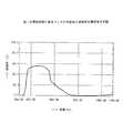
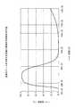
この実施形態に係るフィルタの光学特性について、図10及び図11を参照して説明する。図10は、第1の実施形態に係るフィルタの波長に対する透過率を示し、図11は、比較例として従来のフィルタ特性を示している。 The optical characteristics of the filter according to this embodiment will be described with reference to FIGS. FIG. 10 shows the transmittance with respect to the wavelength of the filter according to the first embodiment, and FIG. 11 shows a conventional filter characteristic as a comparative example.
このフィルタは、例えば、基材にポリカーボネートを使用し、この基材に赤外領域を遮断する遷移金属としてコバルト(Co)、可視光領域を減衰させる遷移金属としてクロム(Cr)を含有させて基板を形成し、フッ化マグネシウムからなるARコート層を備えたものである。 For example, this filter uses polycarbonate as a base material, and this base material contains cobalt (Co) as a transition metal that blocks the infrared region, and chromium (Cr) as a transition metal that attenuates the visible light region. And an AR coating layer made of magnesium fluoride.
このようなフィルタでは、図10に示すように、可視光領域の透過率は60パーセント以下に抑えられ、赤外領域の透過率は20パーセント以下に抑えられるとともに、波長700〔nm〕以上の光では10パーセント以下の無視できる程度の透過率となっている。従来の赤外領域のみを遮断領域とするフィルタ(図4)が持つフィルタ特性に比較し、実施形態に係るフィルタでは、可視光領域に著しい減衰機能が得られている。このような単一のフィルタによって可視光領域の減衰機能と、赤外領域の遮断機能とを備えたことにより、強い光に対して適正な光量を得ることが理解されよう。また、ARコート層58、60による反射防止機能が加わり、反射も抑えることができる優れたフィルタ特性が得られる。 In such a filter, as shown in FIG. 10, the transmittance in the visible light region is suppressed to 60% or less, the transmittance in the infrared region is suppressed to 20% or less, and light having a wavelength of 700 nm or more is used. In this case, the transmittance is negligible at 10% or less. Compared to the filter characteristics of the filter (FIG. 4) having the conventional infrared region only as the blocking region (FIG. 4), the filter according to the embodiment has a remarkable attenuation function in the visible light region. It will be understood that such a single filter provides an attenuation function in the visible light region and a blocking function in the infrared region, thereby obtaining an appropriate amount of light for strong light. In addition, an antireflection function by the AR coating layers 58 and 60 is added, and excellent filter characteristics that can suppress reflection can be obtained.
第3の実施形態
本発明の第3の実施形態について、図12、図13及び図14を参照して説明する。図12は第3の実施形態に係る撮像装置を示す図、図13は撮像素子の出力特性、図14はフィルタを備える撮像素子の出力特性を示している。Third Embodiment A third embodiment of the present invention will be described with reference to FIG. 12, FIG. 13, and FIG. FIG. 12 is a diagram showing an image pickup apparatus according to the third embodiment, FIG. 13 shows the output characteristics of the image sensor, and FIG. 14 shows the output characteristics of the image sensor provided with a filter.
撮像装置の一例である撮像センサ74には、光76の入光部に既述のフィルタ50が設置され、このフィルタ50を通過した光76を撮像素子78で受ける構成である。この場合、入光部側に光学レンズを設置してもよい。フィルタ50は、既述の通り、光を透過可能な例えば、透明な基板部56を石英ガラス又は合成樹脂を基材とし、ドーパントとして前記遷移金属を含有させて形成し、基板部56の表面部に設定された受光面部52及び出光面部54にARコート層58、60を設置したものである。また、撮像素子78は、固体撮像素子として例えば、CCD素子で構成されている。 An
斯かる構成において、撮像素子78が持つ出力特性(図13)について、Rは赤、Gは緑、Bは青を示している。また、フィルタ50は、図10に示す波長に対する透過率を備えているものとすれば、フィルタ50を通過した光76を受光する撮像素子78の出力Voは、フィルタ50を設置しない撮像素子78の出力にフィルタ50が持つ透過率ηを乗算して得られる値となる。即ち、フィルタ50を設置した場合、図14に示すように、出力特性が変化し、フィルタ50が持つ透過率ηに応じて、可視光領域の出力レベルは約50パーセントに低下し、強い光が所望のレベルに減衰されるとともに、赤外領域が遮断されていることが理解されよう。図14において、破線は比較のために示したフィルタ50の無い出力特性である。 In such a configuration, R represents red, G represents green, and B represents blue for the output characteristics (FIG. 13) of the
第4の実施形態
本発明の第4の実施形態について、図15を参照して説明する。図15は第4の実施形態に係る撮像装置の概要を示す図である。Fourth Embodiment A fourth embodiment of the present invention will be described with reference to FIG. FIG. 15 is a diagram illustrating an outline of an imaging apparatus according to the fourth embodiment.
撮像装置の一例であるカメラモジュール80は、既述の撮像センサ74の構成であるフィルタ50及び撮像素子78を備え、フィルタ50の入光部側にレンズ82が設置されて構成されている。撮像センサ74のフィルタ50及び撮像素子78は既述の通り(第3の実施形態)である。 A
斯かる構成とすれば、被写体からの光76がレンズ82及びフィルタ50を通して撮像素子78に入光し、撮像素子78に被写体を表す結像が得られる。撮像センサ74について説明したように、このカメラモジュール80においても、被写体側から強い光76がカメラモジュール80に入光すると、その光76に含まれる可視光領域の光はフィルタ50の基板部56側のフィルタ機能により減衰し、赤外領域の光は基板部56側のフィルタ機能により遮断される。このような基板部56が持つ第1のフィルタ機能に対し、フィルタ50の表面部にはARコート層58、60が持つ第2のフィルタ機能により光反射が抑制される。この結果、撮像素子78には赤外領域の遮断と適正な光レベルによって被写体の画像が得られるとともに、スミア現象によるゴースト(虚像)の結像がなく、クリアな画像出力が得られる。 With such a configuration, light 76 from the subject enters the
第5の実施形態
本発明の第5の実施形態について、図16を参照して説明する。図16は第5の実施形態に係る撮像装置の概要を示す図である。Fifth Embodiment A fifth embodiment of the present invention will be described with reference to FIG. FIG. 16 is a diagram illustrating an outline of an imaging apparatus according to the fifth embodiment.
撮像装置の一例であるカメラモジュール84は、既述のカメラモジュール80(図15)のレンズ82をフィルタ50と撮像素子78の間に設置して構成されたものである。 A
斯かる構成とすれば、フィルタ50を通過させた光76がレンズ82を通して撮像素子78に被写体を表す結像を生じさせる。レンズ82の後にフィルタ50を設置した場合(図15)、レンズ82の前にフィルタ50を設置した場合のいずれの場合もフィルタ50がレンズ82の結像機能に何ら影響を与えることなく、同様に適正な光レベルに調整された被写体の画像が得られるとともに、スミア現象によるゴーストの結像を防止でき、撮像素子78にはクリアな画像出力が得られる。 With such a configuration, the light 76 that has passed through the
第6の実施形態
本発明の第6の実施形態について、図17を参照して説明する。図17は第6の実施形態に係る撮像装置の外観を示す斜視図である。上記実施形態と同一部分には同一符号を付してある。Sixth Embodiment A sixth embodiment of the present invention will be described with reference to FIG. FIG. 17 is a perspective view illustrating an appearance of an imaging apparatus according to the sixth embodiment. The same parts as those in the above embodiment are given the same reference numerals.
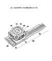
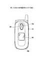
撮像装置の一例であるカメラモジュール84は、携帯電話機、PDA、ノート型パーソナルコンピュータ等の情報端末、ディジタルカメラ等の電子機器の筐体に搭載されて用いられる。このカメラモジュール84は、鏡筒としての筐体86を備え、この筐体86の内部に既述したフィルタ50、レンズ82及び撮像素子78が設置された構成である。フィルタ50、レンズ82及び撮像素子78の配置は既述の構成(図16)と同様である。この筐体86の背面部には回路基板88が設置され、この回路基板88に搭載されたセンサ回路90にはフレキシブル基板92が接続されている。フィルタ50、撮像素子78及びレンズ82は既述した通りの構成である。そして、この実施形態では、筐体86には入光窓94を包囲するカバーリング96が設置されている。 A
斯かる構成とすれば、図示しない被写体からの光76が入光窓94からフィルタ50に入光し、レンズ82によって集光された後、撮像素子78に被写体を表す結像が得られ、その結像出力がセンサ回路90で検出され、その検出出力がフレキシブル基板92を通して出力される。 With such a configuration, light 76 from a subject (not shown) enters the
このような撮像処理において、フィルタ50では、被写体からの赤外領域が遮断され、可視光領域のレベルが適正レベルに減衰される。また、フィルタ50では、既述したARコート層58、60(図16等)により光反射が抑制され、撮像素子78には虚像の無いクリアな画像が結像される。また、このカメラモジュール84では、フィルタ50が赤外領域の遮断、可視光領域の減衰、光反射、光乱反射を抑制しており、単一のフィルタ50でこれらの機能が実現されていることから、筐体86の高さを抑えることができ、設置される携帯電話機、PDA、ノート型パーソナルコンピュータ等の情報端末、ディジタルカメラ等の電子機器の筐体の薄型化に寄与することができる。 In such an imaging process, the
第7の実施形態
本発明の第7の実施形態について、図18を参照して説明する。図18は第7の実施形態に係る撮影装置の概要を示す図である。Seventh Embodiment A seventh embodiment of the present invention will be described with reference to FIG. FIG. 18 is a diagram showing an outline of an imaging apparatus according to the seventh embodiment.
この撮影装置98は、カメラモジュール等の撮像装置を備えて被写体からの光を受け、被写体を表す画像情報を発生させるものであって、例えば、ディジタルカメラとして構成され、又は携帯電話機、PDA、ノート型パーソナルコンピュータ等の情報端末等の電子機器に搭載され、この実施形態では、カメラモジュール100を備えるとともに、その入光部側に既述のフィルタ50を備えたものである。このフィルタ50は、撮影装置98の筐体部又は電子装置の筐体部102に設置され、入光部側の保護パネル部を構成している。このように、フィルタ50を筐体部102側に設置したことから、この実施形態に係るカメラモジュール100は、撮像素子78及びレンズ82からなる構成であって、撮像素子78の入光部側にレンズ82を設置したものである。フィルタ50は既述の構成(図7)を備えており、撮像素子78は既述の通りである。 The photographing
斯かる構成とすれば、保護パネル部を構成するフィルタ50を通過させた光がカメラモジュール100のレンズ82を通して撮像素子78に被写体を表す結像を生じさせる。フィルタ50は被写体からの光を適正な光レベルに調整し、撮像素子78には被写体の画像が得られるとともに、スミア現象によるゴーストの結像を防止でき、クリアな画像出力が得られる。そして、フィルタ50は、赤外領域の遮断、可視光領域の減衰、光の反射や乱反射を防止する機能に加え、保護パネル部を兼用することから、撮影装置98の部品点数の削減とともに、その薄型化、小型化に寄与する。 With such a configuration, the light that has passed through the
第8の実施形態
本発明の第8の実施形態について、図19〜図23を参照して説明する。図19は第8の実施形態に係る携帯電話機を示す正面図、図20は閉じた状態の携帯電話機を示す平面図、図21は閉じた状態の携帯電話機の一部断面図、図22は開いた状態の携帯電話機を示す側面図である。Eighth Embodiment An eighth embodiment of the present invention will be described with reference to FIGS. FIG. 19 is a front view showing a mobile phone according to an eighth embodiment, FIG. 20 is a plan view showing the mobile phone in a closed state, FIG. 21 is a partial sectional view of the mobile phone in a closed state, and FIG. It is a side view which shows the mobile phone of the state.
この携帯電話機104は既述の電子装置の一例であって、第1の筐体部106と第2の筐体部108とを備え、これら筐体部106、108をヒンジ部110を中心に回動することにより開閉可能に構成したものである。筐体部106にはシャッターボタン112を含む複数のキーを備える操作部114等が設置され、筐体部108にはファインダーを兼ねる第1の表示部116等が設置されている。表示部116はLCD(Liquid Crystal Display)表示器で構成されている。 The
筐体部108の背面部には、図20に示すように、カメラモジュール84(図17)が組み込まれているとともに、閉じられた状態でファインダーを構成する第2の表示部118が設置されている。カメラモジュール84は既述の通りであり、図16を参照して説明した通りである。また、表示部118はLCD表示器で構成されている。 As shown in FIG. 20, a camera module 84 (FIG. 17) is incorporated in the rear surface of the
カメラモジュール84は、図21に示すように、筐体部108を構成する前面ケース部120と背面ケース部122との間に挟み込まれるように内蔵されており、背面ケース部122に形成された受光窓124には保護パネル部125が設置されている。この保護パネル部125をフィルタ50で構成してもよい。 As shown in FIG. 21, the
斯かる構成とすれば、筐体部106、108を閉じた状態では、カメラモジュール84のフィルタ50を通して受光される被写体からの光によりレンズ82(図16)を通して撮像素子78(図16)に被写体を表す画像が結像され、その画像出力として表示部118に被写体を表す画像が表示される。フィルタ50は既述の通り、赤外領域の遮断、可視光領域の減衰及び光反射や乱反射を防止する機能を備えているので、強い光は適正レベルに調整され、スミア現象によるゴースト等の画像劣化のないクリアな画像が得られる。また、カメラモジュール84ではフィルタ構成が簡略化及び薄型化されているので、携帯電話機104の薄型化が図られる。そして、シャッターボタン112の操作により、その画像データを記憶部に取り込むことができる。 With such a configuration, when the
また、筐体部106、108を開いた状態(図22)では、同様にカメラモジュール84のフィルタ50を通して撮像素子78(図16)に被写体を表す画像が結像され、その画像出力として表示部116に被写体を表す画像が表示される。同様にシャッターボタン112の操作により、その画像データを記憶部に取り込むことができる。 In the state where the
第9の実施形態
本発明の第9の実施形態について、図23を参照して説明する。図23は第9の実施形態に係るノート型パーソナルコンピュータを示す斜視図である。Ninth Embodiment A ninth embodiment of the present invention will be described with reference to FIG. FIG. 23 is a perspective view showing a notebook personal computer according to the ninth embodiment.
このノート型パーソナルコンピュータ126は既述の電子装置の一例であって、第1の筐体部128と第2の筐体部130とを備えており、これら筐体部128、130をヒンジ部132を中心に回動することにより開閉可能に構成したものである。筐体部128には、シャッターボタンを含む複数のキーを備える操作部134等を備え、筐体部130にはファインダーを兼ねる表示部136等が設置されている。表示部136はLCD(Liquid Crystal Display)表示器で構成されている。 The notebook
そして、カメラモジュール84は、筐体部130の表示部136に隣接して設置され、筐体部130に組み込まれている。カメラモジュール84の前面には保護パネル部を兼ねる既述のフィルタ50が設置されている。 The
斯かる構成とすれば、撮影モードの実行により、カメラモジュール84の撮像素子78(図16)にはフィルタ50を通して取り込まれた画像が結像され、表示部136に表示される。フィルタ50は既述の通り、赤外領域の遮断、可視光領域の減衰及び光反射や乱反射を防止する機能を備えているので、強い光は適正レベルに調整され、スミア現象によるゴースト等の画像劣化のないクリアな画像が得られる等、上記実施形態と同様の効果が得られる。また、カメラモジュール84ではフィルタ構成が簡略化及び薄型化されているので、カメラモジュール84が設置されている筐体部130の薄型化に寄与する。 With such a configuration, an image captured through the
第10の実施形態
本発明の第10の実施形態について、図24を参照して説明する。図24は第10の実施形態に係るPDA(personal digital assistant)を示す斜視図である。Tenth Embodiment A tenth embodiment of the present invention will be described with reference to FIG. FIG. 24 is a perspective view showing a PDA (personal digital assistant) according to the tenth embodiment.
このPDA138は情報端末であって、既述の電子装置を構成している。このPDA138では中央部にファインダーを兼ねる表示部140、その上部側にカメラモジュール84、表示部140の側面部にシャッターボタン142を備えている。 The
このようなPDA138においても、カメラモジュール84に既述のフィルタ50を備えたので、既述の通り、赤外領域の遮断、可視光領域の減衰及び光反射や乱反射を防止する機能を備えているので、強い光は適正レベルに調整され、スミア現象によるゴースト等の画像劣化のないクリアな画像が得られる等、上記実施形態と同様の効果が得られる。また、カメラモジュール84ではフィルタ構成が簡略化及び薄型化されているので、カメラモジュール84が設置されている筐体部144の薄型化に寄与する。 Also in such a
以上説明した実施形態について、その特徴事項や利点、変形例等を以下に列挙する。 With respect to the embodiment described above, features, advantages, modifications, and the like are listed below.
(1) ディジタルカメラ等の撮影装置に使用するIRカットフィルタではNDフィルタの特性が併用され、従来のNDフィルタではガラス基板の表面に蒸着膜を形成しているため、フィルタ表面の乱反射防止のためのARコート処理が困難であり、膜密着が悪いためカメラ等の光学系のフィルタとしては実用性に乏しいものであったが、本発明に係るフィルタでは、既述の実施形態に記載の通り、基材としてガラス又は合成樹脂にND特性及びIR特性を有する化学成分を含有させたことにより、基板部が赤外領域の遮断機能及び可視光領域の減衰機能を備えるとともに、その基板部の表面部にARコート処理が可能となり、ARコート層により光の反射、乱反射を抑制することができる。即ち、単一の基板部からなるフィルタにより、赤外光の遮断(IRカットフィルタ機能)、可視光の減衰(NDフィルタ機能)及びAR機能の各機能を同時に実現することができる。具体的には、人間の目に見える可視光(約450nm〜650nm)の光はそのNDフィルタ機能により適正光量まで光が吸収され、減衰させることができ、人間の目に見えない赤外光(700nm以上)の光はIRカットフィルタ機能により吸収し除去することができる。斯かるフィルタを備えた撮像センサやカメラモジュールでは、撮像素子に適正光量の可視光を受けることができ、正常な画像が得られる。 (1) IR cut filters used in digital camera and other imaging devices use the characteristics of ND filters. Conventional ND filters have a deposited film formed on the surface of a glass substrate. The AR coating treatment is difficult and the film adhesion is poor, so it was poor in practicality as a filter for an optical system such as a camera, but in the filter according to the present invention, as described in the above-described embodiment, By including a chemical component having ND characteristics and IR characteristics in glass or synthetic resin as a base material, the substrate portion has an infrared region blocking function and a visible light region attenuation function, and the surface portion of the substrate portion. In addition, AR coating treatment can be performed, and reflection and diffuse reflection of light can be suppressed by the AR coating layer. In other words, the filter composed of a single substrate portion can simultaneously realize the functions of blocking infrared light (IR cut filter function), attenuation of visible light (ND filter function), and AR function. Specifically, visible light (approximately 450 nm to 650 nm) visible to the human eye can be attenuated to an appropriate amount by the ND filter function, and can be attenuated. 700 nm or more light can be absorbed and removed by the IR cut filter function. In an image sensor or camera module provided with such a filter, the image sensor can receive an appropriate amount of visible light, and a normal image can be obtained.
(2) 既述のフィルタを用いれば、単一のフィルタでIRカットフィルタとNDフィルタを一体化構成とすることができ、コスト低減を図ることができる。 (2) If the above-described filter is used, the IR cut filter and the ND filter can be integrated with a single filter, and the cost can be reduced.
(3) カメラモジュールでは、従前のNDフィルタの設置が不要となり、偏平化、小型化を図ることができる。 (3) The camera module does not require a conventional ND filter and can be flattened and downsized.
(4) また、既述のフィルタでは、IRカットフィルタとNDフィルタを1つにし、ARコート処理が可能であるから、光学特性を一定に維持できるとともに、ゴーストのないクリアな画像特性が得られる。 (4) In addition, since the IR filter can be performed with the IR cut filter and the ND filter in the above-described filter, the optical characteristics can be kept constant and a clear image characteristic without ghost can be obtained. .
(5) 上記実施形態では、基板部56の表面側にARコート層58、裏面側にARコート層60を設置した構成について開示したが、ARコート層58、60の一方のみとし、基板部56の表面又は裏面側で光反射を抑制する構成としてもよい。 (5) In the above-described embodiment, the configuration in which the
(6) 撮像装置として撮像センサ、カメラモジュールにおいて、基板部56に含有させる遷移金属の種類や添加量を異ならせ、光の減衰量を調整した複数のフィルタ50を使用すれば、赤外光の遮断機能を備えるとともに、絞り機構と同等の光学特性を実現することができる。 (6) In an imaging sensor or camera module as an imaging device, if a plurality of
次に、以上述べた本発明のフィルタ、その製造方法、撮像装置及び電子装置の各実施形態から抽出される技術的思想を請求項の記載形式に準じて付記として列挙する。本発明に係る技術的思想は上位概念から下位概念まで、様々なレベルやバリエーションにより把握できるものであり、以下の付記に本発明が限定されるものではない。 Next, technical ideas extracted from the embodiments of the filter of the present invention, the manufacturing method thereof, the imaging device, and the electronic device described above are listed as appendices according to the description format of the claims. The technical idea according to the present invention can be grasped by various levels and variations from a superordinate concept to a subordinate concept, and the present invention is not limited to the following supplementary notes.
(付記1) 遷移金属を含有させたことにより、透過する光の赤外領域に対する遮断機能と可視光領域に対する減衰機能とを有する基板部と、
この基板部の表面又は裏面の一方又は双方に成膜されて光の反射を抑制する反射抑制膜と、
を備えることを特徴とするフィルタ。(Supplementary Note 1) By including a transition metal, a substrate portion having a blocking function for the infrared region of transmitted light and an attenuation function for the visible light region;
A reflection suppressing film which is formed on one or both of the front surface and the back surface of the substrate portion and suppresses reflection of light;
A filter comprising:
(付記2) 基材に遷移金属を添加して赤外領域に対する遮断機能と可視光領域に対する減衰機能とを有する基板部を形成する処理と、
前記基板部の表面又は裏面の一方又は双方に光の反射を抑制する反射抑制膜を成膜する処理と、
を含むことを特徴とするフィルタの製造方法。(Additional remark 2) The process which forms the board | substrate part which has the interruption | blocking function with respect to an infrared region, and the attenuation | damping function with respect to a visible region by adding a transition metal to a base material,
Processing to form a reflection suppressing film for suppressing reflection of light on one or both of the front surface and the back surface of the substrate portion;
The manufacturing method of the filter characterized by including.
(付記3) 撮像素子とともにフィルタを備える撮像装置であって、前記フィルタが、
遷移金属を含有させたことにより、透過する光の赤外領域に対する遮断機能と可視光領域に対する減衰機能とを有する基板部と、
この基板部の表面又は裏面の一方又は双方に成膜されて光の反射を抑制する反射抑制膜と、
を備える構成としたことを特徴とする撮像装置。(Additional remark 3) It is an imaging device provided with a filter with an image pick-up element, Comprising: The said filter,
By including a transition metal, a substrate portion having a blocking function for the infrared region of transmitted light and an attenuation function for the visible light region;
A reflection suppressing film which is formed on one or both of the front surface and the back surface of the substrate portion and suppresses reflection of light;
An image pickup apparatus comprising:
(付記4) カメラモジュールを備える電子装置であって、
前記カメラモジュールに内蔵され、又は前記カメラモジュールの入光側に設置されるフィルタが、
遷移金属を含有させたことにより、透過する光の赤外領域に対する遮断機能と可視光領域に対する減衰機能とを有する基板部と、、
この基板部の表面又は裏面の一方又は双方に成膜されて光の反射を抑制する反射抑制膜と、
を備える構成としたことを特徴とする電子装置。(Appendix 4) An electronic device including a camera module,
A filter built in the camera module or installed on the light incident side of the camera module,
By including a transition metal, a substrate portion having a blocking function for the infrared region of transmitted light and an attenuation function for the visible light region,
A reflection suppressing film which is formed on one or both of the front surface and the back surface of the substrate portion and suppresses reflection of light;
An electronic device characterized by comprising the above.
(付記5) 前記遷移金属は、ニッケル、コバルト、クロム、マンガン、バナジウム、鉄、銅、カーボン又はこれらの酸化物から選択された1又は2種以上であることを特徴とする付記1記載のフィルタ。 (Additional remark 5) The said transition metal is 1 or 2 types or more selected from nickel, cobalt, chromium, manganese, vanadium, iron, copper, carbon, or these oxides, The filter of
(付記6) 前記基板部は、前記遷移金属を含有させた合成樹脂板又はガラス板であることを特徴とする付記1記載のフィルタ。 (Additional remark 6) The said board | substrate part is the synthetic resin board or glass plate which contained the said transition metal, The filter of
(付記7) 前記フィルタは、前記撮像素子の保護パネル部を兼用させたことを特徴とする付記3記載の撮像装置。 (Additional remark 7) The said filter used the protective panel part of the said image pick-up element together, The imaging device of
(付記8) 前記撮像素子は、CCD素子又はCMOS素子であることを特徴とする付記3記載の撮像装置。 (Additional remark 8) The said image pick-up element is a CCD element or a CMOS element, The imaging device of
(付記9) 前記フィルタが、筐体の入光部を覆う保護パネル部を構成することを特徴とする付記4記載の電子装置。 (Additional remark 9) The said filter comprises the protective panel part which covers the light-incidence part of a housing | casing, The electronic device of
以上説明したように、本発明の最も好ましい実施形態等について説明したが、本発明は、上記記載に限定されるものではなく、特許請求の範囲に記載され、又は明細書に開示された発明の要旨に基づき、当業者において様々な変形や変更が可能であることは勿論であり、斯かる変形や変更が、本発明の範囲に含まれることは言うまでもない。
As described above, the most preferable embodiment of the present invention has been described. However, the present invention is not limited to the above description, and is described in the claims or disclosed in the specification. It goes without saying that various modifications and changes can be made by those skilled in the art based on the gist, and such modifications and changes are included in the scope of the present invention.
本発明は、光学系のフィルタに関し、遷移金属を含有させたことにより、透過する光の赤外領域を遮断し可視光領域を減衰させる機能を基板部によって実現するとともに、基板部の表面又は裏面の一方又は双方に反射抑制膜を設置して光の反射を抑制する機能を実現したことにより、単一のフィルタにより、赤外領域の遮断、可視光領域の減衰、光の反射や乱反射を防止でき、画像劣化のないクリアな画像が得られ、有用である。
The present invention relates to a filter for an optical system, and by including a transition metal, the substrate unit realizes a function of blocking the infrared region of transmitted light and attenuating the visible light region, and the front or back surface of the substrate unit. By implementing a function to suppress light reflection by installing a reflection suppression film on one or both sides, a single filter prevents blocking of the infrared region, attenuation of the visible light region, light reflection and irregular reflection It is possible to obtain a clear image without image deterioration, which is useful.
50 フィルタ
56 基板部
58、60 ARコート層(反射抑制膜)
74 撮像センサ
78 撮像素子50
74
Claims (5)
Translated fromJapaneseこの基板部の表面又は裏面の一方又は双方に成膜されて光の反射を抑制する反射抑制膜と、
を備えることを特徴とするフィルタ。By including a transition metal, a substrate portion having a blocking function for the infrared region of transmitted light and an attenuation function for the visible light region;
A reflection suppressing film which is formed on one or both of the front surface and the back surface of the substrate portion and suppresses reflection of light;
A filter comprising:
前記基板部の表面又は裏面の一方又は双方に光の反射を抑制する反射抑制膜を成膜する処理と、
を含むことを特徴とするフィルタの製造方法。A process of forming a substrate portion having a blocking function for the infrared region and an attenuation function for the visible light region by adding a transition metal to the substrate;
Processing to form a reflection suppressing film for suppressing reflection of light on one or both of the front surface and the back surface of the substrate portion;
The manufacturing method of the filter characterized by including.
遷移金属を含有させたことにより、透過する光の赤外領域に対する遮断機能と可視光領域に対する減衰機能とを有する基板部と、
この基板部の表面又は裏面の一方又は双方に成膜されて光の反射を抑制する反射抑制膜と、
を備える構成としたことを特徴とする撮像装置。An imaging apparatus including a filter together with an imaging element, wherein the filter is
By including a transition metal, a substrate portion having a blocking function for the infrared region of transmitted light and an attenuation function for the visible light region;
A reflection suppressing film which is formed on one or both of the front surface and the back surface of the substrate portion and suppresses reflection of light;
An image pickup apparatus comprising:
前記カメラモジュールに内蔵され、又は前記カメラモジュールの入光側に設置されるフィルタが、
遷移金属を含有させたことにより、透過する光の赤外領域に対する遮断機能と可視光領域に対する減衰機能とを有する基板部と、、
この基板部の表面又は裏面の一方又は双方に成膜されて光の反射を抑制する反射抑制膜と、
を備える構成としたことを特徴とする電子装置。An electronic device comprising a camera module,
A filter built in the camera module or installed on the light incident side of the camera module,
By including a transition metal, a substrate portion having a blocking function for the infrared region of transmitted light and an attenuation function for the visible light region,
A reflection suppressing film which is formed on one or both of the front surface and the back surface of the substrate portion and suppresses reflection of light;
An electronic device characterized by comprising the above.
Priority Applications (1)
| Application Number | Priority Date | Filing Date | Title |
|---|---|---|---|
| JP2004096037AJP4563709B2 (en) | 2004-03-29 | 2004-03-29 | Filter and electronic device |
Applications Claiming Priority (1)
| Application Number | Priority Date | Filing Date | Title |
|---|---|---|---|
| JP2004096037AJP4563709B2 (en) | 2004-03-29 | 2004-03-29 | Filter and electronic device |
Publications (2)
| Publication Number | Publication Date |
|---|---|
| JP2005283855Atrue JP2005283855A (en) | 2005-10-13 |
| JP4563709B2 JP4563709B2 (en) | 2010-10-13 |
Family
ID=35182315
Family Applications (1)
| Application Number | Title | Priority Date | Filing Date |
|---|---|---|---|
| JP2004096037AExpired - Fee RelatedJP4563709B2 (en) | 2004-03-29 | 2004-03-29 | Filter and electronic device |
Country Status (1)
| Country | Link |
|---|---|
| JP (1) | JP4563709B2 (en) |
Cited By (2)
| Publication number | Priority date | Publication date | Assignee | Title |
|---|---|---|---|---|
| US10051159B2 (en) | 2014-07-31 | 2018-08-14 | Panasonic Intellectual Property Management Co., Ltd. | Imaging apparatus and imaging system |
| JP2019534476A (en)* | 2016-10-20 | 2019-11-28 | スリーエム イノベイティブ プロパティズ カンパニー | Optical window camouflage device |
Citations (16)
| Publication number | Priority date | Publication date | Assignee | Title |
|---|---|---|---|---|
| JPS6183503A (en)* | 1984-09-29 | 1986-04-28 | Sumitomo Bakelite Co Ltd | Preparation of neutral density optical filter |
| JPH06230218A (en)* | 1993-01-30 | 1994-08-19 | Nippon Dempa Kogyo Co Ltd | Crystal optical filter |
| JPH0763915A (en)* | 1993-08-26 | 1995-03-10 | Canon Inc | Thin film type ND filter and method of manufacturing the same |
| JPH08333138A (en)* | 1995-06-05 | 1996-12-17 | Nippon Sheet Glass Co Ltd | Heat-shielding glass having low reflectivity |
| JPH1031103A (en)* | 1996-07-15 | 1998-02-03 | Fuji Photo Optical Co Ltd | Optical light attenuation filter |
| JPH10194776A (en)* | 1997-01-09 | 1998-07-28 | Toshiba Glass Co Ltd | Filter glass for cutting near infrared light |
| JPH10194774A (en)* | 1997-01-09 | 1998-07-28 | Toshiba Glass Co Ltd | Filter glass for cutting near infrared light |
| JPH11209144A (en)* | 1998-01-21 | 1999-08-03 | Hoya Corp | Glass for near infrared ray absorbing filter and near infrared ray absorbing filter using the same |
| JP2000310702A (en)* | 1999-04-27 | 2000-11-07 | Ishikawajima Harima Heavy Ind Co Ltd | Ghost prevention filter |
| JP2000313636A (en)* | 1998-06-22 | 2000-11-14 | Olympus Optical Co Ltd | Infrared light-absorbing glass and method for producing the same |
| JP2001272633A (en)* | 2000-03-23 | 2001-10-05 | Daishinku Corp | Optical low-pass filter and infrared cut means for optical low-pass filter |
| JP2002277612A (en)* | 2001-03-15 | 2002-09-25 | Canon Electronics Inc | Nd filter, method for manufacturing nd filter, device for controlling light quantity, and image pickup device |
| JP2002373977A (en)* | 2001-06-14 | 2002-12-26 | Canon Inc | Solid-state imaging device |
| JP2003344612A (en)* | 2002-05-28 | 2003-12-03 | Canon Inc | Thin-film ND filter and imaging apparatus using the thin-film ND filter as an aperture |
| JP2004083290A (en)* | 2002-07-05 | 2004-03-18 | Hoya Corp | Near-infrared absorption glass, element and filter and process for manufacturing molded product of the glass |
| JP2004200966A (en)* | 2002-12-18 | 2004-07-15 | Sanyo Electric Co Ltd | The camera module |
- 2004
- 2004-03-29JPJP2004096037Apatent/JP4563709B2/ennot_activeExpired - Fee Related
Patent Citations (16)
| Publication number | Priority date | Publication date | Assignee | Title |
|---|---|---|---|---|
| JPS6183503A (en)* | 1984-09-29 | 1986-04-28 | Sumitomo Bakelite Co Ltd | Preparation of neutral density optical filter |
| JPH06230218A (en)* | 1993-01-30 | 1994-08-19 | Nippon Dempa Kogyo Co Ltd | Crystal optical filter |
| JPH0763915A (en)* | 1993-08-26 | 1995-03-10 | Canon Inc | Thin film type ND filter and method of manufacturing the same |
| JPH08333138A (en)* | 1995-06-05 | 1996-12-17 | Nippon Sheet Glass Co Ltd | Heat-shielding glass having low reflectivity |
| JPH1031103A (en)* | 1996-07-15 | 1998-02-03 | Fuji Photo Optical Co Ltd | Optical light attenuation filter |
| JPH10194776A (en)* | 1997-01-09 | 1998-07-28 | Toshiba Glass Co Ltd | Filter glass for cutting near infrared light |
| JPH10194774A (en)* | 1997-01-09 | 1998-07-28 | Toshiba Glass Co Ltd | Filter glass for cutting near infrared light |
| JPH11209144A (en)* | 1998-01-21 | 1999-08-03 | Hoya Corp | Glass for near infrared ray absorbing filter and near infrared ray absorbing filter using the same |
| JP2000313636A (en)* | 1998-06-22 | 2000-11-14 | Olympus Optical Co Ltd | Infrared light-absorbing glass and method for producing the same |
| JP2000310702A (en)* | 1999-04-27 | 2000-11-07 | Ishikawajima Harima Heavy Ind Co Ltd | Ghost prevention filter |
| JP2001272633A (en)* | 2000-03-23 | 2001-10-05 | Daishinku Corp | Optical low-pass filter and infrared cut means for optical low-pass filter |
| JP2002277612A (en)* | 2001-03-15 | 2002-09-25 | Canon Electronics Inc | Nd filter, method for manufacturing nd filter, device for controlling light quantity, and image pickup device |
| JP2002373977A (en)* | 2001-06-14 | 2002-12-26 | Canon Inc | Solid-state imaging device |
| JP2003344612A (en)* | 2002-05-28 | 2003-12-03 | Canon Inc | Thin-film ND filter and imaging apparatus using the thin-film ND filter as an aperture |
| JP2004083290A (en)* | 2002-07-05 | 2004-03-18 | Hoya Corp | Near-infrared absorption glass, element and filter and process for manufacturing molded product of the glass |
| JP2004200966A (en)* | 2002-12-18 | 2004-07-15 | Sanyo Electric Co Ltd | The camera module |
Cited By (3)
| Publication number | Priority date | Publication date | Assignee | Title |
|---|---|---|---|---|
| US10051159B2 (en) | 2014-07-31 | 2018-08-14 | Panasonic Intellectual Property Management Co., Ltd. | Imaging apparatus and imaging system |
| JP2019534476A (en)* | 2016-10-20 | 2019-11-28 | スリーエム イノベイティブ プロパティズ カンパニー | Optical window camouflage device |
| US11525949B2 (en) | 2016-10-20 | 2022-12-13 | 3M Innovative Properties Company | Device optical window camouflage |
Also Published As
| Publication number | Publication date |
|---|---|
| JP4563709B2 (en) | 2010-10-13 |
Similar Documents
| Publication | Publication Date | Title |
|---|---|---|
| CN107255841B (en) | Near infrared cut-off filter | |
| KR101878013B1 (en) | Optical filter, solid-state imaging element, imaging device lens and imaging device | |
| JP4462197B2 (en) | Optical low-pass filter | |
| EP2267496A1 (en) | Hybrid IR filter for digital camera | |
| US7133197B2 (en) | Metal-dielectric coating for image sensor lids | |
| US20090080090A1 (en) | Image pickup device and portable terminal device | |
| KR20080022075A (en) | Imager | |
| CN117590558B (en) | Optical transmission components, camera modules and electronic equipment | |
| CN113238339A (en) | A lens, camera and electronic device | |
| KR102314952B1 (en) | Imaging element, imaging device, and production device and method | |
| US20020186310A1 (en) | Optical imaging system | |
| JP2022077986A (en) | Infrared cut filter structure | |
| JP2008535315A (en) | Camera phone with large sensor | |
| JP2018163327A (en) | filter | |
| CN111031212A (en) | Blue glass filter and preparation method, camera module and electronic equipment | |
| WO2022100295A1 (en) | Electronic device, photographic apparatus, and optical filter thereof | |
| CN112449037A (en) | Electronic equipment, camera device and lens module and camera lens thereof | |
| JP4563709B2 (en) | Filter and electronic device | |
| JP5942472B2 (en) | Light intensity adjustment device | |
| WO2015137084A1 (en) | Ir cut filter | |
| JP2007027604A (en) | Imaging device | |
| TWI444691B (en) | Electromagnetic shielding coating and lens module using same | |
| JP2006311321A (en) | Imaging apparatus and portable terminal device using the same | |
| JP2004233536A (en) | Imaging optical system and image pickup unit using the same | |
| CN119395932A (en) | Optical path deflection component, camera module and electronic equipment |
Legal Events
| Date | Code | Title | Description |
|---|---|---|---|
| A621 | Written request for application examination | Free format text:JAPANESE INTERMEDIATE CODE: A621 Effective date:20061102 | |
| A131 | Notification of reasons for refusal | Free format text:JAPANESE INTERMEDIATE CODE: A131 Effective date:20090818 | |
| A521 | Request for written amendment filed | Free format text:JAPANESE INTERMEDIATE CODE: A523 Effective date:20091019 | |
| A131 | Notification of reasons for refusal | Free format text:JAPANESE INTERMEDIATE CODE: A131 Effective date:20091222 | |
| A521 | Request for written amendment filed | Free format text:JAPANESE INTERMEDIATE CODE: A523 Effective date:20100222 | |
| A131 | Notification of reasons for refusal | Free format text:JAPANESE INTERMEDIATE CODE: A131 Effective date:20100406 | |
| A521 | Request for written amendment filed | Free format text:JAPANESE INTERMEDIATE CODE: A523 Effective date:20100607 | |
| TRDD | Decision of grant or rejection written | ||
| A01 | Written decision to grant a patent or to grant a registration (utility model) | Free format text:JAPANESE INTERMEDIATE CODE: A01 Effective date:20100727 | |
| A01 | Written decision to grant a patent or to grant a registration (utility model) | Free format text:JAPANESE INTERMEDIATE CODE: A01 | |
| A61 | First payment of annual fees (during grant procedure) | Free format text:JAPANESE INTERMEDIATE CODE: A61 Effective date:20100729 | |
| FPAY | Renewal fee payment (event date is renewal date of database) | Free format text:PAYMENT UNTIL: 20130806 Year of fee payment:3 | |
| R150 | Certificate of patent or registration of utility model | Free format text:JAPANESE INTERMEDIATE CODE: R150 | |
| LAPS | Cancellation because of no payment of annual fees |