JP2005277394A - Wiring board manufacturing method - Google Patents
Wiring board manufacturing methodDownload PDFInfo
- Publication number
- JP2005277394A JP2005277394AJP2005038814AJP2005038814AJP2005277394AJP 2005277394 AJP2005277394 AJP 2005277394AJP 2005038814 AJP2005038814 AJP 2005038814AJP 2005038814 AJP2005038814 AJP 2005038814AJP 2005277394 AJP2005277394 AJP 2005277394A
- Authority
- JP
- Japan
- Prior art keywords
- adhesive layer
- intaglio
- manufacturing
- substrate
- wiring board
- Prior art date
- Legal status (The legal status is an assumption and is not a legal conclusion. Google has not performed a legal analysis and makes no representation as to the accuracy of the status listed.)
- Pending
Links
Images


Landscapes
- Manufacturing Of Printed Wiring (AREA)
Abstract
Description
Translated fromJapanese本発明は、セラミック基板などへの導体パターンの形成等に用いる配線基板の製造方法に関するものである。 The present invention relates to a method for manufacturing a wiring board used for forming a conductor pattern on a ceramic substrate or the like.
近年、電子機器の小型化が進んでおり、それに伴って電子機器内で使用される電子部品の小型化についてもとどまることを知らない。電子回路を形成するプリント回路基板やセラミック多層基板などの配線基板についても同様であり、回路を形成する導体パターンの微細化技術、あるいは多層化技術により一層の高密度配線を実現する方向にある。 In recent years, electronic devices have been miniaturized, and it is not known that electronic components used in the electronic devices are miniaturized accordingly. The same applies to wiring boards such as printed circuit boards and ceramic multilayer boards that form electronic circuits, and there is a tendency to realize higher density wiring by miniaturization technology of conductor patterns forming circuits or multilayer technology.
従来の配線基板の製造方法としては、凹版転写工法を用いて導体パターンを形成しているものがあり、この方法は導体パターンも微細で、かつ配線抵抗を下げるために膜厚の厚い導体パターンが形成でき、高密度配線化に対して十分効果のある製造方法となっている(例えば、特許文献1及び特許文献2参照)。 As a conventional method for manufacturing a wiring board, there is a method in which a conductor pattern is formed by using an intaglio transfer method, and this method is a fine conductor pattern and a thick conductor pattern is used to reduce wiring resistance. It is a manufacturing method that can be formed and is sufficiently effective for high-density wiring (see, for example,
図14は、前記特許文献1及び前記特許文献2に記載された従来の配線基板の製造方法における工程の流れを示すブロック図である。 FIG. 14 is a block diagram showing a flow of steps in the conventional method of manufacturing a wiring board described in
図14において、まず、セラミック基板上へ凹版転写に必要な接着層の形成201を行う。つまり、熱可塑性樹脂と有機溶剤を混合して接着剤溶液を作製する接着剤溶液製造工程202と、この接着剤溶液中にセラミック基板を浸漬しディップを行うディップ工程203と、その後乾燥する乾燥工程204がある。ここで、接着剤溶液は経時変化により溶剤成分が揮発してしまう。そこで揮発分を補うために溶剤分を追加補充しながら濃度調整205を行う。次に、カメラ認識での位置合わせ基準用としてセラミック基板に設けられた微小な貫通孔内に入り込んだ接着剤を除去するために孔あけ加工206を行い、セラミック基板上に接着層の形成を行う。 In FIG. 14, first, an
一方、凹版製造工程207は、可とう性樹脂基材の表面に導体パターンに対応する溝を加工し、凹版の作製を行う。次に、充填工程208では、その溝に導電性ペーストの充填を行い、その後乾燥する乾燥工程209と、その導電性ペーストを充填した凹版と接着層を形成したセラミック基板とを所定の範囲の熱及び圧力を加えることによって貼り合わせるプレス工程210と、凹版をセラミック基板から剥離して導電性ペーストのパターンをセラミック基板上に転写する転写工程211を行い、次に焼成して導体パターンを形成する焼成工程212によって高密度の配線基板が作製されている。
しかしながらこのような従来の配線基板の製造方法では、セラミック基板への接着層形成は、ディップ法などを用いて直接セラミック基板全面を接着剤溶液中に浸漬することで塗布する為、セラミック基板の浸漬が完了する最下部に液溜まりなどが発生し、接着層の膜厚にばらつきが発生するという問題を有していた。 However, in such a conventional method of manufacturing a wiring substrate, the adhesive layer is formed on the ceramic substrate by dipping the entire surface of the ceramic substrate directly in an adhesive solution using a dipping method or the like. However, there is a problem in that a liquid pool or the like is generated at the lowermost part of the process, and the film thickness of the adhesive layer varies.
そして例えば、膜厚が厚くなった場合には、セラミック基板に転写した導体パターンを焼成して固化させる際に、接着層自身の燃焼と収縮力が大きくなり、その接着層の上にのっている導体パターンも大きく流動し、変形や剥がれが発生するという問題が発生していた。 And, for example, when the film thickness is increased, when the conductor pattern transferred to the ceramic substrate is baked and solidified, the burning and shrinking force of the adhesive layer itself increases, and it is placed on the adhesive layer. The conductor pattern that is present also flows greatly, causing a problem that deformation and peeling occur.
そこで本発明は、この問題を解決したもので、導体パターンの変形や剥がれの発生の少ない配線基板を得ることができる配線基板の製造方法を提供することを目的としたものである。 Accordingly, the present invention has been made to solve this problem, and an object of the present invention is to provide a method of manufacturing a wiring board that can obtain a wiring board with less deformation and peeling of a conductor pattern.
この目的を達成するために本発明の配線基板の製造方法は、接着層形成工程は、可とう性フィルムと、この可とう性フィルム上に形成された離型剤と、この離型剤の上に形成されるとともに略均一な厚みを有した接着層とから成る接着シートが載置された基板を加熱圧着し、前記接着シートを前記基板へ貼り合わせる貼り合わせ工程と、この貼り合わせ工程の後で前記基板から前記可とう性フィルムを剥離し、前記接着層を前記基板側に形成させる剥離工程とからなる配線基板の製造方法であり、これにより導体パターンの変形や剥がれの発生の少ない配線基板を得ることができる。 In order to achieve this object, in the method for manufacturing a wiring board according to the present invention, the adhesive layer forming step includes a flexible film, a release agent formed on the flexible film, and an upper surface of the release agent. A bonding step in which a substrate on which an adhesive sheet composed of an adhesive layer having a substantially uniform thickness is mounted is thermocompression-bonded, and the adhesive sheet is bonded to the substrate; and after the bonding step A method of manufacturing a wiring board comprising a peeling step of peeling the flexible film from the board and forming the adhesive layer on the board side, whereby the wiring board is less likely to be deformed or peeled off. Can be obtained.
本発明の請求項1に記載の発明は、導体パターンをセラミック製の基板上に形成する配線基板の製造方法において、前記配線基板の製造方法は、前記基板表面上に接着層を形成する接着層形成工程と、この接着層形成工程で形成された接着層上に導電性ペーストによる所定パターンを形成するペーストパターン形成工程と、このペーストパターン形成工程の後で前記導電性ペーストを焼成し、導体パターンを形成する焼成工程とを備え、前記接着層形成工程は、可とう性フィルムと、この可とう性フィルム上に形成された離型剤と、この離型剤の上に形成されるとともに略均一な厚みを有した接着層とから成る接着シートが載置された前記基板を加熱圧着し、前記接着シートを前記基板へ貼り合わせる貼り合わせ工程と、この貼り合わせ工程の後で前記基板から前記可とう性フィルムを剥離し、前記接着層を前記基板側に形成させる剥離工程とからなる配線基板の製造方法であり、これにより、予め可とう性フィルムの表面に離型剤を介して略均一な厚みの接着層が形成された接着シートと基板とを貼り合わせて加熱・圧着することで、接着シートを基板へ接着し、可とう性フィルムを剥離することで接着層を形成させるので、導体パターンの接着に必要な均一かつ安定した膜厚の接着層を得ることができる。従って、焼成工程において、接着層自身の燃焼と収縮力は小さくでき、接着層上に形成された導体パターンの流動が小さくなり、導体パターンの変形や剥がれの発生の少ない配線基板を得ることができる。 The invention according to
また、接着層は必要な面にのみ形成することができるので、必要以上の接着層は不要となる。従って、低価格な配線基板を実現することができる。 Further, since the adhesive layer can be formed only on the necessary surface, an unnecessary adhesive layer is unnecessary. Therefore, a low-cost wiring board can be realized.
さらに、接着シートには可とう性フィルムを有しているので、基板を積み重ねても直接基板同士が当たることが無く、基板の割れを少なくすることができる。なお、これは特にフォルステライトなど多孔質な基板においては有用になる。 Furthermore, since the adhesive sheet has a flexible film, the substrates do not directly contact each other even when the substrates are stacked, and the cracks of the substrates can be reduced. This is particularly useful for porous substrates such as forsterite.
請求項2に記載の発明は、ペーストパターン形成工程では、スクリーン印刷で導電性ペーストを印刷する請求項1に記載の配線基板の製造方法であり、導電性ペーストによるペーストパターンを容易に基板上に形成させることができる。 Invention of
さらに、接着層を有しているので、この接着層がペーストパターン内の溶剤分を吸収し、にじみやダレを抑制することができる。従って、生産性の高いスクリーン印刷で、隣接するパターンのショートが少ない配線基板を得ることができる。 Furthermore, since it has an adhesive layer, this adhesive layer absorbs the solvent content in the paste pattern and can suppress bleeding and sagging. Therefore, it is possible to obtain a wiring board with a short of adjacent patterns by screen printing with high productivity.
請求項3に記載の発明は、ペーストパターン形成工程は、可とう性樹脂基材表面上に溝が形成された凹版を製造する凹版製造工程と、この凹版製造工程の後で前記溝へ導電性ペーストを充填する充填工程と、この充填工程の後で充填された前記導電性ペーストを乾燥する乾燥工程と、この乾燥工程の後で前記導電性ペーストが充填された前記凹版を接着層上へ貼り付け、加熱するとともに加圧するプレス工程と、このプレス工程の後で前記凹版を前記基板から剥離し、前記導電性ペーストを前記基板上へ転写する転写工程とよりなる請求項1に記載の配線基板の製造方法であり、ペーストパターン成形工程は、凹版転写を用いているので寸法精度の良好な配線基板を実現できる。 According to a third aspect of the present invention, the paste pattern forming step includes an intaglio plate manufacturing step for manufacturing an intaglio plate having grooves formed on the surface of the flexible resin base material, and an electrical conductivity to the grooves after the intaglio plate manufacturing step. A filling step for filling the paste, a drying step for drying the conductive paste filled after the filling step, and affixing the intaglio plate filled with the conductive paste on the adhesive layer after the drying step The wiring board according to
また、略均一な厚みを有した熱可塑性接着膜から成る接着シートを用いるので、接着剤の不足による導体ペーストの欠けなどが生じ難くなる。 Further, since an adhesive sheet made of a thermoplastic adhesive film having a substantially uniform thickness is used, it is difficult for the conductor paste to be lost due to an insufficient adhesive.
請求項4に記載の発明は、導体パターンを凹版転写によってセラミック製の基板上に形成する配線基板の製造方法において、前記配線基板の製造方法は、可とう性樹脂基材表面上に溝が形成された凹版を製造する凹版製造工程と、この凹版製造工程の後で前記溝へ導電性ペーストを充填する充填工程と、この充填工程の後で充填された前記導電性ペーストを乾燥する乾燥工程と、この乾燥工程の後で前記凹版上に接着層を形成する接着層形成工程と、この接着層形成工程で形成された接着層上に前記基板を貼り付け、加熱するとともに加圧するプレス工程と、このプレス工程の後で前記凹版を前記基板から剥離し、前記導電性ペーストを前記基板上へ転写する転写工程と、この転写工程の後で前記導電性ペーストを焼成し、導体パターンを形成する焼成工程とを備え、前記接着層形成工程は、可とう性フィルムと、この可とう性フィルム上に形成された離型剤と、この離型剤の上に形成されるとともに略均一な厚みを有した接着層とから成る接着シートが載置された前記凹版を加熱圧着し、前記接着シートを前記凹版へ貼り合わせる貼り合わせ工程と、この貼り合わせ工程の後で前記凹版から前記可とう性フィルムを剥離し、前記接着層を前記凹版側に形成させる剥離工程とからなる配線基板の製造方法であり、予め可とう性フィルムの表面に離型剤を介して略均一な厚みの接着層が形成された接着シートと導電性ペーストが充填された凹版とを貼り合わせて加熱・圧着することで、接着シートを凹版へ接着し、可とう性フィルムを剥離することで接着層を形成させるので、導体パターンの接着に必要な均一かつ安定した膜厚の接着層を得ることができる。従って、焼成工程において、接着層自身の燃焼と収縮力は小さくでき、接着層上に形成された導体パターンの流動が小さくなり、導体パターンの変形や剥がれの発生の少ない配線基板を得ることができる。 According to a fourth aspect of the present invention, there is provided a method of manufacturing a wiring board in which a conductor pattern is formed on a ceramic substrate by intaglio transfer, wherein the wiring board manufacturing method includes forming a groove on the surface of a flexible resin base material. An intaglio manufacturing process for manufacturing the intaglio, a filling process for filling the groove with a conductive paste after the intaglio manufacturing process, and a drying process for drying the conductive paste filled after the filling process An adhesive layer forming step of forming an adhesive layer on the intaglio after the drying step, a pressing step of applying the substrate to the adhesive layer formed in the adhesive layer forming step, heating and pressurizing, and After the pressing step, the intaglio is peeled from the substrate and the conductive paste is transferred onto the substrate, and after the transferring step, the conductive paste is baked to form a conductor pattern. The adhesive layer forming step includes a flexible film, a release agent formed on the flexible film, and a substantially uniform thickness formed on the release agent. A bonding step in which the intaglio plate on which an adhesive sheet comprising an adhesive layer is placed is thermocompression-bonded, and the adhesive sheet is bonded to the intaglio plate, and the flexibility from the intaglio plate after the bonding step A method for producing a wiring board comprising a peeling step of peeling a film and forming the adhesive layer on the intaglio side, and an adhesive layer having a substantially uniform thickness is previously formed on the surface of the flexible film via a release agent. By bonding the formed adhesive sheet and the intaglio plate filled with conductive paste and heating and pressure bonding, the adhesive sheet is adhered to the intaglio plate, and the flexible film is peeled off to form an adhesive layer. Conductor pad It is possible to obtain a uniform and adhesive layer, a stable film thickness required for bonding over emissions. Therefore, in the firing step, the combustion and shrinkage force of the adhesive layer itself can be reduced, the flow of the conductor pattern formed on the adhesive layer is reduced, and a wiring board with less deformation and peeling of the conductor pattern can be obtained. .
また、接着層は、必要な面にのみ形成することができるので、必要以上の接着層は不要となる。従って、低価格な配線基板を実現することができる。 In addition, since the adhesive layer can be formed only on a necessary surface, an unnecessary adhesive layer is unnecessary. Therefore, a low-cost wiring board can be realized.
さらに、凹版転写を用いているので、寸法精度の良好な配線基板を実現できる。 Furthermore, since intaglio transfer is used, a wiring board with good dimensional accuracy can be realized.
さらにまた、略均一な厚みを有した接着層とから成る接着シートを用いるので、接着剤の不足による導体ペーストの欠けなども生じ難くなる。 Furthermore, since an adhesive sheet composed of an adhesive layer having a substantially uniform thickness is used, it is difficult for a conductor paste to be lost due to an insufficient adhesive.
さらにまた、接着シートが凹版に充填した導電性ペーストの破損、又は埃や異物などから保護する機能も果たし、パターンのショートやオープンといった回路特性不良も少なく信頼性の高い配線基板を得ることができる。 Furthermore, the adhesive sheet can also function to protect the conductive paste filled in the intaglio plate from damage, dust, foreign matter, etc., and can provide a highly reliable wiring board with few circuit characteristic defects such as pattern short-circuit and open. .
請求項5に記載の発明は、可とう性フィルムの表面上に略均一な厚みの接着剤の膜を形成する接着シート製造工程は、熱可塑性樹脂を有機溶剤へ溶かし、接着剤溶液を製造する接着剤溶液製造工程と、この接着剤溶液製造工程の後で、予め離型剤が塗布された前記可とう性フィルムの前記離型剤の塗布面側に前記接着剤溶液を塗工する塗工工程と、この塗工工程の後で、前記有機溶剤を蒸発させる乾燥工程とを有した請求項1または4に記載の配線基板の製造方法であり、接着シート製造工程では、可とう性フィルムへグラビアロールコーターなどを用いて接着剤溶液を塗工するので、容易に均一な厚みの接着層を得ることができる。 According to a fifth aspect of the present invention, in the adhesive sheet manufacturing process for forming an adhesive film having a substantially uniform thickness on the surface of the flexible film, the thermoplastic resin is dissolved in an organic solvent to manufacture an adhesive solution. Adhesive solution manufacturing process, and coating after applying the adhesive solution to the release surface of the flexible film on which the release agent has been applied in advance after the adhesive solution manufacturing process It is a manufacturing method of the wiring board of
また、このグラビアロールの回転数やメッシュサイズなどを調整すれば、容易に接着層の厚みを変化させることができる。 Further, the thickness of the adhesive layer can be easily changed by adjusting the rotation speed, mesh size, etc. of the gravure roll.
請求項6に記載の発明は、有機溶剤は沸点が50℃以上130℃以下のものを用いるとともに、熱可塑性樹脂と有機溶剤との混合比は、1対9以上3対7以下とした請求項1または4に記載の配線基板の製造方法であり、溶液粘度も低く乾燥性も良好な接着剤溶液が形成でき、これにより凹版転写に必要な所望の膜厚の接着シートが容易に高信頼性で形成できる。 The invention according to
請求項7に記載の発明は、接着層の厚みは、1μm以上10μm以下とした請求項1または4に記載の配線基板の製造方法であり、接着層厚みを1〜10μmにすることで、導体パターンの変形や剥がれなどによる回路特性不良や、ビア電極の折れなどによる電気的接続不良が非常に少なくできる。 Invention of Claim 7 is a manufacturing method of the wiring board of
請求項8に記載の発明は、可とう性フィルムは、連続したシート形状とした請求項1または4に記載の配線基板の製造方法であり、基材を連続したシート状にすることで連続生産が可能となり生産効率も上がる。 Invention of Claim 8 is a manufacturing method of the wiring board of
また、巻き取った1ロールをロット単位として扱えることで間違いも少なくなる。 Moreover, mistakes can be reduced by handling one wound roll as a lot unit.
請求項9に記載の発明は、剥離工程で可とう性フィルム剥離直後に、基板と凹版とを貼り合わせる請求項3または4に記載の配線基板の製造方法であり、基板と凹版との貼り合わせ直前まで可とう性フィルムを残すことで、接着層を保護することができ、埃や異物の付着や、傷が付くということが防止できるので、基板同士を積み重ねて保管することができ、保管スペースが小さくできる。 Invention of
また、可とう性フィルムが接着層を保護するので、素手で扱っても接着層に皮脂などが付着することが無い。従って基板の取り扱いが容易になる。 Further, since the flexible film protects the adhesive layer, sebum and the like do not adhere to the adhesive layer even when handled with bare hands. Therefore, handling of the substrate becomes easy.
請求項10に記載の発明は、接着層形成工程において、剥離工程とプレス工程の間に、接着層を溶融する溶融工程を有した請求項1に記載の配線基板の製造方法であり、基板上に形成された接着層を溶融することにより、基板表面の結晶粒子間に入り込むことで凹凸がなくなり、圧力を加えても応力集中が少なくなる。 The invention according to
従って、基板割れ不良が非常に少なくなる。なお、これは特にフォルステライトなど多孔質な基板においては非常に効果的である。 Therefore, the substrate cracking defect is greatly reduced. This is very effective especially for porous substrates such as forsterite.
以上のように本発明によれば、接着層形成工程は、可とう性フィルムと、この可とう性フィルム上に形成された離型剤と、この離型剤の上に形成されるとともに略均一な厚みを有した接着層とから成る接着シートが載置された基板を加熱圧着し、前記接着シートを前記基板へ貼り合わせる貼り合わせ工程と、この貼り合わせ工程の後で前記基板から前記可とう性フィルムを剥離し、前記接着層を前記基板側に形成させる剥離工程とからなるものである。 As described above, according to the present invention, the adhesive layer forming step includes a flexible film, a mold release agent formed on the flexible film, and a mold formed on the mold release agent and substantially uniform. A substrate on which an adhesive sheet comprising an adhesive layer having a sufficient thickness is mounted by thermocompression bonding, and bonding the adhesive sheet to the substrate; after the bonding step, the flexible from the substrate A peeling step of peeling the adhesive film and forming the adhesive layer on the substrate side.
これにより、予め可とう性フィルムの表面に離型剤を介して略均一な厚みの接着層が形成された接着シートと基板とを貼り合わせて加熱・圧着することで、接着シートを基板へ接着し、可とう性フィルムを剥離することで接着層を形成させるので、導体パターンの接着に必要な均一かつ安定した膜厚の接着層を得ることができる。従って、焼成工程において、接着層自身の燃焼と収縮力は小さくでき、接着層上に形成された導体パターンの流動が小さくなり、導体パターンの変形や剥がれの発生の少ない配線基板を得ることができる。 As a result, the adhesive sheet is bonded to the substrate by bonding the adhesive sheet, which is formed on the surface of the flexible film in advance, with a substantially uniform thickness adhesive layer on the surface of the flexible film, and then heating and pressing. And since an adhesive layer is formed by peeling a flexible film, the adhesive layer of the uniform and stable film thickness required for adhesion | attachment of a conductor pattern can be obtained. Therefore, in the firing step, the combustion and shrinkage force of the adhesive layer itself can be reduced, the flow of the conductor pattern formed on the adhesive layer is reduced, and a wiring board with less deformation and peeling of the conductor pattern can be obtained. .
また、接着層は必要な面にのみ形成することができるので、必要以上の接着層は不要となる。従って、低価格な配線基板を実現することができる。 Further, since the adhesive layer can be formed only on the necessary surface, an unnecessary adhesive layer is unnecessary. Therefore, a low-cost wiring board can be realized.
さらに、接着シートには可とう性フィルムを有しているので、基板を積み重ねても直接基板同士が当たることが無く、基板の割れを少なくすることができる。なお、これは特にフォルステライトなど多孔質な基板においては有用になる。 Furthermore, since the adhesive sheet has a flexible film, the substrates do not directly contact each other even when the substrates are stacked, and the cracks of the substrates can be reduced. This is particularly useful for porous substrates such as forsterite.
(実施の形態1)
本実施の形態1および図1〜図8により請求項1、3、5、6、7に記載の発明を説明する。(Embodiment 1)
The invention described in
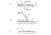
図2は、本発明の実施の形態1における配線基板の断面図である。図2において、2はセラミック基板であり、このセラミック基板2の上に導体ライン幅を10μm、ライン間隔を20μm、導体膜厚は焼成後で10μmにした第1導体パターン3を有し、またこの第1導体パターン3は径50μmのビア11を有している。この第1導体パターン3の上には絶縁層21を有し、更にその上には第2導体パターン4を有し、この第2導体パターン4はビア11と電気的に接続される。 FIG. 2 is a cross-sectional view of the wiring board according to
続いて、本実施の形態1における配線基板の製造方法を工程順に説明する。以下の説明に現れる各工程101〜116は、図1のブロック図に示されている。 Subsequently, the manufacturing method of the wiring board according to the first embodiment will be described in the order of steps. The steps 101 to 116 appearing in the following description are shown in the block diagram of FIG.
まず、図2において、第1導体パターン3およびビア11は凹版転写によってセラミック基板2に転写され形成される。 First, in FIG. 2, the
このとき図3に示すように、セラミック基板2上には転写に必要な接着層44を形成しなければならない。この接着層44を形成する接着層形成工程101に関して以下を説明する。 At this time, as shown in FIG. 3, an
まず、図4(a)の接着シート6を製造する接着シート形成工程102は、接着剤溶液製造工程103、塗工工程104、乾燥工程105から成る。 First, the adhesive
接着剤溶液製造工程103は、熱可塑性樹脂であるポリビニールブチラール樹脂粉末を有機溶剤中に投入し、攪拌装置を用いて十分に溶解させ接着剤溶液を製造する。このときポリビニールブチラール樹脂粉末(1)と有機溶剤(2)の重量比は、〔(1):(2)〕10:90〜30:70とした。これは有機溶剤が重量比90を超えると、乾燥性が悪くなったり凹版転写に必要な所望の膜厚が得られなくなり充分な接着強度が得られない為である。又、重量比70未満であると、溶解不良を起こしたり粘度が高くなり塗工性が悪くなる為である。よって、重量比は10:90〜30:70に制限することで溶液粘度も低く乾燥性も良好な接着剤溶液を得ることができた。特に好ましい範囲は(1):(2)の重量比が15:85である。 In the adhesive
有機溶剤としては、ポリビニールブチラール樹脂に溶解可能なものであれば特に限定されないが、例えばメタノール、エタノール、イソプロピルアルコール等のアルコール類、又は酢酸ブチル、酢酸エチル等のエステル類、又はトルエン、キシレン等の芳香族炭化水素類、又はアセトン、メチルエチルケトン等のケトン類等が挙げられる。これらは、単独あるいは2種以上が併用されてもよいが、混合溶剤として使用した方が接着剤粘度は低くなり、又貯蔵中の粘度変化も少なくなるなど好結果が得られる。これらの内、常圧での沸点が50〜130℃のものが、取り扱い性や揮発性の面から好ましい。本実施の形態では、溶剤コストも考慮しイソプロピルアルコールと酢酸ブチルを重量比50:50の混合溶剤として用いた。以上のような方法で、接着剤溶液を製造した。 The organic solvent is not particularly limited as long as it is soluble in polyvinyl butyral resin. For example, alcohols such as methanol, ethanol and isopropyl alcohol, esters such as butyl acetate and ethyl acetate, toluene, xylene and the like Aromatic hydrocarbons, or ketones such as acetone and methyl ethyl ketone. These may be used singly or in combination of two or more. However, when used as a mixed solvent, the adhesive viscosity is lowered, and good results are obtained such that the viscosity change during storage is reduced. Among these, those having a boiling point of 50 to 130 ° C. at normal pressure are preferable from the viewpoint of handleability and volatility. In the present embodiment, isopropyl alcohol and butyl acetate are used as a mixed solvent having a weight ratio of 50:50 in consideration of the solvent cost. The adhesive solution was manufactured by the method as described above.
次に、塗工工程104及び乾燥工程105として、上述の接着剤溶液をグラビアロール等による塗工装置を用いて、片面にシリコン離型処理が施された可とう性フィルム5の離型剤10側に形成し、その後乾燥させ接着剤中の有機溶剤分を除去し接着層44が形成された接着シート6を製造した。ここで、可とう性フィルム5としては厚みが38μmのポリエチレンテレフタレートを用いた。又、接着層44の厚みとしては、導体パターン幅や導体膜厚およびビアの有無によって1〜10μmの範囲で選択されるが、本実施の形態1では、厚みを6〜8μmにすることで導体パターンの変形や剥がれなどによる回路特性不良や、ビアの折れなどによる電気的接続不良が非常に少なく良好であった。 Next, as the
次に、貼り合わせ工程106として、図4(b)に示すように、接着層44が形成された接着シート6の接着層44側をセラミック基板2上に配置し、回転する熱ローラ15及び16が設けられたラミネーター装置にて貼り合わせた。ここで、貼り合わせ条件としては温度を150℃とした。これは接着層を形成するポリビニールブチラールの軟化点よりも約30℃程高い温度であり、ポリビニールブチラールを充分軟化させる為で、この温度の時にセラミック基板との密着性が良好であった。尚、下限値としては130℃でありそれ以下の温度では十分な密着強度が得られないことを確認した。又、圧力としては3kgf/cm2からセラミック基板の基板割れが発生しない限界圧力値までの範囲で設定することが望ましい。圧力値が上記下限値より小さいと、セラミック基板にうねりがある場合などに接着シートとセラミック基板との間が完全に密着せず両者の間に気泡が混入したり、また十分な密着強度が得られなかった。本実施の形態では、圧力を5kgf/cm2とし送り速度としては0.6m/分とすることで貼り合わせ時の基板割れ及びシワや気泡等のない良好な貼り合わせができた。Next, as the
次に、剥離工程107として、図4(c)に示すように、貼り合わせた接着シート6の可とう性フィルム5を離型剤10とともに剥離して取り除いた。以上のような方法で、セラミック基板2上に接着層44を形成した。 Next, as shown in FIG. 4C, as the peeling
なお、本実施の形態1において、図4(d)に示すようにセラミック基板2の裏表両面同時に接着層44を設けてもよく、その結果、凹版転写による導体パターン形成も両面に形成できる。 In the first embodiment, as shown in FIG. 4 (d), the
またさらに、図5に示すように、凹版転写時におけるカメラ認識での位置合わせ基準用として設けられたセラミック基板2の微小な貫通孔14を塞がないような大きさの接着シート6を貼り合わせてもよく、その結果、従来のセラミック基板全面を浸漬させディップする方法のように貫通孔14に入り込んでしまった接着剤を除去する必要がなくなる。 Further, as shown in FIG. 5, an
一方、図2において、第1導体パターン3およびビア11は凹版による転写によって形成される。 On the other hand, in FIG. 2, the
この第1導体パターン3およびビア11の形成方法として、図6および図7を参照しながら、ペーストパターン製造工程108を説明する。 As a method for forming the
まず、凹版製造工程109としては、使用する凹版40は材料として厚さ125μmの可とう性樹脂基材であるポリイミドフィルムを用いた。そして、エキシマレーザ装置を用いて、紫外線領域の波長248nmのレーザビームをこのポリイミドフィルムに照射し、所望の導体パターンに対応した形状の第1の溝12を形成した。すなわち、レーザビームで照射されたポリイミドは光化学反応で分解されるため第1導体パターン3(図2に示す)に相当する第1の溝12がポリイミドフィルムに形成される。次に、第1導体パターン3のビア11(図2に示す)に対応する第2の溝13をエキシマレーザ装置を用いて形成した。 First, as the
なお、上述の凹版40の材料として用いる可とう性樹脂基材としては、溝12および溝13を形成する方法としてエキシマレーザを用いる場合は、光化学反応で分解される材料であれば特に限定されず、ポリイミドの他に例えばポリエチレンテレフタレートや、ポリエーテルイミド、アラミドなども使用できる。しかしここで、凹版40の溝12および溝13がファインパターンになるにつれて以下の問題が生ずる。すなわち、図6に示すように溝12および溝13に導電性ペースト42を充填するのにスキージ41を用いるが、その摺動により凹版40の表面の磨耗、及び上記溝12および溝13の変形が発生し、配線基板としての信頼性が低下する。本実施の形態では、弾性率930kg/cm2のポリイミドフィルムと弾性率1500kg/cm2のアラミドフィルムを用いることで100回使用しても溝の変形はない。ここで、溝12および溝13の中に充填されて転写される導電性ペースト42と凹版40との剥離性を高めることを目的として凹版40の表面、特に溝12および溝13の表面に剥離層(図示せず)を形成した。剥離層はフッ化炭素系単分子膜を使用した。以上のような方法で、凹版40を製造した。In addition, as a flexible resin base material used as a material of the above-mentioned
次に、充填工程110として、剥離層が形成された凹版40の表面に、導電性ペースト42を塗布する。ここで、導電性ペーストとしてはAgペーストを用いた。そして、塗布後の凹版40の表面をスキージ41で掻くことによって、凹版40表面の余分なAgペーストを除去するとともに、溝12および溝13の中にAgペーストを充分に充填した。 Next, as the filling
次に、乾燥工程111として、充填されたAgペーストは凹版40とともに乾燥機を用いて乾燥させて、Agペースト中の有機溶剤を蒸発させる。そのため、有機溶剤の蒸発分に相当するだけ、溝12および溝13の内部に充填されているAgペーストの体積が減少する。そこで、この体積減少分を補うために、Agペーストの充填工程110および乾燥工程111を再度繰り返す。この繰り返しによって充填されているAgペーストの乾燥後の厚さを溝12および溝13の深さとほぼ同等にすることができる。 Next, as the drying step 111, the filled Ag paste is dried together with the
次に、プレス工程112として、図7(a)に示すように、凹版40の溝12および溝13の形成面と、接着層形成工程101で形成した接着層44の形成面とを対向させた状態で貼り合わせ、プレス装置などを用いて加熱・加圧して貼り合わせる。なお、このプレス工程の温度は150℃とした。これは接着層44を形成する熱可塑性樹脂であるポリビニールブチラールの軟化点よりも約30℃程高い温度であり、このときの導体パターンの転写性が良好であることを確認した。 Next, as shown in FIG. 7A, as the
次に、転写工程113として、図7(b)に示すように、貼り合わせられた凹版40とセラミック基板2の温度を常温まで下げてから凹版40をセラミック基板2から剥離し、乾燥済み導体ペースト43の転写を行う。このとき凹版40はフレキシブル性に富んでいるため、凹版40を90°以上の角度に曲げることが可能である。その結果、凹版40を容易に剥離することができる。 Next, as shown in FIG. 7B, as the
次に、焼成工程114として、乾燥済み導体ペースト43が転写されたセラミック基板2をピーク温度850℃の温度プロファイルの下で焼成する。焼成の対象になるセラミック基板2は接着層44を介して導体パターンが形成されているので、焼成条件の設定によっては接着層44から燃焼ガスが勢い良く発生して、導体パターンの不良の原因となる変形や剥がれが生じることがある。そのような不具合の発生を防ぐためには、接着層44の燃焼が開始されてから終了するまでの温度に相当する200℃〜500℃の間の昇温時の温度勾配を200℃/Hr以下にすることが望ましい。 Next, as the
以上の工程により、第1導体パターン3およびビア11が形成され、最小ライン幅10μm、最小ライン間隔20μm、焼成後の導体膜厚10μm、ビア径50μm、ビア高さ60μmの図7(c)に示すものが得られた。溝12および溝13の寸法よりも小さくなったのは、導体材料が焼成によって収縮したからである。 Through the above steps, the
次に、絶縁層形成工程115として、図8(a)に示すように、第1導体パターン3およびビア11の形成されたセラミック基板2の上に絶縁ペーストをスクリーン印刷法により印刷した。続いてこの絶縁ペーストを乾燥し、焼成することによって絶縁層21を形成した。 Next, as an insulating
次に、第2導体パターン形成工程116として、図8(b)に示すように、絶縁層21の上にスクリーン印刷法によって導体ペーストを印刷した。続いてこの導体ペーストを乾燥し焼成することによって第2導体パターン4を形成した。ここで、第2導体パターン4と第1導体パターン3はビア11を介して電気的に接続される。 Next, as a second conductor
以上の製造方法により、予め可とう性フィルム5の表面に剥離剤10を介して略均一な厚みの接着層44が形成された接着シート6とセラミック基板2とを貼り合わせて加熱・圧着することで、接着シート6をセラミック基板2へ接着し、可とう性フィルム5を剥離することで接着層44を形成させるので、第1導体パターン3およびビア11の接着に必要な均一かつ安定した膜厚の接着層44を得ることができる。従って、焼成工程114において、接着層44自身の燃焼と収縮力は小さくでき、接着層44上に形成された第1導体パターン3およびビア11の流動が小さくなり、第1導体パターン3およびビア11の変形や剥がれの発生の少ない配線基板が得られる。 By the above manufacturing method, the
(実施の形態2)
本実施の形態2および図9により請求項2に記載の発明を説明する。(Embodiment 2)
The second embodiment and FIG. 9 will explain the invention described in
図9は、本実施の形態2における配線基板の製造工程を示す断面図である。図9(a)〜(c)に示すように、セラミック基板2に熱可塑性樹脂からなる接着層44を形成する接着層形成工程101までは、実施の形態1の記載方法と同様とした。 FIG. 9 is a cross-sectional view showing the manufacturing process of the wiring board according to the second embodiment. As shown in FIGS. 9A to 9C, the process up to the adhesive layer forming step 101 for forming the
次に、図9(d)に示すように、セラミック基板2の接着層44形成面の上にスクリーン印刷法により第1導体パターン3を形成した。 Next, as shown in FIG. 9D, the
次に、図9(e)に示すように、第1導体パターン3の乾燥を行い、焼成した。 Next, as shown in FIG. 9E, the
本実施の形態2が実施の形態1と異なる点は、ペーストパターン製造工程108を凹版転写法ではなくスクリーン印刷法で行う点であり、凹版転写法より容易に生産性の高いパターン形成が可能である。更に、接着層44を形成するポリビニールブチラール樹脂が導電性ペースト内の溶剤成分を吸収することで、にじみやダレを抑制することができる。従って、凹版転写法より生産性の高いスクリーン印刷で、隣接するパターンのショートが少ない配線基板が得られる。 The second embodiment is different from the first embodiment in that the paste
(実施の形態3)
本実施の形態3および図10により請求項4に記載の発明を説明する。(Embodiment 3)
The invention described in
図10は本実施の形態3における配線基板の製造工程を示す断面図である。図10(a)および(b)に示すように、接着シート6を形成する接着シート形成工程102と乾燥済み導電性ペースト43を凹版40に形成する乾燥工程111までは、実施の形態1の記載方法と同様とした。 FIG. 10 is a cross-sectional view showing the manufacturing process of the wiring board according to the third embodiment. As shown in FIGS. 10A and 10B, the description up to the first embodiment includes the adhesive
次に、貼り合わせ工程106として、図10(c)に示すように、接着シート6の接着層44形成面と凹版40の乾燥済み導電性ペースト43形成面を対向するように配置し、回転する熱ローラ15および16が設けられたラミネーター装置にて貼り合わせた。ここで、貼り合わせ条件としては温度を150℃とした。これは接着層を形成するポリビニールブチラールの軟化点よりも約30℃程高い温度であり、ポリビニールブチラールを充分軟化させるためで、この温度の時に凹版との密着性が良好であった。尚、下限値としては130℃でありそれ以下の温度では十分な密着強度が得られないことを確認した。又、圧力としては3kgf/cm2から10kgf/cm2までの範囲で設定することが望ましい。圧力値が上記下限値より小さいと、接着シートと凹版との間が完全に密着せず両者の間に気泡が混入したり、また十分な密着強度が得られなかった。本実施の形態では、圧力を5kgf/cm2とし送り速度としては0.6m/分とすることで貼り合わせ時のシワや気泡等のない良好な貼り合わせができた。Next, as shown in FIG. 10 (c), as the
次に、剥離工程107として、図10(d)に示すように、貼り合わせた接着シート6は可とう性フィルム5を離型剤10とともに剥離して取り除き、接着層44を形成した。 Next, as shown in FIG. 10 (d), as the peeling
次に、プレス工程112として、図10(e)に示すように、セラミック基板2上に凹版40の接着層44形成面を配置させプレス装置などを用いて加熱・加圧して貼り合わせる。なお、このプレス工程の温度は150℃とした。これは接着層44を形成する熱可塑性樹脂であるポリビニールブチラールの軟化点よりも約30℃程高い温度であり、この時の導体パターンの転写性が良好であることを確認した。 Next, as a
次に、図10(f)に示すように、貼り合わせられた凹版40とセラミック基板2の温度を常温まで下げてから凹版40をセラミック基板2から剥離させ、第1導体パターン3に対応する乾燥済み導体ペースト43の転写を行う転写工程113以降は実施の形態1と同様とした。 Next, as shown in FIG. 10 (f), the temperature of the bonded
本実施の形態3が実施の形態1と異なる点は、接着シート6の接着層44をセラミック基板2ではなく凹版40に形成する点であり、以下に示す効果を有する。 The third embodiment is different from the first embodiment in that the
すなわち、導電性ペーストを充填・乾燥した凹版40の表面に接着シート6を貼り合わせることで、形成した乾燥済み導体ペースト43の破損、又は埃や異物などから保護する機能も果たし、パターンのショートやオープンといった回路特性不良も少なく信頼性の高い配線基板を得ることができる。 That is, by bonding the
(実施の形態4)
本実施の形態4および図11により請求項8に記載の発明を説明する。(Embodiment 4)
The invention according to claim 8 will be described with reference to the fourth embodiment and FIG.
図11は本実施の形態4における配線基板の製造工程を示す断面図である。まず、接着層44を形成する接着剤溶液の製造工程103は、実施の形態1と同様とした。 FIG. 11 is a cross-sectional view showing the manufacturing process of the wiring board according to the fourth embodiment. First, the
図11(a)に示すように、接着シート6を形成する接着シート形成工程102は、巻き出しローラ50から繰り出された可とう性フィルム5の離型剤10側に実施の形態1と同様にして、グラビアロールコーターを用いて接着剤溶液を連続的に塗工、乾燥を行い巻き取りローラ51にロール状に巻き取って回収した。 As shown in FIG. 11A, the adhesive
次に、貼り合わせ工程106として、図11(b)に示すように、第2巻き出しローラ52から繰り出された接着シート6の接着層44形成面上にセラミック基板2を配置し、回転する熱ローラ15及び16が設けられたラミネーター装置にて連続的に貼り合わせて回収した。ここで、貼り合わせ条件としては、実施の形態1と同様とした。 Next, as the
このとき、図11(c)に示すように、セラミック基板2の裏表両面同時に接着層44を設けてもよく、その結果、凹版転写による導体パターン形成も両面に形成できる。 At this time, as shown in FIG. 11C, the
次に、剥離工程107として、図11(d)に示すように、セラミック基板2の端面に沿って接着シート6を切断加工し、その後貼り合わせた接着シート6の可とう性フィルム5を離型剤10とともに剥離して取り除き、セラミック基板2上に接着層44を形成した。 Next, as shown in FIG. 11 (d), as the peeling
次に、図11(e)に示すように、ペーストパターン製造工程108以降は実施の形態1と同様とした。 Next, as shown in FIG. 11E, the paste
本実施の形態4が実施の形態1と異なる点は、可とう性フィルム5が連続したシート形状となっている点であり、以下に示す効果を有する。 The fourth embodiment is different from the first embodiment in that the
すなわち、可とう性フィルム5を連続したシート形状にすることで接着シート6の形成やセラミック基板2への貼り合わせなどで連続生産が可能となり生産効率も上がる。 That is, by making the
また、巻き取った1ロールをロット単位として扱えることで間違いも少なくなり、効率的で信頼性の高い配線基板を得ることができる。 Further, since one wound roll can be handled as a lot unit, errors are reduced, and an efficient and highly reliable wiring board can be obtained.
(実施の形態5)
本実施の形態5および図12により請求項9に記載の発明を説明する。(Embodiment 5)
The invention described in
図12は本実施の形態5における配線基板の製造工程を示す断面図である。まず、図12(a)〜(c)に示すように、接着シート6をセラミック基板2上に形成する貼り合わせ工程106と乾燥済み導電性ペースト43を凹版40に形成する乾燥工程111までは、実施の形態1と同様とした。 FIG. 12 is a cross-sectional view showing the manufacturing process of the wiring board according to the fifth embodiment. First, as shown in FIGS. 12A to 12C, the
次に、剥離工程107として、図12(d)に示すように、セラミック基板2に貼り合わせた接着シート6は可とう性フィルム5を離型剤10とともに剥離して取り除き、セラミック基板2上に接着層44を形成した。 Next, as a peeling
次に、プレス工程112として、図12(e)に示すように、この凹版40の溝12および溝13の形成面と、セラミック基板2の接着層44の形成面とを対向させプレス装置などを用いて加熱・加圧して貼り合わせる。 Next, as a
このとき、セラミック基板2に貼り合わせた接着シート6の可とう性フィルム5を剥離して取り除く剥離工程107は、プレス工程112の直前に行った。 At this time, the
次に、図12(f)に示すように、貼り合わせられた凹版40とセラミック基板2の温度を常温まで下げてから凹版40をセラミック基板2から剥離させ、乾燥済み導体ペースト43の転写を行う転写工程113以降は実施の形態1と同様とした。 Next, as shown in FIG. 12 (f), the temperature of the bonded
本実施の形態5が実施の形態1と異なる点は、可とう性フィルム5を剥離し接着層44を形成する工程は、凹版40とセラミック基板2を貼り合わせる直前に行う点であり、以下に示す効果を有する。 The fifth embodiment is different from the first embodiment in that the step of peeling the
すなわち、可とう性フィルム5を凹版40とセラミック基板2を貼り合わせる直前まで残すことで、接着層44に対して保護層として機能することができ、工程の移動間に埃や異物が付着したり、傷が付くということが防止できるので、基板同士を積み重ねて保管することもでき、保管スペースが小さくできる。 That is, by leaving the
また、可とう性フィルム5が接着層44を保護するので、素手で扱っても接着層44に皮脂などが付着することがないため、基板の取り扱いも容易になるなど効率的で信頼性の高い配線基板を得ることができる。 Further, since the
(実施の形態6)
本実施の形態6および図13により請求項10に記載の発明を説明する。(Embodiment 6)
The invention described in
図13は本実施の形態6における配線基板の製造方法の流れを示すブロック図である。なお、図13において、図1と同じ工程は同一番号とし、その説明は、省略している。 FIG. 13 is a block diagram showing a flow of a method of manufacturing a wiring board according to the sixth embodiment. In FIG. 13, the same steps as those in FIG. 1 are denoted by the same reference numerals, and the description thereof is omitted.
本実施の形態では、実施の形態1に対し、溶融工程301が異なっており、この工程について詳細に説明する。剥離工程107のあと、溶融工程301として、乾燥機などを用いて、接着層を形成するポリビニールブチラールを溶融させた。ここで、溶融条件としては、溶融温度を180℃とした。これは、熱可塑性樹脂であるポリビニールブチラールの軟化点よりも約60℃程高い温度であり、軟化後更に流動性の高い状態になることで、セラミック基板表面の結晶粒子間に入り込みやすくする為である。又、溶融時間としては、10分から30分とした。 In the present embodiment, the
以上の製造方法により、接着層を形成する熱可塑性樹脂であるポリビニールブチラールを溶融することで、セラミック基板表面の粒子間に入り込み凹凸がなくなる。従って、圧力を加えても応力集中が少なくなる為、プレス工程において基板割れの少ない配線基板が得られる。なお、これは特にフォルステライトなど多孔質な基板において非常に効果的である。 By melting the polyvinyl butyral, which is a thermoplastic resin forming the adhesive layer, by the above manufacturing method, it enters between the particles on the surface of the ceramic substrate and the unevenness is eliminated. Therefore, even if pressure is applied, the stress concentration is reduced, so that a wiring board with less substrate cracking can be obtained in the pressing process. This is particularly effective for porous substrates such as forsterite.
本発明にかかる配線基板の製造方法は、導体パターンの変形や剥がれの発生の少ない配線基板を得ることができるという効果を有し、特にセラミック基板などへの導体パターンの形成に対して利用すると有用である。 The method for manufacturing a wiring board according to the present invention has an effect that a wiring board with less deformation and peeling of the conductor pattern can be obtained, and is particularly useful when used for forming a conductor pattern on a ceramic substrate or the like. It is.
2 セラミック基板
3 第1導体パターン
5 可とう性フィルム
6 接着シート
10 離型剤
42 導電性ペースト
44 接着層
101 接着層形成工程
106 貼り合わせ工程
107 剥離工程
108 ペーストパターン製造工程
114 焼成工程2
Claims (10)
Translated fromJapanesePriority Applications (1)
| Application Number | Priority Date | Filing Date | Title |
|---|---|---|---|
| JP2005038814AJP2005277394A (en) | 2004-02-23 | 2005-02-16 | Wiring board manufacturing method |
Applications Claiming Priority (2)
| Application Number | Priority Date | Filing Date | Title |
|---|---|---|---|
| JP2004045892 | 2004-02-23 | ||
| JP2005038814AJP2005277394A (en) | 2004-02-23 | 2005-02-16 | Wiring board manufacturing method |
Publications (1)
| Publication Number | Publication Date |
|---|---|
| JP2005277394Atrue JP2005277394A (en) | 2005-10-06 |
Family
ID=35176660
Family Applications (1)
| Application Number | Title | Priority Date | Filing Date |
|---|---|---|---|
| JP2005038814APendingJP2005277394A (en) | 2004-02-23 | 2005-02-16 | Wiring board manufacturing method |
Country Status (1)
| Country | Link |
|---|---|
| JP (1) | JP2005277394A (en) |
Cited By (1)
| Publication number | Priority date | Publication date | Assignee | Title |
|---|---|---|---|---|
| KR20160102166A (en)* | 2013-11-01 | 2016-08-29 | 피피지 인더스트리즈 오하이오 인코포레이티드 | Methods of transferring electrically conductive materials |
- 2005
- 2005-02-16JPJP2005038814Apatent/JP2005277394A/enactivePending
Cited By (5)
| Publication number | Priority date | Publication date | Assignee | Title |
|---|---|---|---|---|
| KR20160102166A (en)* | 2013-11-01 | 2016-08-29 | 피피지 인더스트리즈 오하이오 인코포레이티드 | Methods of transferring electrically conductive materials |
| JP2016536810A (en)* | 2013-11-01 | 2016-11-24 | ピーピージー・インダストリーズ・オハイオ・インコーポレイテッドPPG Industries Ohio,Inc. | Method for transferring conductive material |
| CN106538075A (en)* | 2013-11-01 | 2017-03-22 | Ppg工业俄亥俄公司 | Methods of transferring electrically conductive materials |
| US10219388B2 (en) | 2013-11-01 | 2019-02-26 | Ppg Industries Ohio, Inc. | Methods of transferring electrically conductive materials |
| KR102045113B1 (en) | 2013-11-01 | 2019-11-14 | 피피지 인더스트리즈 오하이오 인코포레이티드 | Methods of transferring electrically conductive materials |
Similar Documents
| Publication | Publication Date | Title |
|---|---|---|
| JP3173439B2 (en) | Ceramic multilayer substrate and method of manufacturing the same | |
| KR101044103B1 (en) | Multilayer printed circuit board and its manufacturing method | |
| JP2004146694A (en) | Method for manufacturing multilayer circuit board and multilayer circuit board using the same | |
| JP2003318545A (en) | Multilayer printed wiring board and its manufacturing method | |
| JP3132493B2 (en) | Wiring board manufacturing method and conductor paste used therefor | |
| WO2000035260A1 (en) | Method of manufacturing ceramic substrate | |
| JP3670487B2 (en) | Wiring board manufacturing method | |
| JP2004253432A (en) | Manufacturing method of printed wiring board | |
| JPH07169635A (en) | Electronic component and manufacturing method thereof | |
| US7186307B2 (en) | Method for manufacturing a ceramic multilayer circuit board | |
| JP2004055777A (en) | Method for manufacturing composite multilayer wiring board | |
| JP2007227881A (en) | Composite wiring board, and method of manufacturing same | |
| JP2005277394A (en) | Wiring board manufacturing method | |
| JP2005353420A (en) | Conductive material, conductive material-carrying sheet, conductive material filling method and apparatus | |
| JP2011096754A (en) | Support film, method of manufacturing wiring substrate using the same, and wiring substrate | |
| JP2616572B2 (en) | Method for manufacturing multilayer printed wiring board | |
| JP2004207510A (en) | Multilayered circuit board and manufacturing method thereof | |
| JP3823457B2 (en) | Manufacturing method of ceramic wiring board | |
| JPH07122839A (en) | Method for manufacturing ceramic wiring board | |
| JP5409334B2 (en) | Wiring board manufacturing method | |
| JP3709453B2 (en) | Manufacturing method of ceramic multilayer wiring board | |
| JP4721742B2 (en) | Manufacturing method of electronic parts | |
| JP2003008226A (en) | Method of manufacturing printed substrate | |
| JP5451365B2 (en) | Wiring board manufacturing method | |
| JP2009094330A (en) | Wiring board base material and method for manufacturing wiring board base material |