JP2005276689A - Manufacturing method for organic electroluminescent element, forming method for electrode or wiring containing conductive oxide film, manufacturing method for electronic apparatus, organic electroluminescent element, and electronic apparatus - Google Patents
Manufacturing method for organic electroluminescent element, forming method for electrode or wiring containing conductive oxide film, manufacturing method for electronic apparatus, organic electroluminescent element, and electronic apparatusDownload PDFInfo
- Publication number
- JP2005276689A JP2005276689AJP2004089729AJP2004089729AJP2005276689AJP 2005276689 AJP2005276689 AJP 2005276689AJP 2004089729 AJP2004089729 AJP 2004089729AJP 2004089729 AJP2004089729 AJP 2004089729AJP 2005276689 AJP2005276689 AJP 2005276689A
- Authority
- JP
- Japan
- Prior art keywords
- film
- metal
- electrode
- forming
- manufacturing
- Prior art date
- Legal status (The legal status is an assumption and is not a legal conclusion. Google has not performed a legal analysis and makes no representation as to the accuracy of the status listed.)
- Granted
Links
- 238000000034methodMethods0.000titleclaimsabstractdescription106
- 238000004519manufacturing processMethods0.000titleclaimsdescription53
- 238000007254oxidation reactionMethods0.000claimsabstractdescription72
- 230000003647oxidationEffects0.000claimsabstractdescription69
- 239000011368organic materialSubstances0.000claimsabstractdescription57
- 239000004020conductorSubstances0.000claimsabstractdescription49
- -1oxygen radical ionsChemical class0.000claimsabstractdescription33
- 239000001301oxygenSubstances0.000claimsabstractdescription32
- 229910052760oxygenInorganic materials0.000claimsabstractdescription32
- 230000015572biosynthetic processEffects0.000claimsabstractdescription18
- 238000005546reactive sputteringMethods0.000claimsabstractdescription15
- 238000006243chemical reactionMethods0.000claimsabstractdescription10
- 238000010030laminatingMethods0.000claimsabstractdescription5
- 229910052751metalInorganic materials0.000claimsdescription105
- 239000002184metalSubstances0.000claimsdescription105
- 239000000463materialSubstances0.000claimsdescription96
- 239000010410layerSubstances0.000claimsdescription56
- 239000000956alloySubstances0.000claimsdescription53
- 229910044991metal oxideInorganic materials0.000claimsdescription49
- 150000004706metal oxidesChemical class0.000claimsdescription49
- 229910001092metal group alloyInorganic materials0.000claimsdescription41
- 150000004767nitridesChemical class0.000claimsdescription38
- 239000007769metal materialSubstances0.000claimsdescription28
- 238000004544sputter depositionMethods0.000claimsdescription26
- 238000005401electroluminescenceMethods0.000claimsdescription25
- 239000000758substrateSubstances0.000claimsdescription21
- 230000001681protective effectEffects0.000claimsdescription17
- 150000002500ionsChemical class0.000claimsdescription11
- 239000004065semiconductorSubstances0.000claimsdescription10
- 229910000808amorphous metal alloyInorganic materials0.000claimsdescription8
- 229910045601alloyInorganic materials0.000claimsdescription7
- 239000007789gasSubstances0.000claimsdescription7
- 229910052738indiumInorganic materials0.000claimsdescription7
- 239000004973liquid crystal related substanceSubstances0.000claimsdescription7
- 230000001590oxidative effectEffects0.000claimsdescription7
- 229910052718tinInorganic materials0.000claimsdescription7
- 238000000151depositionMethods0.000claimsdescription6
- KJTLSVCANCCWHF-UHFFFAOYSA-NRutheniumChemical compound[Ru]KJTLSVCANCCWHF-UHFFFAOYSA-N0.000claimsdescription4
- ATJFFYVFTNAWJD-UHFFFAOYSA-NTinChemical compound[Sn]ATJFFYVFTNAWJD-UHFFFAOYSA-N0.000claimsdescription4
- HCHKCACWOHOZIP-UHFFFAOYSA-NZincChemical compound[Zn]HCHKCACWOHOZIP-UHFFFAOYSA-N0.000claimsdescription4
- 229910052784alkaline earth metalInorganic materials0.000claimsdescription4
- 150000001342alkaline earth metalsChemical class0.000claimsdescription4
- 229910052782aluminiumInorganic materials0.000claimsdescription4
- XAGFODPZIPBFFR-UHFFFAOYSA-NaluminiumChemical compound[Al]XAGFODPZIPBFFR-UHFFFAOYSA-N0.000claimsdescription4
- APFVFJFRJDLVQX-UHFFFAOYSA-Nindium atomChemical compound[In]APFVFJFRJDLVQX-UHFFFAOYSA-N0.000claimsdescription4
- 239000011261inert gasSubstances0.000claimsdescription4
- 229910052741iridiumInorganic materials0.000claimsdescription4
- GKOZUEZYRPOHIO-UHFFFAOYSA-Niridium atomChemical compound[Ir]GKOZUEZYRPOHIO-UHFFFAOYSA-N0.000claimsdescription4
- 229910052761rare earth metalInorganic materials0.000claimsdescription4
- 150000002910rare earth metalsChemical class0.000claimsdescription4
- 229910052707rutheniumInorganic materials0.000claimsdescription4
- 229910052725zincInorganic materials0.000claimsdescription4
- 239000011701zincSubstances0.000claimsdescription4
- 150000003254radicalsChemical class0.000claimsdescription2
- 239000002356single layerSubstances0.000claimsdescription2
- 230000006378damageEffects0.000abstractdescription24
- 239000007772electrode materialSubstances0.000abstractdescription17
- 230000002950deficientEffects0.000abstract2
- IJGRMHOSHXDMSA-UHFFFAOYSA-NAtomic nitrogenChemical compoundN#NIJGRMHOSHXDMSA-UHFFFAOYSA-N0.000description22
- 229910052757nitrogenInorganic materials0.000description11
- 230000007547defectEffects0.000description6
- 230000008021depositionEffects0.000description5
- 239000012528membraneSubstances0.000description4
- 239000002344surface layerSubstances0.000description4
- XKRFYHLGVUSROY-UHFFFAOYSA-NArgonChemical compound[Ar]XKRFYHLGVUSROY-UHFFFAOYSA-N0.000description3
- MYMOFIZGZYHOMD-UHFFFAOYSA-NDioxygenChemical compoundO=OMYMOFIZGZYHOMD-UHFFFAOYSA-N0.000description3
- 238000004140cleaningMethods0.000description3
- 229910001882dioxygenInorganic materials0.000description3
- 230000005284excitationEffects0.000description3
- 238000002347injectionMethods0.000description3
- 239000007924injectionSubstances0.000description3
- 238000002834transmittanceMethods0.000description3
- 229910006404SnO 2Inorganic materials0.000description2
- 229910052786argonInorganic materials0.000description2
- QVGXLLKOCUKJST-UHFFFAOYSA-Natomic oxygenChemical compound[O]QVGXLLKOCUKJST-UHFFFAOYSA-N0.000description2
- 230000005540biological transmissionEffects0.000description2
- 239000000470constituentSubstances0.000description2
- 230000000694effectsEffects0.000description2
- 238000010438heat treatmentMethods0.000description2
- 230000005525hole transportEffects0.000description2
- 239000000203mixtureSubstances0.000description2
- 230000006798recombinationEffects0.000description2
- 238000005215recombinationMethods0.000description2
- 239000000126substanceSubstances0.000description2
- 229910018072Al 2 O 3Inorganic materials0.000description1
- 230000015556catabolic processEffects0.000description1
- 239000007795chemical reaction productSubstances0.000description1
- 230000003749cleanlinessEffects0.000description1
- 150000001875compoundsChemical class0.000description1
- 238000004320controlled atmosphereMethods0.000description1
- 238000002425crystallisationMethods0.000description1
- 230000008025crystallizationEffects0.000description1
- 238000006731degradation reactionMethods0.000description1
- 230000006866deteriorationEffects0.000description1
- 238000010894electron beam technologyMethods0.000description1
- 239000012535impuritySubstances0.000description1
- 238000004020luminiscence typeMethods0.000description1
- 239000011159matrix materialSubstances0.000description1
- 229910000480nickel oxideInorganic materials0.000description1
- 230000004792oxidative damageEffects0.000description1
- 238000010525oxidative degradation reactionMethods0.000description1
- GNRSAWUEBMWBQH-UHFFFAOYSA-NoxonickelChemical compound[Ni]=OGNRSAWUEBMWBQH-UHFFFAOYSA-N0.000description1
- 150000002926oxygenChemical class0.000description1
- 229920000642polymerPolymers0.000description1
- 230000001737promoting effectEffects0.000description1
- 239000000243solutionSubstances0.000description1
- 230000007847structural defectEffects0.000description1
- 239000013077target materialSubstances0.000description1
- 230000008646thermal stressEffects0.000description1
Images


Classifications
- Y—GENERAL TAGGING OF NEW TECHNOLOGICAL DEVELOPMENTS; GENERAL TAGGING OF CROSS-SECTIONAL TECHNOLOGIES SPANNING OVER SEVERAL SECTIONS OF THE IPC; TECHNICAL SUBJECTS COVERED BY FORMER USPC CROSS-REFERENCE ART COLLECTIONS [XRACs] AND DIGESTS
- Y02—TECHNOLOGIES OR APPLICATIONS FOR MITIGATION OR ADAPTATION AGAINST CLIMATE CHANGE
- Y02E—REDUCTION OF GREENHOUSE GAS [GHG] EMISSIONS, RELATED TO ENERGY GENERATION, TRANSMISSION OR DISTRIBUTION
- Y02E10/00—Energy generation through renewable energy sources
- Y02E10/50—Photovoltaic [PV] energy
Landscapes
- Electroluminescent Light Sources (AREA)
- Manufacturing Of Printed Circuit Boards (AREA)
- Photovoltaic Devices (AREA)
- Manufacturing Of Electric Cables (AREA)
- Physical Vapour Deposition (AREA)
Abstract
Description
Translated fromJapanese本発明は導電酸化物膜を含む電極または配線の形成方法に関し、また導電酸化物膜を含む電極または配線を備えた有機エレクトロルミネッセンス素子およびその他電子装置の製造方法に関する。 The present invention relates to a method for forming an electrode or a wiring including a conductive oxide film, and also relates to a method for manufacturing an organic electroluminescence element including an electrode or a wiring including a conductive oxide film and other electronic devices.
電子装置には導電酸化物膜(多くの場合実質的に透明である)を含む電極または配線を備えたものがある。有機エレクトロルミネッセンス素子はその一例である。有機エレクトロルミネッセンス素子は互いに対向する2つの電極間に、発光層を含む有機材料膜を設けた構成を備え、両電極間に電圧を印加することにより、有機物材料膜中の発光層に電子及びホールを注入して、電子とホールの再結合により発光を行なっている。従来、この種の有機エレクトロルミネッセンス素子には、透明な基盤上に、透明な電極を形成しておき、発光層から発光を基盤側から取り出す形式のものと、基盤の電極上に形成された有機物材料膜上に透明電極を設け、透明電極から発光層からの発光を取り出す形式のトップエミッション型有機エレクトロルミネッセンス素子があり、ここでは、トップエミッション型有機エレクトロルミネッセンス素子に限って説明する。 Some electronic devices have electrodes or wiring that include a conductive oxide film (often substantially transparent). An organic electroluminescence element is an example. The organic electroluminescence device has a configuration in which an organic material film including a light emitting layer is provided between two electrodes facing each other, and a voltage is applied between the two electrodes, whereby electrons and holes are formed in the light emitting layer in the organic material film. To emit light by recombination of electrons and holes. Conventionally, in this type of organic electroluminescence device, a transparent electrode is formed on a transparent substrate, and light emitted from the light emitting layer is extracted from the substrate side, and an organic material formed on the substrate electrode There is a top emission type organic electroluminescence element in which a transparent electrode is provided on a material film and light emission from the light emitting layer is extracted from the transparent electrode. Here, only the top emission type organic electroluminescence element will be described.
光の透過性を有する導電性透明電極膜には、ITO(In2O3-SnO2)、IZO(In2O3-ZnO)、AZO(ZnO-Al2O3),SnO2などの金属酸化膜材料がある。例えば、ITOなどは、LCDや有機EL素子(以下:OLED)などのフラットパネルディスプレーに広く用いられている。また透明でない導電性酸化物膜の電極または配線は、仕事関数の調整や密着性の向上などの目的で各種電子装置に用いられている。このような導電性酸化物膜を反応性スパッタリング法などで成膜する方法は、生産性、膜質(導電性、光透過性、表面平坦性)の点で優れているため広く用いられている。Conductive transparent electrode films with light transmission properties include metal oxides such as ITO (In2 O3 —SnO2 ), IZO (In2 O3 —ZnO), AZO (ZnO—Al2 O3 ), and SnO2. There is a membrane material. For example, ITO is widely used for flat panel displays such as LCDs and organic EL elements (hereinafter referred to as OLEDs). Non-transparent conductive oxide film electrodes or wirings are used in various electronic devices for the purpose of adjusting work function and improving adhesion. A method for forming such a conductive oxide film by a reactive sputtering method or the like is widely used because it is excellent in terms of productivity and film quality (conductivity, light transmittance, and surface flatness).
図1(a)及び(b)を参照して、従来のトップエミッション型有機エレクトロルミネッセンス素子の素子構成、並びに、プロセス工程をそれぞれ説明する。図1(a)及び(b)に示されたように、この形式の有機エレクトロルミネッセンス素子は、非透明な基盤10を洗浄した後、当該基盤10の表面に、第1の金属電極(陰極)12を形成する。続いて、第1の金属電極12上に、発光層を含む有機物材料膜14(通常は正孔注入層、正孔輸送層、発光層、電子輸送層を含む)が形成され、当該有機物材料膜14上には、陽極を構成する透明な第2の電極16が設けられている。図1(a)に示されているように、第2の電極16と第1の電極12との間に、電圧を印加することにより、発光層14からの発光は第2の電極16側から出射される。 With reference to FIG. 1 (a) and (b), the element structure of the conventional top emission type organic electroluminescent element and a process process are each demonstrated. As shown in FIGS. 1 (a) and 1 (b), this type of organic electroluminescent element is formed by cleaning a
ここで、金属酸化膜を成膜して透明な第2の電極16を形成する場合、前述したように、反応性スパッタリング法が用いられることが多い。 Here, when forming the transparent
更に、特開2003−77651(特許文献1)には、この種のトップエミッション型有機エレクトロルミネッセンス素子の製造において、透明な第2の電極の成膜の際、有機物材料膜にダメージが発生することが指摘されている。更に、特許文献1は有機物材料膜のダメージを軽減するために、有機物材料膜上にスパッタ保護膜を形成することが提案されている。 Furthermore, in Japanese Patent Application Laid-Open No. 2003-77651 (Patent Document 1), in the production of this type of top emission type organic electroluminescence element, the organic material film is damaged when the transparent second electrode is formed. Has been pointed out. Further,
前述した従来の成膜方法では、形成する基材(下層の有機物材料)に対する化学的な、あるいは物理的なダメージが原因となり、性能低下の問題が発生する場合がある。例えば、LCDでは、高分子などの有機物材料からなるカラーフィルムへの化学的構造欠陥ダメージがある。また、OLEDでは、トップエミッション構造の場合の正孔注入層、正孔輸送層、あるいは発光層への物理的欠陥準位ダメージ層が形成されホールの発生を抑制したりするダメージや、あるいは、電子とホールの再結合を妨げる欠陥準位を形成したりするトラップ欠陥準位形成ダメージがある。 In the conventional film forming method described above, there may be a problem of performance degradation due to chemical or physical damage to the base material (lower organic material) to be formed. For example, LCDs have chemical structural defect damage to color films made of organic materials such as polymers. In addition, in the OLED, a physical defect level damage layer is formed on the hole injection layer, hole transport layer, or light emitting layer in the case of the top emission structure, and damage that suppresses the generation of holes or electrons There is a trap defect level formation damage that forms a defect level that prevents recombination of holes and holes.
このようなトラップ欠陥準位ダメージの発生原因には、一般的には成膜時の熱や、プラズマイオンなどの影響が大きいと言われている。これは、プラズマ空間の高エネルギの希ガス(例えば、アルゴン)成分のイオン照射による基材表面温度上昇と、プラズマ励起空間中のラジカル活性種の発生が原因と考えられている。特に、透明電極材料などの金属酸化物膜では、一番大きなダメージ形成の要因は成膜時に発生する酸素イオンや酸素ラジカルイオンなどの電荷を持った活性な酸化種成分による基材となる有機物材料表面への酸化反応の促進や、あるいはアルゴンイオンなどのイオン照射による熱的化学反応による酸化反応の促進や有機物材料膜の結晶化反応の促進という問題がある。これは、金属酸化物膜を反応性スパッタリング法で形成する場合、金属酸化物材料や金属非酸化物材料をターゲット電極材料にし、かつ、スパッタリング雰囲気中における金属酸化物膜への酸化効率を向上させるために酸化反応促進用の酸素ガスや微量な水分(H2O)を混合供給しながら最適な金属酸化物膜を形成するプロセスが必要であるためである。また、このように、プロセス空間の清浄度の劣化原因となる不純物成分を混合することは、スパッタリング膜形成雰囲気のプラズマ励起空間において活性化した酸素が基材である有機物材料などとも表面化学反応して、基材の膜組成変化あるいは基材構成分子の分解を生じてしまうという問題になる。 In general, it is said that the cause of the occurrence of such trap defect level damage is greatly affected by heat during film formation and plasma ions. This is considered to be caused by the substrate surface temperature rise due to ion irradiation of a high energy rare gas (for example, argon) component in the plasma space and the generation of radical active species in the plasma excitation space. In particular, in the case of metal oxide films such as transparent electrode materials, the largest cause of damage formation is the organic material that serves as a base material due to active oxidizing species having a charge such as oxygen ions or oxygen radical ions generated during film formation. There are problems such as promotion of oxidation reaction on the surface, promotion of oxidation reaction by thermal chemical reaction by irradiation of ions such as argon ions, and promotion of crystallization reaction of organic material film. This is because when a metal oxide film is formed by a reactive sputtering method, a metal oxide material or a metal non-oxide material is used as a target electrode material, and the oxidation efficiency to the metal oxide film in a sputtering atmosphere is improved. This is because a process for forming an optimal metal oxide film while mixing and supplying oxygen gas for promoting the oxidation reaction and a small amount of moisture (H2O) is necessary. In addition, mixing impurity components that cause deterioration of the cleanliness of the process space in this way causes a surface chemical reaction with an organic material or the like that is a base material of oxygen activated in the plasma excitation space of the sputtering film forming atmosphere. As a result, the film composition of the base material changes or the base material constituent molecules are decomposed.
このような問題に対しての解決方法として、特許文献1は、基材である有機物材料と成膜する透明電極材料の間に光透過性を損なわない程度に非常に薄い金属膜材料をスパッタするなどのスパッタ保護膜を設けることで、基材有機物材料表面の直接酸化を防ぐ方法を開示している。しかし、このような方法ではスパッタ保護膜と反応性スパッタ膜との間に基材との意図しない反応生成物膜(たとえば、酸化ニッケルなど)が生じるためこれが素子の電気的特性を劣化させるという問題がある。また、膜積層工程が一つ増えるため、生産性が下がり(プロセスのTAT時間の増大)、コスト(設備費用、材料費)が増大する上、透明電極材料の光透過性の低下を避けることができないという問題がある。 As a solution to such a problem,
一方、対向電極スパッタリング法やECRスパッタリング法のように、プラズマ励起空間領域と成膜材料の化学反応領域を基材から物理的に遠ざけることで、トラップ欠陥準位ダメージ層の発生を低減する方法もある。このような方法では、製造装置が大きく、複雑な構造をとるだけでなく、さらにコストが増える上、完全に活性化酸素による表面化学反応の影響や基盤の温度上昇という影響を回避することができないという問題がある。 On the other hand, there is also a method of reducing the generation of trap defect level damage layers by physically separating the plasma excitation space region and the chemical reaction region of the film forming material from the substrate, such as the counter electrode sputtering method and the ECR sputtering method. is there. In such a method, not only the manufacturing apparatus is large and has a complicated structure, but also the cost is increased, and the influence of the surface chemical reaction due to the activated oxygen and the temperature rise of the substrate cannot be avoided completely. There is a problem.
さらに、有機エレクトロルミネッセンス素子の多くは、基材上に形成する透明な第1電極材料として、ITO導電膜が用いられており、このITO導電膜は、電子ビームやスパッタリング法で形成された後透過率や導電率を向上させるための比較的高温での熱処理が施される。この熱処理工程が行われることにより、基材である有機物材料の膜組成や構成分子が熱的なストレスや欠陥準位形成ダメージにより透過率や導電率が劣化するという問題が生じる。 Furthermore, most of the organic electroluminescence elements use an ITO conductive film as a transparent first electrode material formed on a base material, and this ITO conductive film is transmitted after being formed by an electron beam or a sputtering method. Heat treatment is performed at a relatively high temperature to improve the rate and conductivity. By performing this heat treatment step, there arises a problem that the film composition and constituent molecules of the organic material that is the base material are deteriorated in transmittance and conductivity due to thermal stress and defect level formation damage.
本発明に係る有機エレクトロルミネッセンス素子の製造方法は、基盤上の第1電極材料の上に設けられた発光層を有する有機物材料膜の上に、非反応性スパッタリング法で金属合金保護膜、あるいは、窒化金属保護膜を積層し、その保護膜の表面から酸素ラジカルイオンを使ったプラズマ酸化法を利用して金属酸化膜、あるいは、金属窒化酸化膜へと変換させて、透明な第2の電極を形成する。 The method for producing an organic electroluminescence device according to the present invention includes a metal alloy protective film by a non-reactive sputtering method on an organic material film having a light emitting layer provided on a first electrode material on a substrate, or A metal nitride protective film is stacked, and the surface of the protective film is converted into a metal oxide film or a metal oxynitride film using a plasma oxidation method using oxygen radical ions to form a transparent second electrode. Form.
本発明の一態様によれば、基材上に第1の電極層を設ける工程と、前記第1の電極層上に発光層を有する有機物材料膜を設ける工程と、前記有機材料膜の上に第2の電極層を設ける工程とを含む有機エレクトロルミネッセンス素子の製造方法において、前記第1の電極を設ける工程と前記第2の電極を設ける工程との少なくとも一方は、金属膜を少なくとも1層成膜し、該金属膜の表面から酸素ラジカルイオンを使ったプラズマ酸化法を利用して酸化し、該金属膜を全体的にあるいは部分的に金属酸化膜へ変換させて該金属酸化膜を前記電極の少なくとも一部とする工程を有することを特徴とする有機エレクトロルミネッセンス素子の製造方法が提供される。前記金属膜は、単元素金属材料、金属合金材料、および窒化金属材料の少なくとも一つを非反応性スパッタリングで成膜したものであってよい。また、前記金属膜は、インジウム、錫、亜鉛、アルミニウム、イリジウム、ルテニウム、希土類金属およびアルカリ土類金属からなる群から選ばれた単元素金属、前記群から選ばれた単元素金属の少なくともひとつを含む合金、および前記群から選ばれた単元素金属の少なくともひとつを含む窒化金属のすくなくとも一つからなり、その膜厚が0.1nm〜10nmであることが好ましい。また前記金属膜は、前記有機材料膜に対する保護膜として用いられることが好ましい。また、前記金属酸化膜は実質的に透明であってよい。前記酸化は、毎分0.05から0.5nmの酸化レートで行うのが好ましく、前記第1の電極を設ける工程と前記第2の電極を設ける工程との少なくとも一方は、金属膜を成膜し、該金属膜の表面から酸素ラジカルイオンを使ったプラズマ酸化法を利用して毎分0.05から0.5nmの酸化レートで酸化し、該金属膜を全体的にあるいは部分的に金属酸化膜へ変換させ、該金属酸化膜上に反応性スパッタリング法で毎分1〜5nmのスパッタリングレートで金属酸化膜を積層する工程を含んでいることでも良い。同一材料もしくは異なる材料の前記金属膜を2層成膜し、該金属膜の上層膜を酸素ラジカルイオンを使ったプラズマ酸化法で酸化して金属酸化膜とすることによって、下層の金属膜と上層の金属酸化膜とからなる2層を前記電極の少なくとも一部とするか、または前記金属膜を1層成膜し、該金属膜の表面部のみを酸素ラジカルイオンを使ったプラズマ酸化法で酸化して金属酸化膜とすることによって、前記金属膜の非酸化部分と酸化部分とからなる2層を前記電極の少なくとも一部とすることが好ましい。前記プラズマ酸化法は、マイクロ波励起低電子温度高密度プラズマによる酸化であることが好ましく、前記プラズマ酸化法は、前記基材に対して13.56MHz以下の高周波を印加することにより、前記金属膜の表面に入射するイオンエネルギとイオン照射量を制御してプラズマ酸化レートを精密制御するのが好ましい。また、前記金属膜は、非晶質の単元素金属材料または窒化金属材料を1nm以下の膜厚に形成し、その後非晶質の金属合金材料を形成して成膜することが望ましい。前記非晶質の単元素金属材料または窒化金属材料、および前記非晶質の金属合金材料をそれぞれスパッタリング法で形成すること、前記金属膜の成膜の後、減圧雰囲気のもとで、あるいは、水分濃度を制御した不活性ガスまたはドライエアーガスに雰囲気を置換して大気圧から100Torrまでの範囲の圧力のもとで前記基材が搬送され、連続して前記酸化処理が行われること、も本発明の態様である。 According to one aspect of the present invention, a step of providing a first electrode layer on a base material, a step of providing an organic material film having a light emitting layer on the first electrode layer, and a step of providing on the organic material film In the method of manufacturing an organic electroluminescence element including the step of providing a second electrode layer, at least one of the step of providing the first electrode and the step of providing the second electrode includes at least one metal film. And the surface of the metal film is oxidized using a plasma oxidation method using oxygen radical ions, and the metal film is converted into a metal oxide film entirely or partially to convert the metal oxide film into the electrode. There is provided a method for producing an organic electroluminescent device, characterized by comprising a step of at least part of the method. The metal film may be formed by non-reactive sputtering of at least one of a single element metal material, a metal alloy material, and a metal nitride material. Further, the metal film includes at least one of a single element metal selected from the group consisting of indium, tin, zinc, aluminum, iridium, ruthenium, rare earth metal and alkaline earth metal, and a single element metal selected from the group. It is preferable that the alloy comprises at least one metal nitride containing at least one of the alloy and the single element metal selected from the above group, and the film thickness thereof is preferably 0.1 nm to 10 nm. The metal film is preferably used as a protective film for the organic material film. The metal oxide film may be substantially transparent. The oxidation is preferably performed at an oxidation rate of 0.05 to 0.5 nm per minute, and at least one of the step of providing the first electrode and the step of providing the second electrode forms a metal film, Using a plasma oxidation method using oxygen radical ions from the surface of the metal film, it is oxidized at an oxidation rate of 0.05 to 0.5 nm per minute, and the metal film is wholly or partially converted into a metal oxide film, A step of laminating a metal oxide film on the metal oxide film at a sputtering rate of 1 to 5 nm per minute by a reactive sputtering method may be included. Two metal films of the same material or different materials are formed, and the upper film of the metal film is oxidized by a plasma oxidation method using oxygen radical ions to form a metal oxide film. Two layers of the metal oxide film are used as at least part of the electrode, or the metal film is formed as a single layer, and only the surface portion of the metal film is oxidized by a plasma oxidation method using oxygen radical ions. By forming a metal oxide film, it is preferable that two layers comprising a non-oxidized portion and an oxidized portion of the metal film be at least a part of the electrode. The plasma oxidation method is preferably oxidation by microwave-excited low electron temperature high-density plasma, and the plasma oxidation method is performed by applying a high frequency of 13.56 MHz or less to the base material. It is preferable to precisely control the plasma oxidation rate by controlling ion energy and ion irradiation amount incident on the surface. The metal film is preferably formed by forming an amorphous single element metal material or a metal nitride material to a thickness of 1 nm or less, and then forming an amorphous metal alloy material. Forming the amorphous single element metal material or metal nitride material and the amorphous metal alloy material by a sputtering method, after forming the metal film, under a reduced pressure atmosphere, or The atmosphere is replaced with an inert gas or dry air gas whose moisture concentration is controlled, and the base material is transported under a pressure ranging from atmospheric pressure to 100 Torr, and the oxidation treatment is continuously performed. It is an aspect of the present invention.
本発明では、発光層を含む有機物材料膜と導電性の酸化物を含む電極膜とを備えた有機エレクトロルミネッセンス素子の製造方法において、前記電極膜の材料となる導電材料膜を形成する第1の工程と、当該導電材料膜の一部または全部を前記導電性の酸化物を含む電極膜に変換する第2の工程とを含むことを特徴とする有機エレクトロルミネッセンス素子の製造方法も提供される。前記第2の工程では、前記導電材料膜の一部のみを前記電極膜に変換し、前記電極膜と前記有機物材料膜との間に、前記導電材料膜によって形成された膜を残すこと、前記第1の工程の前に、前記有機物材料膜上に、少なくとも一層の導電材料膜を形成する工程を有すること、も本発明の特徴である。 In this invention, in the manufacturing method of the organic electroluminescent element provided with the organic material film | membrane containing a light emitting layer, and the electrode film containing a conductive oxide, the 1st of forming the conductive material film | membrane used as the material of the said electrode film | membrane is formed. There is also provided a method for manufacturing an organic electroluminescent element, comprising a step and a second step of converting a part or all of the conductive material film into an electrode film containing the conductive oxide. In the second step, only a part of the conductive material film is converted into the electrode film, leaving a film formed by the conductive material film between the electrode film and the organic material film, It is also a feature of the present invention to have a step of forming at least one conductive material film on the organic material film before the first step.
本発明によれば、発光層を含む有機物材料膜と導電性の酸化物を含む透明電極膜とを備えた有機エレクトロルミネッセンス素子において、前記透明電極膜と前記有機物材料膜との間には、前記透明電極膜を形成する材料と同一の保護膜が形成されていることを特徴とする有機エレクトロルミネッセンス素子が提供される。 According to the present invention, in an organic electroluminescence device including an organic material film including a light emitting layer and a transparent electrode film including a conductive oxide, the transparent electrode film and the organic material film are disposed between the transparent electrode film and the organic material film. An organic electroluminescence element is provided, in which the same protective film as the material forming the transparent electrode film is formed.
本発明の別の態様によれば、基板上に導電材料膜を少なくとも1層成膜する工程と、該導電材料膜をその表面から酸素ラジカルイオンを使ったプラズマ酸化法を利用して酸化し、該導電材料膜の一部または全部を酸化物膜へ変換させる工程とを含むことを特徴とする導電酸化物膜を含む電極または配線の形成方法も提供される。前記導電材料膜は、単元素金属材料、金属合金材料、および窒化金属材料の少なくとも一つを非反応性スパッタリングで成膜したものであること、前記導電材料膜は、インジウム、錫、亜鉛、アルミニウム、イリジウム、ルテニウム、希土類金属およびアルカリ土類金属からなる群から選ばれた単元素金属、前記群から選ばれた単元素金属の少なくともひとつを含む合金、および前記群から選ばれた単元素金属の少なくともひとつを含む窒化金属のすくなくとも一つからなり、その膜厚が0.1nm〜10nmであること、前記導電材料膜は、前記有機材料膜に対する保護膜として用いられること、前記導電酸化物膜は実質的に透明であること、」前記酸化は、毎分0.05から0.5nmの酸化レートで行うこと、前記導電材料膜を少なくとも1層成膜する工程は、導電材料膜を成膜し、該導電材料膜の表面から酸素ラジカルイオンを使ったプラズマ酸化法を利用して毎分0.05から0.5nmの酸化レートで酸化し、該導電材料膜を全体的にあるいは部分的に金属酸化膜へ変換させ、該金属酸化膜上に反応性スパッタリング法で毎分1〜5nmのスパッタリングレートで導電酸化物膜を積層する工程を含んでいること、もそれぞれ本発明の特徴である。 According to another aspect of the present invention, a step of forming at least one layer of a conductive material film on a substrate, and oxidizing the conductive material film from its surface using a plasma oxidation method using oxygen radical ions, There is also provided a method for forming an electrode or a wiring including a conductive oxide film, comprising a step of converting a part or all of the conductive material film into an oxide film. The conductive material film is formed by non-reactive sputtering of at least one of a single element metal material, a metal alloy material, and a metal nitride material, and the conductive material film includes indium, tin, zinc, and aluminum. A single element metal selected from the group consisting of iridium, ruthenium, rare earth metals and alkaline earth metals, an alloy containing at least one single element metal selected from the group, and a single element metal selected from the group It is composed of at least one metal nitride including at least one, and has a thickness of 0.1 nm to 10 nm, the conductive material film is used as a protective film for the organic material film, and the conductive oxide film is It is substantially transparent. ”The oxidation is performed at an oxidation rate of 0.05 to 0.5 nm per minute, and at least one conductive material film is formed. The process comprises forming a conductive material film and oxidizing it from the surface of the conductive material film at an oxidation rate of 0.05 to 0.5 nm per minute using a plasma oxidation method using oxygen radical ions. Or partially converting into a metal oxide film and laminating a conductive oxide film on the metal oxide film by a reactive sputtering method at a sputtering rate of 1 to 5 nm per minute. It is a feature of the invention.
また、上記の導電酸化物膜を含む電極または配線の形成方法において、前記導電材料膜を少なくとも1層成膜する工程は、同一材料もしくは異なる材料の導電材料の上層膜および下層膜を成膜する工程を含み、また前記変換工程は前記上層膜を酸素ラジカルイオンを使ったプラズマ酸化法で酸化して導電酸化物膜とする工程を含み、下層の導電材料膜と上層の導電酸化物膜とからなる2層を電極またじは配線の少なくとも一部とすること、前記変換工程は前記導電材料膜の表面部のみを酸素ラジカルイオンを使ったプラズマ酸化法で酸化して電酸化物膜とすることによって、前記導電材料膜の非酸化部分と酸化部分とからなる2層を電極または配線の少なくとも一部とすること、前記プラズマ酸化法はマイクロ波励起低電子温度高密度プラズマによる酸化であること、前記プラズマ酸化法は前記基板に対して13.56MHz以下の高周波を印加することにより、前記導電材料膜の表面に入射するイオンエネルギとイオン照射量を制御してプラズマ酸化レートを精密制御すること、を特徴とする。さらに、前記導電材料膜は、非晶質の単元素金属材料または窒化金属材料を1nm以下の膜厚に形成し、その後非晶質の金属合金材料を形成して成膜すること、前記非晶質の単元素金属材料または窒化金属材料、および前記非晶質の金属合金材料をそれぞれスパッタリング法で形成すること、前記導電材料膜の成膜の後、減圧雰囲気のもとで、あるいは、水分濃度を制御した不活性ガスまたはドライエアーガスに雰囲気を置換して大気圧から100Torrまでの範囲の圧力のもとで前記基板が搬送され、連続して前記酸化処理が行われること、前記導電材料膜は、有機材料膜に密着して成膜されること、もそれぞれ特徴である。 In the method for forming an electrode or wiring including the conductive oxide film, the step of forming at least one layer of the conductive material film includes forming an upper layer film and a lower layer film of the same material or different conductive materials. And the converting step includes a step of oxidizing the upper layer film by a plasma oxidation method using oxygen radical ions to form a conductive oxide film, from the lower conductive material film and the upper conductive oxide film. These two layers are used as at least part of an electrode or wiring, and in the conversion step, only the surface portion of the conductive material film is oxidized by a plasma oxidation method using oxygen radical ions to form an oxide film. To form at least a part of an electrode or a wiring with two layers comprising a non-oxidized portion and an oxidized portion of the conductive material film, and the plasma oxidation method is microwave-excited low electron temperature high-density plasma. In the plasma oxidation method, by applying a high frequency of 13.56 MHz or less to the substrate, the ion energy incident on the surface of the conductive material film and the amount of ion irradiation are controlled to control the plasma oxidation rate. It is characterized by precise control. Further, the conductive material film is formed by forming an amorphous single-element metal material or a metal nitride material to a thickness of 1 nm or less, and then forming an amorphous metal alloy material to form the amorphous material. Single element metal material or metal nitride material, and amorphous metal alloy material formed by sputtering, after the formation of the conductive material film, under reduced pressure atmosphere, or moisture concentration The atmosphere is replaced with an inert gas or dry air gas with controlled atmosphere, and the substrate is transported under a pressure in the range of atmospheric pressure to 100 Torr, and the oxidation treatment is continuously performed, the conductive material film Are also characterized in that they are formed in close contact with the organic material film.
本発明によれば、上記の形成方法を用いて電極または配線を形成する工程を含むことを特徴とする有機光電装置、太陽電池、有機半導体装置、半導体装置、液晶表示装置、回路基板、パソコンや携帯電話端末のような電子装置の製造方法が得られる。 According to the present invention, an organic photoelectric device, a solar cell, an organic semiconductor device, a semiconductor device, a liquid crystal display device, a circuit board, a personal computer, and the like, characterized by including a step of forming an electrode or a wiring using the above-described forming method. A method of manufacturing an electronic device such as a mobile phone terminal is obtained.
また、そのような導電酸化物膜を含む電極または配線を備えた有機光電装置、太陽電池、有機半導体装置、半導体装置、液晶表示装置、回路基板、パソコンや携帯電話端末のような電子装置が得られる。Moreover, an organic photoelectric device, a solar cell, an organic semiconductor device, a semiconductor device, a liquid crystal display device, a circuit board, an electronic device such as a personal computer or a mobile phone terminal provided with an electrode or wiring including such a conductive oxide film is obtained. It is done.
本発明によれば、従来から使用されている製造装置をそのまま用いることが可能であり、有機物材料自身やその表面層への酸化ダメージやプラズマダメージを抑制することが出来る上、堆積速度も従来技術とほとんど変わらないプロセスTAT時間を実現できるという効果がある。 According to the present invention, a conventionally used manufacturing apparatus can be used as it is, and it is possible to suppress oxidation damage and plasma damage to the organic material itself and its surface layer, and the deposition rate is also conventional. The process TAT time that is almost the same as that can be realized.
また、反応性スパッタリングにより電極材料膜を形成した場合に生じる基材のダメージ、あるいは基材との意図しない酸化化合物膜が基材とスパッタ膜の間に生じて基材層、あるいは基板層とスパッタリング膜との層間での電流-電圧特性が低下するという問題を回避することができるという効果がある。すなわち、従来技術に対して、本発明を用いた素子においては、電圧に対する電流量が向上することになる。 In addition, damage to the base material that occurs when an electrode material film is formed by reactive sputtering, or an unintended oxide compound film with the base material occurs between the base material and the sputtered film, resulting in the base material layer or the substrate layer and sputtering. There is an effect that it is possible to avoid the problem that the current-voltage characteristics between the layers with the film are deteriorated. That is, the current amount with respect to the voltage is improved in the element using the present invention as compared with the prior art.
また、基材が単にキャリアの注入や輸送といった導電性だけでなく、発光などの機能を有する場合、基材が酸化劣化することにより生じる発光色のシフト、非可視光発光化あるいは非発光-熱失活になることを回避できるという効果がある。 In addition, when the base material has not only conductivity such as carrier injection and transport but also functions such as light emission, the base material undergoes oxidative degradation, resulting in luminescence color shift, non-visible light emission or non-light emission-heat. There is an effect that it is possible to avoid being deactivated.
本発明は、金属酸化物膜を形成する際、当該金属酸化物膜材料に対応した金属材料膜または窒化金属材料膜を成膜した後、それを酸化することにより金属酸化物材料膜を形成するという方法にある。具体的に言えば、本発明は、まず、非酸化の単体金属、合金、または窒化金属材料膜だけを酸素ガスを供給しない条件でスパッタリング法で成膜し、次に酸素プラズマ雰囲気でこの膜を表面から酸化し、所望の金属酸化物材料膜、あるいは、金属窒化酸化物材料膜を形成する方法である。また、金属酸化物材料膜または金属窒化酸化物材料膜の導電率を向上させるために、酸素ガスを供給しながら単体金属膜、金属合金材料膜、窒化金属材料膜、金属酸化物材料膜あるいは金属窒化酸化物材料膜をスパッタリングして、先の膜の上に積層する工程を組み合わせた方法である。 In the present invention, when forming a metal oxide film, a metal material film or a metal nitride material film corresponding to the metal oxide film material is formed, and then oxidized to form a metal oxide material film. It is in the method. Specifically, in the present invention, first, a non-oxidized single metal, alloy, or metal nitride material film is formed by sputtering under the condition that oxygen gas is not supplied, and then this film is formed in an oxygen plasma atmosphere. In this method, a desired metal oxide material film or metal nitride oxide material film is formed by oxidation from the surface. In order to improve the conductivity of the metal oxide material film or the metal nitride oxide material film, a simple metal film, a metal alloy material film, a metal nitride material film, a metal oxide material film, or a metal while supplying oxygen gas This method combines the steps of sputtering a nitrided oxide material film and laminating it on the previous film.
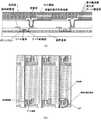
図2(a)〜(f)を参照して、本発明の第1の実施例に係る製造方法を工程順に説明する。第1の実施例は、例えば、第2の電極としてITO膜を形成する場合、まず、基盤10を用意し(図2(a))、当該基盤10を洗浄後、第1の電極12を形成する(図2(b))。次に、前記第1の電極12上に有機物材料膜14を通常の手法により形成する(図2(c))。図示された有機物材料膜14中には、発光層が含まれていることは言うまでも無い。 With reference to FIGS. 2A to 2F, the manufacturing method according to the first embodiment of the present invention will be described in the order of steps. In the first embodiment, for example, when forming an ITO film as the second electrode, first, the
次に、第2の電極を形成するが、本発明では、第2の電極の形成の際、先ず、図2(d)に示すように、InSnの金属合金材料等の非酸化金属材料をターゲット電極材料とするスパッタリング法で形成し、このInSnの金属合金材料膜18を1〜2nmの範囲の膜厚まで積層する。次に、図2(e)に示すように、プラズマ装置を用いた酸素ラジカルイオンを発生させたプラズマ条件下で酸化処理を行う。このとき、先に形成されたInSnの金属合金材料膜18は、活性な酸素ラジカルイオンによって酸化され、金属酸化膜材料(ここでは、ITO)膜18’に変換させる。このような方法で、第2の電極を形成すると、基材である有機物材料膜14の表面は金属酸化膜材料膜(酸化InSn膜)18’が酸化抑制のための保護膜になり、酸化ダメージやプラズマダメージを生じなくなる。 Next, the second electrode is formed. In the present invention, when forming the second electrode, first, as shown in FIG. 2D, a non-oxidized metal material such as an InSn metal alloy material is used as a target. The InSn metal
上記した工程は、真空を維持した雰囲気のもとで、あるいは、水分濃度を制御したN2ガス、またはドライエアーガスの雰囲気を維持した大気圧から100Torrまでの範囲の圧力のもとで、基盤を搬送し、連続して行なわれることが望ましい。 The above-mentioned process is performed under an atmosphere maintaining a vacuum, or under a pressure ranging from atmospheric pressure to 100 Torr maintaining an atmosphere of N2 gas or dry air gas with controlled moisture concentration. It is desirable to carry and carry out continuously.
最後に、第2の電極の導電率を向上させるために、InSnの金属合金材料膜などの非酸化金属材料膜をターゲット電極材料とするスパッタリング法で堆積速度を向上させたプロセス条件で形成し、このInSnの金属合金材料膜を100〜200nmの範囲の膜厚まで積層した後、金属酸化膜材料膜18’と同様に、当該金属酸化膜材料膜20に変換する。ここで、金属合金材料膜18’及び20としては、窒素を含んだ金属合金材料膜(窒化金属材料膜)を使うと、さらに酸化ダメージを低減できる。 Finally, in order to improve the conductivity of the second electrode, a non-oxidized metal material film such as a metal alloy material film of InSn is formed under a process condition with an improved deposition rate by sputtering using a target electrode material, After the InSn metal alloy material film is laminated to a thickness in the range of 100 to 200 nm, it is converted into the metal oxide
図3を参照して、本発明の第2の実施例に係る製造方法を工程順に説明する。この実施例は、例えば、第2の電極としてITO膜を形成する場合、まず、図3(a)に示すように、基盤10を用意し、この基盤10を洗浄後、第1の金属電極膜12を図3(b)に示すように形成する。次に、図3(c)に示すように、前記第1の金属電極膜12上に、発光層を含む有機物材料膜14を形成する。 With reference to FIG. 3, the manufacturing method according to the second embodiment of the present invention will be described in the order of steps. In this embodiment, for example, when forming an ITO film as the second electrode, first, as shown in FIG. 3A, a
更に、この実施例では、第2の電極を形成するために、図3(d)に示すように、先ず、InSnのような金属合金などの非酸化金属材料をターゲット電極材料とするスパッタリング法で形成し、このInSnの金属合金材料膜を1〜2nmの範囲の膜厚まで積層して、金属合金材料膜22を成膜する。 Furthermore, in this embodiment, in order to form the second electrode, as shown in FIG. 3D, first, a sputtering method using a non-oxide metal material such as a metal alloy such as InSn as a target electrode material is used. Then, this InSn metal alloy material film is laminated to a thickness in the range of 1 to 2 nm to form a metal
金属合金材料膜22上に、第1の実施例と同様に、InSnの金属合金材料膜18を成膜する。即ち、図示された金属合金材料膜は、非酸化金属材料をターゲット電極材料とするスパッタリング法で1〜2nmの膜厚まで積層される。続いて、当該金属合金材料膜18には、図3(e)に示すように、プラズマ装置を用いた酸素ラジカルイオンを発生させたプラズマ条件下で酸化処理が施される。この結果、先に形成されたInSnの金属合金材料膜は、活性な酸素ラジカルイオンによって酸化され、金属酸化膜材料(ここでは、ITO)膜18’に変換される。このように、プラズマ装置を用いた酸素ラジカルイオンを発生させたプラズマ条件下で酸化処理を行うと、先に形成されたInSnの金属合金材料膜18は、活性な酸素ラジカルイオンによって0.5〜1nmの範囲の膜厚まで酸化され、金属合金膜の表面層の一部を金属酸化膜材料(ITO)膜18’に変換される。 An InSn metal
更に、図3(f)に示すように、金属酸化膜材料膜18’上には、InSnの金属合金材料膜などの非酸化金属材料膜をターゲット電極材料とするスパッタリング法で堆積速度を向上させたプロセス条件で形成し、このInSnの金属合金膜材料を100〜200nmの範囲の膜厚まで積層した後、金属酸化膜材料膜18’と同様に、当該金属酸化膜材料膜20に変換する。ここで、金属合金材料膜18’及び20としては、窒素を含んだ単体金属または金属合金の材料膜(窒化金属材料膜)を使うと、さらに酸化ダメージを低減できる。 Further, as shown in FIG. 3 (f), the deposition rate is improved on the metal oxide film material film 18 'by sputtering using a non-oxide metal material film such as an InSn metal alloy material film as a target electrode material. After the InSn metal alloy film material is laminated to a thickness in the range of 100 to 200 nm, it is converted into the metal oxide
このような方法で、第2の電極を形成すると、基材である有機物材料の表面層は、界面層に残っている金属合金材料膜22が酸化抑制のための保護膜になり、酸化ダメージやプラズマダメージをさらに低減できる。 When the second electrode is formed by such a method, the surface layer of the organic material that is the base material becomes a protective film for suppressing the oxidation of the metal
図4を参照して、本発明の第3の実施例に係る製造方法を工程順に説明する。図4(a)、(b)、及び(c)に示すように、基盤10上に第1の金属電極膜12を成膜し、当該第1の金属電極膜12上に、有機物材料膜14を形成する点は前述した他の実施例と同様である。この実施例では、有機物材料膜14の保護膜として、図4(d)に示すように、非晶質の単元素金属材料膜24を有機物材料膜14上に形成している点で、他の実施例と相違している。この例では、In又はSn等を非酸化金属材料をターゲット材料とするスパッタリングが行なわれ、第1の単元素金属材料膜24が1nmの膜厚だけ成膜される。 With reference to FIG. 4, the manufacturing method according to the third embodiment of the present invention will be described in the order of steps. As shown in FIGS. 4A, 4B, and 4C, a first
次に、図4(e)に示すように、InまたはSnの第1の単元素金属材料膜24上に、InSnの第2の金属合金材料等の非酸化金属をターゲット電極材料とするスパッタリング法で形成し、このInSnの金属合金材料膜を1〜2nmの範囲の膜厚だけ積層して、金属合金材料膜18を形成する。次に、プラズマ装置を用いた酸素ラジカルイオンを発生させたプラズマ条件下で上層の第2の金属膜材料膜18のみを酸化処理して、図4(f)に示すように、第2の金属酸化物材料膜18’を形成する。このとき、図4(e)で形成されたInSnの第2金属合金材料膜18は、活性な酸素ラジカルイオンによって1〜2nmの範囲の膜厚だけ酸化され、第2の金属合金材料膜18のみが金属酸化膜材料(ITO)膜18’に変換される。このような方法で、第2の電極を形成すると、基材である有機物材料の表面は、界面層に保護膜として残っている単元素金属材料膜24により保護され、酸化ダメージやプラズマダメージを完全に抑制できる。 Next, as shown in FIG. 4E, a sputtering method using a non-oxidized metal such as a second metal alloy material of InSn on the first single element
最後に、第2の電極の導電率を向上させるために、InSnの金属合金材料膜などの非酸化金属材料膜をターゲット電極材料とするスパッタリング法で堆積速度を向上させたプロセス条件で形成し、このInSnの金属合金材料膜を100〜200nmの範囲の膜厚まで積層すると共に、当該金属合金材料膜を上記した酸化処理と同様に金属酸化物材料膜20にする。ここで、単元素金属膜材料、あるいは金属合金材料膜としては、窒素を含んだ金属合金材料膜を使うと、さらに酸化ダメージを低減できる。 Finally, in order to improve the conductivity of the second electrode, a non-oxidized metal material film such as a metal alloy material film of InSn is formed under a process condition with an improved deposition rate by sputtering using a target electrode material, The InSn metal alloy material film is laminated to a thickness in the range of 100 to 200 nm, and the metal alloy material film is made into the metal
図5を参照して、本発明の第4の実施例に係る製造方法を工程順に説明する。この実施例においても、第2の電極として、ITO膜を形成する場合を説明する。まず、基盤10(図5(a))を洗浄後、当該基盤10上に窒素を含む第1の金属電極膜12を第1の電極として成膜し(図5(b))、続いて、第1の電極上に有機物材料膜14を形成する。 With reference to FIG. 5, the manufacturing method which concerns on the 4th Example of this invention is demonstrated in order of a process. Also in this embodiment, the case where an ITO film is formed as the second electrode will be described. First, after cleaning the substrate 10 (FIG. 5A), a first
次に、有機物材料膜14上に第2の電極を形成するが、この実施例では、第2の電極の形成工程が他の実施例と異なっている。具体的に説明すると、先ず、InSnに窒素を含む第1の金属合金、あるいは窒素を含む金属などの非酸化金属材料をターゲット電極材料とするスパッタリング法で、InSnの合金または単体金属に窒素を含む非晶質の第1の窒化金属材料膜26が1nmの膜厚だけ成膜される(図5(d))。この場合、第1の窒化金属材料膜26は、上に述べたように単体金属たとえばInまたはSnと窒素を含む窒化金属材料膜であっても良い。 Next, a second electrode is formed on the
次に、図5(e)に示すように、窒化金属材料膜26上に、InSnと窒素を含む金属合金材料、あるいは、窒素を含む金属膜材料などの非酸化金属材料をターゲット電極材料とするスパッタリング法で、第2の窒化金属材料膜28が形成される。この場合、第2の窒化金属材料膜は1〜2nmの範囲の膜厚を有している。 Next, as shown in FIG. 5E, a non-oxide metal material such as a metal alloy material containing InSn and nitrogen or a metal film material containing nitrogen is used as a target electrode material on the metal
続いて、プラズマ装置を用いた酸素ラジカルイオンを発生させたプラズマ条件下で上層の第2の窒化金属材料膜28のみが酸化処理され、第2の窒化金属酸化物材料膜28’が形成される。このとき、第2の窒化金属材料膜28のみが活性な酸素ラジカルイオンによって1〜2nmの範囲の膜厚だけ酸化され、窒化金属酸化膜材料(ITO)膜28’に変換される。このような方法で、第2の電極を形成すると、基材である有機物材料の表面層は、界面層に一部分残っているInSn膜(第1の窒化金属材料膜26)が酸化抑制のための保護膜になり、酸化ダメージやプラズマダメージを完全に抑制できる。最後に、第2の電極の導電率を向上させるために、InSnと窒素を含む窒化金属合金材料などの非酸化金属材料をターゲット電極材料とするスパッタリング法で、堆積速度を向上させたプロセス条件で、窒化金属合金材料膜などの非酸化金属材料膜を100〜200nmの範囲の膜厚まで積層した後、前述と同様な酸化処理を行い、第2の窒化金属酸化物材料膜30を形成する。 Subsequently, only the upper second metal
なお、上記の実施例は全てトップエミッション型有機エレクトロルミネッセンス素子の製造方法に例をとり、かつその上部電極の形成に本発明を適用した場合について説明したが、下部電極の形成にも本発明を適用しても良い。また、図6(a)及び(b)、並びに、図8(a)及び(b)に断面図および平面図でそれぞれ示すボトムエミッション型有機エレクトロルミネッセンス素子の導電性透明電極(下部電極)の形成にも、さらにそれに加えて対向電極(上部電極)の形成にも本発明を適用できるし、図7(a)及び(b)、図8(a)及び(b)に一部断面図・平面図で示すようなアクティブマトリックス形のトップエミッション型およびボトムエミッション型有機エレクトロルミネッセンス素子の透明電極の形成、対向電極の形成にも本発明は適用できる。さらに、液晶表示装置の透明電極等の導電性酸化物電極または配線、半導体装置やその他あらゆる電子装置における導電性酸化物を含む電極または配線の形成に本発明は適用して効果がある。 In addition, although all the above embodiments have been described with respect to the method of manufacturing a top emission type organic electroluminescence element and the present invention is applied to the formation of the upper electrode, the present invention is also applied to the formation of the lower electrode. It may be applied. Also, the formation of the conductive transparent electrode (lower electrode) of the bottom emission type organic electroluminescence element shown in the sectional view and the plan view in FIGS. 6A and 6B and FIGS. 8A and 8B, respectively. Furthermore, in addition to this, the present invention can be applied to the formation of the counter electrode (upper electrode). FIGS. 7 (a) and 7 (b) and FIGS. 8 (a) and 8 (b) are partially sectional views and planes. The present invention can also be applied to the formation of transparent electrodes and counter electrodes of active matrix top emission type and bottom emission type organic electroluminescence elements as shown in the drawings. Furthermore, the present invention is effective when applied to the formation of conductive oxide electrodes or wirings such as transparent electrodes of liquid crystal display devices, and electrodes or wirings containing conductive oxides in semiconductor devices and all other electronic devices.
以上説明したように、本発明は有機エレクトロルミネッセンス素子、当該有機エレクトロルミネッセンス素子を含む表示装置、及び、表示装置を含む電子装置に適用できる。また、液晶表示装置の透明電極等の導電性酸化物電極または配線、半導体装置やその他あらゆる電子装置における導電性酸化物を含む電極または配線の形成にも本発明は適用できる。 As described above, the present invention can be applied to an organic electroluminescence element, a display device including the organic electroluminescence element, and an electronic device including the display device. The present invention can also be applied to the formation of conductive oxide electrodes or wirings such as transparent electrodes of liquid crystal display devices, and electrodes or wirings containing conductive oxides in semiconductor devices and all other electronic devices.
10 基盤
12 第1の金属電極膜
14 有機物材料膜
18 金属合金材料膜
18’ 金属酸化物材料膜
20 金属酸化物材料膜DESCRIPTION OF
Claims (48)
Translated fromJapaneseThe organic electroluminescent element manufactured by the manufacturing method as described in any one of Claims 1-16.
Priority Applications (2)
| Application Number | Priority Date | Filing Date | Title |
|---|---|---|---|
| JP2004089729AJP4817609B2 (en) | 2004-03-25 | 2004-03-25 | Method for manufacturing organic electroluminescence element and method for manufacturing display device |
| TW094131805ATW200714123A (en) | 2004-03-25 | 2005-09-15 | Method of producing an organic electroluminescence device |
Applications Claiming Priority (1)
| Application Number | Priority Date | Filing Date | Title |
|---|---|---|---|
| JP2004089729AJP4817609B2 (en) | 2004-03-25 | 2004-03-25 | Method for manufacturing organic electroluminescence element and method for manufacturing display device |
Publications (2)
| Publication Number | Publication Date |
|---|---|
| JP2005276689Atrue JP2005276689A (en) | 2005-10-06 |
| JP4817609B2 JP4817609B2 (en) | 2011-11-16 |
Family
ID=35176113
Family Applications (1)
| Application Number | Title | Priority Date | Filing Date |
|---|---|---|---|
| JP2004089729AExpired - Fee RelatedJP4817609B2 (en) | 2004-03-25 | 2004-03-25 | Method for manufacturing organic electroluminescence element and method for manufacturing display device |
Country Status (2)
| Country | Link |
|---|---|
| JP (1) | JP4817609B2 (en) |
| TW (1) | TW200714123A (en) |
Cited By (1)
| Publication number | Priority date | Publication date | Assignee | Title |
|---|---|---|---|---|
| JP2009295538A (en)* | 2008-06-09 | 2009-12-17 | Sony Corp | Manufacturing method for display unit, and display unit |
Citations (4)
| Publication number | Priority date | Publication date | Assignee | Title |
|---|---|---|---|---|
| JPS63266063A (en)* | 1987-04-23 | 1988-11-02 | Sharp Corp | ITO film creation method |
| JP2004031102A (en)* | 2002-06-25 | 2004-01-29 | Fuji Electric Holdings Co Ltd | Organic EL light emitting device and method of manufacturing the same |
| JP2004087369A (en)* | 2002-08-28 | 2004-03-18 | Nippon Sheet Glass Co Ltd | EL element sealing plate, method of manufacturing the same, and mother glass substrate for multi-cavity molding of the sealing plate |
| JP2004087321A (en)* | 2002-08-27 | 2004-03-18 | Konica Minolta Holdings Inc | Manufacturing method for organic electroluminescent element |
- 2004
- 2004-03-25JPJP2004089729Apatent/JP4817609B2/ennot_activeExpired - Fee Related
- 2005
- 2005-09-15TWTW094131805Apatent/TW200714123A/enunknown
Patent Citations (4)
| Publication number | Priority date | Publication date | Assignee | Title |
|---|---|---|---|---|
| JPS63266063A (en)* | 1987-04-23 | 1988-11-02 | Sharp Corp | ITO film creation method |
| JP2004031102A (en)* | 2002-06-25 | 2004-01-29 | Fuji Electric Holdings Co Ltd | Organic EL light emitting device and method of manufacturing the same |
| JP2004087321A (en)* | 2002-08-27 | 2004-03-18 | Konica Minolta Holdings Inc | Manufacturing method for organic electroluminescent element |
| JP2004087369A (en)* | 2002-08-28 | 2004-03-18 | Nippon Sheet Glass Co Ltd | EL element sealing plate, method of manufacturing the same, and mother glass substrate for multi-cavity molding of the sealing plate |
Cited By (3)
| Publication number | Priority date | Publication date | Assignee | Title |
|---|---|---|---|---|
| JP2009295538A (en)* | 2008-06-09 | 2009-12-17 | Sony Corp | Manufacturing method for display unit, and display unit |
| US7847477B2 (en) | 2008-06-09 | 2010-12-07 | Sony Corporation | Method of manufacturing display unit and display unit |
| TWI414203B (en)* | 2008-06-09 | 2013-11-01 | Sony Corp | A manufacturing method and a display device of a display device |
Also Published As
| Publication number | Publication date |
|---|---|
| JP4817609B2 (en) | 2011-11-16 |
| TW200714123A (en) | 2007-04-01 |
Similar Documents
| Publication | Publication Date | Title |
|---|---|---|
| US10522781B2 (en) | Electroluminescence device and display device | |
| US8927325B2 (en) | Method for producing an organic radiation-emitting component and organic radiation-emitting component | |
| KR100865445B1 (en) | Fabrication method for organic electronic device and organic electronic device fabricated by the same method | |
| KR20080010455A (en) | Manufacturing method of organic EL element, organic EL display apparatus, and organic EL element | |
| KR101010023B1 (en) | Manufacturing Method of Flexible Device Using Laser Beam | |
| KR100844788B1 (en) | Fabrication method for organic light emitting device and organic light emitting device fabricated by the same method | |
| US20070159071A1 (en) | Organic light emitting diode device | |
| KR20250090366A (en) | Opto-electronic device including an auxiliary electrode and a partition | |
| CN101405366B (en) | Fabrication method for organic light emitting device and organic light emitting device fabricated by the same method | |
| CN100420066C (en) | Organic electroluminescent element and display device comprising same | |
| US20050184650A1 (en) | [organic electro-luminescent device and fabricating method thereof] | |
| KR100784487B1 (en) | Electrode Formation Method of Organic Electroluminescent Device and Organic Electroluminescent Device Made Using the Same | |
| JP2011091093A (en) | Organic el element | |
| JP4817609B2 (en) | Method for manufacturing organic electroluminescence element and method for manufacturing display device | |
| JP2005032563A (en) | Film forming method, organic el element, and manufacturing method thereof | |
| US7628669B2 (en) | Organic light emitting devices with conductive layers having adjustable work function and fabrication methods thereof | |
| CN100426548C (en) | Organic Light Emitting Diode Structure | |
| TWI220852B (en) | An organic light emitting diode structure | |
| WO2007032062A1 (en) | Process for producing organic electroluminescence device | |
| KR100761112B1 (en) | Manufacturing method of electroluminescent device | |
| KR20100013522A (en) | Manufacturing method for organic light emitting display | |
| JP2004335206A (en) | Organic EL element and method of manufacturing the same | |
| KR100993145B1 (en) | Organic light emitting diode and method of manufacturing same | |
| WO2023159007A1 (en) | Amorphous metal based top emission organic light emitting diodes | |
| JP2009525579A (en) | Organic light emitting device manufacturing method and organic light emitting device manufactured thereby |
Legal Events
| Date | Code | Title | Description |
|---|---|---|---|
| A621 | Written request for application examination | Free format text:JAPANESE INTERMEDIATE CODE: A621 Effective date:20070305 | |
| A711 | Notification of change in applicant | Free format text:JAPANESE INTERMEDIATE CODE: A711 Effective date:20091207 | |
| A131 | Notification of reasons for refusal | Free format text:JAPANESE INTERMEDIATE CODE: A131 Effective date:20101005 | |
| A521 | Request for written amendment filed | Free format text:JAPANESE INTERMEDIATE CODE: A523 Effective date:20101206 | |
| TRDD | Decision of grant or rejection written | ||
| A01 | Written decision to grant a patent or to grant a registration (utility model) | Free format text:JAPANESE INTERMEDIATE CODE: A01 Effective date:20110823 | |
| A01 | Written decision to grant a patent or to grant a registration (utility model) | Free format text:JAPANESE INTERMEDIATE CODE: A01 | |
| A61 | First payment of annual fees (during grant procedure) | Free format text:JAPANESE INTERMEDIATE CODE: A61 Effective date:20110830 | |
| FPAY | Renewal fee payment (event date is renewal date of database) | Free format text:PAYMENT UNTIL: 20140909 Year of fee payment:3 | |
| FPAY | Renewal fee payment (event date is renewal date of database) | Free format text:PAYMENT UNTIL: 20140909 Year of fee payment:3 | |
| LAPS | Cancellation because of no payment of annual fees |