JP2005252293A - Semiconductor light emitting device - Google Patents
Semiconductor light emitting deviceDownload PDFInfo
- Publication number
- JP2005252293A JP2005252293AJP2005112809AJP2005112809AJP2005252293AJP 2005252293 AJP2005252293 AJP 2005252293AJP 2005112809 AJP2005112809 AJP 2005112809AJP 2005112809 AJP2005112809 AJP 2005112809AJP 2005252293 AJP2005252293 AJP 2005252293A
- Authority
- JP
- Japan
- Prior art keywords
- light emitting
- emitting device
- semiconductor light
- luminescence conversion
- semiconductor
- Prior art date
- Legal status (The legal status is an assumption and is not a legal conclusion. Google has not performed a legal analysis and makes no representation as to the accuracy of the status listed.)
- Granted
Links
Images


Classifications
- H—ELECTRICITY
- H10—SEMICONDUCTOR DEVICES; ELECTRIC SOLID-STATE DEVICES NOT OTHERWISE PROVIDED FOR
- H10H—INORGANIC LIGHT-EMITTING SEMICONDUCTOR DEVICES HAVING POTENTIAL BARRIERS
- H10H20/00—Individual inorganic light-emitting semiconductor devices having potential barriers, e.g. light-emitting diodes [LED]
- H10H20/80—Constructional details
- H10H20/85—Packages
- H10H20/851—Wavelength conversion means
- C—CHEMISTRY; METALLURGY
- C09—DYES; PAINTS; POLISHES; NATURAL RESINS; ADHESIVES; COMPOSITIONS NOT OTHERWISE PROVIDED FOR; APPLICATIONS OF MATERIALS NOT OTHERWISE PROVIDED FOR
- C09K—MATERIALS FOR MISCELLANEOUS APPLICATIONS, NOT PROVIDED FOR ELSEWHERE
- C09K11/00—Luminescent, e.g. electroluminescent, chemiluminescent materials
- C09K11/08—Luminescent, e.g. electroluminescent, chemiluminescent materials containing inorganic luminescent materials
- C09K11/77—Luminescent, e.g. electroluminescent, chemiluminescent materials containing inorganic luminescent materials containing rare earth metals
- C09K11/7715—Luminescent, e.g. electroluminescent, chemiluminescent materials containing inorganic luminescent materials containing rare earth metals containing cerium
- C09K11/7716—Chalcogenides
- C09K11/7718—Chalcogenides with alkaline earth metals
- C—CHEMISTRY; METALLURGY
- C09—DYES; PAINTS; POLISHES; NATURAL RESINS; ADHESIVES; COMPOSITIONS NOT OTHERWISE PROVIDED FOR; APPLICATIONS OF MATERIALS NOT OTHERWISE PROVIDED FOR
- C09K—MATERIALS FOR MISCELLANEOUS APPLICATIONS, NOT PROVIDED FOR ELSEWHERE
- C09K11/00—Luminescent, e.g. electroluminescent, chemiluminescent materials
- C09K11/08—Luminescent, e.g. electroluminescent, chemiluminescent materials containing inorganic luminescent materials
- C09K11/77—Luminescent, e.g. electroluminescent, chemiluminescent materials containing inorganic luminescent materials containing rare earth metals
- C09K11/7743—Luminescent, e.g. electroluminescent, chemiluminescent materials containing inorganic luminescent materials containing rare earth metals containing terbium
- C09K11/7744—Chalcogenides
- C09K11/7746—Chalcogenides with alkaline earth metals
- C—CHEMISTRY; METALLURGY
- C09—DYES; PAINTS; POLISHES; NATURAL RESINS; ADHESIVES; COMPOSITIONS NOT OTHERWISE PROVIDED FOR; APPLICATIONS OF MATERIALS NOT OTHERWISE PROVIDED FOR
- C09K—MATERIALS FOR MISCELLANEOUS APPLICATIONS, NOT PROVIDED FOR ELSEWHERE
- C09K11/00—Luminescent, e.g. electroluminescent, chemiluminescent materials
- C09K11/08—Luminescent, e.g. electroluminescent, chemiluminescent materials containing inorganic luminescent materials
- C09K11/77—Luminescent, e.g. electroluminescent, chemiluminescent materials containing inorganic luminescent materials containing rare earth metals
- C09K11/7766—Luminescent, e.g. electroluminescent, chemiluminescent materials containing inorganic luminescent materials containing rare earth metals containing two or more rare earth metals
- C09K11/7767—Chalcogenides
- C09K11/7769—Oxides
- C—CHEMISTRY; METALLURGY
- C09—DYES; PAINTS; POLISHES; NATURAL RESINS; ADHESIVES; COMPOSITIONS NOT OTHERWISE PROVIDED FOR; APPLICATIONS OF MATERIALS NOT OTHERWISE PROVIDED FOR
- C09K—MATERIALS FOR MISCELLANEOUS APPLICATIONS, NOT PROVIDED FOR ELSEWHERE
- C09K11/00—Luminescent, e.g. electroluminescent, chemiluminescent materials
- C09K11/08—Luminescent, e.g. electroluminescent, chemiluminescent materials containing inorganic luminescent materials
- C09K11/77—Luminescent, e.g. electroluminescent, chemiluminescent materials containing inorganic luminescent materials containing rare earth metals
- C09K11/7766—Luminescent, e.g. electroluminescent, chemiluminescent materials containing inorganic luminescent materials containing rare earth metals containing two or more rare earth metals
- C09K11/7774—Aluminates
- H—ELECTRICITY
- H10—SEMICONDUCTOR DEVICES; ELECTRIC SOLID-STATE DEVICES NOT OTHERWISE PROVIDED FOR
- H10H—INORGANIC LIGHT-EMITTING SEMICONDUCTOR DEVICES HAVING POTENTIAL BARRIERS
- H10H20/00—Individual inorganic light-emitting semiconductor devices having potential barriers, e.g. light-emitting diodes [LED]
- H10H20/80—Constructional details
- H10H20/85—Packages
- H10H20/8506—Containers
- H—ELECTRICITY
- H10—SEMICONDUCTOR DEVICES; ELECTRIC SOLID-STATE DEVICES NOT OTHERWISE PROVIDED FOR
- H10H—INORGANIC LIGHT-EMITTING SEMICONDUCTOR DEVICES HAVING POTENTIAL BARRIERS
- H10H20/00—Individual inorganic light-emitting semiconductor devices having potential barriers, e.g. light-emitting diodes [LED]
- H10H20/80—Constructional details
- H10H20/85—Packages
- H10H20/851—Wavelength conversion means
- H10H20/8511—Wavelength conversion means characterised by their material, e.g. binder
- H10H20/8512—Wavelength conversion materials
- H—ELECTRICITY
- H01—ELECTRIC ELEMENTS
- H01L—SEMICONDUCTOR DEVICES NOT COVERED BY CLASS H10
- H01L2224/00—Indexing scheme for arrangements for connecting or disconnecting semiconductor or solid-state bodies and methods related thereto as covered by H01L24/00
- H01L2224/01—Means for bonding being attached to, or being formed on, the surface to be connected, e.g. chip-to-package, die-attach, "first-level" interconnects; Manufacturing methods related thereto
- H01L2224/26—Layer connectors, e.g. plate connectors, solder or adhesive layers; Manufacturing methods related thereto
- H01L2224/31—Structure, shape, material or disposition of the layer connectors after the connecting process
- H01L2224/32—Structure, shape, material or disposition of the layer connectors after the connecting process of an individual layer connector
- H01L2224/321—Disposition
- H01L2224/32151—Disposition the layer connector connecting between a semiconductor or solid-state body and an item not being a semiconductor or solid-state body, e.g. chip-to-substrate, chip-to-passive
- H01L2224/32221—Disposition the layer connector connecting between a semiconductor or solid-state body and an item not being a semiconductor or solid-state body, e.g. chip-to-substrate, chip-to-passive the body and the item being stacked
- H01L2224/32245—Disposition the layer connector connecting between a semiconductor or solid-state body and an item not being a semiconductor or solid-state body, e.g. chip-to-substrate, chip-to-passive the body and the item being stacked the item being metallic
- H01L2224/32257—Disposition the layer connector connecting between a semiconductor or solid-state body and an item not being a semiconductor or solid-state body, e.g. chip-to-substrate, chip-to-passive the body and the item being stacked the item being metallic the layer connector connecting to a bonding area disposed in a recess of the surface of the item
- H—ELECTRICITY
- H01—ELECTRIC ELEMENTS
- H01L—SEMICONDUCTOR DEVICES NOT COVERED BY CLASS H10
- H01L2224/00—Indexing scheme for arrangements for connecting or disconnecting semiconductor or solid-state bodies and methods related thereto as covered by H01L24/00
- H01L2224/01—Means for bonding being attached to, or being formed on, the surface to be connected, e.g. chip-to-package, die-attach, "first-level" interconnects; Manufacturing methods related thereto
- H01L2224/42—Wire connectors; Manufacturing methods related thereto
- H01L2224/47—Structure, shape, material or disposition of the wire connectors after the connecting process
- H01L2224/48—Structure, shape, material or disposition of the wire connectors after the connecting process of an individual wire connector
- H01L2224/4805—Shape
- H01L2224/4809—Loop shape
- H01L2224/48091—Arched
- H—ELECTRICITY
- H01—ELECTRIC ELEMENTS
- H01L—SEMICONDUCTOR DEVICES NOT COVERED BY CLASS H10
- H01L2224/00—Indexing scheme for arrangements for connecting or disconnecting semiconductor or solid-state bodies and methods related thereto as covered by H01L24/00
- H01L2224/01—Means for bonding being attached to, or being formed on, the surface to be connected, e.g. chip-to-package, die-attach, "first-level" interconnects; Manufacturing methods related thereto
- H01L2224/42—Wire connectors; Manufacturing methods related thereto
- H01L2224/47—Structure, shape, material or disposition of the wire connectors after the connecting process
- H01L2224/48—Structure, shape, material or disposition of the wire connectors after the connecting process of an individual wire connector
- H01L2224/481—Disposition
- H01L2224/48151—Connecting between a semiconductor or solid-state body and an item not being a semiconductor or solid-state body, e.g. chip-to-substrate, chip-to-passive
- H01L2224/48221—Connecting between a semiconductor or solid-state body and an item not being a semiconductor or solid-state body, e.g. chip-to-substrate, chip-to-passive the body and the item being stacked
- H01L2224/48245—Connecting between a semiconductor or solid-state body and an item not being a semiconductor or solid-state body, e.g. chip-to-substrate, chip-to-passive the body and the item being stacked the item being metallic
- H01L2224/48247—Connecting between a semiconductor or solid-state body and an item not being a semiconductor or solid-state body, e.g. chip-to-substrate, chip-to-passive the body and the item being stacked the item being metallic connecting the wire to a bond pad of the item
- H—ELECTRICITY
- H01—ELECTRIC ELEMENTS
- H01L—SEMICONDUCTOR DEVICES NOT COVERED BY CLASS H10
- H01L2224/00—Indexing scheme for arrangements for connecting or disconnecting semiconductor or solid-state bodies and methods related thereto as covered by H01L24/00
- H01L2224/01—Means for bonding being attached to, or being formed on, the surface to be connected, e.g. chip-to-package, die-attach, "first-level" interconnects; Manufacturing methods related thereto
- H01L2224/42—Wire connectors; Manufacturing methods related thereto
- H01L2224/47—Structure, shape, material or disposition of the wire connectors after the connecting process
- H01L2224/48—Structure, shape, material or disposition of the wire connectors after the connecting process of an individual wire connector
- H01L2224/481—Disposition
- H01L2224/48151—Connecting between a semiconductor or solid-state body and an item not being a semiconductor or solid-state body, e.g. chip-to-substrate, chip-to-passive
- H01L2224/48221—Connecting between a semiconductor or solid-state body and an item not being a semiconductor or solid-state body, e.g. chip-to-substrate, chip-to-passive the body and the item being stacked
- H01L2224/48245—Connecting between a semiconductor or solid-state body and an item not being a semiconductor or solid-state body, e.g. chip-to-substrate, chip-to-passive the body and the item being stacked the item being metallic
- H01L2224/48257—Connecting between a semiconductor or solid-state body and an item not being a semiconductor or solid-state body, e.g. chip-to-substrate, chip-to-passive the body and the item being stacked the item being metallic connecting the wire to a die pad of the item
- H—ELECTRICITY
- H01—ELECTRIC ELEMENTS
- H01L—SEMICONDUCTOR DEVICES NOT COVERED BY CLASS H10
- H01L2224/00—Indexing scheme for arrangements for connecting or disconnecting semiconductor or solid-state bodies and methods related thereto as covered by H01L24/00
- H01L2224/01—Means for bonding being attached to, or being formed on, the surface to be connected, e.g. chip-to-package, die-attach, "first-level" interconnects; Manufacturing methods related thereto
- H01L2224/42—Wire connectors; Manufacturing methods related thereto
- H01L2224/47—Structure, shape, material or disposition of the wire connectors after the connecting process
- H01L2224/48—Structure, shape, material or disposition of the wire connectors after the connecting process of an individual wire connector
- H01L2224/484—Connecting portions
- H01L2224/48463—Connecting portions the connecting portion on the bonding area of the semiconductor or solid-state body being a ball bond
- H01L2224/48465—Connecting portions the connecting portion on the bonding area of the semiconductor or solid-state body being a ball bond the other connecting portion not on the bonding area being a wedge bond, i.e. ball-to-wedge, regular stitch
- H—ELECTRICITY
- H01—ELECTRIC ELEMENTS
- H01L—SEMICONDUCTOR DEVICES NOT COVERED BY CLASS H10
- H01L2224/00—Indexing scheme for arrangements for connecting or disconnecting semiconductor or solid-state bodies and methods related thereto as covered by H01L24/00
- H01L2224/01—Means for bonding being attached to, or being formed on, the surface to be connected, e.g. chip-to-package, die-attach, "first-level" interconnects; Manufacturing methods related thereto
- H01L2224/42—Wire connectors; Manufacturing methods related thereto
- H01L2224/47—Structure, shape, material or disposition of the wire connectors after the connecting process
- H01L2224/48—Structure, shape, material or disposition of the wire connectors after the connecting process of an individual wire connector
- H01L2224/484—Connecting portions
- H01L2224/4847—Connecting portions the connecting portion on the bonding area of the semiconductor or solid-state body being a wedge bond
- H01L2224/48472—Connecting portions the connecting portion on the bonding area of the semiconductor or solid-state body being a wedge bond the other connecting portion not on the bonding area also being a wedge bond, i.e. wedge-to-wedge
- H—ELECTRICITY
- H01—ELECTRIC ELEMENTS
- H01L—SEMICONDUCTOR DEVICES NOT COVERED BY CLASS H10
- H01L2224/00—Indexing scheme for arrangements for connecting or disconnecting semiconductor or solid-state bodies and methods related thereto as covered by H01L24/00
- H01L2224/01—Means for bonding being attached to, or being formed on, the surface to be connected, e.g. chip-to-package, die-attach, "first-level" interconnects; Manufacturing methods related thereto
- H01L2224/42—Wire connectors; Manufacturing methods related thereto
- H01L2224/47—Structure, shape, material or disposition of the wire connectors after the connecting process
- H01L2224/49—Structure, shape, material or disposition of the wire connectors after the connecting process of a plurality of wire connectors
- H01L2224/491—Disposition
- H01L2224/49105—Connecting at different heights
- H01L2224/49107—Connecting at different heights on the semiconductor or solid-state body
- H—ELECTRICITY
- H01—ELECTRIC ELEMENTS
- H01L—SEMICONDUCTOR DEVICES NOT COVERED BY CLASS H10
- H01L2224/00—Indexing scheme for arrangements for connecting or disconnecting semiconductor or solid-state bodies and methods related thereto as covered by H01L24/00
- H01L2224/73—Means for bonding being of different types provided for in two or more of groups H01L2224/10, H01L2224/18, H01L2224/26, H01L2224/34, H01L2224/42, H01L2224/50, H01L2224/63, H01L2224/71
- H01L2224/732—Location after the connecting process
- H01L2224/73251—Location after the connecting process on different surfaces
- H01L2224/73265—Layer and wire connectors
- H—ELECTRICITY
- H01—ELECTRIC ELEMENTS
- H01L—SEMICONDUCTOR DEVICES NOT COVERED BY CLASS H10
- H01L2224/00—Indexing scheme for arrangements for connecting or disconnecting semiconductor or solid-state bodies and methods related thereto as covered by H01L24/00
- H01L2224/80—Methods for connecting semiconductor or other solid state bodies using means for bonding being attached to, or being formed on, the surface to be connected
- H01L2224/85—Methods for connecting semiconductor or other solid state bodies using means for bonding being attached to, or being formed on, the surface to be connected using a wire connector
- H01L2224/85909—Post-treatment of the connector or wire bonding area
- H01L2224/8592—Applying permanent coating, e.g. protective coating
- H—ELECTRICITY
- H01—ELECTRIC ELEMENTS
- H01L—SEMICONDUCTOR DEVICES NOT COVERED BY CLASS H10
- H01L2924/00—Indexing scheme for arrangements or methods for connecting or disconnecting semiconductor or solid-state bodies as covered by H01L24/00
- H01L2924/01—Chemical elements
- H01L2924/01021—Scandium [Sc]
- H—ELECTRICITY
- H01—ELECTRIC ELEMENTS
- H01L—SEMICONDUCTOR DEVICES NOT COVERED BY CLASS H10
- H01L2924/00—Indexing scheme for arrangements or methods for connecting or disconnecting semiconductor or solid-state bodies as covered by H01L24/00
- H01L2924/01—Chemical elements
- H01L2924/01079—Gold [Au]
- H—ELECTRICITY
- H01—ELECTRIC ELEMENTS
- H01L—SEMICONDUCTOR DEVICES NOT COVERED BY CLASS H10
- H01L2924/00—Indexing scheme for arrangements or methods for connecting or disconnecting semiconductor or solid-state bodies as covered by H01L24/00
- H01L2924/10—Details of semiconductor or other solid state devices to be connected
- H01L2924/11—Device type
- H01L2924/12—Passive devices, e.g. 2 terminal devices
- H01L2924/1204—Optical Diode
- H01L2924/12041—LED
- H—ELECTRICITY
- H01—ELECTRIC ELEMENTS
- H01L—SEMICONDUCTOR DEVICES NOT COVERED BY CLASS H10
- H01L2924/00—Indexing scheme for arrangements or methods for connecting or disconnecting semiconductor or solid-state bodies as covered by H01L24/00
- H01L2924/10—Details of semiconductor or other solid state devices to be connected
- H01L2924/11—Device type
- H01L2924/12—Passive devices, e.g. 2 terminal devices
- H01L2924/1204—Optical Diode
- H01L2924/12044—OLED
- H—ELECTRICITY
- H01—ELECTRIC ELEMENTS
- H01L—SEMICONDUCTOR DEVICES NOT COVERED BY CLASS H10
- H01L2924/00—Indexing scheme for arrangements or methods for connecting or disconnecting semiconductor or solid-state bodies as covered by H01L24/00
- H01L2924/15—Details of package parts other than the semiconductor or other solid state devices to be connected
- H01L2924/181—Encapsulation
- H—ELECTRICITY
- H10—SEMICONDUCTOR DEVICES; ELECTRIC SOLID-STATE DEVICES NOT OTHERWISE PROVIDED FOR
- H10H—INORGANIC LIGHT-EMITTING SEMICONDUCTOR DEVICES HAVING POTENTIAL BARRIERS
- H10H20/00—Individual inorganic light-emitting semiconductor devices having potential barriers, e.g. light-emitting diodes [LED]
- H10H20/80—Constructional details
- H10H20/85—Packages
- H10H20/851—Wavelength conversion means
- H10H20/8511—Wavelength conversion means characterised by their material, e.g. binder
- H—ELECTRICITY
- H10—SEMICONDUCTOR DEVICES; ELECTRIC SOLID-STATE DEVICES NOT OTHERWISE PROVIDED FOR
- H10H—INORGANIC LIGHT-EMITTING SEMICONDUCTOR DEVICES HAVING POTENTIAL BARRIERS
- H10H20/00—Individual inorganic light-emitting semiconductor devices having potential barriers, e.g. light-emitting diodes [LED]
- H10H20/80—Constructional details
- H10H20/85—Packages
- H10H20/852—Encapsulations
- H10H20/854—Encapsulations characterised by their material, e.g. epoxy or silicone resins
- H—ELECTRICITY
- H10—SEMICONDUCTOR DEVICES; ELECTRIC SOLID-STATE DEVICES NOT OTHERWISE PROVIDED FOR
- H10H—INORGANIC LIGHT-EMITTING SEMICONDUCTOR DEVICES HAVING POTENTIAL BARRIERS
- H10H20/00—Individual inorganic light-emitting semiconductor devices having potential barriers, e.g. light-emitting diodes [LED]
- H10H20/80—Constructional details
- H10H20/882—Scattering means
- Y—GENERAL TAGGING OF NEW TECHNOLOGICAL DEVELOPMENTS; GENERAL TAGGING OF CROSS-SECTIONAL TECHNOLOGIES SPANNING OVER SEVERAL SECTIONS OF THE IPC; TECHNICAL SUBJECTS COVERED BY FORMER USPC CROSS-REFERENCE ART COLLECTIONS [XRACs] AND DIGESTS
- Y02—TECHNOLOGIES OR APPLICATIONS FOR MITIGATION OR ADAPTATION AGAINST CLIMATE CHANGE
- Y02B—CLIMATE CHANGE MITIGATION TECHNOLOGIES RELATED TO BUILDINGS, e.g. HOUSING, HOUSE APPLIANCES OR RELATED END-USER APPLICATIONS
- Y02B20/00—Energy efficient lighting technologies, e.g. halogen lamps or gas discharge lamps
Landscapes
- Chemical & Material Sciences (AREA)
- Inorganic Chemistry (AREA)
- Engineering & Computer Science (AREA)
- Materials Engineering (AREA)
- Organic Chemistry (AREA)
- Led Device Packages (AREA)
- Led Devices (AREA)
- Luminescent Compositions (AREA)
- Liquid Crystal (AREA)
Abstract
Translated fromJapaneseDescription
Translated fromJapanese本発明は、半導体発光素子の作動中に電磁ビームを放射する半導体基体と、この半導体基体と導電的に接続されている少なくとも1つの第1の電気接続端子及び少なくとも1つの第2の電気接続端子と、少なくとも1つの蛍光物質を有するルミネセンス変換エレメントとを備えた半導体発光素子に関する。 The present invention includes a semiconductor substrate that emits an electromagnetic beam during operation of a semiconductor light emitting device, at least one first electrical connection terminal and at least one second electrical connection terminal that are conductively connected to the semiconductor substrate. And a luminescence conversion element having at least one fluorescent material.
このような半導体素子は、例えば、DE3804293から公知である。ここには、エレクトロルミネセンスダイオード又はレーザダイオードが記載されており、レーザダイオードでは、ダイオードから放射された放射スペクトル全体が光変換作用をする発光有機色素の混じったプラスチックから成るエレメントを用いて、比較的大きな波長の方へシフトされる。それにより、装置機構から放射された光は、発光ダイオードから放射された光とは別の色を有する。プラスチックに添加された色素の種類に依存して、同一の発光ダイオードタイプにより、種々の色で発光する発光ダイオードを作製できる。 Such a semiconductor element is known, for example, from DE 3804293. Here, an electroluminescent diode or laser diode is described, in which the entire emission spectrum emitted from the diode is compared using an element made of a plastic mixed with a luminescent organic dye that acts as a light converter. Shifted toward larger wavelengths. Thereby, the light emitted from the device mechanism has a different color from the light emitted from the light emitting diode. Depending on the type of dye added to the plastic, light-emitting diodes that emit light in various colors can be produced with the same light-emitting diode type.
DE−OS2347289から公知の赤外線(IR)固体ランプでは、IRダイオードの縁にて、蛍光物質が取り付けられており、この蛍光物質は、そこから放射されたIRビームを可視光に変換する。この手段の目標は、コントロール目的のため、IRビームのできるだけ僅かな部分を、放射されたIRビームの強度の低減をできるだけ僅かにして、可視光に変換することである。 In the infrared (IR) solid-state lamp known from DE-OS 2347289, a fluorescent material is attached at the edge of the IR diode, which converts the IR beam emitted from it into visible light. The goal of this measure is to convert as little part of the IR beam to visible light as possible for control purposes, with as little reduction in the intensity of the emitted IR beam as possible.
更にEP486052から公知の発光ダイオードではサブストレートとアクティブなエレクトロルミネセンス層との間に少なくとも1つの半導体フォトルミネセンス層が設けられており、このフォトルミネセンス層はアクティブ層からサブストレートの方へ放射された第1の波長領域の光を第2の波長領域の光へ変換し、その結果発光ダイオードは全体として相異なる波長領域の光を放射する。 Furthermore, in the light-emitting diodes known from EP 486052, at least one semiconductor photoluminescent layer is provided between the substrate and the active electroluminescent layer, which photoluminescent layer emits from the active layer towards the substrate. The light in the first wavelength region is converted into light in the second wavelength region, and as a result, the light emitting diode emits light in different wavelength regions as a whole.
発光ダイオードの数多の潜在的に可能の適用分野、例えば車両計器盤における指示素子、航空機及び自動車における照明並びに、フルカラーに適したLEDディスプレイの場合にて、混合光、殊に白色光を発することができる発光ダイオードに対する要求が強く現れている。 Emitting mixed light, especially white light, in the case of a large number of light-emitting diodes, for example in the case of indicator elements in vehicle instrument panels, lighting in aircraft and automobiles, and LED displays suitable for full color There is a strong demand for light emitting diodes that can be used.
JP−07176794−Aでは、白色光を放射する平面形光源が記載されており、この平面形光源では、透明板の1つの端面にて青色光を発する2つのダイオードが設けられており、この2つのダイオードは光を透明板内に放射する。透明板は相対向する2つの主面の上に蛍光作用をする物質で被覆されており、この蛍光物質はダイオードの青色光で励起されると光を発する。蛍光物質から発せられた光は、ダイオードから発せられた青色光とは別の波長を有する。上記の公知の半導体発光素子では、光源が均質な白色光を放射するように発光物質を被着することは特に困難である。更に、量産上の再現可能性も大きな問題となる。それというのは、例えば透明板の表面の非平坦性に基づく発光層の僅かな厚層の変動だけでもう、放射された光の白色相の変化が惹起されるからである。
本発明の課題は、均質な混合光を放射し、極めて十分に再現可能な素子特性を以て技術的に簡単な量産を保証するように、冒頭で述べたような半導体発光素子を発展させることである。 The object of the present invention is to develop a semiconductor light-emitting device as described at the outset so as to emit a homogeneously mixed light and guarantee a technically simple mass production with extremely well-reproducible device characteristics. .
この課題は、半導体基体が半導体多層構造を有し、半導体多層構造は半導体発光素子の作動中に、少なくとも青色スペクトル領域又は緑色スペクトル領域から成るビームを包含する第1の波長領域の電磁ビームを放射し、ルミネセンス変換エレメントは、第1の波長領域に由来するビームを第1の波長領域とは異なる第2の波長領域に変換し、半導体発光素子は第1の波長領域のビーム及び第2の波長領域のビームから成る混合ビームを放射し、ルミネセンス変換エレメントは、蛍光材料を包含するシリコン材料から製造されている、ルミネセンス変換層および/またはルミネセンス変換エンベロープを有することにより解決される。 The problem is that the semiconductor substrate has a semiconductor multilayer structure, and the semiconductor multilayer structure emits an electromagnetic beam in a first wavelength region including a beam composed of at least a blue spectral region or a green spectral region during operation of the semiconductor light emitting device. The luminescence conversion element converts the beam derived from the first wavelength region into a second wavelength region different from the first wavelength region, and the semiconductor light emitting element includes the first wavelength region beam and the second wavelength region. A mixed beam consisting of a beam in the wavelength region is emitted and the luminescence conversion element is solved by having a luminescence conversion layer and / or a luminescence conversion envelope made of a silicon material including a fluorescent material.
本発明の有利な発展形態が請求項2から19に記載されている。 Advantageous developments of the invention are described in
本発明によれば、発光半導体基体は多層構造、例え、GaxIn1−xN又はGaxAl1−xNから成る活性半導体層を有する多層構造を有し、この多層構造は半導体素子の作動中に紫外線スペクトル領域、青色スペクトル領域及び/又は緑色スペクトル領域から成る第1の波長領域の電磁ビームを放射するものである。ルミネセンス変換エレメントは、第1の波長領域に由来するビームを、第1の波長領域1とは異なる第2の波長領域のビームに変換し、ここで、半導体発光素子は第1の波長領域のビーム及び第2の波長領域のビームから成る混合ビームを放射する。換言すれば、例えばルミネセンス変換エレメントは、半導体発光素子から放射されるビームを有利には、第1の波長領域のスペクトル部分領域に亘ってスペクトル的に選択的に吸収し、比較的長い波長の領域(第2の波長領域)において放射する。有利には、半導体発光素子から放射されるビームはλ≦520nmのもとで相対的な強度最大値を有し、ルミネセンス変換エレメントによりスペクトル的に選択的に吸収された波長領域はこの強度最大値から外れたところに位置する。According to the invention, the light-emitting semiconductor substrate has a multilayer structure, for example a multilayer structure having an active semiconductor layer made of Gax In1-x N or Gax Al1-x N, which multilayer structure is During operation, it emits an electromagnetic beam of a first wavelength region consisting of an ultraviolet spectral region, a blue spectral region and / or a green spectral region. The luminescence conversion element converts a beam derived from the first wavelength region into a beam of a second wavelength region different from the
同様に有利には、本発明によれば第1の波長領域に由来する複数の(1つ又は1つより多くの)第1のスペクトル部分領域を複数の第2の波長領域に変換することができる。それにより、多様の色混合及び色温度を生じさせることが可能である。 Equally advantageously, according to the invention, a plurality (one or more) of the first spectral sub-regions originating from the first wavelength region can be converted into a plurality of second wavelength regions. it can. Thereby, various color mixing and color temperatures can be generated.
本発明の半導体発光素子は、ルミネセンス変換を介して生じた波長スペクトル、ひいては放射された光の色が半導体発光素子を通る動作電流強度の高さに依存しないという特別な利点を有する。このことは半導体発光素子の周囲温度、従って動作電流強度も著しく変動する場合特に大きな重要性を有する。GaNをベースとする半導体発光素子を有する特別な発光ダイオードは、これに関して著しく敏感である。 The semiconductor light emitting device of the present invention has the particular advantage that the wavelength spectrum generated through luminescence conversion and thus the color of the emitted light does not depend on the high operating current intensity through the semiconductor light emitting device. This is particularly important when the ambient temperature of the semiconductor light emitting device, and thus the operating current intensity, varies significantly. Special light-emitting diodes with semiconductor light-emitting elements based on GaN are very sensitive in this regard.
更に本発明の半導体発光素子は単一の制御電圧しか必要とせず、したがってまた単一の制御回路装置しか必要とせず、それによって半導体発光素子の制御回路に対する構成部品コストを著しく僅かに抑えることができる。 Furthermore, the semiconductor light emitting device of the present invention requires only a single control voltage, and therefore only a single control circuit device, thereby significantly reducing the component cost for the control circuit of the semiconductor light emitting device. it can.
本発明の特に有利な実施形態によれば、ルミネセンス変換エレメントとして、半導体基体上に、又はその上方に、部分的に透明なルミネセンス変換層、即ち、発光半導体基体から放射されるビームに対して部分的に透過性であるルミネセンス変換層が設けられている。放射された光の統一的な色を確保するため、ルミネセンス変換層は全く一定の厚さを有するように構成されている。このことにより得られる特別な利点は、ルミネセンス変換層を通って半導体基体から放射される光の光路長が、全てのビーム方向に対してほぼ一定であることである。これによって半導体発光素子が全ての方向で同一色の光を放射することが達成される。この本発明の発展形態による半導体発光素子のさらなる特別な利点は、簡単な手法で高い再現性を達成できることであり、このことは、効率的な量産にとって極めて重要な意義がある。ルミネセンス変換層として、例えば蛍光物質の添加されたラッカ層又は樹脂層を設けるとよい。 According to a particularly advantageous embodiment of the invention, as a luminescence conversion element, on or above a semiconductor substrate, a partially transparent luminescence conversion layer, i.e. for a beam emitted from a light-emitting semiconductor substrate. A luminescence conversion layer is provided which is partially transparent. In order to ensure a uniform color of the emitted light, the luminescence conversion layer is configured to have a completely constant thickness. A special advantage obtained by this is that the optical path length of the light emitted from the semiconductor substrate through the luminescence conversion layer is substantially constant for all beam directions. This achieves that the semiconductor light emitting device emits light of the same color in all directions. A further special advantage of the semiconductor light emitting device according to the development of the present invention is that high reproducibility can be achieved by a simple method, which is extremely important for efficient mass production. As the luminescence conversion layer, for example, a lacquer layer or a resin layer to which a fluorescent substance is added may be provided.
本発明の半導体発光素子の他の有利な実施形態によれば、ルミネセンス変換エレメントとして部分的に透明なルミネセンス変換エンベロープが設けられており、このルミネセンス変換エンベロープは、半導体基体の少なくとも1部(及び電気接続端子の部分領域)を包囲するように構成されており、同時に構成部品カバー(ケーシング)として利用することができる。この実施形態による半導体発光素子の利点は、実質的に、従来の発光ダイオード(例えば、ラジアル発光ダイオード(Radial-Leuchtdiode))の作製のため使用される生産ラインをこの半導体発光素子の作製に利用できることである。構成部品エンベロープのため、従来の発光ダイオードにおいてそのために使用される透明なプラスチックの代わりに、ルミネセンス変換エンベロープの材料が使用される。 According to another advantageous embodiment of the semiconductor light-emitting device according to the invention, a partially transparent luminescence conversion envelope is provided as the luminescence conversion element, which luminescence conversion envelope is at least part of the semiconductor substrate. (And a partial region of the electrical connection terminal) is surrounded, and can be used as a component cover (casing) at the same time. The advantage of the semiconductor light emitting device according to this embodiment is that a production line used for manufacturing a conventional light emitting diode (for example, a radial light emitting diode (Radial-Leuchtdiode)) can be used for manufacturing the semiconductor light emitting device. It is. Because of the component envelope, the material of the luminescence conversion envelope is used instead of the transparent plastic used for it in conventional light emitting diodes.
本発明の半導体発光素子の更なる有利な実施形態及び上記の2つの有利な実施形態ではルミネセンス変換層ないしルミネセンス変換エンベロープは、透明な材料、例えばプラスチック、有利にはエポキシ樹脂(有利なプラスチック及び蛍光物質の事例が、更に以下示されている)から成る。そのようにして、ルミネセンス変換エレメントを特に有利なコストで作製できる。即ち、そのために必要な方法ステップは、大きなコストを掛けずに発光ダイオードのための従来の生産ラインに統合化可能である。 In a further advantageous embodiment of the semiconductor light-emitting device according to the invention and in the two advantageous embodiments described above, the luminescence conversion layer or the luminescence conversion envelope is made of a transparent material, for example a plastic, preferably an epoxy resin (advantageous plastic). And examples of fluorescent materials are further shown below). In that way, a luminescence conversion element can be produced at a particularly advantageous cost. That is, the method steps required for this can be integrated into a conventional production line for light-emitting diodes without significant costs.
本発明の有利な発展形態によれば、1つ又は複数の第2の波長領域は、実質的に、第1の波長領域より大きな波長λを有しているのである。 According to an advantageous development of the invention, the one or more second wavelength regions have a wavelength λ which is substantially larger than the first wavelength region.
殊に、本発明の更なる実施形態によれば、第1の波長領域の第2の部分スペクトル領域及び第2の波長領域は相互に相補的である。そのようにして単一のカラーの光源、殊に青色光を放射する単一の半導体基体を有する発光ダイオードから混色の光、殊に白色光を発生させることができる。例えば青色光を放射する半導体基体により白色光を発生させるために、半導体基体から放射されるビームの部分が、青色のスペクトル領域から青色に対して補色の黄色のスペクトル領域に変換される。白色光の色温度又は色個所は、ルミネセンス変換エレメントの適当な選定により、殊に、蛍光物質ないしそれの粒子の大きさ及びそれの濃度の適当な選定により可変できる。更に、前記配置構成は、有利には蛍光物質の混合体を使用できるようにするものであり、これによって有利に所望の色相を著しく精確に調節できる。同様にルミネセンス変換エレメントを、例えば不均質な蛍光物質分布により、不均質に構成することもできる。これにより有利にはルミネセンス変換エレメントを通る光の種々の光路長を補償できる。 In particular, according to a further embodiment of the invention, the second partial spectral region and the second wavelength region of the first wavelength region are complementary to each other. In this way it is possible to generate mixed color light, in particular white light, from a single color light source, in particular a light emitting diode with a single semiconductor substrate emitting blue light. For example, in order to generate white light by a semiconductor substrate that emits blue light, a portion of the beam emitted from the semiconductor substrate is converted from a blue spectral region to a yellow spectral region complementary to blue. The color temperature or color location of white light can be varied by appropriate selection of the luminescence conversion element, in particular by appropriate selection of the size of the phosphor or its particles and their concentration. Furthermore, the arrangement advantageously makes it possible to use a mixture of phosphors, which advantageously allows the desired hue to be adjusted very precisely. Similarly, the luminescence conversion element can also be configured inhomogeneously, for example by a heterogeneous phosphor distribution. This advantageously compensates for the various optical path lengths of the light passing through the luminescence conversion element.
本発明の有利な実施形態では、ルミネセンス変換エレメント又は構成部品エンベロープの他の構成部分が色整合のため1つ又は複数の色素を有し、この色素は波長変換を行わせないものである。このために、従来の発光ダイオードの作製に使用された色素、例えばアゾ系色素、アントラキノン系色素又はペリノン系色素を使用できる。 In an advantageous embodiment of the invention, the other components of the luminescence conversion element or component envelope have one or more dyes for color matching, which dyes do not perform wavelength conversion. For this purpose, it is possible to use dyes used in the production of conventional light emitting diodes, such as azo dyes, anthraquinone dyes or perinone dyes.
過度に高いビーム負荷からルミネセンス変換エレメントを保護するために、本発明の有利な実施形態ないし前記半導体発光素子の有利な実施形態によれば、半導体基体の表面の少なくとも一部が第1のエンベロープ、例えばプラスチックから成る第1の透明なエンベロープにより被覆され、このエンベロープ上にルミネセンス変換層が被着されるのである。それにより、ルミネセンス変換エレメントにおけるビーム密度、従って、それのビーム負荷が低減され、このことは使用される材料に応じて、ルミネセンス変換エレメントの耐用寿命に好ましい影響を及ぼす。 In order to protect the luminescence conversion element from excessively high beam loads, according to an advantageous embodiment of the invention or an advantageous embodiment of the semiconductor light emitting device, at least a part of the surface of the semiconductor substrate is a first envelope. It is covered by a first transparent envelope made of plastic, for example, and a luminescence conversion layer is deposited on this envelope. Thereby, the beam density in the luminescence conversion element and thus its beam load is reduced, which has a positive effect on the useful life of the luminescence conversion element, depending on the material used.
本発明の特に有利な構成及び前述の実施形態では発光半導体基体が使用され、この発光半導体基体では、半導体基体から放射されたビームスペクトルが波長420nmと460nmとの間、殊に430nm(例えばGaxAl1−xNをベースとした半導体基体)又は450nm(例えばGaxIn1−xNをベースとした半導体基体)での波長のもとでルミネセンス強度最大値を有する。そのような本発明の半導体発光素子により、有利にはC.I.Eカラーチャートのほぼ全ての色及び混色を生じさせることができる。ここで、発光半導体基体は上述のように、実質的に、エレクトロルミネセンス半導体材料から成っていてよいが、他の半導体材料から成っていてもよく、例えば他のエレクトロルミネセンス半導体材料、例えばポリマ材料から成っていてもよい。In a particularly advantageous configuration of the invention and in the above-mentioned embodiments, a light-emitting semiconductor substrate is used, in which the beam spectrum emitted from the semiconductor substrate has a wavelength between 420 nm and 460 nm, in particular 430 nm (for example Gax It has a maximum luminescence intensity at a wavelength at 450 nm (eg a semiconductor substrate based on Gax In1-x N) or a semiconductor substrate based on Al1-x N. With such a semiconductor light emitting device of the present invention, C.I. I. Almost all colors and mixed colors of the E color chart can be generated. Here, as described above, the light emitting semiconductor substrate may be substantially made of an electroluminescent semiconductor material, but may be made of another semiconductor material, for example, another electroluminescent semiconductor material such as a polymer. It may consist of materials.
本発明の更なる特に有利な発展形態では、ルミネセンス変換エンベロープないしルミネセンス変換層は、ラッカ又はプラスチック、例えばオプトエレクトロニック構成素子のエンベロープに使用されるシリコン材料、熱可塑性材料又は熱硬化性材料(エポキシ樹脂及びアクリル樹脂)から作製される。更に、例えば熱可塑性材料から製造された被覆体をルミネセンス変換エンベロープとして使用できる。上述の全ての材料に簡単に1つ又は複数の蛍光物質を添加することができる。 In a further particularly advantageous development of the invention, the luminescence conversion envelope or the luminescence conversion layer is a lacquer or plastic, for example a silicon material, a thermoplastic material or a thermosetting material (used for the envelope of an optoelectronic component). Made of epoxy resin and acrylic resin). Furthermore, for example, coatings made from thermoplastic materials can be used as the luminescence conversion envelope. One or more phosphors can simply be added to all the materials mentioned above.
本発明の半導体発光素子は次のようにすれば特に簡単に実現できる。即ち、半導体基体は、場合により事前に製造されたケーシングの切欠部内に配置されており、この切欠部にはルミネセンス変換層を有する被覆体が設けられている。その種の半導体発光素子を従来の生産ラインで量産的に作製できる。このために、ケーシング中への半導体基体の組付後、被覆部材、例えばラッカ層又は射出成形樹脂層、又は熱可塑性材料から成る事前に製造されている被覆板をケーシング上に被着しさえすればよい。オプショナル的にケーシングの切欠部を、透明な材料例えば透明なプラスチックで充填でき、この透明なプラスチックは、殊に半導体基体から放射される光の波長を変化させず、又は必要な場合には既にルミネセンス変換作用をするように構成することができる。 The semiconductor light emitting device of the present invention can be realized particularly easily as follows. That is, the semiconductor substrate is disposed in a cutout portion of a casing manufactured in advance according to circumstances, and a covering body having a luminescence conversion layer is provided in the cutout portion. Such a type of semiconductor light emitting device can be mass-produced on a conventional production line. For this purpose, after assembly of the semiconductor substrate in the casing, a covering member, for example a lacquer layer or an injection-molded resin layer, or even a pre-manufactured covering plate made of a thermoplastic material, can even be deposited on the casing. That's fine. Optionally, the cutout in the casing can be filled with a transparent material, for example a transparent plastic, which does not change the wavelength of the light emitted from the semiconductor substrate, or is already luminescent if necessary. It can be configured to have a sense conversion action.
特に簡単な実現可能性に基づき特に有利な本発明の半導体発光素子の発展形態では、半導体基体は、場合により事前に製造された、また必要に応じて既にリードフレームを備えたケーシング内に設けられ、切欠部は少なくとも部分的に透明な射出成形樹脂で充填され、この樹脂には蛍光物質が切欠部の注入前に既に添加されている。従ってここでは、ルミネセンス変換エレメントは、蛍光物質を備えた半導体基体の射出成形体を有する。 In a particularly advantageous development of the semiconductor light-emitting device according to the invention, which is particularly advantageous on the basis of a simple feasibility, the semiconductor substrate is optionally provided in a pre-manufactured casing and, if necessary, already provided with a lead frame. The notch is at least partially filled with a transparent injection molding resin, and a fluorescent material is already added to the resin before the notch is injected. Therefore, here, the luminescence conversion element has an injection molded body of a semiconductor substrate provided with a fluorescent material.
ルミネセンス変換エレメントの作製のための特に有利な材料は、1つ又は複数の蛍光物質の添加されているエポキシ樹脂である。但しエポキシ樹脂の代わりに、ポリメタクリル酸メチル(PMMA)を使用することもできる。 A particularly advantageous material for the production of the luminescence conversion element is an epoxy resin to which one or more phosphors are added. However, polymethyl methacrylate (PMMA) can be used instead of the epoxy resin.
PMMAには、簡単に有機の色素粒子を混入することができる。緑色、黄色、赤色で発光する本発明の半導体発光素子の作製のため、例えばペリレンをベースとした色素分子を使用できる。紫外線、可視又は赤外線領域で発光する半導体発光素子を4f有機金属化合物の混入によって作製することもできる。殊に赤色に発光する本発明の半導体発光素子を、例えば、Eu3+に基づく金属有機性キレート(λ≒620nm)の混合により実現できる。赤外線ビームを放射する半導体発光素子、殊に、赤色を放射する半導体基体を、4fキレート又はTi3+ドーピングされたサファイヤの混入により作製できる。PMMA can be easily mixed with organic pigment particles. For production of the semiconductor light emitting device of the present invention that emits green, yellow and red light, for example, dye molecules based on perylene can be used. A semiconductor light-emitting element that emits light in the ultraviolet, visible, or infrared region can also be fabricated by mixing a 4f organometallic compound. In particular, the semiconductor light emitting device of the present invention that emits red light can be realized, for example, by mixing a metal organic chelate (λ≈620 nm) based on Eu3+ . A semiconductor light emitting device that emits an infrared beam, in particular, a semiconductor substrate that emits red light, can be produced by mixing 4f chelate or Ti3+ doped sapphire.
白色光を放射する本発明の半導体発光素子は、有利に次のようにして作製できる。即ち、半導体基体から放射された青色ビームが補色の波長領域、殊に青と黄、又は加法的色トリオ、例えば青、緑、赤に変換されるように蛍光物質を選定するのである。ここで、黄色光ないし緑色光及び赤色光は蛍光物質を介して生ぜしめられる。これによって生じた白色の色相(CIEカラーチャートにおける色個所)を、混合及び濃度に関し1つ又は複数の色素の適当な選定により変化させることができる。 The semiconductor light emitting device of the present invention that emits white light can be advantageously manufactured as follows. That is, the fluorescent material is selected so that the blue beam emitted from the semiconductor substrate is converted into a complementary wavelength region, in particular blue and yellow, or an additive color trio, such as blue, green, red. Here, yellow light, green light, and red light are generated through the fluorescent material. The resulting white hue (color location in the CIE color chart) can be changed by appropriate selection of one or more dyes for mixing and density.
白色光を放射する本発明の半導体発光素子の適当な有機の蛍光物質は、例えば、緑のルミネセンスに対してはBASF Lumogen F 083、黄のルミネセンスに対してはBASF Lumogen F240、赤のルミネセンスに対してはBASF Lumogen F300のようなペリレン蛍光物質である。これらの色素を簡単に、例えば透明なエポキシ樹脂に添加することができる。 Suitable organic phosphors of the semiconductor light emitting device of the present invention that emit white light are, for example, BASF Lumogen F 083 for green luminescence, BASF Lumogen F240 for yellow luminescence, red luminescence. For the sense, it is a perylene fluorescent material such as BASF Lumogen F300. These dyes can be easily added to, for example, a transparent epoxy resin.
青色を放射する半導体基体により緑色を放射する半導体基体を作製する有利な方法によればルミネセンス変換エレメントに対して、UO2++置換されたホウケイ酸ガラス(Borsilikat)を使用する。According to an advantageous method for producing a green-emitting semiconductor substrate by means of a blue-emitting semiconductor substrate, UO2+ + substituted borosilicate glass (Borsilikat) is used for the luminescence conversion element.
本発明の半導体発光素子ないし上述の有利な実施形態の更なる有利な発展形態によれば、ルミネセンス変換エレメント又は構成部品エンベロープの他のビーム透過性のコンポーネントに、付加的に光分散する粒子、いわゆるディフューザ、拡散体が添加される。これによって有利には半導体発光素子の色印象及び放射特性を最適化できる。 According to a further advantageous development of the semiconductor light-emitting device of the invention or of the above-mentioned advantageous embodiments, particles that additionally disperse light into the luminescence conversion element or other beam-transmissive components of the component envelope, A so-called diffuser or diffuser is added. This advantageously optimizes the color impression and radiation characteristics of the semiconductor light emitting device.
本発明の半導体発光素子の特に有利な実施形態では、ルミネセンス変換エレメントは、少なくとも部分的に無機の蛍光物質を有する透明なエポキシ樹脂から成る。即ち、有利には、無機の蛍光物質を簡単にエポキシ樹脂内でバインディングできるからである。白色で発光する本発明の半導体発光素子の作製のための特に有利な無機の蛍光物質はYAG:Ce(Y3Al5O12:Ce3+)である。この蛍光物質を、殊に簡単に従来のLED技術にて使用された透明なエポキシ樹脂内に混入できる。更に、蛍光物質として可能なものは、稀土類でドーピングされたガーネット例えばY3Ga5O12:Ce3+及びY(Al,Ga)5O12:Ce3+及びY(Al,Ga)5O12:Tb3+並びに稀土類でドーピングされたアルカリ土類硫化物、例えばSrS:Ce3+、Na、SrS:Ce3+、Cl、SrS:CeCl3、CaS:Ce3+及びSrSe:Ce3+である。In a particularly advantageous embodiment of the semiconductor light-emitting device according to the invention, the luminescence conversion element consists of a transparent epoxy resin having at least partly an inorganic fluorescent material. That is, advantageously, the inorganic fluorescent material can be easily bound in the epoxy resin. A particularly advantageous inorganic fluorescent material for the production of the semiconductor light emitting device of the present invention that emits white light is YAG: Ce (Y3 Al5 O12 : Ce3+ ). This phosphor can be mixed in the transparent epoxy resin used in the conventional LED technology in a particularly simple manner. Further possible phosphors are rare earth doped garnets such as Y3 Ga5 O12 : Ce3+ and Y (Al, Ga)5 O12 : Ce3+ and Y (Al, Ga)5 O12. : Tb3+ and rare earth doped alkaline earth sulfides such as SrS: Ce3+ , Na, SrS: Ce3+ , Cl, SrS: CeCl3 , CaS: Ce3+ and SrSe: Ce3+ .
種々の混色の光の生成に適するのは、特に稀土類でドーピングされたチオガレート(Thiogallate)、例えば、CaGa2S4:Ce3+及びSrGa2S4:Ce3+である。同様に稀土類でドーピングされたアルミン酸塩、例えばYAlO3:Ce3+、YGaO3:Ce3+、Y(Al,Ga)O3:Ce3+及び稀土類でドーピングされたオルト珪酸塩M2SiO5:Ce3+(M:Sc,Y,Sc)例えばY2SiO5:Ce3+も使用可能である。全てのイットリウム化合物において基本的にイットリウムを、スカンジウム又はランタンで置換できる。Suitable for the generation of light of various colors is particularly rare earth doped thiogallate, such as CaGa2 S4 : Ce3+ and SrGa2 S4 : Ce3+ . Similarly rare earth doped aluminates such as YAlO3 : Ce3+ , YGaO3 : Ce3+ , Y (Al, Ga) O3 : Ce3+ and rare earth doped orthosilicate M2 SiO5 : Ce3+ (M: Sc, Y, Sc) For example, Y2 SiO5 : Ce3+ can also be used. In all yttrium compounds, essentially yttrium can be replaced by scandium or lanthanum.
本発明の半導体発光素子の更なる可能な実施形態において、エンベロープの光を透過させる少なくとも全てのコンポーネント、即ち、ルミネセンス変換エンベロープないし変換層も無機の材料だけから成る。従って、ルミネセンス変換エレメントは、無機の蛍光物質から成り、この無機の蛍光物質は温度安定性の透明又は部分的に透明の無機の材料内に埋込まれている。殊に、ルミネセンス変換エレメントは無機の蛍光物質から成り、この無機の蛍光物質は有利には低融点の無機ガラス(例えば珪酸塩ガラス)内に埋込まれている。このようなルミネセンス変換層の有利な作製法はゾル・ゲル技術であり、このゾル・ゲル技術によりルミネセンス変換層全体、即ち無機の蛍光物質のみならず、埋込材料をも1つの作業工程にて作製できる。 In a further possible embodiment of the semiconductor light emitting device according to the invention, at least all components that transmit the light of the envelope, i.e. the luminescence conversion envelope or conversion layer, also consist solely of inorganic materials. Thus, the luminescence conversion element consists of an inorganic phosphor, which is embedded in a temperature-stable transparent or partially transparent inorganic material. In particular, the luminescence conversion element consists of an inorganic phosphor, which is preferably embedded in a low-melting inorganic glass (for example silicate glass). An advantageous method for producing such a luminescence conversion layer is the sol-gel technique, which allows not only the entire luminescence conversion layer, that is, the inorganic fluorescent material but also the embedded material to be processed in one working step. Can be produced.
半導体基体から放射された第1の波長領域のビームを、ルミネセンス変換された第2の波長領域のビームと混合すること、ひいては放射された光の色均質性を改善するため、本発明によるルミネセンスエンベローブないしルミネセンス変換層及び/又はルミネセンス変換エンベローブの他のコンポーネントの半導体発光素子の有利な実施形態では、青色で発光する色素が添加され、この青色で発光する色素は半導体基体から放射されたビームのいわゆる指向特性を減衰する。指向特性とは、半導体基体から放射されたビームが特定の放射方向を有することを意味する。 In order to mix the first wavelength region beam emitted from the semiconductor substrate with the luminescence converted second wavelength region beam and thus to improve the color homogeneity of the emitted light, the luminescence according to the invention is used. In an advantageous embodiment of the semiconductor light-emitting device of the sense envelope or the luminescence conversion layer and / or the other components of the luminescence conversion envelope, a blue-emitting dye is added, which emits from the semiconductor substrate. Attenuates the so-called directivity of the beam. The directivity characteristic means that the beam emitted from the semiconductor substrate has a specific radiation direction.
本発明の半導体発光素子の有利な実施形態では、放射されたビームの混合の上記目的のため粉末の形態の無機の蛍光物質が使用され、ここで、蛍光物質の粒子はこれを包む材料(マトリクス)内では溶けない。更に、無機の蛍光物質及びこれを包む材料は相互に異なる屈折率を有する。それにより蛍光物質の粒度に依存して、蛍光物質により吸収されなかった光の成分が分散される。それにより、半導体基体から放射されたビームの指向特性が効率的に減衰され、その結果吸収されなかったビーム及びルミネセンス変換されたビームが均質に混合され、このことは空間的に均質の色印象を生じさせる。 In an advantageous embodiment of the semiconductor light-emitting device according to the invention, an inorganic phosphor in the form of a powder is used for the purpose of mixing the emitted beams, where the phosphor particles are the material (matrix) enclosing it. It does not melt in). Furthermore, the inorganic fluorescent material and the material enclosing it have different refractive indexes. Thereby, depending on the particle size of the fluorescent material, the components of the light not absorbed by the fluorescent material are dispersed. This effectively attenuates the directivity of the beam emitted from the semiconductor substrate, resulting in a homogeneous mixing of the unabsorbed beam and the luminescence converted beam, which is a spatially homogeneous color impression. Give rise to
白色光を放射する本発明の半導体発光素子は、特に有利には、ルミネセンス変換エンベローブ又は変換層の作製に使用されるエポキシ樹脂に無機の蛍光物質YAG:Ce(Y3Al5O12:Ce3+)が混合されていることによって実現できる。半導体基体から放射される青色ビームの一部が無機の蛍光物質Y3Al5O12:Ce3+により黄色スペクトル領域に、従って、青色に対して補色の波長領域にシフトされる。白色光の色相(CIEカラーチャートにおける色個所)を色素混合及び色素濃度により変化させることができる。The semiconductor light-emitting device of the present invention that emits white light is particularly preferably used as an inorganic fluorescent substance YAG: Ce (Y3 Al5 O12 : Ce) in an epoxy resin used for producing a luminescence conversion envelope or conversion layer.3+ ) is mixed. A part of the blue beam emitted from the semiconductor substrate is shifted to the yellow spectral region by the inorganic phosphor Y3 Al5 O12 : Ce3+ and thus to the wavelength region complementary to blue. The hue of white light (color location in the CIE color chart) can be changed by the dye mixture and the dye concentration.
更に無機の蛍光物質YAG:Ceは特に、ほぼ1.84の屈折率を有する非溶性色素(10μmの領域の粒度)であるという特別な利点を有する。これによって波長変換のほかに分散効果も生じ、この分散効果により青色のダイオードビーム及び黄色の変換ビームの混合が生じる。 Furthermore, the inorganic fluorescent substance YAG: Ce has the particular advantage of being an insoluble dye (particle size in the region of 10 μm) having a refractive index of approximately 1.84. This causes a dispersion effect in addition to the wavelength conversion, and this dispersion effect causes mixing of the blue diode beam and the yellow conversion beam.
本発明の半導体発光素子の更なる有利な発展形態では、ルミネセンス変換エレメント又は構成部品エンベローブの他のビーム透過性のコンポーネントに、付加的に光分散性の粒子、いわゆるディフューザ、拡散体が添加される。これによって、有利に半導体発光素子の色印象及び放射特性を更に一層最適化できる。 In a further advantageous development of the semiconductor light-emitting device according to the invention, light-dispersing particles, so-called diffusers, diffusers are additionally added to the luminescence conversion element or other beam-transmissive components of the component envelope. The This can advantageously further optimize the color impression and radiation characteristics of the semiconductor light emitting device.
特別な利点とするところは、白色発光する本発明の半導体発光素子ないしそれの上記の実施形態の発光効率が実質的にGaNをベースとして作製された青色発光する半導体基体について白熱灯の発光効率と同等であることである。その理由は、一方ではその種の半導体基体の外部量子収率が数%であり、他方では有機の色素分子の発光効率がしばしば90%以上のところに定在的に位置していることにある。更に本発明の半導体発光素子は、白熱灯に比して極めて長い耐用寿命、一層より大きい頑丈性及び一層より小さい動作電圧という優れた特長を有する。 The special advantage is that the semiconductor light-emitting device of the present invention that emits white light or the light-emitting efficiency of the above-described embodiment is substantially the same as the luminous efficiency of an incandescent lamp with respect to a semiconductor substrate that emits blue light based on GaN. It is equivalent. The reason is that, on the one hand, the external quantum yield of such a semiconductor substrate is a few percent, and on the other hand, the luminous efficiency of organic dye molecules is often located more than 90%. . Furthermore, the semiconductor light emitting device of the present invention has excellent features such as extremely long service life, greater robustness and lower operating voltage than incandescent lamps.
本発明の半導体発光素子の肉眼にとって知覚可能な明るさを、ルミネセンス変換エレメントの設けられていないが他の点では同一である半導体発光素子に比して著しく高めることができる。何故ならば視感特性は波長が高くなるほうに向かって増大するからである。 The brightness perceivable by the naked eye of the semiconductor light emitting device of the present invention can be significantly increased as compared with a semiconductor light emitting device which is not provided with a luminescence conversion element but is otherwise the same. This is because the visual characteristics increase toward higher wavelengths.
さらに本発明の基本的手法により有利には、可視光ビームのほかに半導体基体から放射される紫外線ビームを可視光に変換できる。これによって、半導体基体から放射される光の明るさが著しく高められる。 In addition to the visible light beam, the basic technique of the present invention advantageously converts an ultraviolet beam emitted from the semiconductor substrate into visible light. Thereby, the brightness of the light emitted from the semiconductor substrate is remarkably increased.
半導体基体の青色光を以てのルミネセンス変換のここで論じられるコンセプトを有利に下記のシェーマに従って、多段のルミネセンス変換エレメントに拡大し得る。即ち、紫外線→青色→緑色→黄色→赤色というシェーマに従って拡大し得る。ここでスペクトル的に選択的に放射する複数のルミネセンス変換エレメントが半導体基体に対して相対的に相前後して配置される。 The concept discussed here of luminescence conversion with blue light of a semiconductor substrate can be advantageously extended to a multi-stage luminescence conversion element according to the following schema. That is, it can be enlarged according to a schema of ultraviolet rays → blue → green → yellow → red. Here, a plurality of luminescence conversion elements that radiate spectrally selectively are arranged one after the other relative to the semiconductor substrate.
同様に有利に複数の種々の選択的に放射をする色素分子を共に、ルミネセンス変換エレメントの透明なプラスチック内に埋込むことができる。これにより著しく広幅の色スペクトルを生成できる。 Likewise, a plurality of different selectively emitting dye molecules can advantageously be embedded together in the transparent plastic of the luminescence conversion element. Thereby, a remarkably wide color spectrum can be generated.
ルミネセンス変換材料として、殊にYAG:Ceが使用されるようにした本発明の白色光を放射する半導体発光素子の特別な利点は、この蛍光物質が青色光で励起の際、吸収と放射との間でほぼ100nmのスペクトルシフトを生じさせることにある。それにより、蛍光物質から放射された光の再吸収の著しい低減、ひいては一層高い発光効率が得られる。更に、YAG:Ceは、有利に高い熱的及び光化学的(例えばUV−)安定性(これは有機の蛍光物質より遥かに高い)を有し、その結果、外部での使用及び/又は高温領域向けの白色光で発光するダイオードも作製可能である。 The special advantage of the semiconductor light emitting device emitting white light according to the present invention, in particular YAG: Ce used as the luminescence conversion material, is that when the phosphor is excited with blue light, it absorbs and emits light. A spectral shift of approximately 100 nm between the two. As a result, a significant reduction in reabsorption of light emitted from the fluorescent material, and thus a higher luminous efficiency can be obtained. Furthermore, YAG: Ce has advantageously high thermal and photochemical (eg UV-) stability (which is much higher than organic phosphors), so that it can be used externally and / or in the high temperature range. It is also possible to produce a diode that emits light with white light.
YAG:Ceはこれまで、再吸収、発光効率、熱的及び光化学的安定及び処理性に関して最も適している蛍光物質であることが判明している。但し、他のCeドーピングされた蛍光物質、殊にCeドーピングされたガーネットも可能である。 YAG: Ce has so far been found to be the most suitable fluorescent material with respect to reabsorption, luminous efficiency, thermal and photochemical stability and processability. However, other Ce-doped phosphors, in particular Ce-doped garnets, are also possible.
特に有利には、本発明の半導体発光素子をそれのわずかな低い消費電力に基づき、フルカラーに適したLEDディスプレイにて、車両内部空間又は航空機キャビンを照明するため、並びに車両計器盤又は液晶指示部のような指示装置を照明するために使用できる。 Particularly advantageously, the semiconductor light-emitting device according to the invention is based on its slightly low power consumption, with a LED display suitable for full color, for illuminating the vehicle interior space or aircraft cabin, as well as the vehicle instrument panel or liquid crystal indicator. Can be used to illuminate pointing devices such as
本発明の更なる特徴点、利点及び有用性は、図1〜14に関連した9つの実施例に対する以降の説明から明らかとなる。 Further features, advantages and utilities of the present invention will become apparent from the following description of the nine embodiments associated with FIGS.
図1に示す半導体発光素子は、半導体基体1と、背面コンタクト11と、前面コンタクト12と、複数の様々の層から成る多層構造7とを有し、この多層構造7は、半導体素子の作動中、1つのビーム(例えば、紫外線、青色又は緑色)を放射する少なくとも1つのアクティブなゾーンを有する。 The semiconductor light emitting device shown in FIG. 1 has a
この実施例及び以下述べる全ての実施例に対する適当な多層構造7を図9に示す。ここで、例えばSiCから成るサブストレート18上に、AlN層又はGaN層19、n導電形GaN層20、n導電形GaxAl1−xN層又はGaxIn1−xN層21、更なるn導電形GaN層又はGaxIn1−xN層22、p導電形GaxAl1−xN層又はGaxIn1−xN層23及びp導電形GaN層24から成る多層構造7が被着されている。p導電形GaN層24主面25上及びサブストレート18の主面26上に、それぞれ、コンタクト金属化部27、28が被着されている。このコンタクト金属化部27、28は、従来、電気的コンタクトのためのオプトエレクトロニクス半導体技術にて使用された材料から成る。A suitable multilayer structure 7 for this embodiment and all the embodiments described below is shown in FIG. Here, on a
しかしながら、本発明の半導体素子に対して当業者に適当と思われる何れの任意の他の半導体素子をも使用することができる。このことは、以下述べる全ての実施例に対しても成り立つ。 However, any other semiconductor element deemed appropriate to those skilled in the art for the semiconductor element of the present invention can be used. This is also true for all embodiments described below.
図1の実施例では、半導体基体1は導電性結合手段、例えば、金属性ろう又は接着剤を用いて、第1の電気接続端子2上の背面電極コンタクト11に取り付けられている。前面電極コンタクト12は、ボンディング線ワイヤ14を用いて第2の電気接続端子3に接続されている。 In the embodiment of FIG. 1, the
半導体基体1の自由な表面及び電気接続端子2及び3は、直接的にルミネセンス変換エンベローブ5により包囲されている。このルミネセンス変換エンベローブ5は、有利には、透明な発光ダイオードエンベローブに使用可能な透明なプラスチック(有利にはエポキシ樹脂又はポリメタクリル酸メチル)から成り、これには、白色光で発光する構成素子用の蛍光物質6、有利には無機の蛍光物質、有利にはY3Al5O12:Ce3+(YAG:Ce)が添加されている。The free surface of the
図2に示す本発明の半導体発光素子の実施例が図1に示す本発明の半導体発光素子の実施例と相異する点は、半導体基体1及び電気接続端子2及び3の部分領域がルミネセンス変換エンベローブにより包囲されているのではなく、透明なエンベロープ15により包囲されていることである。この透明なエンベロープ15は、半導体基体1により放射されたビームの波長変化を生じさせないものであり、例えば、発光ダイオード技術で従来使用されているエポキシ樹脂、シリコン樹脂又はアクリル樹脂又は他の適当なビーム透過性の材料、例えば、無機ガラスから成る。 The embodiment of the semiconductor light emitting device of the present invention shown in FIG. 2 is different from the embodiment of the semiconductor light emitting device of the present invention shown in FIG. 1 in that the
このエンベローブ15上にルミネセンス変換層4が被着されており、このルミネセンス変換層4は、図2に示すようにエンベローブ15の表面全体を被う。同様に、ルミネセンス変換層4がこの表面の単に一部のみを被うことも可能である。ルミネセンス変換層4は、例えば同じく透明なプラスチック(例えば、エポキシ樹脂、ラッカ、又は、ポリメタクリル酸メチル)から成り、これには蛍光物質6が添加されている。この場合も、白色発光する半導体発光素子に対する蛍光物質としては有利にはYAG:Ceが好適である。 The
前記の実施例の有する特別な利点とするところは、半導体基体から放射されるビーム全体に対して、ルミネセンス変換エレメントを通る光路長が等しくなることである。このことは殊に、しばしば起こるように、半導体発光素子から放射される光の精確な色相がこの光路長に依存する場合には特別な重要性を有する。 A special advantage of the above embodiment is that the optical path length through the luminescence conversion element is equal for the entire beam emitted from the semiconductor substrate. This is of particular importance when the exact hue of light emitted from the semiconductor light emitting device depends on this path length, as often happens.
図2のルミネセンス変換層4からの光の一層良好な出力結合のため、構成素子の一方の側面にレンズ状の被覆体29(破線で示す)を設けることができ、このレンズ状の被覆体29は、ルミネセンス変換層4内でのビームの全反射を低減するものである。上記のレンズ状の被覆体29は透明なプラスチック又はガラスから成ってよく、ルミネセンス変換層4上に、例えば接着されたり、又は直接ルミネセンス変換層4の構成部分として構成されてもよい。 For better output coupling of light from the
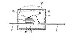
図3に示す実施例では第1及び第2電気接続端子2、3は不透過性の、場合によっては事前に製造された基底ケーシング8内に埋込まれている。事前に製造されたとは、半導体基体が電気接続端子2に取付られる前に基底ケーシング8が、既に電気接続端子2、3にて例えば射出成形により仕上がり完了しているということである。基底ケーシング8は、例えば不透過性のプラスチックから成り、切欠部9はそれの形状に関して作動中半導体基体から放射されたビーム(場合により内壁の適当なコーティングにより、)に対する反射器17として構成されている。そのようなケーシング8は、殊にプリント配線上に表面実装可能な発光ダイオードの場合使用される。上記ケーシングは半導体基体の取付前に、電気接続端子2、3を有する導体バンド(リードフレーム)上に、例えば射出成形により被着される。 In the embodiment shown in FIG. 3, the first and second
切欠部は9はルミネセンス変換層4により被われており、このルミネセンス変換層4としては、例えば、別個に作成されていて、ケーシング上に取り付けられたプラスチックから成る被覆板17により被われている。ルミネセンス変換層4に対する適当な材料としては同様に明細書冒頭説明部分において説明したプラスチック又は無機ガラスがそこに掲げられた蛍光物質と関連づけて対象と成る。切欠部9は透明なプラスチック、無機ガラス又はガスで充填されても良く、また真空状態にされてもよい。 The
図2の実施例におけるように、ここでもルミネセンス変換層4からの光の一層良好な出力結合のため、このルミネセンス変換層4上にレンズ状の被覆体29(破線で示す)を設けることもでき、この被覆体29はルミネセンス変換層4内でのビームの全反射を低減するものである。この被覆体は透明なプラスチックから成ってよく、ルミネセンス変換層4上に例えば接着したり、又はルミネセンス変換層4と共に一体的に形成されてもよい。 As in the embodiment of FIG. 2, a lens-shaped covering 29 (shown by a broken line) is provided on the
特に有利な実施形態では切欠部9は、図10に示すように、蛍光物質を有するエポキシ樹脂、即ちルミネセンスエンベローブ5で充填されており、このルミネセンスエンベローブ5はルミネセンス変換エレメントを形成する。被覆体17及び/又はレンズ状の被覆体29は省いてもよい。更に、オプショナルであるのは、図13に示すように第1の電気接続端子2が、例えばスタンピングにより半導体基体1の領域に反射器ウエル34として構成され、この反射器ウエル34はルミネセンス変換エンベローブで充填されている。 In a particularly advantageous embodiment, the
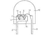
図4には、更なる実施例としてラジアルダイオードが示されている。ここで、半導体基体1は、第1の電気接続端子2の、反射器として構成された部分16内に例えばろう付け又は接着により取り付けられている。その種のケーシング構成形態は、発光ダイオード技術では公知であり、従って、説明を要しない。 FIG. 4 shows a radial diode as a further embodiment. Here, the
図4の実施例では半導体基体1は、透明なエンベローブ15により包囲されており、この透明なエンベロープ15は2番目に挙げた実施例(図2)におけるように、半導体基体1から放射されるビームの波長変化を生じさせず、従来の発光ダイオード技術で使用される透明なエポキシ樹脂から又は有機ガラスから成っていてよい。 In the embodiment of FIG. 4, the
この透明なエンベローブ15上には、ルミネセンス変換層4が被着されている。その材料としては、例えば、同じく、前述の実施例に関連して述べたプラスチック又は無機ガラスがそこに挙げられた色素と関連づけて対象とされる。 A
半導体基体1、電気接続端子2、3の部分領域、透明なエンベローブ15及びルミネセンス変換層4から成る構成全体が、直接的に更なる透明なエンベローブ10により包囲されており、この更なる透明なエンベローブ10は、ルミネセンス変換層4を通るビームの波長変化を生じさせない。エンベローブ10は、例えば、同じく従来の発光ダイオードにて使用された透明なエポキシ樹脂又は無機ガラスから成る。 The entire structure consisting of the
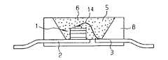
図5に示す実施例が図4に示す実施例と実質的に相異する点は、半導体基体1の自由な表面が直接的にルミネセンス変換エンベローブ5により被われており、このルミネセンス変換エンベローブ5は同じく、更なる透明なエンベローブ10により包囲されていることである。更に、図5に例示されている半導体基体1では、下面コンタクトの代わりに更なるコンタクトが半導体多層構造7上に取り付けられており、この更なるコンタクトは第2のボンディング線ワイヤ14を用いて、所属の電気接続端子2又は3に接続されている。勿論、その種の半導体基体1は他の全ての実施例においても使用可能である。勿論逆に図5の実施例においても、前述の実施例による半導体基体1が使用可能である。 The embodiment shown in FIG. 5 is substantially different from the embodiment shown in FIG. 4 in that the free surface of the
念のため、ここで付言すべきことには勿論、図5の構成形態においても図1の実施例に類似して、一体的なルミネセンス変換エンベローブ5−これは、ルミネセンス外囲器エンベローブ5と更なる透明なエンベローブ10との組合せ結合体にとって代わる−を使用できるということである。 Just in case, it should be noted that, in the configuration of FIG. 5 as well, similar to the embodiment of FIG. 1, an integrated
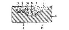
図6の実施例では、ルミネセンス変換層4(上述のような材料)は、直接半導体基体1上に被着されている。この半導体基体1及び電気接続端子2、3はルミネセンス変換層4を通ってもビームの波長変化を生じさせない透明なエンベローブ10により包囲されており、例えば、発光ダイオード技術にて使用可能な透明なエポキシ樹脂又はガラスから作られている。 In the embodiment of FIG. 6, the luminescence conversion layer 4 (material as described above) is deposited directly on the
エンベローブなしで、ルミネセンス変換層4を備えた半導体基体1を勿論、発光ダイオード技術から公知の全てのケーシング構成形態(例えばSMDケーシング、ラジアル(Radial)ケーシング(図5を比較参照のこと))にて有利に使用できる。 Without the envelope, the
図14に示す本発明の半導体発光素子の実施例では、半導体基体1上に透明なウエル部35が配置されており、このウエル部35は半導体基体1上方にウエル36を有する。ウエル部35は透明なエポキシ樹脂又は無機ガラスから成り、そして例えば半導体基体1を含めて電気接続端子2、3の射出成形により作られている。このウエル36内にはルミネセンス変換層4が配置されており、このルミネセンス変換層4は、例えば同じくエポキシ樹脂又は無機ガラスから製造されており、上記の無機の蛍光物質のうち1つからなる粒子37がこれに包含されている。この構成形態の場合、有利には著しく簡単に次のことが確保される。即ち、蛍光物質が半導体基体の作製の際、設定されてない個所、例えば、半導体基体の傍らにて集結することが確保される。勿論、ウエル部分35は別個に作製することもでき、例えばケーシング部分において半導体基体1上方に取り付けることもできる。 In the embodiment of the semiconductor light emitting device of the present invention shown in FIG. 14, a
上述の実施例の全てにおいて、放射された光の色印象の最適化のため及び放射特性の適合化のため、ルミネセンス変換エレメント(ルミネセンス変換エンベロープ5又はルミネセンス変換層4)、場合により透明なエンベロープ15及び/又は場合により更なる透明なエンベローブ10は有利には、いわゆるディフューザ、拡散体を有し得る。その種のディフューザの例は、ミネラル性の充填物質、殊に、CaF2、TiO2、SiO2、CaCO3又はBaSO4又は有機の色素である。これらの材料を簡単に上述のプラスチックに添加することができる。In all of the embodiments described above, a luminescence conversion element (
図7、8及び12には、青色を放射する半導体基体(図7)(λ〜430nmのときルミネセンス最大値)ないしそのような半導体基体を用いて作製された白色発光する本発明の半導体発光素子(図8及び12)の放射スペクトルが示してある。横座標にはそれぞれ波長λが単位nmで、縦座標にはそれぞれ相対的なエレクトロルミネセンス(EL)強度がプロットしてある。 7, 8, and 12 show a semiconductor substrate that emits blue light (FIG. 7) (luminescence maximum value at λ to 430 nm) or the semiconductor light emitting device of the present invention that emits white light produced using such a semiconductor substrate. The emission spectrum of the device (FIGS. 8 and 12) is shown. On the abscissa, the wavelength λ is in unit nm, and on the ordinate, the relative electroluminescence (EL) intensity is plotted.
半導体基体から放射される図7に示すビームうち単に一部のみが比較的長い波長領域に変換され、その結果混合色として白色光が生じる。図8中の破線は、次のような本発明の半導体発光素子からの放射スペクトルを表す。即ち2つの相補的波長領域(青と黄)から成るビーム、ひいては全体の白色光を放射する本発明の半導体発光素子からの放射スペクトルを表す。ここで、放射スペクトルは、ほぼ400nmとほぼ430nmとの間(青)の時、そして、ほぼ550nmとほぼ580との間(黄)の時それぞれ最大値を有する。実線31は、3つの波長領域(加法的色トリオ青、緑、赤)から成る白色を混合する本発明の半導体発光素子の放射スペクトルを表す。ここで、放射スペクトルは例えばほぼ430nm(青)、ほぼ500nm(緑)及びほぼ615nm(赤)の波長の時それぞれ最大値を有する。 Only a part of the beam shown in FIG. 7 radiated from the semiconductor substrate is converted into a relatively long wavelength region, resulting in white light as a mixed color. The broken line in FIG. 8 represents the radiation spectrum from the semiconductor light emitting device of the present invention as follows. That is, it represents a radiation spectrum from the semiconductor light emitting device of the present invention that emits a beam composed of two complementary wavelength regions (blue and yellow), and thus the entire white light. Here, the emission spectrum has a maximum value between about 400 nm and about 430 nm (blue), and between about 550 nm and about 580 (yellow). A
更に、図11中には青色光(ほぼ470nmの波長の時最大値)及び赤色光(ほぼ620nmの波長の時最大値)を放射する本発明の半導体発光素子の放射スペクトルを示す。肉眼にとっての放射された光の全色印象はマゼンタである。半導体基体から放射される放射スペクトルは、同じく図7のそれに相応する。 Further, FIG. 11 shows a radiation spectrum of the semiconductor light emitting device of the present invention that emits blue light (maximum value at a wavelength of approximately 470 nm) and red light (maximum value at a wavelength of approximately 620 nm). The full color impression of emitted light for the naked eye is magenta. The emission spectrum emitted from the semiconductor substrate also corresponds to that of FIG.
図12は、図7の放射スペクトルを放射する半導体基体を備え、蛍光物質としてYAG:Ceが使用されている白色発光する、本発明の半導体発光素子の放射スペクトルを示す。半導体基体から放射される図7のビームのうち単に一部のみが比較的長い波長領域に変換され、その結果色の混合ないし混色として白色光が生じる。図8の種々の破線30から33は、次のような本発明の半導体発光素子の放射スペクトルを示す。即ち、ルミネセンス変換エレメント、本事例ではエポキシ樹脂から成るルミネセンス変換エンベローブが種々のYAG:Ce濃度を有する本発明の半導体発光素子の放射スペクトルを示す。各放射スペクトルはλ=420nmとλ=430nmとの間、即ち青色スペクトル領域において、そしてλ=520nmとλ=545nmとの間、即ち緑色スペクトル領域においてそれぞれ強度最大値を有し、ここで、比較的長い波長の強度最大値を有する放射バンドは大部分黄色スペクトル領域内に位置する。図12のダイヤグラムから明らかなように、本発明の半導体発光素子では簡単にエポキシ樹脂における蛍光物質の濃度の変化により、白色光のCIE色個所を変化させることができる。 FIG. 12 shows the emission spectrum of the semiconductor light emitting device of the present invention, which includes the semiconductor substrate that emits the emission spectrum of FIG. 7 and emits white light using YAG: Ce as the fluorescent material. Only a part of the beam of FIG. 7 emitted from the semiconductor substrate is converted into a relatively long wavelength region, and as a result, white light is generated as a color mixture or color mixture. The various
更にCeドーピングされたガーネット、チオガレート、アルカリ土類硫化物及びアルミン酸塩をベースとする無機の蛍光物質をエポキシ樹脂又はガラス内に分散させずに、これらの蛍光物質を直接半導体基体上に被着することができる。 In addition, inorganic phosphors based on Ce-doped garnet, thiogallate, alkaline earth sulfide and aluminate are deposited directly on the semiconductor substrate without being dispersed in epoxy resin or glass. can do.
上述の無機の蛍光物質の更なる特別な利点とするところは、蛍光物質の濃度が、例えばエポキシ樹脂中で有機の色素におけるとは異なって溶性により制限されないことである。それにより、ルミネセンス変換エレメントの大きな厚さは必要ない。 A further particular advantage of the inorganic phosphors described above is that the concentration of the phosphor is not limited by solubility, as in organic dyes, for example in epoxy resins. Thereby, a large thickness of the luminescence conversion element is not necessary.
上述の実施例に即しての本発明の半導体発光素子の説明は、勿論、この実施例に限定されるものではない。例えば発光ダイオードチップ又はレーザダイオードチップのような半導体基体とは、例えば相応のビームスペクトルを放射するポリマLEDとも解すべきものである。 Of course, the description of the semiconductor light emitting device of the present invention in accordance with the above-described embodiment is not limited to this embodiment. For example, a semiconductor substrate such as a light-emitting diode chip or a laser diode chip should also be understood as a polymer LED emitting a corresponding beam spectrum, for example.
1 半導体基体、 2,3 電気接続端子、 4 ルミネセンス変換層、 5 ルミネセンス変換エンベロープ、 6 蛍光物質、 7 半導体多層構造、 8 基底ケーシング、 9 切欠部、 10,15 透明なエンベロープ DESCRIPTION OF
Claims (19)
Translated fromJapanese前記半導体基体(1)は半導体多層構造(7)を有し、該半導体多層構造(7)は前記半導体発光素子の作動中に、少なくとも青色スペクトル領域又は緑色スペクトル領域から成るビームを包含する第1の波長領域の電磁ビームを放射し、
前記ルミネセンス変換エレメントは、前記第1の波長領域に由来するビームを該第1の波長領域とは異なる第2の波長領域に変換し、前記半導体発光素子は前記第1の波長領域のビーム及び前記第2の波長領域のビームから成る混合ビームを放射し、
前記ルミネセンス変換エレメントは、蛍光物質を包含するシリコン材料から製造されている、ルミネセンス変換エンベロープおよび/またはルミネセンス変換層を有することを特徴とする、半導体発光素子。A semiconductor substrate (1) that emits an electromagnetic beam during operation of the semiconductor light emitting device, at least one first electrical connection terminal (2) and at least one first conductive connection conductively connected to the semiconductor substrate (1) In a semiconductor light emitting device comprising two electrical connection terminals (3) and a luminescence conversion element having at least one fluorescent substance,
The semiconductor substrate (1) has a semiconductor multilayer structure (7), and the semiconductor multilayer structure (7) includes a first beam including at least a blue spectral region or a green spectral region during operation of the semiconductor light emitting device. Emits an electromagnetic beam in the wavelength region of
The luminescence conversion element converts a beam derived from the first wavelength region into a second wavelength region different from the first wavelength region, and the semiconductor light emitting element includes a beam in the first wavelength region and Emitting a mixed beam comprising a beam of said second wavelength region;
The said luminescence conversion element has the luminescence conversion envelope and / or luminescence conversion layer which are manufactured from the silicon material containing a fluorescent substance, The semiconductor light-emitting device characterized by the above-mentioned.
Applications Claiming Priority (2)
| Application Number | Priority Date | Filing Date | Title |
|---|---|---|---|
| DE19625622ADE19625622A1 (en) | 1996-06-26 | 1996-06-26 | Light radiating semiconductor constructional element |
| DE19638667ADE19638667C2 (en) | 1996-09-20 | 1996-09-20 | Mixed-color light-emitting semiconductor component with luminescence conversion element |
Related Parent Applications (1)
| Application Number | Title | Priority Date | Filing Date |
|---|---|---|---|
| JP2003355315ADivisionJP4286104B2 (en) | 1996-06-26 | 2003-10-15 | Semiconductor light emitting device and use of semiconductor light emitting device |
Publications (2)
| Publication Number | Publication Date |
|---|---|
| JP2005252293Atrue JP2005252293A (en) | 2005-09-15 |
| JP4334497B2 JP4334497B2 (en) | 2009-09-30 |
Family
ID=26026958
Family Applications (10)
| Application Number | Title | Priority Date | Filing Date |
|---|---|---|---|
| JP50211798AExpired - LifetimeJP3773541B2 (en) | 1996-06-26 | 1997-06-26 | Semiconductor light emitting device having luminescence conversion element |
| JP2003355316AExpired - LifetimeJP4280598B2 (en) | 1996-06-26 | 2003-10-15 | Light emitting semiconductor chip |
| JP2003355315AExpired - LifetimeJP4286104B2 (en) | 1996-06-26 | 2003-10-15 | Semiconductor light emitting device and use of semiconductor light emitting device |
| JP2003355314AExpired - LifetimeJP4278479B2 (en) | 1996-06-26 | 2003-10-15 | Semiconductor light emitting device |
| JP2003355317AExpired - LifetimeJP4308620B2 (en) | 1996-06-26 | 2003-10-15 | A separately manufactured coated plate mounted on a casing of a semiconductor light emitting device |
| JP2005112811AExpired - LifetimeJP4001893B2 (en) | 1996-06-26 | 2005-04-08 | Semiconductor light emitting device |
| JP2005112809AExpired - LifetimeJP4334497B2 (en) | 1996-06-26 | 2005-04-08 | Semiconductor light emitting device |
| JP2005112810AExpired - LifetimeJP4001892B2 (en) | 1996-06-26 | 2005-04-08 | Semiconductor light emitting element, LED display device, illumination device, and illumination device for liquid crystal display unit |
| JP2006268658AExpired - LifetimeJP4388940B2 (en) | 1996-06-26 | 2006-09-29 | Light emitting semiconductor chip |
| JP2007264556AExpired - LifetimeJP5260018B2 (en) | 1996-06-26 | 2007-10-10 | Semiconductor element |
Family Applications Before (6)
| Application Number | Title | Priority Date | Filing Date |
|---|---|---|---|
| JP50211798AExpired - LifetimeJP3773541B2 (en) | 1996-06-26 | 1997-06-26 | Semiconductor light emitting device having luminescence conversion element |
| JP2003355316AExpired - LifetimeJP4280598B2 (en) | 1996-06-26 | 2003-10-15 | Light emitting semiconductor chip |
| JP2003355315AExpired - LifetimeJP4286104B2 (en) | 1996-06-26 | 2003-10-15 | Semiconductor light emitting device and use of semiconductor light emitting device |
| JP2003355314AExpired - LifetimeJP4278479B2 (en) | 1996-06-26 | 2003-10-15 | Semiconductor light emitting device |
| JP2003355317AExpired - LifetimeJP4308620B2 (en) | 1996-06-26 | 2003-10-15 | A separately manufactured coated plate mounted on a casing of a semiconductor light emitting device |
| JP2005112811AExpired - LifetimeJP4001893B2 (en) | 1996-06-26 | 2005-04-08 | Semiconductor light emitting device |
Family Applications After (3)
| Application Number | Title | Priority Date | Filing Date |
|---|---|---|---|
| JP2005112810AExpired - LifetimeJP4001892B2 (en) | 1996-06-26 | 2005-04-08 | Semiconductor light emitting element, LED display device, illumination device, and illumination device for liquid crystal display unit |
| JP2006268658AExpired - LifetimeJP4388940B2 (en) | 1996-06-26 | 2006-09-29 | Light emitting semiconductor chip |
| JP2007264556AExpired - LifetimeJP5260018B2 (en) | 1996-06-26 | 2007-10-10 | Semiconductor element |
Country Status (8)
| Country | Link |
|---|---|
| US (10) | US7078732B1 (en) |
| EP (12) | EP1441397B1 (en) |
| JP (10) | JP3773541B2 (en) |
| KR (11) | KR100537349B1 (en) |
| CN (3) | CN1534802B (en) |
| BR (2) | BR9709998B1 (en) |
| DE (6) | DE59711671D1 (en) |
| WO (1) | WO1997050132A1 (en) |
Cited By (2)
| Publication number | Priority date | Publication date | Assignee | Title |
|---|---|---|---|---|
| JP2012054606A (en)* | 2006-12-15 | 2012-03-15 | Cree Inc | Reflective mount substrate for light emitting diode |
| TWI420227B (en)* | 2005-10-04 | 2013-12-21 | Koninkl Philips Electronics Nv | A laser projection system based on a luminescent screen |
Families Citing this family (771)
| Publication number | Priority date | Publication date | Assignee | Title |
|---|---|---|---|---|
| US6600175B1 (en) | 1996-03-26 | 2003-07-29 | Advanced Technology Materials, Inc. | Solid state white light emitter and display using same |
| US20040239243A1 (en)* | 1996-06-13 | 2004-12-02 | Roberts John K. | Light emitting assembly |
| KR100537349B1 (en) | 1996-06-26 | 2006-02-28 | 오스람 게젤샤프트 미트 베쉬랭크터 하프퉁 | Light-emitting semiconductor component with luminescence conversion element |
| DE19638667C2 (en) | 1996-09-20 | 2001-05-17 | Osram Opto Semiconductors Gmbh | Mixed-color light-emitting semiconductor component with luminescence conversion element |
| AU744210B2 (en)* | 1996-07-29 | 2002-02-21 | Nichia Corporation | Light emitting device and display |
| TW383508B (en)* | 1996-07-29 | 2000-03-01 | Nichia Kagaku Kogyo Kk | Light emitting device and display |
| DE19645035C1 (en)* | 1996-10-31 | 1998-04-30 | Siemens Ag | Multi-color light emitting image display device |
| US5895932A (en)* | 1997-01-24 | 1999-04-20 | International Business Machines Corporation | Hybrid organic-inorganic semiconductor light emitting diodes |
| JP3378465B2 (en)* | 1997-05-16 | 2003-02-17 | 株式会社東芝 | Light emitting device |
| EP0883195A1 (en)* | 1997-06-03 | 1998-12-09 | BARR & STROUD LIMITED | Head tracking system comprising LED with fluorescent coating |
| JP4271747B2 (en)* | 1997-07-07 | 2009-06-03 | 株式会社朝日ラバー | Translucent coating material for light emitting diode and fluorescent color light source |
| US6319425B1 (en) | 1997-07-07 | 2001-11-20 | Asahi Rubber Inc. | Transparent coating member for light-emitting diodes and a fluorescent color light source |
| US6623670B2 (en) | 1997-07-07 | 2003-09-23 | Asahi Rubber Inc. | Method of molding a transparent coating member for light-emitting diodes |
| US5847507A (en)* | 1997-07-14 | 1998-12-08 | Hewlett-Packard Company | Fluorescent dye added to epoxy of light emitting diode lens |
| CN1142598C (en) | 1997-07-25 | 2004-03-17 | 日亚化学工业株式会社 | Nitride semiconductor light emitting device |
| US7038398B1 (en) | 1997-08-26 | 2006-05-02 | Color Kinetics, Incorporated | Kinetic illumination system and methods |
| US7161313B2 (en)* | 1997-08-26 | 2007-01-09 | Color Kinetics Incorporated | Light emitting diode based products |
| US6806659B1 (en) | 1997-08-26 | 2004-10-19 | Color Kinetics, Incorporated | Multicolored LED lighting method and apparatus |
| US20030133292A1 (en)* | 1999-11-18 | 2003-07-17 | Mueller George G. | Methods and apparatus for generating and modulating white light illumination conditions |
| US7014336B1 (en) | 1999-11-18 | 2006-03-21 | Color Kinetics Incorporated | Systems and methods for generating and modulating illumination conditions |
| US6340824B1 (en)* | 1997-09-01 | 2002-01-22 | Kabushiki Kaisha Toshiba | Semiconductor light emitting device including a fluorescent material |
| DE19755734A1 (en)* | 1997-12-15 | 1999-06-24 | Siemens Ag | Method for producing a surface-mountable optoelectronic component |
| US7598686B2 (en) | 1997-12-17 | 2009-10-06 | Philips Solid-State Lighting Solutions, Inc. | Organic light emitting diode methods and apparatus |
| US6252254B1 (en) | 1998-02-06 | 2001-06-26 | General Electric Company | Light emitting device with phosphor composition |
| US6580097B1 (en)* | 1998-02-06 | 2003-06-17 | General Electric Company | Light emitting device with phosphor composition |
| US6152590A (en) | 1998-02-13 | 2000-11-28 | Donnelly Hohe Gmbh & Co. Kg | Lighting device for motor vehicles |
| US6501091B1 (en)* | 1998-04-01 | 2002-12-31 | Massachusetts Institute Of Technology | Quantum dot white and colored light emitting diodes |
| FR2779694B1 (en)* | 1998-06-10 | 2000-08-11 | Sagem | POLYCHROME LIGHTED DASHBOARD |
| US5959316A (en)* | 1998-09-01 | 1999-09-28 | Hewlett-Packard Company | Multiple encapsulation of phosphor-LED devices |
| KR100702273B1 (en)† | 1998-09-28 | 2007-03-30 | 코닌클리즈케 필립스 일렉트로닉스 엔.브이. | Lighting system |
| US6429583B1 (en) | 1998-11-30 | 2002-08-06 | General Electric Company | Light emitting device with ba2mgsi2o7:eu2+, ba2sio4:eu2+, or (srxcay ba1-x-y)(a1zga1-z)2sr:eu2+phosphors |
| JP2000208822A (en) | 1999-01-11 | 2000-07-28 | Matsushita Electronics Industry Corp | Semiconductor light emitting device |
| DE19902750A1 (en) | 1999-01-25 | 2000-08-03 | Osram Opto Semiconductors Gmbh | Semiconductor component for generating mixed-colored electromagnetic radiation |
| US6683325B2 (en)* | 1999-01-26 | 2004-01-27 | Patent-Treuhand-Gesellschaft-für Elektrische Glühlampen mbH | Thermal expansion compensated opto-electronic semiconductor element, particularly ultraviolet (UV) light emitting diode, and method of its manufacture |
| JP2000223749A (en)* | 1999-01-29 | 2000-08-11 | Seiwa Electric Mfg Co Ltd | Light emitting diode lamp, method for manufacturing the same, chip type light emitting diode element and dot matrix type light emitting diode unit |
| JP3770014B2 (en) | 1999-02-09 | 2006-04-26 | 日亜化学工業株式会社 | Nitride semiconductor device |
| US6351069B1 (en)* | 1999-02-18 | 2002-02-26 | Lumileds Lighting, U.S., Llc | Red-deficiency-compensating phosphor LED |
| ATE452445T1 (en) | 1999-03-04 | 2010-01-15 | Nichia Corp | NITRIDE SEMICONDUCTOR LASER ELEMENT |
| US6528234B1 (en)* | 1999-03-05 | 2003-03-04 | The United States Of America As Represented By The Secretary Of The Navy | II-VI compounds as a medium for optical data storage through fast persistent high density spectral holeburning |
| US6514435B1 (en)* | 1999-03-05 | 2003-02-04 | The United States Of America As Represented By The Secretary Of The Navy | High density and fast persistent spectral holeburning in II-VI compounds for optical data storage |
| DE19922361C2 (en) | 1999-05-14 | 2003-05-28 | Osram Opto Semiconductors Gmbh | LED module for display devices |
| US6489637B1 (en)* | 1999-06-09 | 2002-12-03 | Sanyo Electric Co., Ltd. | Hybrid integrated circuit device |
| EP1116419B1 (en) | 1999-07-23 | 2004-10-06 | Osram Opto Semiconductors GmbH | Luminescent array, wavelength-converting sealing material and light source |
| WO2001008452A1 (en) | 1999-07-23 | 2001-02-01 | Patent-Treuhand-Gesellschaft für elektrische Glühlampen mbH | Luminous substance for a light source and light source associated therewith |
| DE29914037U1 (en)* | 1999-08-11 | 2000-12-28 | Diehl AKO Stiftung GmbH & Co. KG, 88239 Wangen | Indoor lighting for household appliances |
| US6504301B1 (en)* | 1999-09-03 | 2003-01-07 | Lumileds Lighting, U.S., Llc | Non-incandescent lightbulb package using light emitting diodes |
| US6696703B2 (en) | 1999-09-27 | 2004-02-24 | Lumileds Lighting U.S., Llc | Thin film phosphor-converted light emitting diode device |
| KR100683364B1 (en) | 1999-09-27 | 2007-02-15 | 필립스 루미리즈 라이팅 캄파니 엘엘씨 | Light Emitting Diodes Generate White Light by Complete Fluorescence Conversion |
| US6686691B1 (en) | 1999-09-27 | 2004-02-03 | Lumileds Lighting, U.S., Llc | Tri-color, white light LED lamps |
| US20020176259A1 (en) | 1999-11-18 | 2002-11-28 | Ducharme Alfred D. | Systems and methods for converting illumination |
| US7202506B1 (en) | 1999-11-19 | 2007-04-10 | Cree, Inc. | Multi element, multi color solid state LED/laser |
| US8829546B2 (en) | 1999-11-19 | 2014-09-09 | Cree, Inc. | Rare earth doped layer or substrate for light conversion |
| US6513949B1 (en) | 1999-12-02 | 2003-02-04 | Koninklijke Philips Electronics N.V. | LED/phosphor-LED hybrid lighting systems |
| DE19963805B4 (en) | 1999-12-30 | 2005-01-27 | Osram Opto Semiconductors Gmbh | White light source based on non-linear optical processes |
| DE19964252A1 (en) | 1999-12-30 | 2002-06-06 | Osram Opto Semiconductors Gmbh | Surface mount component for an LED white light source |
| DE10010638A1 (en)* | 2000-03-03 | 2001-09-13 | Osram Opto Semiconductors Gmbh | Making light emitting semiconducting body with luminescence conversion element involves applying suspension with solvent, adhesive, luminescent material |
| US6522065B1 (en)* | 2000-03-27 | 2003-02-18 | General Electric Company | Single phosphor for creating white light with high luminosity and high CRI in a UV led device |
| US6867542B1 (en)* | 2000-03-29 | 2005-03-15 | General Electric Company | Floating chip photonic device and method of manufacture |
| US6603258B1 (en)* | 2000-04-24 | 2003-08-05 | Lumileds Lighting, U.S. Llc | Light emitting diode device that emits white light |
| DE10020465A1 (en) | 2000-04-26 | 2001-11-08 | Osram Opto Semiconductors Gmbh | Radiation-emitting semiconductor component with luminescence conversion element |
| DE10023353A1 (en)* | 2000-05-12 | 2001-11-29 | Osram Opto Semiconductors Gmbh | Optoelectronic component and method for producing it |
| US6501100B1 (en)* | 2000-05-15 | 2002-12-31 | General Electric Company | White light emitting phosphor blend for LED devices |
| JP4066620B2 (en)* | 2000-07-21 | 2008-03-26 | 日亜化学工業株式会社 | LIGHT EMITTING ELEMENT, DISPLAY DEVICE HAVING LIGHT EMITTING ELEMENT AND METHOD FOR MANUFACTURING DISPLAY DEVICE |
| JP2002050797A (en) | 2000-07-31 | 2002-02-15 | Toshiba Corp | Semiconductor-excited phosphor light emitting device and method of manufacturing the same |
| JP2002141556A (en) | 2000-09-12 | 2002-05-17 | Lumileds Lighting Us Llc | Light-emitting diode with improved light extraction effect |
| JP3609709B2 (en)* | 2000-09-29 | 2005-01-12 | 株式会社シチズン電子 | Light emitting diode |
| US6650044B1 (en)* | 2000-10-13 | 2003-11-18 | Lumileds Lighting U.S., Llc | Stenciling phosphor layers on light emitting diodes |
| JP3614776B2 (en)* | 2000-12-19 | 2005-01-26 | シャープ株式会社 | Chip component type LED and its manufacturing method |
| US6800870B2 (en)* | 2000-12-20 | 2004-10-05 | Michel Sayag | Light stimulating and collecting methods and apparatus for storage-phosphor image plates |
| US20020079505A1 (en)* | 2000-12-21 | 2002-06-27 | Stefan Becker | Semiconductor light unit and method for production of the same |
| JP2002195858A (en)* | 2000-12-27 | 2002-07-10 | Nippon Seiki Co Ltd | Display |
| DE10065381B4 (en)* | 2000-12-27 | 2010-08-26 | Osram Opto Semiconductors Gmbh | Radiation-emitting semiconductor component with luminescence conversion element |
| AT410266B (en) | 2000-12-28 | 2003-03-25 | Tridonic Optoelectronics Gmbh | LIGHT SOURCE WITH A LIGHT-EMITTING ELEMENT |
| US6930737B2 (en)* | 2001-01-16 | 2005-08-16 | Visteon Global Technologies, Inc. | LED backlighting system |
| MY145695A (en) | 2001-01-24 | 2012-03-30 | Nichia Corp | Light emitting diode, optical semiconductor device, epoxy resin composition suited for optical semiconductor device, and method for manufacturing the same |
| JP2002232013A (en)* | 2001-02-02 | 2002-08-16 | Rohm Co Ltd | Semiconductor light emitting device |
| DE10105802A1 (en) | 2001-02-07 | 2002-08-08 | Patent Treuhand Ges Fuer Elektrische Gluehlampen Mbh | Semiconductor component with reflector |
| DE10109349B4 (en)* | 2001-02-27 | 2012-04-19 | Osram Opto Semiconductors Gmbh | Radiation-emitting semiconductor component |
| US6417019B1 (en)* | 2001-04-04 | 2002-07-09 | Lumileds Lighting, U.S., Llc | Phosphor converted light emitting diode |
| US6949771B2 (en)* | 2001-04-25 | 2005-09-27 | Agilent Technologies, Inc. | Light source |
| US6598998B2 (en)* | 2001-05-04 | 2003-07-29 | Lumileds Lighting, U.S., Llc | Side emitting light emitting device |
| US6989412B2 (en) | 2001-06-06 | 2006-01-24 | Henkel Corporation | Epoxy molding compounds containing phosphor and process for preparing such compositions |
| US6576488B2 (en) | 2001-06-11 | 2003-06-10 | Lumileds Lighting U.S., Llc | Using electrophoresis to produce a conformally coated phosphor-converted light emitting semiconductor |
| US6642652B2 (en) | 2001-06-11 | 2003-11-04 | Lumileds Lighting U.S., Llc | Phosphor-converted light emitting device |
| JP4789350B2 (en)* | 2001-06-11 | 2011-10-12 | シチズン電子株式会社 | Manufacturing method of light emitting diode |
| US6664560B2 (en)* | 2001-06-15 | 2003-12-16 | Cree, Inc. | Ultraviolet light emitting diode |
| DE10131698A1 (en)* | 2001-06-29 | 2003-01-30 | Osram Opto Semiconductors Gmbh | Surface-mountable radiation-emitting component and method for its production |
| TW552726B (en)* | 2001-07-26 | 2003-09-11 | Matsushita Electric Works Ltd | Light emitting device in use of LED |
| DE10137641A1 (en)* | 2001-08-03 | 2003-02-20 | Osram Opto Semiconductors Gmbh | Hybrid LED |
| JP3948650B2 (en) | 2001-10-09 | 2007-07-25 | アバゴ・テクノロジーズ・イーシービーユー・アイピー(シンガポール)プライベート・リミテッド | Light emitting diode and manufacturing method thereof |
| DE10153259A1 (en)* | 2001-10-31 | 2003-05-22 | Osram Opto Semiconductors Gmbh | Optoelectronic component |
| JP2003152227A (en)* | 2001-11-14 | 2003-05-23 | Citizen Electronics Co Ltd | LED color correction means and color correction method |
| JP3768864B2 (en)* | 2001-11-26 | 2006-04-19 | シチズン電子株式会社 | Surface mount type light emitting diode and manufacturing method thereof |
| US6836502B2 (en) | 2002-01-17 | 2004-12-28 | Hutchinson Technology Incorporated | Spectroscopy light source |
| US6734466B2 (en)* | 2002-03-05 | 2004-05-11 | Agilent Technologies, Inc. | Coated phosphor filler and a method of forming the coated phosphor filler |
| US6943379B2 (en)* | 2002-04-04 | 2005-09-13 | Toyoda Gosei Co., Ltd. | Light emitting diode |
| KR100632659B1 (en)* | 2002-05-31 | 2006-10-11 | 서울반도체 주식회사 | White light emitting diode |
| CA2489237A1 (en)* | 2002-06-13 | 2003-12-24 | Cree, Inc. | Semiconductor emitter comprising a saturated phosphor |
| US6841802B2 (en) | 2002-06-26 | 2005-01-11 | Oriol, Inc. | Thin film light emitting diode |
| US7088040B1 (en)* | 2002-06-27 | 2006-08-08 | University Of Central Florida Research Foundation, Inc. | Light source using emitting particles to provide visible light |
| KR101030068B1 (en)* | 2002-07-08 | 2011-04-19 | 니치아 카가쿠 고교 가부시키가이샤 | Nitride semiconductor device manufacturing method and nitride semiconductor device |
| JP2004047748A (en)* | 2002-07-12 | 2004-02-12 | Stanley Electric Co Ltd | Light emitting diode |
| US7928455B2 (en)* | 2002-07-15 | 2011-04-19 | Epistar Corporation | Semiconductor light-emitting device and method for forming the same |
| WO2004017407A1 (en) | 2002-07-31 | 2004-02-26 | Osram Opto Semiconductors Gmbh | Surface-mounted semiconductor component and method for the production thereof |
| JP4360788B2 (en)* | 2002-08-29 | 2009-11-11 | シチズン電子株式会社 | Backlight for liquid crystal display panel and method of manufacturing light emitting diode used therefor |
| US7800121B2 (en) | 2002-08-30 | 2010-09-21 | Lumination Llc | Light emitting diode component |
| CN100468791C (en)* | 2002-08-30 | 2009-03-11 | 吉尔科有限公司 | Light emitting diode with improved effience |
| US7224000B2 (en)* | 2002-08-30 | 2007-05-29 | Lumination, Llc | Light emitting diode component |
| US10340424B2 (en) | 2002-08-30 | 2019-07-02 | GE Lighting Solutions, LLC | Light emitting diode component |
| US20050218781A1 (en)* | 2002-09-09 | 2005-10-06 | Hsing Chen | Triple wavelengths light emitting diode |
| JP4201167B2 (en)* | 2002-09-26 | 2008-12-24 | シチズン電子株式会社 | Manufacturing method of white light emitting device |
| US6822991B2 (en)* | 2002-09-30 | 2004-11-23 | Lumileds Lighting U.S., Llc | Light emitting devices including tunnel junctions |
| US7592636B2 (en)* | 2002-09-30 | 2009-09-22 | Osram Opto Semiconductors Gmbh | Radiation-emitting semiconductor component and method for the production thereof |
| JP2004128273A (en) | 2002-10-03 | 2004-04-22 | Sharp Corp | Light emitting element |
| JP4280050B2 (en) | 2002-10-07 | 2009-06-17 | シチズン電子株式会社 | White light emitting device |
| AU2003278009A1 (en)* | 2002-10-18 | 2004-05-04 | Ifire Technology Inc. | Color electroluminescent displays |
| US20060003477A1 (en) | 2002-10-30 | 2006-01-05 | Bert Braune | Method for producing a light source provided with electroluminescent diodes and comprising a luminescence conversion element |
| DE10258193B4 (en)* | 2002-12-12 | 2014-04-10 | Osram Opto Semiconductors Gmbh | Method for producing light-emitting diode light sources with luminescence conversion element |
| WO2004059750A1 (en)* | 2002-12-25 | 2004-07-15 | Japan Science And Technology Agency | Light emitting element device, light receiving element device, optical apparatus, fluoride crystal, process for producing fluoride crystal and crucible |
| DE10261428B8 (en)* | 2002-12-30 | 2012-09-20 | Osram Opto Semiconductors Gmbh | Radiation-emitting semiconductor component with multiple luminescence conversion elements |
| DE10261672B4 (en)* | 2002-12-31 | 2005-11-24 | Osram Opto Semiconductors Gmbh | LED chip with conversion substance, optoelectronic component with such an LED chip and method for producing such an LED chip |
| TWI351548B (en) | 2003-01-15 | 2011-11-01 | Semiconductor Energy Lab | Manufacturing method of liquid crystal display dev |
| US7042020B2 (en) | 2003-02-14 | 2006-05-09 | Cree, Inc. | Light emitting device incorporating a luminescent material |
| US7423296B2 (en)* | 2003-02-26 | 2008-09-09 | Avago Technologies Ecbu Ip Pte Ltd | Apparatus for producing a spectrally-shifted light output from a light emitting device utilizing thin-film luminescent layers |
| KR20050113200A (en)* | 2003-02-26 | 2005-12-01 | 크리, 인코포레이티드 | Composite white light source and method for fabricating |
| JP4131178B2 (en)* | 2003-02-28 | 2008-08-13 | 豊田合成株式会社 | Light emitting device |
| DE10308866A1 (en) | 2003-02-28 | 2004-09-09 | Osram Opto Semiconductors Gmbh | Lighting module and method for its production |
| US20040173808A1 (en)* | 2003-03-07 | 2004-09-09 | Bor-Jen Wu | Flip-chip like light emitting device package |
| CN101789482B (en)* | 2003-03-10 | 2013-04-17 | 丰田合成株式会社 | Solid element device and method for manufacture thereof |
| US7038370B2 (en)* | 2003-03-17 | 2006-05-02 | Lumileds Lighting, U.S., Llc | Phosphor converted light emitting device |
| US7279832B2 (en)* | 2003-04-01 | 2007-10-09 | Innovalight, Inc. | Phosphor materials and illumination devices made therefrom |
| US20040252488A1 (en)* | 2003-04-01 | 2004-12-16 | Innovalight | Light-emitting ceiling tile |
| DE10316769A1 (en)* | 2003-04-10 | 2004-10-28 | Patent-Treuhand-Gesellschaft für elektrische Glühlampen mbH | Luminescence conversion LED used in optical semiconductor components has LED chip emitting primary radiation in specified region which is partially or completely converted into longer wavelength radiation |
| JP3931916B2 (en)* | 2003-04-24 | 2007-06-20 | 日亜化学工業株式会社 | Semiconductor device and manufacturing method thereof |
| CA2523544A1 (en)* | 2003-04-30 | 2004-11-18 | Cree, Inc. | High powered light emitter packages with compact optics |
| US7005679B2 (en) | 2003-05-01 | 2006-02-28 | Cree, Inc. | Multiple component solid state white light |
| US7777235B2 (en) | 2003-05-05 | 2010-08-17 | Lighting Science Group Corporation | Light emitting diodes with improved light collimation |
| US7157745B2 (en) | 2004-04-09 | 2007-01-02 | Blonder Greg E | Illumination devices comprising white light emitting diodes and diode arrays and method and apparatus for making them |
| US7633093B2 (en) | 2003-05-05 | 2009-12-15 | Lighting Science Group Corporation | Method of making optical light engines with elevated LEDs and resulting product |
| US7528421B2 (en) | 2003-05-05 | 2009-05-05 | Lamina Lighting, Inc. | Surface mountable light emitting diode assemblies packaged for high temperature operation |
| US7040774B2 (en)* | 2003-05-23 | 2006-05-09 | Goldeneye, Inc. | Illumination systems utilizing multiple wavelength light recycling |
| JP4138586B2 (en)* | 2003-06-13 | 2008-08-27 | スタンレー電気株式会社 | LED lamp for light source and vehicle headlamp using the same |
| CN100511732C (en) | 2003-06-18 | 2009-07-08 | 丰田合成株式会社 | Light emitting device |
| AT412928B (en)* | 2003-06-18 | 2005-08-25 | Guenther Dipl Ing Dr Leising | METHOD FOR PRODUCING A WHITE LED AND WHITE LED LIGHT SOURCE |
| JP4024721B2 (en)* | 2003-06-20 | 2007-12-19 | 株式会社小糸製作所 | Vehicle lamp and light source module |
| US7521667B2 (en) | 2003-06-23 | 2009-04-21 | Advanced Optical Technologies, Llc | Intelligent solid state lighting |
| US7145125B2 (en) | 2003-06-23 | 2006-12-05 | Advanced Optical Technologies, Llc | Integrating chamber cone light using LED sources |
| JP2005026688A (en)* | 2003-06-30 | 2005-01-27 | Osram Opto Semiconductors Gmbh | Radiation emitting semiconductor chip, method for manufacturing the semiconductor chip, and method for adjusting and setting the brightness of the semiconductor chip |
| US8999736B2 (en)* | 2003-07-04 | 2015-04-07 | Epistar Corporation | Optoelectronic system |
| US20050006659A1 (en)* | 2003-07-09 | 2005-01-13 | Ng Kee Yean | Light emitting diode utilizing a discrete wavelength-converting layer for color conversion |
| JP4200849B2 (en)* | 2003-07-17 | 2008-12-24 | 日産自動車株式会社 | Infrared projector for vehicles |
| DE102004034166B4 (en)* | 2003-07-17 | 2015-08-20 | Toyoda Gosei Co., Ltd. | Light-emitting device |
| JP4238666B2 (en)* | 2003-07-17 | 2009-03-18 | 豊田合成株式会社 | Method for manufacturing light emitting device |
| JP2005064233A (en)* | 2003-08-12 | 2005-03-10 | Stanley Electric Co Ltd | Wavelength conversion type LED |
| EP1659335A4 (en)* | 2003-08-28 | 2010-05-05 | Mitsubishi Chem Corp | LIGHT EMITTING DEVICE AND PHOSPHORUS |
| EP1515368B1 (en)* | 2003-09-05 | 2019-12-25 | Nichia Corporation | Light equipment |
| US7029935B2 (en)* | 2003-09-09 | 2006-04-18 | Cree, Inc. | Transmissive optical elements including transparent plastic shell having a phosphor dispersed therein, and methods of fabricating same |
| JP4140042B2 (en)* | 2003-09-17 | 2008-08-27 | スタンレー電気株式会社 | LED light source device using phosphor and vehicle headlamp using LED light source device |
| JP2005093712A (en)* | 2003-09-17 | 2005-04-07 | Stanley Electric Co Ltd | Semiconductor light emitting device |
| US7915085B2 (en) | 2003-09-18 | 2011-03-29 | Cree, Inc. | Molded chip fabrication method |
| JP4402425B2 (en)* | 2003-10-24 | 2010-01-20 | スタンレー電気株式会社 | Vehicle headlamp |
| US6933535B2 (en)* | 2003-10-31 | 2005-08-23 | Lumileds Lighting U.S., Llc | Light emitting devices with enhanced luminous efficiency |
| DE10351397A1 (en)* | 2003-10-31 | 2005-06-16 | Osram Opto Semiconductors Gmbh | LED chip |
| DE10351349A1 (en)* | 2003-10-31 | 2005-06-16 | Osram Opto Semiconductors Gmbh | Production of a luminescent diode chip applies a radiation decoupling surface and a semiconductor body with an epitaxial-grown sequence of semiconductor layers with an active zone |
| US20050099808A1 (en)* | 2003-11-12 | 2005-05-12 | Cheng Tzu C. | Light-emitting device |
| CN100377370C (en)* | 2003-11-22 | 2008-03-26 | 鸿富锦精密工业(深圳)有限公司 | Light-emitting diode and surface light source device |
| JP4385741B2 (en)* | 2003-11-25 | 2009-12-16 | パナソニック電工株式会社 | Light emitting device |
| US7518158B2 (en) | 2003-12-09 | 2009-04-14 | Cree, Inc. | Semiconductor light emitting devices and submounts |
| JP2005191420A (en)* | 2003-12-26 | 2005-07-14 | Stanley Electric Co Ltd | Semiconductor light emitting device having wavelength conversion layer and manufacturing method thereof |
| DE10361650A1 (en)* | 2003-12-30 | 2005-08-04 | Osram Opto Semiconductors Gmbh | Optoelectronic module and method for its production |
| JP2005197329A (en)* | 2004-01-05 | 2005-07-21 | Stanley Electric Co Ltd | Surface mount semiconductor device and lead frame structure thereof |
| US7183588B2 (en)* | 2004-01-08 | 2007-02-27 | Avago Technologies Ecbu Ip (Singapore) Pte. Ltd. | Light emission device |
| DE102004003928B4 (en)* | 2004-01-26 | 2012-02-23 | Tay Kheng Chiong | A miniaturized SM-technology optoelectronic device and method of making this device |
| US7250715B2 (en)* | 2004-02-23 | 2007-07-31 | Philips Lumileds Lighting Company, Llc | Wavelength converted semiconductor light emitting devices |
| DE102004029412A1 (en)* | 2004-02-27 | 2005-10-13 | Osram Opto Semiconductors Gmbh | Radiation-emitting semiconductor chip and method for producing such a semiconductor chip |
| JP2005244075A (en)* | 2004-02-27 | 2005-09-08 | Matsushita Electric Works Ltd | Light emitting device |
| JP2005286312A (en) | 2004-03-02 | 2005-10-13 | Fujikura Ltd | LIGHT EMITTING DEVICE AND LIGHTING DEVICE |
| US7573072B2 (en)* | 2004-03-10 | 2009-08-11 | Lumination Llc | Phosphor and blends thereof for use in LEDs |
| US7239080B2 (en)* | 2004-03-11 | 2007-07-03 | Avago Technologies Ecbu Ip (Singapore) Pte. Ltd | LED display with overlay |
| KR20050092300A (en)* | 2004-03-15 | 2005-09-21 | 삼성전기주식회사 | High power led package |
| US20050199990A1 (en)* | 2004-03-15 | 2005-09-15 | Intersil Americas Inc. | Protection of plastic detector's packages against shortwave light destruction |
| DE102004013680A1 (en)* | 2004-03-18 | 2005-10-20 | Siemens Ag | Light source for imaging unit |
| JP4504056B2 (en) | 2004-03-22 | 2010-07-14 | スタンレー電気株式会社 | Manufacturing method of semiconductor light emitting device |
| TWI286393B (en)* | 2004-03-24 | 2007-09-01 | Toshiba Lighting & Technology | Lighting apparatus |
| JP2005285925A (en)* | 2004-03-29 | 2005-10-13 | Stanley Electric Co Ltd | LED |
| DE102005014144A1 (en)* | 2004-03-29 | 2005-11-24 | Stanley Electric Co. Ltd. | led |
| JP2005285920A (en)* | 2004-03-29 | 2005-10-13 | Stanley Electric Co Ltd | LED |
| US7497581B2 (en)* | 2004-03-30 | 2009-03-03 | Goldeneye, Inc. | Light recycling illumination systems with wavelength conversion |
| JP4229447B2 (en)* | 2004-03-31 | 2009-02-25 | スタンレー電気株式会社 | Semiconductor light emitting device and manufacturing method |
| US7517728B2 (en)* | 2004-03-31 | 2009-04-14 | Cree, Inc. | Semiconductor light emitting devices including a luminescent conversion element |
| US7326583B2 (en)* | 2004-03-31 | 2008-02-05 | Cree, Inc. | Methods for packaging of a semiconductor light emitting device |
| US7279346B2 (en)* | 2004-03-31 | 2007-10-09 | Cree, Inc. | Method for packaging a light emitting device by one dispense then cure step followed by another |
| JP5013405B2 (en)* | 2004-03-31 | 2012-08-29 | 日本電気硝子株式会社 | Phosphor and light emitting diode |
| US7868343B2 (en)* | 2004-04-06 | 2011-01-11 | Cree, Inc. | Light-emitting devices having multiple encapsulation layers with at least one of the encapsulation layers including nanoparticles and methods of forming the same |
| WO2005104247A1 (en)* | 2004-04-19 | 2005-11-03 | Matsushita Electric Industrial Co., Ltd. | Method for fabricating led illumination light source and led illumination light source |
| JP4471356B2 (en)* | 2004-04-23 | 2010-06-02 | スタンレー電気株式会社 | Semiconductor light emitting device |
| EP1753035A4 (en)* | 2004-04-28 | 2011-12-21 | Panasonic Corp | LIGHT EMITTING DEVICE AND METHOD OF MANUFACTURING THE SAME |
| AU2005240186B2 (en)* | 2004-05-05 | 2011-02-03 | Rensselaer Polytechnic Institute | High efficiency light source using solid-state emitter and down-conversion material |
| US7837348B2 (en) | 2004-05-05 | 2010-11-23 | Rensselaer Polytechnic Institute | Lighting system using multiple colored light emitting sources and diffuser element |
| TWI242893B (en)* | 2004-05-07 | 2005-11-01 | Lite On Technology Corp | White light-emitting apparatus |
| US11158768B2 (en) | 2004-05-07 | 2021-10-26 | Bruce H. Baretz | Vacuum light emitting diode |
| US11355676B2 (en) | 2004-05-07 | 2022-06-07 | Bruce H. Baretz | Light emitting diode |
| JP4632690B2 (en)* | 2004-05-11 | 2011-02-16 | スタンレー電気株式会社 | Semiconductor light emitting device and manufacturing method thereof |
| JP3994094B2 (en)* | 2004-05-27 | 2007-10-17 | ローム株式会社 | Light emitting diode lamp |
| JP5366399B2 (en) | 2004-05-31 | 2013-12-11 | オスラム オプト セミコンダクターズ ゲゼルシャフト ミット ベシュレンクテル ハフツング | Optoelectronic semiconductor component and casing substrate for the component |
| DE102004040468B4 (en)* | 2004-05-31 | 2022-02-03 | OSRAM Opto Semiconductors Gesellschaft mit beschränkter Haftung | Optoelectronic semiconductor component and housing base body for such a component |
| US7553683B2 (en)* | 2004-06-09 | 2009-06-30 | Philips Lumiled Lighting Co., Llc | Method of forming pre-fabricated wavelength converting elements for semiconductor light emitting devices |
| JP2005353816A (en)* | 2004-06-10 | 2005-12-22 | Olympus Corp | LIGHT EMITTING DEVICE, LIGHT EMITTING DEVICE MANUFACTURING METHOD, LIGHTING DEVICE USING LIGHT EMITTING DEVICE, AND PROJECTOR |
| JP4583076B2 (en)* | 2004-06-11 | 2010-11-17 | スタンレー電気株式会社 | Light emitting element |
| US7048385B2 (en)* | 2004-06-16 | 2006-05-23 | Goldeneye, Inc. | Projection display systems utilizing color scrolling and light emitting diodes |
| CN100483757C (en)* | 2004-06-18 | 2009-04-29 | 皇家飞利浦电子股份有限公司 | LED with improved light emittance profile |
| JP4632697B2 (en)* | 2004-06-18 | 2011-02-16 | スタンレー電気株式会社 | Semiconductor light emitting device and manufacturing method thereof |
| DE102004031732A1 (en)* | 2004-06-30 | 2006-01-19 | Osram Opto Semiconductors Gmbh | Radiation-emitting semiconductor chip with a beam-shaping element and beam-shaping element |
| EP1616754A1 (en)* | 2004-07-12 | 2006-01-18 | Goodrich Hella Aerospace Lighting Systems GmbH | Reading lamp for a vehicle |
| US20060023463A1 (en)* | 2004-07-12 | 2006-02-02 | Goodrich Hella Aerospace Lighting Systems Gmbh | Reading lamp for a vehicle |
| US7943947B2 (en) | 2004-07-24 | 2011-05-17 | Young Rag Do | LED device comprising thin-film phosphor having two dimensional nano periodic structures |
| JP4599111B2 (en)* | 2004-07-30 | 2010-12-15 | スタンレー電気株式会社 | LED lamp for lamp light source |
| JP4858867B2 (en)* | 2004-08-09 | 2012-01-18 | スタンレー電気株式会社 | LED and manufacturing method thereof |
| US7750352B2 (en)* | 2004-08-10 | 2010-07-06 | Pinion Technologies, Inc. | Light strips for lighting and backlighting applications |
| JP4547569B2 (en)* | 2004-08-31 | 2010-09-22 | スタンレー電気株式会社 | Surface mount type LED |
| KR101217659B1 (en)* | 2004-09-03 | 2013-01-02 | 스탠리 일렉트릭 컴퍼니, 리미티드 | Electroluminescence element |
| JP4747726B2 (en)* | 2004-09-09 | 2011-08-17 | 豊田合成株式会社 | Light emitting device |
| CA2579196C (en)* | 2004-09-10 | 2010-06-22 | Color Kinetics Incorporated | Lighting zone control methods and apparatus |
| US7256057B2 (en) | 2004-09-11 | 2007-08-14 | 3M Innovative Properties Company | Methods for producing phosphor based light sources |
| US7217583B2 (en)* | 2004-09-21 | 2007-05-15 | Cree, Inc. | Methods of coating semiconductor light emitting elements by evaporating solvent from a suspension |
| US7737459B2 (en)* | 2004-09-22 | 2010-06-15 | Cree, Inc. | High output group III nitride light emitting diodes |
| US8174037B2 (en)* | 2004-09-22 | 2012-05-08 | Cree, Inc. | High efficiency group III nitride LED with lenticular surface |
| JP2008513992A (en)* | 2004-09-23 | 2008-05-01 | コーニンクレッカ フィリップス エレクトロニクス エヌ ヴィ | Light emitting device |
| JP4922555B2 (en)* | 2004-09-24 | 2012-04-25 | スタンレー電気株式会社 | LED device |
| US7352124B2 (en)* | 2004-09-28 | 2008-04-01 | Goldeneye, Inc. | Light recycling illumination systems utilizing light emitting diodes |
| US7352006B2 (en)* | 2004-09-28 | 2008-04-01 | Goldeneye, Inc. | Light emitting diodes exhibiting both high reflectivity and high light extraction |
| JP4756841B2 (en)* | 2004-09-29 | 2011-08-24 | スタンレー電気株式会社 | Manufacturing method of semiconductor light emitting device |
| DE102004048041B4 (en)* | 2004-09-29 | 2013-03-07 | Schott Ag | Use of a glass or a glass ceramic for light wave conversion |
| DE102004047727B4 (en)* | 2004-09-30 | 2018-01-18 | Osram Opto Semiconductors Gmbh | Luminescence diode chip with a converter layer and method for producing a luminescence diode chip with a converter layer |
| DE102004060358A1 (en)* | 2004-09-30 | 2006-04-13 | Osram Opto Semiconductors Gmbh | Method for producing luminescence diode chips and luminescence diode chip |
| DE102004047640A1 (en)* | 2004-09-30 | 2006-04-13 | Osram Opto Semiconductors Gmbh | Optoelectronic component and housing for an optoelectronic component |
| DE102005046420B4 (en)* | 2004-10-04 | 2019-07-11 | Stanley Electric Co. Ltd. | A method of manufacturing a semiconductor light-emitting device |
| US20060097385A1 (en)* | 2004-10-25 | 2006-05-11 | Negley Gerald H | Solid metal block semiconductor light emitting device mounting substrates and packages including cavities and heat sinks, and methods of packaging same |
| JP4627177B2 (en)* | 2004-11-10 | 2011-02-09 | スタンレー電気株式会社 | LED manufacturing method |
| JP2006140281A (en)* | 2004-11-11 | 2006-06-01 | Stanley Electric Co Ltd | Power LED and manufacturing method thereof |
| JP2006140362A (en)* | 2004-11-15 | 2006-06-01 | Nitto Denko Corp | Optical semiconductor element sealing sheet and method for manufacturing optical semiconductor device using the sheet |
| US7255789B2 (en)* | 2004-12-13 | 2007-08-14 | Fite Jr Robert D | Method and apparatus for liquid purification |
| DE102004060475A1 (en)* | 2004-12-16 | 2006-07-06 | Hella Kgaa Hueck & Co. | Head light for vehicles has light-converting luminescent material is designed as light-converting luminescent coating which exhibits given contour and a defined irradiancy is generated on the light-converting luminescent material coating |
| DE102004060476A1 (en) | 2004-12-16 | 2006-07-06 | Hella Kgaa Hueck & Co. | Headlights for vehicles |
| KR100580753B1 (en)* | 2004-12-17 | 2006-05-15 | 엘지이노텍 주식회사 | Light emitting device package |
| US7322732B2 (en)* | 2004-12-23 | 2008-01-29 | Cree, Inc. | Light emitting diode arrays for direct backlighting of liquid crystal displays |
| JP4401348B2 (en) | 2004-12-28 | 2010-01-20 | シャープ株式会社 | LIGHT EMITTING DEVICE AND LIGHTING DEVICE AND DISPLAY DEVICE USING THE SAME |
| JP2006190888A (en)* | 2005-01-07 | 2006-07-20 | Stanley Electric Co Ltd | Surface mount type LED |
| US7564180B2 (en)* | 2005-01-10 | 2009-07-21 | Cree, Inc. | Light emission device and method utilizing multiple emitters and multiple phosphors |
| US8125137B2 (en) | 2005-01-10 | 2012-02-28 | Cree, Inc. | Multi-chip light emitting device lamps for providing high-CRI warm white light and light fixtures including the same |
| US7304694B2 (en)* | 2005-01-12 | 2007-12-04 | Cree, Inc. | Solid colloidal dispersions for backlighting of liquid crystal displays |
| TWI352437B (en) | 2007-08-27 | 2011-11-11 | Epistar Corp | Optoelectronic semiconductor device |
| DE102006002275A1 (en) | 2005-01-19 | 2006-07-20 | Osram Opto Semiconductors Gmbh | lighting device |
| KR101176861B1 (en)* | 2005-01-26 | 2012-08-23 | 삼성전자주식회사 | Light Emitting Material and Method of Preparing Thereof |
| US7939842B2 (en)* | 2005-01-27 | 2011-05-10 | Cree, Inc. | Light emitting device packages, light emitting diode (LED) packages and related methods |
| DE102005041065A1 (en) | 2005-02-16 | 2006-08-24 | Patent-Treuhand-Gesellschaft für elektrische Glühlampen mbH | lighting device |
| DE102005019375A1 (en) | 2005-02-28 | 2006-09-07 | Osram Opto Semiconductors Gmbh | LED array |
| CN101128563B (en)* | 2005-02-28 | 2012-05-23 | 三菱化学株式会社 | Phosphor, its production method and its application |
| KR100593933B1 (en)* | 2005-03-18 | 2006-06-30 | 삼성전기주식회사 | Side emitting type light emitting diode package having scattering region and backlight device comprising the same |
| JP2006261540A (en)* | 2005-03-18 | 2006-09-28 | Stanley Electric Co Ltd | Light emitting device |
| JP5085851B2 (en)* | 2005-03-22 | 2012-11-28 | 京セラ株式会社 | Light emitting device and lighting device |
| US20060228973A1 (en)* | 2005-04-11 | 2006-10-12 | Jlj, Inc. | LED Light Strings |
| WO2006111907A2 (en)* | 2005-04-20 | 2006-10-26 | Philips Intellectual Property & Standards Gmbh | Illumination system comprising a ceramic luminescence converter |
| DE102005019376A1 (en)* | 2005-04-26 | 2006-11-02 | Patent-Treuhand-Gesellschaft für elektrische Glühlampen mbH | Luminescence conversion light emitting diode has conversion unit formed by luminescent substances in which one substance emits red and another substance emits yellow to green, where former substance is alone directly applied on chip |
| KR101047683B1 (en)* | 2005-05-17 | 2011-07-08 | 엘지이노텍 주식회사 | Light emitting device packaging method that does not require wire bonding |
| JP2007049114A (en)* | 2005-05-30 | 2007-02-22 | Sharp Corp | Light emitting device and manufacturing method thereof |
| WO2006129228A2 (en) | 2005-06-02 | 2006-12-07 | Philips Intellectual Property & Standards Gmbh | Illumination system comprising color deficiency compensating luminescent material |
| WO2007103310A2 (en) | 2006-03-07 | 2007-09-13 | Qd Vision, Inc. | An article including semiconductor nanocrystals |
| US9297092B2 (en) | 2005-06-05 | 2016-03-29 | Qd Vision, Inc. | Compositions, optical component, system including an optical component, devices, and other products |
| US8718437B2 (en) | 2006-03-07 | 2014-05-06 | Qd Vision, Inc. | Compositions, optical component, system including an optical component, devices, and other products |
| US8215815B2 (en)* | 2005-06-07 | 2012-07-10 | Oree, Inc. | Illumination apparatus and methods of forming the same |
| US8272758B2 (en)* | 2005-06-07 | 2012-09-25 | Oree, Inc. | Illumination apparatus and methods of forming the same |
| WO2006131924A2 (en) | 2005-06-07 | 2006-12-14 | Oree, Advanced Illumination Solutions Inc. | Illumination apparatus |
| CA2597697C (en)* | 2005-06-23 | 2014-12-02 | Rensselaer Polytechnic Institute | Package design for producing white light with short-wavelength leds and down-conversion materials |
| US7319246B2 (en)* | 2005-06-23 | 2008-01-15 | Lumination Llc | Luminescent sheet covering for LEDs |
| KR100646634B1 (en)* | 2005-06-24 | 2006-11-23 | 서울옵토디바이스주식회사 | Light emitting diode |
| DE102005030761A1 (en)* | 2005-07-01 | 2007-01-04 | Carl Zeiss Jena Gmbh | Illumination device for microscopes |
| KR101106134B1 (en)* | 2005-07-11 | 2012-01-20 | 서울옵토디바이스주식회사 | Light Emitting Diode Adopting Nanowire Phosphor |
| WO2007018039A1 (en)* | 2005-08-05 | 2007-02-15 | Matsushita Electric Industrial Co., Ltd. | Semiconductor light-emitting device |
| GB2466892B (en)* | 2005-08-12 | 2011-02-23 | Avago Tech Ecbu Ip | Phosphor-converted LED devices having improved light distribution uniformity |
| US7329907B2 (en) | 2005-08-12 | 2008-02-12 | Avago Technologies, Ecbu Ip Pte Ltd | Phosphor-converted LED devices having improved light distribution uniformity |
| CN101248535B (en)* | 2005-08-24 | 2011-09-07 | 皇家飞利浦电子股份有限公司 | Light emitting diodes and lasers diodes with color converters |
| US7586245B2 (en)* | 2005-08-29 | 2009-09-08 | Osram Opto Semiconductors Gmbh | Using prismatic microstructured films for image blending in OLEDS |
| DE102006020529A1 (en)* | 2005-08-30 | 2007-03-01 | Osram Opto Semiconductors Gmbh | Optoelectronic component has semiconductor body emitting electromagnetic radiation that passes through an optical element comprising wavelength conversion material |
| JP2007067184A (en)* | 2005-08-31 | 2007-03-15 | Showa Denko Kk | Led package |
| US20070052342A1 (en)* | 2005-09-01 | 2007-03-08 | Sharp Kabushiki Kaisha | Light-emitting device |
| JP2007088261A (en)* | 2005-09-22 | 2007-04-05 | Sanyo Electric Co Ltd | Light emitting device |
| DE102005062514A1 (en) | 2005-09-28 | 2007-03-29 | Osram Opto Semiconductors Gmbh | Multi-purpose light emitting diode incorporates selective wavelength trap |
| DE102005046450A1 (en) | 2005-09-28 | 2007-04-05 | Osram Opto Semiconductors Gmbh | Optoelectronic semiconductor chip, method for its production and optoelectronic component |
| US7473019B2 (en) | 2005-09-29 | 2009-01-06 | Osram Opto Semiconductors Gmbh | Lighting apparatus |
| JP2007096079A (en)* | 2005-09-29 | 2007-04-12 | Stanley Electric Co Ltd | Semiconductor light emitting device |
| KR20080064854A (en)* | 2005-10-05 | 2008-07-09 | 코닌클리즈케 필립스 일렉트로닉스 엔.브이. | Phosphor-Converting Electroluminescent Devices with Absorption Filters |
| DE102005049685A1 (en) | 2005-10-14 | 2007-04-19 | Patent-Treuhand-Gesellschaft für elektrische Glühlampen mbH | Multifunction vehicle headlamp module, in particular for the front area of a vehicle |
| US7378686B2 (en)* | 2005-10-18 | 2008-05-27 | Goldeneye, Inc. | Light emitting diode and side emitting lens |
| KR100936262B1 (en) | 2005-10-21 | 2010-01-12 | 주식회사 엘지화학 | A bus bar for electrical connection with a novel structure and a battery module including the same |
| US7765792B2 (en) | 2005-10-21 | 2010-08-03 | Honeywell International Inc. | System for particulate matter sensor signal processing |
| US7344952B2 (en)* | 2005-10-28 | 2008-03-18 | Philips Lumileds Lighting Company, Llc | Laminating encapsulant film containing phosphor over LEDs |
| US7420323B2 (en)* | 2005-10-31 | 2008-09-02 | Osram Opto Semiconductors Gmbh | Electroluminescent apparatus having a structured luminescence conversion layer |
| US7321193B2 (en)* | 2005-10-31 | 2008-01-22 | Osram Opto Semiconductors Gmbh | Device structure for OLED light device having multi element light extraction and luminescence conversion layer |
| US8330348B2 (en)* | 2005-10-31 | 2012-12-11 | Osram Opto Semiconductors Gmbh | Structured luminescence conversion layer |
| JP5209177B2 (en)* | 2005-11-14 | 2013-06-12 | 新光電気工業株式会社 | Semiconductor device and manufacturing method of semiconductor device |
| US8514210B2 (en) | 2005-11-18 | 2013-08-20 | Cree, Inc. | Systems and methods for calibrating solid state lighting panels using combined light output measurements |
| JP5249773B2 (en)* | 2005-11-18 | 2013-07-31 | クリー インコーポレイテッド | Solid state lighting panel with variable voltage boost current source |
| JP5166278B2 (en)* | 2005-11-18 | 2013-03-21 | クリー インコーポレイテッド | Solid-state lighting tile |
| US7926300B2 (en) | 2005-11-18 | 2011-04-19 | Cree, Inc. | Adaptive adjustment of light output of solid state lighting panels |
| KR101200400B1 (en)* | 2005-12-01 | 2012-11-16 | 삼성전자주식회사 | White light emitting diode |
| KR100943833B1 (en) | 2005-12-02 | 2010-02-24 | 주식회사 엘지화학 | Cartridge for medium and large battery packs |
| US20070131940A1 (en)* | 2005-12-08 | 2007-06-14 | Unity Opto Technology Co., Ltd. | Color-mixing LED |
| DE102006033893B4 (en) | 2005-12-16 | 2017-02-23 | Osram Opto Semiconductors Gmbh | lighting device |
| WO2007075742A2 (en) | 2005-12-21 | 2007-07-05 | Cree Led Lighting Solutions, Inc. | Lighting device |
| EP1963740A4 (en)* | 2005-12-21 | 2009-04-29 | Cree Led Lighting Solutions | Lighting device and lighting method |
| CN101351891B (en)* | 2005-12-22 | 2014-11-19 | 科锐公司 | lighting device |
| US7659544B2 (en)* | 2005-12-23 | 2010-02-09 | Hong Kong Applied Science And Technology Research Institute Co., Ltd. | Light emitting device with at least two alternately driven light emitting diodes |
| JP2007180203A (en)* | 2005-12-27 | 2007-07-12 | Shinko Electric Ind Co Ltd | Semiconductor device and manufacturing method of semiconductor device |
| JP4943005B2 (en)* | 2006-01-04 | 2012-05-30 | ローム株式会社 | Thin light emitting diode lamp and manufacturing method thereof |
| US7772604B2 (en) | 2006-01-05 | 2010-08-10 | Illumitex | Separate optical device for directing light from an LED |
| US8441179B2 (en) | 2006-01-20 | 2013-05-14 | Cree, Inc. | Lighting devices having remote lumiphors that are excited by lumiphor-converted semiconductor excitation sources |
| US8264138B2 (en)* | 2006-01-20 | 2012-09-11 | Cree, Inc. | Shifting spectral content in solid state light emitters by spatially separating lumiphor films |
| US8044412B2 (en) | 2006-01-20 | 2011-10-25 | Taiwan Semiconductor Manufacturing Company, Ltd | Package for a light emitting element |
| US20070205423A1 (en)* | 2006-03-03 | 2007-09-06 | Semiconductor Energy Laboratory Co., Ltd. | Semiconductor device |
| WO2007102098A1 (en)* | 2006-03-06 | 2007-09-13 | Koninklijke Philips Electronics N.V. | Light-emitting diode module |
| RU2008139408A (en)* | 2006-03-06 | 2010-04-20 | Конинклейке Филипс Электроникс Н.В. (Nl) | LIGHT-Emitting Diode Module |
| US7737634B2 (en) | 2006-03-06 | 2010-06-15 | Avago Technologies General Ip (Singapore) Pte. Ltd. | LED devices having improved containment for liquid encapsulant |
| US8849087B2 (en) | 2006-03-07 | 2014-09-30 | Qd Vision, Inc. | Compositions, optical component, system including an optical component, devices, and other products |
| US9874674B2 (en) | 2006-03-07 | 2018-01-23 | Samsung Electronics Co., Ltd. | Compositions, optical component, system including an optical component, devices, and other products |
| DE102006011453A1 (en)* | 2006-03-13 | 2007-09-20 | Patent-Treuhand-Gesellschaft für elektrische Glühlampen mbH | Highly resistant plastic component suitable for luminescence |
| KR100746749B1 (en) | 2006-03-15 | 2007-08-09 | (주)케이디티 | Optical excitation sheet |
| KR100714630B1 (en)* | 2006-03-17 | 2007-05-07 | 삼성전기주식회사 | Wavelength conversion type light emitting device by applying pressure |
| US8969908B2 (en) | 2006-04-04 | 2015-03-03 | Cree, Inc. | Uniform emission LED package |
| US20070241661A1 (en)* | 2006-04-12 | 2007-10-18 | Yin Chua B | High light output lamps having a phosphor embedded glass/ceramic layer |
| US7821194B2 (en) | 2006-04-18 | 2010-10-26 | Cree, Inc. | Solid state lighting devices including light mixtures |
| US8513875B2 (en) | 2006-04-18 | 2013-08-20 | Cree, Inc. | Lighting device and lighting method |
| US9084328B2 (en)* | 2006-12-01 | 2015-07-14 | Cree, Inc. | Lighting device and lighting method |
| US7828460B2 (en)* | 2006-04-18 | 2010-11-09 | Cree, Inc. | Lighting device and lighting method |
| WO2007124036A2 (en) | 2006-04-20 | 2007-11-01 | Cree Led Lighting Solutions, Inc. | Lighting device and lighting method |
| WO2007130358A2 (en)* | 2006-05-02 | 2007-11-15 | Superbulbs, Inc. | Plastic led bulb |
| CN101438425B (en)* | 2006-05-02 | 2011-04-27 | 皇家飞利浦电子股份有限公司 | Color Stable Phosphor-Converted LEDs |
| CA2645231A1 (en)* | 2006-05-02 | 2007-11-15 | Superbulbs, Inc. | Heat removal design for led bulbs |
| WO2007130357A2 (en) | 2006-05-02 | 2007-11-15 | Superbulbs, Inc. | Method of light dispersion and preferential scattering of certain wavelengths of light for light-emitting diodes and bulbs constructed therefrom |
| EP2021688B1 (en) | 2006-05-05 | 2016-04-27 | Cree, Inc. | Lighting device |
| US7755282B2 (en)* | 2006-05-12 | 2010-07-13 | Edison Opto Corporation | LED structure and fabricating method for the same |
| US9502624B2 (en) | 2006-05-18 | 2016-11-22 | Nichia Corporation | Resin molding, surface mounted light emitting apparatus and methods for manufacturing the same |
| WO2007139781A2 (en)* | 2006-05-23 | 2007-12-06 | Cree Led Lighting Solutions, Inc. | Lighting device |
| DE102006024165A1 (en) | 2006-05-23 | 2007-11-29 | Patent-Treuhand-Gesellschaft für elektrische Glühlampen mbH | Optoelectronic semiconductor chip with a wavelength conversion substance and optoelectronic semiconductor component with such a semiconductor chip and method for producing the optoelectronic semiconductor chip |
| JP2009538536A (en) | 2006-05-26 | 2009-11-05 | クリー エル イー ディー ライティング ソリューションズ インコーポレイテッド | Solid state light emitting device and method of manufacturing the same |
| WO2007142946A2 (en) | 2006-05-31 | 2007-12-13 | Cree Led Lighting Solutions, Inc. | Lighting device and method of lighting |
| JP5237266B2 (en)* | 2006-05-31 | 2013-07-17 | クリー インコーポレイテッド | Lighting device having color control and lighting method |
| RU2427753C2 (en)* | 2006-06-02 | 2011-08-27 | Конинклейке Филипс Электроникс Н.В. | Coloured and white light-emitting device |
| KR100809263B1 (en)* | 2006-07-10 | 2008-02-29 | 삼성전기주식회사 | Direct type backlight device |
| US8044418B2 (en) | 2006-07-13 | 2011-10-25 | Cree, Inc. | Leadframe-based packages for solid state light emitting devices |
| US7960819B2 (en)* | 2006-07-13 | 2011-06-14 | Cree, Inc. | Leadframe-based packages for solid state emitting devices |
| JP4520437B2 (en)* | 2006-07-26 | 2010-08-04 | 信越化学工業株式会社 | A curable silicone composition containing a fluorescent material for LED and an LED light emitting device using the composition. |
| US7503676B2 (en) | 2006-07-26 | 2009-03-17 | Kyocera Corporation | Light-emitting device and illuminating apparatus |
| US7943952B2 (en)* | 2006-07-31 | 2011-05-17 | Cree, Inc. | Method of uniform phosphor chip coating and LED package fabricated using method |
| CN101513120A (en)* | 2006-08-03 | 2009-08-19 | 英特曼帝克司公司 | Light emitting diode lighting arrangement including a light emitting phosphor |
| US20080029720A1 (en)* | 2006-08-03 | 2008-02-07 | Intematix Corporation | LED lighting arrangement including light emitting phosphor |
| JP4957110B2 (en)* | 2006-08-03 | 2012-06-20 | 日亜化学工業株式会社 | Light emitting device |
| JP2010500747A (en)* | 2006-08-08 | 2010-01-07 | コーニンクレッカ フィリップス エレクトロニクス エヌ ヴィ | Nanoparticle-based inorganic binding materials |
| US7703942B2 (en)* | 2006-08-31 | 2010-04-27 | Rensselaer Polytechnic Institute | High-efficient light engines using light emitting diodes |
| US7910938B2 (en)* | 2006-09-01 | 2011-03-22 | Cree, Inc. | Encapsulant profile for light emitting diodes |
| US7842960B2 (en)* | 2006-09-06 | 2010-11-30 | Lumination Llc | Light emitting packages and methods of making same |
| KR100851605B1 (en)* | 2006-09-06 | 2008-08-12 | 목산전자주식회사 | Method for manufacturing a white led |
| US20100224890A1 (en)* | 2006-09-18 | 2010-09-09 | Cree, Inc. | Light emitting diode chip with electrical insulation element |
| DE102007021009A1 (en)* | 2006-09-27 | 2008-04-10 | Osram Opto Semiconductors Gmbh | Light-emitting diode arrangement and method for producing such |
| DE102006045704A1 (en)* | 2006-09-27 | 2008-04-03 | Osram Opto Semiconductors Gmbh | Optical element and optoelectronic component with such an optical element |
| KR100885894B1 (en)* | 2006-09-29 | 2009-02-26 | 폴리트론 테크놀로지스 인크 | Plain structure of LED light emitting device |
| DE102006051746A1 (en)* | 2006-09-29 | 2008-04-03 | Osram Opto Semiconductors Gmbh | Optoelectronic component with a luminescence conversion layer |
| WO2008042351A2 (en) | 2006-10-02 | 2008-04-10 | Illumitex, Inc. | Led system and method |
| US9018619B2 (en) | 2006-10-09 | 2015-04-28 | Cree, Inc. | Quantum wells for light conversion |
| WO2008052318A1 (en)* | 2006-10-31 | 2008-05-08 | Tir Technology Lp | Light source comprising a light-excitable medium |
| US7808013B2 (en)* | 2006-10-31 | 2010-10-05 | Cree, Inc. | Integrated heat spreaders for light emitting devices (LEDs) and related assemblies |
| JP2007027801A (en)* | 2006-11-01 | 2007-02-01 | Sanyo Electric Co Ltd | Led display device and manufacturing method thereof |
| JP2008115223A (en)* | 2006-11-01 | 2008-05-22 | Nec Lighting Ltd | Phosphor-containing glass sheet, method for producing the same and light-emitting device |
| US8029155B2 (en)* | 2006-11-07 | 2011-10-04 | Cree, Inc. | Lighting device and lighting method |
| US10295147B2 (en) | 2006-11-09 | 2019-05-21 | Cree, Inc. | LED array and method for fabricating same |
| TWI496315B (en)* | 2006-11-13 | 2015-08-11 | Cree Inc | Lighting device, illuminated housing and lighting method |
| WO2008060586A2 (en)* | 2006-11-15 | 2008-05-22 | The Regents Of The University Of California | Textured phosphor conversion layer light emitting diode |
| US7889421B2 (en) | 2006-11-17 | 2011-02-15 | Rensselaer Polytechnic Institute | High-power white LEDs and manufacturing method thereof |
| DE102007056270B4 (en)* | 2006-11-24 | 2015-11-26 | Osram Gmbh | Lighting unit with an LED light source |
| JP5367218B2 (en) | 2006-11-24 | 2013-12-11 | シャープ株式会社 | Method for manufacturing phosphor and method for manufacturing light emitting device |
| DE202006017924U1 (en) | 2006-11-24 | 2008-03-27 | Patent-Treuhand-Gesellschaft für elektrische Glühlampen mbH | Lighting unit with an LED light source |
| US20080121911A1 (en)* | 2006-11-28 | 2008-05-29 | Cree, Inc. | Optical preforms for solid state light emitting dice, and methods and systems for fabricating and assembling same |
| US9441793B2 (en) | 2006-12-01 | 2016-09-13 | Cree, Inc. | High efficiency lighting device including one or more solid state light emitters, and method of lighting |
| US7918581B2 (en) | 2006-12-07 | 2011-04-05 | Cree, Inc. | Lighting device and lighting method |
| JP2010512662A (en) | 2006-12-11 | 2010-04-22 | ザ リージェンツ オブ ザ ユニバーシティ オブ カリフォルニア | Transparent light emitting diode |
| US20080149166A1 (en)* | 2006-12-21 | 2008-06-26 | Goldeneye, Inc. | Compact light conversion device and light source with high thermal conductivity wavelength conversion material |
| US8642093B2 (en) | 2007-10-30 | 2014-02-04 | The Invention Science Fund I, Llc | Methods and systems for use of photolyzable nitric oxide donors |
| US7862598B2 (en) | 2007-10-30 | 2011-01-04 | The Invention Science Fund I, Llc | Devices and systems that deliver nitric oxide |
| US7975699B2 (en) | 2007-10-30 | 2011-07-12 | The Invention Science Fund I, Llc | Condoms configured to facilitate release of nitric oxide |
| US8221690B2 (en) | 2007-10-30 | 2012-07-17 | The Invention Science Fund I, Llc | Systems and devices that utilize photolyzable nitric oxide donors |
| US8836212B2 (en) | 2007-01-11 | 2014-09-16 | Qd Vision, Inc. | Light emissive printed article printed with quantum dot ink |
| US9024349B2 (en) | 2007-01-22 | 2015-05-05 | Cree, Inc. | Wafer level phosphor coating method and devices fabricated utilizing method |
| US9159888B2 (en) | 2007-01-22 | 2015-10-13 | Cree, Inc. | Wafer level phosphor coating method and devices fabricated utilizing method |
| US8232564B2 (en)* | 2007-01-22 | 2012-07-31 | Cree, Inc. | Wafer level phosphor coating technique for warm light emitting diodes |
| US9196799B2 (en) | 2007-01-22 | 2015-11-24 | Cree, Inc. | LED chips having fluorescent substrates with microholes and methods for fabricating |
| US8456388B2 (en)* | 2007-02-14 | 2013-06-04 | Cree, Inc. | Systems and methods for split processor control in a solid state lighting panel |
| US20080197369A1 (en)* | 2007-02-20 | 2008-08-21 | Cree, Inc. | Double flip semiconductor device and method for fabrication |
| US20080198572A1 (en) | 2007-02-21 | 2008-08-21 | Medendorp Nicholas W | LED lighting systems including luminescent layers on remote reflectors |
| TWI560405B (en)* | 2007-02-22 | 2016-12-01 | Cree Inc | Lighting devices, methods of lighting, light filters and methods of filtering light |
| JP5013905B2 (en) | 2007-02-28 | 2012-08-29 | スタンレー電気株式会社 | Semiconductor light emitting device |
| TWI326923B (en)* | 2007-03-07 | 2010-07-01 | Lite On Technology Corp | White light emitting diode |
| DE102007017855A1 (en) | 2007-04-16 | 2008-10-23 | Osram Opto Semiconductors Gmbh | Method for producing an optoelectronic component and optoelectronic component |
| US20080258130A1 (en)* | 2007-04-23 | 2008-10-23 | Bergmann Michael J | Beveled LED Chip with Transparent Substrate |
| EP1988583B1 (en)* | 2007-04-30 | 2016-10-12 | Tridonic Jennersdorf GmbH | Light emitting diode module with colour conversion layer designed for a homogenous colour distribution |
| EP1987762A1 (en) | 2007-05-03 | 2008-11-05 | F.Hoffmann-La Roche Ag | Oximeter |
| US7744243B2 (en) | 2007-05-08 | 2010-06-29 | Cree Led Lighting Solutions, Inc. | Lighting device and lighting method |
| JP2010527510A (en)* | 2007-05-08 | 2010-08-12 | クリー エル イー ディー ライティング ソリューションズ インコーポレイテッド | Lighting device and lighting method |
| EP2156090B1 (en) | 2007-05-08 | 2016-07-06 | Cree, Inc. | Lighting device and lighting method |
| KR20100022969A (en) | 2007-05-08 | 2010-03-03 | 크리 엘이디 라이팅 솔루션즈, 인크. | Lighting device and lighting method |
| US10030824B2 (en) | 2007-05-08 | 2018-07-24 | Cree, Inc. | Lighting device and lighting method |
| US7781779B2 (en)* | 2007-05-08 | 2010-08-24 | Luminus Devices, Inc. | Light emitting devices including wavelength converting material |
| US7712917B2 (en)* | 2007-05-21 | 2010-05-11 | Cree, Inc. | Solid state lighting panels with limited color gamut and methods of limiting color gamut in solid state lighting panels |
| JP4656090B2 (en)* | 2007-05-31 | 2011-03-23 | 三菱化学株式会社 | LIGHT EMITTING ELEMENT AND IMAGE DISPLAY DEVICE AND LIGHTING DEVICE USING THE SAME |
| US20100219734A1 (en)* | 2007-06-08 | 2010-09-02 | Superbulbs, Inc. | Apparatus for cooling leds in a bulb |
| US7942556B2 (en)* | 2007-06-18 | 2011-05-17 | Xicato, Inc. | Solid state illumination device |
| WO2009014590A2 (en) | 2007-06-25 | 2009-01-29 | Qd Vision, Inc. | Compositions and methods including depositing nanomaterial |
| US7682524B2 (en)* | 2007-06-27 | 2010-03-23 | National Central University | Phosphor for producing white light under excitation of UV light and method for making the same |
| US10505083B2 (en)* | 2007-07-11 | 2019-12-10 | Cree, Inc. | Coating method utilizing phosphor containment structure and devices fabricated using same |
| JP2009019163A (en)* | 2007-07-13 | 2009-01-29 | Sharp Corp | Phosphor particle assembly for light emitting device, light emitting device, and backlight device for liquid crystal display |
| TWI347687B (en)* | 2007-07-13 | 2011-08-21 | Lite On Technology Corp | Light-emitting device with open-loop control |
| US20090023234A1 (en)* | 2007-07-17 | 2009-01-22 | Hung-Tsung Hsu | Method for manufacturing light emitting diode package |
| US20100181580A1 (en)* | 2007-07-19 | 2010-07-22 | Masatsugu Masuda | Light emitting apparatus |
| US8791631B2 (en) | 2007-07-19 | 2014-07-29 | Quarkstar Llc | Light emitting device |
| WO2009014707A2 (en) | 2007-07-23 | 2009-01-29 | Qd Vision, Inc. | Quantum dot light enhancement substrate and lighting device including same |
| US20090033612A1 (en)* | 2007-07-31 | 2009-02-05 | Roberts John K | Correction of temperature induced color drift in solid state lighting displays |
| US7863635B2 (en)* | 2007-08-07 | 2011-01-04 | Cree, Inc. | Semiconductor light emitting devices with applied wavelength conversion materials |
| US20090039375A1 (en)* | 2007-08-07 | 2009-02-12 | Cree, Inc. | Semiconductor light emitting devices with separated wavelength conversion materials and methods of forming the same |
| US8829820B2 (en)* | 2007-08-10 | 2014-09-09 | Cree, Inc. | Systems and methods for protecting display components from adverse operating conditions |
| US8128249B2 (en) | 2007-08-28 | 2012-03-06 | Qd Vision, Inc. | Apparatus for selectively backlighting a material |
| JP2007324630A (en)* | 2007-09-10 | 2007-12-13 | Matsushita Electric Ind Co Ltd | Semiconductor light emitting device |
| DE102007043181A1 (en) | 2007-09-11 | 2009-03-12 | Osram Opto Semiconductors Gmbh | Optoelectronic component of receiver and transmitter for motor vehicle headlight, has semiconductor body with active zone, which is suitable for production or detection of electromagnetic radiation |
| DE102007049005A1 (en)* | 2007-09-11 | 2009-03-12 | Osram Opto Semiconductors Gmbh | Radiating device, especially a light-emitting diode, has a layer emitting primary radiation and a conversion layer comprising two materials which convert this radiation into first and second secondary radiation |
| DE102007043183A1 (en) | 2007-09-11 | 2009-04-09 | Osram Opto Semiconductors Gmbh | Optoelectronic component producing method, involves providing assembly of semiconductor body to generate electromagnetic radiation, and forming frame circumstantially formed at assembly region on carrier by photo-structure |
| DE202007019100U1 (en) | 2007-09-12 | 2010-09-02 | Lumitech Produktion Und Entwicklung Gmbh | LED module, LED bulb and LED light for energy-efficient reproduction of white light |
| US8450927B2 (en) | 2007-09-14 | 2013-05-28 | Switch Bulb Company, Inc. | Phosphor-containing LED light bulb |
| DE102007050876A1 (en) | 2007-09-26 | 2009-04-09 | Osram Opto Semiconductors Gmbh | Optoelectronic component |
| DE102007053067A1 (en) | 2007-09-26 | 2009-04-02 | Osram Opto Semiconductors Gmbh | Method for producing a semiconductor component and semiconductor component |
| DE102007046348A1 (en) | 2007-09-27 | 2009-04-02 | Osram Opto Semiconductors Gmbh | Radiation-emitting device with glass cover and method for its production |
| DE102007057710B4 (en) | 2007-09-28 | 2024-03-14 | OSRAM Opto Semiconductors Gesellschaft mit beschränkter Haftung | Radiation-emitting component with conversion element |
| DE102007046611A1 (en) | 2007-09-28 | 2009-04-02 | Osram Opto Semiconductors Gmbh | Light source with conversion element and optical waveguide, method for producing the light source and their use |
| TWM329244U (en)* | 2007-10-01 | 2008-03-21 | Everlight Electronics Co Ltd | Light emitting diode device |
| US8439528B2 (en) | 2007-10-03 | 2013-05-14 | Switch Bulb Company, Inc. | Glass LED light bulbs |
| JP2011501417A (en)* | 2007-10-10 | 2011-01-06 | クリー エル イー ディー ライティング ソリューションズ インコーポレイテッド | Lighting device and manufacturing method |
| US7984999B2 (en) | 2007-10-17 | 2011-07-26 | Xicato, Inc. | Illumination device with light emitting diodes and moveable light adjustment member |
| US9086213B2 (en)* | 2007-10-17 | 2015-07-21 | Xicato, Inc. | Illumination device with light emitting diodes |
| GB2453953A (en)* | 2007-10-23 | 2009-04-29 | Univ Brunel | Protection of plastics using UV-absorbing phosphors |
| DE102007050608A1 (en)* | 2007-10-23 | 2009-04-30 | Infineon Technologies Ag | Housing for a semiconductor chip |
| JP2011501464A (en) | 2007-10-24 | 2011-01-06 | テオス・インコーポレイテッド | Diffuser for LED light source |
| JP2011501466A (en)* | 2007-10-26 | 2011-01-06 | クリー エル イー ディー ライティング ソリューションズ インコーポレイテッド | Lighting device having one or more light emitters and method of making the same |
| US7897399B2 (en) | 2007-10-30 | 2011-03-01 | The Invention Science Fund I, Llc | Nitric oxide sensors and systems |
| US8980332B2 (en) | 2007-10-30 | 2015-03-17 | The Invention Science Fund I, Llc | Methods and systems for use of photolyzable nitric oxide donors |
| US10080823B2 (en) | 2007-10-30 | 2018-09-25 | Gearbox Llc | Substrates for nitric oxide releasing devices |
| US8349262B2 (en) | 2007-10-30 | 2013-01-08 | The Invention Science Fund I, Llc | Nitric oxide permeable housings |
| US8877508B2 (en) | 2007-10-30 | 2014-11-04 | The Invention Science Fund I, Llc | Devices and systems that deliver nitric oxide |
| US8376577B2 (en)* | 2007-11-05 | 2013-02-19 | Xicato, Inc. | Modular solid state lighting device |
| US8018139B2 (en)* | 2007-11-05 | 2011-09-13 | Enertron, Inc. | Light source and method of controlling light spectrum of an LED light engine |
| US8119028B2 (en)* | 2007-11-14 | 2012-02-21 | Cree, Inc. | Cerium and europium doped single crystal phosphors |
| US9461201B2 (en) | 2007-11-14 | 2016-10-04 | Cree, Inc. | Light emitting diode dielectric mirror |
| US8866410B2 (en)* | 2007-11-28 | 2014-10-21 | Cree, Inc. | Solid state lighting devices and methods of manufacturing the same |
| DE102007057812A1 (en)* | 2007-11-30 | 2009-06-25 | Schott Ag | LED, has light converter comprising light conversion material for receiving output light and producing converted light, and sol gel glass, where light conversion material and filler are embedded in sol-gel glass |
| TWI374556B (en)* | 2007-12-12 | 2012-10-11 | Au Optronics Corp | White light emitting device and producing method thereof |
| US9431589B2 (en)* | 2007-12-14 | 2016-08-30 | Cree, Inc. | Textured encapsulant surface in LED packages |
| US9041285B2 (en) | 2007-12-14 | 2015-05-26 | Cree, Inc. | Phosphor distribution in LED lamps using centrifugal force |
| US8167674B2 (en)* | 2007-12-14 | 2012-05-01 | Cree, Inc. | Phosphor distribution in LED lamps using centrifugal force |
| US8823630B2 (en)* | 2007-12-18 | 2014-09-02 | Cree, Inc. | Systems and methods for providing color management control in a lighting panel |
| US8182128B2 (en)* | 2007-12-19 | 2012-05-22 | Oree, Inc. | Planar white illumination apparatus |
| US7907804B2 (en)* | 2007-12-19 | 2011-03-15 | Oree, Inc. | Elimination of stitch artifacts in a planar illumination area |
| US8878219B2 (en)* | 2008-01-11 | 2014-11-04 | Cree, Inc. | Flip-chip phosphor coating method and devices fabricated utilizing method |
| US20090309114A1 (en) | 2008-01-16 | 2009-12-17 | Luminus Devices, Inc. | Wavelength converting light-emitting devices and methods of making the same |
| CN101487581A (en)* | 2008-01-17 | 2009-07-22 | 富士迈半导体精密工业(上海)有限公司 | LED light source module |
| US8115419B2 (en) | 2008-01-23 | 2012-02-14 | Cree, Inc. | Lighting control device for controlling dimming, lighting device including a control device, and method of controlling lighting |
| US10008637B2 (en) | 2011-12-06 | 2018-06-26 | Cree, Inc. | Light emitter devices and methods with reduced dimensions and improved light output |
| JP2011512037A (en) | 2008-02-08 | 2011-04-14 | イルミテックス, インコーポレイテッド | System and method for emitter layer shaping |
| DE202008005509U1 (en) | 2008-02-26 | 2009-07-09 | Ledon Lighting Jennersdorf Gmbh | LED module with application-specific color adjustment |
| US20090225566A1 (en)* | 2008-03-05 | 2009-09-10 | Micha Zimmermann | Illumination apparatus and methods of forming the same |
| US8637883B2 (en) | 2008-03-19 | 2014-01-28 | Cree, Inc. | Low index spacer layer in LED devices |
| DE102008019667A1 (en)* | 2008-04-18 | 2009-10-22 | Ledon Lighting Jennersdorf Gmbh | LED module with a platform with a central recess |
| DE102009018603B9 (en) | 2008-04-25 | 2021-01-14 | Samsung Electronics Co., Ltd. | Lighting device and manufacturing method thereof |
| DE102008020882A1 (en)* | 2008-04-25 | 2009-10-29 | Ledon Lighting Jennersdorf Gmbh | Light emitting device, has inhomogeneous light source and wavelength converting element positioned in relation to each other such that pre-defined optical characteristics of light is achieved by device |
| DE102008021436A1 (en)* | 2008-04-29 | 2010-05-20 | Schott Ag | Optic converter system for (W) LEDs |
| DE102008021666A1 (en)* | 2008-04-30 | 2009-11-05 | Ledon Lighting Jennersdorf Gmbh | Light-emitting device and method for producing a light-emitting device |
| WO2009137053A1 (en) | 2008-05-06 | 2009-11-12 | Qd Vision, Inc. | Optical components, systems including an optical component, and devices |
| US9207385B2 (en) | 2008-05-06 | 2015-12-08 | Qd Vision, Inc. | Lighting systems and devices including same |
| WO2009151515A1 (en) | 2008-05-06 | 2009-12-17 | Qd Vision, Inc. | Solid state lighting devices including quantum confined semiconductor nanoparticles |
| KR101431711B1 (en)* | 2008-05-07 | 2014-08-21 | 삼성전자 주식회사 | LIGHT EMITTING DEVICE AND METHOD OF MANUFACTURING LIGHT EMITTING SYSTEM |
| DE102008022542A1 (en) | 2008-05-07 | 2009-11-12 | Osram Opto Semiconductors Gmbh | Radiation-emitting component for use in illumination device, has conversion layers including conversion elements for converting portions of primary radiation sent by LED chip into secondary radiation, respectively |
| JP2008187212A (en)* | 2008-05-07 | 2008-08-14 | Sharp Corp | Surface mount type light emitting device |
| TWI362769B (en) | 2008-05-09 | 2012-04-21 | Univ Nat Chiao Tung | Light emitting device and fabrication method therefor |
| US8242525B2 (en)* | 2008-05-20 | 2012-08-14 | Lightscape Materials, Inc. | Silicate-based phosphors and LED lighting devices using the same |
| US20100176751A1 (en)* | 2008-05-20 | 2010-07-15 | Panasonic Corporation | Semiconductor light-emitting device as well as light source device and lighting system including the same |
| JP5190680B2 (en)* | 2008-05-26 | 2013-04-24 | 日本電気硝子株式会社 | Luminescent color conversion member |
| JP2008208380A (en)* | 2008-05-26 | 2008-09-11 | Nippon Electric Glass Co Ltd | Luminescent color-converting member |
| DE102008025756B4 (en)* | 2008-05-29 | 2023-02-23 | OSRAM Opto Semiconductors Gesellschaft mit beschränkter Haftung | semiconductor device |
| US7868340B2 (en) | 2008-05-30 | 2011-01-11 | Bridgelux, Inc. | Method and apparatus for generating white light from solid state light emitting devices |
| JP5152502B2 (en)* | 2008-06-09 | 2013-02-27 | スタンレー電気株式会社 | Lamp |
| TWI384649B (en)* | 2008-06-18 | 2013-02-01 | Harvatek Corp | Light emitting diode chip encapsulation structure with embedded electrostatic protection function and its making method |
| US8240875B2 (en) | 2008-06-25 | 2012-08-14 | Cree, Inc. | Solid state linear array modules for general illumination |
| DE102008032299B4 (en) | 2008-07-09 | 2021-12-02 | Osram Gmbh | Process for the production of a garnet phosphor |
| US8297786B2 (en)* | 2008-07-10 | 2012-10-30 | Oree, Inc. | Slim waveguide coupling apparatus and method |
| US8301002B2 (en)* | 2008-07-10 | 2012-10-30 | Oree, Inc. | Slim waveguide coupling apparatus and method |
| DE102008033394B4 (en) | 2008-07-16 | 2018-01-25 | Osram Oled Gmbh | Component with a first and a second substrate |
| CA2730719A1 (en)* | 2008-08-08 | 2010-02-11 | Xicato, Inc. | Color tunable light source |
| CN100565000C (en)* | 2008-08-11 | 2009-12-02 | 山东华光光电子有限公司 | Utilize the YAG crystalline ceramics to prepare the method for white light LEDs |
| DE102008038249A1 (en) | 2008-08-18 | 2010-02-25 | Osram Gesellschaft mit beschränkter Haftung | alpha-sialon phosphor |
| US20110204777A1 (en)* | 2008-08-18 | 2011-08-25 | Switch Bulb Company, Inc. | Settable light bulbs |
| WO2010021676A1 (en) | 2008-08-18 | 2010-02-25 | Superbulbs, Inc. | Anti-reflective coatings for light bulbs |
| KR20100030470A (en)* | 2008-09-10 | 2010-03-18 | 삼성전자주식회사 | Light emitting device and system providing white light with various color temperatures |
| WO2010030332A1 (en)* | 2008-09-11 | 2010-03-18 | Superbulbs, Inc. | End-of-life bulb circuitry |
| EP2331869B1 (en)* | 2008-09-23 | 2015-04-22 | Koninklijke Philips N.V. | Illumination device with electrical variable scattering element |
| CN101684914B (en)* | 2008-09-23 | 2011-11-30 | 北京京东方光电科技有限公司 | Backlight source lamp group |
| US9252336B2 (en)* | 2008-09-26 | 2016-02-02 | Bridgelux, Inc. | Multi-cup LED assembly |
| US8058664B2 (en) | 2008-09-26 | 2011-11-15 | Bridgelux, Inc. | Transparent solder mask LED assembly |
| US20100078661A1 (en)* | 2008-09-26 | 2010-04-01 | Wei Shi | Machined surface led assembly |
| US7887384B2 (en)* | 2008-09-26 | 2011-02-15 | Bridgelux, Inc. | Transparent ring LED assembly |
| US8049236B2 (en)* | 2008-09-26 | 2011-11-01 | Bridgelux, Inc. | Non-global solder mask LED assembly |
| DE102008050643B4 (en)* | 2008-10-07 | 2022-11-03 | OSRAM Opto Semiconductors Gesellschaft mit beschränkter Haftung | bulbs |
| US20100098377A1 (en)* | 2008-10-16 | 2010-04-22 | Noam Meir | Light confinement using diffusers |
| US8598794B2 (en) | 2008-10-16 | 2013-12-03 | Switch Bulb Company, Inc. | White AC LED |
| US8287346B2 (en)* | 2008-11-03 | 2012-10-16 | Cfph, Llc | Late game series information change |
| DE102008052751A1 (en) | 2008-10-22 | 2010-04-29 | Osram Opto Semiconductors Gmbh | Method for producing a luminescence conversion element, luminescence conversion element and optoelectronic component |
| US20100109025A1 (en)* | 2008-11-05 | 2010-05-06 | Koninklijke Philips Electronics N.V. | Over the mold phosphor lens for an led |
| JP5381024B2 (en) | 2008-11-06 | 2014-01-08 | 株式会社Gsユアサ | Positive electrode for lithium secondary battery and lithium secondary battery |
| US20100119839A1 (en)* | 2008-11-13 | 2010-05-13 | Maven Optronics Corp. | System and Method for Forming a Thin-Film Phosphor Layer for Phosphor-Converted Light Emitting Devices |
| US8405111B2 (en)* | 2008-11-13 | 2013-03-26 | National University Corporation Nagoya University | Semiconductor light-emitting device with sealing material including a phosphor |
| US8287759B2 (en) | 2009-05-15 | 2012-10-16 | Cree, Inc. | Luminescent particles, methods and light emitting devices including the same |
| US9464225B2 (en) | 2008-11-17 | 2016-10-11 | Cree, Inc. | Luminescent particles, methods of identifying same and light emitting devices including the same |
| DE102008057720B4 (en)* | 2008-11-17 | 2024-10-31 | OSRAM Opto Semiconductors Gesellschaft mit beschränkter Haftung | radiation-emitting device |
| US8220971B2 (en) | 2008-11-21 | 2012-07-17 | Xicato, Inc. | Light emitting diode module with three part color matching |
| TW201034256A (en) | 2008-12-11 | 2010-09-16 | Illumitex Inc | Systems and methods for packaging light-emitting diode devices |
| JP5368809B2 (en)* | 2009-01-19 | 2013-12-18 | ローム株式会社 | LED module manufacturing method and LED module |
| US20100208469A1 (en)* | 2009-02-10 | 2010-08-19 | Yosi Shani | Illumination surfaces with reduced linear artifacts |
| KR100993045B1 (en)* | 2009-10-23 | 2010-11-08 | 엘지이노텍 주식회사 | Light emitting device chip and light emitting device package |
| JP5680278B2 (en)* | 2009-02-13 | 2015-03-04 | シャープ株式会社 | Light emitting device |
| JP4873024B2 (en)* | 2009-02-23 | 2012-02-08 | ウシオ電機株式会社 | Light source device |
| KR20100096374A (en)* | 2009-02-24 | 2010-09-02 | 삼성엘이디 주식회사 | Sealing composition for light emitting device and light emitting device including the same |
| US20100247893A1 (en)* | 2009-03-25 | 2010-09-30 | Goldeneye, Inc. | High quality luminescent materials for solid state lighting applications |
| US8624527B1 (en) | 2009-03-27 | 2014-01-07 | Oree, Inc. | Independently controllable illumination device |
| US9754776B2 (en) | 2009-04-06 | 2017-09-05 | Philips Lighting Holding B.V. | Luminescent converter for a phosphor-enhanced light source |
| DE102009019161A1 (en) | 2009-04-28 | 2010-11-04 | Osram Opto Semiconductors Gmbh | Light-emitting diode and method for producing a light-emitting diode |
| US20100320904A1 (en)* | 2009-05-13 | 2010-12-23 | Oree Inc. | LED-Based Replacement Lamps for Incandescent Fixtures |
| US8337030B2 (en) | 2009-05-13 | 2012-12-25 | Cree, Inc. | Solid state lighting devices having remote luminescent material-containing element, and lighting methods |
| US8323998B2 (en)* | 2009-05-15 | 2012-12-04 | Achrolux Inc. | Methods and apparatus for forming uniform layers of phosphor material on an LED encapsulation structure |
| US8921876B2 (en)* | 2009-06-02 | 2014-12-30 | Cree, Inc. | Lighting devices with discrete lumiphor-bearing regions within or on a surface of remote elements |
| WO2010150202A2 (en) | 2009-06-24 | 2010-12-29 | Oree, Advanced Illumination Solutions Inc. | Illumination apparatus with high conversion efficiency and methods of forming the same |
| US8547009B2 (en)* | 2009-07-10 | 2013-10-01 | Cree, Inc. | Lighting structures including diffuser particles comprising phosphor host materials |
| CN102598313B (en) | 2009-08-14 | 2016-03-23 | Qd视光有限公司 | Light emitting device, optical element for light emitting device, and method |
| US8585253B2 (en) | 2009-08-20 | 2013-11-19 | Illumitex, Inc. | System and method for color mixing lens array |
| US8449128B2 (en) | 2009-08-20 | 2013-05-28 | Illumitex, Inc. | System and method for a lens and phosphor layer |
| US9096799B2 (en)* | 2009-08-26 | 2015-08-04 | Ocean's King Lighting Science & Technology Co., Ltd. | Luminescent element, preparation method thereof and luminescence method |
| JP5393796B2 (en)* | 2009-08-27 | 2014-01-22 | 京セラ株式会社 | Light emitting device |
| JP5330944B2 (en)* | 2009-09-18 | 2013-10-30 | パナソニック株式会社 | Light emitting device |
| CN102630288B (en) | 2009-09-25 | 2015-09-09 | 科锐公司 | Lighting fixtures with low glare and high brightness level uniformity |
| US8593040B2 (en) | 2009-10-02 | 2013-11-26 | Ge Lighting Solutions Llc | LED lamp with surface area enhancing fins |
| DE102009048401A1 (en) | 2009-10-06 | 2011-04-07 | Osram Opto Semiconductors Gmbh | Method for producing an optoelectronic semiconductor component and optoelectronic semiconductor component |
| TW201115779A (en)* | 2009-10-26 | 2011-05-01 | Gio Optoelectronics Corp | Light emitting apparatus |
| US9435493B2 (en) | 2009-10-27 | 2016-09-06 | Cree, Inc. | Hybrid reflector system for lighting device |
| CN106449937B (en)* | 2009-10-29 | 2020-11-03 | 日亚化学工业株式会社 | Light emitting device and method for manufacturing the same |
| TWI381563B (en)* | 2009-11-20 | 2013-01-01 | Everlight Electronics Co Ltd | Light emitting diode package and manufacturing method thereof |
| JP5658462B2 (en) | 2010-01-26 | 2015-01-28 | パナソニックIpマネジメント株式会社 | Lighting device |
| US8466611B2 (en) | 2009-12-14 | 2013-06-18 | Cree, Inc. | Lighting device with shaped remote phosphor |
| DE102009058796A1 (en) | 2009-12-18 | 2011-06-22 | OSRAM Opto Semiconductors GmbH, 93055 | Optoelectronic component and method for producing an optoelectronic component |
| DE102010005169A1 (en) | 2009-12-21 | 2011-06-22 | OSRAM Opto Semiconductors GmbH, 93055 | Radiation-emitting semiconductor component |
| KR101186648B1 (en) | 2009-12-21 | 2012-09-28 | 서울반도체 주식회사 | Light emitting diode package and method for fabricating the same diode |
| CN101737723B (en)* | 2009-12-28 | 2012-09-19 | 南京工业大学 | LED light conversion plate and manufacturing method thereof |
| JP5010693B2 (en) | 2010-01-29 | 2012-08-29 | 株式会社東芝 | LED package |
| JP2011159767A (en) | 2010-01-29 | 2011-08-18 | Toshiba Corp | Led package and method for manufacturing the same |
| US9631782B2 (en)* | 2010-02-04 | 2017-04-25 | Xicato, Inc. | LED-based rectangular illumination device |
| JP2011165833A (en) | 2010-02-08 | 2011-08-25 | Toshiba Corp | Led module |
| KR20110094996A (en)* | 2010-02-18 | 2011-08-24 | 엘지이노텍 주식회사 | Light emitting device package, manufacturing method and lighting system |
| JP5257854B2 (en)* | 2010-02-25 | 2013-08-07 | 日本電気硝子株式会社 | Luminescent color conversion member |
| JP5257852B2 (en)* | 2010-02-25 | 2013-08-07 | 日本電気硝子株式会社 | Luminescent color conversion member |
| JP5257853B2 (en)* | 2010-02-25 | 2013-08-07 | 日本電気硝子株式会社 | Composite parts for emission color conversion |
| DE102010009456A1 (en) | 2010-02-26 | 2011-09-01 | Osram Opto Semiconductors Gmbh | Radiation-emitting component with a semiconductor chip and a conversion element and method for its production |
| US9275979B2 (en) | 2010-03-03 | 2016-03-01 | Cree, Inc. | Enhanced color rendering index emitter through phosphor separation |
| US8646949B2 (en)* | 2010-03-03 | 2014-02-11 | LumenFlow Corp. | Constrained folded path resonant white light scintillator |
| US8104908B2 (en) | 2010-03-04 | 2012-01-31 | Xicato, Inc. | Efficient LED-based illumination module with high color rendering index |
| US8395312B2 (en)* | 2010-04-19 | 2013-03-12 | Bridgelux, Inc. | Phosphor converted light source having an additional LED to provide long wavelength light |
| EP2380944A1 (en)* | 2010-04-20 | 2011-10-26 | Koninklijke Philips Electronics N.V. | Light source for emitting infrared radiation, particularly for medical skin irradiation |
| WO2011139538A2 (en) | 2010-04-26 | 2011-11-10 | Xicato, Inc. | Led-based illumination module attachment to a light fixture |
| CN102893701B (en)* | 2010-05-04 | 2016-05-04 | 吉可多公司 | LED lighting device with communication port for sending associated information |
| JP2011238811A (en) | 2010-05-12 | 2011-11-24 | Konica Minolta Opto Inc | Wavelength conversion element and light-emitting device |
| US8637763B2 (en)* | 2010-05-26 | 2014-01-28 | Translucent, Inc. | Solar cells with engineered spectral conversion |
| US8684559B2 (en) | 2010-06-04 | 2014-04-01 | Cree, Inc. | Solid state light source emitting warm light with high CRI |
| KR101039979B1 (en)* | 2010-06-07 | 2011-06-09 | 엘지이노텍 주식회사 | Light emitting device package and lighting system |
| JP5572013B2 (en) | 2010-06-16 | 2014-08-13 | スタンレー電気株式会社 | Light emitting device and manufacturing method thereof |
| US8455907B2 (en) | 2010-06-16 | 2013-06-04 | Stanley Electric Co., Ltd. | Semiconductor light emitting device having an optical plate including a meniscus control structure and method of manufacturing |
| MX346857B (en) | 2010-06-18 | 2017-04-03 | Xicato Inc | PHOTOEMISOR DIODE LIGHTING MODULE WITH INTEGRATED DIAGNOSIS. |
| JP5566785B2 (en)* | 2010-06-22 | 2014-08-06 | 日東電工株式会社 | Composite sheet |
| US10546846B2 (en) | 2010-07-23 | 2020-01-28 | Cree, Inc. | Light transmission control for masking appearance of solid state light sources |
| JP5486431B2 (en)* | 2010-07-27 | 2014-05-07 | 日東電工株式会社 | LIGHT EMITTING DEVICE COMPONENT, LIGHT EMITTING DEVICE, AND ITS MANUFACTURING METHOD |
| US8210698B2 (en)* | 2010-07-28 | 2012-07-03 | Bridgelux, Inc. | Phosphor layer having enhanced thermal conduction and light sources utilizing the phosphor layer |
| JP2012033823A (en) | 2010-08-02 | 2012-02-16 | Stanley Electric Co Ltd | Light emitting device and method for manufacturing the same |
| CN102376860A (en) | 2010-08-05 | 2012-03-14 | 夏普株式会社 | Light emitting apparatus and method for manufacturing thereof |
| DE102010034923A1 (en) | 2010-08-20 | 2012-02-23 | Osram Opto Semiconductors Gmbh | Process for the preparation of a composite layer of a luminescence conversion layer and a litter layer |
| DE102010035490A1 (en)* | 2010-08-26 | 2012-03-01 | Osram Opto Semiconductors Gmbh | Radiation-emitting component and method for producing a radiation-emitting component |
| US20120051045A1 (en) | 2010-08-27 | 2012-03-01 | Xicato, Inc. | Led Based Illumination Module Color Matched To An Arbitrary Light Source |
| US8297767B2 (en) | 2010-09-07 | 2012-10-30 | Xicato, Inc. | LED-based illumination modules with PTFE color converting surfaces |
| JP5622494B2 (en) | 2010-09-09 | 2014-11-12 | スタンレー電気株式会社 | Light emitting device and manufacturing method thereof |
| DE102010045403A1 (en) | 2010-09-15 | 2012-03-15 | Osram Opto Semiconductors Gmbh | Optoelectronic component |
| WO2012044887A1 (en) | 2010-09-30 | 2012-04-05 | Performance Indicator, Llc. | Photolytically and environmentally stable multilayer structure for high efficiency electromagentic energy conversion and sustained secondary emission |
| US8664624B2 (en) | 2010-09-30 | 2014-03-04 | Performance Indicator Llc | Illumination delivery system for generating sustained secondary emission |
| CN103155024B (en) | 2010-10-05 | 2016-09-14 | 英特曼帝克司公司 | Solid state light emitting device and signage with photoluminescence wavelength conversion |
| US8604678B2 (en) | 2010-10-05 | 2013-12-10 | Intematix Corporation | Wavelength conversion component with a diffusing layer |
| US8957585B2 (en) | 2010-10-05 | 2015-02-17 | Intermatix Corporation | Solid-state light emitting devices with photoluminescence wavelength conversion |
| US9546765B2 (en) | 2010-10-05 | 2017-01-17 | Intematix Corporation | Diffuser component having scattering particles |
| US8610341B2 (en) | 2010-10-05 | 2013-12-17 | Intematix Corporation | Wavelength conversion component |
| US8614539B2 (en) | 2010-10-05 | 2013-12-24 | Intematix Corporation | Wavelength conversion component with scattering particles |
| US9252874B2 (en) | 2010-10-13 | 2016-02-02 | Ccs Technology, Inc | Power management for remote antenna units in distributed antenna systems |
| JP5468517B2 (en) | 2010-10-19 | 2014-04-09 | パナソニック株式会社 | Semiconductor light emitting device |
| WO2012053924A1 (en) | 2010-10-22 | 2012-04-26 | Vishnyakov Anatoly Vasilyevich | Luminescent material for solid-state sources of white light |
| US9648673B2 (en) | 2010-11-05 | 2017-05-09 | Cree, Inc. | Lighting device with spatially segregated primary and secondary emitters |
| KR20120050282A (en) | 2010-11-10 | 2012-05-18 | 삼성엘이디 주식회사 | Light emitting device package and method of manufacturing the same |
| TW201222878A (en)* | 2010-11-23 | 2012-06-01 | Siliconware Precision Industries Co Ltd | Light-permeating cover board, fabrication method thereof, and package structure having LED |
| US8556469B2 (en) | 2010-12-06 | 2013-10-15 | Cree, Inc. | High efficiency total internal reflection optic for solid state lighting luminaires |
| CN103229319B (en) | 2010-12-09 | 2016-11-16 | 皇家飞利浦电子股份有限公司 | For producing the illuminator of light |
| JP5864851B2 (en)* | 2010-12-09 | 2016-02-17 | シャープ株式会社 | Light emitting device |
| DE102010054279A1 (en)* | 2010-12-13 | 2012-06-14 | Osram Opto Semiconductors Gmbh | Method for producing a radiation conversion element, radiation conversion element and optoelectronic component comprising a radiation conversion element |
| CN103384794B (en) | 2010-12-23 | 2018-05-29 | 三星电子株式会社 | Optical components containing quantum dots |
| KR101626412B1 (en)* | 2010-12-24 | 2016-06-02 | 삼성전자주식회사 | Light emitting device package and method of manufacturing the same |
| US8425065B2 (en) | 2010-12-30 | 2013-04-23 | Xicato, Inc. | LED-based illumination modules with thin color converting layers |
| US8581287B2 (en) | 2011-01-24 | 2013-11-12 | Stanley Electric Co., Ltd. | Semiconductor light emitting device having a reflective material, wavelength converting layer and optical plate with rough and plane surface regions, and method of manufacturing |
| WO2012103919A1 (en)* | 2011-01-31 | 2012-08-09 | Osram Ag | Illumination device comprising phosphor element and optical system |
| US9166126B2 (en) | 2011-01-31 | 2015-10-20 | Cree, Inc. | Conformally coated light emitting devices and methods for providing the same |
| FI122809B (en)* | 2011-02-15 | 2012-07-13 | Marimils Oy | Light source and light source band |
| US11251164B2 (en) | 2011-02-16 | 2022-02-15 | Creeled, Inc. | Multi-layer conversion material for down conversion in solid state lighting |
| US8314566B2 (en) | 2011-02-22 | 2012-11-20 | Quarkstar Llc | Solid state lamp using light emitting strips |
| US8226274B2 (en) | 2011-03-01 | 2012-07-24 | Switch Bulb Company, Inc. | Liquid displacer in LED bulbs |
| CN103403892A (en) | 2011-03-31 | 2013-11-20 | 松下电器产业株式会社 | semiconductor light emitting device |
| US20120250320A1 (en) | 2011-03-31 | 2012-10-04 | Xicato, Inc. | Color conversion cavities for led-based illumination modules |
| US12129415B2 (en) | 2011-04-12 | 2024-10-29 | Signify Holding, B.V. | Luminescent converter for a phosphor enhanced light source |
| US20120281387A1 (en)* | 2011-05-04 | 2012-11-08 | Ligitek Electronics Co., Ltd. | Structure of light-emitting diode |
| DE102011100710A1 (en)* | 2011-05-06 | 2012-11-08 | Osram Opto Semiconductors Gmbh | Conversion element for light-emitting diodes and manufacturing method |
| DE202011100829U1 (en) | 2011-05-18 | 2011-07-29 | Lisa Dräxlmaier GmbH | Ground conductor connection system |
| US8747697B2 (en)* | 2011-06-07 | 2014-06-10 | Cree, Inc. | Gallium-substituted yttrium aluminum garnet phosphor and light emitting devices including the same |
| CN103222026A (en) | 2011-07-04 | 2013-07-24 | 松下电器产业株式会社 | plasma display panel |
| CN103703102B (en) | 2011-07-05 | 2015-09-30 | 松下电器产业株式会社 | Rare earth class aluminium garnet type fluor and employ the light-emitting device of this fluor |
| US10211380B2 (en) | 2011-07-21 | 2019-02-19 | Cree, Inc. | Light emitting devices and components having improved chemical resistance and related methods |
| JP2014525146A (en) | 2011-07-21 | 2014-09-25 | クリー インコーポレイテッド | Light emitting device, package, component, and method for improved chemical resistance and related methods |
| US10686107B2 (en) | 2011-07-21 | 2020-06-16 | Cree, Inc. | Light emitter devices and components with improved chemical resistance and related methods |
| US8449129B2 (en) | 2011-08-02 | 2013-05-28 | Xicato, Inc. | LED-based illumination device with color converting surfaces |
| US8403529B2 (en) | 2011-08-02 | 2013-03-26 | Xicato, Inc. | LED-based illumination module with preferentially illuminated color converting surfaces |
| EP2739704B1 (en)* | 2011-08-04 | 2015-10-14 | Koninklijke Philips N.V. | Light converter and lighting unit comprising such light converter |
| JP2013038187A (en) | 2011-08-05 | 2013-02-21 | Stanley Electric Co Ltd | Light-emitting device and method of manufacturing the same |
| US9772270B2 (en) | 2011-08-16 | 2017-09-26 | Elwha Llc | Devices and methods for recording information on a subject's body |
| KR101772588B1 (en) | 2011-08-22 | 2017-09-13 | 한국전자통신연구원 | MIT device molded by Clear compound epoxy and fire detecting device including the MIT device |
| DE102011111980A1 (en) | 2011-08-29 | 2013-02-28 | Osram Opto Semiconductors Gmbh | Method for producing a light-emitting diode and light-emitting diode |
| US8485692B2 (en) | 2011-09-09 | 2013-07-16 | Xicato, Inc. | LED-based light source with sharply defined field angle |
| CN103797294A (en)* | 2011-09-09 | 2014-05-14 | 皇家飞利浦有限公司 | light emitting device |
| JP2013062393A (en)* | 2011-09-14 | 2013-04-04 | Sharp Corp | Light emitting device |
| US8579451B2 (en) | 2011-09-15 | 2013-11-12 | Osram Sylvania Inc. | LED lamp |
| US8591069B2 (en) | 2011-09-21 | 2013-11-26 | Switch Bulb Company, Inc. | LED light bulb with controlled color distribution using quantum dots |
| DE102011118057A1 (en) | 2011-11-09 | 2013-05-16 | Giesecke & Devrient Gmbh | Spectral luminescence standard for the near-infrared region |
| WO2013073623A1 (en)* | 2011-11-15 | 2013-05-23 | 富士電機株式会社 | Semiconductor device and method for manufacturing semiconductor device |
| US8591072B2 (en) | 2011-11-16 | 2013-11-26 | Oree, Inc. | Illumination apparatus confining light by total internal reflection and methods of forming the same |
| CN104115290B (en) | 2011-11-23 | 2017-04-05 | 夸克星有限责任公司 | Light emitting device providing asymmetric propagation of light |
| US9217560B2 (en) | 2011-12-05 | 2015-12-22 | Xicato, Inc. | Reflector attachment to an LED-based illumination module |
| US9496466B2 (en) | 2011-12-06 | 2016-11-15 | Cree, Inc. | Light emitter devices and methods, utilizing light emitting diodes (LEDs), for improved light extraction |
| CN103199172B (en)* | 2012-01-10 | 2015-10-07 | 展晶科技(深圳)有限公司 | The manufacture method of package structure for LED |
| US8820951B2 (en) | 2012-02-06 | 2014-09-02 | Xicato, Inc. | LED-based light source with hybrid spot and general lighting characteristics |
| JP5588521B2 (en) | 2012-02-08 | 2014-09-10 | パナソニック株式会社 | Yttrium aluminum garnet type phosphor |
| KR20140112534A (en) | 2012-02-08 | 2014-09-23 | 파나소닉 주식회사 | Light-emitting device |
| US8779687B2 (en) | 2012-02-13 | 2014-07-15 | Xicato, Inc. | Current routing to multiple LED circuits |
| US9240530B2 (en) | 2012-02-13 | 2016-01-19 | Cree, Inc. | Light emitter devices having improved chemical and physical resistance and related methods |
| US8946747B2 (en) | 2012-02-13 | 2015-02-03 | Cree, Inc. | Lighting device including multiple encapsulant material layers |
| US8957580B2 (en) | 2012-02-13 | 2015-02-17 | Cree, Inc. | Lighting device including multiple wavelength conversion material layers |
| US9343441B2 (en) | 2012-02-13 | 2016-05-17 | Cree, Inc. | Light emitter devices having improved light output and related methods |
| CN104204024A (en)* | 2012-03-27 | 2014-12-10 | 住友电木株式会社 | Resin composition for reflecting light, substrate for mounting optical semiconductor element, and optical semiconductor device |
| WO2013153591A1 (en) | 2012-04-09 | 2013-10-17 | 日本コルモ株式会社 | Led device |
| US9500355B2 (en) | 2012-05-04 | 2016-11-22 | GE Lighting Solutions, LLC | Lamp with light emitting elements surrounding active cooling device |
| DE102012207763B4 (en)* | 2012-05-09 | 2018-05-17 | E.G.O. Elektro-Gerätebau GmbH | Operating device for a household appliance and household appliance |
| US8680785B2 (en) | 2012-05-18 | 2014-03-25 | Xicato, Inc. | Variable master current mirror |
| DE112013002944T5 (en) | 2012-06-13 | 2015-02-19 | Innotec, Corp. | Flexible hollow fiber optic cable |
| US9685585B2 (en) | 2012-06-25 | 2017-06-20 | Cree, Inc. | Quantum dot narrow-band downconverters for high efficiency LEDs |
| WO2014006501A1 (en) | 2012-07-03 | 2014-01-09 | Yosi Shani | Planar remote phosphor illumination apparatus |
| US20140003044A1 (en) | 2012-09-06 | 2014-01-02 | Xicato, Inc. | Integrated led based illumination device |
| CN103682030B (en)* | 2012-09-07 | 2017-05-31 | 深圳市龙岗区横岗光台电子厂 | LED, LED matrix and LED manufacture crafts |
| JP2014056896A (en)* | 2012-09-11 | 2014-03-27 | Ns Materials Kk | Light-emitting device utilizing semiconductor and manufacturing method of the same |
| WO2014043410A1 (en) | 2012-09-13 | 2014-03-20 | Quarkstar Llc | Light-emitting devices with reflective elements |
| CN104756264B (en) | 2012-09-13 | 2019-06-18 | 夸克星有限责任公司 | Light emitting device with remote scattering element and total internal reflection extractor element |
| WO2014138591A1 (en) | 2013-03-07 | 2014-09-12 | Quarkstar Llc | Illumination device with multi-color light-emitting elements |
| DE102012108828A1 (en)* | 2012-09-19 | 2014-03-20 | Osram Opto Semiconductors Gmbh | Optoelectronic component, optical element and their manufacturing method |
| DE102012108939A1 (en)* | 2012-09-21 | 2014-03-27 | Osram Opto Semiconductors Gmbh | Optoelectronic component comprising a transparent coupling-out element |
| TWI464235B (en) | 2012-11-21 | 2014-12-11 | Lextar Electronics Corp | Phosphor composition and light emitting diode device using the same |
| US8845380B2 (en) | 2012-12-17 | 2014-09-30 | Xicato, Inc. | Automated color tuning of an LED based illumination device |
| CN104918892B (en) | 2012-12-20 | 2017-03-22 | 松下知识产权经营株式会社 | Rare-earth aluminum garnet-type inorganic oxide, phosphor, and light-emitting device using the phosphor |
| US20140185269A1 (en) | 2012-12-28 | 2014-07-03 | Intermatix Corporation | Solid-state lamps utilizing photoluminescence wavelength conversion components |
| US8870617B2 (en) | 2013-01-03 | 2014-10-28 | Xicato, Inc. | Color tuning of a multi-color LED based illumination device |
| JP6097084B2 (en) | 2013-01-24 | 2017-03-15 | スタンレー電気株式会社 | Semiconductor light emitting device |
| KR101281462B1 (en) | 2013-02-28 | 2013-07-03 | 아이탑스오토모티브 주식회사 | Hood lifting module for pedestrian and car using it |
| US9752757B2 (en) | 2013-03-07 | 2017-09-05 | Quarkstar Llc | Light-emitting device with light guide for two way illumination |
| EP2966149B1 (en) | 2013-03-08 | 2018-01-10 | Panasonic Intellectual Property Management Co., Ltd. | Rare earth aluminum garnet-type inorganic oxide, phosphor and light-emitting device using same |
| WO2014151263A1 (en) | 2013-03-15 | 2014-09-25 | Intematix Corporation | Photoluminescence wavelength conversion components |
| US8770800B1 (en) | 2013-03-15 | 2014-07-08 | Xicato, Inc. | LED-based light source reflector with shell elements |
| US10811576B2 (en) | 2013-03-15 | 2020-10-20 | Quarkstar Llc | Color tuning of light-emitting devices |
| TWM460230U (en)* | 2013-04-11 | 2013-08-21 | Genesis Photonics Inc | Light emitting device |
| CN103236486B (en)* | 2013-04-22 | 2017-04-26 | 厦门立达信绿色照明集团有限公司 | LED (light emitting diode) encapsulation method, encapsulation structure and LED lamp adopting encapsulation structure |
| JP2013179335A (en)* | 2013-05-08 | 2013-09-09 | Mitsubishi Chemicals Corp | White light emitting element |
| US9755059B2 (en) | 2013-06-09 | 2017-09-05 | Cree, Inc. | Cascode structures with GaN cap layers |
| US9847411B2 (en) | 2013-06-09 | 2017-12-19 | Cree, Inc. | Recessed field plate transistor structures |
| TWI626395B (en) | 2013-06-11 | 2018-06-11 | 晶元光電股份有限公司 | Illuminating device |
| CN104241262B (en) | 2013-06-14 | 2020-11-06 | 惠州科锐半导体照明有限公司 | Light emitting device and display device |
| US9596737B2 (en) | 2013-07-02 | 2017-03-14 | Xicato, Inc. | Multi-port LED-based lighting communications gateway |
| US9591726B2 (en) | 2013-07-02 | 2017-03-07 | Xicato, Inc. | LED-based lighting control network communication |
| DE102013213073A1 (en)* | 2013-07-04 | 2015-01-08 | Osram Opto Semiconductors Gmbh | Method for producing an optoelectronic component |
| US9099575B2 (en)* | 2013-07-16 | 2015-08-04 | Cree, Inc. | Solid state lighting devices and fabrication methods including deposited light-affecting elements |
| US9797573B2 (en) | 2013-08-09 | 2017-10-24 | Performance Indicator, Llc | Luminous systems |
| KR102080778B1 (en) | 2013-09-11 | 2020-04-14 | 엘지이노텍 주식회사 | Light emitting device package |
| US9927111B2 (en) | 2013-09-17 | 2018-03-27 | Xicato, Inc. | LED based illumination device with integrated output window |
| JPWO2015045260A1 (en) | 2013-09-30 | 2017-03-09 | パナソニックIpマネジメント株式会社 | Phosphor and light emitting device, illumination light source, and illumination device using the same |
| WO2015078865A1 (en)* | 2013-11-28 | 2015-06-04 | Osram Opto Semiconductors Gmbh | Component arrangement and method for producing a component arrangement |
| US9425896B2 (en) | 2013-12-31 | 2016-08-23 | Xicato, Inc. | Color modulated LED-based illumination |
| DE102014100991A1 (en) | 2014-01-28 | 2015-07-30 | Osram Opto Semiconductors Gmbh | Light-emitting device and method for producing a light-emitting device |
| US9466772B2 (en)* | 2014-03-03 | 2016-10-11 | Bridgelux, Inc. | Method and apparatus for providing high-temperature multi-layer optics |
| JP2015176960A (en)* | 2014-03-14 | 2015-10-05 | 株式会社東芝 | Light emitting device |
| US9788379B2 (en) | 2014-03-28 | 2017-10-10 | Xicato, Inc. | Deep dimming of an LED-based illumination device |
| US9781799B2 (en) | 2014-05-05 | 2017-10-03 | Xicato, Inc. | LED-based illumination device reflector having sense and communication capability |
| DE102014108188A1 (en)* | 2014-06-11 | 2015-12-17 | Osram Gmbh | Optoelectronic semiconductor device |
| CN104157775A (en)* | 2014-06-17 | 2014-11-19 | 京东方光科技有限公司 | LED lighting device and packaging method |
| US9528876B2 (en)* | 2014-09-29 | 2016-12-27 | Innovative Science Tools, Inc. | Solid state broad band near-infrared light source |
| CN104300073A (en)* | 2014-11-04 | 2015-01-21 | 常州晶玺照明有限公司 | 360-degree complete cycle type LED lamp filament based on purple light chips |
| KR102346798B1 (en) | 2015-02-13 | 2022-01-05 | 삼성전자주식회사 | Semiconductor light emitting device |
| US9930741B2 (en) | 2015-02-27 | 2018-03-27 | Xicato, Inc. | Synchronized light control over a wireless network |
| US9960848B2 (en) | 2015-02-27 | 2018-05-01 | Xicato, Inc. | Commissioning of devices on a lighting communications network |
| US9788397B2 (en) | 2015-02-27 | 2017-10-10 | Xicato, Inc. | Lighting communication advertising packets |
| US9853730B2 (en) | 2015-02-27 | 2017-12-26 | Xicato, Inc. | Lighting based authentication of a mobile electronic device |
| US20160268554A1 (en) | 2015-03-11 | 2016-09-15 | National Taiwan University | Electroluminescent devices with improved optical out-coupling efficiencies |
| US10680208B2 (en) | 2015-03-11 | 2020-06-09 | National Taiwan University | Electroluminescent device and display pixel structure using the same |
| US9781798B2 (en) | 2015-04-08 | 2017-10-03 | Xicato, Inc. | LED-based illumination systems having sense and communication capability |
| US9943042B2 (en) | 2015-05-18 | 2018-04-17 | Biological Innovation & Optimization Systems, LLC | Grow light embodying power delivery and data communications features |
| US10009980B2 (en) | 2015-05-18 | 2018-06-26 | Xicato, Inc. | Lighting communications gateway |
| DE102015108700B4 (en)* | 2015-06-02 | 2025-01-09 | Infineon Technologies Austria Ag | Semiconductor power package and method for its manufacture |
| CN106328008B (en)* | 2015-06-30 | 2019-03-22 | 光宝光电(常州)有限公司 | Colloid is filled to the preparation method of shell, the digital display of light emitting diode and preparation method |
| CA2991319A1 (en) | 2015-07-08 | 2017-01-12 | Performance Indicator, Llc | Led panel lighting system |
| JP6458671B2 (en) | 2015-07-14 | 2019-01-30 | 日亜化学工業株式会社 | Method for manufacturing light emitting device |
| US10295165B2 (en) | 2015-07-30 | 2019-05-21 | Heliohex, Llc | Lighting device, assembly and method |
| US9844116B2 (en) | 2015-09-15 | 2017-12-12 | Biological Innovation & Optimization Systems, LLC | Systems and methods for controlling the spectral content of LED lighting devices |
| US9788387B2 (en) | 2015-09-15 | 2017-10-10 | Biological Innovation & Optimization Systems, LLC | Systems and methods for controlling the spectral content of LED lighting devices |
| WO2017053233A1 (en) | 2015-09-24 | 2017-03-30 | Osram Sylvania Inc. | Stable red ceramic phosphors and technologies including the same |
| US9750092B2 (en) | 2015-10-01 | 2017-08-29 | Xicato, Inc. | Power management of an LED-based illumination device |
| KR20180101493A (en) | 2016-01-14 | 2018-09-12 | 바스프 에스이 | Perylene bisimide with rigid 2,2'-biphenoxy bridges |
| US10355175B2 (en) | 2016-03-10 | 2019-07-16 | Panasonic Intellectual Property Management Co., Ltd. | Light emitting device |
| JP2018003006A (en) | 2016-06-24 | 2018-01-11 | パナソニック株式会社 | Phosphor, method of producing the same, and light-emitting device |
| EP3491679B1 (en) | 2016-07-26 | 2023-02-22 | CreeLED, Inc. | Light emitting diodes, components and related methods |
| CN107871808A (en)* | 2016-08-22 | 2018-04-03 | 深圳市欧弗德光电科技有限公司 | A dispensing process and its application in the preparation of light source body for lighting |
| US10595376B2 (en) | 2016-09-13 | 2020-03-17 | Biological Innovation & Optimization Systems, LLC | Systems and methods for controlling the spectral content of LED lighting devices |
| JP6493348B2 (en) | 2016-09-30 | 2019-04-03 | 日亜化学工業株式会社 | Light emitting device |
| US10707277B2 (en) | 2016-10-04 | 2020-07-07 | Vuereal Inc. | Method of integrating functional tuning materials with micro devices and structures thereof |
| WO2018065901A1 (en)* | 2016-10-04 | 2018-04-12 | Vuereal Inc. | Color conversion layer integration into display substrate with high intensity light sources |
| EP3523303B1 (en) | 2016-10-06 | 2020-09-23 | Basf Se | 2-phenylphenoxy-substituted perylene bisimide compounds and their use |
| WO2018156718A1 (en) | 2017-02-25 | 2018-08-30 | Anatoly Glass, LLC. | Converter plate for producing polychromatic light |
| KR102356226B1 (en)* | 2017-06-14 | 2022-01-27 | 쑤저우 레킨 세미컨덕터 컴퍼니 리미티드 | Semiconductor device and Semiconductor device package |
| DE102017114668A1 (en) | 2017-06-30 | 2019-01-03 | Osram Opto Semiconductors Gmbh | Optoelectronic semiconductor component and arrangement with an optoelectronic semiconductor component |
| WO2019006251A1 (en)* | 2017-06-30 | 2019-01-03 | Corning Incorporated | Quantum-dot led backlight module for led displays |
| US11236101B2 (en) | 2017-12-19 | 2022-02-01 | Basf Se | Cyanoaryl substituted benz(othi)oxanthene compounds |
| KR102006188B1 (en)* | 2017-12-29 | 2019-08-01 | 엘지전자 주식회사 | Car lamp using semiconductor light emitting device and method for controlling the same |
| CN111886318B (en) | 2018-03-20 | 2024-07-23 | 巴斯夫欧洲公司 | Yellow light emitting device |
| US11121298B2 (en) | 2018-05-25 | 2021-09-14 | Creeled, Inc. | Light-emitting diode packages with individually controllable light-emitting diode chips |
| JP7325885B2 (en) | 2018-06-22 | 2023-08-15 | ベーアーエスエフ・エスエー | Photostable Cyano-Substituted Boron-Dipyrromethene Dyes as Green Emitters for Display and Lighting Applications |
| DE102018213377A1 (en)* | 2018-08-09 | 2020-02-13 | Robert Bosch Gmbh | Spectrometer and spectrometer calibration method |
| USD902448S1 (en) | 2018-08-31 | 2020-11-17 | Cree, Inc. | Light emitting diode package |
| US11233183B2 (en) | 2018-08-31 | 2022-01-25 | Creeled, Inc. | Light-emitting diodes, light-emitting diode arrays and related devices |
| US11335833B2 (en) | 2018-08-31 | 2022-05-17 | Creeled, Inc. | Light-emitting diodes, light-emitting diode arrays and related devices |
| US10600846B1 (en)* | 2018-09-13 | 2020-03-24 | Innolux Corporation | Electronic device |
| US11121647B2 (en)* | 2018-12-13 | 2021-09-14 | Magnecomp Corporation | Contact pad features |
| US11107957B2 (en) | 2019-03-08 | 2021-08-31 | Foshan Nationstar Optoelectronics Co., Ltd. | LED device and backlight module |
| US11101411B2 (en) | 2019-06-26 | 2021-08-24 | Creeled, Inc. | Solid-state light emitting devices including light emitting diodes in package structures |
| US10950773B1 (en) | 2019-12-02 | 2021-03-16 | Bruce H Baretz | Light emitting diode devices |
| JP7054019B2 (en)* | 2020-04-27 | 2022-04-13 | 日亜化学工業株式会社 | Resin molded body and surface mount type light emitting device and their manufacturing method |
| US11592166B2 (en) | 2020-05-12 | 2023-02-28 | Feit Electric Company, Inc. | Light emitting device having improved illumination and manufacturing flexibility |
| US11876042B2 (en) | 2020-08-03 | 2024-01-16 | Feit Electric Company, Inc. | Omnidirectional flexible light emitting device |
| EP4406858A1 (en) | 2023-01-24 | 2024-07-31 | Goodrich Lighting Systems GmbH & Co. KG | Aircraft light, aircraft comprising an aircraft light, and method of manufacturing an aircraft light |
Citations (21)
| Publication number | Priority date | Publication date | Assignee | Title |
|---|---|---|---|---|
| JPS491221B1 (en)* | 1969-05-26 | 1974-01-12 | ||
| JPS4915860A (en)* | 1972-06-09 | 1974-02-12 | ||
| JPS4937586A (en)* | 1972-08-07 | 1974-04-08 | ||
| JPH01260707A (en)* | 1988-04-11 | 1989-10-18 | Idec Izumi Corp | Device for emitting white light |
| JPH0291980A (en)* | 1988-09-29 | 1990-03-30 | Toshiba Lighting & Technol Corp | solid state light emitting device |
| JPH0563236A (en)* | 1991-05-20 | 1993-03-12 | Nichia Chem Ind Ltd | Blue light emitting diode |
| JPH05152609A (en)* | 1991-11-25 | 1993-06-18 | Nichia Chem Ind Ltd | Light emitting diode |
| JPH0653554A (en)* | 1992-07-28 | 1994-02-25 | Rohm Co Ltd | Optical semiconductor device |
| JPH0677540A (en)* | 1992-08-24 | 1994-03-18 | Sanyo Electric Co Ltd | Optical semiconductor device |
| JPH0799345A (en)* | 1993-09-28 | 1995-04-11 | Nichia Chem Ind Ltd | Light emitting diode |
| JPH0745655B2 (en)* | 1985-11-07 | 1995-05-17 | 化成オプトニクス株式会社 | Method for manufacturing phosphor |
| JPH07176794A (en)* | 1993-12-17 | 1995-07-14 | Nichia Chem Ind Ltd | Surface light source |
| JPH07193282A (en)* | 1993-12-27 | 1995-07-28 | Mitsubishi Materials Corp | Infrared-visible conversion light emitting diode with low directivity |
| JPH07263147A (en)* | 1994-03-24 | 1995-10-13 | Fuji Electric Co Ltd | Thin film light emitting device |
| JPH087614A (en)* | 1994-06-17 | 1996-01-12 | Nichia Chem Ind Ltd | Surface light source |
| KR960005735A (en)* | 1994-07-26 | 1996-02-23 | 윤종용 | Display device using semiconductor light emitting device |
| JPH0876144A (en)* | 1994-09-01 | 1996-03-22 | Nec Corp | Production of thin film transistor |
| JPH08100173A (en)* | 1994-09-30 | 1996-04-16 | Idemitsu Kosan Co Ltd | White fluorescence conversion film and white light emitting device using the same |
| KR960005735B1 (en)* | 1986-08-19 | 1996-05-01 | 스크립스 클리닉 앤드 리써치 파운데이션 | Diagnostic assay for inhibitor of tissue-type and urokinase-type plasminogen activators, and gene code |
| WO1998005078A1 (en)* | 1996-07-29 | 1998-02-05 | Nichia Chemical Industries, Ltd. | Light emitting device and display device |
| JP2004111981A (en)* | 1996-06-26 | 2004-04-08 | Siemens Ag | Semiconductor light emitting device and use of semiconductor light emitting device |
Family Cites Families (401)
| Publication number | Priority date | Publication date | Assignee | Title |
|---|---|---|---|---|
| US2096693A (en)* | 1937-04-03 | 1937-10-19 | Hygrade Sylvania Corp | Luminescent coating for electric lamps |
| US2192869A (en)* | 1937-10-27 | 1940-03-05 | Pearce John Harold George | Manufacture of fluorescent discharge tubes |
| DE714271C (en) | 1939-08-11 | 1941-11-25 | Patra Patent Treuhand | Electric mercury vapor tube or lamp with a noble gas base filling and a silicate phosphor layer |
| DE718442C (en) | 1940-08-15 | 1942-03-12 | Bosch Gmbh Robert | Film tour of motion picture takers |
| US2927279A (en) | 1954-06-14 | 1960-03-01 | Cgs Lab Inc | Variable frequency oscillator system |
| US2924732A (en) | 1957-07-05 | 1960-02-09 | Westinghouse Electric Corp | Area-type light source |
| NL284439A (en) | 1961-10-20 | |||
| US3316109A (en) | 1963-03-11 | 1967-04-25 | Westinghouse Electric Corp | Coating composition |
| US3312851A (en) | 1963-04-26 | 1967-04-04 | Westinghouse Electric Corp | Electroluminescent lamp structure having the phosphor particles dispersed in a modified cyanoethylated polyvinyl alcohol resin |
| DE1915290U (en) | 1965-02-05 | 1965-05-06 | Elert Dipl Ing Bade | TELEPHONE HOUSE. |
| US3440471A (en) | 1966-03-16 | 1969-04-22 | Gen Telephone & Elect | Electroluminescent cell matrix material of improved stability |
| GB1208308A (en) | 1966-10-27 | 1970-10-14 | Matsushita Electric Industrial Co Ltd | Electroluminescent display devices |
| US3453604A (en) | 1966-11-15 | 1969-07-01 | Bell Telephone Labor Inc | Optical memory device employing multiphoton-excited fluorescing material to reduce exposure crosstalk |
| NL152702B (en) | 1966-12-31 | 1977-03-15 | Philips Nv | METHOD OF MANUFACTURING A CATHOD RAY TUBE, AND A CATHOD RAY TUBE, MADE BY USING THIS PROCESS. |
| US3519474A (en) | 1967-02-02 | 1970-07-07 | Corning Glass Works | Light-diffusing surfaces for glass-ceramic articles |
| US3565815A (en) | 1967-12-28 | 1971-02-23 | Ind Mfg Co Inc | Phosphor containing plastic polystyrene |
| US3529200A (en) | 1968-03-28 | 1970-09-15 | Gen Electric | Light-emitting phosphor-diode combination |
| JPS467462Y1 (en) | 1968-04-20 | 1971-03-17 | ||
| US3510732A (en) | 1968-04-22 | 1970-05-05 | Gen Electric | Solid state lamp having a lens with rhodamine or fluorescent material dispersed therein |
| JPS4717684Y1 (en) | 1968-05-08 | 1972-06-20 | ||
| NL6811326A (en) | 1968-08-09 | 1970-02-11 | ||
| NL6814348A (en) | 1968-10-07 | 1970-04-09 | ||
| JPS4924355Y1 (en) | 1968-12-19 | 1974-07-01 | ||
| US3822215A (en) | 1969-04-16 | 1974-07-02 | Bell Telephone Labor Inc | Phosphor rare earth oxychloride compositions |
| US3621340A (en) | 1969-04-16 | 1971-11-16 | Bell Telephone Labor Inc | Gallium arsenide diode with up-converting phosphor coating |
| US3593055A (en)* | 1969-04-16 | 1971-07-13 | Bell Telephone Labor Inc | Electro-luminescent device |
| US3659136A (en) | 1969-04-16 | 1972-04-25 | Bell Telephone Labor Inc | Gallium arsenide junction diode-activated up-converting phosphor |
| US3699478A (en) | 1969-05-26 | 1972-10-17 | Bell Telephone Labor Inc | Display system |
| US3573568A (en) | 1969-06-18 | 1971-04-06 | Gen Electric | Light emitting semiconductor chips mounted in a slotted substrate forming a display apparatus |
| US3602758A (en)* | 1969-06-20 | 1971-08-31 | Westinghouse Electric Corp | Phosphor blend lamps which reduce the proportions of the costlier phosphors |
| US3653817A (en) | 1969-06-30 | 1972-04-04 | Zenith Radio Corp | Method for preparing a rare earth phosphor |
| JPS486962Y1 (en) | 1969-09-20 | 1973-02-22 | ||
| GB1290912A (en) | 1969-09-23 | 1972-09-27 | ||
| JPS4820539Y1 (en) | 1969-10-28 | 1973-06-13 | ||
| CA932474A (en) | 1969-12-12 | 1973-08-21 | Kressel Henry | Electroluminescent device |
| US3654463A (en) | 1970-01-19 | 1972-04-04 | Bell Telephone Labor Inc | Phosphorescent devices |
| US3691482A (en)* | 1970-01-19 | 1972-09-12 | Bell Telephone Labor Inc | Display system |
| US3652956A (en) | 1970-01-23 | 1972-03-28 | Bell Telephone Labor Inc | Color visual display |
| JPS491221Y1 (en) | 1970-01-26 | 1974-01-12 | ||
| JPS4915860Y1 (en) | 1970-01-28 | 1974-04-20 | ||
| JPS529334Y1 (en) | 1970-02-18 | 1977-02-26 | ||
| JPS5441660Y1 (en) | 1970-02-18 | 1979-12-05 | ||
| JPS496962Y1 (en) | 1970-04-21 | 1974-02-19 | ||
| US3669478A (en) | 1970-05-04 | 1972-06-13 | Gen Electric | Machine and process for semiconductor device assembly |
| JPS4937586B1 (en) | 1970-10-06 | 1974-10-09 | ||
| US3787684A (en) | 1970-12-30 | 1974-01-22 | S Isenberg | Beta activated ultraviolet radiation source surrounded by a visible light producing fluorescent agent |
| US3742277A (en) | 1971-03-18 | 1973-06-26 | Gte Laboratories Inc | Flying spot scanner having screen of strontium thiogallte coactivatedby trivalent cerium and divalent lead |
| US3821590A (en) | 1971-03-29 | 1974-06-28 | Northern Electric Co | Encapsulated solid state light emitting device |
| US3742833A (en) | 1971-06-14 | 1973-07-03 | J Sewell | System for optically encoding an item and verifying same |
| BE786323A (en) | 1971-07-16 | 1973-01-15 | Eastman Kodak Co | REINFORCING SCREEN AND RADIOGRAPHIC PRODUCT THE |
| DE7128442U (en) | 1971-07-23 | 1971-12-30 | Siemens Ag | HERMETICALLY LOCKED HOUSING FOR SEMICONDUCTOR ELEMENTS |
| JPS538926Y2 (en) | 1971-09-20 | 1978-03-08 | ||
| JPS48100083A (en) | 1972-02-24 | 1973-12-18 | ||
| JPS48102585A (en)* | 1972-04-04 | 1973-12-22 | ||
| JPS491221A (en) | 1972-04-17 | 1974-01-08 | ||
| DE2227322C3 (en) | 1972-06-05 | 1980-12-18 | Licentia Patent-Verwaltungs-Gmbh, 6000 Frankfurt | Diffuse radiating luminescence semiconductor diode with a semiconductor body |
| JPS532347B2 (en) | 1972-06-26 | 1978-01-27 | ||
| JPS5419660Y2 (en) | 1972-07-27 | 1979-07-19 | ||
| US3932881A (en)* | 1972-09-05 | 1976-01-13 | Nippon Electric Co., Inc. | Electroluminescent device including dichroic and infrared reflecting components |
| US3774086A (en)* | 1972-09-25 | 1973-11-20 | Gen Electric | Solid state lamp having visible-emitting phosphor at edge of infrated-emitting element |
| DE2350911A1 (en) | 1972-10-12 | 1974-04-18 | Minnesota Mining & Mfg | ZINC OXIDE LIGHT EMITTING DIODE AND METHOD FOR MANUFACTURING IT |
| US3942185A (en) | 1972-12-13 | 1976-03-02 | U.S. Philips Corporation | Polychromatic electroluminescent device |
| JPS5224146Y2 (en) | 1973-01-18 | 1977-06-01 | ||
| JPS49112577U (en) | 1973-01-19 | 1974-09-26 | ||
| JPS5550225B2 (en) | 1973-02-02 | 1980-12-17 | ||
| GB1455291A (en) | 1973-02-05 | 1976-11-10 | Rca Corp | Amplifier which consumes a substantially constant current |
| JPS538225Y2 (en) | 1973-02-13 | 1978-03-03 | ||
| US3780357A (en) | 1973-02-16 | 1973-12-18 | Hewlett Packard Co | Electroluminescent semiconductor display apparatus and method of fabricating the same |
| JPS49122292U (en) | 1973-02-20 | 1974-10-19 | ||
| US4052329A (en) | 1973-03-02 | 1977-10-04 | Matsushita Electric Industrial Co., Ltd. | Method of preparing cerium-activated yttrium silicate phosphor |
| US3819974A (en) | 1973-03-12 | 1974-06-25 | D Stevenson | Gallium nitride metal-semiconductor junction light emitting diode |
| JPS5640994B2 (en) | 1973-03-22 | 1981-09-25 | ||
| JPS5043913A (en) | 1973-08-20 | 1975-04-21 | ||
| JPS5074875A (en) | 1973-11-08 | 1975-06-19 | ||
| JPS5074875U (en) | 1973-11-14 | 1975-06-30 | ||
| FR2262407B1 (en) | 1974-02-22 | 1977-09-16 | Radiotechnique Compelec | |
| JPS5245181Y1 (en) | 1974-02-25 | 1977-10-14 | ||
| JPS5043913Y1 (en) | 1974-04-08 | 1975-12-15 | ||
| US3914786A (en) | 1974-04-19 | 1975-10-21 | Hewlett Packard Co | In-line reflective lead-pair for light-emitting diodes |
| JPS5240959Y2 (en) | 1974-05-08 | 1977-09-16 | ||
| JPS531180B2 (en) | 1974-10-14 | 1978-01-17 | ||
| US4195226A (en) | 1975-03-07 | 1980-03-25 | Max-Planck-Gesellschaft Zur Forderung Der Wissenschaften E.V. | Luminescent material and preparation and use thereof |
| JPS51145288U (en) | 1975-05-16 | 1976-11-22 | ||
| US4034257A (en) | 1975-06-05 | 1977-07-05 | General Electric Company | Mercury vapor lamp utilizing a combination of phosphor materials |
| JPS5240959A (en) | 1975-09-29 | 1977-03-30 | Toshiba Corp | Color picture tube |
| JPS555533Y2 (en) | 1976-02-20 | 1980-02-08 | ||
| US4034446A (en) | 1976-02-25 | 1977-07-12 | Paris Processing Corporation | Double-tiered swirling machine for pile fabric |
| JPS561224Y2 (en) | 1976-03-18 | 1981-01-13 | ||
| JPS52135663A (en) | 1976-05-10 | 1977-11-12 | Hitachi Ltd | Manufacture for brown tube |
| NL181063C (en) | 1976-05-13 | 1987-06-01 | Philips Nv | LUMINESCENT SCREEN; LOW-PRESSURE MERCURY DISCHARGE LAMP; PROCESS FOR PREPARING A LUMINESCENT MATERIAL |
| US4075532A (en) | 1976-06-14 | 1978-02-21 | General Electric Company | Cool-white fluorescent lamp with phosphor having modified spectral energy distribution to improve luminosity thereof |
| DE2629641C3 (en) | 1976-07-01 | 1979-03-08 | Fraunhofer-Gesellschaft Zur Foerderung Der Angewandten Forschung E.V., 8000 Muenchen | Device for converting light energy into thermal energy |
| DE2634264A1 (en) | 1976-07-30 | 1978-02-02 | Licentia Gmbh | SEMICONDUCTOR LUMINESCENT COMPONENT |
| GB1594357A (en) | 1976-08-19 | 1981-07-30 | Bbc Brown Boveri & Cie | Production of electroluminescent powder |
| JPS5632582Y2 (en) | 1976-08-25 | 1981-08-03 | ||
| GB1589964A (en) | 1976-09-03 | 1981-05-20 | Johnson Matthey Co Ltd | Luminescent materials |
| DE2642465C3 (en) | 1976-09-21 | 1981-01-22 | Siemens Ag, 1000 Berlin Und 8000 Muenchen | Process for the production of a casting compound |
| JPS554898Y2 (en) | 1976-11-10 | 1980-02-05 | ||
| JPS5391658U (en) | 1976-12-27 | 1978-07-26 | ||
| JPS565884Y2 (en) | 1976-12-31 | 1981-02-09 | ||
| JPS53100787U (en) | 1977-01-18 | 1978-08-15 | ||
| JPS53100787A (en)* | 1977-02-15 | 1978-09-02 | Toshiba Corp | Semiconductor light emitting display device |
| JPS5927787B2 (en) | 1977-04-13 | 1984-07-07 | 株式会社東芝 | UV-excited phosphor |
| NL7707008A (en) | 1977-06-24 | 1978-12-28 | Philips Nv | LUMINESCENCE SCREEN. |
| FR2400817A1 (en) | 1977-08-19 | 1979-03-16 | Radiotechnique Compelec | ELECTROLUMINESCENT DEVICES FOR DISPLAY IN THE SUN |
| JPS5466093U (en) | 1977-10-19 | 1979-05-10 | ||
| JPS5466093A (en)* | 1977-11-07 | 1979-05-28 | Toshiba Corp | Photo conductor display unit |
| US4203792A (en) | 1977-11-17 | 1980-05-20 | Bell Telephone Laboratories, Incorporated | Method for the fabrication of devices including polymeric materials |
| JPS5489984U (en) | 1977-12-05 | 1979-06-26 | ||
| US4478588A (en) | 1978-03-06 | 1984-10-23 | Amp Incorporated | Light emitting diode assembly |
| US4173495A (en) | 1978-05-03 | 1979-11-06 | Owens-Illinois, Inc. | Solar collector structures containing thin film polysiloxane, and solar cells |
| NL7806828A (en) | 1978-06-26 | 1979-12-28 | Philips Nv | LUMINESCENCE SCREEN. |
| FR2436505A1 (en) | 1978-09-12 | 1980-04-11 | Radiotechnique Compelec | OPTOELECTRONIC DEVICE WITH COUPLED TRANSMITTER AND RECEIVER |
| US4431941A (en) | 1979-06-11 | 1984-02-14 | Gte Products Corporation | Fluorescent lamp having double phosphor layer |
| IT1132065B (en) | 1979-06-15 | 1986-06-25 | Gte Prod Corp | ALUMINUM PHOSPHORUS EMITTING ULTRAVIOLET RAYS AND FLUORESCENT LAMPS FOR ARTIFICIAL TANNING USING SUCH PHOSPHORUS |
| CA1144743A (en) | 1979-06-21 | 1983-04-19 | Charles F. Chenot | Ce-doped yttrium aluminum garnet and devices incorporating same |
| JPS5843584Y2 (en) | 1979-10-26 | 1983-10-03 | 株式会社 白元 | insect repellent packaging bag |
| FR2471014A1 (en) | 1979-11-28 | 1981-06-12 | Radiotechnique Compelec | ELECTROLUMINESCENT DIODE DISPLAY DEVICE |
| US4262206A (en) | 1980-01-11 | 1981-04-14 | The United States Of America As Represented By The Administrator Of The National Aeronautics And Space Administration | Fluorescent radiation converter |
| DE3016103A1 (en) | 1980-04-25 | 1981-10-29 | Siemens AG, 1000 Berlin und 8000 München | METHOD FOR PRODUCING TRANSPARENT GOAT RESINS |
| JPH0211694Y2 (en) | 1980-09-06 | 1990-03-28 | ||
| JPS5758797Y2 (en) | 1980-10-01 | 1982-12-15 | ||
| JPS57124838U (en) | 1981-01-30 | 1982-08-04 | ||
| US4495514A (en) | 1981-03-02 | 1985-01-22 | Eastman Kodak Company | Transparent electrode light emitting diode and method of manufacture |
| JPS57174847A (en) | 1981-04-22 | 1982-10-27 | Mitsubishi Electric Corp | Fluorescent discharge lamp |
| DE3117571A1 (en)* | 1981-05-04 | 1982-11-18 | Licentia Patent-Verwaltungs-Gmbh, 6000 Frankfurt | LUMINESCENCE SEMICONDUCTOR COMPONENT |
| JPS5950455B2 (en) | 1981-05-25 | 1984-12-08 | 秀三 末本 | lathe thread cutting device |
| JPS587858U (en) | 1981-07-03 | 1983-01-19 | 山里エレクトロナイト株式会社 | sublance probe |
| DE3129996A1 (en) | 1981-07-29 | 1983-02-17 | Siemens AG, 1000 Berlin und 8000 München | Optical coupler |
| JPS5843584A (en)* | 1981-09-09 | 1983-03-14 | Canon Inc | Light emitting diode |
| JPS5851770U (en) | 1981-10-05 | 1983-04-08 | 吉川 捷右 | medal lending device |
| US4431942A (en) | 1981-11-04 | 1984-02-14 | North American Philips Electric Corp. | Color-corrected hid mercury-vapor lamp having good color rendering and a desirable emission color |
| JPS58120795U (en) | 1982-02-10 | 1983-08-17 | 宮野 英一 | Underwater floating object vertical movement device using air bubbles |
| GB2121598A (en) | 1982-04-27 | 1983-12-21 | Marconi Co Ltd | Sealing optoelectronic packages |
| US4599537A (en)* | 1982-04-30 | 1986-07-08 | Shigeaki Yamashita | IR light emitting apparatus with visible detection means |
| US5184114A (en) | 1982-11-04 | 1993-02-02 | Integrated Systems Engineering, Inc. | Solid state color display system and light emitting diode pixels therefor |
| FR2538171B1 (en) | 1982-12-21 | 1986-02-28 | Thomson Csf | SURFACE EMITTING LIGHT EMITTING DIODE |
| JPS59150571U (en) | 1983-03-28 | 1984-10-08 | 株式会社川島鉄工所 | grain sorting machine |
| US4780643A (en) | 1983-03-30 | 1988-10-25 | Minnesota Mining And Manufacturing Company | Semiconductor electrodes having multicolor luminescence |
| US4479886A (en) | 1983-08-08 | 1984-10-30 | Gte Products Corporation | Method of making cerium activated yttrium aluminate phosphor |
| US4550256A (en)* | 1983-10-17 | 1985-10-29 | At&T Bell Laboratories | Visual display system utilizing high luminosity single crystal garnet material |
| JPS60101175A (en) | 1983-11-05 | 1985-06-05 | Sony Corp | Green light-emitting phosphor for projection type color television |
| JPS6090680U (en) | 1983-11-25 | 1985-06-21 | 日本精機株式会社 | Crossed coil indicator |
| JPS60101172U (en) | 1983-12-14 | 1985-07-10 | 凸版印刷株式会社 | picture book |
| US4684592A (en) | 1984-04-06 | 1987-08-04 | Fuji Photo Film Co., Ltd. | Stimulable phosphor sheet |
| US4710674A (en) | 1984-05-07 | 1987-12-01 | Gte Laboratories Incorporated | Phosphor particle, fluorescent lamp, and manufacturing method |
| US4825124A (en) | 1984-05-07 | 1989-04-25 | Gte Laboratories Incorporated | Phosphor particle, fluorescent lamp, and manufacturing method |
| JPS60185457U (en) | 1984-05-19 | 1985-12-09 | セイレイ工業株式会社 | Branching machine engine stop sensor layout structure |
| JPS6110827A (en) | 1984-06-27 | 1986-01-18 | Matsushita Electronics Corp | Forming method of crt phosphor film |
| US4665003A (en) | 1984-07-31 | 1987-05-12 | Fuji Photo Film Co., Ltd. | Stimulable phosphor sheet and method of conveying the same |
| IT1183061B (en) | 1984-07-31 | 1987-10-05 | Zambon Spa | COMPOUNDS EQUIPPED WITH ANTI-ALLERGIC ACTIVITY |
| NL8402734A (en) | 1984-09-07 | 1986-04-01 | Schelde Nv | DEVICE FOR STORING PIPES. |
| JPH0770560B2 (en) | 1985-03-15 | 1995-07-31 | 松下電器産業株式会社 | Mounting body of display panel |
| JPS61220250A (en) | 1985-03-26 | 1986-09-30 | Sony Corp | Cathode-ray tube |
| JPH0314311Y2 (en) | 1985-03-29 | 1991-03-29 | ||
| JPS61170895U (en) | 1985-04-15 | 1986-10-23 | ||
| JPS61240680A (en) | 1985-04-17 | 1986-10-25 | Fujitsu Ltd | Bipolar transistor manufacturing method |
| JPS61248839A (en) | 1985-04-26 | 1986-11-06 | Nippon Kogaku Kk <Nikon> | Takeout device for housed wafer |
| JPS61296479A (en) | 1985-06-24 | 1986-12-27 | Toshiba Corp | Data collecting device |
| NL8502025A (en) | 1985-07-15 | 1987-02-02 | Philips Nv | LOW-PRESSURE MERCURY DISCHARGE LAMP. |
| US4818983A (en) | 1985-08-20 | 1989-04-04 | Hamamatsu Photonics Kabushiki Kaisha | Optical image generator having a spatial light modulator and a display device |
| JPS6294659A (en) | 1985-10-21 | 1987-05-01 | 株式会社 坂戸工作所 | Chimney disassembling construction method |
| US4818434A (en) | 1985-11-15 | 1989-04-04 | Quantex Corporation | Thermoluminescent material including fusible salt |
| JPH0438538Y2 (en) | 1985-12-02 | 1992-09-09 | ||
| US5166456A (en) | 1985-12-16 | 1992-11-24 | Kasei Optonix, Ltd. | Luminescent phosphor composition |
| NL8600023A (en)* | 1986-01-08 | 1987-08-03 | Philips Nv | LOW-PRESSURE MERCURY DISCHARGE LAMP. |
| JPS62232827A (en) | 1986-03-31 | 1987-10-13 | 松下電器産業株式会社 | Operation panel drive circuit with lighting element |
| JPS62201989U (en) | 1986-06-16 | 1987-12-23 | ||
| DE3670504D1 (en) | 1986-06-16 | 1990-05-23 | Agfa Gevaert Nv | METHOD FOR CONVERTING X-RAY RAYS. |
| US4734619A (en) | 1986-07-07 | 1988-03-29 | Karel Havel | Display device with variable color background |
| EP0253589A1 (en) | 1986-07-14 | 1988-01-20 | AT&T Corp. | Display devices utilizing crystalline and powder phosphors |
| US4894583A (en)* | 1986-07-14 | 1990-01-16 | American Telephone And Telegraph Company, At&T Bell Laboratories | Display devices with yttrium orthosilicate phosphors |
| DE3633251A1 (en) | 1986-09-30 | 1988-03-31 | Siemens Ag | OPTOELECTRONIC COUPLING ELEMENT |
| JPS6388970A (en) | 1986-10-01 | 1988-04-20 | Nec Home Electronics Ltd | Circulation type noise reduction device |
| JPS63100990A (en) | 1986-10-18 | 1988-05-06 | サンデン株式会社 | Vibrator |
| JPS6377299U (en) | 1986-11-08 | 1988-05-23 | ||
| US4875750A (en) | 1987-02-25 | 1989-10-24 | Siemens Aktiengesellschaft | Optoelectronic coupling element and method for its manufacture |
| JPH07121123B2 (en) | 1987-03-02 | 1995-12-20 | 日本電信電話株式会社 | Coding processor |
| JPH0742152B2 (en) | 1987-03-27 | 1995-05-10 | ト−メンコンストラクシヨン株式会社 | Formulation for producing heavy weight concrete and method for producing heavy weight concrete |
| JPH079998B2 (en) | 1988-01-07 | 1995-02-01 | 科学技術庁無機材質研究所長 | Cubic boron nitride P-n junction light emitting device |
| JPS63280467A (en) | 1987-05-12 | 1988-11-17 | Toshiba Corp | optical semiconductor device |
| DE3779305D1 (en) | 1987-05-26 | 1992-06-25 | Agfa Gevaert Nv | X-RAY CONVERSION IN LIGHT. |
| JPH0538926Y2 (en) | 1987-07-01 | 1993-10-01 | ||
| US5023461A (en)* | 1987-08-18 | 1991-06-11 | Konica Corporation | Radiation image storage panel having low refractive index layer and protective layer |
| JPS6471053A (en) | 1987-09-10 | 1989-03-16 | Matsushita Electronics Corp | Fluorescent high-pressure mercury lamp |
| US4965091A (en) | 1987-10-01 | 1990-10-23 | At&T Bell Laboratories | Sol gel method for forming thin luminescent films |
| JPH0742152Y2 (en) | 1987-10-12 | 1995-09-27 | 株式会社三陽電機製作所 | Uninterruptible power system |
| DE3736970C3 (en) | 1987-10-30 | 1996-08-01 | Stockhausen Chem Fab Gmbh | Anhydrous skin cleanser and its use |
| JPH01143366A (en) | 1987-11-30 | 1989-06-05 | Iwasaki Electric Co Ltd | Led face light emitting source |
| JPH01175103A (en) | 1987-12-29 | 1989-07-11 | Fujitsu Ltd | Back light |
| US5012274A (en) | 1987-12-31 | 1991-04-30 | Eugene Dolgoff | Active matrix LCD image projection system |
| US4843280A (en) | 1988-01-15 | 1989-06-27 | Siemens Corporate Research & Support, Inc. | A modular surface mount component for an electrical device or led's |
| DE3804293A1 (en) | 1988-02-12 | 1989-08-24 | Philips Patentverwaltung | ARRANGEMENT WITH AN ELECTROLUMINESCENCE OR LASER DIODE |
| US5132045A (en) | 1988-03-16 | 1992-07-21 | Mitsubishi Rayon Co., Ltd. | Acrylic phosphor paste compositions and phosphor coatings obtained therefrom |
| JPH01143366U (en) | 1988-03-22 | 1989-10-02 | ||
| JPH0832120B2 (en) | 1988-05-27 | 1996-03-27 | 松下電器産業株式会社 | Sound field variable device |
| JPH01175103U (en) | 1988-05-30 | 1989-12-13 | ||
| JPH051115Y2 (en) | 1988-06-08 | 1993-01-12 | ||
| JPS6490311A (en) | 1988-06-25 | 1989-04-06 | Takechi Komusho Kk | Preventing structure for liquefaction of base ground |
| JPH0653554B2 (en) | 1988-06-25 | 1994-07-20 | 株式会社日立製作所 | Hydraulic elevator system and its tampering alarm method |
| KR920010085B1 (en) | 1988-07-30 | 1992-11-14 | 소니 가부시기가이샤 | Manufacturing method of yttrium, aluminum and garnet fine particles |
| JPH0749506B2 (en) | 1988-08-10 | 1995-05-31 | 日立化成工業株式会社 | Flame-retardant epoxy resin composition |
| GB8823691D0 (en) | 1988-10-08 | 1988-11-16 | Emi Plc Thorn | Aquarium lighting |
| JPH0543913Y2 (en) | 1988-10-31 | 1993-11-05 | ||
| JPH0799345B2 (en) | 1988-10-31 | 1995-10-25 | 防衛庁技術研究本部長 | Method and apparatus for generating water temperature profile data |
| JPH073155Y2 (en) | 1988-11-08 | 1995-01-30 | 日産自動車株式会社 | Combustor |
| DE3902001C2 (en) | 1989-01-24 | 1995-08-31 | Tacan Corp | Use of a fluorescent material |
| JPH0315092A (en)* | 1989-02-09 | 1991-01-23 | Dainippon Toryo Co Ltd | Phosphor composition and display device using this composition |
| DE4003842C2 (en) | 1989-02-09 | 1997-06-05 | Shinetsu Chemical Co | Epoxy resin compositions for encapsulating semiconductors, containing spherical silicon dioxide |
| JPH0636348B2 (en)* | 1989-02-23 | 1994-05-11 | 日亜化学工業株式会社 | High color rendering fluorescent lamp |
| US5126214A (en)* | 1989-03-15 | 1992-06-30 | Idemitsu Kosan Co., Ltd. | Electroluminescent element |
| JPH0717901B2 (en) | 1989-03-31 | 1995-03-01 | 日亜化学工業株式会社 | Indium borate phosphor and cathode ray tube |
| IT1229159B (en) | 1989-04-07 | 1991-07-22 | Minnesota Mining & Mfg | METHOD FOR RECORDING AND REPRODUCING THE IMAGE OF A RADIATION, PANEL AND PHOSPHORS FOR STORING THE IMAGE OF A RADIATION. |
| JPH02133386U (en) | 1989-04-12 | 1990-11-06 | ||
| JPH02138361U (en) | 1989-04-21 | 1990-11-19 | ||
| DE58908841D1 (en) | 1989-05-31 | 1995-02-09 | Siemens Ag | Surface mount opto component. |
| DE58909888C5 (en)* | 1989-05-31 | 2017-03-02 | Osram Gesellschaft mit beschränkter Haftung | A method of manufacturing a surface mount opto-device and surface mount opto-device |
| DE58907120D1 (en)* | 1989-06-01 | 1994-04-07 | Weidmueller Interface | Label holder for electrical conductors. |
| JPH0745655Y2 (en) | 1989-06-27 | 1995-10-18 | 株式会社小松製作所 | Locking device for hydraulic excavator |
| JPH0677537B2 (en) | 1989-07-26 | 1994-10-05 | 山崎製パン株式会社 | Steaming method of steamed product in steaming box, temperature control method of steaming box and apparatus therefor |
| JP2536628B2 (en) | 1989-08-02 | 1996-09-18 | 信越化学工業株式会社 | Composition for semiconductor device protection |
| JPH06104491B2 (en) | 1989-09-20 | 1994-12-21 | トキワ工業株式会社 | Method and device for divided work supply |
| US5624602A (en) | 1989-09-25 | 1997-04-29 | Osram Sylvania Inc. | Method of improving the maintenance of a fluorescent lamp containing terbium-activated cerium magnesium aluminate phosphor |
| JPH03116857A (en) | 1989-09-29 | 1991-05-17 | Mitsui Petrochem Ind Ltd | Light emitting or receiving device |
| USRE34254E (en) | 1989-10-05 | 1993-05-18 | Dialight Corporation | Surface mounted LED package |
| US4935856A (en) | 1989-10-05 | 1990-06-19 | Dialight Corporation | Surface mounted LED package |
| JP2519504Y2 (en) | 1989-10-31 | 1996-12-04 | 豊田合成株式会社 | Light emitting diode |
| US5120214A (en) | 1989-11-13 | 1992-06-09 | Control Techtronics, Inc. | Acoustical burner control system and method |
| JPH03160714A (en) | 1989-11-20 | 1991-07-10 | Fujitsu Ltd | Semiconductor device and its manufacturing method |
| US5019746A (en)* | 1989-12-04 | 1991-05-28 | Hewlett-Packard Company | Prefabricated wire leadframe for optoelectronic devices |
| US5118985A (en) | 1989-12-29 | 1992-06-02 | Gte Products Corporation | Fluorescent incandescent lamp |
| JP2909118B2 (en) | 1990-01-25 | 1999-06-23 | 株式会社東芝 | Red light emitting phosphor and cathode ray tube using the same |
| EP0441622B1 (en) | 1990-02-07 | 1994-11-02 | Shin-Etsu Chemical Co., Ltd. | Epoxy resin compositions containing highly transparent silica-titania glass beads |
| DE69117781T2 (en) | 1990-03-14 | 1996-10-31 | Matsushita Electric Ind Co Ltd | Light-emitting thin film and electroluminescent thin film device |
| JP2715620B2 (en)* | 1990-03-14 | 1998-02-18 | 松下電器産業株式会社 | Composite luminous body thin film and thin film EL device |
| US5137659A (en) | 1990-03-20 | 1992-08-11 | The United States Of America As Represented By The United States Department Of Energy | Solid-state radiation-emitting compositions and devices |
| JPH03287690A (en) | 1990-04-04 | 1991-12-18 | Kasei Optonix Co Ltd | Phosphor manufacturing method and fluorescent lamp using the same |
| EP0450295A3 (en) | 1990-04-04 | 1992-01-08 | Wagner International Ag | Fluidising and conveying device |
| JPH0531007Y2 (en) | 1990-04-28 | 1993-08-09 | ||
| EP0454907A1 (en)* | 1990-05-03 | 1991-11-06 | Agfa-Gevaert N.V. | Reproduction of x-ray images with photostimulable phosphor |
| JPH087614Y2 (en) | 1990-05-08 | 1996-03-04 | 中部電力株式会社 | Wire cap |
| KR930006932B1 (en) | 1990-05-11 | 1993-07-24 | 삼성전관 주식회사 | Green light emitting phosphor and CRT tube using it |
| JPH0497014A (en) | 1990-08-10 | 1992-03-30 | Hiroshi Yamato | Automatic leaning operation machine for sheet pile |
| JPH04137570A (en)* | 1990-09-27 | 1992-05-12 | Sanyo Electric Co Ltd | Light emitting diode lamp |
| DE9013615U1 (en)* | 1990-09-28 | 1990-12-06 | AEG Niederspannungstechnik GmbH & Co KG, 24534 Neumünster | Electroluminescence or laser diode |
| JPH0463162U (en)* | 1990-10-02 | 1992-05-29 | ||
| JP2784255B2 (en) | 1990-10-02 | 1998-08-06 | 日亜化学工業株式会社 | Phosphor and discharge lamp using the same |
| JPH04280664A (en) | 1990-10-18 | 1992-10-06 | Texas Instr Inc <Ti> | Lead fram for semiconductor device |
| FR2668464B1 (en) | 1990-10-25 | 1993-01-08 | Commissariat Energie Atomique | MIXED YTTRIUM AND LANTHANIDE SILICATES AND LASER USING SINGLE CRYSTALS OF THESE SILICATES. |
| JPH04175265A (en)* | 1990-11-07 | 1992-06-23 | Sumitomo Electric Ind Ltd | Colored translucent YAG sintered body and its manufacturing method |
| JPH04186679A (en) | 1990-11-16 | 1992-07-03 | Daido Steel Co Ltd | light emitting diode |
| JPH04234482A (en)* | 1990-12-28 | 1992-08-24 | Matsushita Electron Corp | Fluorescent high-pressure mercury-vapor lamp |
| JPH04234481A (en) | 1990-12-28 | 1992-08-24 | Matsushita Electron Corp | Fluorescent high-pressure mercury-vapor lamp |
| US5164041A (en) | 1991-01-04 | 1992-11-17 | At&T Bell Laboratories | Method of growing rare earth doped orthosilicates(ln2-xrexsio5) |
| JP2557745B2 (en) | 1991-01-30 | 1996-11-27 | 三洋電機株式会社 | Optical semiconductor device |
| US5290393A (en)* | 1991-01-31 | 1994-03-01 | Nichia Kagaku Kogyo K.K. | Crystal growth method for gallium nitride-based compound semiconductor |
| JPH0677540B2 (en) | 1991-03-12 | 1994-10-05 | ホシザキ電機株式会社 | Constant temperature water storage device |
| US5309070A (en) | 1991-03-12 | 1994-05-03 | Sun Sey Shing | AC TFEL device having blue light emitting thiogallate phosphor |
| US5202777A (en) | 1991-05-31 | 1993-04-13 | Hughes Aircraft Company | Liquid crystal light value in combination with cathode ray tube containing a far-red emitting phosphor |
| FR2677659B1 (en) | 1991-06-14 | 1994-09-30 | Hoechst France | POLYMERIZABLE LUMINESCENT FLUID COMPOSITION AND APPLICATION THEREOF. |
| JP2531500Y2 (en) | 1991-06-19 | 1997-04-02 | 花王株式会社 | Disk cartridge |
| MY110582A (en) | 1991-09-03 | 1998-08-29 | Kasei Optonix | Rare earth oxysulfide phosphor and hight resolution cathode ray tube employing it. |
| JPH0531007U (en)* | 1991-10-02 | 1993-04-23 | シンロイヒ株式会社 | Interior lighting equipment |
| JP2666228B2 (en) | 1991-10-30 | 1997-10-22 | 豊田合成株式会社 | Gallium nitride based compound semiconductor light emitting device |
| US5208462A (en) | 1991-12-19 | 1993-05-04 | Allied-Signal Inc. | Wide bandwidth solid state optical source |
| ES2100275T3 (en) | 1992-01-07 | 1997-06-16 | Philips Electronics Nv | DISCHARGE LAMP IN LOW PRESSURE MERCURY. |
| DE4242842C2 (en) | 1992-02-14 | 1999-11-04 | Sharp Kk | Light-emitting component for surface mounting and method for its production |
| JPH05240959A (en) | 1992-02-28 | 1993-09-21 | Toshiba Corp | Nuclear medicine diagnostic equipment |
| JPH05251717A (en) | 1992-03-04 | 1993-09-28 | Hitachi Ltd | Semiconductor package and semiconductor module |
| JPH05315652A (en) | 1992-04-02 | 1993-11-26 | Nec Corp | Optical semiconductor device |
| JPH05315653A (en) | 1992-05-08 | 1993-11-26 | Denki Kagaku Kogyo Kk | Matrix display board |
| JP3113391B2 (en) | 1992-05-12 | 2000-11-27 | シチズン時計株式会社 | Method for manufacturing semiconductor nonvolatile memory element |
| JPH05318276A (en) | 1992-05-20 | 1993-12-03 | Mitsubishi Electric Corp | Bearing mechanism cooling device |
| JP3338473B2 (en) | 1992-05-26 | 2002-10-28 | シャープ株式会社 | Optical device manufacturing method |
| JPH05335624A (en) | 1992-05-29 | 1993-12-17 | Hitachi Ltd | Si light emitting device and its manufacture |
| JPH05347432A (en) | 1992-06-15 | 1993-12-27 | Sharp Corp | Semiconductor light-emitting element |
| JP2917742B2 (en) | 1992-07-07 | 1999-07-12 | 日亜化学工業株式会社 | Gallium nitride based compound semiconductor light emitting device and method of manufacturing the same |
| JPH0637202A (en) | 1992-07-20 | 1994-02-10 | Mitsubishi Electric Corp | Microwave IC package |
| JPH0623195U (en)* | 1992-07-29 | 1994-03-25 | シンロイヒ株式会社 | EL light emitting element |
| WO1994003931A1 (en) | 1992-08-07 | 1994-02-17 | Asahi Kasei Kogyo Kabushiki Kaisha | Nitride based semiconductor device and manufacture thereof |
| JPH0669546A (en) | 1992-08-21 | 1994-03-11 | Asahi Chem Ind Co Ltd | Light-emitting diode |
| JPH06104491A (en)* | 1992-09-17 | 1994-04-15 | Rohm Co Ltd | Light emitting diode lamp |
| SG44001A1 (en) | 1992-09-23 | 1997-11-14 | Philips Electronics Nv | Low-pressure mercury discharge lamp |
| CA2108749A1 (en) | 1992-10-21 | 1994-04-22 | Romano G. Pappalardo | Fluorescent lamp with enhanced phosphor blend |
| JPH083549Y2 (en) | 1992-11-02 | 1996-01-31 | 株式会社富士ピー・エス | Non-ferrous wire fixing device with filler |
| US5578839A (en) | 1992-11-20 | 1996-11-26 | Nichia Chemical Industries, Ltd. | Light-emitting gallium nitride-based compound semiconductor device |
| JP3274907B2 (en) | 1992-11-20 | 2002-04-15 | 日亜化学工業株式会社 | Method for growing indium gallium nitride compound semiconductor |
| GB9224529D0 (en) | 1992-11-24 | 1993-01-13 | Tioxide Group Services Ltd | Coated titanium dioxide |
| JP2875124B2 (en) | 1992-11-26 | 1999-03-24 | シャープ株式会社 | Semiconductor light emitting device and method of manufacturing the same |
| US5382856A (en) | 1992-12-09 | 1995-01-17 | General Electric Co. | Generator rotor collector terminal stud hydrogen seal |
| US5643674A (en) | 1992-12-18 | 1997-07-01 | E. I. Du Pont De Nemours And Company | Luminescent materials prepared by coating luminescent compositions onto substrate particles |
| US5382452A (en) | 1992-12-18 | 1995-01-17 | E. I. Du Pont De Nemours And Company | Luminescent materials prepared by coating luminescent compositions onto substrate particles |
| JP2739803B2 (en)* | 1992-12-25 | 1998-04-15 | 富士ゼロックス株式会社 | Inorganic thin film EL device |
| US5625255A (en) | 1992-12-25 | 1997-04-29 | Fuji Xerox Co., Ltd. | Inorganic thin film electroluminescence device |
| JP2711205B2 (en) | 1993-01-20 | 1998-02-10 | 鐘紡株式会社 | Composite foamed polyester sheet |
| MY109224A (en) | 1993-02-11 | 1996-12-31 | Samsung Display Devices Co Ltd | Mixed blue emitting phosphor. |
| KR100284328B1 (en) | 1993-02-11 | 2001-04-02 | 김순택 | Mixed green light-emitting phosphor and cathode ray tube using the same |
| JPH06314593A (en)* | 1993-03-05 | 1994-11-08 | Japan Synthetic Rubber Co Ltd | Electroluminescent device |
| JPH06279568A (en) | 1993-03-29 | 1994-10-04 | Hitachi Chem Co Ltd | Epoxy resin composition and photosemiconductor device used the same |
| DE4311197A1 (en) | 1993-04-05 | 1994-10-06 | Patent Treuhand Ges Fuer Elektrische Gluehlampen Mbh | Method for operating an incoherently radiating light source |
| JPH06306356A (en) | 1993-04-22 | 1994-11-01 | Mitsubishi Cable Ind Ltd | Production of coated phosphor |
| JP2894921B2 (en) | 1993-04-30 | 1999-05-24 | シャープ株式会社 | Semiconductor device and manufacturing method thereof |
| JPH073155U (en)* | 1993-06-15 | 1995-01-17 | スタンレー電気株式会社 | LED lamp |
| US5379186A (en) | 1993-07-06 | 1995-01-03 | Motorola, Inc. | Encapsulated electronic component having a heat diffusing layer |
| JPH0742152A (en) | 1993-07-29 | 1995-02-10 | Hitachi Constr Mach Co Ltd | Pile hammer |
| JPH07121123A (en)* | 1993-08-31 | 1995-05-12 | Sanyo Electric Co Ltd | Display device |
| JPH0831622B2 (en) | 1993-09-29 | 1996-03-27 | ローム株式会社 | Manufacturing method of light emitting display |
| BE1007825A5 (en)* | 1993-12-15 | 1995-10-31 | Niezen Michel | Light device |
| JPH07177302A (en) | 1993-12-17 | 1995-07-14 | Matsushita Electric Ind Co Ltd | Image sensor |
| JPH07193281A (en)* | 1993-12-27 | 1995-07-28 | Mitsubishi Materials Corp | Infrared-visible conversion light emitting diode with low directivity |
| CN2184257Y (en) | 1994-02-21 | 1994-11-30 | 中国科学院半导体研究所 | Coupler for semi-conductor light emission and testing |
| JP3425465B2 (en) | 1994-03-03 | 2003-07-14 | 化成オプトニクス株式会社 | Green light emitting phosphor and cathode ray tube using the same |
| JPH07242869A (en) | 1994-03-04 | 1995-09-19 | Mitsui Mining & Smelting Co Ltd | Thin film electroluminescence device |
| US5656832A (en) | 1994-03-09 | 1997-08-12 | Kabushiki Kaisha Toshiba | Semiconductor heterojunction device with ALN buffer layer of 3nm-10nm average film thickness |
| JPH07253348A (en) | 1994-03-14 | 1995-10-03 | Kansei Corp | Liquid level detection sensor |
| US5666031A (en) | 1994-03-16 | 1997-09-09 | Osram Sylvania Inc. | Neon gas discharge lamp and method of pulsed operation |
| US5432358A (en) | 1994-03-24 | 1995-07-11 | Motorola, Inc. | Integrated electro-optical package |
| JPH07273366A (en) | 1994-03-28 | 1995-10-20 | Pioneer Electron Corp | Method for manufacturing group III nitride light emitting device |
| JP3261853B2 (en) | 1994-03-29 | 2002-03-04 | 凸版印刷株式会社 | Reflective liquid crystal display |
| JPH07268320A (en) | 1994-03-31 | 1995-10-17 | Tokyo Kagaku Kenkyusho:Kk | Aluminate-based fluorescent substance |
| JP2596709B2 (en)* | 1994-04-06 | 1997-04-02 | 都築 省吾 | Illumination light source device using semiconductor laser element |
| JPH07292354A (en) | 1994-04-28 | 1995-11-07 | Futaba Corp | Fluorescent substance and its production |
| NL9400766A (en) | 1994-05-09 | 1995-12-01 | Euratec Bv | Method for encapsulating an integrated semiconductor circuit. |
| JPH07335153A (en)* | 1994-06-06 | 1995-12-22 | Ise Electronics Corp | Fluorescent character display tube |
| US5665793A (en) | 1994-06-09 | 1997-09-09 | Anders; Irving | Phosphorescent highway paint composition |
| US6063485A (en) | 1994-06-24 | 2000-05-16 | Imperial Chemical Industies Plc | Foamed articles of styrenic and acrylic polymers blend |
| EP0691798A3 (en)* | 1994-07-05 | 1996-07-17 | Ford Motor Co | Fluorescent electroluminescent lamp |
| JPH0832112A (en) | 1994-07-20 | 1996-02-02 | Toyoda Gosei Co Ltd | Group III nitride semiconductor light emitting device |
| JPH0863119A (en) | 1994-08-01 | 1996-03-08 | Motorola Inc | All-color image display device using monochormatic led |
| JPH0864860A (en)* | 1994-08-17 | 1996-03-08 | Mitsubishi Materials Corp | Infrared-to-visible conversion blue light emitting diode of high color purity |
| JPH0883686A (en) | 1994-09-09 | 1996-03-26 | Nippon Hoso Kyokai <Nhk> | Thin film light emitting device |
| DE4432035A1 (en) | 1994-09-09 | 1996-03-14 | Philips Patentverwaltung | Coating process for luminescent powder, luminescent powder and coated object |
| JP2795194B2 (en) | 1994-09-22 | 1998-09-10 | 株式会社デンソー | Electroluminescence device and method of manufacturing the same |
| US5543657A (en) | 1994-10-07 | 1996-08-06 | International Business Machines Corporation | Single layer leadframe design with groundplane capability |
| JPH08119631A (en) | 1994-10-21 | 1996-05-14 | Shin Etsu Chem Co Ltd | Method for producing spherical rare earth element oxide and precursor thereof |
| JPH08130329A (en) | 1994-10-31 | 1996-05-21 | Nichia Chem Ind Ltd | LED lighting |
| JPH08170077A (en) | 1994-12-19 | 1996-07-02 | Hitachi Ltd | Phosphor, manufacturing method thereof, light emitting screen and cathode ray tube using the same |
| JP3260995B2 (en) | 1994-12-28 | 2002-02-25 | ワイケイケイ株式会社 | Luminescent synthetic resin material, method for producing the same, and molded article |
| DK171579B1 (en) | 1995-01-18 | 1997-01-27 | Rasmussen Kann Ind As | End-stop mechanism for an electrically operated window guard device |
| JPH08198585A (en) | 1995-01-20 | 1996-08-06 | Super Tool:Kk | Crane |
| US5554600A (en) | 1995-01-20 | 1996-09-10 | Eli Lilly And Company | Methods for inhibiting endometriosis |
| EP0805836B1 (en)* | 1995-01-25 | 1999-08-04 | Northern Engraving Corporation | Fluorescent ink and fluorescent display device |
| JPH08231681A (en) | 1995-02-28 | 1996-09-10 | Asahi Chem Ind Co Ltd | Tackifier |
| JP3573517B2 (en) | 1995-03-09 | 2004-10-06 | 三井化学株式会社 | Developer composition for pressure-sensitive recording and pressure-sensitive recording sheet |
| US5670798A (en) | 1995-03-29 | 1997-09-23 | North Carolina State University | Integrated heterostructures of Group III-V nitride semiconductor materials including epitaxial ohmic contact non-nitride buffer layer and methods of fabricating same |
| JPH08279627A (en) | 1995-04-07 | 1996-10-22 | Showa Denko Kk | Light emitting element |
| US5685071A (en) | 1995-06-05 | 1997-11-11 | Hughes Electronics | Method of constructing a sealed chip-on-board electronic module |
| US5601751A (en) | 1995-06-08 | 1997-02-11 | Micron Display Technology, Inc. | Manufacturing process for high-purity phosphors having utility in field emission displays |
| JPH0927642A (en)* | 1995-07-13 | 1997-01-28 | Clarion Co Ltd | Lighting equipment |
| JPH0928642A (en) | 1995-07-24 | 1997-02-04 | East Japan Railway Co | High place cleaning device |
| DE19528758C1 (en) | 1995-08-04 | 1996-12-05 | Siemens Ag | Fluorescent ceramic used esp for high energy radiation detection |
| WO1997008356A2 (en) | 1995-08-18 | 1997-03-06 | The Regents Of The University Of California | Modified metalorganic chemical vapor deposition of group iii-v thin layers |
| US5798537A (en) | 1995-08-31 | 1998-08-25 | Kabushiki Kaisha Toshiba | Blue light-emitting device |
| JP3931355B2 (en) | 1995-09-06 | 2007-06-13 | 日亜化学工業株式会社 | Planar light source |
| JPH0981010A (en) | 1995-09-14 | 1997-03-28 | Canon Inc | Image copying machine and facsimile machine |
| US6140040A (en) | 1995-10-06 | 2000-10-31 | Advanced Minerals Corporation | Method of mechanically separating microparticles suspended in fluids using particulate media |
| US5635110A (en) | 1995-10-25 | 1997-06-03 | Micron Display Technology, Inc. | Specialized phosphors prepared by a multi-stage grinding and firing sequence |
| US5788881A (en) | 1995-10-25 | 1998-08-04 | Micron Technology, Inc. | Visible light-emitting phosphor composition having an enhanced luminescent efficiency over a broad range of voltages |
| JPH09125056A (en) | 1995-11-02 | 1997-05-13 | Hitachi Chem Co Ltd | Surface treated fluorescent substance and its production |
| JP3267250B2 (en) | 1995-12-06 | 2002-03-18 | 日亜化学工業株式会社 | Nitride semiconductor light emitting device |
| US6117294A (en) | 1996-01-19 | 2000-09-12 | Micron Technology, Inc. | Black matrix material and methods related thereto |
| JP2927229B2 (en) | 1996-01-23 | 1999-07-28 | ヤマハ株式会社 | Medley playing equipment |
| DE29724381U1 (en) | 1996-03-15 | 2001-02-22 | Asahi Kogaku Kogyo K.K., Tokio/Tokyo | Data exposure unit for a camera |
| US6600175B1 (en) | 1996-03-26 | 2003-07-29 | Advanced Technology Materials, Inc. | Solid state white light emitter and display using same |
| EP0856202A2 (en)* | 1996-06-11 | 1998-08-05 | Koninklijke Philips Electronics N.V. | Visible light emitting devices including uv-light emitting diode and uv-excitable, visible light emitting phosphor, and method of producing such devices |
| JPH1012925A (en)* | 1996-06-21 | 1998-01-16 | Susumu Sato | Light-emitting diode with phosphor |
| DE19638667C2 (en) | 1996-09-20 | 2001-05-17 | Osram Opto Semiconductors Gmbh | Mixed-color light-emitting semiconductor component with luminescence conversion element |
| DE19625622A1 (en) | 1996-06-26 | 1998-01-02 | Siemens Ag | Light radiating semiconductor constructional element |
| US6608332B2 (en) | 1996-07-29 | 2003-08-19 | Nichia Kagaku Kogyo Kabushiki Kaisha | Light emitting device and display |
| JP2927279B2 (en) | 1996-07-29 | 1999-07-28 | 日亜化学工業株式会社 | Light emitting diode |
| JP3338616B2 (en) | 1996-09-05 | 2002-10-28 | 富士通株式会社 | Method for forming phosphor layer and phosphor paste |
| US6613247B1 (en) | 1996-09-20 | 2003-09-02 | Osram Opto Semiconductors Gmbh | Wavelength-converting casting composition and white light-emitting semiconductor component |
| US5772916A (en) | 1996-10-15 | 1998-06-30 | Liberty Technologies, Inc. | Phosphor screen, method of producing the same, and method for preparing a phosphor powder for producing a phosphor screen |
| DE19645035C1 (en) | 1996-10-31 | 1998-04-30 | Siemens Ag | Multi-color light emitting image display device |
| JP3522990B2 (en) | 1996-11-13 | 2004-04-26 | 信越化学工業株式会社 | Method for producing yttria spherical fine particles |
| AU6665598A (en) | 1997-02-24 | 1998-09-09 | Superior Micropowders Llc | Sulfur-containing phosphor powders, methods for making phosphor powders and devices incorporating same |
| JP3433038B2 (en) | 1997-02-24 | 2003-08-04 | 株式会社東芝 | Semiconductor light emitting device |
| US5813752A (en) | 1997-05-27 | 1998-09-29 | Philips Electronics North America Corporation | UV/blue LED-phosphor device with short wave pass, long wave pass band pass and peroit filters |
| US5813753A (en) | 1997-05-27 | 1998-09-29 | Philips Electronics North America Corporation | UV/blue led-phosphor device with efficient conversion of UV/blues light to visible light |
| US5847507A (en) | 1997-07-14 | 1998-12-08 | Hewlett-Packard Company | Fluorescent dye added to epoxy of light emitting diode lens |
| US5875052A (en) | 1997-09-05 | 1999-02-23 | North Carolina State University | Optical information storage systems and methods using heterostructures comprising ternary group III-V nitride semiconductor materials |
| US6501091B1 (en) | 1998-04-01 | 2002-12-31 | Massachusetts Institute Of Technology | Quantum dot white and colored light emitting diodes |
| US6085971A (en) | 1998-07-10 | 2000-07-11 | Walter Tews | Luminescent meta-borate substances |
| US6058971A (en)* | 1998-08-31 | 2000-05-09 | Seychelle Environmental Technologies, Inc. | Quick-connect diverter valve |
| US5959316A (en)* | 1998-09-01 | 1999-09-28 | Hewlett-Packard Company | Multiple encapsulation of phosphor-LED devices |
| JP4110236B2 (en) | 1998-12-28 | 2008-07-02 | 富士フイルム株式会社 | CCD imaging device, driving method thereof, and film scanner |
| US6614059B1 (en) | 1999-01-07 | 2003-09-02 | Matsushita Electric Industrial Co., Ltd. | Semiconductor light-emitting device with quantum well |
| US6295750B1 (en) | 1999-07-06 | 2001-10-02 | Beckett Publications, Inc. | System for displaying cards |
| CN1108819C (en) | 1999-11-12 | 2003-05-21 | 清华大学 | Preparation of dissociation-resisting epitope vaccine |
| US6455213B1 (en) | 2000-01-04 | 2002-09-24 | Lg Electronics, Inc. | Method for manufacturing phosphor layer for image display apparatus |
| DE10036940A1 (en) | 2000-07-28 | 2002-02-07 | Patent Treuhand Ges Fuer Elektrische Gluehlampen Mbh | Luminescence conversion LED |
| US6483234B1 (en) | 2000-08-30 | 2002-11-19 | Koninklijke Philips Electronics N.V. | Single-component arctic bright calcium halophosphate phosphor |
| AT410266B (en) | 2000-12-28 | 2003-03-25 | Tridonic Optoelectronics Gmbh | LIGHT SOURCE WITH A LIGHT-EMITTING ELEMENT |
| US6593055B2 (en)* | 2001-09-05 | 2003-07-15 | Kodak Polychrome Graphics Llc | Multi-layer thermally imageable element |
| TWI226357B (en) | 2002-05-06 | 2005-01-11 | Osram Opto Semiconductors Gmbh | Wavelength-converting reaction-resin, its production method, light-radiating optical component and light-radiating semiconductor-body |
| US6692659B2 (en) | 2002-05-31 | 2004-02-17 | General Electric Company | Phosporescent polycarbonate, concentrate and molded articles |
| JP4128564B2 (en) | 2004-04-27 | 2008-07-30 | 松下電器産業株式会社 | Light emitting device |
| KR100666265B1 (en) | 2004-10-18 | 2007-01-09 | 엘지이노텍 주식회사 | Phosphor and light emitting device using same |
| US7501753B2 (en) | 2005-08-31 | 2009-03-10 | Lumination Llc | Phosphor and blends thereof for use in LEDs |
| JP4142070B2 (en) | 2006-06-23 | 2008-08-27 | 信越ポリマー株式会社 | Manufacturing method of carrier tape |
| JP2008064860A (en) | 2006-09-05 | 2008-03-21 | Toppan Printing Co Ltd | Color filter drawing method and drawing apparatus |
- 1997
- 1997-06-26KRKR1019980710985Apatent/KR100537349B1/ennot_activeExpired - Lifetime
- 1997-06-26EPEP04009018.5Apatent/EP1441397B1/ennot_activeExpired - Lifetime
- 1997-06-26CNCN2003101181788Apatent/CN1534802B/ennot_activeExpired - Lifetime
- 1997-06-26EPEP04008349Apatent/EP1434279B1/ennot_activeRevoked
- 1997-06-26DEDE59711671Tpatent/DE59711671D1/ennot_activeExpired - Lifetime
- 1997-06-26KRKR1020047019070Apatent/KR100702740B1/ennot_activeExpired - Lifetime
- 1997-06-26KRKR1020057009021Apatent/KR20050053798A/ennot_activeCeased
- 1997-06-26DEDE29724582Upatent/DE29724582U1/ennot_activeExpired - Lifetime
- 1997-06-26KRKR1020067012235Apatent/KR100751692B1/ennot_activeExpired - Lifetime
- 1997-06-26CNCN2003101181792Apatent/CN1534803B/ennot_activeExpired - Lifetime
- 1997-06-26EPEP10184425.6Apatent/EP2284912B1/ennot_activeExpired - Lifetime
- 1997-06-26EPEP10184973.5Apatent/EP2270876B1/ennot_activeRevoked
- 1997-06-26EPEP04008348.7Apatent/EP1439586B1/ennot_activeRevoked
- 1997-06-26KRKR1020067012234Apatent/KR100808749B1/ennot_activeExpired - Lifetime
- 1997-06-26CNCNB971974020Apatent/CN1264228C/ennot_activeExpired - Lifetime
- 1997-06-26KRKR1020047019068Apatent/KR100662955B1/ennot_activeExpired - Lifetime
- 1997-06-26KRKR1020047019066Apatent/KR100662956B1/ennot_activeExpired - Lifetime
- 1997-06-26EPEP10184975.0Apatent/EP2270877B1/ennot_activeRevoked
- 1997-06-26DEDE59713024Tpatent/DE59713024D1/ennot_activeExpired - Lifetime
- 1997-06-26WOPCT/DE1997/001337patent/WO1997050132A1/enactiveIP Right Grant
- 1997-06-26EPEP08163321.6Apatent/EP1993152B1/ennot_activeRevoked
- 1997-06-26KRKR1020057009020Apatent/KR100629544B1/ennot_activeExpired - Lifetime
- 1997-06-26EPEP04009017Apatent/EP1441396B1/ennot_activeRevoked
- 1997-06-26KRKR1020047019069Apatent/KR100734122B1/ennot_activeExpired - Fee Related
- 1997-06-26JPJP50211798Apatent/JP3773541B2/ennot_activeExpired - Lifetime
- 1997-06-26EPEP04009016Apatent/EP1441395B9/ennot_activeRevoked
- 1997-06-26KRKR20047019071Apatent/KR20040111701A/ennot_activeCeased
- 1997-06-26EPEP10184358.9Apatent/EP2267801B1/ennot_activeRevoked
- 1997-06-26EPEP10184980.0Apatent/EP2282354B1/ennot_activeRevoked
- 1997-06-26DEDE29724848Upatent/DE29724848U1/ennot_activeExpired - Lifetime
- 1997-06-26DEDE29724543Upatent/DE29724543U1/ennot_activeCeased
- 1997-06-26EPEP97931666Apatent/EP0907969B1/ennot_activeRevoked
- 1997-06-26DEDE29724847Upatent/DE29724847U1/ennot_activeExpired - Lifetime
- 1997-06-26KRKR1020047019067Apatent/KR100643442B1/ennot_activeExpired - Lifetime
- 1997-06-26BRBRPI9709998-8Apatent/BR9709998B1/ennot_activeIP Right Cessation
- 1997-06-26BRBRPI9715293Apatent/BRPI9715293B1/enactiveIP Right Grant
- 1998
- 1998-12-28USUS09/221,789patent/US7078732B1/ennot_activeExpired - Fee Related
- 2000
- 2000-12-06USUS09/731,220patent/US6812500B2/ennot_activeExpired - Lifetime
- 2000-12-07USUS09/731,452patent/US6576930B2/ennot_activeExpired - Lifetime
- 2001
- 2001-04-09USUS09/828,727patent/US20010030326A1/ennot_activeAbandoned
- 2003
- 2003-10-15JPJP2003355316Apatent/JP4280598B2/ennot_activeExpired - Lifetime
- 2003-10-15JPJP2003355315Apatent/JP4286104B2/ennot_activeExpired - Lifetime
- 2003-10-15JPJP2003355314Apatent/JP4278479B2/ennot_activeExpired - Lifetime
- 2003-10-15JPJP2003355317Apatent/JP4308620B2/ennot_activeExpired - Lifetime
- 2004
- 2004-11-02USUS10/979,778patent/US7151283B2/ennot_activeExpired - Lifetime
- 2005
- 2005-03-15USUS11/080,786patent/US7126162B2/ennot_activeExpired - Lifetime
- 2005-04-08JPJP2005112811Apatent/JP4001893B2/ennot_activeExpired - Lifetime
- 2005-04-08JPJP2005112809Apatent/JP4334497B2/ennot_activeExpired - Lifetime
- 2005-04-08JPJP2005112810Apatent/JP4001892B2/ennot_activeExpired - Lifetime
- 2005-06-13USUS11/150,916patent/US7345317B2/ennot_activeExpired - Fee Related
- 2006
- 2006-09-29JPJP2006268658Apatent/JP4388940B2/ennot_activeExpired - Lifetime
- 2007
- 2007-07-26USUS11/828,450patent/US7629621B2/ennot_activeExpired - Fee Related
- 2007-10-10JPJP2007264556Apatent/JP5260018B2/ennot_activeExpired - Lifetime
- 2009
- 2009-11-02USUS12/610,560patent/US9196800B2/ennot_activeExpired - Fee Related
- 2012
- 2012-05-03USUS13/462,952patent/US20120241779A1/ennot_activeAbandoned
Patent Citations (24)
| Publication number | Priority date | Publication date | Assignee | Title |
|---|---|---|---|---|
| JPS491221B1 (en)* | 1969-05-26 | 1974-01-12 | ||
| JPS4915860A (en)* | 1972-06-09 | 1974-02-12 | ||
| JPS4937586A (en)* | 1972-08-07 | 1974-04-08 | ||
| JPH0745655B2 (en)* | 1985-11-07 | 1995-05-17 | 化成オプトニクス株式会社 | Method for manufacturing phosphor |
| KR960005735B1 (en)* | 1986-08-19 | 1996-05-01 | 스크립스 클리닉 앤드 리써치 파운데이션 | Diagnostic assay for inhibitor of tissue-type and urokinase-type plasminogen activators, and gene code |
| JPH01260707A (en)* | 1988-04-11 | 1989-10-18 | Idec Izumi Corp | Device for emitting white light |
| JPH0291980A (en)* | 1988-09-29 | 1990-03-30 | Toshiba Lighting & Technol Corp | solid state light emitting device |
| JPH0563236A (en)* | 1991-05-20 | 1993-03-12 | Nichia Chem Ind Ltd | Blue light emitting diode |
| JPH05152609A (en)* | 1991-11-25 | 1993-06-18 | Nichia Chem Ind Ltd | Light emitting diode |
| JPH0653554A (en)* | 1992-07-28 | 1994-02-25 | Rohm Co Ltd | Optical semiconductor device |
| JPH0677540A (en)* | 1992-08-24 | 1994-03-18 | Sanyo Electric Co Ltd | Optical semiconductor device |
| JPH0799345A (en)* | 1993-09-28 | 1995-04-11 | Nichia Chem Ind Ltd | Light emitting diode |
| JPH07176794A (en)* | 1993-12-17 | 1995-07-14 | Nichia Chem Ind Ltd | Surface light source |
| JPH07193282A (en)* | 1993-12-27 | 1995-07-28 | Mitsubishi Materials Corp | Infrared-visible conversion light emitting diode with low directivity |
| JPH07263147A (en)* | 1994-03-24 | 1995-10-13 | Fuji Electric Co Ltd | Thin film light emitting device |
| JPH087614A (en)* | 1994-06-17 | 1996-01-12 | Nichia Chem Ind Ltd | Surface light source |
| KR960005735A (en)* | 1994-07-26 | 1996-02-23 | 윤종용 | Display device using semiconductor light emitting device |
| JPH0876144A (en)* | 1994-09-01 | 1996-03-22 | Nec Corp | Production of thin film transistor |
| JPH08100173A (en)* | 1994-09-30 | 1996-04-16 | Idemitsu Kosan Co Ltd | White fluorescence conversion film and white light emitting device using the same |
| JP2004111981A (en)* | 1996-06-26 | 2004-04-08 | Siemens Ag | Semiconductor light emitting device and use of semiconductor light emitting device |
| JP3773541B2 (en)* | 1996-06-26 | 2006-05-10 | シーメンス アクチエンゲゼルシヤフト | Semiconductor light emitting device having luminescence conversion element |
| JP4280598B2 (en)* | 1996-06-26 | 2009-06-17 | シーメンス アクチエンゲゼルシヤフト | Light emitting semiconductor chip |
| JP4286104B2 (en)* | 1996-06-26 | 2009-06-24 | シーメンス アクチエンゲゼルシヤフト | Semiconductor light emitting device and use of semiconductor light emitting device |
| WO1998005078A1 (en)* | 1996-07-29 | 1998-02-05 | Nichia Chemical Industries, Ltd. | Light emitting device and display device |
Cited By (3)
| Publication number | Priority date | Publication date | Assignee | Title |
|---|---|---|---|---|
| TWI420227B (en)* | 2005-10-04 | 2013-12-21 | Koninkl Philips Electronics Nv | A laser projection system based on a luminescent screen |
| JP2012054606A (en)* | 2006-12-15 | 2012-03-15 | Cree Inc | Reflective mount substrate for light emitting diode |
| US9178121B2 (en) | 2006-12-15 | 2015-11-03 | Cree, Inc. | Reflective mounting substrates for light emitting diodes |
Also Published As
Similar Documents
| Publication | Publication Date | Title |
|---|---|---|
| JP4001893B2 (en) | Semiconductor light emitting device | |
| CN100514684C (en) | Light-emitting semiconductor device and device containing the same | |
| JP5630952B6 (en) | Semiconductor light emitting device |
Legal Events
| Date | Code | Title | Description |
|---|---|---|---|
| A131 | Notification of reasons for refusal | Free format text:JAPANESE INTERMEDIATE CODE: A131 Effective date:20060622 | |
| A601 | Written request for extension of time | Free format text:JAPANESE INTERMEDIATE CODE: A601 Effective date:20060920 | |
| A602 | Written permission of extension of time | Free format text:JAPANESE INTERMEDIATE CODE: A602 Effective date:20060925 | |
| A521 | Request for written amendment filed | Free format text:JAPANESE INTERMEDIATE CODE: A523 Effective date:20061222 | |
| A02 | Decision of refusal | Free format text:JAPANESE INTERMEDIATE CODE: A02 Effective date:20070725 | |
| A521 | Request for written amendment filed | Free format text:JAPANESE INTERMEDIATE CODE: A523 Effective date:20071122 | |
| A911 | Transfer to examiner for re-examination before appeal (zenchi) | Free format text:JAPANESE INTERMEDIATE CODE: A911 Effective date:20080109 | |
| A912 | Re-examination (zenchi) completed and case transferred to appeal board | Free format text:JAPANESE INTERMEDIATE CODE: A912 Effective date:20080229 | |
| A601 | Written request for extension of time | Free format text:JAPANESE INTERMEDIATE CODE: A601 Effective date:20081021 | |
| A602 | Written permission of extension of time | Free format text:JAPANESE INTERMEDIATE CODE: A602 Effective date:20081024 | |
| A601 | Written request for extension of time | Free format text:JAPANESE INTERMEDIATE CODE: A601 Effective date:20081125 | |
| A602 | Written permission of extension of time | Free format text:JAPANESE INTERMEDIATE CODE: A602 Effective date:20081128 | |
| A601 | Written request for extension of time | Free format text:JAPANESE INTERMEDIATE CODE: A601 Effective date:20081224 | |
| A602 | Written permission of extension of time | Free format text:JAPANESE INTERMEDIATE CODE: A602 Effective date:20090106 | |
| A521 | Request for written amendment filed | Free format text:JAPANESE INTERMEDIATE CODE: A523 Effective date:20090430 | |
| A01 | Written decision to grant a patent or to grant a registration (utility model) | Free format text:JAPANESE INTERMEDIATE CODE: A01 | |
| A61 | First payment of annual fees (during grant procedure) | Free format text:JAPANESE INTERMEDIATE CODE: A61 Effective date:20090623 | |
| FPAY | Renewal fee payment (event date is renewal date of database) | Free format text:PAYMENT UNTIL: 20120703 Year of fee payment:3 | |
| R150 | Certificate of patent or registration of utility model | Free format text:JAPANESE INTERMEDIATE CODE: R150 | |
| FPAY | Renewal fee payment (event date is renewal date of database) | Free format text:PAYMENT UNTIL: 20120703 Year of fee payment:3 | |
| S111 | Request for change of ownership or part of ownership | Free format text:JAPANESE INTERMEDIATE CODE: R313113 | |
| FPAY | Renewal fee payment (event date is renewal date of database) | Free format text:PAYMENT UNTIL: 20120703 Year of fee payment:3 | |
| R350 | Written notification of registration of transfer | Free format text:JAPANESE INTERMEDIATE CODE: R350 | |
| FPAY | Renewal fee payment (event date is renewal date of database) | Free format text:PAYMENT UNTIL: 20120703 Year of fee payment:3 | |
| S533 | Written request for registration of change of name | Free format text:JAPANESE INTERMEDIATE CODE: R313533 | |
| FPAY | Renewal fee payment (event date is renewal date of database) | Free format text:PAYMENT UNTIL: 20120703 Year of fee payment:3 | |
| R350 | Written notification of registration of transfer | Free format text:JAPANESE INTERMEDIATE CODE: R350 | |
| FPAY | Renewal fee payment (event date is renewal date of database) | Free format text:PAYMENT UNTIL: 20120703 Year of fee payment:3 | |
| FPAY | Renewal fee payment (event date is renewal date of database) | Free format text:PAYMENT UNTIL: 20120703 Year of fee payment:3 | |
| FPAY | Renewal fee payment (event date is renewal date of database) | Free format text:PAYMENT UNTIL: 20130703 Year of fee payment:4 | |
| FPAY | Renewal fee payment (event date is renewal date of database) | Free format text:PAYMENT UNTIL: 20130703 Year of fee payment:4 | |
| R250 | Receipt of annual fees | Free format text:JAPANESE INTERMEDIATE CODE: R250 | |
| R250 | Receipt of annual fees | Free format text:JAPANESE INTERMEDIATE CODE: R250 | |
| R250 | Receipt of annual fees | Free format text:JAPANESE INTERMEDIATE CODE: R250 | |
| R250 | Receipt of annual fees | Free format text:JAPANESE INTERMEDIATE CODE: R250 | |
| EXPY | Cancellation because of completion of term |