JP2005243652A - Overcurrent protective device - Google Patents
Overcurrent protective deviceDownload PDFInfo
- Publication number
- JP2005243652A JP2005243652AJP2005119779AJP2005119779AJP2005243652AJP 2005243652 AJP2005243652 AJP 2005243652AJP 2005119779 AJP2005119779 AJP 2005119779AJP 2005119779 AJP2005119779 AJP 2005119779AJP 2005243652 AJP2005243652 AJP 2005243652A
- Authority
- JP
- Japan
- Prior art keywords
- heating element
- current
- protection device
- overcurrent protection
- metal body
- Prior art date
- Legal status (The legal status is an assumption and is not a legal conclusion. Google has not performed a legal analysis and makes no representation as to the accuracy of the status listed.)
- Pending
Links
Images


Landscapes
- Emergency Protection Circuit Devices (AREA)
- Fuses (AREA)
Abstract
Description
Translated fromJapanese本発明は、低融点金属体の溶断又はPTC素子のトリップにより、被保護回路を過電流から保護する過電流保護装置に関する。 The present invention relates to an overcurrent protection device that protects a circuit to be protected from overcurrent by melting a low-melting-point metal body or tripping a PTC element.
従来、被保護回路への過電流を遮断する保護素子として、鉛、スズ、アンチモン等の低融点金属体からなり、過電流により自己発熱して溶断する電流ヒューズが知られている。 2. Description of the Related Art Conventionally, a current fuse that is made of a low melting point metal such as lead, tin, or antimony and that self-heats and blows due to overcurrent is known as a protection element that cuts off overcurrent to a protected circuit.
一方、過電流を抑制する保護素子としては、PTC素子が知られている。PTC素子は、導電性粒子を結晶性高分子(例えば、ポリオレフィン系樹脂等)に分散させて形成するか、あるいはチタン酸バリウム等の無機系成分から形成する抵抗体素子であり、過電流状態に陥ると発熱し、それにより抵抗値が上昇し、被保護回路に流れる電流を抑制するものである。 On the other hand, a PTC element is known as a protective element that suppresses overcurrent. A PTC element is a resistor element formed by dispersing conductive particles in a crystalline polymer (for example, a polyolefin-based resin) or an inorganic component such as barium titanate. When it falls, it generates heat, thereby increasing the resistance value and suppressing the current flowing through the protected circuit.
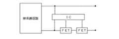
また、図11に示したように、被保護回路に直列にFETを設けると共に、FETによる電圧降下を検出するICを設け、FETによる電圧降下が一定値以上になった場合にICがFETを動作させてFETが被保護回路への電流を遮断するようにした保護装置が知られている。 In addition, as shown in FIG. 11, an FET is provided in series with the protected circuit, and an IC for detecting a voltage drop due to the FET is provided. When the voltage drop due to the FET exceeds a certain value, the IC operates the FET. A protection device is known in which the FET blocks the current to the protected circuit.
しかしながら、一般に、ヒューズは、定格電流以上の電流が流れた場合に直ちに溶断するというものではなく、定格電流よりも相当に大きな電流が或る程度の時間流れ続けた場合に初めて溶断する。例えば、UL規格においても、ヒューズ製品に関しては、「定格電流の2倍の電流が流れたときに、60秒以内に溶断すること」と定められている。そのため、定格3Aのヒューズを例にとると、3Aまでは溶断しないが、3Aより1mAでも多く流れた場合には直ちに自己発熱により溶断するというものは存在しない。 However, in general, a fuse does not blow immediately when a current exceeding the rated current flows, but only when a current considerably larger than the rated current continues to flow for a certain period of time. For example, also in the UL standard, for fuse products, it is defined that “when a current twice as large as the rated current flows, the fuse product is blown within 60 seconds”. Therefore, taking a fuse with a rating of 3A as an example, the fuse does not blow up to 3A, but there is no one that blows immediately due to self-heating when a flow of 1 mA more than 3A flows.
このように、定格電流と遮断電流(実際にヒューズが溶断するときの電流)との差が大きく、定格電流を超えても電流が直ちに遮断されることはないというヒューズの特性は、用途によっては、非常な不便さをもたらしている。 In this way, the difference between the rated current and the breaking current (current when the fuse actually blows) is large, and the fuse characteristics that the current is not immediately cut off even if the rated current is exceeded, Has brought about inconvenience.
このような不便さは、PTC素子にもある。即ち、PTC素子は、定格電流(トリップしない電流値)よりも最低でも2倍以上通電しないとトリップしない。 Such inconvenience is also present in the PTC element. That is, the PTC element does not trip unless it is energized at least twice as much as the rated current (current value that does not trip).
これに対して、図11に示したようにICとFETを組み合わせた保護装置では、ヒューズやPTC素子に比して定格電流と遮断電流の差を小さくすることができる。しかしながら、FETは、半導体であるため、電圧や電磁波が印加されることにより故障する場合があり、そのような故障が電流遮断時に発生した場合には、安全上格別問題はないが、通電時に発生した場合には、非常に危険である。 On the other hand, as shown in FIG. 11, in the protection device combining the IC and the FET, the difference between the rated current and the cutoff current can be reduced as compared with the fuse and the PTC element. However, since FET is a semiconductor, it may break down when voltage or electromagnetic waves are applied. If such a failure occurs when the current is interrupted, there is no particular safety problem, but it occurs when the current is applied. If you do, it is very dangerous.
また安全上、保護装置は、過電流が流れた場合だけでなく、周囲の光学的、磁気的、力学的な環境や、温度、湿度等の外部環境が何らかの理由で異常に変化した場合にも作動することが好ましい。 For safety reasons, the protective device is used not only when an overcurrent flows, but also when the surrounding optical, magnetic, or dynamic environment or the external environment such as temperature or humidity changes abnormally for some reason. It is preferable to operate.
本発明は以上のような従来技術の問題点を解決しようとするものであり、安全性が高く、かつ、所定の電流値を超える電流が流れた場合、あるいは外部の動作環境について何らかの異常が検知された場合には、速やかに電流を遮断又は抑制することのできる過電流保護装置を提供することを目的とする。 The present invention is intended to solve the problems of the prior art as described above, and is highly safe and detects an abnormality when a current exceeding a predetermined current value flows or an external operating environment is detected. In such a case, an object of the present invention is to provide an overcurrent protection device that can quickly cut off or suppress current.
本発明者らは、上記の目的を達成するためには、過電流時に低融点金属体又はPTC素子が自己発熱ではなく発熱体により加熱されるようにし、かつこの発熱体が、被保護回路への通電ラインにおける電圧降下量が所定の値を超えた場合、あるいは外部の動作環境異常を検出する外部センサが何らかの異常を検知した場合に、速やかに発熱するようにすること、そのために低融点金属体又はPTC素子の電圧降下量を検出する第1の検知素子と外部の動作環境異常を検出する外部センサとを設け、第1の検知素子が所定の電圧降下量を検出した場合、あるいは外部センサによって何らかの異常が検知された場合には、発熱体に急激に大電流を通電させるスイッチング素子を設けることが有効であることを見出し、本発明を完成させるに至った。 In order to achieve the above-mentioned object, the present inventors have made the low melting point metal body or the PTC element be heated by a heating element instead of self-heating at the time of overcurrent, and this heating element is transferred to the protected circuit. If the amount of voltage drop in the current line exceeds a predetermined value, or if an external sensor that detects an external operating environment abnormality detects any abnormality, heat is generated quickly. A first sensing element for detecting a voltage drop amount of the body or the PTC element and an external sensor for detecting an external operating environment abnormality, and the first sensing element detects a predetermined voltage drop amount, or an external sensor When any abnormality is detected by the above, it has been found that it is effective to provide a switching element that causes a large amount of current to rapidly flow through the heating element, and the present invention has been completed.
即ち、本発明は、基板上に、発熱体、及び低融点金属体又はPTC素子を有し、前記発熱体の発熱により低融点金属体の溶断又はPTC素子のトリップが生じる過電流保護装置において、被保護回路への通電ラインにおける電圧降下を検出する第1の検知素子、外部の動作環境異常を検出する外部センサ、及び前記第1の検知素子の電圧降下量又は前記外部センサからの信号に応じて発熱体に大電流を通し発熱体を急熱するスイッチング素子が設けられていることを特徴とする過電流保護装置を提供する。 That is, the present invention provides an overcurrent protection device having a heating element and a low melting point metal body or a PTC element on a substrate, wherein the heat generation of the heating element causes melting of the low melting point metal body or tripping of the PTC element. A first sensing element for detecting a voltage drop in the energization line to the protected circuit, an external sensor for detecting an external operating environment abnormality, and a voltage drop amount of the first sensing element or a signal from the external sensor An overcurrent protection device is provided in which a switching element for passing a large current through the heating element and rapidly heating the heating element is provided.
特に、このような過電流保護装置において、前記第1の検知素子としてICが設けられ、前記スイッチング素子としてFETが設けられているものを提供する。 In particular, such an overcurrent protection device is provided in which an IC is provided as the first detection element and an FET is provided as the switching element.
本発明によれば、安全性が高く、かつ、所定の電流値を超える電流が流れた場合、あるいは外部の動作環境について何らかの異常が検知された場合には、速やかに電流を遮断又は抑制することのできる過電流保護装置を得ることができる。 According to the present invention, when a current that is highly safe and exceeds a predetermined current value flows, or when any abnormality is detected in the external operating environment, the current is quickly cut off or suppressed. An overcurrent protection device capable of performing the above can be obtained.
以下、図面を参照しつつ本発明の過電流保護装置を詳細に説明する。なお、各図中、同一符号は同一又は同等の構成要素を表している。 Hereinafter, an overcurrent protection device of the present invention will be described in detail with reference to the drawings. In each figure, the same numerals indicate the same or equivalent components.
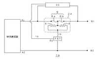
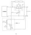
図1は、参考例の過電流保護装置1Aの回路図である。この過電流保護装置1Aは、基板上に発熱体4及び低融点金属体6を有してなる保護素子2Aを、被保護回路への通電ライン上に有している。また、この保護素子2Aの電圧降下を検出する第1の検知素子としてICを有し、ICにより検出された保護素子2Aの電圧降下量に応じて発熱体4に大電流を通すスイッチング素子として、FETを有している。即ち、このFETは、ICにより検出された保護素子2Aの電圧降下量に応じてゲート電位EGが変化し、そのゲート電位EGの変化に応じて発熱体4に急激に大電流を通す。 FIG. 1 is a circuit diagram of an overcurrent protection device 1A of a reference example. This overcurrent protection device 1A has a protection element 2A having a
図10は、保護素子2Aの平面図(同図(a))及び断面図(同図(b))である。この保護素子2A自体は、発熱体4の発熱により低融点金属体6が溶断する公知のものであり(特許第2790433号、特開平8−161990号公報)、基板3上に発熱体4、絶縁層5、低融点金属体6が順次積層された構造を有する。 10A and 10B are a plan view (FIG. 10A) and a cross-sectional view (FIG. 10B) of the protection element 2A. The protective element 2A itself is a known element in which the low melting
ここで、基板3としては、特に制限はなく、プラスチックフィルム、ガラスエポキシ基板、セラミック基板、金属基板等を使用することができるが、無機系基板が好ましい。 Here, there is no restriction | limiting in particular as the board |
発熱体4は、例えば、酸化ルテニウム、カーボンブラック等の導電材料と水ガラス等の無機系バインダあるいは熱硬化性樹脂等の有機系バインダからなる抵抗ペーストを塗布し、必要に応じて焼成することにより形成される。また、発熱体4としては、酸化ルテニウム、カーボンブラック等の薄膜を印刷、メッキ、蒸着、スパッタで形成してもよく、これらのフィルムの貼付、積層等により形成したものでもよい。 The
低融点金属体6の形成材料としては、従来よりヒューズ材料として使用されている種々の低融点金属体を使用することができ、例えば、特開平8−161990号公報の段落[0019]の表1に記載の合金を使用することができる。 As a material for forming the low melting
また、図10の保護素子2Aにおいて、7a、7bは低融点金属体6用電極であり、7x、7yは発熱体4用電極であり、このうちの一方の電極7yによって2つの発熱体4が接続されている。8は、固形フラックス等からなる内側封止部で、低融点金属体6の表面酸化を防止している。9は、低融点金属体6よりも高融点又は高軟化点を有する材料からなる外側封止部で、低融点金属体6の溶断時に溶融物がこの保護素子2Aの外へ流出することを防止している。 Further, in the protective element 2A of FIG. 10, 7a and 7b are electrodes for the low melting
図1の過電流保護装置1Aの回路図において、端子A1、A2には、例えばリチウムイオン電池、モーター等の被保護回路の電極端子が接続され、端子B1、B2には、被保護回路に接続して使用される充電器等の装置の電極端子が接続される。この過電流保護装置1Aによれば、過電流時に保護素子2Aの電圧降下が所定の値より大きくなると、ICが動作してFETのゲート電位EGを変化させ、これによりFETが動作して急激にゲート電流iG が流れ、大きなドレイン電流iD が発熱体4に急激に流れ、発熱体4が急熱される。この熱は、発熱体4上の低融点金属体6に速かに伝達し、低融点金属体6が溶断し、被保護回路への過電流が遮断される。なおこの場合、低融点金属体6は、6a、6bの2カ所で溶断するので、低融点金属体6の溶断の後は、発熱体4への通電は完全に遮断される。 In the circuit diagram of the overcurrent protection device 1A in FIG. 1, the terminals A1, A2 are connected to electrode terminals of a protected circuit such as a lithium ion battery or a motor, and the terminals B1, B2 are connected to the protected circuit. The electrode terminal of a device such as a charger is connected. According to this overcurrent protection device 1A, when the voltage drop of the protection element 2A becomes larger than a predetermined value at the time of overcurrent, the IC operates to change the gate potential EG of the FET. The gate current iG flows, the large drain current iD flows rapidly to the
このように、この過電流保護装置1Aによれば、保護素子2Aに所定の電流を超える過電流が流れた場合に、保護素子2Aの低融点金属体6を速やかに溶断させることができる。また、保護素子2Aの電圧降下を検出するIC及び発熱体4に通電させるFETとして、所定の動作電圧を有するものを適宜選択することにより、過電流時に低融点金属体6を溶断させる電流値(遮断電流値)を任意に設定することができる。 Thus, according to this overcurrent protection device 1A, when an overcurrent exceeding a predetermined current flows through the protection element 2A, the low melting
さらに、FETには、正常時には通電されないため、仮にFETが故障しても、その故障によって被保護回路の安全性が損なわれることはない。即ち、FETがON状態で故障した場合には、低融点金属体6が溶断して電流が遮断される。反対にOFF状態で故障した場合には、FETによって発熱体4に通電されることはないので、発熱体4の発熱によって低融点金属体6が溶断することはないが、過電流時には、低融点金属体6の自己発熱により低融点金属体6が溶断する。したがって、従来の電流ヒューズと同程度の安全性が確保される。 Furthermore, since the FET is not energized in the normal state, even if the FET fails, the safety of the protected circuit is not impaired by the failure. That is, when the FET fails in the ON state, the low melting
図2は、参考例の他の態様の過電流保護装置1Bの回路図である。この過電流保護装置1Bは、図1の過電流保護装置1Aの保護素子2Aに直列に抵抗体11を挿入すると共に、第1の検知素子であるICが、この抵抗体11の電圧降下を検出するようにしたものである。したがって、この過電流保護装置1Bによれば、抵抗体11の電圧降下が所定の値より大きくなった場合にICが動作し、これによりFETが動作して急激に発熱体4に電流が流れ、発熱体4が急熱される。 FIG. 2 is a circuit diagram of an overcurrent protection device 1B according to another aspect of the reference example. In this overcurrent protection device 1B, a resistor 11 is inserted in series with the protection element 2A of the overcurrent protection device 1A in FIG. 1, and an IC which is a first detection element detects a voltage drop of the resistor 11. It is what you do. Therefore, according to this overcurrent protection device 1B, when the voltage drop of the resistor 11 becomes larger than a predetermined value, the IC operates, whereby the FET operates and a current flows rapidly to the
図3は、参考例の他の態様の過電流保護装置1Cの回路図である。この過電流保護装置1Cは、図1の過電流保護装置1Aの保護素子2Aに代えて、PTC素子10と低融点金属体6の双方が発熱体4に近接して設けられている保護素子2Bを使用したものである。このように、PTC素子10と低融点金属体6とを発熱体4上で直列に接続した保護素子2B自体としては公知のもの(特開平8−236305号公報)を使用することができる。 FIG. 3 is a circuit diagram of an
かかる保護素子2Bを使用することにより、過電流時の発熱体4の発熱で、まず、PTC素子10を作用させて電流を抑制し、このPTC素子10の電流抑制作用後に電流が正常に戻った場合には、引き続きこの過電流保護装置1Cを使用することが可能となる。一方、PTC素子10の電流抑制作用後にもなお過電流が流れる場合には、低融点金属体6が溶断する。したがって、この保護素子2Bを使用することにより、過電流時にまずPTC素子10を作用させて回路の再使用を可能な限り確保し、かつ、低融点金属体6の作用により過電流から被保護回路を確実に保護することができる。 By using the protective element 2B, the heat generation of the
図4の過電流保護装置1Dは、図3の過電流保護装置1Cの変形例である。この過電流保護装置1Dでは、上述の保護素子2Bに代えて、PTC素子10と低融点金属体6の双方を発熱体4に近接させて設けたもの2組を備えた保護素子2Cを使用している。図3の過電流保護装置1Cでは、低融点金属体6が溶断した後にも発熱体4への通電が持続されることが考えられるが、図4の過電流保護装置1Dでは、低融点金属体6が溶断した後は、発熱体4への通電を確実に遮断することができ、回路の安全性を高めることができる。 An overcurrent protection device 1D in FIG. 4 is a modification of the
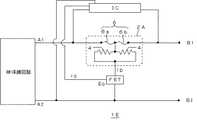
図5は、さらに異なる参考例の過電流保護装置1Eの回路図である。この過電流保護装置1Eは、図1の過電流保護装置1Aに対して、ICが、保護素子2Aの電圧降下を検出してFETを動作させるという第1の検知素子の機能だけでなく、被保護回路の端子電圧を検出し、その端子電圧に応じてFETを動作させるという第2の検知素子の機能も備えたものである。この過電流保護装置1Eによれば、被保護回路への過電流を防止するだけでなく、被保護回路の端子A1、A2間に所定電圧を超える過電圧が発生した場合にも、直ちにFETを動作させ、発熱体4に大電流を通して発熱体4を急熱し、速やかに低融点金属体6を溶断することができる。したがって、例えば、端子A1、A2にリチウムイオン電池等の電極端子を接続し、端子B1、B2に充電器等の電極端子を接続することにより、リチウムイオン電池の過充電を防止することができる。 FIG. 5 is a circuit diagram of an overcurrent protection device 1E of still another reference example. This overcurrent protection device 1E is different from the overcurrent protection device 1A of FIG. 1 in that the IC detects not only the voltage drop of the protection device 2A but also operates the FET, as well as the function of the first detection device. It also has a second sensing element function of detecting the terminal voltage of the protection circuit and operating the FET according to the terminal voltage. This overcurrent protection device 1E not only prevents overcurrent to the protected circuit, but also immediately operates the FET when an overvoltage exceeding a predetermined voltage occurs between the terminals A1 and A2 of the protected circuit. Then, the
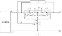
図6は、図5の過電流保護装置1Eにおいて、FETと接続するICの端子に外部センサを接続した本発明の過電流保護装置1Fの回路図である。この過電流保護装置1Fによれば、保護素子2Aの電圧降下量に応じて、あるいは被保護回路の端子(A1,A2)電圧に応じてFETのゲート電位EGが変化するだけでなく、外部センサからの信号に応じてもFETのゲート電位EGが変化し、発熱体4に大電流が流れ、低融点金属体6が溶断し、被保護回路への電流を遮断することが可能となる。 FIG. 6 is a circuit diagram of the overcurrent protection device 1F of the present invention in which an external sensor is connected to the terminal of the IC connected to the FET in the overcurrent protection device 1E of FIG. According to this overcurrent protection device 1F, not only does the gate potential EG of the FET change according to the voltage drop amount of the protection element 2A or the terminal (A1, A2) voltage of the protected circuit, but also an external sensor The gate potential EG of the FET also changes in response to the signal from, so that a large current flows through the
ここで、外部センサとしては、外部の動作環境異常に応じて信号を発するものを種々使用することができ、光センサ、磁気センサ、温度センサ、湿度センサ、圧力センサ、速度センサ、位置センサ、流量センサ、ガスセンサ、イオンセンサ等をあげることができる。より具体的には、例えば、光導電素子、フォトダイオード、フォトトランジスタ、フォトカプラ、LCD、焦電型赤外線センサ、熱電対、サーミスタ、ポジスタホール素子、磁気抵抗素子、感圧ダイオード、圧電素子、湿度センサ(無機塩、セラミックス又は高分子材料を使用したもの)、ジャイロ、光ファイバ等をあげることができる。これらは、トランジスタやマイコン等と電子回路を構成し、外部の動作環境異常に応じてFETのゲート電位EGを変化させる機能を有するものとなる。 Here, various types of external sensors that emit signals in response to abnormal operating environments can be used. Optical sensors, magnetic sensors, temperature sensors, humidity sensors, pressure sensors, speed sensors, position sensors, flow rates A sensor, a gas sensor, an ion sensor, etc. can be mentioned. More specifically, for example, photoconductive element, photodiode, phototransistor, photocoupler, LCD, pyroelectric infrared sensor, thermocouple, thermistor, posistor Hall element, magnetoresistive element, pressure sensitive diode, piezoelectric element, humidity Examples include sensors (using inorganic salts, ceramics, or polymer materials), gyros, optical fibers, and the like. These constitute an electronic circuit with a transistor, a microcomputer, etc., and have a function of changing the gate potential EG of the FET in response to an abnormal operating environment.
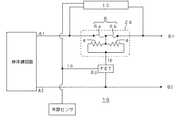
このような外部センサは、前述の図1〜図4の参考例の過電流保護装置1A、1B、1C、1Dにも設けることができる。例えば、図7は、図1の過電流保護装置1AのICに外部センサを接続した本発明の過電流保護装置1Gの回路図である。これにより、保護素子2Aの電圧降下量に応じて、あるいは外部センサからの信号に応じて、FETのゲート電位EGを変化させ、発熱体4に大電流を流し、低融点金属体6を溶断して被保護回路への電流を遮断することができる。 Such an external sensor can also be provided in the
図8は、さらに異なる本発明の過電流保護装置1Hの回路である。この過電流保護装置1Hは、図7の過電流保護装置1Gにおいて、保護素子2Aの電圧降下を検出するという第1の検出素子としての機能をICから省略したものとなっている。このように、本発明の過電流保護装置は、外部センサを設けた場合には、被保護回路への通電ラインにおける電圧降下を検出する第1の検知素子は省略したものも包含する。 FIG. 8 shows a further different circuit of the overcurrent protection device 1H of the present invention. This overcurrent protection device 1H is the same as the overcurrent protection device 1G of FIG. 7 except that the function as the first detection element for detecting the voltage drop of the protection element 2A is omitted from the IC. As described above, the overcurrent protection device of the present invention includes one in which the first detection element for detecting the voltage drop in the energization line to the protected circuit is omitted when an external sensor is provided.
この他、本発明は種々の態様をとることができる。例えば、スイッチング素子として、FETに代えて通常のバイポーラ型のトランジスタ、リレー等を用いてもよい。装置の小型化の点からは、FETが好ましい。 In addition, the present invention can take various forms. For example, a normal bipolar transistor, a relay, or the like may be used as the switching element instead of the FET. From the viewpoint of miniaturization of the device, FET is preferable.
また、本発明において、基板上に発熱体及び低融点金属体を有する保護素子としては、低融点金属体が発熱体の発熱で速やかに溶断するように、低融点金属体が発熱体と十分に近接して設けられていればよい。したがって、図10に示した保護素子2Aのように、低融点金属体6が発熱体4上に絶縁層5を介して積層している態様の他、特開平10−116549号公報、特開平10−116550号公報に記載されているように、発熱体と低融点金属体が基板上に平面的に配置されている態様としてもよく、特願平11−94385号明細書に記載されているように、低融点金属体が発熱体上に絶縁層を介することなく積層されている態様としてもよい。 In the present invention, the protective element having a heating element and a low-melting-point metal body on the substrate is sufficiently low-melting-point metal body and the heating element so that the low-melting-point metal body is quickly melted by the heat generated by the heating element. What is necessary is just to be provided close. Accordingly, as in the protective element 2A shown in FIG. 10, the low melting
基板上に発熱体及びPTC素子を有する保護素子についても同様に、PTC素子が発熱体の発熱で速やかにトリップするように、PTC素子が発熱体に十分近接して設けられていればよい。したがって、PTC素子が、発熱体上に絶縁層を介して積層されていてもよく、発熱体と平面的に配置されていてもよく、さらには、絶縁層を介することなく発熱体上に積層されていてもよい。 Similarly, for the protective element having the heating element and the PTC element on the substrate, the PTC element only needs to be provided sufficiently close to the heating element so that the PTC element trips quickly due to the heat generated by the heating element. Therefore, the PTC element may be laminated on the heating element via an insulating layer, may be arranged in a plane with the heating element, and further laminated on the heating element without an insulating layer. It may be.
さらに第1の検知素子、スイッチング素子及び第2の検知素子は、それぞれ別個のチップとして構成してもよいが、それらの機能を合わせ備えた1個のチップとして構成してもよい。 Furthermore, the first detection element, the switching element, and the second detection element may be configured as separate chips, but may be configured as a single chip having these functions.
以下、本発明を実施例に基づいて具体的に説明する。 Hereinafter, the present invention will be specifically described based on examples.
参考例1及び比較例1、2
図1の過電流保護装置1Aを構成した。この場合、保護素子2Aとしては、アルミナ系セラミック基板3上に、発熱体4として酸化ルテニウムペーストを印刷し(厚さ10μm)、水ガラス等の無機系バインダからなる絶縁層(厚さ10μm)5を介して、低融点金属体6としてSn:Pb=5:95(大きさ:1mm×6mm×100μm)を設けたものを使用した(図10参照)。保護素子2Aの電圧降下を検出するICとしては、セイコー電子工業社製S−80745SLを使用し、発熱体4に急激に大電流を通すFETとしては、三洋電機社製CPH3403を用いた。Reference Example 1 and Comparative Examples 1 and 2
The overcurrent protection device 1A of FIG. 1 was configured. In this case, as the protective element 2A, a ruthenium oxide paste is printed as the
得られた過電流保護装置1Aに対して、(a)定格電流、(b)最低保証遮断電流値、(c)最低保証遮断電流値での動作時間、を次のようにして求めた。また、比較例1、2として、市販の電流ヒューズ(定格電流2A)、市販のPTC素子(定格電流2A)についても同様に、(a)定格電流、(b)最低保証遮断電流値、(c)最低保証遮断電流値での動作時間を求めた。結果を表1に示す。 For the obtained overcurrent protection device 1A, (a) rated current, (b) minimum guaranteed cutoff current value, and (c) operating time at the minimum guaranteed cutoff current value were determined as follows. In addition, as Comparative Examples 1 and 2, for a commercially available current fuse (rated current 2A) and a commercially available PTC element (rated current 2A), (a) rated current, (b) minimum guaranteed breaking current value, (c ) The operating time at the minimum guaranteed cut-off current value was obtained. The results are shown in Table 1.
(a)定格電流:溶断あるいはトリップしないで通電することができる最大電流値
(b)最低保証遮断電流値:120秒以内の通電で、必ず溶断あるいはトリップする最小電流値
(c)最低保証遮断電流値での動作時間:最低保証遮断電流値で通電した場合に、溶断あるいはトリップが生じるまでの時間(a) Rated current: Maximum current value that can be energized without fusing or tripping
(b) Minimum guaranteed cut-off current value: The minimum current value that will always blow or trip when energized within 120 seconds.
(c) Operating time at minimum guaranteed cut-off current value: Time until fusing or trip occurs when energized at the minimum guaranteed cut-off current value

表1の結果から、参考例1によれば、定格電流と遮断電流の差を小さくし、定格電流を超えてから電流が遮断されるまでの時間を著しく短縮できることがわかる。 From the results of Table 1, it can be seen that according to Reference Example 1, the difference between the rated current and the breaking current can be reduced, and the time from when the rated current is exceeded until the current is cut off can be significantly shortened.
実施例1
図7の過電流保護装置1Gにおいて、雰囲気温度を検出する外部センサとして、図9に示すようにNTCサーミスタを用いた過電流保護装置1Iを構成した。この場合、保護素子2A、保護素子2Aの電圧降下を検出するIC1及びFETとしては、ぞれぞれ参考例1の過電流保護装置1Aで使用したものと同様とした。外部センサのNTCサーミスタとしては、BOWTHORPE THERMOMETRICS社製のDKF103B10(25℃において、10kΩ±10%)を使用した。外部センサのIC2としては、セイコー電子工業社製S−80737AL(検出電圧3.7V)を使用し、抵抗器R1、R2としては、それぞれカーボン皮膜抵抗器10kΩ、1kΩを使用した。Example 1
In the overcurrent protection device 1G of FIG. 7, an overcurrent protection device 1I using an NTC thermistor is configured as an external sensor for detecting the ambient temperature as shown in FIG. In this case, the protection element 2A, IC1 and FET for detecting the voltage drop of the protection element 2A were the same as those used in the overcurrent protection device 1A of Reference Example 1, respectively. As an NTC thermistor for the external sensor, DKF103B10 (10 kΩ ± 10% at 25 ° C.) manufactured by BOWTHORPE THERMOMETRICS was used. As IC2 of the external sensor, S-80737AL (detection voltage 3.7V) manufactured by Seiko Denshi Kogyo Co., Ltd. was used, and
この外部センサでは、雰囲気温度の上昇と共に、NTCサーミスタの抵抗が低下し、この抵抗の低下に比例してNTCサーミスタにかかる電圧が低下する。したがって、雰囲気温度の上昇と共に10kΩの抵抗器R1にかかる電圧が上昇する。また、IC2が10kΩの抵抗器R1の電圧降下を検出し、その検出電圧がある一定以上となった場合に、FETに信号を出力する。従ってこの外部センサを有する過電流保護装置1Iによると、雰囲気温度が一定以上に上昇し、10kΩの抵抗器R1の電圧降下量が一定以上になった場合に、外部センサのIC2から信号電圧がFETに出力され、FETのゲート電位EGが変化し、発熱体4に大電流が流れ、低融点金属体6が溶断し、被保護回路への電流を遮断する。 In this external sensor, as the ambient temperature increases, the resistance of the NTC thermistor decreases, and the voltage applied to the NTC thermistor decreases in proportion to the decrease in resistance. Therefore, the voltage applied to the 10 kΩ resistor R1 increases as the ambient temperature increases. IC2 detects a voltage drop of the resistor R1 of 10 kΩ, and outputs a signal to the FET when the detected voltage exceeds a certain level. Therefore, according to the overcurrent protection device 1I having this external sensor, when the ambient temperature rises above a certain level and the voltage drop across the 10kΩ resistor R1 exceeds a certain level, the signal voltage from the external sensor IC2 becomes FET. The gate potential EG of the FET changes, a large current flows through the
電源としてDC4Vを端子B1、B2間に接続し、雰囲気温度を25℃から110℃まで変化させたところ、雰囲気温度が100℃に到達したときに外部センサからFETに信号電圧が印加され、被保護回路への電流が遮断された。 When DC4V is connected as a power source between terminals B1 and B2 and the ambient temperature is changed from 25 ° C to 110 ° C, the signal voltage is applied from the external sensor to the FET when the ambient temperature reaches 100 ° C. The current to the circuit was interrupted.
本発明によれば、安全性が高く、かつ、所定の電流値を超える電流が流れた場合、あるいは外部の動作環境について何らかの異常が検知された場合には、速やかに電流を遮断又は抑制することのできる過電流保護装置を得ることができる。 According to the present invention, when a current that is highly safe and exceeds a predetermined current value flows, or when any abnormality is detected in the external operating environment, the current is quickly cut off or suppressed. An overcurrent protection device capable of performing the above can be obtained.
1A、1B、1C、1D、1E、1F、1G、1H、1I 過電流保護装置
2A、2B、2C 保護素子
3 基板
4 発熱体
5 絶縁層
6 低融点金属体
7a、7b 低融点金属体用電極
7x、7y 発熱体用電極
8 内側封止部
9 外側封止部
10 PTC素子
11 抵抗体
1A, 1B, 1C, 1D, 1E, 1F, 1G, 1H, 1I Overcurrent protection device 2A, 2B,
Claims (4)
Translated fromJapaneseThe second detection element for detecting the terminal voltage of the protected circuit is provided, and the switching element passes a large current through the heating element according to the terminal voltage, and rapidly heats the heating element. An overcurrent protection device according to claim 1.
Priority Applications (1)
| Application Number | Priority Date | Filing Date | Title |
|---|---|---|---|
| JP2005119779AJP2005243652A (en) | 1999-04-23 | 2005-04-18 | Overcurrent protective device |
Applications Claiming Priority (2)
| Application Number | Priority Date | Filing Date | Title |
|---|---|---|---|
| JP11701199 | 1999-04-23 | ||
| JP2005119779AJP2005243652A (en) | 1999-04-23 | 2005-04-18 | Overcurrent protective device |
Related Parent Applications (1)
| Application Number | Title | Priority Date | Filing Date |
|---|---|---|---|
| JP11356726ADivisionJP2001006518A (en) | 1999-04-23 | 1999-12-15 | Overcurrent protective device |
Publications (1)
| Publication Number | Publication Date |
|---|---|
| JP2005243652Atrue JP2005243652A (en) | 2005-09-08 |
Family
ID=35025102
Family Applications (1)
| Application Number | Title | Priority Date | Filing Date |
|---|---|---|---|
| JP2005119779APendingJP2005243652A (en) | 1999-04-23 | 2005-04-18 | Overcurrent protective device |
Country Status (1)
| Country | Link |
|---|---|
| JP (1) | JP2005243652A (en) |
Cited By (16)
| Publication number | Priority date | Publication date | Assignee | Title |
|---|---|---|---|---|
| JP2009070805A (en)* | 2007-08-20 | 2009-04-02 | Uchihashi Estec Co Ltd | Substrate type temperature fuse with resistor and secondary battery protection circuit |
| JP2009539420A (en)* | 2006-05-19 | 2009-11-19 | エシコン エンド−サージェリー,インク. | Electric surgical instrument |
| US7959050B2 (en) | 2005-07-26 | 2011-06-14 | Ethicon Endo-Surgery, Inc | Electrically self-powered surgical instrument with manual release |
| US8028885B2 (en) | 2006-05-19 | 2011-10-04 | Ethicon Endo-Surgery, Inc. | Electric surgical instrument with optimized power supply and drive |
| US8269121B2 (en) | 2006-05-19 | 2012-09-18 | Ethicon Endo-Surgery, Inc. | Force switch |
| US8627993B2 (en) | 2007-02-12 | 2014-01-14 | Ethicon Endo-Surgery, Inc. | Active braking electrical surgical instrument and method for braking such an instrument |
| US8627995B2 (en) | 2006-05-19 | 2014-01-14 | Ethicon Endo-Sugery, Inc. | Electrically self-powered surgical instrument with cryptographic identification of interchangeable part |
| WO2015156019A1 (en)* | 2014-04-07 | 2015-10-15 | デクセリアルズ株式会社 | Protection element, protection circuit and battery circuit |
| KR20160050025A (en) | 2013-09-06 | 2016-05-10 | 데쿠세리아루즈 가부시키가이샤 | Protection circuit |
| US9554803B2 (en) | 2005-07-26 | 2017-01-31 | Ethicon Endo-Surgery, Llc | Electrically self-powered surgical instrument with manual release |
| US9662116B2 (en) | 2006-05-19 | 2017-05-30 | Ethicon, Llc | Electrically self-powered surgical instrument with cryptographic identification of interchangeable part |
| US9848872B2 (en) | 2005-07-26 | 2017-12-26 | Ethicon Llc | Surgical stapling and cutting device |
| US10314583B2 (en) | 2005-07-26 | 2019-06-11 | Ethicon Llc | Electrically self-powered surgical instrument with manual release |
| JP2020527930A (en)* | 2018-03-16 | 2020-09-10 | エルジー・ケム・リミテッド | Integrated switching equipment, and battery monitoring and protection systems including integrated switching equipment |
| CN112793383A (en)* | 2020-12-31 | 2021-05-14 | 镇江海姆霍兹传热传动系统有限公司 | Electric vehicle and electric heating device thereof |
| WO2022153872A1 (en)* | 2021-01-12 | 2022-07-21 | 株式会社オートネットワーク技術研究所 | Power supply control device |
- 2005
- 2005-04-18JPJP2005119779Apatent/JP2005243652A/enactivePending
Cited By (58)
| Publication number | Priority date | Publication date | Assignee | Title |
|---|---|---|---|---|
| US8672951B2 (en) | 2005-07-26 | 2014-03-18 | Ethicon Endo-Surgery, Inc. | Electrically self-powered surgical instrument with manual release |
| US12059150B2 (en) | 2005-07-26 | 2024-08-13 | Cilag Gmbh International | Surgical stapling and cutting device |
| US7959050B2 (en) | 2005-07-26 | 2011-06-14 | Ethicon Endo-Surgery, Inc | Electrically self-powered surgical instrument with manual release |
| US11234695B2 (en) | 2005-07-26 | 2022-02-01 | Cilag Gmbh International | Surgical stapling and cutting device |
| US11172930B2 (en) | 2005-07-26 | 2021-11-16 | Cilag Gmbh International | Electrically self-powered surgical instrument with manual release |
| US10314583B2 (en) | 2005-07-26 | 2019-06-11 | Ethicon Llc | Electrically self-powered surgical instrument with manual release |
| US9855038B2 (en) | 2005-07-26 | 2018-01-02 | Ethicon Llc | Surgical stapling and cutting device |
| US9848872B2 (en) | 2005-07-26 | 2017-12-26 | Ethicon Llc | Surgical stapling and cutting device |
| US9554803B2 (en) | 2005-07-26 | 2017-01-31 | Ethicon Endo-Surgery, Llc | Electrically self-powered surgical instrument with manual release |
| US9662116B2 (en) | 2006-05-19 | 2017-05-30 | Ethicon, Llc | Electrically self-powered surgical instrument with cryptographic identification of interchangeable part |
| US8269121B2 (en) | 2006-05-19 | 2012-09-18 | Ethicon Endo-Surgery, Inc. | Force switch |
| US8573459B2 (en) | 2006-05-19 | 2013-11-05 | Ethicon Endo-Surgery, Inc | Optimal tissue compression electrical surgical instrument |
| US8592700B2 (en) | 2006-05-19 | 2013-11-26 | Ethicon Endo-Surgery, Inc. | Force switch |
| US12096933B2 (en) | 2006-05-19 | 2024-09-24 | Cllag GmbH International | Electrical surgical instrument with differential rate of closing motion speed |
| US8627995B2 (en) | 2006-05-19 | 2014-01-14 | Ethicon Endo-Sugery, Inc. | Electrically self-powered surgical instrument with cryptographic identification of interchangeable part |
| US8292157B2 (en) | 2006-05-19 | 2012-10-23 | Ethicon Endo-Surgery, Inc. | Electrical surgical instrument with optimized power supply and drive |
| US8827138B2 (en) | 2006-05-19 | 2014-09-09 | Ethicon Endo-Sugery, Inc. | Method for operating an electrical surgical instrument with optimal tissue compression |
| US8844791B2 (en) | 2006-05-19 | 2014-09-30 | Ethicon Endo-Surgery, Inc. | Electrical surgical instrument with optimal tissue compression |
| US8872046B2 (en) | 2006-05-19 | 2014-10-28 | Ethicon Endo-Surgery, Inc. | Force switch |
| JP2009539420A (en)* | 2006-05-19 | 2009-11-19 | エシコン エンド−サージェリー,インク. | Electric surgical instrument |
| US12009166B2 (en) | 2006-05-19 | 2024-06-11 | Cilag Gmbh International | Force switch |
| US11759203B2 (en) | 2006-05-19 | 2023-09-19 | Cilag Gmbh International | Electrical surgical instrument with minimum closure distance for staple firing control |
| US9439651B2 (en) | 2006-05-19 | 2016-09-13 | Ethicon Endo-Surgery, Llc | Methods for cryptographic identification of interchangeable parts for surgical instruments |
| JP2011120924A (en)* | 2006-05-19 | 2011-06-23 | Ethicon Endo-Surgery Inc | Electrical surgical instrument |
| US8286846B2 (en) | 2006-05-19 | 2012-10-16 | Ethicon Endo-Surgery, Inc. | Method for operating an electrical surgical instrument with optimal tissue compression |
| US11183349B2 (en) | 2006-05-19 | 2021-11-23 | Ethicon Endo-Surgery, Inc | Force switch |
| US9622744B2 (en) | 2006-05-19 | 2017-04-18 | Ethicon Endo-Surgery, Llc | Electrical surgical instrument with one-handed operation |
| US9666389B2 (en) | 2006-05-19 | 2017-05-30 | Ethicon Endo-Surgery, Inc. | Force switch |
| US11172931B2 (en) | 2006-05-19 | 2021-11-16 | Cilag Gmbh International | Electrically self-powered surgical instrument with cryptographic identification of interchangeable part |
| US9675348B2 (en) | 2006-05-19 | 2017-06-13 | Ethicon Llc | Electrical surgical instrument with knife return |
| US9681873B2 (en) | 2006-05-19 | 2017-06-20 | Ethicon Llc | Electrical surgical stapling instrument with tissue compressive force control |
| US9687234B2 (en) | 2006-05-19 | 2017-06-27 | Ethicon L.L.C. | Electrical surgical instrument with optimized power supply and drive |
| US9713473B2 (en) | 2006-05-19 | 2017-07-25 | Ethicon Endo-Surgery, Inc. | Active braking electrical surgical instrument and method for braking such an instrument |
| US9757127B2 (en) | 2006-05-19 | 2017-09-12 | Ethicon Llc | Electrical surgical instrument with optimal tissue compression |
| US8573462B2 (en) | 2006-05-19 | 2013-11-05 | Ethicon Endo-Surgery, Inc. | Electrical surgical instrument with optimized power supply and drive |
| US8038046B2 (en) | 2006-05-19 | 2011-10-18 | Ethicon Endo-Surgery, Inc. | Electrical surgical instrument with optimized power supply and drive |
| US9901340B2 (en) | 2006-05-19 | 2018-02-27 | Ethicon Endo-Surgery, Inc. | Active braking electrical surgical instrument and method for braking such an instrument |
| US9934920B2 (en) | 2006-05-19 | 2018-04-03 | Ethicon Endo-Surgery, Inc. | Force switch |
| US10217582B2 (en) | 2006-05-19 | 2019-02-26 | Ethicon Endo-Surgery, Inc. | Force switch |
| JP2011120923A (en)* | 2006-05-19 | 2011-06-23 | Ethicon Endo-Surgery Inc | Electrical surgical instrument |
| US10314592B2 (en) | 2006-05-19 | 2019-06-11 | Ethicon Llc | Electrically self-powered surgical instrument with cryptographic identification of interchangeable part |
| US8028885B2 (en) | 2006-05-19 | 2011-10-04 | Ethicon Endo-Surgery, Inc. | Electric surgical instrument with optimized power supply and drive |
| US10586669B2 (en) | 2006-05-19 | 2020-03-10 | Ethicon-Endo Surgery, Inc. | Force switch |
| US10675022B2 (en) | 2006-05-19 | 2020-06-09 | Ethicon Llc | Electrical surgical instrument with optimal tissue compression |
| US8627993B2 (en) | 2007-02-12 | 2014-01-14 | Ethicon Endo-Surgery, Inc. | Active braking electrical surgical instrument and method for braking such an instrument |
| JP2009070805A (en)* | 2007-08-20 | 2009-04-02 | Uchihashi Estec Co Ltd | Substrate type temperature fuse with resistor and secondary battery protection circuit |
| KR20160050025A (en) | 2013-09-06 | 2016-05-10 | 데쿠세리아루즈 가부시키가이샤 | Protection circuit |
| CN106463305B (en)* | 2014-04-07 | 2019-03-08 | 迪睿合株式会社 | Protection element, protection circuit and battery circuit |
| CN106463305A (en)* | 2014-04-07 | 2017-02-22 | 迪睿合株式会社 | Protection element, protection circuit and battery circuit |
| KR102344667B1 (en)* | 2014-04-07 | 2021-12-30 | 데쿠세리아루즈 가부시키가이샤 | Protection element, protection circuit and battery circuit |
| KR20160142303A (en) | 2014-04-07 | 2016-12-12 | 데쿠세리아루즈 가부시키가이샤 | Protection element, protection circuit and battery circuit |
| JP2015201313A (en)* | 2014-04-07 | 2015-11-12 | デクセリアルズ株式会社 | Protection element, protection circuit and battery circuit |
| WO2015156019A1 (en)* | 2014-04-07 | 2015-10-15 | デクセリアルズ株式会社 | Protection element, protection circuit and battery circuit |
| US11682796B2 (en) | 2018-03-16 | 2023-06-20 | Lg Energy Solution, Ltd. | Integrated switching device, and battery monitoring and protecting system including integrated switching device |
| JP2020527930A (en)* | 2018-03-16 | 2020-09-10 | エルジー・ケム・リミテッド | Integrated switching equipment, and battery monitoring and protection systems including integrated switching equipment |
| US12100818B2 (en) | 2018-03-16 | 2024-09-24 | Lg Energy Solution, Ltd. | Integrated switching device, and battery monitoring and protecting system including integrated switching device |
| CN112793383A (en)* | 2020-12-31 | 2021-05-14 | 镇江海姆霍兹传热传动系统有限公司 | Electric vehicle and electric heating device thereof |
| WO2022153872A1 (en)* | 2021-01-12 | 2022-07-21 | 株式会社オートネットワーク技術研究所 | Power supply control device |
Similar Documents
| Publication | Publication Date | Title |
|---|---|---|
| KR100783339B1 (en) | Overcurrent protection device | |
| JP2005243652A (en) | Overcurrent protective device | |
| EP1748459B1 (en) | Electrical protection apparatus | |
| TWI398894B (en) | Protection element | |
| WO2005124964A1 (en) | Battery pack protecting circuit and battery pack | |
| JP3185962B2 (en) | Protection circuit and protection element | |
| KR101388354B1 (en) | The complex protection device of blocking the abnormal state of current and voltage | |
| KR20080041636A (en) | Electrical composite devices | |
| KR20160035588A (en) | Protection device | |
| TWI887295B (en) | Protection circuit, battery pack and operation method for protection circuit | |
| JP4046106B2 (en) | Battery pack protection circuit and battery pack | |
| TWI824067B (en) | Protection element and protection circuit | |
| JP7321731B2 (en) | Battery pack, protection circuit | |
| JP2001044003A (en) | Protective element | |
| JP2012129124A (en) | Circuit protective element and battery pack device using the same | |
| US11817694B2 (en) | Protection element and protection circuit for a battery | |
| JPH04264382A (en) | Heating element unit | |
| US11145442B2 (en) | Externally controlled thermal trip device, method and application for varistors | |
| JP2001325929A (en) | Protector for battery | |
| JP3985820B2 (en) | Temperature-sensitive circuit breaker membrane device and energizing circuit device using the same | |
| JP2000315451A (en) | Protection element | |
| JP2002100272A (en) | Thermo protector | |
| JP3985800B2 (en) | Temperature-sensitive circuit breaker film and current-carrying circuit using the same | |
| JP2001025158A (en) | Protective circuit, and composite element used therefor | |
| JP2001312950A (en) | Thermal fuse having self-heating element and pack battery with the built-in thermal fuse |
Legal Events
| Date | Code | Title | Description |
|---|---|---|---|
| A131 | Notification of reasons for refusal | Free format text:JAPANESE INTERMEDIATE CODE: A131 Effective date:20080205 | |
| A521 | Written amendment | Free format text:JAPANESE INTERMEDIATE CODE: A523 Effective date:20080404 | |
| A02 | Decision of refusal | Free format text:JAPANESE INTERMEDIATE CODE: A02 Effective date:20080513 |