JP2005242797A - Error correction circuit - Google Patents
Error correction circuitDownload PDFInfo
- Publication number
- JP2005242797A JP2005242797AJP2004053317AJP2004053317AJP2005242797AJP 2005242797 AJP2005242797 AJP 2005242797AJP 2004053317 AJP2004053317 AJP 2004053317AJP 2004053317 AJP2004053317 AJP 2004053317AJP 2005242797 AJP2005242797 AJP 2005242797A
- Authority
- JP
- Japan
- Prior art keywords
- data
- bit
- circuit
- error
- address
- Prior art date
- Legal status (The legal status is an assumption and is not a legal conclusion. Google has not performed a legal analysis and makes no representation as to the accuracy of the status listed.)
- Pending
Links
Images


Classifications
- G—PHYSICS
- G06—COMPUTING OR CALCULATING; COUNTING
- G06F—ELECTRIC DIGITAL DATA PROCESSING
- G06F11/00—Error detection; Error correction; Monitoring
- G06F11/07—Responding to the occurrence of a fault, e.g. fault tolerance
- G06F11/08—Error detection or correction by redundancy in data representation, e.g. by using checking codes
- G06F11/10—Adding special bits or symbols to the coded information, e.g. parity check, casting out 9's or 11's
- G06F11/1008—Adding special bits or symbols to the coded information, e.g. parity check, casting out 9's or 11's in individual solid state devices
- G06F11/1048—Adding special bits or symbols to the coded information, e.g. parity check, casting out 9's or 11's in individual solid state devices using arrangements adapted for a specific error detection or correction feature
- G—PHYSICS
- G11—INFORMATION STORAGE
- G11C—STATIC STORES
- G11C29/00—Checking stores for correct operation ; Subsequent repair; Testing stores during standby or offline operation
- G11C29/04—Detection or location of defective memory elements, e.g. cell constructio details, timing of test signals
- G11C2029/0411—Online error correction
Landscapes
- Engineering & Computer Science (AREA)
- Theoretical Computer Science (AREA)
- Quality & Reliability (AREA)
- Physics & Mathematics (AREA)
- General Engineering & Computer Science (AREA)
- General Physics & Mathematics (AREA)
- Techniques For Improving Reliability Of Storages (AREA)
- For Increasing The Reliability Of Semiconductor Memories (AREA)
- Error Detection And Correction (AREA)
Abstract
Description
Translated fromJapaneseこの発明は、主としてフラッシュメモリを内蔵するマイクロコンピュータ等の集積回路において、フラッシュメモリのデータの信頼性向上を図る技術に関する。 The present invention relates to a technique for improving the reliability of data in a flash memory mainly in an integrated circuit such as a microcomputer incorporating a flash memory.
従来、フラッシュメモリを内蔵するマイクロコンピュータ(マイコンと略称する)等の集積回路は、フラッシュメモリに記憶したデータの信頼性向上を図るために、誤り検出・訂正(エラーチェッキング・アンド・コレクティング:ECCと略称する)回路を搭載していた。この理由は、フラッシュメモリはデータ・リテンションおよび書き込み・読み出し時の外乱などにより、記憶したデータが変化してしまう可能性があるためである。特に、マイコンの動作プログラムの記憶装置としてフラッシュメモリを使用する場合、1ビットでも誤ったデータをCPUが受け取ると、それにより誤動作するため、フラッシュメモリにはアドレス毎に本来のデータと共にデータ誤りチェック用のチェックビットが付加されて記憶される。例えば、32ビット幅のメモリデータに対して、6ビットのチェックビットが付加されることになる。 2. Description of the Related Art Conventionally, an integrated circuit such as a microcomputer (abbreviated as a microcomputer) incorporating a flash memory has been designed to detect and correct errors (error checking and correcting) in order to improve the reliability of data stored in the flash memory. (Abbreviated as ECC). This is because the stored data may change in the flash memory due to disturbances during data retention and writing / reading. In particular, when a flash memory is used as a storage device for microcomputer operation programs, if the CPU receives incorrect data even with one bit, it malfunctions accordingly, so the flash memory is used for data error checking along with the original data for each address. The check bit is added and stored. For example, 6 check bits are added to 32-bit memory data.
ECC回路は、そのメモリデータとチェックビットとを受け取って、1ビットのエラーの訂正、または、2ビット以上のエラー検出を行い、CPUにデータを転送している。
しかしながら、32ビット幅のメモリデータに対して6ビットのチェックビットを付加するような従来のECC回路では、フラッシュメモリの同一アドレスの1ビットエラーは訂正できるが、2ビット以上のエラーは訂正出来ないという問題があり、マイコンのプログラムの記憶装置としてフラッシュメモリを使用している場合、同一アドレスに2ビット以上のエラーが発生した時点で、マイコンが誤動作するという問題があった。 However, a conventional ECC circuit that adds 6 check bits to 32-bit memory data can correct a 1-bit error at the same address of a flash memory, but cannot correct an error of 2 bits or more. When a flash memory is used as a microcomputer program storage device, the microcomputer malfunctions when an error of 2 bits or more occurs at the same address.
本発明の課題は、前記問題点を解決して、2ビット以上のエラーに対処し得るエラー訂正回路を提供することにある。 An object of the present invention is to provide an error correction circuit capable of solving the above-mentioned problems and capable of dealing with an error of 2 bits or more.
この発明のエラー訂正回路は、前記課題を解決するために、第一の信号に基づいて記憶装置からのメモリデータとチェックデータから成る出力データの誤りビットの値を反転する選択ビット反転回路と、選択ビット反転回路の出力データに基づいてメモリデータの1ビットの誤りを訂正するECC回路と、ECC回路の出力する訂正データに基づいてチェックビットを生成するチェックビット生成回路と、訂正データとチェックビットを格納するECCデータレジスタと、選択ビット反転回路からの出力データAとECCデータレジスタの出力データA'とをビット比較するビット比較回路と、ビット比較回路がデータAとデータA’との不一致を検出した際に、当該メモリデータのアドレスを記憶するアドレス記憶部と、ビット比較回路がデータAとデータA’との不一致を検出した際に、当該不一致ビット位置にビット不一致を示す情報を書き込む誤りビット記憶回路を所定データ幅分備えた誤りデータ記憶部と、複数の誤りデータ記憶部に記憶された各データの論理OR演算を行って、第一の信号を生成するデータOR回路と、を備えている。 In order to solve the above problem, the error correction circuit of the present invention is a selection bit inversion circuit that inverts an error bit value of output data composed of memory data and check data from a storage device based on a first signal; An ECC circuit that corrects an error of one bit of memory data based on output data of the selected bit inversion circuit, a check bit generation circuit that generates a check bit based on correction data output from the ECC circuit, correction data, and a check bit ECC data register storing bit, bit comparison circuit for bit comparison between output data A from the selected bit inversion circuit and output data A ′ of the ECC data register, and the bit comparison circuit detects mismatch between data A and data A ′. When detected, the address storage unit for storing the address of the memory data, and the bit comparison circuit performs data A and data When an inconsistency is detected, an error data storage unit having an error bit storage circuit for writing a bit mismatch information at the mismatch bit position for a predetermined data width, and each of the error data storage units stored in the plurality of error data storage units A data OR circuit that performs a logical OR operation on the data to generate a first signal.
この発明によれば、従来の32ビット幅のデータに6ビットのチェックビットを用いるECC回路だけでは訂正出来ない2ビット以上のエラー訂正が可能となる。従って、フラッシュメモリに動作プログラムを格納したマイコン等の集積回路は、同一アドレスに2ビット以上のエラーが発生しても誤動作することが無く、信頼性の向上を図ることができる。また、エラーデータのアドレスを格納するアドレス記憶部と誤りデータ記憶部の数を自由に変更することが出来るため、フラッシュメモリの信頼性に応じた適切な回路規模を選択出来る。 According to the present invention, it is possible to perform error correction of 2 bits or more, which cannot be corrected only by an ECC circuit using 6-bit check bits for conventional 32-bit width data. Therefore, an integrated circuit such as a microcomputer that stores an operation program in a flash memory does not malfunction even if an error of 2 bits or more occurs in the same address, and can improve reliability. In addition, since the number of address storage units for storing error data addresses and the number of error data storage units can be freely changed, an appropriate circuit scale corresponding to the reliability of the flash memory can be selected.
以下、この発明の実施の形態について、図面を用いて詳細に説明する。尚、図中の各構成要素はこの発明が理解できる程度に概略的に示してあるにすぎない。 Hereinafter, embodiments of the present invention will be described in detail with reference to the drawings. It should be noted that the constituent elements in the drawings are merely schematically shown to the extent that the present invention can be understood.
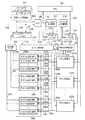
図1は、実施例1の構成を示すブロック図であり、この実施例のエラー訂正回路は、CPU100、フラッシュメモリ101、選択ビット反転回路105、1ビットのエラー訂正を行うECC回路108、フラッシュメモリデータレジスタ109、チェックビット生成回路111、ECCデータを保持するECCデータレジスタ113、CPU100から出力されるアドレスを記憶するアドレスレジスタ114、ECCデータレジスタ113からの出力データとフラッシュメモリデータレジスタ109からの出力データとをビット比較するビット比較回路115、フラッシュメモリデータレジスタ109等の各部のデータ設定タイミングを制御するタイミング制御回路118、誤りビットを記憶する誤りデータ記憶部128a〜128x、誤りの有ったアドレスを記憶するアドレス記憶部127a〜127x、前記誤りデータ記憶部128a〜128xおよびアドレス記憶部127a〜127xへのデータの書き込みを制御する書き込み制御回路125、および誤りデータ記憶部128a〜128xから出力される各データの論理OR演算を行うデータOR回路134により構成される。 FIG. 1 is a block diagram illustrating the configuration of the first embodiment. An error correction circuit according to the first embodiment includes a
図2は、書き込み制御回路125の回路図であり、図3は誤りデータ記憶部128a〜128x内の1ビットの誤り情報を記憶する誤りビット記憶回路の回路図であり、図4は、アドレス記憶部127a〜127xの内部の回路図である。 FIG. 2 is a circuit diagram of the
以下、図1〜図4の回路図および図5のタイムチャートを用いて動作を説明する。
読み出しサイクル(1)において、CPU100はt0のタイミングでアドレスデータ102を出力する。タイミング制御回路118からのアドレスラッチ信号121がt1のタイミングで”L"レベルから”H"レベルに変化し、その立ち上がりエッジでアドレスデータ102がアドレスレジスタ114に格納され、アドレスレジスタ114の出力データは図示のように1aとなる。The operation will be described below using the circuit diagrams of FIGS. 1 to 4 and the time chart of FIG.
In the read cycle (1), the
フラッシュメモリ101はアドレスデータ102を受けてt2のタイミングでメモリデータ103、チェックビットデータ104を出力する。メモリデータ103は、メモリの内容そのものであり、チェックビットデータ104はチェックビットを表すデータである。この時のメモリデータ103,チェックビットデータ104をデータAとし、メモリデータ103に1ビットの誤りがあるものとする。 The
この出力データは選択ビット反転回路105に入力され、信号135の内容に基づいてデータ103,104に対応するデータ106,107を出力する。このとき、初期状態では、誤りデータとそのアドレスが記憶されていないため、アドレス一致信号131(131a,131b,・・・131x)は全て”L”レベル(アドレス不一致:図4参照)となり、また、誤りデータ記憶部128a〜128xからの出力データ133(133a,133b,・・・、133x)も全て”L"レベルとなる(図3参照)。このため、ビットOR回路134の出力信号である反転ビット選択信号135(この信号はメモリデータ幅+チェックビット幅のデータ幅を有する信号である)は全て”L"レベルとなる。これにより、選択ビット反転回路105の出力データ106,107は反転されず、フラッシュメモリの出力データAと同一データとなる。This output data is input to the selected
ECC回路108は、選択ビット反転回路105の出力データ106,107を入力し、データの1ビットの誤りを訂正して訂正データ110を出力する。この訂正データ110は、読み出しサイクル(1)においてCPU100に取り込まれる。 The
タイミング制御回路118からのフラッシュメモリデータレジスタ109に対するデータラッチ信号119がt3のタイミングで”L"レベルから”H"レベルに変化し、その立ち上がりエッジで選択ビット反転回路105の出力データ106,107の内容がフラッシュメモリデータレジスタ109に取り込まれ、その出力データ116はデータAとなる。 The data latch signal 119 from the
チェックビット生成回路111は、ECC回路108による訂正データ110を受けて所定数ビット(例えば6ビット)から成るチェックビットデータ112を出力する。このチェックビットデータは、例えば、下記の多項式を用いて訂正データ110(例えば32ビット幅のデータ)から生成する。
タイミング制御回路118からのECCデータラッチ信号120がt4のタイミングで”L"レベルから”H"レベルに変化し、その立ち上がりエッジで訂正データ110、およびチェックビット出力データ112の内容A'がECCデータレジスタ113に取り込まれ、その出力データ117はA'となる。 The ECC data latch signal 120 from the
フラッシュメモリデータレジスタ109の出力データ116の内容AとECCデータレジスタ113の出力データ117の内容A'は、ビット比較回路115において比較され、A
とA'の差異の1ビット(データAの誤りビット)のみデータ”1”となり、その他のビットはデータ”0”として出力結果信号124が出力される。また、データAとA'に差異があることから、ビット比較回路115の誤り検出信号123が”L"レベルから”H"レベルに変化する。The content A of the
Only one bit (error bit of data A) of the difference between A and A ′ is data “1”, and the other bits are data “0”, and the
タイミング制御回路118からの書き込みタイミング制御信号122がt5のタイミングで”L"レベルから”H"レベルに変化し、それに伴い、書き込みイネーブル信号129aと書き込みビジー信号126が”L"レベルから”H"レベルに変化する。書き込みビジー信号126が”H"レベルに変化したのを受けて、タイミング制御回路118は、書き込みサイクルの開始と認識し、アドレスラッチ信号121、フラッシュメモリデータレジスタ109へのラッチ信号119,ECCデータレジスタ113へのデータラッチ信号120を”H"レベルから”L"レベルに変化させる。これらの信号は、書き込みサイクル中は”L"レベルに固定され、書き込みタイミング信号122は”H"レベルに固定される。 The write timing control signal 122 from the
一方アドレス記憶部127aの内部では、書き込みサイクル中は書き込みイネーブル信号129が”H"レベルとなり、アドレス記憶素子201の書き込みイネーブル信号(WE)が”H"レベルとなり、アドレスレジスタ114の内容がアドレス記憶素子201に書き込まれる。同時に、記憶素子205にデータ”1”が書き込まれる。 On the other hand, in the
誤りデータ記憶部128aにおいても書き込みサイクル中は書き込みイネーブル信号129aが”H"レベルになっているので、ビット比較回路115の出力データ124内のエラービットに対応する誤りビット記憶回路の記憶素子401の書き込みイネーブル信号(WE)が”H"レベルの時に記憶素子401にデータ”1”が書き込まれる。尚、各誤りデータ記憶部内部の誤りビット記憶回路は、データ幅とチェックビット幅に相当する数の回路(図1では32ビットのデータ幅と6ビットのチェックビットに対応して38回路)が設けられている。 Also in the error
アドレス記憶部127a及び誤りデータ記憶部128aへの書き込みが完了すると、タイミング制御部118は、書き込みタイミング制御信号122を”H"レベルから”L"レベルに変化させ、それに伴い、書き込みビジー信号126が”H"レベルから”L"レベルに変化し、書き込みサイクルが終了する。書き込みサイクル中に読み出しサイクルが有った場合は、フラッシュメモリデータレジスタ109、ECCデータレジスタ113、アドレスレジスタ114の各内容の更新が行われず、CPU100が必要な訂正データ110を取り込むのに影響は無い。 When the writing to the
読み出しサイクル(2)においては、アドレス2aのフラッシュメモリの出力メモリデータ103,104のデータBに1ビットの誤りが無いため、読み出しサイクル(1)と同じ動作でフラッシュメモリデータレジスタ109及びECCデータレジスタ113に保持されたデータは共にBとなる。このため、書き込みタイミング信号122が”H"レベルとなった時に誤り検出信号123は”L"レベルのままとなるために書き込みビジー信号126も”L"レベルのままとなり、書き込み動作は発生しない。 In the read cycle (2), there is no one-bit error in the data B of the
読み出しサイクル(3)において、再び1ビットの誤りのあるアドレス1aのフラッシュメモリメモリデータ103,104(データA)が出力された場合、アドレス記憶部127aのアドレス比較回路202においてアドレス出力102の内容1aと記憶素子201の内容が比較され、この場合両者が一致するのでアドレス一致信号131が”L"レベルから”H"レベルに変化する。アドレス一致信号131が”H"レベルになることにより、誤りデータ記憶部128aにおいて既にデータ”1”を書き込まれている誤りビット記憶回路の出力が”L"レベルから”H"レベルに変化する。その他の誤りビット記憶回路の出力は”L"レベルのままであるため、誤りデータ記憶部128a〜128xの出力信号133a〜133xの論理ORをとるデータOR回路134の出力である反転ビット選択信号135は、全て”L"レベルの状態から前記1ビット誤りに対応するビットのみが”H"レベルに変化する。 In the read cycle (3), when the flash
選択ビット反転回路105は、反転ビット選択信号135を受けて、フラッシュメモリの出力メモリデータ103,104のエラービットのみを反転させ、選択ビット反転回路105の出力データ106,107にデータA'を出力する。その後は、前記サイクル(1)と同じ動作でフラッシュメモリデータレジスタ109及びECCデータレジスタ113に保持されたデータは共にA'となる。このため、読み出しサイクル(2)と同じ動作により書き込み動作は発生しない。 The selection
その後の読み出しサイクルで別のアドレスのフラッシュメモリの出力メモリデータ103,104に1ビットのエラーが有った場合は、読み出しサイクル(1)と同様の動作により、今度は書き込みイネーブル信号129bが”L"レベルから”H"レベルに変化し、書き込みサイクル中に当該アドレスがアドレス記憶部127bに書き込まれ、ビット比較回路115のビット比較結果出力信号124に現れたエラービット位置は、誤りデータ記憶部128bの対応する誤りビット記憶回路に書き込まれる。 If there is a 1-bit error in the
尚、図1において、アドレス記憶部と誤りデータ記憶部は、フラッシュメモリの信頼性に応じて必要な数設けることが出来る。 In FIG. 1, a necessary number of address storage units and error data storage units can be provided according to the reliability of the flash memory.
アドレス1aのフラッシュメモリメモリデータ103,104において別の1ビットがエラーとなり、合計2ビットエラーとなった場合にも、選択ビット反転回路105の出力データ106,107の内容は、読み出しサイクル(1)の場合と同様に1ビットエラーとなるので(サイクル(1)でエラーとなったビットは選択ビット反転回路105により正しい値に反転されているので、新たにエラーとなった1ビットのみが出力される)、CPU100にはECC回路108で訂正された訂正データ110が供給される。その後は、読み出しサイクル(1)と同様に、ビット比較回路115におけるデータの差異により誤り検出信号123が”L"レベルから”H"レベルに変化するので、書き込み動作が発生する。但し、アドレス記憶部127aには既にアドレスが書き込まれているので、ビット比較回路115の出力データ124の内1ビット誤りに該当するビット記憶回路の記憶素子401(図3参照)書き込みイネーブル信号(WE)が”H"レベルに変化し、記憶素子401にデータ”1”が書き込まれる。 Even when another 1 bit becomes an error in the flash
このような動作を行うことにより、本発明によるエラー訂正回路においては、同一アドレスのフラッシュメモリの出力の全ビットがエラーとなってもCPU100には正しく訂正されたデータ110を提供することが出来る。 By performing such an operation, the error correction circuit according to the present invention can provide the
以上説明したように、実施例1によれば、従来の32ビット幅のデータに6ビットのチェックビットを用いるECC回路だけでは訂正出来ない2ビット以上のエラー訂正が可能となる。従って、フラッシュメモリに動作プログラムを格納したマイコン等の集積回路は、同一アドレスに2ビット以上のエラーが発生しても誤動作することが無く、信頼性の向上を図ることができる。また、書き込み制御回路125にわずかな変更を行うことにより、エラーデータのアドレスを格納するアドレス記憶部と誤りデータ記憶部の数を自由に変更することが出来るため、フラッシュメモリの信頼性に応じた適切な回路規模を選択出来る。 As described above, according to the first embodiment, it is possible to perform error correction of 2 bits or more that cannot be corrected only by the ECC circuit using 6-bit check bits for conventional 32-bit width data. Therefore, an integrated circuit such as a microcomputer that stores an operation program in a flash memory does not malfunction even if an error of 2 bits or more occurs in the same address, and can improve reliability. Further, by making a slight change to the
図6は、本発明による誤り訂正回路の実施例2の構成を示すブロック図であり、外部入力端子601と、この端子から入力される入力信号602がタイミング制御回路118に入力されている点が実施例1の構成と異なっている。
以下、図6を参照して実施例2の誤り訂正回路の動作を説明する。FIG. 6 is a block diagram showing the configuration of the error correction circuit according to the second embodiment of the present invention, in that an
The operation of the error correction circuit according to the second embodiment will be described below with reference to FIG.
外部入力端子601からの入力信号602が”L"レベルの場合、タイミング制御回路118において、アドレスラッチ信号121、フラッシュメモリデータラッチ信号119、ECCデータレジスタ113のラッチ信号120及び書き込みタイミング制御信号122は、”L"レベル(無効レベル)に固定されるように制御される。これにより、アドレスレジスタ114、フラッシュメモリデータレジスタ109、ECCデータレジスタ113はそれぞれデータを保持しなくなり、また、書き込みタイミング制御信号122が”L"レベルに固定されることにより、書き込み制御回路125の出力データの全てが”L"レベルに固定されるため、書き込み動作が停止する。 When the input signal 602 from the
一方、外部入力端子601からの入力信号602が”H"レベルの場合は、タイミング制御回路118において、アドレスラッチ信号121、フラッシュメモリデータラッチ信号119、ECCデータレジスタ113のラッチ信号120及び書き込みタイミング制御信号122は図5のタイムチャートに示されるように制御される。これにより、アドレスレジスタ114、フラッシュメモリデータレジスタ109、ECCデータレジスタ113はそれぞれのラッチ信号の立ち上がりエッジでデータを保持し、書き込みタイミング制御信号122が”H"レベルに変化することで書き込み制御回路125が動作し、書き込み動作が可能となる。 On the other hand, when the input signal 602 from the
以上説明したように、実施例2のエラー訂正回路によれば、外部入力端子601からの入力信号602に基づいて実施例1に示した機能を停止させることが可能となるため、フラッシュメモリの出荷試験時や、仮のデータをフラッシュメモリに格納して動作させる場合などにアドレス記憶部や誤りデータ記憶部に不要なデータが書き込まれるのを防止することが出来る。 As described above, according to the error correction circuit of the second embodiment, the function shown in the first embodiment can be stopped based on the input signal 602 from the
100 CPU
101 フラッシュメモリ
105 選択ビット反転回路
108 ECC回路
109 フラッシュメモリデータレジスタ
111 チェックビット生成回路
113 ECCデータレジスタ
114 アドレスレジスタ
115 ビット比較回路
118 タイミング制御回路
125 書き込み制御回路
127 アドレス記憶部
128 誤りデータ記憶部
134 データOR回路100 CPU
101
Claims (3)
Translated fromJapanese前記選択ビット反転回路の出力データに基づいて前記メモリデータの1ビットの誤りを訂正するECC回路と、
前記ECC回路の出力する訂正データに基づいてチェックビットを生成するチェックビット生成回路と、
前記訂正データと前記チェックビットを格納するECCデータレジスタと、
前記選択ビット反転回路からの出力データAと前記ECCデータレジスタの出力データA'とをビット比較するビット比較回路と、
前記ビット比較回路が前記データAとデータA’との不一致を検出した際に、当該メモリデータのアドレスを記憶するアドレス記憶部と、
前記ビット比較回路が前記データAとデータA’との不一致を検出した際に、当該不一致ビット位置にビット不一致を示す情報を書き込む誤りビット記憶回路を所定データ幅分備えた誤りデータ記憶部と、
前記複数の誤りデータ記憶部に記憶された各データの論理OR演算を行って、前記第一の信号を生成するデータOR回路と、
を備えていることを特徴とするエラー訂正回路。A selection bit inversion circuit that inverts an error bit value of output data composed of memory data and check data from the storage device based on the first signal;
An ECC circuit for correcting an error of one bit of the memory data based on output data of the selected bit inversion circuit;
A check bit generation circuit that generates a check bit based on the correction data output from the ECC circuit;
ECC data register for storing the correction data and the check bit;
A bit comparison circuit that performs bit comparison between the output data A from the selected bit inverting circuit and the output data A ′ of the ECC data register;
An address storage unit that stores an address of the memory data when the bit comparison circuit detects a mismatch between the data A and the data A ′;
An error data storage unit provided with an error bit storage circuit for writing a bit mismatch information at the mismatch bit position when the bit comparison circuit detects a mismatch between the data A and the data A ′;
A data OR circuit that performs a logical OR operation of each data stored in the plurality of error data storage units to generate the first signal;
An error correction circuit comprising:
Priority Applications (2)
| Application Number | Priority Date | Filing Date | Title |
|---|---|---|---|
| JP2004053317AJP2005242797A (en) | 2004-02-27 | 2004-02-27 | Error correction circuit |
| US11/057,150US7299400B2 (en) | 2004-02-27 | 2005-02-15 | Error correction circuit |
Applications Claiming Priority (1)
| Application Number | Priority Date | Filing Date | Title |
|---|---|---|---|
| JP2004053317AJP2005242797A (en) | 2004-02-27 | 2004-02-27 | Error correction circuit |
Publications (1)
| Publication Number | Publication Date |
|---|---|
| JP2005242797Atrue JP2005242797A (en) | 2005-09-08 |
Family
ID=34917899
Family Applications (1)
| Application Number | Title | Priority Date | Filing Date |
|---|---|---|---|
| JP2004053317APendingJP2005242797A (en) | 2004-02-27 | 2004-02-27 | Error correction circuit |
Country Status (2)
| Country | Link |
|---|---|
| US (1) | US7299400B2 (en) |
| JP (1) | JP2005242797A (en) |
Cited By (4)
| Publication number | Priority date | Publication date | Assignee | Title |
|---|---|---|---|---|
| US8069389B2 (en) | 2006-08-25 | 2011-11-29 | Samsung Electronics Co., Ltd. | Error correction circuit and method, and semiconductor memory device including the circuit |
| US8091010B2 (en) | 2006-12-29 | 2012-01-03 | Samsung Electronics Co., Ltd. | Error correction circuit and method for reducing miscorrection probability and semiconductor memory device including the circuit |
| US8812933B2 (en) | 2011-11-04 | 2014-08-19 | Samsung Electronics Co., Ltd. | Memory system and operating method thereof |
| US8885409B2 (en) | 2011-11-24 | 2014-11-11 | Samsung Electronics Co., Ltd. | Non-volatile memory, method of operating the same, memory system including the same, and method of operating the system |
Families Citing this family (21)
| Publication number | Priority date | Publication date | Assignee | Title |
|---|---|---|---|---|
| DE102005040917A1 (en)* | 2005-08-30 | 2007-03-08 | Robert Bosch Gmbh | Data processing system and operating method therefor |
| US7844560B2 (en)* | 2006-04-17 | 2010-11-30 | Siemens Medical Solutions Usa, Inc. | Personalized prognosis modeling in medical treatment planning |
| KR100803373B1 (en)* | 2007-02-09 | 2008-02-13 | 주식회사 하이닉스반도체 | Data Error Measurement Circuit of Semiconductor Memory Device |
| KR100898665B1 (en)* | 2007-04-27 | 2009-05-22 | 주식회사 하이닉스반도체 | Data Path Circuit in Flash Memory |
| US8041989B2 (en)* | 2007-06-28 | 2011-10-18 | International Business Machines Corporation | System and method for providing a high fault tolerant memory system |
| US8041990B2 (en)* | 2007-06-28 | 2011-10-18 | International Business Machines Corporation | System and method for error correction and detection in a memory system |
| CN101803206B (en)* | 2008-08-15 | 2013-09-04 | Lsi公司 | ROM List Decoding of Near Codewords |
| EP2307960B1 (en)* | 2009-04-21 | 2018-01-10 | Avago Technologies General IP (Singapore) Pte. Ltd. | Error-floor mitigation of codes using write verification |
| KR101062755B1 (en)* | 2009-07-29 | 2011-09-06 | 주식회사 하이닉스반도체 | Semiconductor memory system including ECC circuit and control method thereof |
| JP5600963B2 (en)* | 2010-02-22 | 2014-10-08 | 富士通株式会社 | Nonvolatile storage device and data initialization method |
| US8898511B2 (en) | 2010-06-24 | 2014-11-25 | International Business Machines Corporation | Homogeneous recovery in a redundant memory system |
| US8631271B2 (en) | 2010-06-24 | 2014-01-14 | International Business Machines Corporation | Heterogeneous recovery in a redundant memory system |
| US8484529B2 (en) | 2010-06-24 | 2013-07-09 | International Business Machines Corporation | Error correction and detection in a redundant memory system |
| US8549378B2 (en) | 2010-06-24 | 2013-10-01 | International Business Machines Corporation | RAIM system using decoding of virtual ECC |
| US8522122B2 (en) | 2011-01-29 | 2013-08-27 | International Business Machines Corporation | Correcting memory device and memory channel failures in the presence of known memory device failures |
| US8768990B2 (en) | 2011-11-11 | 2014-07-01 | Lsi Corporation | Reconfigurable cyclic shifter arrangement |
| RU2012146685A (en) | 2012-11-01 | 2014-05-10 | ЭлЭсАй Корпорейшн | DATABASE DETAILS DATABASE FOR DECODER BASED ON SPARED PARITY CONTROL |
| EP3211536B1 (en)* | 2014-10-24 | 2019-09-04 | Sony Corporation | Memory controller, memory system, and memory controller control method |
| JP6527054B2 (en)* | 2015-08-28 | 2019-06-05 | 東芝メモリ株式会社 | Memory system |
| KR102511903B1 (en)* | 2018-02-26 | 2023-03-21 | 에스케이하이닉스 주식회사 | Memory system capable of performing reconfigurable error correction using ECC engine with fixed ECC capability |
| TWI719850B (en)* | 2020-03-04 | 2021-02-21 | 華邦電子股份有限公司 | Memory storage apparatus and method for accessing data |
Family Cites Families (5)
| Publication number | Priority date | Publication date | Assignee | Title |
|---|---|---|---|---|
| US4794597A (en)* | 1986-03-28 | 1988-12-27 | Mitsubishi Denki Kabushiki Kaisha | Memory device equipped with a RAS circuit |
| EP0506750B1 (en)* | 1989-12-22 | 1996-02-07 | Signalling Technology Pty. Ltd. | Data error detection in data communications |
| US5978953A (en)* | 1996-12-19 | 1999-11-02 | Compaq Computer Corporation | error detection and correction |
| JP2000020409A (en) | 1998-07-07 | 2000-01-21 | Seiko Epson Corp | Semiconductor storage device |
| US7069482B1 (en)* | 2000-08-21 | 2006-06-27 | Nanoamp Solutions, Inc. | ROM error-correction control |
- 2004
- 2004-02-27JPJP2004053317Apatent/JP2005242797A/enactivePending
- 2005
- 2005-02-15USUS11/057,150patent/US7299400B2/enactiveActive
Cited By (5)
| Publication number | Priority date | Publication date | Assignee | Title |
|---|---|---|---|---|
| US8069389B2 (en) | 2006-08-25 | 2011-11-29 | Samsung Electronics Co., Ltd. | Error correction circuit and method, and semiconductor memory device including the circuit |
| US8091010B2 (en) | 2006-12-29 | 2012-01-03 | Samsung Electronics Co., Ltd. | Error correction circuit and method for reducing miscorrection probability and semiconductor memory device including the circuit |
| US8812933B2 (en) | 2011-11-04 | 2014-08-19 | Samsung Electronics Co., Ltd. | Memory system and operating method thereof |
| US8885409B2 (en) | 2011-11-24 | 2014-11-11 | Samsung Electronics Co., Ltd. | Non-volatile memory, method of operating the same, memory system including the same, and method of operating the system |
| US9396796B2 (en) | 2011-11-24 | 2016-07-19 | Samsung Electronics Co., Ltd. | Memory system including nonvolatile memory devices which contain multiple page buffers and control logic therein that support varying read voltage level test operations |
Also Published As
| Publication number | Publication date |
|---|---|
| US20050204264A1 (en) | 2005-09-15 |
| US7299400B2 (en) | 2007-11-20 |
Similar Documents
| Publication | Publication Date | Title |
|---|---|---|
| JP2005242797A (en) | Error correction circuit | |
| JP2004311010A (en) | Flash memory device with error correction function | |
| JP2020514869A (en) | Error correction code memory | |
| JP2008504637A (en) | Simultaneous external read operation during internal programming in flash memory device | |
| JP2001351398A (en) | Storage device | |
| JP2004234545A (en) | Control circuit and memory controller | |
| TW201034021A (en) | Memory apparatus and testing method thereof | |
| JP2005228039A (en) | Semiconductor device and memory test method thereof | |
| JPWO2007096997A1 (en) | Memory control device and memory control method | |
| JP2009259113A (en) | Nonvolatile memory management device | |
| JP2020150515A (en) | Error correction circuit and memory system | |
| JP2007041665A (en) | Ecc functional test circuit and ecc functional test method | |
| JP2001290710A (en) | Data error detection device | |
| JP5176646B2 (en) | Error correction function confirmation circuit, error correction function confirmation method, computer program thereof, and storage device | |
| JP4742553B2 (en) | Storage device | |
| KR100737912B1 (en) | Error Detection and Correction Circuit of Semiconductor Memory Device | |
| JP3556649B2 (en) | Memory abnormal operation detection circuit, integrated circuit, and abnormal operation detection method | |
| WO2013132806A1 (en) | Nonvolatile logic integrated circuit and nonvolatile register error bit correction method | |
| TWI469052B (en) | Program updating system having correcting storage units and method thereof | |
| CN112540866B (en) | Memory device and data access method thereof | |
| JPH04115340A (en) | Duplex storage circuit | |
| TWI723515B (en) | Memory apparatus and data accessing method thereof | |
| JP6108478B2 (en) | Computer device, address translation device, and program | |
| JPH0520215A (en) | Information processor | |
| CN106297879A (en) | Memory device and operation method thereof |
Legal Events
| Date | Code | Title | Description |
|---|---|---|---|
| A621 | Written request for application examination | Free format text:JAPANESE INTERMEDIATE CODE: A621 Effective date:20060825 | |
| RD01 | Notification of change of attorney | Free format text:JAPANESE INTERMEDIATE CODE: A7421 Effective date:20060923 | |
| RD02 | Notification of acceptance of power of attorney | Free format text:JAPANESE INTERMEDIATE CODE: A7422 Effective date:20060929 | |
| RD04 | Notification of resignation of power of attorney | Free format text:JAPANESE INTERMEDIATE CODE: A7424 Effective date:20061013 | |
| A711 | Notification of change in applicant | Free format text:JAPANESE INTERMEDIATE CODE: A712 Effective date:20081126 | |
| A977 | Report on retrieval | Free format text:JAPANESE INTERMEDIATE CODE: A971007 Effective date:20090217 | |
| A131 | Notification of reasons for refusal | Free format text:JAPANESE INTERMEDIATE CODE: A131 Effective date:20090224 | |
| A02 | Decision of refusal | Free format text:JAPANESE INTERMEDIATE CODE: A02 Effective date:20090623 |