JP2005228245A - Disk controller - Google Patents
Disk controllerDownload PDFInfo
- Publication number
- JP2005228245A JP2005228245AJP2004038459AJP2004038459AJP2005228245AJP 2005228245 AJP2005228245 AJP 2005228245AJP 2004038459 AJP2004038459 AJP 2004038459AJP 2004038459 AJP2004038459 AJP 2004038459AJP 2005228245 AJP2005228245 AJP 2005228245A
- Authority
- JP
- Japan
- Prior art keywords
- adapter
- dma
- transfer
- data
- controller
- Prior art date
- Legal status (The legal status is an assumption and is not a legal conclusion. Google has not performed a legal analysis and makes no representation as to the accuracy of the status listed.)
- Granted
Links
Images


Classifications
- G—PHYSICS
- G06—COMPUTING OR CALCULATING; COUNTING
- G06F—ELECTRIC DIGITAL DATA PROCESSING
- G06F13/00—Interconnection of, or transfer of information or other signals between, memories, input/output devices or central processing units
- G06F13/38—Information transfer, e.g. on bus
- G06F13/382—Information transfer, e.g. on bus using universal interface adapter
- G06F13/385—Information transfer, e.g. on bus using universal interface adapter for adaptation of a particular data processing system to different peripheral devices
- G—PHYSICS
- G06—COMPUTING OR CALCULATING; COUNTING
- G06F—ELECTRIC DIGITAL DATA PROCESSING
- G06F3/00—Input arrangements for transferring data to be processed into a form capable of being handled by the computer; Output arrangements for transferring data from processing unit to output unit, e.g. interface arrangements
- G06F3/06—Digital input from, or digital output to, record carriers, e.g. RAID, emulated record carriers or networked record carriers
- G06F3/0601—Interfaces specially adapted for storage systems
- G06F3/0602—Interfaces specially adapted for storage systems specifically adapted to achieve a particular effect
- G06F3/061—Improving I/O performance
- G—PHYSICS
- G06—COMPUTING OR CALCULATING; COUNTING
- G06F—ELECTRIC DIGITAL DATA PROCESSING
- G06F3/00—Input arrangements for transferring data to be processed into a form capable of being handled by the computer; Output arrangements for transferring data from processing unit to output unit, e.g. interface arrangements
- G06F3/06—Digital input from, or digital output to, record carriers, e.g. RAID, emulated record carriers or networked record carriers
- G06F3/0601—Interfaces specially adapted for storage systems
- G06F3/0628—Interfaces specially adapted for storage systems making use of a particular technique
- G06F3/0655—Vertical data movement, i.e. input-output transfer; data movement between one or more hosts and one or more storage devices
- G06F3/0658—Controller construction arrangements
- G—PHYSICS
- G06—COMPUTING OR CALCULATING; COUNTING
- G06F—ELECTRIC DIGITAL DATA PROCESSING
- G06F3/00—Input arrangements for transferring data to be processed into a form capable of being handled by the computer; Output arrangements for transferring data from processing unit to output unit, e.g. interface arrangements
- G06F3/06—Digital input from, or digital output to, record carriers, e.g. RAID, emulated record carriers or networked record carriers
- G06F3/0601—Interfaces specially adapted for storage systems
- G06F3/0628—Interfaces specially adapted for storage systems making use of a particular technique
- G06F3/0655—Vertical data movement, i.e. input-output transfer; data movement between one or more hosts and one or more storage devices
- G06F3/0659—Command handling arrangements, e.g. command buffers, queues, command scheduling
- G—PHYSICS
- G06—COMPUTING OR CALCULATING; COUNTING
- G06F—ELECTRIC DIGITAL DATA PROCESSING
- G06F3/00—Input arrangements for transferring data to be processed into a form capable of being handled by the computer; Output arrangements for transferring data from processing unit to output unit, e.g. interface arrangements
- G06F3/06—Digital input from, or digital output to, record carriers, e.g. RAID, emulated record carriers or networked record carriers
- G06F3/0601—Interfaces specially adapted for storage systems
- G06F3/0668—Interfaces specially adapted for storage systems adopting a particular infrastructure
- G06F3/0671—In-line storage system
- G06F3/0683—Plurality of storage devices
- G06F3/0689—Disk arrays, e.g. RAID, JBOD
- G—PHYSICS
- G06—COMPUTING OR CALCULATING; COUNTING
- G06F—ELECTRIC DIGITAL DATA PROCESSING
- G06F3/00—Input arrangements for transferring data to be processed into a form capable of being handled by the computer; Output arrangements for transferring data from processing unit to output unit, e.g. interface arrangements
- G06F3/06—Digital input from, or digital output to, record carriers, e.g. RAID, emulated record carriers or networked record carriers
- G06F3/0601—Interfaces specially adapted for storage systems
- G06F3/0668—Interfaces specially adapted for storage systems adopting a particular infrastructure
- G06F3/0671—In-line storage system
- G06F3/0673—Single storage device
Landscapes
- Engineering & Computer Science (AREA)
- Theoretical Computer Science (AREA)
- Physics & Mathematics (AREA)
- General Engineering & Computer Science (AREA)
- General Physics & Mathematics (AREA)
- Human Computer Interaction (AREA)
- Bus Control (AREA)
- Memory System Of A Hierarchy Structure (AREA)
Abstract
Translated fromJapaneseDescription
Translated fromJapanese本発明は、複数のディスクドライブ装置を制御するためのディスク制御装置に係り、特に、コネクションレス型多重通信を用いた高信頼のディスク制御装置に関する。 The present invention relates to a disk control device for controlling a plurality of disk drive devices, and more particularly to a highly reliable disk control device using connectionless multiplex communication.
半導体記憶装置を記憶媒体とするコンピュータの主記憶の入出力性能に比べて、磁気ディスクドライブを記憶媒体とするディスクサブシステム(以下「サブシステム」という)の入出力性能は3〜4桁程度小さく、従来からこの差を縮めること、すなわちサブシステムの入出力性能を向上させる努力がなされている。サブシステムの入出力性能を向上させるための1つの方法として、データを複数の磁気ディスクドライブ装置に格納するディスク制御装置が用いられている。 Compared with the input / output performance of a main storage of a computer using a semiconductor storage device as a storage medium, the input / output performance of a disk subsystem using a magnetic disk drive as a storage medium (hereinafter referred to as “subsystem”) is about 3 to 4 digits smaller. Conventionally, efforts have been made to reduce this difference, that is, to improve the input / output performance of the subsystem. As one method for improving the input / output performance of the subsystem, a disk control device that stores data in a plurality of magnetic disk drive devices is used.
例えば、図16に示した、従来より知られているディスク制御装置は、ホストコンピュータ又はディスクドライブ装置との間のデータ転送を実行する複数のチャネルアダプタ2100と、ホストコンピュータとディスクドライブ装置との間で転送されるデータを一時的に格納するキャッシュメモリアダプタ2300と、ディスク制御装置の動作に関する制御情報を格納する制御メモリアダプタ2301と、キャッシュメモリアダプタとチャネルアダプタとを接続するためのスイッチアダプタ2400と、を備えている。チャネルアダプタ2100とキャッシュメモリアダプタ2300との間は、複数のスイッチアダプタ2400を通してデータ系内部ネットワークにより接続される。チャネルアダプタ2100と制御メモリアダプタ2301との間は、制御系内部ネットワークで接続される。このネットワーク接続により、キャッシュメモリアダプタ2300および制御メモリアダプタ2301は全てのチャネルアダプタ2100からアクセス可能な構成となっている。 For example, a conventionally known disk control device shown in FIG. 16 includes a plurality of
チャネルアダプタ2100は、データ系内部ネットワークとのパケット転送を実行するためのデータリンクエンジン(DLE)2110と、データ系内部ネットワークとのDMA転送を実行するためのDMAコントローラ(DMAC)2120と、DLE2110とDMAC2120とを接続するセレクタ2115と、ホストコンピュータ又はディスクドライブ装置との通信を制御するプロトコルエンジン(PE)2130と、ホストコンピュータ又はディスクドライブ装置と接続するためのポート2140と、制御系内部ネットワークとのパケット転送を実行するためのDLE2210と、制御系内部ネットワークとのDMA転送を実行するためのDMAC2220と、ディスク制御装置の動作をコントロールするマイクロプロセッサ(MP)2230と、DMAC2120とPE2130又はMP2230を接続するセレクタ2125と、を有している。 The
キャッシュメモリアダプタ2300と制御メモリアダプタ2301は、データ系内部ネットワーク又は制御系内部ネットワークとのパケット転送を実行するためのDLE2310と、各内部ネットワークとのDMA転送を実行するためのDMAC2320と、メモリコントローラ(MC)2330と、メモリモジュール(MM)2340と、DLE2310とDMAC2320を接続するセレクタ2315と、DMAC2320とMC2330を接続するセレクタ2325と、を有している。 The
スイッチアダプタ2400は、データ系内部ネットワークとのパケット転送を実行するDLE2410と、データ系内部ネットワークでのDMA転送を実行するDMAC2420と、スイッチの複数のDMAC2420間を接続するためのセレクタ2430と、を有している。 The
各アダプタ間のデータ転送は、それぞれのアダプタ内のDMACが連携して動作することで実現される。次に、一例として、ホストコンピュータからディスク制御装置内のキャッシュメモリアダプタ2300にデータをDMA転送する場合の動作概要について、図18及び図19を用いて説明する。 Data transfer between each adapter is realized by the DMAC in each adapter operating in cooperation. Next, as an example, an outline of the operation when data is DMA transferred from the host computer to the
ホストコンピュータから接続ポート2140を介してWRITEリクエストが発行された場合、MP2230は、WRITEデータを一時的に格納するためのキャッシュメモリアダプタの領域を計算し、その結果をDMAリスト2600としてチャネルアダプタ内のDMAC2120に通知する。DMAC2120は、DMA転送に必要なキャッシュメモリアダプタまでのパスを確保するためのリクエスト2605を発行する。WRITEデータは、信頼性向上のため、複数のキャッシュメモリアダプタ(DMAC2321と2322をそれぞれに有する2つのキャッシュメモリアダプタ)に格納されるので、複数のパス確保リクエストが発行される。必要なパスが確保できたなら、DMAC2120は、DMAリスト2600にしたがってWRITEデータを、中継ポイントにあるスイッチのDMAC2420に向けて転送する。この際、ホストコンピュータからのWRITEデータは、あらかじめ決められている適当な大きさに分割されて転送される。 When a WRITE request is issued from the host computer via the
スイッチアダプタ2400のDMAC2420は、チャネルアダプタ2100のDMAC2120から送られてきた転送リクエストから、複数のキャッシュメモリアダプタのDMAC2321、2322に対する分割DMAリクエスト2611、2612を生成する。DMAC2321、2322は、リクエスト2611、2612に対して、リクエスト終了報告である分割ステータス2621、2622を返す。チャネルアダプタのDMAC2120は、分割ステータス2621、2622を確認してから、次の分割DMAリクエストを発行する。すべての分割DMAリクエストに対する分割ステータスが返ってきたら、DMCA2120は、確保したキャッシュメモリアダプタへのパスの開放リクエスト2625を発行し、MP2230に完了ステータス2630を返すことで、DMAリスト2600の処理が完了する。なお、MP2230は、上記のDMA転送中、必要に応じて制御メモリアダプタにアクセスするが、その際、チャネルアダプタ2100のDMAC2220と制御メモリアダプタ2301のDMAC2320との間で同様のDMA転送が実行される。 The DMAC 2420 of the
図17は、上述のDMA転送において使用されるパケットの構造を示している。コマンドパケット2520は、転送先DMACを示すアドレスフィールド2521と、転送元DMACを示すアドレスフィールド2522と、転送データを格納すべきメモリアドレスフィールド2523、2524と、エラーチェックコード2525と、を有している。 FIG. 17 shows a packet structure used in the above-described DMA transfer. The
パス確保リクエスト2605は、コマンドパケット2520を用いて行われる。また、データパケット2530は、転送先DMACを示すアドレスフィールド2531と、転送元DMACを示すアドレスフィールド2532と、転送データ2533と、エラーチェックコード2535と、を有している。分割DMAリクエストはデータパケット2530を用いて実行される。 The
図20は、パスリクエストコマンド2605と分割DMAデータリクエスト2610の転送プロトコルを示している。障害処理を簡易化するために、実行はすべて非多重通信で行われる。すなわち、分割DMAリクエスト2610に対する分割ステータス2620が返送されたのを確認した上で、次の分割DMAリクエスト2610が発行される。 FIG. 20 shows a transfer protocol of the
ここで、図16〜図20を用いて説明した上述の背景技術と同様な技術が、特許文献1及び特許文献2に記載されている。
上述したように、特許文献1と2に記載されたような従来のディスク制御装置内のDMA転送では、その実装の容易さから、コネクション型の非多重通信が使われていた。すなわち、DMACが、DMA転送を実行する前に必要なパスを確保しておき、DMA転送中においてはパスを占有していた(コネクション型通信)。さらに、直前の分割DMA転送に対する分割ステータスを確認するまでは、次の分割DMA転送を実行することができなかった(非多重通信)。 As described above, connection-type non-multiplex communication has been used in the conventional DMA transfer in the disk control apparatus described in
そのために、従来のディスク制御装置では、内部ネットワークパスの使用効率が低く、そのことが性能改善の阻害要因となっていた。また、限定されたパス使用効率で必要なパス帯域を確保するという条件を満たすために、データ系内部ネットワークと制御系内部ネットワークをそれぞれ設置するなどの複雑な内部ネットワーク構造が必要となり、コスト高の要因となっていた。 For this reason, in the conventional disk control apparatus, the use efficiency of the internal network path is low, which has been an impediment to performance improvement. In addition, in order to satisfy the condition of securing the required path bandwidth with limited path usage efficiency, a complicated internal network structure such as installing a data internal network and a control internal network is required, which is expensive. It was a factor.
本発明の目的は、上記従来技術の課題を改善し、従来と同等の高信頼性を維持しながら、高い転送効率(性能)を実現し、さらに、低コスト化を実現するためのコネクションレス型多重通信を用いたディスク制御装置を提供することにある。 The object of the present invention is to improve the above-mentioned problems of the prior art, achieve high transfer efficiency (performance) while maintaining the same high reliability as the conventional one, and connectionless type for realizing low cost. An object of the present invention is to provide a disk control apparatus using multiplex communication.
前記課題を解決するために、本発明は主として次のような構成を採用する。
ホストコンピュータ又はディスクドライブ装置との接続インターフェースを持つチャネルアダプタと、前記ホストコンピュータと前記ディスクドライブ装置の間で転送されるデータを一時的に格納するメモリアダプタと、前記チャネルアダプタと前記メモリアダプタの動作を制御するプロセッサアダプタと、前記チャネルアダプタ、前記メモリアダプタ、前記プロセッサアダプタの間を互いに接続して内部ネットワークを構成するスイッチアダプタと、を備え、
前記チャネルアダプタ、前記メモリアダプタ、前記プロセッサアダプタ、及び前記スイッチアダプタは、前記内部ネットワークの通信プロトコル制御を行うDMAコントローラを有し、
各アダプタに設けられた前記DMAコントローラの間でパケット多重通信を行う構成とする。In order to solve the above problems, the present invention mainly adopts the following configuration.
A channel adapter having a connection interface with a host computer or a disk drive device, a memory adapter for temporarily storing data transferred between the host computer and the disk drive device, and operations of the channel adapter and the memory adapter A processor adapter that controls the channel adapter, the memory adapter, and a switch adapter that connects the processor adapters to form an internal network,
The channel adapter, the memory adapter, the processor adapter, and the switch adapter each have a DMA controller that performs communication protocol control of the internal network,
A packet multiplex communication is performed between the DMA controllers provided in each adapter.
本発明によれば、コネクションレス型多重通信を適用することによって、1つの分割DMA転送の中だけでなく(後述するが、図11に示す分割DMAと分割ステータスの転送状況)、複数のDMA転送の間でも(図11に示す分割DMA615と分割DMA616の交互の転送状況)、多重化することが可能となり、パス利用効率が飛躍的に改善されて、従来は別々に設置していた制御系内部ネットワークとデータ系内部ネットワークを別設する必然性がなくなる。そのため、キャッシュメモリアダプタと制御メモリアダプタを統合してメモリアダプタとし、さらに、パス利用効率の改善によってパス使用制限が緩和されるのでシャネルアダプタ内のプロセッサをプロセッサアダプタとしてチャネルアダプタから独立させることが可能となる。これにより、高性能で、拡張性にすぐれ、低コストなディスク制御装置を構成することが可能となる。 According to the present invention, by applying connectionless multiplex communication, not only in one divided DMA transfer (which will be described later, divided DMA and division status transfer status shown in FIG. 11), but also a plurality of DMA transfers. 11 (alternate transfer status of the divided
本発明の実施形態に係るディスク制御装置について、図1〜図15を参照しながら以下詳細に説明する。 A disk controller according to an embodiment of the present invention will be described in detail below with reference to FIGS.
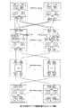
図1は、本発明の実施形態に係るディスク制御装置の全体構成を示す図である。本実施形態に係るディスク制御装置は、ホストコンピュータ又はディスクドライブ装置との接続インターフェース140を持つチャネルアダプタ100と、ホストコンピュータとディスクドライブ装置の間で転送されるデータを一時的に格納するメモリアダプタ300と、チャネルアダプタ100及びメモリアダプタ300の動作を制御するプロセッサアダプタ200と、チャネルアダプタ100、メモリアダプタ300、プロセッサアダプタ200の間を接続して内部ネットワークを構成するためのスイッチアダプタ400と、を備えている。 FIG. 1 is a diagram showing an overall configuration of a disk control apparatus according to an embodiment of the present invention. The disk controller according to this embodiment includes a
また、チャネルアダプタ100、プロセッサアダプタ200、メモリアダプタ300、スイッチアダプタ400が、内部ネットワークの通信プロトコル制御を行うDMAコントローラ(DMAC)120、220、320、420をそれぞれ有している。各DMACは、データリンクエンジン(DLE)110、210、310、410を介して、DMA転送を実行する。これらのDMAコントローラ間では、図11に示すコネクションレス型パケット多重通信が行われる。 In addition, the
図11は本発明の実施形態にディスク制御装置に用いられる多重通信転送プロトコルを示す図である。図11において、或る分割DMAリクエストに対する分割ステータスの確認を待たずに、次の分割DMAリクエストが発行されている(多重通信、すなわち、1つの分割DMA転送の中での多重通信)。さらに、DMA1とDMA2の間のDMA転送とDMA3とDMA4との間のDMA転送が同じDLE1−DLE2間のパスを共有して行われている(コネクションレス型通信)。図11の例示で云うと、分割DMA615と分割DMA616がDLE1−DLE2間のパスを共有して交互に転送されて多重通信を行っている。そして、後述する図8の説明で明らかになるように、宛先とデータと分割DMAリクエストの順序制御を行う情報(TASK ID)を含んだパケット構造を採用することによって、上述したコネクションレス型の多重通信を行うことが可能となるのである。 FIG. 11 is a diagram showing a multiplex communication transfer protocol used in the disk controller according to the embodiment of the present invention. In FIG. 11, the next divided DMA request is issued without waiting for confirmation of the division status for a certain divided DMA request (multiplex communication, that is, multiple communication in one divided DMA transfer). Further, DMA transfer between DMA1 and DMA2 and DMA transfer between DMA3 and DMA4 are performed by sharing the same path between DLE1 and DLE2 (connectionless communication). In the example of FIG. 11, the divided
図1及び図11に示す構成例によれば、コネクションレス型多重通信を適用することによって、1つの分割DMA転送の中だけでなく、複数のDMA転送の間でも多重化することが可能となり、パス利用効率が飛躍的に改善されて(パスに時間間隔を空けることなくデータ転送できるのでパス効率が向上する)、従来技術で設けられていた制御系内部ネットワークとデータ系内部ネットワークを別設する必然性がなくなる。そのため、キャッシュメモリアダプタと制御メモリアダプタを統合してメモリアダプタとし、さらに、パスの利用制限が緩和されたことによってプロセッサをプロセッサアダプタとしてチャネルアダプタから独立させることが可能となる。これにより、より拡張性、柔軟性にすぐれた低コストのディスク制御装置を構成することが可能となる。 According to the configuration example shown in FIGS. 1 and 11, by applying connectionless multiplex communication, it is possible to multiplex not only within one divided DMA transfer but also between a plurality of DMA transfers, The path utilization efficiency has been drastically improved (data can be transferred without leaving a time interval in the path, thus improving the path efficiency), and the control system internal network and the data system internal network provided in the prior art are provided separately. There is no necessity. For this reason, the cache memory adapter and the control memory adapter are integrated to form a memory adapter, and further, the use of the path is relaxed, so that the processor can be made independent from the channel adapter as a processor adapter. As a result, it is possible to configure a low-cost disk control device with more extensibility and flexibility.
次に、図5は本発明の実施形態に係るディスク制御装置におけるプロセッサアダプタの具体的構成例を示す図であり、図2はプロセッサアダプタに用いられるデータリンクエンジンの具体的構成例を示す図である。なお、図2のデータリンクエンジン(DLE)はプロセッサアダプタに限らず、他のアダプタにも使用される構成例である。 Next, FIG. 5 is a diagram showing a specific configuration example of the processor adapter in the disk controller according to the embodiment of the present invention, and FIG. 2 is a diagram showing a specific configuration example of the data link engine used in the processor adapter. is there. The data link engine (DLE) in FIG. 2 is a configuration example that is used not only for the processor adapter but also for other adapters.
図5に示すプロセッサアダプタ200は、マイクロプロセッサ(MP)230と複数のDMAコントローラ220と1つ以上のデータリンクエンジン(DLE)210とを有し、MP230とDMAC220の間がセレクタ225によって接続され、複数のDMAコントローラ220がセレクタ215を通してDLE210を共有している。すなわち、DLEの数よりもDMACの数の方がはるかに多いのが通常である。 A
複数のDMAコントローラ220からのリクエストはセレクタ215内のDMAC調停回路2150によって調停されることで、同じDLE210を介して複数のDMACからのDMA転送を同時に実行すること(コネクションレス通信)が可能となっている。DLE210からの受信データは、DLE調停回路2155によって、目的のDMAC220に分配される。 Requests from a plurality of
図2において、DLEは、送信ポート1101と送信バッファ1102と受信ポート1105と受信バッファ1106と再送論理回路1110と再送バッファ1120とから構成されている。再送バッファと再送論理回路は、データリンクでのエラーフリー転送を実現するための処理を実行する。すなわち、送信バッファから送信ポートを通して送出されたパケットは、再送論理回路1110によって再送バッファ1120に格納される。受信ポートには、当該パケットが正しく届いたかどうかのステータスが返送され、エラーが報告された場合、再送論理回路により再送バッファからパケットの再送が行われる。図2に示すDLE構成により、パケット単位のデータリンクエラー制御が可能となり、多重通信を実現することができる。 In FIG. 2, the DLE includes a
図5及び図2に示す構成例によれば、コネクションレス型の多重通信が可能となり、高性能で、より柔軟かつ単純な低コストのディスク制御装置を実現することができる。 According to the configuration example shown in FIGS. 5 and 2, connectionless multiplex communication is possible, and a high-performance, more flexible and simple low-cost disk controller can be realized.
次に、図4は本発明の実施形態に係るディスク制御装置におけるチャネルアダプタの具体的構成例を示す図であり、図3はチャネルアダプタに用いられるDMAコントローラの具体的構成例を示す図である。なお、図3のDMAコントローラ(DMAC)はチャネルアダプタに限らず、他のアダプタにも使用される構成例である。 Next, FIG. 4 is a diagram showing a specific configuration example of the channel adapter in the disk controller according to the embodiment of the present invention, and FIG. 3 is a diagram showing a specific configuration example of the DMA controller used in the channel adapter. . The DMA controller (DMAC) in FIG. 3 is a configuration example that is used not only for the channel adapter but also for other adapters.
図4に示すチャネルアダプタは、プロトコルエンジン130と、DMAC120と、DLE110と、を備え、PE130とDMAC120がセレクタ125を通して接続され、DMAC120とDLE110がセレクタ115を介して接続されている。DMAコントローラ120が、複数(VC0、VC1)の受信FIFOバッファと複数(VC0、VC1)の送信FIFOバッファを持っている。 The channel adapter shown in FIG. 4 includes a
図3に示すDMAコントローラ120は、マルチプレクサ1201と、送信FIFOバッファ1202と、デマルチプレクサ1205と、受信FIFOバッファ1206と、トランザクション論理回路1210と、シーケンス管理テーブル1220と、パケット生成論理回路1230と、パケット分解論理回路1240と、から構成されている。複数の送信FIFOバッファ1202の間で送信データ間の競合が調停回路1212により調停されマルチプレクサ1201によって選択される。 The
同様に、受信データは、調停回路1212の制御によるデマルチプレクサ1205の選択動作によって、複数の受信FIFOバッファ1206の中の適当なFIFOに格納される。パケット生成論理回路1230とパケット分解論理回路1240は、パケットの生成と分解を行うための論理回路である。シーケンス制御論理回路1213とシーケンス管理テーブル1220は、分割DMAのDMAシーケンスを管理するための論理回路であり、その動作については後述する。 Similarly, the received data is stored in an appropriate FIFO in the plurality of receive FIFO buffers 1206 by the selection operation of the
図4及び図3に示す構成例によれば、1つのDLEに対して、複数(VC0、VC1)のバッファを対応させることができ、例えば、制御系内部ネットワークとデータ系内部ネットワークを1つのDLEに混在させることができる(例として、VCOはデータ系内部ネットワーク用、VC1は制御系ネットワーク用)。さらに、調停回路1212の動作により、複数のバッファ間に優先度を設けることができ、例えば、制御系内部ネットワークをデータ系内部ネットワークより優先させることにより、両者の混在による制御系内部ネットワークのアクセス遅延時間増大を回避することができる。すなわち、本構成例により、より単純な内部ネットワーク構成のディスク制御装置を実現することが可能となり、性能改善と低コスト化の両立を実現することができる。 According to the configuration example shown in FIGS. 4 and 3, a plurality of (VC0, VC1) buffers can be associated with one DLE. For example, a control system internal network and a data system internal network are connected to one DLE. (For example, VCO is for the data system internal network and VC1 is for the control system network.) Furthermore, priority can be provided between a plurality of buffers by the operation of the
次に、図6は本発明の実施形態に係るディスク制御装置におけるメモリアダプタの具体的構成例を示す図である。図6に示すメモリアダプタは、メモリモジュール(MM)340と、メモリコントローラ(MC)330と、DMAC320と、DLE310と、を備え、MC330とDMAC320がセレクタ325を通して接続され、DMAC320とDLE310がセレクタ315を介して接続されている。DMAコントローラ(DMAC)320が、それぞれ受信FIFOバッファ(VC0またはVC1)と送信FIFOバッファ(VC0またはVC1)を持っている。複数の送信FIFOバッファVC0の間及び複数の送信FIFOバッファVC1の間で送信データ間の競合が調停されて、DLE310にデータが送信される。同様に、複数の受信FIFOバッファVC0の間及び複数の受信FIFOバッファVC1の間で受信データ間の経路調停がなされて、適当な受信FIFOにデータが格納される。 Next, FIG. 6 is a diagram showing a specific configuration example of the memory adapter in the disk controller according to the embodiment of the present invention. The memory adapter shown in FIG. 6 includes a memory module (MM) 340, a memory controller (MC) 330, a
また、DMAC320とMC330との間は、調停回路3250と調停回路3255によって、競合条件が調停される。これにより、1つのMCを複数のDMACで共有することができ、調停回路の機能として、DMAC間での優先度制御を実現することも可能となる。これにより、例えば、制御系内部ネットワーク用のDMACとデータ系内部ネットワーク用のDMACを設けて、制御系内部ネットワーク用のDMACを優先させることにより、制御系内部ネットワークのアクセスがデータ系内部ネットワークの動作に干渉される影響を抑制することが可能となる。 In addition, the
図6に示す構成例によると、1つのDLEに対して、複数のDMACを対応させることができ、例えば、制御系内部ネットワークとデータ系内部ネットワークを1つのDLEに混在させることができる。また、1つのMCに対して、複数のDMACを対応させることができ、制御系メモリとデータ系メモリを混在させることが可能となる。すなわち、本構成例により、より単純な内部ネットワーク構成のディスク制御装置を実現することが可能となり、性能改善と低コスト化の両立を実現することができる。 According to the configuration example shown in FIG. 6, a plurality of DMACs can be associated with one DLE. For example, a control internal network and a data internal network can be mixed in one DLE. In addition, a plurality of DMACs can be associated with one MC, and a control system memory and a data system memory can be mixed. That is, according to this configuration example, a disk control device having a simpler internal network configuration can be realized, and both performance improvement and cost reduction can be realized.
次に、図8は本発明の実施形態に係るディスク制御装置内の複数のDMAコントローラ間で転送されるパケットの具体的構成例を示す図である。図8に示すパケット500は、転送先のDMAコントローラを指定するアドレスフィールド511と、転送元DMAコントローラを指定するアドレスフィールド521と、1つのDMA転送を複数のパケットに分割して転送する際の転送順序を管理するためのDMAシーケンスフィールド524と、を少なくとも備えている。 Next, FIG. 8 is a diagram showing a specific configuration example of a packet transferred between a plurality of DMA controllers in the disk controller according to the embodiment of the present invention. A
本発明の実施形態に係るディスク制御装置においては、コネクションレス型の多重通信によるDMA転送が行われるため、DMAの転送順序を保証し、エラーチェックや、障害処理を適切に行う必要がある。そのための手段として、パケットを確実に特定することができるようにDMAシーケンスフィールドを設け、このフィールドを、1つのDMA転送内においてユニークになる(識別できる)ように(好ましくは、シーケンシャルにインクリメント)制御する。 In the disk control apparatus according to the embodiment of the present invention, DMA transfer is performed by connectionless multiplex communication. Therefore, it is necessary to guarantee the DMA transfer order and appropriately perform error check and failure processing. As a means for this, a DMA sequence field is provided so that a packet can be reliably identified, and this field is controlled to be unique (identifiable) within one DMA transfer (preferably incremented sequentially). To do.
図8に示すパケット構成例によれば、コネクションレス型の多重通信によるDMA転送においても、適切な順序保証とそのチェックを行うことができ、また、障害発生時にも適切な障害処理を実施することが可能となる。すなわち、本構成例により、従来と同等の高信頼ディスク制御装置を実現することが可能となる。 According to the packet configuration example shown in FIG. 8, it is possible to perform an appropriate order guarantee and check even in DMA transfer by connectionless multiplex communication, and to perform appropriate failure processing even when a failure occurs. Is possible. That is, according to this configuration example, it is possible to realize a highly reliable disk control device equivalent to the conventional one.
また、図8に示したパケット500は、パケットの中継DMAコントローラを指定する第1のアドレス511と、宛先DMAコントローラを指定する第2のアドレス522及び第3のアドレス523と、宛先DMAコントローラに転送すべき転送データ531と、を備えている。チャネルアダプタ100からメモリアダプタ300へのWRITEリクエストの際は、第1のアドレスとしてスイッチアダプタのDMAC420が、第2及び第3のアドレスとしてメモリアダプタのDMAC320が指定される。複数のメモリアダプタのアドレスを指定するのは、信頼性向上を目指して、キャッシュメモリに対し2重WRITEを実施するためである。 Further, the
このようなパケット構成によって、2重WRITEを含んだDMA転送機能を、コネクションレス型の多重通信に適用することが可能となり、高信頼のディスク制御装置を実現することができる。 With such a packet configuration, a DMA transfer function including double WRITE can be applied to connectionless multiplex communication, and a highly reliable disk controller can be realized.
さらに、図8に示したパケット500は、DLEに対する制御情報を含んだルーティングヘッダ510と、DMAコントローラに対する制御情報を含んだコマンドヘッダ520と、それ以外のデータを含んだデータブロック530と、から構成され、ルーティングヘッダ510は、当該ルーティングヘッダ内の転送エラーを保証するためのルーティングヘッダエラーチェックコード515を有し、コマンドヘッダ520は、当該コマンドヘッダ内の転送エラーを保証するためのコマンドヘッダエラーチェックコード525を含み、データブロック530は、当該データブロック内の転送エラーを保証するためのデータブロックエラーチェックコード535を含んでいる。 Further, the
このようなパケット構成によって、ルーティング制御情報と、DMAC制御情報と、データ情報を別々のエラーチェックコードで保護することが可能となり、より細かなDMA転送制御と障害回復処理が行える。とくに、スイッチアダプタ経由の2重WRITE時などルーティング制御情報の書き換えが必要となる場合でも、エラーチェックコード再計算の範囲を最小限に限定することが可能とり、高信頼かつ高性能なディスク制御装置を実現することができる。 With such a packet configuration, routing control information, DMAC control information, and data information can be protected by different error check codes, and finer DMA transfer control and failure recovery processing can be performed. In particular, even when routing control information needs to be rewritten, such as during double WRITE via a switch adapter, the range of error check code recalculation can be limited to a minimum, and a highly reliable and high performance disk controller. Can be realized.
次に、図9は本発明の実施形態に係るディスク制御装置に用いられるパケットのフローを示す図であり、図10は本発明の実施形態に係るディスク制御装置に用いられるプロトコルを示す図である。図9及び図10の例示では、チャネルアダプタのDMAC120からスイッチアダプタのDMAC420に分割DMAリクエスト610を発行している。すなわち、分割DMAリクエスト610のパケットには、転送元アドレスフィールド521として、マスターDMAであるチャネルアダプタDMAC120が指定され、転送先アドレスフィールド511としては、スイッチアダプタDMAC420が指定されている。 Next, FIG. 9 is a diagram showing a flow of a packet used in the disk controller according to the embodiment of the present invention, and FIG. 10 is a diagram showing a protocol used in the disk controller according to the embodiment of the present invention. . In the example of FIG. 9 and FIG. 10, the divided
DMAコントローラ420は、DMAコントローラ120に、分割DMA転送リクエスト610に対応した分割終了ステータス621、622を返送する。分割終了ステータス621、622には、分割DMA転送リクエスト610に含まれていたDMAシーケンスフィールド524の情報が含まれており、DMAコントローラ120は、そのDMAシーケンスフィールドの情報を確認することで、分割DMA転送の転送順序の確認を行う。 The
図12は、本発明の実施形態に係るディスク制御装置に用いられる分割DMA送信時のDMAシーケンスフィールド更新フローを示す図であり、図13は本発明の実施形態に係るディスク制御装置に用いられる分割ステータス受信時のDMAシーケンスフィールド確認フローを示す図である。各DMACは、現在のDMAシーケンスフィールドの値を変数CURR_DMA_SEQに保持している。分割DMA送信時には、CURR_DMA_SEQをインクリメントしながら、各転送パケットのDMAシーケンスフィールド524に挿入する。また、各DMACは、次に戻ってくるべき分割DMAステータスの値を変数NEXT_DMA_SEQに保持している。分割DMAステータスが戻ってきたなら、そのDMAシーケンスの値を期待値と比較し、一致したならNEXT_DMA_SEQをインクリメントする。不一致の場合は、現在しかかり中の分割DMA転送リクエスト(NEXT_DMA_SEQからCURR_DMA_SEQまで)をキャンセルした後、プロセッサに障害通知を行う。 FIG. 12 is a diagram showing a DMA sequence field update flow at the time of divided DMA transmission used in the disk controller according to the embodiment of the present invention. FIG. 13 is a diagram of the division used in the disk controller according to the embodiment of the present invention. It is a figure which shows the DMA sequence field confirmation flow at the time of status reception. Each DMAC holds the value of the current DMA sequence field in a variable CURR_DMA_SEQ. At the time of divided DMA transmission, CURR_DMA_SEQ is incremented and inserted into the DMA sequence field 524 of each transfer packet. Each DMAC holds the value of the divided DMA status to be returned next in the variable NEXT_DMA_SEQ. If the divided DMA status returns, the value of the DMA sequence is compared with the expected value, and if they match, NEXT_DMA_SEQ is incremented. If they do not match, the divided DMA transfer request (from NEXT_DMA_SEQ to CURR_DMA_SEQ) that is currently in progress is canceled, and a failure notification is sent to the processor.
図9及び図10、図12及び図13に示す構成例によれば、分割DMA転送においても、DMAシーケンスフィールド524を用いて確実にDMA毎の転送順序の制御を行うことが可能となる。すなわち、本構成例によって、コネクションレス型の多重通信で、高信頼のディスク制御装置を実現することができる。 According to the configuration examples shown in FIGS. 9, 10, 12, and 13, it is possible to reliably control the transfer order for each DMA using the DMA sequence field 524 even in divided DMA transfer. That is, according to the present configuration example, a highly reliable disk control device can be realized by connectionless multiplex communication.
また、図9及び図10には、本発明の実施形態に係るディスク制御装置に用いられる2重WRITEのパケットフロー(プロトコル)を示してある。本構成例では、チャネルアダプタDMAC120からスイッチアダプタDMAC420を介してメモリアダプタのDMAC321、322に分割DMAリクエスト611、612を発行している。すなわち、分割DMAリクエスト610のパケットには、転送元アドレスフィールド521としてチャネルアダプタDMAC120が指定され、転送先アドレスフィールド511としてスイッチアダプタDMAC420が指定され、宛先フィールドとしてメモリアダプタDMAC321,322が指定され、データブロック(フィールド)531には、転送データが格納されている。 9 and 10 show a double WRITE packet flow (protocol) used in the disk controller according to the embodiment of the present invention. In this configuration example, the divided DMA requests 611 and 612 are issued from the
スイッチアダプタ内のDMAコントローラ420で、DMAC321を転送先アドレスフィールドに持ち、転送データ531を含んだ分割DMAリクエストパケット611と、DMAC322を転送先アドレスフィールドに持ち、転送データ531を含んだ分割DMAリクエストパケット612が生成され、それぞれの転送先アドレスにたいして転送が行われる。メモリアダプタのDMAC321、322では、分割DMAリクエスト611、612に対して、スイッチアダプタDMAC420を介してチャネルアダプタDMAC120に対し分割ステータス621、622を返送する。 The
図9及び図10の上述した構成例により、スイッチアダプタのDMACによるキャッシュメモリ2重WRITEが実現できる。メモリアダプタ300に近接したスイッチアダプタ400のDMAC420で2重WRITEのためのパケットを生成するので、内部ネットワーク内の帯域を浪費することがなく、パス効率を向上させることができる。すなわち、本構成例例により、高性能かつ高信頼なディスク制御装置を実現することが可能となる。 With the above-described configuration examples of FIGS. 9 and 10, cache memory dual WRITE by the switch adapter DMAC can be realized. Since the packet for double WRITE is generated by the
次に、図7は、本発明の実施形態に係るディスク制御装置におけるスイッチアダプタの具体的構成例を示す図である。図7に示すスイッチアダプタは、複数のDLE410と複数のDMAC420とセレクタ430とを備えている。受信側DLE410から受信されたパケットは、受信側DMAC420の中で複数の受信FIFOバッファ(VC0,VC1)に分けて格納された後、送信FIFOバッファ間毎に存在するセレクタ論理回路4301、4302、4306、4307を通して、送信側DMAC420内の送信FIFOに送られ、送信側DLE410から送出される。 Next, FIG. 7 is a diagram showing a specific configuration example of the switch adapter in the disk controller according to the embodiment of the present invention. The switch adapter shown in FIG. 7 includes a plurality of
図7に示す構成例では、図8に示すルーティング制御情報、DMAC制御情報及びデータ情報を有するパケットと同様に、複数のDMAコントローラ間で転送されるパケットが、パケット制御情報を介して、宛先のDMAC情報を含んだヘッダ部と、それ以外のデータを含んだデータ部とから構成されており、ヘッダ部は、当該ヘッダ部内の転送エラーを保証するためのヘッダ部エラーチェックコードを含み、データ部は、当該データ部内の転送エラーを保証するためのデータ部エラーチェックコードを含んでいる。 In the configuration example shown in FIG. 7, as in the packet having the routing control information, the DMAC control information, and the data information shown in FIG. 8, a packet transferred between a plurality of DMA controllers is transmitted via the packet control information. The header portion includes DMAC information and a data portion including other data. The header portion includes a header portion error check code for guaranteeing a transfer error in the header portion, and includes a data portion. Includes a data part error check code for guaranteeing a transfer error in the data part.
スイッチアダプタ内の受信側DMAコントローラ420は、ヘッダ部エラーチェックコードを確認するまでは、パケットを送信側DMACに送らない。ヘッダ部エラーチェックコードを確認した後、パケットのヘッダ部とデータ部が、送信側DMACに対してパイプライン処理的に送られる。また、ヘッダ部エラーチェックコードでエラーが見つかった場合は、そのパケットを破棄し、しかるべきエラー処理を実行する。 The reception
図7に示す構成例により、スイッチアダプタは、受信DLEからすべてのデータ部を取り込んで、データ部エラーチェックコードを確認する前に、送信DLEからの送信処理を始める事ができるとともに、ヘッダ部にエラーが生じて宛先の不正となったパケットに対しては、パケット転送を破棄することによってエラーの伝播を抑制することが可能となる。すなわち、本構成例により、高性能かつ高信頼なディスク制御装置を実現することが可能となる。 With the configuration example shown in FIG. 7, the switch adapter can start the transmission process from the transmission DLE before fetching all the data parts from the reception DLE and confirming the data part error check code, and in the header part. It is possible to suppress error propagation by discarding a packet transfer for a packet whose destination is illegal due to an error. That is, according to this configuration example, a high-performance and highly reliable disk control device can be realized.
また、図4に示すチャネルアダプタ、図5に示すプロセッサアダプタのように、本発明の実施形態に係るディスク制御装置に用いられるアダプタでは、複数のDMACが複数のDLEを共有する構成をとっている。図4のチャネルアダプタを例にすると、DLEが2個でDMACが16個設けられて、各DMACが数の少ないDLEを共有するという状況が考えられる。この冗長構成により、例えば、DMACが或るDLEを介してDMA通信していた際に当該DLEに障害が発生した場合でも、DMAC調停回路1150(図4参照)または2150(図5参照)で経路制御することにより、別のDLEと接続し直すことが可能となる。同様に、複数のDMACの処理を、DMAC調停回路1150または2150で経路制御することにより、複数のDLE間に割り振って、負荷分散を実現することも可能となる。 Further, like the channel adapter shown in FIG. 4 and the processor adapter shown in FIG. 5, the adapter used in the disk controller according to the embodiment of the present invention has a configuration in which a plurality of DMACs share a plurality of DLEs. . Taking the channel adapter of FIG. 4 as an example, a situation is considered in which two DLEs and 16 DMACs are provided, and each DMAC shares a small number of DLEs. With this redundant configuration, for example, even when a failure occurs in the DLE when the DMAC is performing DMA communication via a certain DLE, the path is routed by the DMAC arbitration circuit 1150 (see FIG. 4) or 2150 (see FIG. 5). By controlling, it becomes possible to reconnect to another DLE. Similarly, a plurality of DMAC processes are routed by the
ただし、本構成例の調停回路1150及び2150は、同じDMACからの一連の分割DMAリクエストと分割ステータスについては、同じDLEから送受信するように制御する。より好ましくは、同じDMACからのリクエストとステータスについては、通常動作の送受信DLEを固定する。 However, the
図4と図5に示すような構成例により、一連の分割DMAリクエストと分割ステータスの内部ネットワーク経路が固定され、経路の相違による順序の入れ替え(追い越し)の可能性がなくなり、分割DMAリクエストと分割ステータスの順序制御を著しく容易にする。すなわち、本構成例によって、高信頼なディスク制御装置を容易に実現することが可能となる。 4 and FIG. 5, the internal network path of a series of divided DMA requests and division status is fixed, and there is no possibility of changing the order (overtaking) due to the difference in the paths. Significantly facilitates status sequence control. That is, according to this configuration example, a highly reliable disk control device can be easily realized.
次に、図14は本発明の他の実施形態に係るディスク制御装置の全体構成を示す図である。図14に示す本発明の他の実施形態では、複数のチャネルアダプタ100と複数のプロセッサアダプタ200と複数のメモリアダプタ300とが、複数のスイッチアダプタ400によって接続されている。すべてのアダプタ間に複数のパスを設けることにより、任意の一点障害を救済できる冗長性を実現することができる。各アダプタの接続態様は図14に図示する通りであり、それぞれのアダプタは、対応している2つのアダプタに対してそれぞれのパスを設けている。 Next, FIG. 14 is a diagram showing an overall configuration of a disk control apparatus according to another embodiment of the present invention. In another embodiment of the present invention shown in FIG. 14, a plurality of
本発明の他の実施形態によって、ディスク制御装置のシステムとしての冗長性を高めることで、信頼性を向上させることが可能となる。 According to another embodiment of the present invention, it is possible to improve the reliability by increasing the redundancy of the disk controller as a system.
さらに、図15は本発明の更に他の実施形態に係るディスク制御装置の全体構成を示す図である。図15に示す本発明の更に他の実施形態では、図14に示す本発明の他の実施形態に係るディスク制御装置2つを、そのスイッチアダプタの拡張ポート同士を接続させることにより、ディスク制御装置全体として拡張した構成をとる。この接続態様により、チャネルアダプタ、プロセッサアダプタ、メモリアダプタを増設することができ、同一のアーキテクチャでシステムのスケーラビリティを向上させている。すなわち、本発明の更に他の実施形態により、ディスク制御装置のスケーラビリティを改善することが可能となる。 FIG. 15 is a diagram showing the overall configuration of a disk control apparatus according to still another embodiment of the present invention. In still another embodiment of the present invention shown in FIG. 15, two disk control devices according to another embodiment of the present invention shown in FIG. 14 are connected to each other by connecting expansion ports of their switch adapters. It takes an expanded configuration as a whole. With this connection mode, channel adapters, processor adapters, and memory adapters can be added, and the scalability of the system is improved with the same architecture. That is, the scalability of the disk control device can be improved according to still another embodiment of the present invention.
以上説明したように、図1〜図15に図示するような本発明の実施形態に係るディスク制御装置を採用すると、次に示すような機能や効果を奏させることが可能となる。すなわち、本実施形態によれば、1つのDLEに対して、複数のバッファを対応させることができ、例えば、制御系内部ネットワークとデータ系内部ネットワークを1つのDLEに混在させることができる。さらに、調停回路の動作により、複数のバッファ間に優先度を設けることができ、例えば、制御系内部ネットワークをデータ系内部ネットワークより優先させることにより、両者の混在による制御系内部ネットワークのアクセス遅延時間増大を回避することができる。これにより、より単純な内部ネットワーク構成のディスク制御装置を実現することが可能となり、性能改善と低コスト化の両立を実現することができる。 As described above, when the disk control device according to the embodiment of the present invention as shown in FIGS. 1 to 15 is employed, the following functions and effects can be achieved. That is, according to the present embodiment, a plurality of buffers can be associated with one DLE. For example, a control system internal network and a data system internal network can be mixed in one DLE. Furthermore, priority can be provided between a plurality of buffers by the operation of the arbitration circuit. For example, by giving priority to the control system internal network over the data system internal network, the access delay time of the control system internal network due to the mixture of both An increase can be avoided. As a result, it is possible to realize a disk control device having a simpler internal network configuration, and it is possible to achieve both performance improvement and cost reduction.
また、本実施形態によれば、1つのDLEに対して、複数のDMACを対応させることができ、例えば、制御系内部ネットワークとデータ系内部ネットワークを1つのDLEに混在させることができる。また、1つのMCに対して、複数のDMACを対応させることができ、制御系メモリとデータ系メモリを混在させることが可能となる。これにより、より単純な内部ネットワーク構成のディスク制御装置を実現することが可能となり、性能改善と低コスト化の両立を実現することができる。 Further, according to the present embodiment, a plurality of DMACs can be associated with one DLE. For example, a control system internal network and a data system internal network can be mixed in one DLE. In addition, a plurality of DMACs can be associated with one MC, and a control system memory and a data system memory can be mixed. As a result, it is possible to realize a disk control device having a simpler internal network configuration, and it is possible to achieve both performance improvement and cost reduction.
また、本実施形態によれば、コネクションレス型の多重通信によるDMA転送においても、適切な順序保証とそのチェックを行うことができ、また、障害発生時にも適切な障害処理を実施することが可能で、従来と同等の高信頼ディスク制御装置を実現することができる。また、本実施形態によれば、ルーティング制御情報と、DMAC制御情報と、データ情報を別々のエラーチェックコードで保護することが可能となり、より細かなDMA転送制御と障害回復処理が行える。特に、スイッチアダプタ経由の2重WRITE時などルーティング制御情報の書き換えが必要となる場合でも、エラーチェックコード再計算の範囲を最小限に限定することが可能とり、高信頼かつ高性能なディスク制御装置を実現することができる。 Further, according to the present embodiment, it is possible to perform appropriate order guarantee and check even in DMA transfer by connectionless multiplex communication, and it is possible to perform appropriate failure processing even when a failure occurs. Thus, a highly reliable disk control device equivalent to the conventional one can be realized. Further, according to the present embodiment, routing control information, DMAC control information, and data information can be protected with separate error check codes, and finer DMA transfer control and failure recovery processing can be performed. In particular, even when it is necessary to rewrite the routing control information during double WRITE via a switch adapter, the range of error check code recalculation can be limited to a minimum, and a highly reliable and high performance disk controller. Can be realized.
また、本実施形態によれば、スイッチアダプタのDMACによるキャッシュメモリ2重WRITEが実現できる。キャッシュメモリアダプタに近接したスイッチアダプタのDMACで2重WRITEのためのパケットを生成するので、内部ネットワーク内の帯域を浪費することがなく、パス効率を向上させることができる。 Further, according to the present embodiment, it is possible to realize a cache memory double WRITE by the switch adapter DMAC. Since the packet for the double WRITE is generated by the DMAC of the switch adapter close to the cache memory adapter, the bandwidth in the internal network is not wasted and the path efficiency can be improved.
また、本実施形態によれば、スイッチアダプタは、受信DLEからすべてのデータ部を取り込んでデータ部エラーチェックコードを確認する前に、送信DLEからの送信処理を始めることができるとともに、ヘッダ部にエラーが生じて宛先の不正となったパケットに対しては、パケット転送を破棄することによってエラーの伝播を抑制することが可能となる。また、本実施形態によれば、一連の分割DMAリクエストと分割ステータスの内部ネットワーク経路が固定され、経路の相違による順序の入れ替え(追い越し)の可能性がなくなり、分割DMAリクエストと分割ステータスの順序制御を著しく容易にする。 In addition, according to the present embodiment, the switch adapter can start the transmission process from the transmission DLE before taking in all the data parts from the reception DLE and confirming the data part error check code, and in the header part. It is possible to suppress error propagation by discarding a packet transfer for a packet whose destination is illegal due to an error. In addition, according to the present embodiment, the internal network path of a series of divided DMA requests and division status is fixed, and there is no possibility of order change (overtaking) due to the difference in path, and the order control of divided DMA requests and division statuses is eliminated. Makes it significantly easier.
また、本実施形態によれば、ディスク制御装置のシステムとして冗長性を持たせることで、信頼性を向上させることが可能となる。また、本実施形態によれば、ディスク制御装置のスケーラビリティを改善することが可能となる。 Further, according to the present embodiment, it is possible to improve reliability by providing redundancy as a system of the disk control device. Further, according to the present embodiment, it is possible to improve the scalability of the disk control device.
100 チャネルアダプタ
110,210,310,410 データリンクエンジン
115,125,215,225、315,325,430 セレクタ
120,220,320,321,322,420 DMAコントローラ
130 プロトコルエンジン
200 プロセッサアダプタ
230 マイクロプロセッサ
300 メモリアダプタ
330 メモリコントローラ
340 メモリモジュール
400 スイッチアダプタ
500 転送パケット
510 ルーティングヘッダ部
511 転送先アドレスフィールド
520 コマンドヘッダ部
521 転送元アドレスフィールド
522,523 DMA宛先アドレス
524 DMAシーケンスフィールド
530 データブロック部
600 DMAリスト
610,611,612,615,616 分割DMAリクエスト
621,622,625,626 分割ステータス
630 完了ステータス100
Claims (15)
Translated fromJapanese前記チャネルアダプタ、前記メモリアダプタ、前記プロセッサアダプタ、及び前記スイッチアダプタは、前記内部ネットワークの通信プロトコル制御を行うDMAコントローラを有し、
各アダプタに設けられた前記DMAコントローラの間でパケット多重通信を行う
ことを特徴とするディスク制御装置。A channel adapter having a connection interface with a host computer or a disk drive device, a memory adapter for temporarily storing data transferred between the host computer and the disk drive device, and operations of the channel adapter and the memory adapter A processor adapter that controls the channel adapter, the memory adapter, and a switch adapter that connects the processor adapters to form an internal network,
The channel adapter, the memory adapter, the processor adapter, and the switch adapter each have a DMA controller that performs communication protocol control of the internal network,
A disk control device that performs packet multiplex communication between the DMA controllers provided in each adapter.
前記チャネルアダプタ、前記メモリアダプタ、前記プロセッサアダプタ及び前記スイッチアダプタは、それぞれ複数のDMAコントローラと1つ以上のデータリンクエンジンを有し、
複数の前記DMAコントローラは前記データリンクエンジンを共有しており、複数の前記DMAコントローラは前記データリンクエンジンを介してDMA転送を同時に実行する
ことを特徴とするディスク制御装置。In claim 1,
The channel adapter, the memory adapter, the processor adapter, and the switch adapter each have a plurality of DMA controllers and one or more data link engines.
The plurality of DMA controllers share the data link engine, and the plurality of DMA controllers simultaneously execute DMA transfer via the data link engine.
前記DMAコントローラは、複数の受信FIFOバッファと複数の送信FIFOバッファを持ち、
複数の前記受信FIFOバッファの間で受信データ間の競合が調停され、複数の前記送信FIFOバッファの間で送信データ間の競合が調停される
ことを特徴とするディスク制御装置。In claim 1 or 2,
The DMA controller has a plurality of reception FIFO buffers and a plurality of transmission FIFO buffers,
A disk control device, wherein contention between received data is arbitrated among the plurality of reception FIFO buffers, and contention between transmission data is arbitrated between the plurality of transmission FIFO buffers.
前記DMAコントローラは、受信FIFOバッファと送信FIFOバッファを持ち、
複数の前記DMAコントローラに属するそれぞれの前記受信FIFOバッファの間で受信データ間の競合が調停され、複数の前記DMAコントローラに属するそれぞれの前記送信FIFOバッファの間で送信データ間の競合が調停される
ことを特徴とするディスク制御装置。In claim 1 or 2,
The DMA controller has a reception FIFO buffer and a transmission FIFO buffer,
Competition between received data is arbitrated among the respective reception FIFO buffers belonging to the plurality of DMA controllers, and competition between transmission data is arbitrated between the respective transmission FIFO buffers belonging to the plurality of DMA controllers. A disk controller characterized by that.
前記チャネルアダプタ、前記メモリアダプタ、前記プロセッサアダプタ及び前記スイッチアダプタは、それぞれ、前記内部ネットワークの通信プロトコル制御を行う複数のDMAコントローラと、前記DMAコントローラによって共有される1つ以上のデータリンクエンジンと、を有し、
前記DMAコントローラが複数の受信FIFOバッファと送信FIFOバッファを有することで、1つのデータリンクエンジンに対して複数のバッファを対応させ、
複数の前記DMAコントローラに属するそれぞれの前記受信FIFOバッファの間で受信データ間の競合が調停され、複数の前記DMAコントローラに属するそれぞれの前記送信FIFOバッファの間で送信データ間の競合が調停されることで、複数のバッファ間に優先度を設け、
1つのデータリンクエンジンに制御系の内部ネットワークとデータ系の内部ネットワークを混在させて、各アダプタに設けられた前記DMAコントローラの間でパケット多重通信を行う
ことを特徴とするディスク制御装置。A channel adapter having a connection interface with a host computer or a disk drive device, a memory adapter for temporarily storing data transferred between the host computer and the disk drive device, and operations of the channel adapter and the memory adapter A processor adapter that controls the channel adapter, the memory adapter, and a switch adapter that connects the processor adapters to form an internal network,
Each of the channel adapter, the memory adapter, the processor adapter, and the switch adapter includes a plurality of DMA controllers that perform communication protocol control of the internal network, and one or more data link engines shared by the DMA controllers; Have
Since the DMA controller has a plurality of reception FIFO buffers and a transmission FIFO buffer, a plurality of buffers are associated with one data link engine,
Competition between received data is arbitrated among the respective reception FIFO buffers belonging to the plurality of DMA controllers, and competition between transmission data is arbitrated between the respective transmission FIFO buffers belonging to the plurality of DMA controllers. By setting a priority between multiple buffers,
A disk controller characterized by mixing a control internal network and a data internal network in one data link engine, and performing packet multiplex communication between the DMA controllers provided in each adapter.
前記チャネルアダプタ、前記メモリアダプタ、前記プロセッサアダプタ、及び前記スイッチアダプタは、前記内部ネットワークの通信プロトコル制御を行うDMAコントローラを有するディスク制御装置であって、
各アダプタの前記DMAコントローラ間で転送されるパケットは、転送先のDMAコントローラを指定するアドレスフィールドと、転送元のDMAコントローラを指定するアドレスフィールドと、1つのDMA転送を複数のパケットに分割して転送する際の転送順序を管理するDMAシーケンスフィールドと、を有し、
前記DMAシーケンスフィールドは、1つのDMA転送内においてユニークなタスクIDを持つ
ことを特徴とするディスク制御装置。A channel adapter having a connection interface with a host computer or a disk drive device, a memory adapter for temporarily storing data transferred between the host computer and the disk drive device, and operations of the channel adapter and the memory adapter A processor adapter that controls the channel adapter, the memory adapter, and a switch adapter that connects the processor adapters to form an internal network,
The channel adapter, the memory adapter, the processor adapter, and the switch adapter are disk control devices having a DMA controller that performs communication protocol control of the internal network,
A packet transferred between the DMA controllers of each adapter is divided into an address field for designating a transfer destination DMA controller, an address field for designating a transfer source DMA controller, and one DMA transfer into a plurality of packets. A DMA sequence field for managing the transfer order when transferring,
The disk control apparatus, wherein the DMA sequence field has a unique task ID within one DMA transfer.
各アダプタのDMAコントローラ間で転送されるパケットは、前記パケットの中継DMAコントローラを指定する第1のアドレスと、宛先DMAコントローラを指定する第2及び第3のアドレスと、前記宛先DMAコントローラに転送すべき転送データと、を持つ
ことを特徴とするディスク制御装置。In claim 6,
The packet transferred between the DMA controllers of each adapter is transferred to the first DMA address specifying the relay DMA controller of the packet, the second and third addresses specifying the destination DMA controller, and the destination DMA controller. A disk controller characterized by having transfer data to be transmitted.
前記チャネルアダプタ、前記メモリアダプタ、前記プロセッサアダプタ及び前記スイッチアダプタは、それぞれ複数のDMAコントローラと1つ以上のデータリンクエンジンを有し、
各アダプタのDMAコントローラ間で転送されるパケットは、前記データリンクエンジンに対する制御情報を含んだルーティング部と、前記DMAコントローラに対する制御情報を含んだコマンド部と、それ以外のデータを含んだデータ部と、から構成され、
前記ルーティング部は当該ルーティング部内の転送エラーを保証するためのルーティング部エラーチェックコードを含み、前記コマンド部は当該コマンド部内の転送エラーを保証するためのコマンド部エラーチェックコードを含み、前記データ部は当該データ部内の転送エラーを保証するためのデータ部エラーチェックコードを含む
ことを特徴とするディスク制御装置。In claim 6 or 7,
The channel adapter, the memory adapter, the processor adapter, and the switch adapter each have a plurality of DMA controllers and one or more data link engines.
A packet transferred between the DMA controllers of each adapter includes a routing unit including control information for the data link engine, a command unit including control information for the DMA controller, and a data unit including other data. Consists of
The routing unit includes a routing unit error check code for guaranteeing a transfer error in the routing unit, the command unit includes a command unit error check code for guaranteeing a transfer error in the command unit, and the data unit is A disk controller comprising a data part error check code for guaranteeing a transfer error in the data part.
前記転送元のアドレスフィールドで指定されたDMAコントローラから、前記転送先のアドレスフィールドで指定されたDMAコントローラに対して、分割DMA転送を行い、
前記転送先アドレスフィールドで指定されたDMAコントローラは、前記転送元アドレスフィールドで指定されたDMAコントローラに対して、前記分割したDMA転送に対応した分割終了ステータスを返送し、
前記分割終了ステータスは、前記分割したDMA転送に含まれていたDMAシーケンスフィールドの情報を有し、
前記転送元アドレスフィールドで指定されたDMAコントローラは、前記分割終了ステータスに含まれている前記DMAシーケンスフィールドの情報を確認することによって前記分割したDMA転送の転送順序の確認を行う
ことを特徴とするディスク制御装置。In claim 6, 7 or 8,
Perform a divided DMA transfer from the DMA controller specified in the transfer source address field to the DMA controller specified in the transfer destination address field,
The DMA controller specified in the transfer destination address field returns a division end status corresponding to the divided DMA transfer to the DMA controller specified in the transfer source address field,
The division end status includes information of a DMA sequence field included in the divided DMA transfer,
The DMA controller specified in the transfer source address field confirms the transfer order of the divided DMA transfers by confirming the information of the DMA sequence field included in the division end status. Disk controller.
前記DMAコントローラ間で転送されるパケットが、前記スイッチアダプタ内のDMAコントローラを指定する第1のアドレスと、宛先DMAコントローラを指定する第2及び第3のアドレスと、前記宛先DMAコントローラに転送すべき転送データと、を有する場合、
前記スイッチアダプタ内のDMAコントローラにおいて、前記第2のアドレスを前記転送先のアドレスフィールドに持ち且つ前記転送データを含んだパケットと、前記第3のアドレスを前記転送先のアドレスフィールドに持ち且つ前記転送データを含んだパケットと、を生成する
ことを特徴とするディスク制御装置。In any one of claims 6 to 9,
Packets transferred between the DMA controllers should be forwarded to the first address designating the DMA controller in the switch adapter, the second and third addresses designating the destination DMA controller, and the destination DMA controller Transfer data,
In the DMA controller in the switch adapter, the packet having the second address in the transfer destination address field and including the transfer data, and the third address in the transfer destination address field and the transfer A disk controller characterized by generating a packet including data.
各アダプタのDMAコントローラ間で転送されるパケットは、パケット制御情報を含んだヘッダ部と、それ以外のデータを含んだデータ部と、から構成され、
前記ヘッダ部は当該ヘッダ部内の転送エラーを保証するためのヘッダ部エラーチェックコードを含み、前記データ部は当該データ部内の転送エラーを保証するためのデータ部エラーチェックコードを含み、
前記スイッチアダプタ内のDMAコントローラは、ヘッダ部エラーチェックコードが正常なパケットのみを通過させる
ことを特徴とするディスク制御装置。In claim 6 or 7,
A packet transferred between the DMA controllers of each adapter is composed of a header portion including packet control information and a data portion including other data.
The header part includes a header part error check code for guaranteeing a transfer error in the header part, and the data part includes a data part error check code for guaranteeing a transfer error in the data part,
The disk controller according to claim 1, wherein the DMA controller in the switch adapter passes only a packet having a normal header error check code.
前記チャネルアダプタ、前記メモリアダプタ、前記プロセッサアダプタ及び前記スイッチアダプタは、複数のDMAコントローラと複数のデータリンクエンジンを有し、
前記DMAコントローラが前記データリンクエンジンを介してDMA転送を実行する際、1つのDMA転送内では同一のデータリンクエンジンを介して転送が行われる
ことを特徴とするディスク制御装置。In claim 1,
The channel adapter, the memory adapter, the processor adapter, and the switch adapter each include a plurality of DMA controllers and a plurality of data link engines.
The disk controller according to claim 1, wherein when the DMA controller executes a DMA transfer via the data link engine, the transfer is performed via the same data link engine within one DMA transfer.
前記一のディスク制御装置に備えられた前記一のチャネルアダプタ、前記一のメモリアダプタ、前記一のプロセッサアダプタ、及び前記一のスイッチアダプタと同様の構成である他のディスク制御装置と、を設け、
前記一のスイッチアダプタは、前記一の各アダプタに接続されるとともに前記他の各アダプタにも接続され、
前記他のスイッチアダプタは、前記他の各アダプタに接続されるとともに前記一の各アダプタにも接続される
ことを特徴とするディスク制御装置。One channel adapter having a connection interface with a host computer or a disk drive device, one memory adapter for temporarily storing data transferred between the host computer and the disk drive device, and the one channel adapter And one processor adapter that controls the operation of the one memory adapter, and one switch adapter that connects the one channel adapter, the one memory adapter, and the one processor adapter together to form an internal network The one channel adapter, the one memory adapter, the one processor adapter, and the one switch adapter each include a DMA controller that controls a communication protocol of the internal network, and is provided in each adapter. Said DMA core And one disk controller for performing packet multiplex communication between the controller,
Another disk controller having the same configuration as the one channel adapter, the one memory adapter, the one processor adapter, and the one switch adapter provided in the one disk controller;
The one switch adapter is connected to each of the one adapter and also to each of the other adapters,
The other switch adapter is connected to each of the other adapters as well as to each of the other adapters.
前記一のスイッチアダプタ及び/又は前記他のスイッチアダプタの拡張ポートに対して、更に他のスイッチアダプタの拡張ポートを接続する
ことを特徴とするディスク制御装置。In claim 13,
A disk controller, wherein an expansion port of another switch adapter is further connected to an expansion port of the one switch adapter and / or the other switch adapter.
前記チャネルアダプタ、前記メモリアダプタ、前記プロセッサアダプタ、及び前記スイッチアダプタは、前記内部ネットワークの通信プロトコル制御を行うDMAコントローラと、前記内部ネットワークとの間でDMA転送を実行するデータリンクエンジンと、を有し、
各アダプタに設けられた前記DMAコントローラの間で転送されるパケットは、転送先のDMAコントローラを指定するアドレスフィールドと、転送元のDMAコントローラを指定するアドレスフィールドと、1つのDMA転送を複数パケットに分割して転送する際の転送順序を管理するDMAシーケンスフィールドと、を備える
ことを特徴とするディスク制御装置。A channel adapter having a connection interface with a host computer or a disk drive device, a memory adapter for temporarily storing data transferred between the host computer and the disk drive device, and operations of the channel adapter and the memory adapter A processor adapter that controls the channel adapter, the memory adapter, and a switch adapter that connects the processor adapters to form an internal network,
The channel adapter, the memory adapter, the processor adapter, and the switch adapter each have a DMA controller that performs communication protocol control of the internal network and a data link engine that executes DMA transfer with the internal network. And
A packet transferred between the DMA controllers provided in each adapter includes an address field for designating a destination DMA controller, an address field for designating a source DMA controller, and one DMA transfer into a plurality of packets. A disk control device comprising: a DMA sequence field for managing a transfer order when divided and transferred.
Priority Applications (8)
| Application Number | Priority Date | Filing Date | Title |
|---|---|---|---|
| JP2004038459AJP4405277B2 (en) | 2004-02-16 | 2004-02-16 | Disk controller |
| US10/826,471US7231469B2 (en) | 2004-02-16 | 2004-04-16 | Disk controller |
| DE102004023810ADE102004023810B3 (en) | 2004-02-16 | 2004-05-13 | Disk controller |
| GB0411905AGB2411022B (en) | 2004-02-16 | 2004-05-27 | Disk controller |
| FR0405789AFR2866448B1 (en) | 2004-02-16 | 2004-05-28 | DISC CONTROLLER |
| US11/249,174US7467238B2 (en) | 2004-02-10 | 2005-10-11 | Disk controller and storage system |
| US11/652,567US7469307B2 (en) | 2004-02-16 | 2007-01-12 | Storage system with DMA controller which controls multiplex communication protocol |
| US12/269,152US7917668B2 (en) | 2004-02-10 | 2008-11-12 | Disk controller |
Applications Claiming Priority (1)
| Application Number | Priority Date | Filing Date | Title |
|---|---|---|---|
| JP2004038459AJP4405277B2 (en) | 2004-02-16 | 2004-02-16 | Disk controller |
Publications (3)
| Publication Number | Publication Date |
|---|---|
| JP2005228245Atrue JP2005228245A (en) | 2005-08-25 |
| JP2005228245A5 JP2005228245A5 (en) | 2006-11-16 |
| JP4405277B2 JP4405277B2 (en) | 2010-01-27 |
Family
ID=32677684
Family Applications (1)
| Application Number | Title | Priority Date | Filing Date |
|---|---|---|---|
| JP2004038459AExpired - Fee RelatedJP4405277B2 (en) | 2004-02-10 | 2004-02-16 | Disk controller |
Country Status (5)
| Country | Link |
|---|---|
| US (2) | US7231469B2 (en) |
| JP (1) | JP4405277B2 (en) |
| DE (1) | DE102004023810B3 (en) |
| FR (1) | FR2866448B1 (en) |
| GB (1) | GB2411022B (en) |
Cited By (7)
| Publication number | Priority date | Publication date | Assignee | Title |
|---|---|---|---|---|
| JP2009193282A (en)* | 2008-02-14 | 2009-08-27 | Sharp Corp | Data processing device |
| US7640365B2 (en) | 2006-09-26 | 2009-12-29 | Hitachi, Ltd. | Highly reliable disk controller |
| JP2010092336A (en)* | 2008-10-09 | 2010-04-22 | Hitachi Ltd | Storage system and communication method |
| US7831764B2 (en) | 2007-02-19 | 2010-11-09 | Hitachi, Ltd | Storage system having plural flash memory drives and method for controlling data storage |
| US7882136B2 (en) | 2007-05-23 | 2011-02-01 | Hitachi, Ltd. | Foresight data transfer type hierarchical storage system |
| JP2012103975A (en)* | 2010-11-11 | 2012-05-31 | Nec Computertechno Ltd | Data transfer device, data transfer method, and computer system |
| US8495288B2 (en) | 2008-04-02 | 2013-07-23 | Hitachi, Ltd. | Storage controller and duplicated data detection method using storage controller |
Families Citing this family (12)
| Publication number | Priority date | Publication date | Assignee | Title |
|---|---|---|---|---|
| US7958224B2 (en)* | 1999-02-17 | 2011-06-07 | Catalina Marketing Corporation | Incentive network for distributing incentives on a network-wide basis and for permitting user access to individual incentives from a plurality of network servers |
| KR100551480B1 (en)* | 2004-10-25 | 2006-02-13 | 삼성전자주식회사 | A memory device located between the processor and the nonvolatile memory, a system including the same, and a data transmission / reception method within the system |
| US7590885B2 (en)* | 2005-04-26 | 2009-09-15 | Hewlett-Packard Development Company, L.P. | Method and system of copying memory from a source processor to a target processor by duplicating memory writes |
| TWI347528B (en)* | 2005-09-23 | 2011-08-21 | Infortrend Technology Inc | Redundant storage virtualization subsystem and computer system having data path branching functionality and data-accessing method thereof |
| JP4446968B2 (en)* | 2006-02-22 | 2010-04-07 | シャープ株式会社 | Data processing device |
| JP4933284B2 (en)* | 2007-01-25 | 2012-05-16 | 株式会社日立製作所 | Storage apparatus and load balancing method |
| WO2010116538A1 (en)* | 2009-04-06 | 2010-10-14 | Hitachi, Ltd. | Storage apparatus and data transfer method |
| US8583847B2 (en) | 2010-12-09 | 2013-11-12 | Dell Products, Lp | System and method for dynamically detecting storage drive type |
| US9015519B2 (en)* | 2012-01-31 | 2015-04-21 | Symantec Corporation | Method and system for cluster wide adaptive I/O scheduling by a multipathing driver |
| US9135097B2 (en)* | 2012-03-27 | 2015-09-15 | Oracle International Corporation | Node death detection by querying |
| US9658975B2 (en) | 2012-07-31 | 2017-05-23 | Silicon Laboratories Inc. | Data transfer manager |
| US9501437B2 (en) | 2012-11-15 | 2016-11-22 | Empire Technology Development Llc | Scalable storage system having multiple storage channels |
Family Cites Families (102)
| Publication number | Priority date | Publication date | Assignee | Title |
|---|---|---|---|---|
| NL8004884A (en) | 1979-10-18 | 1981-04-22 | Storage Technology Corp | VIRTUAL SYSTEM AND METHOD FOR STORING DATA. |
| GB8626642D0 (en) | 1986-11-07 | 1986-12-10 | Nighthawk Electronics Ltd | Data buffer/switch |
| US5206943A (en)* | 1989-11-03 | 1993-04-27 | Compaq Computer Corporation | Disk array controller with parity capabilities |
| US5249279A (en)* | 1989-11-03 | 1993-09-28 | Compaq Computer Corporation | Method for controlling disk array operations by receiving logical disk requests and translating the requests to multiple physical disk specific commands |
| US5680574A (en)* | 1990-02-26 | 1997-10-21 | Hitachi, Ltd. | Data distribution utilizing a master disk unit for fetching and for writing to remaining disk units |
| US5140592A (en)* | 1990-03-02 | 1992-08-18 | Sf2 Corporation | Disk array system |
| US5166939A (en) | 1990-03-02 | 1992-11-24 | Micro Technology, Inc. | Data storage apparatus and method |
| US5201053A (en)* | 1990-08-31 | 1993-04-06 | International Business Machines Corporation | Dynamic polling of devices for nonsynchronous channel connection |
| US5440752A (en) | 1991-07-08 | 1995-08-08 | Seiko Epson Corporation | Microprocessor architecture with a switch network for data transfer between cache, memory port, and IOU |
| US5257391A (en)* | 1991-08-16 | 1993-10-26 | Ncr Corporation | Disk controller having host interface and bus switches for selecting buffer and drive busses respectively based on configuration control signals |
| JP2834927B2 (en) | 1992-02-28 | 1998-12-14 | 三菱電機株式会社 | Computer system |
| US5740465A (en)* | 1992-04-08 | 1998-04-14 | Hitachi, Ltd. | Array disk controller for grouping host commands into a single virtual host command |
| JPH0756693A (en) | 1993-08-13 | 1995-03-03 | Toshiba Corp | Disk array device and disk write controller |
| US5511227A (en)* | 1993-09-30 | 1996-04-23 | Dell Usa, L.P. | Method for configuring a composite drive for a disk drive array controller |
| JP3160448B2 (en)* | 1993-11-30 | 2001-04-25 | 富士通株式会社 | Data correction device |
| JPH07200187A (en) | 1993-12-30 | 1995-08-04 | Hitachi Ltd | Disk array device |
| JP3080827B2 (en) | 1994-01-27 | 2000-08-28 | 日本電気株式会社 | Multiplexing interface for file device and control method therefor |
| US5574950A (en)* | 1994-03-01 | 1996-11-12 | International Business Machines Corporation | Remote data shadowing using a multimode interface to dynamically reconfigure control link-level and communication link-level |
| US5548788A (en)* | 1994-10-27 | 1996-08-20 | Emc Corporation | Disk controller having host processor controls the time for transferring data to disk drive by modifying contents of the memory to indicate data is stored in the memory |
| US5729763A (en)* | 1995-08-15 | 1998-03-17 | Emc Corporation | Data storage system |
| US6355681B2 (en)* | 1995-12-07 | 2002-03-12 | Glytech, Inc. | Glycine substitutes and precursors for treating a psychosis |
| JP3776496B2 (en) | 1996-01-17 | 2006-05-17 | 株式会社日立製作所 | Data storage system |
| US5761534A (en)* | 1996-05-20 | 1998-06-02 | Cray Research, Inc. | System for arbitrating packetized data from the network to the peripheral resources and prioritizing the dispatching of packets onto the network |
| JPH10105347A (en) | 1996-10-02 | 1998-04-24 | Hitachi Ltd | Disk array control system |
| US5949982A (en)* | 1997-06-09 | 1999-09-07 | International Business Machines Corporation | Data processing system and method for implementing a switch protocol in a communication system |
| US6148349A (en)* | 1998-02-06 | 2000-11-14 | Ncr Corporation | Dynamic and consistent naming of fabric attached storage by a file system on a compute node storing information mapping API system I/O calls for data objects with a globally unique identification |
| US5974058A (en)* | 1998-03-16 | 1999-10-26 | Storage Technology Corporation | System and method for multiplexing serial links |
| JP3657428B2 (en)* | 1998-04-27 | 2005-06-08 | 株式会社日立製作所 | Storage controller |
| US6711632B1 (en)* | 1998-08-11 | 2004-03-23 | Ncr Corporation | Method and apparatus for write-back caching with minimal interrupts |
| JP4392877B2 (en) | 1998-09-18 | 2010-01-06 | 株式会社日立製作所 | Disk array controller |
| US6542961B1 (en)* | 1998-12-22 | 2003-04-01 | Hitachi, Ltd. | Disk storage system including a switch |
| JP4400895B2 (en)* | 1999-01-07 | 2010-01-20 | 株式会社日立製作所 | Disk array controller |
| JP4294142B2 (en)* | 1999-02-02 | 2009-07-08 | 株式会社日立製作所 | Disk subsystem |
| US6370605B1 (en)* | 1999-03-04 | 2002-04-09 | Sun Microsystems, Inc. | Switch based scalable performance storage architecture |
| JP2000298641A (en) | 1999-04-15 | 2000-10-24 | Nec Corp | Information processor, its data transferring method and storage medium with data transfer control program stored therein |
| US6330626B1 (en)* | 1999-05-05 | 2001-12-11 | Qlogic Corporation | Systems and methods for a disk controller memory architecture |
| US6401149B1 (en)* | 1999-05-05 | 2002-06-04 | Qlogic Corporation | Methods for context switching within a disk controller |
| US6542951B1 (en)* | 1999-08-04 | 2003-04-01 | Gateway, Inc. | Information handling system having integrated internal scalable storage system |
| JP4061563B2 (en)* | 1999-09-16 | 2008-03-19 | 松下電器産業株式会社 | Magnetic disk device, disk access method for magnetic disk device, and disk access control program recording medium for magnetic disk device |
| US6772108B1 (en)* | 1999-09-22 | 2004-08-03 | Netcell Corp. | Raid controller system and method with ATA emulation host interface |
| US6581137B1 (en)* | 1999-09-29 | 2003-06-17 | Emc Corporation | Data storage system |
| CN1129072C (en) | 1999-10-27 | 2003-11-26 | 盖内蒂克瓦尔有限公司 | Data processing system with formulatable data/address tunnel structure |
| US6604155B1 (en)* | 1999-11-09 | 2003-08-05 | Sun Microsystems, Inc. | Storage architecture employing a transfer node to achieve scalable performance |
| US6834326B1 (en)* | 2000-02-04 | 2004-12-21 | 3Com Corporation | RAID method and device with network protocol between controller and storage devices |
| JP3696515B2 (en) | 2000-03-02 | 2005-09-21 | 株式会社ソニー・コンピュータエンタテインメント | Kernel function realization structure, entertainment device including the same, and peripheral device control method using kernel |
| US7003601B1 (en) | 2000-03-31 | 2006-02-21 | Emc Corporation | Data storage system having separate data transfer section and message network with plural directions on a common printed circuit board |
| US6877061B2 (en)* | 2000-03-31 | 2005-04-05 | Emc Corporation | Data storage system having dummy printed circuit boards |
| US6651130B1 (en)* | 2000-04-28 | 2003-11-18 | Emc Corporation | Data storage system having separate data transfer section and message network with bus arbitration |
| US6779071B1 (en)* | 2000-04-28 | 2004-08-17 | Emc Corporation | Data storage system having separate data transfer section and message network with status register |
| US6611879B1 (en)* | 2000-04-28 | 2003-08-26 | Emc Corporation | Data storage system having separate data transfer section and message network with trace buffer |
| US6816916B1 (en)* | 2000-06-29 | 2004-11-09 | Emc Corporation | Data storage system having multi-cast/unicast |
| WO2002003387A2 (en) | 2000-06-29 | 2002-01-10 | Emc Corporation | Data storage system having point-to-point configuration |
| US6820171B1 (en)* | 2000-06-30 | 2004-11-16 | Lsi Logic Corporation | Methods and structures for an extensible RAID storage architecture |
| US6952734B1 (en)* | 2000-08-21 | 2005-10-04 | Hewlett-Packard Development Company, L.P. | Method for recovery of paths between storage area network nodes with probationary period and desperation repair |
| US6874039B2 (en)* | 2000-09-08 | 2005-03-29 | Intel Corporation | Method and apparatus for distributed direct memory access for systems on chip |
| US6684268B1 (en)* | 2000-09-27 | 2004-01-27 | Emc Corporation | Data storage system having separate data transfer section and message network having CPU bus selector |
| US6901468B1 (en)* | 2000-09-27 | 2005-05-31 | Emc Corporation | Data storage system having separate data transfer section and message network having bus arbitration |
| US6631433B1 (en)* | 2000-09-27 | 2003-10-07 | Emc Corporation | Bus arbiter for a data storage system |
| US6609164B1 (en)* | 2000-10-05 | 2003-08-19 | Emc Corporation | Data storage system having separate data transfer section and message network with data pipe DMA |
| JP4068798B2 (en)* | 2000-10-31 | 2008-03-26 | 株式会社日立製作所 | Storage subsystem and I/O interface control method and information processing system |
| WO2002046888A2 (en) | 2000-11-06 | 2002-06-13 | Broadcom Corporation | Shared resource architecture for multichannel processing system |
| US6636933B1 (en)* | 2000-12-21 | 2003-10-21 | Emc Corporation | Data storage system having crossbar switch with multi-staged routing |
| US7107337B2 (en)* | 2001-06-07 | 2006-09-12 | Emc Corporation | Data storage system with integrated switching |
| JP2003084919A (en)* | 2001-09-06 | 2003-03-20 | Hitachi Ltd | Disk array device control method and disk array device |
| JP4721379B2 (en)* | 2001-09-26 | 2011-07-13 | 株式会社日立製作所 | Storage system, disk control cluster, and disk control cluster expansion method |
| JP2003140837A (en)* | 2001-10-30 | 2003-05-16 | Hitachi Ltd | Disk array controller |
| AU2002361603A1 (en)* | 2001-11-09 | 2003-05-26 | Chaparral Network Storage, Inc. | Transferring data using direct memory access |
| JP4188602B2 (en)* | 2002-01-10 | 2008-11-26 | 株式会社日立製作所 | Cluster type disk control apparatus and control method thereof |
| JP4338068B2 (en)* | 2002-03-20 | 2009-09-30 | 株式会社日立製作所 | Storage system |
| US7200715B2 (en)* | 2002-03-21 | 2007-04-03 | Network Appliance, Inc. | Method for writing contiguous arrays of stripes in a RAID storage system using mapped block writes |
| US6868479B1 (en)* | 2002-03-28 | 2005-03-15 | Emc Corporation | Data storage system having redundant service processors |
| US7209979B2 (en)* | 2002-03-29 | 2007-04-24 | Emc Corporation | Storage processor architecture for high throughput applications providing efficient user data channel loading |
| US6792506B2 (en)* | 2002-03-29 | 2004-09-14 | Emc Corporation | Memory architecture for a high throughput storage processor |
| US6877059B2 (en)* | 2002-03-29 | 2005-04-05 | Emc Corporation | Communications architecture for a high throughput storage processor |
| US6865643B2 (en)* | 2002-03-29 | 2005-03-08 | Emc Corporation | Communications architecture for a high throughput storage processor providing user data priority on shared channels |
| US6813689B2 (en)* | 2002-03-29 | 2004-11-02 | Emc Corporation | Communications architecture for a high throughput storage processor employing extensive I/O parallelization |
| JP2003303055A (en) | 2002-04-09 | 2003-10-24 | Hitachi Ltd | Disk device with disk adapter and disk array connected via switch |
| JP2003323261A (en)* | 2002-04-26 | 2003-11-14 | Hitachi Ltd | Disk control system, disk control device, disk system, and control method therefor |
| JP4189171B2 (en)* | 2002-05-24 | 2008-12-03 | 株式会社日立製作所 | Disk controller |
| US6889301B1 (en)* | 2002-06-18 | 2005-05-03 | Emc Corporation | Data storage system |
| JP2004110503A (en)* | 2002-09-19 | 2004-04-08 | Hitachi Ltd | Storage control device, storage system, control method for storage control device, channel control unit, and program |
| US6957303B2 (en)* | 2002-11-26 | 2005-10-18 | Hitachi, Ltd. | System and managing method for cluster-type storage |
| JP2004192105A (en)* | 2002-12-09 | 2004-07-08 | Hitachi Ltd | Storage device connection device and computer system including the same |
| JP4352693B2 (en)* | 2002-12-10 | 2009-10-28 | 株式会社日立製作所 | Disk array control device and control method thereof |
| JP4107083B2 (en)* | 2002-12-27 | 2008-06-25 | 株式会社日立製作所 | High-availability disk controller, its failure handling method, and high-availability disk subsystem |
| US7353321B2 (en)* | 2003-01-13 | 2008-04-01 | Sierra Logic | Integrated-circuit implementation of a storage-shelf router and a path controller card for combined use in high-availability mass-storage-device shelves that may be incorporated within disk arrays |
| US6957288B2 (en)* | 2003-02-19 | 2005-10-18 | Dell Products L.P. | Embedded control and monitoring of hard disk drives in an information handling system |
| JP4322031B2 (en)* | 2003-03-27 | 2009-08-26 | 株式会社日立製作所 | Storage device |
| JP2003263279A (en) | 2003-03-27 | 2003-09-19 | Hitachi Ltd | Disk array controller |
| US7143306B2 (en)* | 2003-03-31 | 2006-11-28 | Emc Corporation | Data storage system |
| US20040199719A1 (en)* | 2003-04-04 | 2004-10-07 | Network Appliance, Inc. | Standalone newtork storage system enclosure including head and multiple disk drives connected to a passive backplane |
| TW200500857A (en)* | 2003-04-09 | 2005-01-01 | Netcell Corp | Method and apparatus for synchronizing data from asynchronous disk drive data transfers |
| US7380163B2 (en)* | 2003-04-23 | 2008-05-27 | Dot Hill Systems Corporation | Apparatus and method for deterministically performing active-active failover of redundant servers in response to a heartbeat link failure |
| JP4462852B2 (en)* | 2003-06-23 | 2010-05-12 | 株式会社日立製作所 | Storage system and storage system connection method |
| US7114014B2 (en)* | 2003-06-27 | 2006-09-26 | Sun Microsystems, Inc. | Method and system for data movement in data storage systems employing parcel-based data mapping |
| US7389364B2 (en)* | 2003-07-22 | 2008-06-17 | Micron Technology, Inc. | Apparatus and method for direct memory access in a hub-based memory system |
| US7200695B2 (en) | 2003-09-15 | 2007-04-03 | Intel Corporation | Method, system, and program for processing packets utilizing descriptors |
| US7437425B2 (en)* | 2003-09-30 | 2008-10-14 | Emc Corporation | Data storage system having shared resource |
| US7231492B2 (en)* | 2003-09-30 | 2007-06-12 | Emc Corporation | Data transfer method wherein a sequence of messages update tag structures during a read data transfer |
| JP2005115603A (en)* | 2003-10-07 | 2005-04-28 | Hitachi Ltd | Storage device control apparatus and control method thereof |
| JP4275504B2 (en)* | 2003-10-14 | 2009-06-10 | 株式会社日立製作所 | Data transfer method |
| JP2005149082A (en) | 2003-11-14 | 2005-06-09 | Hitachi Ltd | Storage control device and storage control device control method |
- 2004
- 2004-02-16JPJP2004038459Apatent/JP4405277B2/ennot_activeExpired - Fee Related
- 2004-04-16USUS10/826,471patent/US7231469B2/ennot_activeExpired - Fee Related
- 2004-05-13DEDE102004023810Apatent/DE102004023810B3/ennot_activeExpired - Fee Related
- 2004-05-27GBGB0411905Apatent/GB2411022B/ennot_activeExpired - Fee Related
- 2004-05-28FRFR0405789Apatent/FR2866448B1/ennot_activeExpired - Fee Related
- 2007
- 2007-01-12USUS11/652,567patent/US7469307B2/ennot_activeExpired - Fee Related
Cited By (9)
| Publication number | Priority date | Publication date | Assignee | Title |
|---|---|---|---|---|
| US7640365B2 (en) | 2006-09-26 | 2009-12-29 | Hitachi, Ltd. | Highly reliable disk controller |
| US8069272B2 (en) | 2006-09-26 | 2011-11-29 | Hitachi, Ltd. | Highly reliable disk controller |
| US7831764B2 (en) | 2007-02-19 | 2010-11-09 | Hitachi, Ltd | Storage system having plural flash memory drives and method for controlling data storage |
| US7882136B2 (en) | 2007-05-23 | 2011-02-01 | Hitachi, Ltd. | Foresight data transfer type hierarchical storage system |
| JP2009193282A (en)* | 2008-02-14 | 2009-08-27 | Sharp Corp | Data processing device |
| US8495288B2 (en) | 2008-04-02 | 2013-07-23 | Hitachi, Ltd. | Storage controller and duplicated data detection method using storage controller |
| JP2010092336A (en)* | 2008-10-09 | 2010-04-22 | Hitachi Ltd | Storage system and communication method |
| US8539149B2 (en) | 2008-10-09 | 2013-09-17 | Hitachi, Ltd. | Storage system and communications method |
| JP2012103975A (en)* | 2010-11-11 | 2012-05-31 | Nec Computertechno Ltd | Data transfer device, data transfer method, and computer system |
Also Published As
| Publication number | Publication date |
|---|---|
| US20050182864A1 (en) | 2005-08-18 |
| JP4405277B2 (en) | 2010-01-27 |
| FR2866448B1 (en) | 2006-09-01 |
| US7231469B2 (en) | 2007-06-12 |
| GB2411022B (en) | 2006-03-22 |
| DE102004023810B3 (en) | 2005-08-25 |
| GB2411022A (en) | 2005-08-17 |
| GB0411905D0 (en) | 2004-06-30 |
| US7469307B2 (en) | 2008-12-23 |
| FR2866448A1 (en) | 2005-08-19 |
| US20070130385A1 (en) | 2007-06-07 |
Similar Documents
| Publication | Publication Date | Title |
|---|---|---|
| JP4405277B2 (en) | Disk controller | |
| US20090077272A1 (en) | Disk controller | |
| JP4160642B2 (en) | Network data transfer method | |
| JP2008041099A (en) | Interconnect logic for data processing equipment. | |
| JP3709795B2 (en) | Computer system and method for communication between modules in the computer system | |
| CN116233036B (en) | DMA transmission control method and device | |
| JP2005228245A5 (en) | ||
| US10735294B2 (en) | Integrating a communication bridge into a data processing system | |
| JP5477112B2 (en) | Network system testing method | |
| US7633856B2 (en) | Multi-node system, internodal crossbar switch, node and medium embodying program | |
| US20080263171A1 (en) | Peripheral device that DMAS the same data to different locations in a computer | |
| US9294342B2 (en) | Network node apparatus system, apparatus, and method | |
| US11444886B1 (en) | Out of order packet buffer selection | |
| US20050015529A1 (en) | Duplexing system and method using serial-parallel bus matching | |
| EP1708076B1 (en) | Storage system and storage control method | |
| JP3578075B2 (en) | Disk array control device and disk array control method | |
| JP6740683B2 (en) | Parallel processing device and communication control method | |
| US20040225707A1 (en) | Systems and methods for combining a slow data stream and a fast data stream into a single fast data stream | |
| US10341246B1 (en) | Update packet sequence number packet ready command | |
| CN112352227B (en) | Circuit for buffered transmission of data | |
| JP4411138B2 (en) | Data flow control system, circuit thereof, and method thereof | |
| JP2000242523A (en) | Microprocessor and debug device | |
| JPS5878221A (en) | Bus controlling system | |
| JP4564939B2 (en) | Data processing apparatus, data transfer method, and data transfer program | |
| JPS62181551A (en) | gateway device |
Legal Events
| Date | Code | Title | Description |
|---|---|---|---|
| A521 | Request for written amendment filed | Free format text:JAPANESE INTERMEDIATE CODE: A523 Effective date:20061002 | |
| A621 | Written request for application examination | Free format text:JAPANESE INTERMEDIATE CODE: A621 Effective date:20061002 | |
| A977 | Report on retrieval | Free format text:JAPANESE INTERMEDIATE CODE: A971007 Effective date:20090916 | |
| TRDD | Decision of grant or rejection written | ||
| A01 | Written decision to grant a patent or to grant a registration (utility model) | Free format text:JAPANESE INTERMEDIATE CODE: A01 Effective date:20091020 | |
| A01 | Written decision to grant a patent or to grant a registration (utility model) | Free format text:JAPANESE INTERMEDIATE CODE: A01 | |
| A61 | First payment of annual fees (during grant procedure) | Free format text:JAPANESE INTERMEDIATE CODE: A61 Effective date:20091104 | |
| FPAY | Renewal fee payment (event date is renewal date of database) | Free format text:PAYMENT UNTIL: 20121113 Year of fee payment:3 | |
| R150 | Certificate of patent or registration of utility model | Free format text:JAPANESE INTERMEDIATE CODE: R150 | |
| FPAY | Renewal fee payment (event date is renewal date of database) | Free format text:PAYMENT UNTIL: 20121113 Year of fee payment:3 | |
| FPAY | Renewal fee payment (event date is renewal date of database) | Free format text:PAYMENT UNTIL: 20131113 Year of fee payment:4 | |
| LAPS | Cancellation because of no payment of annual fees |