JP2005223340A - Self-aligned split gate nonvolatile semiconductor memory device and manufacturing method thereof - Google Patents
Self-aligned split gate nonvolatile semiconductor memory device and manufacturing method thereofDownload PDFInfo
- Publication number
- JP2005223340A JP2005223340AJP2005029597AJP2005029597AJP2005223340AJP 2005223340 AJP2005223340 AJP 2005223340AJP 2005029597 AJP2005029597 AJP 2005029597AJP 2005029597 AJP2005029597 AJP 2005029597AJP 2005223340 AJP2005223340 AJP 2005223340A
- Authority
- JP
- Japan
- Prior art keywords
- layer
- insulating layer
- semiconductor
- oxide
- thickness
- Prior art date
- Legal status (The legal status is an assumption and is not a legal conclusion. Google has not performed a legal analysis and makes no representation as to the accuracy of the status listed.)
- Granted
Links
Images


Classifications
- H—ELECTRICITY
- H10—SEMICONDUCTOR DEVICES; ELECTRIC SOLID-STATE DEVICES NOT OTHERWISE PROVIDED FOR
- H10B—ELECTRONIC MEMORY DEVICES
- H10B41/00—Electrically erasable-and-programmable ROM [EEPROM] devices comprising floating gates
- H10B41/30—Electrically erasable-and-programmable ROM [EEPROM] devices comprising floating gates characterised by the memory core region
- H—ELECTRICITY
- H10—SEMICONDUCTOR DEVICES; ELECTRIC SOLID-STATE DEVICES NOT OTHERWISE PROVIDED FOR
- H10B—ELECTRONIC MEMORY DEVICES
- H10B69/00—Erasable-and-programmable ROM [EPROM] devices not provided for in groups H10B41/00 - H10B63/00, e.g. ultraviolet erasable-and-programmable ROM [UVEPROM] devices
- H—ELECTRICITY
- H10—SEMICONDUCTOR DEVICES; ELECTRIC SOLID-STATE DEVICES NOT OTHERWISE PROVIDED FOR
- H10D—INORGANIC ELECTRIC SEMICONDUCTOR DEVICES
- H10D30/00—Field-effect transistors [FET]
- H10D30/60—Insulated-gate field-effect transistors [IGFET]
- H10D30/68—Floating-gate IGFETs
- H10D30/681—Floating-gate IGFETs having only two programming levels
- H10D30/684—Floating-gate IGFETs having only two programming levels programmed by hot carrier injection
- H10D30/685—Floating-gate IGFETs having only two programming levels programmed by hot carrier injection from the channel
- H—ELECTRICITY
- H10—SEMICONDUCTOR DEVICES; ELECTRIC SOLID-STATE DEVICES NOT OTHERWISE PROVIDED FOR
- H10D—INORGANIC ELECTRIC SEMICONDUCTOR DEVICES
- H10D30/00—Field-effect transistors [FET]
- H10D30/60—Insulated-gate field-effect transistors [IGFET]
- H10D30/68—Floating-gate IGFETs
- H10D30/6891—Floating-gate IGFETs characterised by the shapes, relative sizes or dispositions of the floating gate electrode
Landscapes
- Non-Volatile Memory (AREA)
- Semiconductor Memories (AREA)
Abstract
Translated fromJapaneseDescription
Translated fromJapanese本発明は、スプリットゲート型メモリセル及びこのメモリセルを含む半導体素子に係り、特にフローティングゲートとコントロールゲートとが自己整列され、コントロールゲートの少なくとも一部がフローティングゲートとオーバーラップされるスプリットゲート型メモリセル、及びこのスプリットゲート型メモリセルの製造方法に関する。 The present invention relates to a split gate type memory cell and a semiconductor device including the memory cell, and more particularly to a split gate type memory in which a floating gate and a control gate are self-aligned and at least a part of the control gate overlaps with the floating gate. The present invention relates to a cell and a method of manufacturing the split gate type memory cell.
該当チャンネル領域の性能を変化させるために充填するフローティングゲート、及びコントロールゲートを利用する半導体メモリセルは、多様な形態で製造される。このようなメモリセルは、不揮発性メモリアレイ及び素子を形成するために使用し、これによって電力の消費または頻繁なリフレッシュがなくても、保存されたデータを比較的長時間に保持できる。このような装置は、特に長時間に電力を得られないか、または頻繁に妨害される装置で、または少ない電力消耗が要求されるバッテリ依存装置で有用である。 Semiconductor memory cells using a floating gate and a control gate that are filled to change the performance of the corresponding channel region are manufactured in various forms. Such memory cells are used to form non-volatile memory arrays and devices, which can retain stored data for a relatively long time without power consumption or frequent refreshing. Such devices are particularly useful in devices that cannot obtain power for a long time or are frequently disturbed, or in battery-dependent devices that require low power consumption.
その結果、このようなタイプの装置は、携帯用通信装置、マイクロプロセッサまたはマイクロコンピュータチップに挿入されているメモリブロック、そして音楽及び/または画像データを保存するために広く使用するメモリのような装置で頻繁に発見される。フローティングゲートメモリセルは、スプリットゲート型または積層されたゲート型構造でも配置されることができ、単一装置上にこの2つの構造の組み合わせを含むこともできる。 As a result, this type of device is a portable communication device, a memory block inserted in a microprocessor or microcomputer chip, and a device such as a memory widely used for storing music and / or image data. Frequently found in Floating gate memory cells can also be arranged in split gate or stacked gate structures, and can include a combination of the two structures on a single device.
スプリットゲート型メモリセルトランジスタは、従来のフラッシュメモリより、バイト動作(8ビット記録/削除)、約1μAの比較的低いプログラミング電流、セレクトトランジスタとして使われるコントロールゲートとの干渉についての高い抵抗性、及びホットキャリアー注射を利用することによって得られる高速性などの幾つかの利点を提供する。一方、スプリットゲート型メモリセルトランジスタは、対応するフラッシュセルよりさらに大きいサイズと、それに対応するF−N(Fowler−Nordheim)トンネリングインジェクションを利用するEEPROMよりさらに低い耐久性などの幾つかの短所を有する。
フローティングゲートメモリセルアレイの製造と関連した問題点は、ソース、ドレイン、コントロールゲート及びフローティングゲートを含む多様な機能性素子の配置にあった。集積度向上のためのデザインルールがこのような多様な素子の大きさ及び間隔を減少させることによって、正確かつ制御可能な整列の必要性は増加する。多様なメモリ素子の適切な相対的整列及び方向性は、生産性の向上、性能偏差の減少、最終半導体製品の信頼度の向上につながる。 A problem associated with the fabrication of floating gate memory cell arrays has been the placement of various functional elements including source, drain, control gate and floating gate. The need for accurate and controllable alignment increases as design rules for increased integration reduce the size and spacing of such various devices. Appropriate relative alignment and orientation of various memory devices leads to improved productivity, reduced performance deviations, and improved reliability of the final semiconductor product.
自己整列は、半導体製造分野の公知技術であって、これにより、例えば所定の工程シーケンスの結果として、CMOSゲート電極及び隣接ソース/ドレイン領域などの特定素子が相互自動に整列され、多重フォトリソグラフィパターン整列についての依存必要性を避けることができる。 Self-alignment is a well-known technique in the field of semiconductor manufacturing, whereby specific elements such as CMOS gate electrodes and adjacent source / drain regions are automatically aligned with each other, for example, as a result of a predetermined process sequence. The need for dependency on alignment can be avoided.
スプリットゲート型メモリセル状において、コントロールゲート電界効果トランジスタ(FET)は、ソース側のインジェクションセルについてのプログラミングインジェクション効率を決定するのに重要な役割を行う。コントロールゲート長Leg(WL(word−line)ポリ長ともいう)、即ち、チャンネル領域上に配置されたコントロールまたは選択ゲート長についての優秀な工程制御は、コントロールゲート装置の完全なターンオフを提供し、ミラーセルのプログラミングの間の干渉または撹乱可能性を減少させることができる。In a split gate type memory cell, the control gate field effect transistor (FET) plays an important role in determining the programming injection efficiency for the source side injection cell. Control gate length Leg (also referred to as WL (word-line) poly length), ie, excellent process control over the control or select gate length located on the channel region, provides a complete turn-off of the control gate device. , The possibility of interference or disturbance during programming of the mirror cell can be reduced.
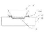
スプリットゲート型メモリセルの製造に関する問題点は、対となるコントロールゲート長及び位置の不一致である可能性がある。図1に示したように、2つのコントロールゲートは、共通ソース領域の一側上に、ソース領域と対応するドレイン領域との間のチャンネル部上へ配置される。もし、コントロールゲート長Lcg1とLcg2とが実質的に同一でなければ、ソースとドレインとの間を流れる電流の量が相異なり、その結果、2つのミラーセルの動作が相異なるようになる。A problem associated with the production of split gate type memory cells may be mismatched control gate length and position mismatch. As shown in FIG. 1, the two control gates are disposed on one side of the common source region and on the channel portion between the source region and the corresponding drain region. If the control gate lengths Lcg1 and Lcg2 are not substantially the same, the amounts of current flowing between the source and the drain are different, and as a result, the operations of the two mirror cells are different.
データは、充電(プログラム)されるか、または放電(削除)される時のフローティングゲート104aの状態についての関数であって、それぞれのトランジスタを通じて流れる電流の変化を利用して、このようなスプリットゲート型メモリセル内に保存されることができる。充電(プログラム)動作の間に、例えば基板をグラウンドである0V近所に維持したままで共通ソースに相対的に高電圧、例えば8〜12Vを、対応するコントロールゲート120に中間電圧、例えば1〜3Vを、そして対応するドレイン126に相対的に低電圧、例えば0〜0.5Vを印加することによって、電子をフローティングゲート104aに注入できる。フローティングゲート104aは、それによるチャンネルホット電子注入(Channel Hot Eletron Injection:CHEI)メカニズムによって電子を蓄積することによって、トランジスタの有効しきい電圧Vthは一般的に約3V以上のレベルまで増加する。The data is a function of the state of the
逆に、放電(削除)動作の間に、例えば、共通ソース116、対応するドレイン126及び基板100をグラウンドである0V、またはその近所に維持させたままでコントロールゲート120に相対的に高電圧、例えば8〜12Vを印加することによってフローティングゲート104aから電子を回収できる。フローティングゲート104aが、それによるF−Nトンネリングメカニズムによってその蓄積された電子を放電させれば、トランジスタの有効しきい電圧であるVthが一般的に約1V未満に減少し、さらには0V未満のレベルまで減少できる。Conversely, during a discharge (deletion) operation, for example, the
一旦、プログラムされるかまたは削除された場合、図1で示したように、コントロールゲート120に約2Vの読み取り電圧を印加し、ドレイン126に約1Vを印加し、ソース116と基板100とをグラウンドである0V、またはその近くに維持することによってスプリットゲートメモリを読み取ることができる。読み取られる時、フローティングゲートが充電されれば、Vthは読み取り電圧を十分に超過してトランジスタが“オフ”となる。逆に、読み取られる時、フローティングゲートが放電されれば、Vthは十分に読み取り電圧未満となってトランジスタが“オン”となることを保証する。周知のように、最終半導体製品についての性能要求を考慮して選択したスプリットゲート型トランジスタ素子の大きさとドーピングとは、このようなトランジスタを動作させるために必要な電圧及び電流の正確な範囲を決定する。Once programmed or deleted, as shown in FIG. 1, a read voltage of approximately 2V is applied to the
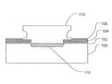
図1に示したように、スプリットゲート型メモリセルは、共通ソース領域116の対向面上にフローティングゲート104a及び対応するコントロールゲート120が配置され、絶縁材料により互いに分離される構造を有する。また、フローティングゲート104aは、外部電流ソースから周囲の絶縁材料によって電気的に孤立される。 As shown in FIG. 1, the split gate type memory cell has a structure in which the
フローティングゲート104aとコントロールゲート120との実質的に垂直な部分の間の絶縁材料200は、ゲート間絶縁層、トンネリング絶縁体またはトンネリング酸化膜と称することができる。フローティングゲート104aと基板100との間の絶縁材料204は、カップリング絶縁体またはカップリング酸化膜と称することができる。類似して、コントロールゲート120と基板100との間の絶縁材料206は、ゲート絶縁体またはゲート酸化膜と称することができる。 The
例えば、絶縁材料204及び206は、製造工程中に他の段階で形成でき、それにより組成及び/または厚さにおいて多少差がありえる。フローティングゲート104aの上部側とコントロールゲート120との間の絶縁材料202は、インターポリ酸化膜(interpoly oxid:IPO)と称することができる。 For example, the
これらの絶縁領域200、202、204、206のそれぞれは、順次にスプリットゲート型トランジスタのための総キャパシタンスCtotに寄与する関連キャパシタンス、即ち、Ctun、CIPO、Cc、Cgを有する。これらのキャパシタンスは、充電(プログラム)動作の間に順次にホット電荷を生成し、それをフローティングゲートに向かわせる電界を生成するように、フローティングゲート104aに印加される電圧に影響を与えることもできる。一般的に、プログラム段階の間に、フローティングゲート104aに誘導された電圧Vfgは、方程式1によって共通ソースに印加された電圧Vsに対応する。Each of these
Vfg=Vs*(Cc/Ctot) … (式1)
したがって、Cc/Ctotの大きさは、スプリットゲート型トランジスタを設計する時に考慮せねばならない因子である。Cc/Ctotがより高い値を有するほどフローティングゲートに誘導される電圧がより高くなり、トランジスタの電子インジェクション(プログラム)効率が増加される。Vfg = Vs * (Cc / Ctot ) (Equation 1)
Therefore, the magnitude of Cc / Ctot is a factor that must be taken into account when designing a split gate transistor. The higher the value of Cc / Ctot , the higher the voltage induced on the floating gate, increasing the transistor's electronic injection (programming) efficiency.
同様に、放電(削除)動作の間に、電子はトンネル絶縁層200及び/またはIPO202を通じたF−Nトンネリングにより、フローティングゲートからコントロールゲートに動く。この場合、一般的に、フローティングゲート104aに誘導された電圧Vfgは、次式2によってコントロールゲートに印加された電圧Vcgに対応する。Similarly, during the discharge (deletion) operation, electrons move from the floating gate to the control gate by FN tunneling through the
Vfg=Vcg*((Ctot−CIPO−Cg)/Ctot) … 式2
したがって、向上した性能のために、CIPOを増加させてフローティングゲート上の有効電圧Vfgを減少させることが望ましい。放電動作の間のVfgの減少は、電子放電(削除)効率だけでなくメモリセルの耐久性に影響を及ぼす。さらに、F−Nトンネリングメカニズムを利用する場合に、トンネル電流は絶縁層内の電子トラップにより減少されるので、装置の性能を劣化させる。この劣化は、フローティングゲートの有効電圧を増加させることによって多少抑制できる。Vfg = Vcg * ((Ctot −CIPO −Cg ) / Ctot ) Equation 2
Therefore, in order to improve performance, it is desirable to reduce the effective voltage Vfg of the floating gate by increasing the CIPO. The decrease in Vfg during the discharge operation affects not only the electron discharge (deletion) efficiency but also the durability of the memory cell. Furthermore, when utilizing the FN tunneling mechanism, the tunnel current is reduced by electron traps in the insulating layer, thus degrading the performance of the device. This deterioration can be somewhat suppressed by increasing the effective voltage of the floating gate.
また、トンネリングとIPOとが有するフローティングゲートの挙動についてのキャパシタンスの寄与分Ctun及びCIPO間の関係は、次式3によってカップリング比率αで表現できる。Also, the relationship between the capacitance contribution Ctun and CIPO regarding the behavior of the floating gate of the tunneling and the IPO can be expressed by the coupling ratio α by the following equation (3).
α=((Ctun+CIPO)/Ctot) … (式3)
特許文献1ないし8には、所定の製造工程と、それによるフローティングゲート構造とが示されて説明されており、参照としてその全文がこれに含まれている。α = ((Ctun + CIPO ) / Ctot ) (Equation 3)
Patent Documents 1 to 8 show and explain a predetermined manufacturing process and a floating gate structure by the predetermined manufacturing process, and the entire text thereof is included as a reference.
本発明は、上記事情に鑑みてなされてものであり、自己整列されたフローティングゲートとコントロールゲート構造とを有する不揮発性スプリットゲート型メモリセルと、かかるメモリセルについて、このスプリットゲート素子の相対的長さと分離についてより向上した大きさ制御を可能にする製造工程を提供する。 The present invention has been made in view of the above circumstances, and a non-volatile split gate type memory cell having a self-aligned floating gate and a control gate structure, and the relative length of the split gate element for such a memory cell. A manufacturing process is provided that allows for more improved size control for sag and separation.
本発明によるスプリットゲート型トランジスタの実施例は、コントロールゲート及びフローティングゲートの自己整列を提供し、トンネリング及びIPOについての制御を向上させる。これらの工程及び構造的向上は、向上したプログラム/削除効率、耐久性及び装置間の均一性といえる。 Embodiments of the split-gate transistor according to the present invention provide control gate and floating gate self-alignment to improve control over tunneling and IPO. These process and structural improvements can be referred to as improved program / delete efficiency, durability, and uniformity between devices.
本発明によるスプリットゲート型トランジスタを形成する実施例は、基板上に第1絶縁層を形成する段階、第1絶縁層上に第1半導体層を形成する段階、第1半導体層上に第2絶縁層を形成する段階、第2絶縁層上に第3絶縁層を形成する段階、第3絶縁層をパターニング及びエッチングして実質的に垂直な側壁を有し、第2絶縁層の一部を露出させる開口を形成する段階、第1半導体層の一部を酸化させて半導体酸化物層を形成する段階、第2半導体層を蒸着する段階、非等方エッチングを利用して前記第2半導体層をエッチングして、開口の側壁に隣接するスペーサを形成し、半導体酸化物層の一部を露出させる段階、半導体酸化物層の露出された一部をエッチングして、第1絶縁層の一部を露出させる段階、第4絶縁層を、開口を充填するのに十分の厚さで蒸着する段階、第4絶縁層の上部を除去して第3絶縁層の表面を露出させ、実質的に平坦な表面を形成する段階、スペーサを実質的に維持しつつ、第3絶縁層を除去してベース構造を形成する段階、ベース構造をエッチングマスクとして使用して、第1半導体層をエッチングして第1絶縁層を露出させ、フローティングゲート構造を形成する段階、フローティングゲート構造上に絶縁層を形成する段階、ベース構造の表面に実質的に順応する第3半導体層を蒸着する段階、第3半導体層をエッチングして、それぞれが対を成すが該当フローティングゲート構造から絶縁され、それぞれの一部が少なくとも部分的に該当フローティングゲート構造の上部に配置されるように、ベース構造の側壁に隣接するコントロールゲート構造を形成する段階、第4絶縁層を蒸着してコントロールゲート構造を絶縁する段階を順次に含む。 An embodiment of forming a split-gate transistor according to the present invention includes a step of forming a first insulating layer on a substrate, a step of forming a first semiconductor layer on the first insulating layer, and a second insulating layer on the first semiconductor layer. Forming a layer, forming a third insulating layer on the second insulating layer, patterning and etching the third insulating layer to have substantially vertical sidewalls, exposing a portion of the second insulating layer Forming an opening to be formed, oxidizing a part of the first semiconductor layer to form a semiconductor oxide layer, depositing a second semiconductor layer, and anisotropic etching to form the second semiconductor layer. Etching to form a spacer adjacent to the sidewall of the opening, exposing a portion of the semiconductor oxide layer, etching the exposed portion of the semiconductor oxide layer, and removing a portion of the first insulating layer Exposing, filling the opening with the fourth insulating layer Depositing a sufficient thickness to remove the upper portion of the fourth insulating layer to expose the surface of the third insulating layer to form a substantially flat surface; substantially maintaining the spacer; Meanwhile, removing the third insulating layer to form a base structure, using the base structure as an etching mask, etching the first semiconductor layer to expose the first insulating layer, and forming a floating gate structure Forming an insulating layer on the floating gate structure; depositing a third semiconductor layer substantially conforming to a surface of the base structure; and etching the third semiconductor layer to form a pair, but the corresponding floating gate Control gates adjacent to the side walls of the base structure so that they are isolated from the structure and each part is at least partially located on top of the corresponding floating gate structure. Forming a structure sequentially including the step of isolating the control gate structure by depositing a fourth insulating layer.
また、不揮発性スプリットゲート型メモリセルを製造する実施例を開示しており、この実施例は、基板上に第1絶縁層を形成する段階、第1絶縁層上に第1半導体層を形成する段階、第1半導体層上に第2絶縁層を形成する段階、第2絶縁層上に第3絶縁層を形成する段階、第3絶縁層をパターニング及びエッチングして、実質的に垂直な側壁を有し、第2絶縁層の一部を露出させる開口を形成する段階、第1半導体層の一部を酸化させて半導体酸化物層を形成する段階、側壁材料層を蒸着する段階、非等方エッチングを利用して側壁材料層をエッチングして、開口の側壁に隣接するスペーサを形成し、半導体酸化物層の一部を露出させる段階、半導体酸化物層の露出された部分をエッチングして、第1半導体層の一部を露出させる段階、第1半導体層の露出された部分をエッチングして、第1絶縁層の一部を露出させる段階、第1絶縁層の露出された部分を通じてドーパント種を注入して、基板の一部にソース領域を形成する段階、開口を充填するのに十分の厚さで第4絶縁層を蒸着する段階、第4絶縁層の上部を除去して、第3絶縁層の表面を露出させて実質的に平坦な表面を形成する段階、第3絶縁層及びスペーサを除去して、凹領域を含む側壁を有する絶縁体構造を形成する段階、第2絶縁層を除去する段階、半導体酸化物層の残存部を利用して第1半導体層をエッチングして、第1絶縁層を露出させて第1導電体要素を形成する段階、第1導電体要素上に第5絶縁層を形成する段階、絶縁体構造の表面に実質的に順応し、側壁の凹領域を充填する第2半導体層を蒸着する段階、第2半導体層をエッチングして、それぞれが対を成してその一部が該当第1導電体要素の上部に配置される半導体スペーサを絶縁体構造の側壁に隣接するように形成し、第1絶縁層の一部を露出させる段階、第1絶縁層の露出部を通じてドーパント種を注入して、基板内にドレイン領域を形成する段階、第2導電体要素を絶縁させる絶縁層を形成し、ソース領域、ドレイン領域、及び前記第2導電体要素に独立された電気的接続を提供する段階を順次に含む。 Further, an embodiment for manufacturing a nonvolatile split gate type memory cell is disclosed. In this embodiment, a first insulating layer is formed on a substrate, and a first semiconductor layer is formed on the first insulating layer. Forming a second insulating layer on the first semiconductor layer; forming a third insulating layer on the second insulating layer; patterning and etching the third insulating layer to form substantially vertical sidewalls; Forming an opening exposing a portion of the second insulating layer, oxidizing a portion of the first semiconductor layer to form a semiconductor oxide layer, depositing a sidewall material layer, anisotropic Etching the sidewall material layer to form a spacer adjacent to the sidewall of the opening, exposing a portion of the semiconductor oxide layer, etching the exposed portion of the semiconductor oxide layer; Exposing a portion of the first semiconductor layer; Etching the exposed portion of the semiconductor layer to expose a portion of the first insulating layer; implanting dopant species through the exposed portion of the first insulating layer to form a source region in a portion of the substrate; Performing a step of depositing a fourth insulating layer with a thickness sufficient to fill the opening; removing a top portion of the fourth insulating layer to expose a surface of the third insulating layer; Forming the insulator structure having sidewalls including the recessed regions by removing the third insulating layer and the spacer, removing the second insulating layer, and utilizing the remaining portion of the semiconductor oxide layer. Etching the first semiconductor layer to expose the first insulating layer to form a first conductor element; forming a fifth insulating layer on the first conductor element; and Depositing a second semiconductor layer that substantially conforms and fills the recessed region of the sidewall. Etching the second semiconductor layer to form a semiconductor spacer adjacent to the side wall of the insulator structure, each of which forms a pair and a part of which is disposed on top of the corresponding first conductor element; Exposing a portion of the first insulating layer; implanting dopant species through an exposed portion of the first insulating layer to form a drain region in the substrate; and forming an insulating layer for insulating the second conductor element. Sequentially providing independent electrical connections to the source region, the drain region, and the second conductor element.
また、実施例えば補償フローティングゲート及びコントロールゲートを形成する方法を開示しており、本方法は、凹領域及び凸領域を有する側壁表面を備え、この凸領域が凹領域の下部に配置される絶縁体構造を形成する段階、エッチマスクとして絶縁体構造の凸領域を利用して、半導体層をエッチングしてフローティングゲート構造を形成する段階、フローティングゲート上に絶縁層を形成して、凹領域を含む側面を有する中間絶縁体構造を形成する段階、及び側面に順応し、フローティングゲート構造の一部上に延長された凸部を含むコントロールゲート構造を中間絶縁体構造に隣接して形成する段階を含む。 Also disclosed is a method of forming, for example, a compensation floating gate and a control gate, the method comprising a sidewall surface having a concave region and a convex region, wherein the convex region is disposed below the concave region. Forming a structure; using a convex region of an insulator structure as an etch mask; etching a semiconductor layer to form a floating gate structure; forming an insulating layer on the floating gate to form a side surface including a concave region; And forming a control gate structure adjacent to the intermediate insulator structure that includes a protrusion adapted to the side surface and extending on a portion of the floating gate structure.
本発明による製造工程の実施例は、第1ポリシリコンスペーサ114a、フローティングゲート104a上の絶縁層、及びコントロールゲート構造120の形成を制御することによって、コントロールゲートとフローティングゲートとの間に配置された絶縁材料だけでなく、フローティングゲート104aとコントロールゲート120との相対的な大きさ及び位置についての制御をより向上させる。この向上した制御は、自己整列構造と結合して、より一貫された性能と向上した効率とを有するスプリットゲート型メモリ装置を形成する方法を提供する。さらに、ゲート構造の相対的な大きさについての向上した制御は、プログラム/削除効率の増加と向上した耐久性とを有する装置の生産を可能にする。 An embodiment of the manufacturing process according to the present invention is disposed between the control gate and the floating gate by controlling the formation of the
以下、本発明によるスプリットゲート型トランジスタ構造、及びこのようなスプリットゲート型トランジスタ構造の製造方法についての実施例を、添付された図面を参照してさらに詳細に説明する。しかし、周知のように、本発明は複数の他の形態で実施でき、以下に開示された実施例に限定されるものと解釈されてはならず、かえって、これらの実施例は本開示を完全にするために提供されたものであり、当業者に本発明の思想を完全に伝達する。 Hereinafter, embodiments of a split gate transistor structure according to the present invention and a method of manufacturing such a split gate transistor structure will be described in more detail with reference to the accompanying drawings. However, as is well known, the present invention may be implemented in a number of other forms and should not be construed as limited to the embodiments disclosed below, but rather, these embodiments fully To fully convey the spirit of the present invention to those skilled in the art.
図面は、以下でさらに詳細に説明しようとする本発明の実施例の理解を助けるためのものであり、不当に本発明を制限するものと解釈されてはならない。特に、図面に示された多様な素子の相対的間隔、大きさ及び寸法は、実際のスケールではなく、より明確な説明のために、誇張、減縮されるか、または変形されることもある。また、当業者は、例えばフォトレジストパターン及び多層金属配線構造を含む半導体装置の製造時に一般的に使われる所定の層を省略して単純化し、明確性を向上させ、図面の数を減少させたということが分かる。 The drawings are intended to assist in understanding embodiments of the invention that will be described in further detail below, and should not be construed to unduly limit the invention. In particular, the relative spacing, size, and dimensions of the various elements shown in the drawings are not actual scales, and may be exaggerated, reduced, or modified for a clearer description. In addition, those skilled in the art have simplified by omitting predetermined layers generally used in manufacturing a semiconductor device including, for example, a photoresist pattern and a multilayer metal wiring structure, improving clarity, and reducing the number of drawings. I understand that.
以下で使われたように、他の層または基板“上に”または“上へ”と説明された層または構造は、参照された層または基板に直接的に形成されるか、または積層される必要はなく、一つ以上の中間層を含むと理解せねばならない。類似して、層または構造が他の層または表面の“下部に”あると説明する場合には、層または構造が必ずしも参照された層または表面の下部に直接的に配置されるものではなく、一つ以上の中間層を含むことができると理解せねばならない。したがって、“隣接した”及び“傍の”という用語も、相対的な方向を説明するものと理解せねばならず、中間層または材料を含んでいると理解せねばならない。 As used below, a layer or structure described as “on” or “up” to another layer or substrate is directly formed or stacked on the referenced layer or substrate. It is not necessary and must be understood to include one or more intermediate layers. Similarly, if a layer or structure is described as “underneath” another layer or surface, the layer or structure is not necessarily placed directly below the referenced layer or surface; It should be understood that one or more intermediate layers can be included. Thus, the terms “adjacent” and “neighboring” should also be understood to describe relative directions and should be understood to include intermediate layers or materials.
図2A〜図2Mは、本発明による工程の実施例を示す。図2Aに示したように、例えばP型シリコンである半導体基板100を備え、例えばその上にシリコン酸化物として、一般的に約50〜150Åの厚さを有する第1絶縁層102を基板の酸化または蒸着工程により形成する。半導体基板100とは、たとえば、半導体ウエハであり、p型半導体ウエハである。次に、第1ポリシリコン層(第1半導体層)104は、一般的に500〜1500Åの厚さを有し、第1絶縁層上に形成される。意図的に、第1ポリシリコン層104は、フローティングポリまたはFポリとも称することができる。次に、第2絶縁層106は、一般的に約30〜100Åの厚さを有する薄いシリコン酸化物層であり、例えば、第1ポリシリコン層の一部を酸化させることによって、第1ポリシリコン層104上に形成する。 2A-2M show an example of a process according to the present invention. As shown in FIG. 2A, a
第3絶縁層108は、例えば、約2000〜3000Åの厚さを有するシリコン窒化物層であり、一般的に低圧CVD(LPCVD)、プラズマ強化CVD(Plasma Enhanced CVD:PECVD)のような化学気象蒸着(CVD)や、他の適切な蒸着工程を利用して第2絶縁層106上に形成する。次に、第3絶縁層108上にフォトレジスト層(図示せず)を形成し、露光及び現像して第3絶縁層の一部を露出させるフォトレジストパターンを形成する。次に、第3絶縁層108の露出部をエッチングして、第2絶縁層106の一部を露出させる開口またはトレンチ110を形成する。例えば、望ましくは、利用されたエッチング工程は、例えば第2絶縁層106についての第3絶縁層108に対して10以上の比較的高選択比を有する。 The third
図2Bに示したように、第2絶縁層106の露出部と、さらに詳細にはポリシリコン層104の下部とは、追加的な酸化工程を経て、トレンチ110内に露出された第3絶縁層108のエッジの下部に延長され、減少された厚さを有する一定の鳥のくちばし(bird’s beak)状の領域を含むFポリ酸化物領域112(半導体酸化物層)を含む。一般的にFポリ酸化物112は、約500〜1500Åの厚さを有し、酸化する間にFポリ厚さの半分以上を消耗できる。なお、第1ポリシリコン層104の厚さは、該第1ポリシリコン層104上の露出された部分上に形成されたFポリ酸化物領域112の厚さの少なくとも約90%以上、約110%未満である。また、Fポリ酸化物領域112の下部にある第1ポリシリコン層104の厚さは、蒸着された状態の他の第1ポリシリコン層104の厚さの少なくとも40%以上である。 次に、図2Cに示したように、第3絶縁層108及びFポリ酸化物112上に、一般的に順応する第2ポリシリコン層114(第2半導体層、側壁材料層)を蒸着する。第2ポリシリコン層114は、一般的に約1500〜3000Åの厚さを有する。 As shown in FIG. 2B, the exposed portion of the second insulating
次に、図2Dに示したように、この第2ポリシリコン層114は、反応性イオンエッチング(RIE)のような非等方性エッチング工程を経て、トレンチ110の側面に隣接するポリシリコンスペーサ114aを形成する。ポリシリコンスペーサ114aは、一般的に約0.15〜0.25μmの底部幅wで特性分析を行え、Fポリ酸化物112の周辺部を被覆する。トレンチ110の中央部内に形成されたポリシリコン層114の部分は、スペーサ形成中に除去され、Fポリ酸化物112の一部を露出させる。 Next, as shown in FIG. 2D, the
次に、図2Eに示したように、Fポリ酸化物112の露出部を除去して、Fポリ酸化物112がスペーサ114aの下部に残存するようにFポリ104の一部を露出させる。 Next, as shown in FIG. 2E, the exposed portion of the
次に、図2Fに示したように、Fポリ104の露出部を除去して、第1絶縁層102の一部を除去できる。また、Fポリ104の露出部を除去するために利用されるエッチング工程は、トレンチ110の側壁に隣接する減少されたポリシリコンスペーサ114bを形成する特徴がある。露出されたポリシリコン領域104、114a及び第1絶縁層102についてのエッチング選択度と、第1絶縁層の相対的な厚さとは、このエッチング工程でポリシリコンスペーサ114aがどの程度除去されるか、そして底部幅wがどの程度減少するかを決定する。最終底部幅wは、0.1μm台である可能性がある。 Next, as shown in FIG. 2F, a portion of the first insulating
図2Fに示したように、一旦Fポリの露出部が除去されれば、約40KeVのエネルギで約1015イオン/cm2の次数を有するドーズで、n型ドーパント、例えばAsまたはPのようなドーパント種を基板に注入させて、トランジスタ用共通ソース領域116を形成する。As shown in FIG. 2F, once the exposed portion of F-poly is removed, at a dose having an order of about 1015 ions / cm2 at an energy of about 40 KeV, an n-type dopant such as As or P Dopant species are implanted into the substrate to form a
次に、図2Gに示したように、ソース注入を完成した後には、基板上に厚いシリコン酸化物層(図示せず:第4絶縁層)を蒸着する。このシリコン酸化物層は、トレンチ110を完全に充填できるように十分な厚さを有せねばならず、15,000Å程度に厚い可能性がある。次に、一般的に化学的機械的研磨(CMP)工程を利用してこのシリコン酸化物層の上部を除去して、第3絶縁層108の上部表面を露出させて実質的に平坦な表面を形成する。シリコン酸化物の残存部は、トレンチ110を完全に充填させる孤立された酸化物構造118(第4絶縁層)を形成する。 Next, as shown in FIG. 2G, after completing the source implantation, a thick silicon oxide layer (not shown: fourth insulating layer) is deposited on the substrate. This silicon oxide layer must be thick enough to completely fill the
図2Hに示したように、酸化物構造118を形成した後に、第3絶縁層108を除去する。第3絶縁層108がシリコン窒化物である実施例において、一般的に150℃以上の熱い燐酸(H3PO3)水溶液を含む湿式エッチング工程を利用して除去できる。一旦、第3絶縁層108が除去されれば、減少されたポリシリコンスペーサ114bは露出されて、水酸化アンモニウム(NH4OH)の水溶液を含む湿式エッチング工程を利用して除去できる。これによる構造(ベース構造)の露出部は、酸化物構造118及び第2絶縁層106の残存部を含む。As shown in FIG. 2H, after the
次に、図2Iに示したように、一般的にFポリ層104の一部を露出させるように、湿式エッチングまたは乾式エッチングを利用して第2絶縁層106の残存部を除去する。エッチング組成によって、減少されたポリシリコンスペーサ114bの除去と関連して第2絶縁層106の残存部を除去できる。第2絶縁層106の残存部を除去した後に、エッチングマスクとして酸化物構造118を利用して、Fポリ層104の露出部をエッチングして第1絶縁層102を露出させる。Fポリ層104の残存部は、フローティングゲート構造104a(第1導電体要素)となる。 Next, as shown in FIG. 2I, the remaining portion of the second insulating
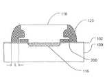
次に、図2Jに示したように、熱酸化及び/またはCVD工程を通じて酸化物構造118の露出表面とフローティングゲート構造104a上に、一般的に約50〜150Åの厚さを有する絶縁酸化物層(第5絶縁層)を形成してフローティングゲート構造を絶縁させ、ゲート酸化膜を形成する。次に、基板上に約2000〜4000Åの厚さで第3ポリシリコン層(図示せず:第3半導体層)を蒸着し、RIEのような非等方性エッチバック工程を経て、酸化物構造118に隣接するコントロールゲート構造120(第2導電体要素)を形成する。また、ワードラインポリシリコンとも称するコントロールゲート構造120は、トンネリング酸化物200から延長して、基板100のチャンネル領域に渡って底部長Lと特徴付けることができる。この底部長Lは、蒸着されたポリシリコン層の厚さ、エッチング化学及び過剰エッチング程度により調節され、寸法制御を可能にする。一般的な底部長Lは、約0.20〜0.35μmの範囲である。 Next, as shown in FIG. 2J, an insulating oxide layer generally having a thickness of about 50 to 150 mm on the exposed surface of the
図2Kに示したように、基板100内に注入マスクとして酸化物構造118とコントロールゲート構造120とを使用して、若干ドーピングされた低濃度ドレイン(LDD)領域122を形成できる。共通ソース領域のように、LDD領域122(第1ドーズ)は、一般的にN−ドレイン領域を形成する約1013イオン/cm2の減少されたドーズ、約40KeVのエネルギでAs及び/またはPである一つ以上のn型ドーパント(第1ドーパント種)を注入して形成できる。As shown in FIG. 2K, a lightly doped lightly doped drain (LDD)
LDD領域122を形成した後には、図2Lに示したように、基板上に酸化物層(図示せず)を蒸着して、RIEのような非等方性エッチバック工程を経て、コントロールゲート120の側面に隣接する酸化物スペーサ(第6絶縁層)124を形成する。注入マスクとして酸化物構造118、コントロールゲート構造120、及び酸化物スペーサ124を利用して、基板に一般的にAsまたはPであるn型ドーパント(第2ドーパント種)の追加的な過剰注入を行ってN+ドレイン領域126(第2ドーズ)を形成でき、一般的に共通ソース領域を形成するために使用する注入エネルギとドーズとの組み合わせに相応する組み合わせを利用する。このような高濃度のドレイン領域は、N+ビットラインジャンクションとも称する。LDD領域122へのドーパントの注入量は、N+ドレイン領域126へのドーパントの注入量に対して、1/25以下である。 After forming the
図2Mに示したように、N+ドレイン領域126の形成後に、基板上に一般的に約10,000〜15,000Åの厚さを有するCVD酸化物である厚い酸化物層128を形成する。この酸化物層128は、CMP工程を利用して平坦化させて、パターニングにさらに適した表面を提供する。次に、酸化物層128上にフォトレジスト層(図示せず)を形成し、露光及び現像して、酸化物層の一部を露出させる接続パターンを形成する。次に、酸化物層128の露出部をエッチングして、ソース領域116、ドレイン領域126(図示せず)及びコントロールゲート120(図示せず)に延長される接続開口を形成する。フォトレジストパターンを除去した後に、一般的にTi及びTiNの組み合わせを含む初期バリヤー金属を含む一つ以上の導電性材料で接続開口を充填し、Wのような他の金属層を蒸着して残りの接続開口を充填した後、CMP工程により金属側の上部を除去して下地素子に電気的接続を提供する接続プラグ130を形成する。例えば、タングステンを利用した工程は、約2000〜3000Åの厚さを有するW層の蒸着を含み、次に、タングステンCMP工程を行って厚い酸化物128の上部表面を露出させ、接続開口部内にWプラグを形成する。 As shown in FIG. 2M, after forming the N +
以上のようにして、スプリットゲート型トランジスタが形成される。ここで、フローティングゲート104aは、断面積Afを有し、コントロールゲート120は、断面積Ac及び凸部を有する。凸部は、ソース領域116方向にフローティングゲートの外部上に延長され、Af対Acの比は、約1:2〜1:10である。As described above, a split gate transistor is formed. Here, the floating
フローティングゲート104aは、ゲート長Lfを有し、コントロールゲート120の凸部は、フローティングゲート104a上に距離Lpほど延長され、LpとLfとの比は、約2:3〜1:5である。Floating
また、コントロールゲート120の凸部の下部の底面は、厚さTIPOを有するインターポリ酸化物によりフローティングゲート104a電極から分離されている。また、コントロールゲート120の凸部以外の部分(非凸部)の下部は、厚さTtunを有するトンネリング酸化物によりフローティングゲート104aから分離された実質的に垂直な表面を含む。コントロールゲート120の非凸部の下部は、誘電体層からなるゲート酸化物部分によってLDD122から分離された実質的に水平な表面を含み、前記ゲート酸化物はTgの厚さを有する。フローティングゲート104aの下部は、誘電体層からなる厚さTcのカップリング酸化物部分により前記チャンネル領域から分離された実質的に垂直な表面を含む。このスプリットゲート型セル構造において、TIPO>Ttun、TIPO>Tc及びTIPO>Tgの関係が満足される。Also, the bottom surface of the lower portion of the convex portion of the
TcとTgとの比は、約3:1〜1:3であることが好ましい。さらに好ましくは、TcとTgとの比は、約1:1である。The ratio between Tc and TheT g of about 3: 1 to 1: 3. More preferably, the ratio of Tc to Tg is about 1: 1.
導電性材料で接続開口を充填した後に、基板上に、例えばアルミニウムまたはアルミニウム合金の他の金属層を形成する。次に、金属配線層132を形成するために、この金属層をパターニングしてエッチングする。周知のように、必要であるか、または望ましい場合、層間絶縁体(図示せず)を蒸着し、金属配線からなる第1層132へのバイアスを開口させ、導電性ビアプラグ(図示せず)及び金属配線(図示せず)からなる第2層を形成することによって、追加的な金属配線層(図示せず)を形成できる。 After filling the connection openings with a conductive material, another metal layer of, for example, aluminum or an aluminum alloy is formed on the substrate. Next, in order to form the
実施例を参照して本発明を説明したが、本発明はこれに限定されず、当業者が特許請求の範囲で定義された本発明の思想と範囲とを逸脱せずに、特に、多様な層の組成と相対的厚さに関連した多様な変形形態の存在を認識できるということは自明である。 Although the present invention has been described with reference to examples, the present invention is not limited thereto, and various modifications can be made by those skilled in the art without departing from the spirit and scope of the invention as defined in the claims. It is self-evident that the existence of various deformations related to the composition and relative thickness of the layer can be recognized.
本発明は、コントロールゲートが共通ソース領域に対して対称なミラー対を有するスープレットゲート型メモリセル構造で、コントロールゲートの相対的な大きさ及び位置についての正確な制御に使われることができる。 The present invention is a supelet gate type memory cell structure in which the control gate has a mirror pair symmetrical with respect to a common source region, and can be used for precise control of the relative size and position of the control gate.
100 基板、
104a フローティングゲート、
116 ソース領域、
120 コントロールゲート、
122 LDD領域、
126 ドレイン、
128 酸化物層、
132 金属配線層、
200、202、204、206 絶縁材料。100 substrates,
104a floating gate,
116 source region,
120 control gate,
122 LDD region,
126 drain,
128 oxide layer,
132 metal wiring layer,
200, 202, 204, 206 Insulating material.
Claims (35)
Translated fromJapaneseb)前記絶縁構造の凸領域をエッチングマスクとして利用して、半導体層をエッチングしてフローティングゲート構造を形成する段階と、
c)前記フローティングゲート構造上に絶縁層を形成して、前記フローティングゲート構造を統合し、凹領域を含む側面を有する中間絶縁構造を形成する段階と、
d)前記中間絶縁構造に隣接し、前記側面に順応しつつ、前記フローティングゲート構造の一部上に延長される突出領域を含むコントロールゲート構造を形成する段階と、を順次に含むことを特徴とするスプリットゲート型トランジスタの製造方法。a) forming an insulating structure having a concave region and a side wall with a convex region disposed below the concave region;
b) using the convex region of the insulating structure as an etching mask to etch the semiconductor layer to form a floating gate structure;
c) forming an insulating layer on the floating gate structure, integrating the floating gate structure, and forming an intermediate insulating structure having a side surface including a concave region;
and d) sequentially forming a control gate structure including a protruding region that is adjacent to the intermediate insulating structure and is adapted to the side surface and extends on a part of the floating gate structure. A method for manufacturing a split gate transistor.
前記コントロールゲート構造を形成した後に、前記基板内にドレイン領域を形成する段階と、
前記ドレイン領域を形成した後に、厚い絶縁層を形成する段階と、
前記厚い絶縁層を通じて複数の接続開口を形成して、電気的接続が前記共通ソース、前記ドレイン及び前記コントロールゲート構造に独立的に行われる段階と、をさらに含むことを特徴とする請求項1に記載のスプリットゲート型トランジスタの製造方法。Forming a common source region in the substrate before forming the insulating structure;
Forming a drain region in the substrate after forming the control gate structure;
Forming a thick insulating layer after forming the drain region;
The method of claim 1, further comprising: forming a plurality of connection openings through the thick insulating layer, wherein electrical connection is made independently to the common source, the drain and the control gate structure. A manufacturing method of the split gate type transistor described.
前記接続開口内のTi層上にTiN層を蒸着する段階と、
前記接続開口内のTiN層上にW層を蒸着する段階と、
前記基板を平坦化して前記厚い絶縁層の表面を露出させて、前記接続開口を充填するタングステンプラグを形成する段階と、をさらに含むことを特徴とする請求項2に記載のスプリットゲート型トランジスタの製造方法。Depositing a Ti layer in the connection opening;
Depositing a TiN layer on the Ti layer in the connection opening;
Depositing a W layer on the TiN layer in the connection opening;
3. The split gate transistor according to claim 2, further comprising: planarizing the substrate to expose a surface of the thick insulating layer to form a tungsten plug filling the connection opening. Production method.
窒化物層内に形成されたトレンチに、トレンチ壁に隣接して形成されるように犠牲ポリシリコンスペーサを形成する段階と、
シリコン酸化物で前記トレンチの残余部を充填し、前記シリコン酸化物を平坦化して前記窒化物層の上部表面を露出させる段階と、
前記窒化物層を除去する段階と、
前記ポリシリコンスペーサを除去して前記絶縁構造を形成する段階と、をさらに含むことを特徴とする請求項2に記載のスプリットゲート型トランジスタの製造方法。Forming the concave region comprises:
Forming a sacrificial polysilicon spacer in a trench formed in the nitride layer to be formed adjacent to the trench wall;
Filling the remainder of the trench with silicon oxide and planarizing the silicon oxide to expose an upper surface of the nitride layer;
Removing the nitride layer;
The method of claim 2, further comprising: removing the polysilicon spacer to form the insulating structure.
窒化物層にトレンチを形成する段階と、
前記窒化物層の下部に形成されたポリシリコン層の一部を酸化させて、前記窒化物層の周辺部の下に延長されるシリコン酸化物層を形成する段階と、
前記トレンチの残余部をシリコン酸化物で充填し、前記シリコン酸化物を平坦化して前記窒化物層の上部表面を露出させる段階と、
前記窒化物層を除去する段階と、
前記窒化物層の下部に形成されたシリコン酸化物パッド層を除去する段階と、を含むことを特徴とする請求項2に記載のスプリットゲート型トランジスタの製造方法。Forming the convex region comprises:
Forming a trench in the nitride layer;
Oxidizing a portion of the polysilicon layer formed under the nitride layer to form a silicon oxide layer extending under the periphery of the nitride layer;
Filling the remainder of the trench with silicon oxide, planarizing the silicon oxide to expose an upper surface of the nitride layer;
Removing the nitride layer;
The method according to claim 2, further comprising: removing a silicon oxide pad layer formed under the nitride layer.
テーパ状の薄い末端部を含み、
前記フローティングゲート構造の上部表面は前記凸領域の下部表面に順応し、前記薄い末端部は対応してフローティングゲートの厚さを増加させ、前記フローティングゲート構造上に上向きの突出領域を形成することを特徴とする請求項5に記載のスプリットゲート型トランジスタの製造方法。Forming the convex region comprises:
Including a tapered thin end,
The upper surface of the floating gate structure is adapted to the lower surface of the convex region, and the thin end portion correspondingly increases the thickness of the floating gate to form an upward protruding region on the floating gate structure. 6. The method of manufacturing a split gate transistor according to claim 5, wherein:
b)前記側壁に隣接する第1ポリシリコンスペーサを形成する段階と、
c)前記絶縁層の露出部及び前記絶縁層の下部に形成された半導体層の一部を除去することによって、第1ポリシリコンスペーサの一部を除去して減少されたポリシリコンスペーサを形成し、拡張されたトレンチを形成する段階と、
d)前記拡張されたトレンチをシリコン酸化物で充電する段階と、
e)前記マスクパターン及び前記減少されたポリシリコンスペーサを除去して、凹領域とその凹領域の下部に配置された凸領域とをそれぞれ含む側壁を有する酸化物構造を形成する段階と、
f)前記酸化物構造をエッチングマスクで使用して半導体層の一部を除去することによって、前記凸領域の下部に配置されたフローティングゲート構造を形成する段階と、
g)前記フローティングゲートを取り囲む絶縁構造を形成する段階と、
h)前記凹領域に延長して、該当フローティングゲート構造上に少なくとも一部分が延長されるコントロールゲート構造を、前記酸化物構造の側壁に隣接して形成する段階と、を順次に含むことを特徴とするスプリットゲート型トランジスタの製造方法。a) forming a mask pattern on the substrate having a substantially vertical sidewall and including a trench exposing a portion of the insulating layer formed on the semiconductor layer;
b) forming a first polysilicon spacer adjacent to the sidewall;
c) forming a reduced polysilicon spacer by removing a part of the first polysilicon spacer by removing an exposed portion of the insulating layer and a part of the semiconductor layer formed under the insulating layer; Forming an extended trench; and
d) charging the extended trench with silicon oxide;
e) removing the mask pattern and the reduced polysilicon spacer to form an oxide structure having sidewalls each including a concave region and a convex region disposed under the concave region;
f) forming a floating gate structure disposed under the convex region by removing a portion of the semiconductor layer using the oxide structure as an etching mask;
g) forming an insulating structure surrounding the floating gate;
and h) sequentially forming a control gate structure extending at least partially on the corresponding floating gate structure and extending adjacent to the sidewall of the oxide structure. A method for manufacturing a split gate transistor.
前記第3絶縁層がパターニングされ、エッチングされてマスクパターンを形成し、
半導体酸化物層が形成されるように、前記第1半導体層の一部を酸化させて前記絶縁層が形成され、
ポリシリコン層を蒸着し、非等方エッチングを利用してポリシリコン層をエッチングし、前記第1ポリシリコンスペーサが形成されることを特徴とする請求項7に記載のスプリットゲート型トランジスタの製造方法。The substrate includes a first insulating layer formed on the substrate, a first semiconductor layer formed on the first insulating layer, a second insulating layer formed on the first semiconductor layer, and the second insulating layer. A third insulating layer formed on the layer;
The third insulating layer is patterned and etched to form a mask pattern;
The insulating layer is formed by oxidizing a part of the first semiconductor layer so that a semiconductor oxide layer is formed,
8. The method of manufacturing a split gate transistor according to claim 7, wherein the first polysilicon spacer is formed by depositing a polysilicon layer and etching the polysilicon layer using anisotropic etching. .
前記第2半導体層を非等方エッチングして、前記酸化物構造の側壁に隣接する半導体スペーサを形成する段階と、を含むことを特徴とする請求項8に記載のスプリットゲート型トランジスタの製造方法。Depositing the second semiconductor layer substantially conforming to the surface of the oxide structure and filling the recessed region to form the control gate structure;
9. The method of manufacturing a split gate transistor according to claim 8, further comprising: anisotropically etching the second semiconductor layer to form a semiconductor spacer adjacent to a sidewall of the oxide structure. .
b)前記第1絶縁層上に第1半導体層を形成する段階と、
c)前記第1半導体層上に第2絶縁層を形成する段階と、
d)前記第2絶縁層上に第3絶縁層を形成する段階と、
e)前記第3絶縁層をパターニングしてエッチングして、実質的に垂直な側壁を有し、前記第2絶縁層の一部を露出させる開口を形成する段階と、
f)前記第1半導体層の一部を酸化させて半導体酸化物層を形成する段階と、
g)第2半導体層を蒸着する段階と、
h)非等方エッチングを利用して前記第2半導体層をエッチングして、前記開口の側壁に隣接するスペーサを形成し、前記半導体酸化物層の一部を露出させる段階と、
i)前記半導体酸化物層の露出された一部をエッチングして、前記第1半導体層の一部を露出させる段階と、
j)前記第1半導体層の露出された一部をエッチングして、前記第1絶縁層の一部を露出させる段階と、
k)第4絶縁層を、前記開口を充填する厚さで蒸着する段階と、
l)前記第4絶縁層の上部を除去して前記第3絶縁層の表面を露出させ、実質的に平坦な表面を形成する段階と、
m)前記スペーサを実質的に維持しつつ、前記第3絶縁層を除去してベース構造を形成する段階と、
n)前記第2絶縁層を除去する段階と、
o)前記ベース構造をエッチングマスクとして使用して、前記第1半導体層をエッチングして前記第1絶縁層を露出させ、フローティングゲート構造を形成する段階と、
p)前記フローティングゲート構造上に絶縁層を形成する段階と、
q)前記ベース構造の表面に実質的に順応する第3半導体層を蒸着する段階と、
r)前記第3半導体層をエッチングして、それぞれが対を成し、該当フローティングゲート構造から絶縁され、それぞれのコントロールゲートの一部が該当フローティングゲート構造に少なくとも部分的に重なっているコントロールゲート構造を前記ベース構造の側壁に隣接して形成する段階と、
s)第4絶縁層を蒸着して前記コントロールゲート構造を絶縁する段階を含むことを特徴とするスプリットゲート型トランジスタの製造方法。a) forming a first insulating layer on the substrate;
b) forming a first semiconductor layer on the first insulating layer;
c) forming a second insulating layer on the first semiconductor layer;
d) forming a third insulating layer on the second insulating layer;
e) patterning and etching the third insulating layer to form openings having substantially vertical sidewalls and exposing a portion of the second insulating layer;
f) oxidizing a portion of the first semiconductor layer to form a semiconductor oxide layer;
g) depositing a second semiconductor layer;
h) etching the second semiconductor layer using anisotropic etching to form a spacer adjacent to the sidewall of the opening, exposing a portion of the semiconductor oxide layer;
i) etching an exposed portion of the semiconductor oxide layer to expose a portion of the first semiconductor layer;
j) etching an exposed portion of the first semiconductor layer to expose a portion of the first insulating layer;
k) depositing a fourth insulating layer with a thickness filling the opening;
l) removing an upper portion of the fourth insulating layer to expose a surface of the third insulating layer to form a substantially flat surface;
m) removing the third insulating layer to form a base structure while substantially maintaining the spacer;
n) removing the second insulating layer;
o) using the base structure as an etching mask to etch the first semiconductor layer to expose the first insulating layer to form a floating gate structure;
p) forming an insulating layer on the floating gate structure;
q) depositing a third semiconductor layer substantially conforming to the surface of the base structure;
r) a control gate structure in which the third semiconductor layer is etched, each pairing is insulated from the corresponding floating gate structure, and a portion of each control gate at least partially overlaps the corresponding floating gate structure Forming adjacent to the side wall of the base structure;
s) A method of manufacturing a split gate transistor, comprising: depositing a fourth insulating layer to insulate the control gate structure.
b)前記第1絶縁層上に第1半導体層を形成する段階と、
c)前記第1半導体層上に第2絶縁層を形成する段階と、
d)前記第2絶縁層上に第3絶縁層を形成する段階と、
e)前記第3絶縁層をパターニングしてエッチングして、実質的に垂直な側壁を有し、前記第2絶縁層の一部を露出させる開口を形成する段階と、
f)前記第1半導体層の一部を酸化させて半導体酸化物層を形成する段階と、
g)側壁材料層を蒸着する段階と、
h)非等方エッチングを利用して前記側壁材料層をエッチングして、前記開口の側壁に隣接するスペーサを形成し、前記半導体酸化物層の一部を露出させる段階と、
i)前記半導体酸化物層の露出された部分をエッチングして、前記第1半導体層の一部を露出させる段階と、
j)前記第1半導体層の露出された部分をエッチングして、前記第1絶縁層の一部を露出させる段階と、
k)前記第1絶縁層の露出された部分を通じてドーパントを注入して、前記基板の一部にソース領域を形成する段階と、
l)前記開口を充填するのに十分の厚さで第4絶縁層を蒸着する段階と、
m)前記第4絶縁層の上部を除去して、前記第3絶縁層の表面を露出させて実質的に平坦な表面を形成する段階と、
n)前記第3絶縁層と前記スペーサとを除去して、凹領域を含む側壁を有する絶縁体構造を形成する段階と、
o)前記第2絶縁層を除去する段階と、
p)前記半導体酸化物層の残存部を利用して前記第1半導体層をエッチングして、前記第1絶縁層を露出させて第1導電体要素を形成する段階と、
q)前記第1導電体要素上に第5絶縁層を形成する段階と、
r)前記絶縁体構造の表面に実質的に順応し、前記側壁の凹領域を充填する第2半導体層を蒸着する段階と、
s)前記第2半導体要素をエッチングして、前記絶縁体構造の側壁に隣接し、それぞれが対を成して該当第1導電体要素を部分的に重ねる半導体スペーサを形成し、前記第1絶縁層の一部を露出させる段階と、
t)前記第1絶縁層の露出部を通じてドーパント種を注入して、前記基板にドレイン領域を形成する段階と、
u)第6絶縁層を蒸着して、前記第2導電体要素を絶縁する段階と、
v)ソース領域、ドレイン領域、及び前記第2導電体要素に独立された電気的接続を提供する段階を含むことを特徴とする不揮発性スプリットゲート型メモリセルの製造方法。a) forming a first insulating layer on the substrate;
b) forming a first semiconductor layer on the first insulating layer;
c) forming a second insulating layer on the first semiconductor layer;
d) forming a third insulating layer on the second insulating layer;
e) patterning and etching the third insulating layer to form openings having substantially vertical sidewalls and exposing a portion of the second insulating layer;
f) oxidizing a portion of the first semiconductor layer to form a semiconductor oxide layer;
g) depositing a sidewall material layer;
h) etching the sidewall material layer using anisotropic etching to form a spacer adjacent to the sidewall of the opening to expose a portion of the semiconductor oxide layer;
i) etching an exposed portion of the semiconductor oxide layer to expose a portion of the first semiconductor layer;
j) etching an exposed portion of the first semiconductor layer to expose a portion of the first insulating layer;
k) implanting a dopant through the exposed portion of the first insulating layer to form a source region in a portion of the substrate;
l) depositing a fourth insulating layer with a thickness sufficient to fill the opening;
m) removing an upper portion of the fourth insulating layer to expose a surface of the third insulating layer to form a substantially flat surface;
n) removing the third insulating layer and the spacer to form an insulator structure having sidewalls including recessed regions;
o) removing the second insulating layer;
p) etching the first semiconductor layer using the remaining portion of the semiconductor oxide layer to expose the first insulating layer to form a first conductor element;
q) forming a fifth insulating layer on the first conductor element;
r) depositing a second semiconductor layer substantially conforming to the surface of the insulator structure and filling the recessed region of the sidewall;
s) etching the second semiconductor element to form semiconductor spacers adjacent to the sidewalls of the insulator structure, each pairing and partially overlapping the corresponding first conductor element; Exposing a portion of the layer;
t) implanting dopant species through the exposed portion of the first insulating layer to form a drain region in the substrate;
u) depositing a sixth insulating layer to insulate the second conductor element;
v) A method of manufacturing a non-volatile split gate memory cell, comprising providing independent electrical connections to a source region, a drain region, and the second conductor element.
前記チャンネル長は、前記半導体スペーサのベース幅を制御して設定されることを特徴とする請求項23に記載の不揮発性スプリットゲート型メモリセルの製造方法。In general, the surface region of the substrate extending between the source region and the drain region and under the first conductor element and the second conductor element functions as a channel region having a channel length;
24. The method according to claim 23, wherein the channel length is set by controlling a base width of the semiconductor spacer.
t1)前記第1絶縁層の露出部を通じて第1ドーパント種を注入して、前記基板内の弱くドーピングされたドレイン領域を形成する段階、
t2)第2側壁材料層を蒸着する段階、
t3)非等方エッチングを利用して前記第2側壁材料層をエッチングして、前記第1絶縁層の露出部を減少させるように半導体スペーサの側壁に隣接する第2スペーサを形成する段階、
t4)前記第1絶縁層の縮少された露出部を通じて第2ドーパント種を注入して、ドレイン領域を完成する段階を含むことを特徴とする請求項19に記載の不揮発性スプリットゲート型メモリセルの製造方法。t) implanting dopant species into the substrate through the exposed portion of the first insulating layer to form a drain region;
t1) implanting a first dopant species through the exposed portion of the first insulating layer to form a weakly doped drain region in the substrate;
t2) depositing a second sidewall material layer;
t3) etching the second sidewall material layer using anisotropic etching to form a second spacer adjacent to the sidewall of the semiconductor spacer so as to reduce the exposed portion of the first insulating layer;
The nonvolatile split gate memory cell of claim 19, further comprising: t4) implanting a second dopant species through the reduced exposed portion of the first insulating layer to complete a drain region. Manufacturing method.
前記基板内に形成された共通ソース領域と、
前記基板内に形成され、チャンネル領域によって前記ソース領域から分離されたドレイン領域と、
前記チャンネル領域上に形成された誘電体層と、
前記ソース領域に隣接したチャンネル領域の第1部分の上部に、前記誘電体層上に配置されたフローティングゲート電極と、
前記ドレイン領域に隣接したチャンネル領域の第2部分の上部にある前記誘電体層上に配置され、前記フローティングゲート電極とコントロールゲート電極とがチャンネル領域を制御可能にするコントロールゲート電極とを含み、
前記コントロールゲート電極の凸部は、フローティングゲート電極の隣接部上に延長され、前記凸部は上部及び下部を含み、前記上部は実質的に垂直な表面を備え、前記フローティングゲート電極上に第1距離ほど延長され、下部は実質的に非垂直な表面を備え、前記フローティングゲート電極上に第2距離ほど延長され、前記第1距離は前記第2距離より小さいスプリットゲート型セル構造を含むことを特徴とする半導体メモリセル。A substrate,
A common source region formed in the substrate;
A drain region formed in the substrate and separated from the source region by a channel region;
A dielectric layer formed on the channel region;
A floating gate electrode disposed on the dielectric layer over the first portion of the channel region adjacent to the source region;
A control gate electrode disposed on the dielectric layer on top of a second portion of the channel region adjacent to the drain region, the floating gate electrode and the control gate electrode enabling control of the channel region;
The convex portion of the control gate electrode extends on an adjacent portion of the floating gate electrode, the convex portion includes an upper portion and a lower portion, and the upper portion has a substantially vertical surface, and the first portion on the floating gate electrode. The lower portion includes a substantially non-vertical surface, the lower portion extends a second distance on the floating gate electrode, and the first distance includes a split gate cell structure smaller than the second distance. A semiconductor memory cell.
前記コントロールゲート電極の非凸部の下部は、厚さTtunを有するトンネリング酸化物により前記フローティングゲート電極から分離された実質的に垂直な表面を含み、
前記コントロールゲート電極の非凸部の下部は、誘電体層からなるゲート酸化物部分によって前記チャンネル領域から分離された実質的に水平な表面を含み、前記ゲート酸化物はTgの厚さを有し、
前記フローティングゲート電極の下部は、誘電体層からなる厚さTcのカップリング酸化物部分により前記チャンネル領域から分離された実質的に垂直な表面を含み、
TIPO>Ttun、TIPO>Tc及びTIPO>Tgの関係を満足するスプリットゲート型セル構造を含むことを特徴とする請求項27に記載の半導体メモリセル。The bottom surface of the lower portion of the convex portion of the control gate electrode is separated from the floating gate electrode by an interpoly oxide having a thicknessTIPO ,
A lower portion of the non-convex portion of the control gate electrode includes a substantially vertical surface separated from the floating gate electrode by a tunneling oxide having a thickness Ttun ;
Bottom of the non-convex portion of the control gate electrode includes a substantially horizontal surface by a gate oxide portion composed of a dielectric layer is separated from the channel region, the gate oxide have a thickness Tg of And
The lower portion of the floating gate electrode includes a substantially vertical surface separated from the channel region by a coupling oxide portion having a thicknessTc made of a dielectric layer;
28. The semiconductor memory cell according to claim 27, comprising a split gate cell structure that satisfies a relationship of TIPO > Ttun , TIPO > Tc, and TIPO > Tg .
前記基板内に配置されたソース、ドレイン、及び前記ソースとドレインとの間に配置されたチャンネルと、
前記基板上に配置されたゲート絶縁層と、
前記ゲート絶縁層上に形成され、前記ソース及び前記チャンネルの第1部分を被覆するフローティングゲートと、
前記フローティングゲートの上部表面上に形成されたインターポリ酸化物層と、
前記フローティングゲートの側面上に形成されたトンネル酸化物層と、
前記ゲート絶縁層上に形成され、前記フローティングゲートの外部、前記ドレインの周辺部、及び前記チャンネルの第2部分を被覆し、前記インターポリ酸化物層及び前記トンネル酸化物層により、前記フローティングゲートから分離されて絶縁されたコントロールゲートを含むスプリットゲート型トランジスタ構造を備えるメモリセルを含むことを特徴とする半導体装置。A substrate,
A source disposed in the substrate, a drain, and a channel disposed between the source and drain;
A gate insulating layer disposed on the substrate;
A floating gate formed on the gate insulating layer and covering the source and the first portion of the channel;
An interpoly oxide layer formed on an upper surface of the floating gate;
A tunnel oxide layer formed on a side surface of the floating gate;
Formed on the gate insulating layer, covering the outside of the floating gate, the periphery of the drain, and the second portion of the channel; and from the floating gate by the interpoly oxide layer and the tunnel oxide layer. A semiconductor device including a memory cell having a split gate type transistor structure including a control gate isolated and insulated.
前記コントロールゲートは、断面積Ac及び凸部を有し、
前記凸部は、前記ソース領域方向に前記フローティングゲートの外部上に延長され、
前記Af対Acの比は、約1:2〜1:10であるスプリットゲート型トランジスタ構造を備えるメモリセルを含むことを特徴とする請求項30に記載の半導体装置。The floating gate has a cross-sectional areaAf ;
The control gate has a cross-sectional areaAc and a convex portion,
The convex portion is extended on the outside of the floating gate in the source region direction,
The ratio of the Af pair Ac is from about 1: 2 to 1: The semiconductor device according to claim 30, characterized in that it comprises a memory cell including a split gate transistor structure 10.
前記コントロールゲートの凸部は、前記フローティングゲート上に距離Lpほど延長され、LpとLfとの比は、約2:3〜1:5であるスプリットゲート型トランジスタ構造を備えるメモリセルを含むことを特徴とする請求項31に記載の半導体装置。The floating gate has a gate length Lf ;
A convex portion of the control gate is extended by a distance Lp on the floating gate, and a memory cell having a split gate type transistor structure in which a ratio of Lp to Lf is about 2: 3 to 1: 5. 32. The semiconductor device according to claim 31, further comprising:
前記コントロールゲートの非凸部の下部は、厚さTtunを有するトンネリング酸化物により前記フローティングゲートから分離された実質的に垂直な表面を含み、
前記コントロールゲートの非凸部の底部は、厚さTgを有するゲート酸化物によって前記チャンネル間の第2部分から分離された実質的に水平な表面を含み、前記ゲート酸化物は厚さTgであり、
前記フローティングゲートの下部は、厚さTcを有するカップリング酸化物により前記チャンネルの第1部分から分離された実質的に水平な表面を含み、前記カップリング酸化物は厚さTcを有し、
TIPO>Ttun、TIPO>Tc及びTIPO>Tgを満足するスプリットゲート型トランジスタ構造を備えるメモリセルを含むことを特徴とする請求項31に記載の半導体装置。The lower surface of the convex portion of the control gate is separated from the floating gate by an interpoly oxide having a thickness TIPO ,
A lower portion of the non-convex portion of the control gate includes a substantially vertical surface separated from the floating gate by a tunneling oxide having a thickness Ttun ;
Bottom of the non-convex portion of the control gate comprises a substantially horizontal surface which is separated from the second portion between said channel by a gate oxide having a thickness Tg, the gate oxide thickness Tg And
Under the floating gate includes a coupling oxide by, substantially horizontal surface separate from the first portion of said channel having a thickness Tc, said coupling oxide has a thickness Tc ,
32. The semiconductor device according to claim 31, further comprising a memory cell having a split gate transistor structure that satisfies TIPO > Ttun , TIPO > Tc and TIPO > Tg .
Applications Claiming Priority (4)
| Application Number | Priority Date | Filing Date | Title |
|---|---|---|---|
| KR2004-007230 | 2004-02-04 | ||
| KR10-2004-0007230AKR100539247B1 (en) | 2004-02-04 | 2004-02-04 | Split gate type non-volatile semiconductor memory device and method of fabricating the same |
| US10/834,082US7078295B2 (en) | 2004-02-04 | 2004-04-29 | Self-aligned split-gate nonvolatile memory structure and a method of making the same |
| US10/834,082 | 2004-04-29 |
Publications (2)
| Publication Number | Publication Date |
|---|---|
| JP2005223340Atrue JP2005223340A (en) | 2005-08-18 |
| JP5220983B2 JP5220983B2 (en) | 2013-06-26 |
Family
ID=34806106
Family Applications (1)
| Application Number | Title | Priority Date | Filing Date |
|---|---|---|---|
| JP2005029597AExpired - Fee RelatedJP5220983B2 (en) | 2004-02-04 | 2005-02-04 | Self-aligned split gate nonvolatile semiconductor memory device and manufacturing method thereof |
Country Status (5)
| Country | Link |
|---|---|
| US (2) | US7078295B2 (en) |
| JP (1) | JP5220983B2 (en) |
| KR (1) | KR100539247B1 (en) |
| CN (1) | CN100481351C (en) |
| DE (1) | DE102005006734A1 (en) |
Families Citing this family (29)
| Publication number | Priority date | Publication date | Assignee | Title |
|---|---|---|---|---|
| KR100539247B1 (en)* | 2004-02-04 | 2005-12-27 | 삼성전자주식회사 | Split gate type non-volatile semiconductor memory device and method of fabricating the same |
| KR100674958B1 (en)* | 2005-02-23 | 2007-01-26 | 삼성전자주식회사 | Split type flash memory device having self-aligned control gate and manufacturing method thereof |
| CN100365819C (en)* | 2005-12-06 | 2008-01-30 | 北京大学 | A kind of flash memory structure and preparation method thereof |
| KR100732629B1 (en)* | 2006-01-17 | 2007-06-27 | 삼성전자주식회사 | Nonvolatile Memory Device and Formation Method |
| KR100806339B1 (en) | 2006-10-11 | 2008-02-27 | 삼성전자주식회사 | Nand flash memory devices having 3-dimensionally arranged memory cells and methods of fabricating the same |
| KR100822803B1 (en) | 2006-10-20 | 2008-04-18 | 삼성전자주식회사 | Nonvolatile Memory and Manufacturing Method Thereof |
| TWI349339B (en)* | 2007-09-03 | 2011-09-21 | Nanya Technology Corp | Non-volatile memory and fabricating method thereof |
| JP2010147414A (en)* | 2008-12-22 | 2010-07-01 | Toshiba Corp | Semiconductor device and method of manufacturing the same |
| KR20100080243A (en)* | 2008-12-31 | 2010-07-08 | 주식회사 동부하이텍 | Semiconductor device and fabricating method thereof |
| US8269204B2 (en) | 2009-07-02 | 2012-09-18 | Actel Corporation | Back to back resistive random access memory cells |
| CN102456745B (en)* | 2010-10-22 | 2013-09-04 | 北京大学 | Flash memory as well as preparation method and operation method thereof |
| US8835265B1 (en)* | 2012-06-18 | 2014-09-16 | Altera Corporation | High-k dielectric device and process |
| CN103531456B (en)* | 2012-07-05 | 2016-08-10 | 上海华虹宏力半导体制造有限公司 | The method forming stable residual oxide on floating boom |
| US9287278B2 (en)* | 2013-03-01 | 2016-03-15 | Microsemi SoC Corporation | Non-volatile push-pull non-volatile memory cell having reduced operation disturb and process for manufacturing same |
| US9660053B2 (en)* | 2013-07-12 | 2017-05-23 | Power Integrations, Inc. | High-voltage field-effect transistor having multiple implanted layers |
| US9793280B2 (en)* | 2015-03-04 | 2017-10-17 | Silicon Storage Technology, Inc. | Integration of split gate flash memory array and logic devices |
| US9343468B1 (en)* | 2015-03-26 | 2016-05-17 | Texas Instruments Incorporated | Feed-forward bidirectional implanted split-gate flash memory cell |
| KR102326090B1 (en)* | 2015-10-16 | 2021-11-12 | 삼성전자주식회사 | Semiconductor devices and methods of manufacturing the same |
| US9805806B2 (en)* | 2015-10-16 | 2017-10-31 | Ememory Technology Inc. | Non-volatile memory cell and method of operating the same |
| US10270451B2 (en) | 2015-12-17 | 2019-04-23 | Microsemi SoC Corporation | Low leakage ReRAM FPGA configuration cell |
| US10147485B2 (en) | 2016-09-29 | 2018-12-04 | Microsemi Soc Corp. | Circuits and methods for preventing over-programming of ReRAM-based memory cells |
| WO2018106450A1 (en) | 2016-12-09 | 2018-06-14 | Microsemi Soc Corp. | Resistive random access memory cell |
| CN108257964B (en)* | 2016-12-29 | 2020-11-10 | 无锡华润上华科技有限公司 | Flash memory device and manufacturing method thereof |
| US10522224B2 (en) | 2017-08-11 | 2019-12-31 | Microsemi Soc Corp. | Circuitry and methods for programming resistive random access memory devices |
| US10748630B2 (en)* | 2017-11-29 | 2020-08-18 | Silicon Storage Technology, Inc. | High precision and highly efficient tuning mechanisms and algorithms for analog neuromorphic memory in artificial neural networks |
| JP2022055951A (en)* | 2020-09-29 | 2022-04-08 | ラピスセミコンダクタ株式会社 | Method for manufacturing semiconductor device |
| CN115083912B (en)* | 2021-03-11 | 2025-05-27 | 硅存储技术股份有限公司 | Split-gate memory cell with improved control gate capacitive coupling and method of manufacturing the same |
| CN113517179B (en)* | 2021-07-08 | 2023-07-14 | 长鑫存储技术有限公司 | Self-aligned pattern processing method |
| CN119967816A (en)* | 2023-11-09 | 2025-05-09 | 长江存储科技有限责任公司 | Fabricating gap structures in three-dimensional semiconductor devices |
Citations (4)
| Publication number | Priority date | Publication date | Assignee | Title |
|---|---|---|---|---|
| JPH09293796A (en)* | 1996-04-26 | 1997-11-11 | Sanyo Electric Co Ltd | Non-volatile semiconductor memory device and manufacture thereof |
| JPH10229136A (en)* | 1997-02-13 | 1998-08-25 | Sanyo Electric Co Ltd | Manufacture of non-volatile semiconductor storage device |
| JP2001127179A (en)* | 1999-09-22 | 2001-05-11 | Silicon Storage Technology Inc | Semiconductor device, nonvolatile random access memory cell, semiconductor memory array of floating gate memory cell, and method of forming this array |
| JP2003258136A (en)* | 2002-02-21 | 2003-09-12 | Samsung Electronics Co Ltd | Method of manufacturing flash memory device |
Family Cites Families (20)
| Publication number | Priority date | Publication date | Assignee | Title |
|---|---|---|---|---|
| JP3081543B2 (en) | 1996-03-29 | 2000-08-28 | 三洋電機株式会社 | Split gate transistor, method of manufacturing split gate transistor, and nonvolatile semiconductor memory |
| US6031263A (en)* | 1997-07-29 | 2000-02-29 | Micron Technology, Inc. | DEAPROM and transistor with gallium nitride or gallium aluminum nitride gate |
| US6136653A (en)* | 1998-05-11 | 2000-10-24 | Mosel Vitelic, Inc. | Method and device for producing undercut gate for flash memory |
| US6133097A (en) | 1998-08-14 | 2000-10-17 | Taiwan Semiconductor Manufacturing Company | Method for forming mirror image split gate flash memory devices by forming a central source line slot |
| KR100294022B1 (en) | 1999-05-12 | 2001-06-15 | 윤종용 | nonvolatile semiconductor memory device and method for manufacturing the same |
| US6329685B1 (en) | 1999-09-22 | 2001-12-11 | Silicon Storage Technology, Inc. | Self aligned method of forming a semiconductor memory array of floating gate memory cells and a memory array made thereby |
| US6312989B1 (en)* | 2000-01-21 | 2001-11-06 | Taiwan Semiconductor Manufacturing Company | Structure with protruding source in split-gate flash |
| KR100360495B1 (en) | 2000-03-16 | 2002-11-13 | 삼성전자 주식회사 | Split gate type flash memory |
| US6868015B2 (en) | 2000-09-20 | 2005-03-15 | Silicon Storage Technology, Inc. | Semiconductor memory array of floating gate memory cells with control gate spacer portions |
| TW455933B (en) | 2000-11-02 | 2001-09-21 | Winbond Electronics Corp | Manufacture method of floating gate in flash memory |
| US6482700B2 (en)* | 2000-11-29 | 2002-11-19 | Taiwan Semiconductor Manufacturing Co., Ltd | Split gate field effect transistor (FET) device with enhanced electrode registration and method for fabrication thereof |
| TW494542B (en) | 2000-12-05 | 2002-07-11 | Winbond Electronics Corp | Fabrication method of split-gate flash memory |
| KR100368594B1 (en) | 2001-02-23 | 2003-01-24 | 삼성전자 주식회사 | Split Gate Flash Memory Device |
| TW480676B (en) | 2001-03-28 | 2002-03-21 | Nanya Technology Corp | Manufacturing method of flash memory cell |
| US6525369B1 (en)* | 2002-05-13 | 2003-02-25 | Ching-Yuan Wu | Self-aligned split-gate flash memory cell and its contactless flash memory arrays |
| TW544943B (en)* | 2002-07-26 | 2003-08-01 | Nanya Technology Corp | Floating gate and the forming method thereof |
| US6767792B1 (en)* | 2003-03-18 | 2004-07-27 | Megawin Technology Co., Ltd. | Fabrication method for forming flash memory device provided with adjustable sharp end structure of the L-shaped floating gate |
| KR100585107B1 (en)* | 2003-11-13 | 2006-05-30 | 삼성전자주식회사 | Method for Manufacturing Local Sonos Device Using Self Alignment |
| US7153744B2 (en)* | 2003-12-03 | 2006-12-26 | Taiwan Semiconductor Manufacturing Company, Ltd. | Method of forming self-aligned poly for embedded flash |
| KR100539247B1 (en)* | 2004-02-04 | 2005-12-27 | 삼성전자주식회사 | Split gate type non-volatile semiconductor memory device and method of fabricating the same |
- 2004
- 2004-02-04KRKR10-2004-0007230Apatent/KR100539247B1/ennot_activeExpired - Fee Related
- 2004-04-29USUS10/834,082patent/US7078295B2/ennot_activeExpired - Fee Related
- 2005
- 2005-02-02DEDE200510006734patent/DE102005006734A1/ennot_activeWithdrawn
- 2005-02-04CNCNB2005100656346Apatent/CN100481351C/ennot_activeExpired - Fee Related
- 2005-02-04JPJP2005029597Apatent/JP5220983B2/ennot_activeExpired - Fee Related
- 2006
- 2006-06-01USUS11/444,369patent/US7492000B2/ennot_activeExpired - Lifetime
Patent Citations (4)
| Publication number | Priority date | Publication date | Assignee | Title |
|---|---|---|---|---|
| JPH09293796A (en)* | 1996-04-26 | 1997-11-11 | Sanyo Electric Co Ltd | Non-volatile semiconductor memory device and manufacture thereof |
| JPH10229136A (en)* | 1997-02-13 | 1998-08-25 | Sanyo Electric Co Ltd | Manufacture of non-volatile semiconductor storage device |
| JP2001127179A (en)* | 1999-09-22 | 2001-05-11 | Silicon Storage Technology Inc | Semiconductor device, nonvolatile random access memory cell, semiconductor memory array of floating gate memory cell, and method of forming this array |
| JP2003258136A (en)* | 2002-02-21 | 2003-09-12 | Samsung Electronics Co Ltd | Method of manufacturing flash memory device |
Also Published As
| Publication number | Publication date |
|---|---|
| CN100481351C (en) | 2009-04-22 |
| JP5220983B2 (en) | 2013-06-26 |
| KR100539247B1 (en) | 2005-12-27 |
| US7078295B2 (en) | 2006-07-18 |
| DE102005006734A1 (en) | 2005-08-25 |
| US20060220105A1 (en) | 2006-10-05 |
| CN1661784A (en) | 2005-08-31 |
| US7492000B2 (en) | 2009-02-17 |
| US20050167729A1 (en) | 2005-08-04 |
| KR20050079233A (en) | 2005-08-09 |
Similar Documents
| Publication | Publication Date | Title |
|---|---|---|
| JP5220983B2 (en) | Self-aligned split gate nonvolatile semiconductor memory device and manufacturing method thereof | |
| US6136653A (en) | Method and device for producing undercut gate for flash memory | |
| US7256448B2 (en) | Split gate type nonvolatile semiconductor memory device, and method of fabricating the same | |
| JP5781733B2 (en) | Nonvolatile memory cell and manufacturing method thereof | |
| US7002200B2 (en) | Self-aligned structure with unique erasing gate in split gate flash | |
| US6017795A (en) | Method of fabricating buried source to shrink cell dimension and increase coupling ratio in split-gate flash | |
| US8546217B2 (en) | Flash memory and method for forming the same | |
| EP2987183A1 (en) | Non-volatile memory cell with self aligned floating and erase gates, and method of making same | |
| JP2008530771A (en) | Electrically rewritable non-volatile memory cell for storing multiple data and manufacturing method thereof | |
| CN108807400B (en) | P-channel flash memory cell, operating method and manufacturing method thereof, and flash memory device | |
| US20020000602A1 (en) | V-shaped flash memory structure | |
| US6784039B2 (en) | Method to form self-aligned split gate flash with L-shaped wordline spacers | |
| US6624466B2 (en) | Implant method for forming Si3N4 spacer | |
| JP2008503080A (en) | Nonvolatile memory having erase gate on isolation region | |
| CN114335186A (en) | Split-gate non-volatile memory cell with erase gate disposed over wordline gate and method of making the same | |
| US6888193B2 (en) | Split gate flash memory and formation method thereof | |
| JP3544308B2 (en) | Manufacturing method of nonvolatile semiconductor memory device | |
| WO2022071979A1 (en) | Split-gate, 2-bit non-volatile memory cell with erase gate disposed over word line gate, and method of making same | |
| US6251727B1 (en) | Method of making select gate self-aligned to floating for split gate flash memory structure | |
| US20080293200A1 (en) | Method of fabricating nonvolatile semiconductor memory device | |
| US7220651B2 (en) | Transistor and method for manufacturing the same | |
| US7541638B2 (en) | Symmetrical and self-aligned non-volatile memory structure | |
| US7439133B2 (en) | Memory structure and method of manufacturing a memory array | |
| JP3137091B2 (en) | Manufacturing method of nonvolatile semiconductor memory device | |
| JPH10229137A (en) | Non-volatile semiconductor storage device and manufacture thereof |
Legal Events
| Date | Code | Title | Description |
|---|---|---|---|
| A621 | Written request for application examination | Free format text:JAPANESE INTERMEDIATE CODE: A621 Effective date:20070423 | |
| A977 | Report on retrieval | Free format text:JAPANESE INTERMEDIATE CODE: A971007 Effective date:20101105 | |
| A131 | Notification of reasons for refusal | Free format text:JAPANESE INTERMEDIATE CODE: A131 Effective date:20110301 | |
| A521 | Request for written amendment filed | Free format text:JAPANESE INTERMEDIATE CODE: A523 Effective date:20110601 | |
| A131 | Notification of reasons for refusal | Free format text:JAPANESE INTERMEDIATE CODE: A131 Effective date:20120403 | |
| A521 | Request for written amendment filed | Free format text:JAPANESE INTERMEDIATE CODE: A523 Effective date:20120703 | |
| A131 | Notification of reasons for refusal | Free format text:JAPANESE INTERMEDIATE CODE: A131 Effective date:20120724 | |
| A521 | Request for written amendment filed | Free format text:JAPANESE INTERMEDIATE CODE: A523 Effective date:20121024 | |
| A131 | Notification of reasons for refusal | Free format text:JAPANESE INTERMEDIATE CODE: A131 Effective date:20121120 | |
| A521 | Request for written amendment filed | Free format text:JAPANESE INTERMEDIATE CODE: A523 Effective date:20130207 | |
| TRDD | Decision of grant or rejection written | ||
| A01 | Written decision to grant a patent or to grant a registration (utility model) | Free format text:JAPANESE INTERMEDIATE CODE: A01 Effective date:20130226 | |
| A61 | First payment of annual fees (during grant procedure) | Free format text:JAPANESE INTERMEDIATE CODE: A61 Effective date:20130307 | |
| FPAY | Renewal fee payment (event date is renewal date of database) | Free format text:PAYMENT UNTIL: 20160315 Year of fee payment:3 | |
| R150 | Certificate of patent or registration of utility model | Free format text:JAPANESE INTERMEDIATE CODE: R150 | |
| LAPS | Cancellation because of no payment of annual fees |