JP2005212428A - Release film, substrate with film, method for producing the same, and method for producing circuit board - Google Patents
Release film, substrate with film, method for producing the same, and method for producing circuit boardDownload PDFInfo
- Publication number
- JP2005212428A JP2005212428AJP2004025207AJP2004025207AJP2005212428AJP 2005212428 AJP2005212428 AJP 2005212428AJP 2004025207 AJP2004025207 AJP 2004025207AJP 2004025207 AJP2004025207 AJP 2004025207AJP 2005212428 AJP2005212428 AJP 2005212428A
- Authority
- JP
- Japan
- Prior art keywords
- film
- resin layer
- substrate
- prepreg
- thermosetting resin
- Prior art date
- Legal status (The legal status is an assumption and is not a legal conclusion. Google has not performed a legal analysis and makes no representation as to the accuracy of the status listed.)
- Withdrawn
Links
Images


Landscapes
- Laminated Bodies (AREA)
- Printing Elements For Providing Electric Connections Between Printed Circuits (AREA)
- Manufacturing Of Printed Wiring (AREA)
Abstract
Description
Translated fromJapanese本発明は導電性ペーストにより、少なくとも2層以上の回路パターンを接続してなる回路基板の製造方法、この回路基板の製造方法に好適なフィルム付き基材および離型性フィルムに関するものである。 The present invention relates to a method for producing a circuit board in which at least two layers of circuit patterns are connected by a conductive paste, a substrate with a film suitable for the method for producing a circuit board, and a releasable film.
近年、情報通信をはじめとする電子機器の小型、高密度化に伴い、産業用にとどまらず民生用の分野においても回路基板の多層化が強く要望されるようになってきた。このような回路基板では、複数層の回路パターンの間をインナービアホール接続する接続方法および信頼度の高い構造の新規開発が不可欠になっている。本出願人は、特開平6−268345号により、導電ペーストによるインナービアホール接続した新規な構成の高密度の回路基板とその製造法を提案している。この回路基板の製造方法は、離型性マスクフィルムを備えた被圧縮性を有し不織布と熱硬化性樹脂の複合材からなる多孔質基材に貫通孔を設ける工程と、貫通孔に導電性ペーストを充填する工程と、貫通孔に導電性ペーストを充填した多孔質基材から離型性マスクフィルムを剥離する工程と、多孔質基材の離型性マスクフィルムを剥離した面に金属箔を張り合わせる工程と、金属箔を張り合わせた多孔質基材を加熱加圧して圧縮する行程からなる。 In recent years, with the miniaturization and high density of electronic devices such as information communication, there has been a strong demand for multilayer circuit boards not only for industrial use but also for consumer use. In such a circuit board, a new development of a connection method for connecting inner via holes between circuit patterns of a plurality of layers and a highly reliable structure is indispensable. Japanese Patent Laid-Open No. 6-268345 proposes a high-density circuit board having a novel configuration in which inner via holes are connected by a conductive paste and a method for manufacturing the same. The circuit board manufacturing method includes a step of providing a through hole in a porous base material made of a composite material of a nonwoven fabric and a thermosetting resin having compressibility with a releasable mask film, and a conductive property in the through hole. A step of filling the paste, a step of peeling the releasable mask film from the porous base material filled with the conductive paste in the through holes, and a metal foil on the surface of the porous base material from which the releasable mask film was peeled off The process includes a process of pasting, and a process of heating and compressing a porous base material pasted with metal foils to compress.
前記特開平6−268345号に記載の発明の工程中で、多孔質基材と離型性マスクフィルムの張り合わせは熱ラミネートで実施している。この場合、多孔質基材に含まれる熱硬化性樹脂を軟化温度以上にすることにより、ラミネート密着性を確保している。
前記従来の構成および方法では、多孔質基材の樹脂の軟化を利用している。多孔質基材に含まれる含浸樹脂の軟化温度が高くなると、離型性フィルムを十分に密着させることができなくなる。図7に示す従来の方法によると、図7(a)に示す凹凸を有するプリプレグ301の両面に離型性フィルムを貼り合わせると、図7(b)に示すように、これらの間に隙間ができる。このような状態で貫通孔の形成図7(c)、および導電性ペーストの充填図7(d)を行うと、離型性フィルムの剥離や導電性ペーストのにじみ305が発生する。 In the conventional configuration and method, softening of the resin of the porous substrate is used. When the softening temperature of the impregnating resin contained in the porous substrate is increased, the release film cannot be sufficiently adhered. According to the conventional method shown in FIG. 7, when the release film is bonded to both surfaces of the
また、熱ラミネートの温度を高く設定し、離型性フィルムの熱変形温度より高くして貼り付けると、ラミネート後に歪みが生じ、寸法が不安定となるという課題を有していた。 Further, when the temperature of the heat laminate is set high and the temperature is set higher than the heat deformation temperature of the release film, there is a problem that distortion occurs after the lamination and the dimensions become unstable.
本発明は、前記従来の課題を解決するもので、軟化温度の高い樹脂が含浸され、表面に凹凸を有する多孔質基材との密着性を確保した離型性フィルムを提供することを目的とする。 The present invention solves the above-described conventional problems, and an object thereof is to provide a releasable film that is impregnated with a resin having a high softening temperature and ensures adhesion with a porous substrate having irregularities on the surface. To do.
前記従来の課題を解決するために、本発明の離型性フィルムは、基材の少なくとも片面に設けられ、レーザーにて穴加工された後に、前記基材から剥離される離型性フィルムにおいて、少なくともベースフィルムの片面に熱可塑性樹脂層を備えたことを特徴とするものである。 In order to solve the above-mentioned conventional problems, the releasable film of the present invention is provided on at least one surface of a base material, and after being subjected to hole processing with a laser, the release film is peeled from the base material A thermoplastic resin layer is provided on at least one side of the base film.
また、前記ベースフィルムがポリエチレン、ポリプロピレン、ポリスチレン、ポリ塩化ビニル、ポリ塩化ビニリデン、ポリアミド、ポリエチレンテレフタレート、ポリブチレンテレフタレート、ポリアセタール、ポリカーボネート、ポリフェニレンオキサイド、ポリエチレンナフタレート、ポリフェニレンサルファイド、PTFE、ポリスルホン、ポリエーテルスルホン、ポリエーテルイミド、ポリエーテルエーテルケトン、ポリアミドイミド、全芳香族ポリエステル(LCP)、熱可塑性ポリイミドから選ばれる一つ以上の樹脂を含むフィルムであることを特徴とするものである。 The base film is polyethylene, polypropylene, polystyrene, polyvinyl chloride, polyvinylidene chloride, polyamide, polyethylene terephthalate, polybutylene terephthalate, polyacetal, polycarbonate, polyphenylene oxide, polyethylene naphthalate, polyphenylene sulfide, PTFE, polysulfone, polyethersulfone. , A film containing one or more resins selected from polyetherimide, polyetheretherketone, polyamideimide, wholly aromatic polyester (LCP), and thermoplastic polyimide.
また、前記熱可塑性樹脂層がメチルセルロース、エチルセルロース、ベンジルセルロース、トリアセチルセルロース、ニトロセルロースから選ばれる一つ以上の繊維素系樹脂または酢酸ビニル、ポリウレタン、アクリル酸エステル樹脂から選ばれる一つ以上の樹脂を含むことを特徴とするものである。 The thermoplastic resin layer may be one or more fiber-based resins selected from methyl cellulose, ethyl cellulose, benzyl cellulose, triacetyl cellulose, and nitrocellulose, or one or more resins selected from vinyl acetate, polyurethane, and acrylate resin. It is characterized by including.
また、前記熱可塑性樹脂層に無機フィラーを含有することを特徴とするものである。 In addition, the thermoplastic resin layer contains an inorganic filler.
また、前記離型性フィルムの少なくとも片面に熱硬化樹脂層を有することを特徴とするものである。 The release film has a thermosetting resin layer on at least one side.
前記熱硬化性樹脂層に無機フィラーを含有することを特徴とするものである。 The thermosetting resin layer contains an inorganic filler.
また、離型性フィルムが構成される少なくとも一つ以上の材料が、11μm〜0.2μmの波長の光線に対して光吸収特性を有する材料であることを特徴とするものである。 In addition, at least one material constituting the releasable film is a material having light absorption characteristics with respect to light having a wavelength of 11 μm to 0.2 μm.
更に、本発明のフィルム付き基材は芯材に未硬化の熱硬化性樹脂を含浸したプリプレグの少なくとも片面に離型性フィルムを有するものである。 Furthermore, the substrate with a film of the present invention has a releasable film on at least one surface of a prepreg in which a core material is impregnated with an uncured thermosetting resin.
また、上記のプリプレグに含浸された熱硬化性樹脂中に無機フィラーを含有することを特徴とするものである。 In addition, the thermosetting resin impregnated in the prepreg contains an inorganic filler.
また、上記のプリプレグに含まれる芯材が織布または不織布であることを特徴とするものである。 Moreover, the core material contained in said prepreg is a woven fabric or a nonwoven fabric, It is characterized by the above-mentioned.
また、上記のプリプレグに含浸された樹脂の軟化温度が、前記離型性フィルムに形成された前記熱可塑性樹脂層の軟化温度より高いことを特徴とするものである。 Moreover, the softening temperature of the resin impregnated in the prepreg is higher than the softening temperature of the thermoplastic resin layer formed on the release film.
また、本発明のフィルム付き基材は任意の位置に貫通孔を形成したことを特徴とするものである。 Moreover, the base material with a film of this invention has formed the through-hole in arbitrary positions, It is characterized by the above-mentioned.
更に、本発明のフィルム付き基材の製造方法は上記の芯材に未硬化の熱硬化性樹脂を含浸したプリプレグの少なくとも片面に、前記ベースフィルムの少なくとも片面に熱可塑性樹脂層を備えた離型性フィルムを加熱、加圧し貼り合わせる工程を有することを特徴とするものである。 Furthermore, in the method for producing a substrate with a film according to the present invention, the release material is provided with a thermoplastic resin layer on at least one surface of the base film on at least one surface of the prepreg in which the core material is impregnated with an uncured thermosetting resin. It has the process of heating and pressurizing and bonding an adhesive film.
また、フィルム付き基材の製造方法は上記の芯材に未硬化の熱硬化性樹脂を含浸したプリプレグと、前記ベースフィルムの片面に熱可塑性樹脂層を備えた離型性フィルムを貼り合わせる工程において、加熱加圧時の温度が、離型性フィルムの熱可塑性樹脂層の軟化温度より高く、かつプリプレグの熱硬化性樹脂の軟化温度より低いことを特徴とするものである。 In addition, a method for producing a substrate with a film includes a step of bonding a prepreg impregnated with an uncured thermosetting resin to the core material and a release film having a thermoplastic resin layer on one side of the base film. The temperature at the time of heating and pressing is higher than the softening temperature of the thermoplastic resin layer of the release film and lower than the softening temperature of the thermosetting resin of the prepreg.
更に、本発明の回路基板の製造方法は、上記のベースフィルムの少なくとも片面に熱可塑性樹脂層を備えた離型性フィルムを、上記の芯材に未硬化の熱硬化性樹脂を含浸したプリプレグに貼り合わせてフィルム付き基材を作成する工程と、上記のフィルム付き基材に孔加工し、その孔に導電体を充填する工程と、離型性フィルムをフィルム付き基材から剥離する工程と、金属箔または所定の導体パターンを芯材に未硬化の熱硬化性樹脂を含浸したプリプレグ両面に配置し、加熱加圧して両面を電気的に接続する工程と、を含むことを特徴とするものである。 Furthermore, in the method for producing a circuit board according to the present invention, a release film having a thermoplastic resin layer on at least one surface of the base film is applied to a prepreg in which the core material is impregnated with an uncured thermosetting resin. A step of pasting together to create a substrate with a film, a step of hole-processing the above-mentioned substrate with a film, a step of filling a conductor with the hole, a step of peeling the release film from the substrate with a film, A step of arranging a metal foil or a predetermined conductor pattern on both surfaces of a prepreg impregnated with an uncured thermosetting resin in a core material, and electrically connecting both surfaces by heating and pressing. is there.
また、本発明の回路基板の製造方法はベースフィルムの少なくとも片面に熱可塑性樹脂層を備えた離型性フィルムを、上記の芯材に未硬化の熱硬化性樹脂を含浸したプリプレグに貼り合わせ、フィルム付き基材を作成する工程と、フィルム付き基材に孔加工し、その孔に導電体を充填し、フィルム付き基材から離型性フィルムを剥離する工程とを含む回路基板の製造方法であって、離型性フィルムのベースフィルムを剥離した後、熱可塑性樹脂層を剥離することを特徴とするものである。 Further, in the method for producing a circuit board according to the present invention, a release film having a thermoplastic resin layer on at least one surface of a base film is bonded to a prepreg impregnated with an uncured thermosetting resin in the core material, A method for producing a circuit board, comprising: a step of creating a substrate with a film; and a step of forming a hole in the substrate with a film, filling the holes with a conductor, and peeling the release film from the substrate with a film. And after peeling the base film of a mold release film, a thermoplastic resin layer is peeled, It is characterized by the above-mentioned.
また、本発明の回路基板の製造方法は、ベースフィルムの少なくとも片面に熱可塑性樹脂層を備えた離型性フィルムを、上記の芯材に未硬化の熱硬化性樹脂を含浸したプリプレグに貼り合わせ、フィルム付き基材を作成する工程と、フィルム付き基材に孔加工し、その孔に導電体を充填する工程と、離型性フィルムを剥離する工程とを含む回路基板の製造方法であって、プリプレグに含まれる熱硬化性樹脂を離型性フィルムに一部転写する工程を含むことを特徴とするものである。 Also, the method for producing a circuit board of the present invention comprises bonding a release film having a thermoplastic resin layer on at least one side of a base film to a prepreg impregnated with an uncured thermosetting resin in the core material. A method for producing a circuit board, comprising: a step of creating a substrate with a film; a step of forming a hole in the substrate with a film; and a step of filling a conductor with the hole; and a step of peeling the release film. The method further comprises a step of partially transferring the thermosetting resin contained in the prepreg to the release film.
本発明の離型性フィルムによれば、熱可塑性樹脂層を有することにより、加熱ラミネートを行う際に、離型性フィルムの熱可塑性樹脂層は熱ラミネート時に軟化変形し、凹凸のある多孔質基材に密着することができるため、多孔質基材に含浸された樹脂の軟化温度や基材の凹凸に依存することなく、離型性フィルムを完全に密着させることができる。そのために基材に孔を設け、導電体ペーストを充填する際に、導電性ペーストのにじみが基材の表面を汚染することがなく極めて良好な信頼性を有する回路基板を作成することができる。 According to the releasable film of the present invention, the thermoplastic resin layer of the releasable film is softened and deformed at the time of heat laminating, and has an uneven porous substrate. Since it can adhere to the material, the releasable film can be completely adhered without depending on the softening temperature of the resin impregnated in the porous substrate and the unevenness of the substrate. Therefore, when a hole is provided in the base material and the conductive paste is filled, the conductive substrate bleed does not contaminate the surface of the base material, and a circuit board having extremely good reliability can be produced.
また、離型フィルムにより、レーザー等の高エネルギービームによる貫通孔形成時の熱により発生する、離型フィルムの縮退や、はがれ、浮きを防止できる。 In addition, the release film can prevent the release film from being degenerated, peeled off, or lifted by heat generated when a through hole is formed by a high energy beam such as a laser.
また、本発明の離型性フィルムによれば、回路基板の製造工程中の加熱ラミネート工程において、フィルムの寸法変化が少ないだけでなく加熱し易くなりラミネータの消費電力を抑えられるという格別の効果も奏することができる。 Moreover, according to the releasable film of the present invention, in the heating laminating process during the manufacturing process of the circuit board, not only the dimensional change of the film is small, but also the heating effect is facilitated and the power consumption of the laminator can be suppressed. Can play.
以下本発明の実施の形態について、図面を参照しながら説明する。 Embodiments of the present invention will be described below with reference to the drawings.
(実施の形態1)
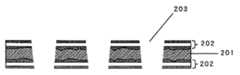
図1は、本発明における離型性フィルムの基本構成図である。図1において、ベースフィルム101は本発明の離型性フィルムの主要構成要であり、ポリエチレン、ポリプロピレン、ポリスチレン、ポリ塩化ビニル、ポリ塩化ビニリデン、ポリアミド、ポリエチレンテレフタレート、ポリブチレンテレフタレート、ポリアセタール、ポリカーボネート、ポリフェニレンオキサイド、ポリエチレンナフタレート、ポリフェニレンサルファイド、PTFE、ポリスルホン、ポリエーテルスルホン、ポリエーテルイミド、ポリエーテルエーテルケトン、ポリアミドイミド、全芳香族ポリエステル(LCP)、熱可塑性ポリイミド等の樹脂フィルムが利用できる。(Embodiment 1)
FIG. 1 is a basic configuration diagram of a releasable film in the present invention. In FIG. 1, a
このフィルムの厚みは3μm〜50μm程度のものが用いられる。厚い方が剛性が高くなり、取り扱い性が向上するが、あまり厚いとラミネートする際に熱が伝わりにくく、また曲げにくくロール状にしにくいため好ましくない場合がある。 The film has a thickness of about 3 μm to 50 μm. A thicker one increases rigidity and improves handleability. However, if it is too thick, heat may not be transmitted when laminating, and it may be difficult to bend and form a roll.
本発明の離型性フィルムは、前記ベースフィルム101の片側に熱可塑性樹脂層102を設けている。この熱可塑性樹脂層102には、メチルセルロース、エチルセルロース、ベンジルセルロース、トリアセチルセルロース、ニトロセルロースから選ばれる繊維素系樹脂または酢酸ビニル、ポリウレタン、アクリル酸エステル樹脂等の合成樹脂等を利用することができる。この熱可塑性樹脂層102は、塗工、ラミネート等の既存の方法により形成する事ができる。また、本発明の離型性フィルムを構成する熱可塑性樹脂層は、必要に応じてその表面をシリコン処理等の離型処理することができる。 In the releasable film of the present invention, a
熱可塑性樹脂層の厚みは3μm〜20μmであることが望ましい。これはあまり薄すぎるとプリプレグ表面の凹凸を吸収しきれず、また厚すぎると熱可塑性樹脂を軟化させるのに大量の熱エネルギーを要し不経済であるだけでなく、厚み方向に熱の伝わり方が不均一になりやすく、全面を完全に密着させることが難しいためである。 The thickness of the thermoplastic resin layer is desirably 3 μm to 20 μm. If it is too thin, it will not absorb the unevenness of the prepreg surface. This is because it is likely to be non-uniform and it is difficult to completely adhere the entire surface.
さらに熱可塑性樹脂層102には、必要に応じて無機フィラーを添加することができる。添加可能な無機フィラーとしては、SiO2、TiO2、Al2O3、BaSO4、Fe2O3、MgO、ZnO、CaCO3、Al(OH)3、Mg(OH)2などを用いることができる。Furthermore, an inorganic filler can be added to the
熱可塑性樹脂層に無機フィラーを添加することにより、更なる剛性向上と熱伝導性の確保ができるという効果がある。添加量としては熱硬化性樹脂中に30vol.%程度混入することが望ましい。この添加量は多いと剛性向上や、熱伝導率の向上には効果的であるが、多すぎると熱硬化性樹脂層が脆くなり割れてしまったり、粉塵が発生するといった問題がある。逆に少なすぎると剛性向上や、熱伝導率の向上という効果をなさなくなる。 By adding an inorganic filler to the thermoplastic resin layer, there is an effect that the rigidity can be further improved and the thermal conductivity can be ensured. As an addition amount, it is desirable to mix about 30 vol.% In the thermosetting resin. If the amount added is large, it is effective for improving rigidity and thermal conductivity, but if it is too large, there is a problem that the thermosetting resin layer becomes brittle and cracks or dust is generated. On the other hand, if the amount is too small, the effect of improving rigidity and improving thermal conductivity will not be achieved.
図2は、本発明の実施の形態1における離型性フィルムの構成図である。図2においてベースフィルム101および熱可塑性樹脂層102は、図1の構成と同じであり、熱可塑性樹脂層102の反対面に熱硬化性樹脂層103を設けている。この熱硬化性樹脂層103には、フェノール樹脂、尿素樹脂、メラミン樹脂、アルキッド樹脂、ケイ素樹脂、フラン樹脂、不飽和ポリエステル樹脂、エポキシ樹脂、ポリウレタン樹脂などから選ばれる熱硬化性樹脂を利用することができる。 FIG. 2 is a configuration diagram of the releasable film in the first embodiment of the present invention. In FIG. 2, the
ベースフィルムに熱硬化性樹脂層103を設けることにより、本離型フィルムを用いた回路基板の製造工程において、レーザー等の高エネルギービームによる貫通孔形成時の熱により発生する、離型フィルムの縮退や、はがれ、浮きを防止できる。 By providing the
この熱硬化性樹脂層は厚いほど剛性が高くなりしわの発生を抑えたり、寸法変化を抑えたりという効果が絶大であるが、あまり厚くなり過ぎると加熱工程にて熱可塑性樹脂層に熱が伝わりにくくなるため、適切な厚さにコントロールすることが重要である。この厚みは0.5μm〜3.0μmの範囲にすることが好ましい。熱硬化性樹脂の厚みをこの範囲にすると、しわの入りにくさおよび寸法変化の抑制と加熱時の熱の伝わり易さを適切にバランスすることができる。 The thicker the thermosetting resin layer, the higher the rigidity and the greater the effect of suppressing the generation of wrinkles and the reduction of dimensional change. However, if the layer is too thick, heat is transferred to the thermoplastic resin layer during the heating process. It is important to control the thickness appropriately. This thickness is preferably in the range of 0.5 μm to 3.0 μm. When the thickness of the thermosetting resin is within this range, it is possible to appropriately balance the difficulty of wrinkling and suppression of dimensional change and the ease of heat transfer during heating.
また、熱硬化性樹脂層103には、必要に応じて無機フィラーを添加することが望ましい。添加可能な無機フィラーとしては、SiO2、TiO2、Al2O3、BaSO4、Fe2O3、MgO、ZnO、CaCO3、Al(OH)3、Mg(OH)2などを用いることができる。Moreover, it is desirable to add an inorganic filler to the
熱硬化性樹脂層に無機フィラーを添加することにより更なる剛性向上が可能となるという効果がある。添加量としては熱硬化性樹脂中に30vol.%程度混入することによりこの効果は発現させることができる。 By adding an inorganic filler to the thermosetting resin layer, there is an effect that the rigidity can be further improved. This effect can be expressed by adding about 30 vol.% In the thermosetting resin as an addition amount.
またこの無機フィラーの添加により、剛性が向上し、しわが入りにくくなり、寸法安定性が向上するだけでなく、熱が伝わり易くなり、加熱ラミネート工程が容易になるという効果も発現できる。この場合は熱硬化性樹脂層の厚みを無機フィラーがない場合と比較して大きくすることができ、更なる剛性および寸法安定性の向上が図れると同時に、加熱ラミネートも低温、短時間行うことができ、ラミネータの消費電力を削減できるため生産効率も向上する。 In addition, the addition of the inorganic filler can improve the rigidity, make it difficult to wrinkle, improve not only the dimensional stability, but also facilitate the heat lamination and facilitate the heating lamination process. In this case, the thickness of the thermosetting resin layer can be increased as compared with the case where there is no inorganic filler, and the rigidity and dimensional stability can be further improved, and at the same time, the heating lamination can be performed at a low temperature for a short time. It is possible to reduce the power consumption of the laminator and improve the production efficiency.
また、無機フィラーの添加により熱が伝わり易くなるため、無機フィラーが無い場合と比較して熱可塑性樹脂に加わる熱が安定し、安定した貼り付けが可能となるため、さらに高精度な、例えばビア径100μm以下という基板の作成が容易となり、製造上の歩留まりも向上する。 In addition, since heat is easily transmitted by the addition of the inorganic filler, the heat applied to the thermoplastic resin is stable compared to the case where there is no inorganic filler, and stable pasting is possible. Fabrication of a substrate having a diameter of 100 μm or less is facilitated, and the manufacturing yield is improved.
また、無機フィラーの添加により熱が伝わり易くなるため、熱硬化性樹脂層の厚みを大きくでき、更に剛性や取り扱い易さおよび寸法安定性が向上する。 In addition, since heat is easily transmitted by the addition of the inorganic filler, the thickness of the thermosetting resin layer can be increased, and rigidity, ease of handling, and dimensional stability are improved.
また、熱硬化性樹脂層の厚みを大きくすることができるだけでなく、熱硬化性樹脂層の厚みをシビアにコントロールする必要が無くなり、加熱ラミネート工程において貼り付け性能のよい離型性フィルムを容易に得ることができる。 In addition, not only can the thickness of the thermosetting resin layer be increased, but it is not necessary to control the thickness of the thermosetting resin layer severely, making it easy to obtain a releasable film with good pasting performance in the heat laminating process. Can be obtained.
かかる構成によれば、図5の様に凹凸を持つプリプレグ201の両面に本発明の離型性フィルム202を配し、ラミネートロール210により加熱加圧して貼り合わせることができる。この場合、図3に示すように、本発明の離型性フィルム202に設けた熱可塑性樹脂層102をプリプレグ201側に配置する。ラミネート時の熱により、熱可塑性樹脂層102が軟化、変形することにより、プリプレグ201の表面凹凸に沿って密着し、本発明のフィルム付き基材を得ることができる。 According to this configuration, the
このときの加熱条件としては、用いている熱可塑性樹脂の軟化温度以上の温度で加熱することが望ましい。 As heating conditions at this time, it is desirable to heat at a temperature equal to or higher than the softening temperature of the thermoplastic resin used.
ここで、本発明で用いられるプリプレグ201は芯材と熱硬化性樹脂より構成される。芯材にはガラス繊維などの無機繊維または、アラミド、液晶ポリマー、PTFEなどの有機繊維による織布または不織布が用いられる。熱硬化性樹脂にはフェノール樹脂、尿素樹脂、メラミン樹脂、アルキッド樹脂、ケイ素樹脂、フラン樹脂、不飽和ポリエステル樹脂、エポキシ樹脂、ポリウレタン樹脂、シアネートエステル樹脂、ポリイミド樹脂などを利用することができ、芯材と複合化され、半硬化状態になっている。ここで、熱硬化性樹脂中に、SiO2、TiO2、Al2O3、BaSO4、Fe2O3、MgO、ZnO、CaCO3、Al(OH)3、Mg(OH)2などの無機フィラーを必要に応じて添加することができる。Here, the
また、図4に示すフィルム付き基材の任意の場所に、必要に応じて貫通孔203を形成することができる。貫通孔203の形成方法はドリル加工、レーザー加工など公知の加工法により実施することができる。この時、離型性フィルム202に熱硬化性樹脂層103があると、離型性フィルム202の剛性が高くなり、熱による寸法変化を起こしにくくなるので好ましい。 Moreover, the through-
また、レーザーによる穴加工を行う場合、離型性フィルム202を構成するベースフィルム101、熱可塑性樹脂層102、熱硬化性樹脂層103の少なくとも一つに波長が11.0μmから0.2μmの範囲の光を吸収する光吸収剤を添加することが好ましい。 In addition, when drilling with a laser, at least one of the
光吸収剤としては、紫外線吸収剤(JF−77:城北化学工業製:添加量1重量部)を本実施の形態では用いたが、その他の材料としては、ベンゾトリアゾール類やベンゾフェノン類などをはじめとする公知の紫外線吸収剤を用いることができる。 As the light absorber, an ultraviolet absorber (JF-77: manufactured by Johoku Chemical Industry Co., Ltd .: 1 part by weight) was used in this embodiment, but other materials include benzotriazoles and benzophenones. The well-known ultraviolet absorber can be used.
ベンゾトリアゾール類からなる紫外線吸収剤としては、例えば、2−(2’−ヒドロキシ−5’−メチルフェニル)−ベンゾトリアゾール、2−(2’−ヒドロキシ−3’−tert−ブチル−5’−メチルフェニル)−5−クロロベンゾトリアゾール、6−(2−ベンゾトリアゾリル)−4−t−オクチル−6’−t−ブチル−4’−メチル−2,2’−メチレンビスフェノール等がある。 Examples of ultraviolet absorbers composed of benzotriazoles include 2- (2′-hydroxy-5′-methylphenyl) -benzotriazole and 2- (2′-hydroxy-3′-tert-butyl-5′-methyl). Phenyl) -5-chlorobenzotriazole, 6- (2-benzotriazolyl) -4-t-octyl-6'-t-butyl-4'-methyl-2,2'-methylenebisphenol, and the like.
ベンゾフェノン類からなる紫外線吸収剤としては、2,2’−ジヒドロキシ−4,4’−ジメトキシ−ベンゾフェノン、2,2’,4,4’−テトラヒドロキシ−ベンゾフェノン等がある。 Examples of ultraviolet absorbers composed of benzophenones include 2,2'-dihydroxy-4,4'-dimethoxy-benzophenone and 2,2 ', 4,4'-tetrahydroxy-benzophenone.
これらを用いて、紫外線領域以下の波長のレーザー光に対する光吸収性を備えることが可能となる。 By using these, it becomes possible to provide light absorptivity with respect to laser light having a wavelength shorter than the ultraviolet region.
この光吸収剤はベースフィルム、熱可塑性樹脂層、熱硬化性樹脂層の少なくとも一つの層に1〜10重量%程度を入れることが好ましい。 The light absorber is preferably added in an amount of about 1 to 10% by weight in at least one of a base film, a thermoplastic resin layer, and a thermosetting resin layer.
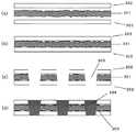
本発明の離型性フィルムおよびフィルム付き基材を用いた回路基板の製造方法を図6に示す。 FIG. 6 shows a method for producing a circuit board using the releasable film and the substrate with film of the present invention.
図6(a)に示すようにプリプレグ201の上下の両面に本発明の離型フィルム202を配置し、プリプレグ201の両面に本発明の離型性フィルム202(プリプレグ側に熱可塑性樹脂層を配置)を貼り合わせ、図6(b)に示すフィルム付き基材を得る。 6A, the
次に図6(c)に示すように、フィルム付き基材に炭酸ガスレーザーを用いて貫通孔303を形成した。 Next, as shown in FIG.6 (c), the through-
次に図6(d)に示すように、スクリーン印刷の手法を用いて貫通孔303に導電性ペースト304を充填した。 Next, as shown in FIG. 6D, the through-
次に図6(e)に示すように、両面の離型性フィルム202を剥離する。この場合、離型性フィルムを構成する外側の層から順次剥離することにより、導電性ペースト充填量の減少を抑制することができる。この剥離の際に、離型性フィルム側にプリプレグの樹脂が一部転写してもかまわない。 Next, as shown in FIG.6 (e), the double-
次に図6(f)に示すように、両面に電解銅箔305を配置する。これを真空熱プレスする事により、図6(g)に示す両面接続体を得ることができる。 Next, as shown in FIG.6 (f), the
最後に図6(h)に示すように、両面の銅箔をフォトリソ、エッチングにより所望の回路パターン306を形成することにより、両面基板を得ることができる。 Finally, as shown in FIG. 6 (h), a double-sided substrate can be obtained by forming a desired circuit pattern 306 by photolithography and etching of copper foils on both sides.
また、図6の(h)に示す両面基板をコアとして、導電性ペーストが充填されたプリプレグ図6(e)を両面に配置し、さらにその外側に電解銅箔を配置して図6(f)〜(h)と同様の真空熱プレス、フォトリソ、エッチングを繰り返すことにより多層基板を製造することができる。 Further, with the double-sided substrate shown in FIG. 6 (h) as the core, the prepreg FIG. 6 (e) filled with the conductive paste is arranged on both sides, and an electrolytic copper foil is further arranged on the outside thereof, and FIG. ) To (h), a multilayer substrate can be produced by repeating the same vacuum hot pressing, photolithography, and etching.
本発明の離型性フィルム、フィルム付き基材を用いることにより、凹凸を有するプリプレグとの十分な密着性を確保することが可能となり、導電性ペーストによる層間接続を実現する高精度な回路基板を得ることができる。 By using the releasable film and the substrate with film of the present invention, it becomes possible to ensure sufficient adhesion with the prepreg having irregularities, and a highly accurate circuit board that realizes interlayer connection with a conductive paste. Can be obtained.
本発明にかかる離型性フィルムは、凹凸を持つ軟化温度の高い絶縁基材との熱ラミネートにおいて優れた密着性を示し、その後の穴加工や導電性ペースト印刷等において安定したものづくりが可能となる。本発明は導電性ペースト接続による回路基板だけでなく、他の方式による回路基板製造にも応用できる。 The releasable film according to the present invention exhibits excellent adhesion in thermal lamination with an insulating substrate having unevenness and a high softening temperature, and enables stable manufacturing in subsequent drilling or conductive paste printing. . The present invention can be applied not only to circuit boards using conductive paste connection, but also to circuit board manufacture using other methods.
101 ベースフィルム
102 熱可塑性樹脂層
103 熱硬化性樹脂層
201 プリプレグ(多孔質基材)
202 本発明の離型性フィルム
203 貫通穴
210 ラミネートロール
204 導電性ペースト
205 銅箔
206 回路パターン
301 プリプレグ(多孔質基材)
302 従来の離型性フィルム
303 加工穴
304 導電性ペースト
305 導電性ペーストにじみDESCRIPTION OF
202 Release film of the
302 Conventional
Claims (17)
Translated fromJapanesePriority Applications (1)
| Application Number | Priority Date | Filing Date | Title |
|---|---|---|---|
| JP2004025207AJP2005212428A (en) | 2004-02-02 | 2004-02-02 | Release film, substrate with film, method for producing the same, and method for producing circuit board |
Applications Claiming Priority (1)
| Application Number | Priority Date | Filing Date | Title |
|---|---|---|---|
| JP2004025207AJP2005212428A (en) | 2004-02-02 | 2004-02-02 | Release film, substrate with film, method for producing the same, and method for producing circuit board |
Publications (1)
| Publication Number | Publication Date |
|---|---|
| JP2005212428Atrue JP2005212428A (en) | 2005-08-11 |
Family
ID=34907648
Family Applications (1)
| Application Number | Title | Priority Date | Filing Date |
|---|---|---|---|
| JP2004025207AWithdrawnJP2005212428A (en) | 2004-02-02 | 2004-02-02 | Release film, substrate with film, method for producing the same, and method for producing circuit board |
Country Status (1)
| Country | Link |
|---|---|
| JP (1) | JP2005212428A (en) |
Cited By (7)
| Publication number | Priority date | Publication date | Assignee | Title |
|---|---|---|---|---|
| JP2006281481A (en)* | 2005-03-31 | 2006-10-19 | Lintec Corp | Process film for manufacturing laminated circuit boards |
| JP2009200205A (en)* | 2008-02-21 | 2009-09-03 | Panasonic Corp | Circuit board, inspecting method for circuit board, and manufacturing method of circuit board |
| JP2009220556A (en)* | 2008-03-18 | 2009-10-01 | Samsung Electro Mech Co Ltd | Method of manufacturing insulating sheet, metal laminate using the same, and method of manufacturing printed circuit board |
| JP2009283929A (en)* | 2008-04-25 | 2009-12-03 | Semiconductor Energy Lab Co Ltd | Manufacturing process of semiconductor device and semiconductor device |
| JP2010194841A (en)* | 2009-02-25 | 2010-09-09 | Sekisui Chem Co Ltd | Release film and method for manufacturing the same |
| CN104945875A (en)* | 2015-05-29 | 2015-09-30 | 吉翔宝(太仓)离型材料科技发展有限公司 | Polycarbonate release film |
| WO2022088274A1 (en)* | 2020-10-27 | 2022-05-05 | 瑞声声学科技(深圳)有限公司 | Metal plastic composite film, preparation method therefor and use thereof |
- 2004
- 2004-02-02JPJP2004025207Apatent/JP2005212428A/ennot_activeWithdrawn
Cited By (9)
| Publication number | Priority date | Publication date | Assignee | Title |
|---|---|---|---|---|
| JP2006281481A (en)* | 2005-03-31 | 2006-10-19 | Lintec Corp | Process film for manufacturing laminated circuit boards |
| JP2009200205A (en)* | 2008-02-21 | 2009-09-03 | Panasonic Corp | Circuit board, inspecting method for circuit board, and manufacturing method of circuit board |
| JP2009220556A (en)* | 2008-03-18 | 2009-10-01 | Samsung Electro Mech Co Ltd | Method of manufacturing insulating sheet, metal laminate using the same, and method of manufacturing printed circuit board |
| JP2009283929A (en)* | 2008-04-25 | 2009-12-03 | Semiconductor Energy Lab Co Ltd | Manufacturing process of semiconductor device and semiconductor device |
| US8637932B2 (en) | 2008-04-25 | 2014-01-28 | Semiconductor Energy Laboratory Co., Ltd. | Semiconductor device and method for manufacturing the same |
| US9171808B2 (en) | 2008-04-25 | 2015-10-27 | Semiconductor Energy Laboratory Co., Ltd. | Semiconductor device and method for manufacturing the same |
| JP2010194841A (en)* | 2009-02-25 | 2010-09-09 | Sekisui Chem Co Ltd | Release film and method for manufacturing the same |
| CN104945875A (en)* | 2015-05-29 | 2015-09-30 | 吉翔宝(太仓)离型材料科技发展有限公司 | Polycarbonate release film |
| WO2022088274A1 (en)* | 2020-10-27 | 2022-05-05 | 瑞声声学科技(深圳)有限公司 | Metal plastic composite film, preparation method therefor and use thereof |
Similar Documents
| Publication | Publication Date | Title |
|---|---|---|
| US6734375B2 (en) | Circuit board having an interstitial inner via hole structure | |
| JP4288266B2 (en) | Manufacturing method of printed circuit board with built-in multilayer capacitor | |
| JP5093353B2 (en) | Manufacturing method of component built-in module and component built-in module | |
| TW200906263A (en) | Circuit board and method for manufacturing the same | |
| US20140374153A1 (en) | Printed circuit board and method for manufacturing same | |
| WO2007114111A1 (en) | Multilayer wiring board and its manufacturing method | |
| JP2008124370A (en) | Method of manufacturing multilayer printed wiring board | |
| US20040214006A1 (en) | Member for a circuit board, method of manufacturing the same, and methods of manufacturing circuit boards | |
| JP4348815B2 (en) | Method for manufacturing printed wiring board | |
| KR101056898B1 (en) | Multilayer printed circuit board and its manufacturing method | |
| JP2005212428A (en) | Release film, substrate with film, method for producing the same, and method for producing circuit board | |
| JP2004343086A (en) | Circuit board member, method of manufacturing the same, and method of manufacturing a circuit board | |
| JP2009246336A (en) | Wiring board and method of making the same | |
| US20130062099A1 (en) | Multiple layer z-axis interconnect apparatus and method of use | |
| JP3760771B2 (en) | Circuit forming substrate and method of manufacturing circuit forming substrate | |
| JP4797742B2 (en) | Multilayer wiring board and manufacturing method thereof | |
| JP2006176677A (en) | Composite, prepreg using the same, metallic foil lined laminate, printed wiring substrate and method for manufacturing printed wiring substrate | |
| JP4395741B2 (en) | Multilayer substrate manufacturing method | |
| JP2007266165A (en) | Manufacturing method of multilayer wiring board | |
| JP2006222182A (en) | Rigid flexible substrate | |
| JP2006160899A (en) | Electrically insulating substrate and method for manufacturing wiring substrate | |
| JP2002103494A (en) | Prepreg, printed wiring board and method of manufacturing the same | |
| KR20050112365A (en) | Flat coating process with utilizing a resin coated copper for printed circuit board | |
| JP2005045008A (en) | Multilayer laminate and method for producing the same | |
| JP4797743B2 (en) | Manufacturing method of multilayer wiring board |
Legal Events
| Date | Code | Title | Description |
|---|---|---|---|
| A621 | Written request for application examination | Free format text:JAPANESE INTERMEDIATE CODE: A621 Effective date:20061030 | |
| RD01 | Notification of change of attorney | Free format text:JAPANESE INTERMEDIATE CODE: A7421 Effective date:20061114 | |
| A761 | Written withdrawal of application | Free format text:JAPANESE INTERMEDIATE CODE: A761 Effective date:20061205 |