JP2005211946A - Solder alloy and semiconductor device - Google Patents
Solder alloy and semiconductor deviceDownload PDFInfo
- Publication number
- JP2005211946A JP2005211946AJP2004022598AJP2004022598AJP2005211946AJP 2005211946 AJP2005211946 AJP 2005211946AJP 2004022598 AJP2004022598 AJP 2004022598AJP 2004022598 AJP2004022598 AJP 2004022598AJP 2005211946 AJP2005211946 AJP 2005211946A
- Authority
- JP
- Japan
- Prior art keywords
- solder
- semiconductor device
- mass
- solder alloy
- package substrate
- Prior art date
- Legal status (The legal status is an assumption and is not a legal conclusion. Google has not performed a legal analysis and makes no representation as to the accuracy of the status listed.)
- Pending
Links
- 229910000679solderInorganic materials0.000titleclaimsabstractdescription61
- 239000004065semiconductorSubstances0.000titleclaimsabstractdescription50
- 229910045601alloyInorganic materials0.000titleclaimsabstractdescription23
- 239000000956alloySubstances0.000titleclaimsabstractdescription23
- 229910052802copperInorganic materials0.000claimsabstractdescription12
- 239000000758substrateSubstances0.000abstractdescription18
- 229910052709silverInorganic materials0.000abstractdescription4
- 239000010949copperSubstances0.000description14
- 229920005989resinPolymers0.000description8
- 239000011347resinSubstances0.000description8
- 239000003351stiffenerSubstances0.000description8
- 239000000203mixtureSubstances0.000description6
- 239000002390adhesive tapeSubstances0.000description5
- 238000002474experimental methodMethods0.000description5
- 238000000034methodMethods0.000description4
- 238000012986modificationMethods0.000description4
- 230000004048modificationEffects0.000description4
- 230000035882stressEffects0.000description3
- RYGMFSIKBFXOCR-UHFFFAOYSA-NCopperChemical compound[Cu]RYGMFSIKBFXOCR-UHFFFAOYSA-N0.000description2
- BQCADISMDOOEFD-UHFFFAOYSA-NSilverChemical compound[Ag]BQCADISMDOOEFD-UHFFFAOYSA-N0.000description2
- 230000000694effectsEffects0.000description2
- 239000003822epoxy resinSubstances0.000description2
- 230000017525heat dissipationEffects0.000description2
- 229920000647polyepoxidePolymers0.000description2
- 239000004332silverSubstances0.000description2
- 229910052718tinInorganic materials0.000description2
- 229910001128Sn alloyInorganic materials0.000description1
- ATJFFYVFTNAWJD-UHFFFAOYSA-NTinChemical compound[Sn]ATJFFYVFTNAWJD-UHFFFAOYSA-N0.000description1
- 230000002411adverseEffects0.000description1
- 230000003247decreasing effectEffects0.000description1
- 230000008021depositionEffects0.000description1
- 238000010586diagramMethods0.000description1
- 230000005496eutecticsEffects0.000description1
- 230000006355external stressEffects0.000description1
- 230000010354integrationEffects0.000description1
- 230000005855radiationEffects0.000description1
- 239000012779reinforcing materialSubstances0.000description1
Images


Classifications
- H—ELECTRICITY
- H01—ELECTRIC ELEMENTS
- H01L—SEMICONDUCTOR DEVICES NOT COVERED BY CLASS H10
- H01L24/00—Arrangements for connecting or disconnecting semiconductor or solid-state bodies; Methods or apparatus related thereto
- H01L24/01—Means for bonding being attached to, or being formed on, the surface to be connected, e.g. chip-to-package, die-attach, "first-level" interconnects; Manufacturing methods related thereto
- H01L24/10—Bump connectors ; Manufacturing methods related thereto
- H01L24/12—Structure, shape, material or disposition of the bump connectors prior to the connecting process
- H01L24/13—Structure, shape, material or disposition of the bump connectors prior to the connecting process of an individual bump connector
- H—ELECTRICITY
- H01—ELECTRIC ELEMENTS
- H01L—SEMICONDUCTOR DEVICES NOT COVERED BY CLASS H10
- H01L21/00—Processes or apparatus adapted for the manufacture or treatment of semiconductor or solid state devices or of parts thereof
- H01L21/02—Manufacture or treatment of semiconductor devices or of parts thereof
- H01L21/04—Manufacture or treatment of semiconductor devices or of parts thereof the devices having potential barriers, e.g. a PN junction, depletion layer or carrier concentration layer
- H01L21/50—Assembly of semiconductor devices using processes or apparatus not provided for in a single one of the groups H01L21/18 - H01L21/326 or H10D48/04 - H10D48/07 e.g. sealing of a cap to a base of a container
- H01L21/56—Encapsulations, e.g. encapsulation layers, coatings
- H01L21/563—Encapsulation of active face of flip-chip device, e.g. underfilling or underencapsulation of flip-chip, encapsulation preform on chip or mounting substrate
- H—ELECTRICITY
- H01—ELECTRIC ELEMENTS
- H01L—SEMICONDUCTOR DEVICES NOT COVERED BY CLASS H10
- H01L2224/00—Indexing scheme for arrangements for connecting or disconnecting semiconductor or solid-state bodies and methods related thereto as covered by H01L24/00
- H01L2224/01—Means for bonding being attached to, or being formed on, the surface to be connected, e.g. chip-to-package, die-attach, "first-level" interconnects; Manufacturing methods related thereto
- H01L2224/02—Bonding areas; Manufacturing methods related thereto
- H01L2224/04—Structure, shape, material or disposition of the bonding areas prior to the connecting process
- H01L2224/05—Structure, shape, material or disposition of the bonding areas prior to the connecting process of an individual bonding area
- H01L2224/0554—External layer
- H01L2224/0556—Disposition
- H01L2224/05568—Disposition the whole external layer protruding from the surface
- H—ELECTRICITY
- H01—ELECTRIC ELEMENTS
- H01L—SEMICONDUCTOR DEVICES NOT COVERED BY CLASS H10
- H01L2224/00—Indexing scheme for arrangements for connecting or disconnecting semiconductor or solid-state bodies and methods related thereto as covered by H01L24/00
- H01L2224/01—Means for bonding being attached to, or being formed on, the surface to be connected, e.g. chip-to-package, die-attach, "first-level" interconnects; Manufacturing methods related thereto
- H01L2224/02—Bonding areas; Manufacturing methods related thereto
- H01L2224/04—Structure, shape, material or disposition of the bonding areas prior to the connecting process
- H01L2224/05—Structure, shape, material or disposition of the bonding areas prior to the connecting process of an individual bonding area
- H01L2224/0554—External layer
- H01L2224/05573—Single external layer
- H—ELECTRICITY
- H01—ELECTRIC ELEMENTS
- H01L—SEMICONDUCTOR DEVICES NOT COVERED BY CLASS H10
- H01L2224/00—Indexing scheme for arrangements for connecting or disconnecting semiconductor or solid-state bodies and methods related thereto as covered by H01L24/00
- H01L2224/01—Means for bonding being attached to, or being formed on, the surface to be connected, e.g. chip-to-package, die-attach, "first-level" interconnects; Manufacturing methods related thereto
- H01L2224/10—Bump connectors; Manufacturing methods related thereto
- H01L2224/12—Structure, shape, material or disposition of the bump connectors prior to the connecting process
- H01L2224/13—Structure, shape, material or disposition of the bump connectors prior to the connecting process of an individual bump connector
- H01L2224/13001—Core members of the bump connector
- H01L2224/13099—Material
- H—ELECTRICITY
- H01—ELECTRIC ELEMENTS
- H01L—SEMICONDUCTOR DEVICES NOT COVERED BY CLASS H10
- H01L2224/00—Indexing scheme for arrangements for connecting or disconnecting semiconductor or solid-state bodies and methods related thereto as covered by H01L24/00
- H01L2224/01—Means for bonding being attached to, or being formed on, the surface to be connected, e.g. chip-to-package, die-attach, "first-level" interconnects; Manufacturing methods related thereto
- H01L2224/10—Bump connectors; Manufacturing methods related thereto
- H01L2224/15—Structure, shape, material or disposition of the bump connectors after the connecting process
- H01L2224/16—Structure, shape, material or disposition of the bump connectors after the connecting process of an individual bump connector
- H01L2224/161—Disposition
- H01L2224/16151—Disposition the bump connector connecting between a semiconductor or solid-state body and an item not being a semiconductor or solid-state body, e.g. chip-to-substrate, chip-to-passive
- H01L2224/16221—Disposition the bump connector connecting between a semiconductor or solid-state body and an item not being a semiconductor or solid-state body, e.g. chip-to-substrate, chip-to-passive the body and the item being stacked
- H01L2224/16225—Disposition the bump connector connecting between a semiconductor or solid-state body and an item not being a semiconductor or solid-state body, e.g. chip-to-substrate, chip-to-passive the body and the item being stacked the item being non-metallic, e.g. insulating substrate with or without metallisation
- H—ELECTRICITY
- H01—ELECTRIC ELEMENTS
- H01L—SEMICONDUCTOR DEVICES NOT COVERED BY CLASS H10
- H01L2224/00—Indexing scheme for arrangements for connecting or disconnecting semiconductor or solid-state bodies and methods related thereto as covered by H01L24/00
- H01L2224/01—Means for bonding being attached to, or being formed on, the surface to be connected, e.g. chip-to-package, die-attach, "first-level" interconnects; Manufacturing methods related thereto
- H01L2224/26—Layer connectors, e.g. plate connectors, solder or adhesive layers; Manufacturing methods related thereto
- H01L2224/31—Structure, shape, material or disposition of the layer connectors after the connecting process
- H01L2224/32—Structure, shape, material or disposition of the layer connectors after the connecting process of an individual layer connector
- H01L2224/321—Disposition
- H01L2224/32151—Disposition the layer connector connecting between a semiconductor or solid-state body and an item not being a semiconductor or solid-state body, e.g. chip-to-substrate, chip-to-passive
- H01L2224/32221—Disposition the layer connector connecting between a semiconductor or solid-state body and an item not being a semiconductor or solid-state body, e.g. chip-to-substrate, chip-to-passive the body and the item being stacked
- H01L2224/32225—Disposition the layer connector connecting between a semiconductor or solid-state body and an item not being a semiconductor or solid-state body, e.g. chip-to-substrate, chip-to-passive the body and the item being stacked the item being non-metallic, e.g. insulating substrate with or without metallisation
- H—ELECTRICITY
- H01—ELECTRIC ELEMENTS
- H01L—SEMICONDUCTOR DEVICES NOT COVERED BY CLASS H10
- H01L2224/00—Indexing scheme for arrangements for connecting or disconnecting semiconductor or solid-state bodies and methods related thereto as covered by H01L24/00
- H01L2224/73—Means for bonding being of different types provided for in two or more of groups H01L2224/10, H01L2224/18, H01L2224/26, H01L2224/34, H01L2224/42, H01L2224/50, H01L2224/63, H01L2224/71
- H01L2224/732—Location after the connecting process
- H01L2224/73201—Location after the connecting process on the same surface
- H01L2224/73203—Bump and layer connectors
- H01L2224/73204—Bump and layer connectors the bump connector being embedded into the layer connector
- H—ELECTRICITY
- H01—ELECTRIC ELEMENTS
- H01L—SEMICONDUCTOR DEVICES NOT COVERED BY CLASS H10
- H01L2224/00—Indexing scheme for arrangements for connecting or disconnecting semiconductor or solid-state bodies and methods related thereto as covered by H01L24/00
- H01L2224/73—Means for bonding being of different types provided for in two or more of groups H01L2224/10, H01L2224/18, H01L2224/26, H01L2224/34, H01L2224/42, H01L2224/50, H01L2224/63, H01L2224/71
- H01L2224/732—Location after the connecting process
- H01L2224/73251—Location after the connecting process on different surfaces
- H01L2224/73253—Bump and layer connectors
- H—ELECTRICITY
- H01—ELECTRIC ELEMENTS
- H01L—SEMICONDUCTOR DEVICES NOT COVERED BY CLASS H10
- H01L23/00—Details of semiconductor or other solid state devices
- H01L23/16—Fillings or auxiliary members in containers or encapsulations, e.g. centering rings
- H—ELECTRICITY
- H01—ELECTRIC ELEMENTS
- H01L—SEMICONDUCTOR DEVICES NOT COVERED BY CLASS H10
- H01L23/00—Details of semiconductor or other solid state devices
- H01L23/34—Arrangements for cooling, heating, ventilating or temperature compensation ; Temperature sensing arrangements
- H01L23/36—Selection of materials, or shaping, to facilitate cooling or heating, e.g. heatsinks
- H—ELECTRICITY
- H01—ELECTRIC ELEMENTS
- H01L—SEMICONDUCTOR DEVICES NOT COVERED BY CLASS H10
- H01L2924/00—Indexing scheme for arrangements or methods for connecting or disconnecting semiconductor or solid-state bodies as covered by H01L24/00
- H01L2924/0001—Technical content checked by a classifier
- H01L2924/00014—Technical content checked by a classifier the subject-matter covered by the group, the symbol of which is combined with the symbol of this group, being disclosed without further technical details
- H—ELECTRICITY
- H01—ELECTRIC ELEMENTS
- H01L—SEMICONDUCTOR DEVICES NOT COVERED BY CLASS H10
- H01L2924/00—Indexing scheme for arrangements or methods for connecting or disconnecting semiconductor or solid-state bodies as covered by H01L24/00
- H01L2924/01—Chemical elements
- H01L2924/01006—Carbon [C]
- H—ELECTRICITY
- H01—ELECTRIC ELEMENTS
- H01L—SEMICONDUCTOR DEVICES NOT COVERED BY CLASS H10
- H01L2924/00—Indexing scheme for arrangements or methods for connecting or disconnecting semiconductor or solid-state bodies as covered by H01L24/00
- H01L2924/01—Chemical elements
- H01L2924/01029—Copper [Cu]
- H—ELECTRICITY
- H01—ELECTRIC ELEMENTS
- H01L—SEMICONDUCTOR DEVICES NOT COVERED BY CLASS H10
- H01L2924/00—Indexing scheme for arrangements or methods for connecting or disconnecting semiconductor or solid-state bodies as covered by H01L24/00
- H01L2924/01—Chemical elements
- H01L2924/01033—Arsenic [As]
- H—ELECTRICITY
- H01—ELECTRIC ELEMENTS
- H01L—SEMICONDUCTOR DEVICES NOT COVERED BY CLASS H10
- H01L2924/00—Indexing scheme for arrangements or methods for connecting or disconnecting semiconductor or solid-state bodies as covered by H01L24/00
- H01L2924/01—Chemical elements
- H01L2924/01047—Silver [Ag]
- H—ELECTRICITY
- H01—ELECTRIC ELEMENTS
- H01L—SEMICONDUCTOR DEVICES NOT COVERED BY CLASS H10
- H01L2924/00—Indexing scheme for arrangements or methods for connecting or disconnecting semiconductor or solid-state bodies as covered by H01L24/00
- H01L2924/01—Chemical elements
- H01L2924/01082—Lead [Pb]
- H—ELECTRICITY
- H01—ELECTRIC ELEMENTS
- H01L—SEMICONDUCTOR DEVICES NOT COVERED BY CLASS H10
- H01L2924/00—Indexing scheme for arrangements or methods for connecting or disconnecting semiconductor or solid-state bodies as covered by H01L24/00
- H01L2924/013—Alloys
- H01L2924/0132—Binary Alloys
- H01L2924/01322—Eutectic Alloys, i.e. obtained by a liquid transforming into two solid phases
- H—ELECTRICITY
- H01—ELECTRIC ELEMENTS
- H01L—SEMICONDUCTOR DEVICES NOT COVERED BY CLASS H10
- H01L2924/00—Indexing scheme for arrangements or methods for connecting or disconnecting semiconductor or solid-state bodies as covered by H01L24/00
- H01L2924/013—Alloys
- H01L2924/014—Solder alloys
- H—ELECTRICITY
- H01—ELECTRIC ELEMENTS
- H01L—SEMICONDUCTOR DEVICES NOT COVERED BY CLASS H10
- H01L2924/00—Indexing scheme for arrangements or methods for connecting or disconnecting semiconductor or solid-state bodies as covered by H01L24/00
- H01L2924/10—Details of semiconductor or other solid state devices to be connected
- H01L2924/11—Device type
- H01L2924/14—Integrated circuits
- H—ELECTRICITY
- H01—ELECTRIC ELEMENTS
- H01L—SEMICONDUCTOR DEVICES NOT COVERED BY CLASS H10
- H01L2924/00—Indexing scheme for arrangements or methods for connecting or disconnecting semiconductor or solid-state bodies as covered by H01L24/00
- H01L2924/15—Details of package parts other than the semiconductor or other solid state devices to be connected
- H01L2924/151—Die mounting substrate
- H01L2924/153—Connection portion
- H01L2924/1531—Connection portion the connection portion being formed only on the surface of the substrate opposite to the die mounting surface
- H01L2924/15311—Connection portion the connection portion being formed only on the surface of the substrate opposite to the die mounting surface being a ball array, e.g. BGA
- H—ELECTRICITY
- H01—ELECTRIC ELEMENTS
- H01L—SEMICONDUCTOR DEVICES NOT COVERED BY CLASS H10
- H01L2924/00—Indexing scheme for arrangements or methods for connecting or disconnecting semiconductor or solid-state bodies as covered by H01L24/00
- H01L2924/15—Details of package parts other than the semiconductor or other solid state devices to be connected
- H01L2924/161—Cap
- H01L2924/1615—Shape
- H01L2924/16195—Flat cap [not enclosing an internal cavity]
- H—ELECTRICITY
- H01—ELECTRIC ELEMENTS
- H01L—SEMICONDUCTOR DEVICES NOT COVERED BY CLASS H10
- H01L2924/00—Indexing scheme for arrangements or methods for connecting or disconnecting semiconductor or solid-state bodies as covered by H01L24/00
- H01L2924/15—Details of package parts other than the semiconductor or other solid state devices to be connected
- H01L2924/181—Encapsulation
Landscapes
- Engineering & Computer Science (AREA)
- Computer Hardware Design (AREA)
- Microelectronics & Electronic Packaging (AREA)
- Power Engineering (AREA)
- Wire Bonding (AREA)
Abstract
Description
Translated fromJapanese本発明は鉛フリー半田、並びに鉛フリー半田で形成されたバンプを備える半導体装置に関するものである。 The present invention relates to a lead-free solder and a semiconductor device including a bump formed of lead-free solder.
半導体装置の組立技術の1つとして、フリップチップボンディングが知られている。このボンディング方法は、半導体素子(半導体チップ)の下面に設けられた電極と、配線基板(パッケージ基板)上面に設けられた接続パッドとを密着させ、熱および圧力を加えて接合する方式である。その際、半導体チップの電極上およびパッケージ基板の接続パッド上には、予め半田バンプが形成されている。 Flip chip bonding is known as one of semiconductor device assembly techniques. This bonding method is a method in which an electrode provided on the lower surface of a semiconductor element (semiconductor chip) and a connection pad provided on an upper surface of a wiring substrate (package substrate) are brought into close contact with each other by applying heat and pressure. At that time, solder bumps are formed in advance on the electrodes of the semiconductor chip and on the connection pads of the package substrate.
従来、半田バンプに使用される半田としては、Sn(錫)−Pb(鉛)共晶半田が使用されていた。しかし近年では、電子部品を廃棄処理する際の環境への悪影響を抑制するために、半田合金としてPbを含まない、いわゆる鉛フリー半田が広く使用されている。 Conventionally, Sn (tin) -Pb (lead) eutectic solder has been used as solder used for solder bumps. However, in recent years, so-called lead-free solder that does not contain Pb as a solder alloy has been widely used in order to suppress adverse effects on the environment when electronic components are disposed of.
半田バンプに使用される鉛フリー半田としては、従来、Ag(銀):3〜4質量%、Cu(銅):0.5〜1.0質量%、残部はSnからなる半田合金が一般的であった。また、原材料価格的に高価なAgをさほど使用せず(2質量%以下)、接合信頼性、耐落下衝撃性に優れた半田バンプ用の半田合金も提案されている(例えば特許文献1)。 As a lead-free solder used for a solder bump, conventionally, a solder alloy made of Ag (silver): 3 to 4 mass%, Cu (copper): 0.5 to 1.0 mass%, and the balance being Sn is generally used. Met. In addition, a solder alloy for solder bumps has been proposed that does not use as much raw material-priced Ag (2% by mass or less) and has excellent bonding reliability and drop impact resistance (for example, Patent Document 1).
近年の半導体装置の小型化、高集積化に伴い、半導体チップの電極の狭ピッチ化に進んでいる。それに伴い、当該電極上に形成される半田バンプの体積も、急速に小さくなっている。鉛フリー半田は比較的延性が悪く、小さい半田バンプではその影響が顕著に現れる。そのため、従来評価されてきた半田合金の組成では、充分な接続信頼性を得ることが困難になってきている。 With the recent miniaturization and high integration of semiconductor devices, the pitch of electrodes of a semiconductor chip has been reduced. Along with this, the volume of solder bumps formed on the electrodes is also rapidly decreasing. Lead-free solder is relatively poor in ductility, and the effect is noticeable with small solder bumps. For this reason, it has become difficult to obtain sufficient connection reliability with the composition of solder alloys that has been conventionally evaluated.
本発明は以上のような課題を解決するためになされたものであり、高い接続信頼性を得ることができる鉛フリー半田合金、並びに、接続信頼性の高い半導体装置を提供することを目的とする。 The present invention has been made to solve the above-described problems, and an object thereof is to provide a lead-free solder alloy capable of obtaining high connection reliability and a semiconductor device having high connection reliability. .
本発明の第1の局面によれば、半田合金は、Ag:1.0質量%以下、Cu:0.2〜1.0質量%を含み、残部はSnから成る。 According to the first aspect of the present invention, the solder alloy contains Ag: 1.0% by mass or less, Cu: 0.2-1.0% by mass, and the balance is made of Sn.
第2の局面によれば、半田合金は、Cu:0.2〜1.0質量%を含み、残部はSnから成る。 According to the second aspect, the solder alloy contains Cu: 0.2 to 1.0 mass%, and the balance is made of Sn.
第3の局面によれば、半導体装置は、Ag:1.0質量%以下、Cu:0.2〜1.0質量%を含み、残部はSnから成る半田合金で形成されたバンプを備える。 According to the third aspect, the semiconductor device includes bumps formed of a solder alloy containing Sn: Ag: 1.0% by mass or less, Cu: 0.2-1.0% by mass, and the remainder.
第4の局面によれば、半導体装置は、Cu:0.2〜1.0質量%を含み、残部はSnから成る半田合金で形成されたバンプを備える。 According to the fourth aspect, the semiconductor device includes bumps formed of a solder alloy containing Sn: Cu: 0.2 to 1.0% by mass and the balance being Sn.
本発明の半田合金によれば、高い接続信頼性が得られる。また半導体装置が、当該半田合金により形成されたバンプを備えることで、動作信頼性が向上する。 According to the solder alloy of the present invention, high connection reliability can be obtained. In addition, since the semiconductor device includes bumps formed of the solder alloy, the operation reliability is improved.
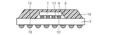
本発明者は、接続信頼性の高い半田合金の組成を得るための実験を行なった。図1は本発明の実施の形態に係る半導体装置を示す図であり、実験では、この構成の半導体装置について、温度変化の繰返しに対する耐久試験(温度サイクル試験)が行われた。以下、その実験について説明する。 The inventor conducted an experiment to obtain a solder alloy composition having high connection reliability. FIG. 1 is a diagram showing a semiconductor device according to an embodiment of the present invention. In an experiment, an endurance test (temperature cycle test) against repeated temperature changes was performed on the semiconductor device having this configuration. Hereinafter, the experiment will be described.
まず、図1の半導体装置の構成について説明する。当該半導体装置は、ボールグリッドアレイ構造により構成されており、半導体チップ1と、半導体チップ1を実装する基板(パッケージ基板)2とを備えている。半導体チップ1は、フェイスダウン方式によりパッケージ基板2に装着されており、集積回路面を当該パッケージ基板2に向けて搭載される。即ち、半導体チップ1の集積回路面に形成された内部電極9と、パッケージ基板2の上面に形成されたボンディングパッド10とが、半田バンプ11を介して電気的且つ機械的に接続される。 First, the configuration of the semiconductor device in FIG. 1 will be described. The semiconductor device has a ball grid array structure, and includes a
上で述べたように、半導体チップ1の電極の狭ピッチ化が進むと、従来の半田バンプでは、充分な接続信頼性を得ることが困難になる。また通常、半導体装置内部の半導体チップ1とパッケージ基板2の間には比較的大きな応力がかかるので、当該半導体チップ1とパッケージ基板2との間の半田バンプ11は、特に高い接続信頼性を得ることができるものである必要性が高い。 As described above, when the pitch of the electrodes of the
半導体チップ1とパッケージ基板2との間隙には、アンダーフィル樹脂3が設けられている。アンダーフィル樹脂3によって、半田バンプ11の接合部分にかかる外部からの応力を緩和させることができ、半導体チップ1とパッケージ基板2との接続信頼を高めている。パッケージ基板2上面には、スティフナー(補強材)4が接着テープ5を介して設けられている。スティフナー4は、応力の発生を抑制するためにパッケージ基板2と線膨張率が近いものが望ましく、例えば銅で構成される。また接着テープ5は、例えば接着性の高いエポキシ系の樹脂により形成される。 An
さらに、半導体装置の放熱性向上と半導体チップ1の保護を目的として、ヒートスプレッダ7が放熱樹脂8を介して半導体チップ1上に搭載される。ヒートスプレッダ7は接着テープ6を介してスティフナー4にも固定される。接着テープ6は、例えば接着性の高いエポキシ系の樹脂により形成される。放熱樹脂8は、ヒートスプレッダ7と半導体チップ1とが熱的に接続するよう、例えば熱伝導性の高い銀ペーストにより形成される。 Furthermore, a heat spreader 7 is mounted on the
そして、パッケージ基板2の裏面においては、複数個の外部電極12が配置されており、この複数個の外部電極12のそれぞれには、この半導体装置をマザーボード等に実装させるための半田ボール13が形成されている。 A plurality of
実験では、図1の構成を有する半導体装置のサンプルについて、半田バンプ11の組成を変化させて、温度サイクル試験を行なった。熱サイクル試験としては、半導体装置単体での試験と、半導体装置をマザーボード基板に実装した状態での試験を行なった。また、半田バンプ11は、Ag,Cu、Snから成る鉛フリー半田を使用した。 In the experiment, a temperature cycle test was performed on a sample of the semiconductor device having the configuration of FIG. 1 by changing the composition of the
その結果、半田バンプ11として、Ag:0〜1.0質量%、Cu:0.2〜1.0質量%を含み、残部はSnから成る半田合金を使用した場合に、特に良好な結果が得られた。具体的には、半導体装置単体での温度サイクル試験において、低温−55℃、高温125℃のサイクルを1000サイクル経ても、この組成の半田バンプ11を有する半導体装置では、全サンプルについて当該半田バンプ11における接続不良は生じなかった。また、半導体装置単体をマザーボード基板に実装した状態での温度サイクル試験では、低温0℃、高温100℃のサイクルを5000サイクル経ても、この組成の半田バンプ11を有する半導体装置では、全サンプルについて半田バンプ11における接続不良は生じなかった。なお、「Ag:0質量%」とは、Agを含んでいない(CuとSnのみから成る)ことを指している。 As a result, when the
つまり、上記実験により、Ag:0〜1.0質量%、Cu:0.2〜1.0質量%を含み、残部はSnから成る半田合金を半田バンプとして使用することによって、高い接続信頼性が得られることが分かった。即ち、図1に示す半導体装置において、半田バンプ11として、この組成の鉛フリー半田を使用すると半導体装置の動作信頼性が向上する。 That is, according to the above experiment, high connection reliability is obtained by using a solder alloy containing Sn: 0 to 1.0 mass%, Cu: 0.2 to 1.0 mass%, with the balance being Sn. Was found to be obtained. That is, when the lead-free solder having this composition is used as the
半田ボール13に関しては、一般的に、外部電極12のピッチは半田バンプ11よりも広いので半田ボール13の堆積を確保することが可能であり、また半導体装置の実装時に半田ボール13にかかる応力は比較的小さいので、従来の半田合金(例えばAg:3〜4質量%、Cu:0.5〜1.0質量%、残部Sn)を使用しても充分な接続信頼性を得ることができる。もちろん、さらに高い接続信頼性を得る目的で、半田バンプ11と同様にAg:0〜1.0質量%、Cu:0.2〜1.0質量%を含み、残部はSnから成る半田合金を使用してもよい。 Regarding the
なお、本実施の形態においては、図1のようにスティフナー4およびヒートスプレッダ7を有する半導体装置について説明したが、本発明の適用はこの構成に限定されるものではない。例えば、図1の構成に対し、ヒートスプレッダ7を有しないタイプ(図2)、スティフナー4を有しないタイプ(図3)、スティフナー4およびヒートスプレッダ7を有しないタイプ(図4)、スティフナー4およびヒートスプレッダ7に代えて上面をモールド樹脂14で覆ったタイプ(図5)の半導体装置に対しても適用可能である。その場合にも、本発明に係るAg:0〜1.0質量%、Cu:0.2〜1.0質量%、残部はSnの半田合金による半田バンプ11および半田ボール13を使用することにより高い接続信頼性が得られる。 In the present embodiment, the semiconductor device having the stiffener 4 and the heat spreader 7 as shown in FIG. 1 has been described. However, the application of the present invention is not limited to this configuration. For example, the type having no heat spreader 7 (FIG. 2), the type not having the stiffener 4 (FIG. 3), the type not having the stiffener 4 and the heat spreader 7 (FIG. 4), the stiffener 4 and the heat spreader 7 in the configuration of FIG. Instead, the present invention can also be applied to a semiconductor device of the type (FIG. 5) whose upper surface is covered with the
1 半導体チップ、2 パッケージ基板、3 アンダーフィル樹脂、4 スティフナー、5,6 接着テープ、7 ヒートスプレッダ、8 放熱樹脂、9 内部電極、10 ボンディングパッド、11 半田バンプ、12 外部電極、13 半田ボール、14 モールド樹脂。
DESCRIPTION OF
Claims (4)
Translated fromJapanese残部はSnから成る半田合金。Ag: 1.0 mass% or less, Cu: 0.2-1.0 mass% included,
The balance is a solder alloy made of Sn.
残部はSnから成る半田合金。Cu: 0.2-1.0 mass% is included,
The balance is a solder alloy made of Sn.
残部はSnから成る半田合金で形成されたバンプを備える半導体装置。Ag: 1.0 mass% or less, Cu: 0.2-1.0 mass% included,
A semiconductor device comprising a bump formed of a solder alloy made of Sn.
残部はSnから成る半田合金で形成されたバンプを備える半導体装置。
Cu: 0.2-1.0 mass% is included,
A semiconductor device comprising a bump formed of a solder alloy made of Sn.
Priority Applications (2)
| Application Number | Priority Date | Filing Date | Title |
|---|---|---|---|
| JP2004022598AJP2005211946A (en) | 2004-01-30 | 2004-01-30 | Solder alloy and semiconductor device |
| US11/029,368US20050167827A1 (en) | 2004-01-30 | 2005-01-06 | Solder alloy and semiconductor device |
Applications Claiming Priority (1)
| Application Number | Priority Date | Filing Date | Title |
|---|---|---|---|
| JP2004022598AJP2005211946A (en) | 2004-01-30 | 2004-01-30 | Solder alloy and semiconductor device |
Publications (1)
| Publication Number | Publication Date |
|---|---|
| JP2005211946Atrue JP2005211946A (en) | 2005-08-11 |
Family
ID=34805669
Family Applications (1)
| Application Number | Title | Priority Date | Filing Date |
|---|---|---|---|
| JP2004022598APendingJP2005211946A (en) | 2004-01-30 | 2004-01-30 | Solder alloy and semiconductor device |
Country Status (2)
| Country | Link |
|---|---|
| US (1) | US20050167827A1 (en) |
| JP (1) | JP2005211946A (en) |
Families Citing this family (3)
| Publication number | Priority date | Publication date | Assignee | Title |
|---|---|---|---|---|
| US7759793B2 (en)* | 2004-12-13 | 2010-07-20 | Renesas Technology Corp. | Semiconductor device having elastic solder bump to prevent disconnection |
| JP2006216911A (en)* | 2005-02-07 | 2006-08-17 | Renesas Technology Corp | Semiconductor device and encapsulated semiconductor package |
| US8319339B2 (en)* | 2009-07-10 | 2012-11-27 | Stmicroelectronics (Tours) Sas | Surface-mounted silicon chip |
Family Cites Families (8)
| Publication number | Priority date | Publication date | Assignee | Title |
|---|---|---|---|---|
| KR100398716B1 (en)* | 2000-06-12 | 2003-09-19 | 가부시키가이샤 히타치세이사쿠쇼 | Semiconductor module and circuit substrate |
| JP4068801B2 (en)* | 2000-11-30 | 2008-03-26 | 株式会社ルネサステクノロジ | Semiconductor device |
| JP2002368168A (en)* | 2001-06-13 | 2002-12-20 | Hitachi Ltd | Composite member for semiconductor device, insulated semiconductor device using the same, or non-insulated semiconductor device |
| JP4105409B2 (en)* | 2001-06-22 | 2008-06-25 | 株式会社ルネサステクノロジ | Multi-chip module manufacturing method |
| JP3897596B2 (en)* | 2002-01-07 | 2007-03-28 | 日本テキサス・インスツルメンツ株式会社 | Mounted body of semiconductor device and wiring board |
| US6767765B2 (en)* | 2002-03-27 | 2004-07-27 | Intel Corporation | Methods and apparatus for disposing a thermal interface material between a heat source and a heat dissipation device |
| US6917113B2 (en)* | 2003-04-24 | 2005-07-12 | International Business Machines Corporatiion | Lead-free alloys for column/ball grid arrays, organic interposers and passive component assembly |
| US20040258556A1 (en)* | 2003-06-19 | 2004-12-23 | Nokia Corporation | Lead-free solder alloys and methods of making same |
- 2004
- 2004-01-30JPJP2004022598Apatent/JP2005211946A/enactivePending
- 2005
- 2005-01-06USUS11/029,368patent/US20050167827A1/ennot_activeAbandoned
Also Published As
| Publication number | Publication date |
|---|---|
| US20050167827A1 (en) | 2005-08-04 |
Similar Documents
| Publication | Publication Date | Title |
|---|---|---|
| JP4731495B2 (en) | Semiconductor device | |
| KR100442695B1 (en) | Method for manufacturing flip chip package devices with heat spreaders | |
| JP2005150478A (en) | Multi-chip module | |
| JP2008166440A (en) | Semiconductor device | |
| JP4828164B2 (en) | Interposer and semiconductor device | |
| WO2006072032A2 (en) | Flip chip contact(pcc) power package | |
| JP3724954B2 (en) | Electronic device and semiconductor package | |
| JP2008135627A (en) | Semiconductor device | |
| JP2006066693A (en) | Semiconductor device | |
| JP2004179442A (en) | Multichip module | |
| TWI242866B (en) | Process of forming lead-free bumps on electronic component | |
| US20070023910A1 (en) | Dual BGA alloy structure for improved board-level reliability performance | |
| US20080164604A1 (en) | Heat dissipating semiconductor package | |
| JP2009302539A (en) | Processing method for low profile solder grid array, device, and computer system | |
| CN101241891B (en) | Semiconductor device and manufacturing method thereof | |
| US20070216003A1 (en) | Semiconductor package with enhancing layer and method for manufacturing the same | |
| KR20090098076A (en) | Flip chip package | |
| JP2005211946A (en) | Solder alloy and semiconductor device | |
| JP2007142097A (en) | Semiconductor device | |
| JP2008098285A (en) | Semiconductor device | |
| JP2024055042A (en) | Semiconductor Device | |
| JP5099714B2 (en) | Multi-chip module | |
| JP5267540B2 (en) | Semiconductor device | |
| JP2008112878A (en) | Semiconductor device | |
| US20120292756A1 (en) | Semiconductor device with heat spreader |