JP2005204493A - Semiconductor device and driving method therefor - Google Patents
Semiconductor device and driving method thereforDownload PDFInfo
- Publication number
- JP2005204493A JP2005204493AJP2004345439AJP2004345439AJP2005204493AJP 2005204493 AJP2005204493 AJP 2005204493AJP 2004345439 AJP2004345439 AJP 2004345439AJP 2004345439 AJP2004345439 AJP 2004345439AJP 2005204493 AJP2005204493 AJP 2005204493A
- Authority
- JP
- Japan
- Prior art keywords
- circuit
- voltage
- antenna
- conversion circuit
- film
- Prior art date
- Legal status (The legal status is an assumption and is not a legal conclusion. Google has not performed a legal analysis and makes no representation as to the accuracy of the status listed.)
- Granted
Links
- 239000004065semiconductorSubstances0.000titleclaimsdescription80
- 238000000034methodMethods0.000titleclaimsdescription65
- 239000000758substrateSubstances0.000claimsdescription89
- 238000006243chemical reactionMethods0.000claimsdescription53
- 239000003990capacitorSubstances0.000claimsdescription44
- 230000002238attenuated effectEffects0.000claimsdescription9
- 239000011521glassSubstances0.000claimsdescription8
- 239000004033plasticSubstances0.000claimsdescription4
- 239000012212insulatorSubstances0.000claimsdescription2
- 239000010409thin filmSubstances0.000claimsdescription2
- 238000010438heat treatmentMethods0.000abstractdescription12
- 230000005672electromagnetic fieldEffects0.000abstractdescription11
- 230000007423decreaseEffects0.000abstractdescription5
- 239000010408filmSubstances0.000description139
- 239000010410layerSubstances0.000description118
- 239000012535impuritySubstances0.000description44
- XUIMIQQOPSSXEZ-UHFFFAOYSA-NSiliconChemical compound[Si]XUIMIQQOPSSXEZ-UHFFFAOYSA-N0.000description29
- 238000005530etchingMethods0.000description29
- 229910052710siliconInorganic materials0.000description29
- 239000010703siliconSubstances0.000description29
- VYPSYNLAJGMNEJ-UHFFFAOYSA-NSilicium dioxideChemical compoundO=[Si]=OVYPSYNLAJGMNEJ-UHFFFAOYSA-N0.000description22
- 229910052814silicon oxideInorganic materials0.000description19
- 239000000853adhesiveSubstances0.000description15
- 239000000463materialSubstances0.000description15
- 239000011229interlayerSubstances0.000description14
- 230000008569processEffects0.000description14
- 230000001070adhesive effectEffects0.000description13
- 239000007789gasSubstances0.000description13
- 238000002425crystallisationMethods0.000description11
- 150000002221fluorineChemical class0.000description11
- 238000004519manufacturing processMethods0.000description11
- 229910044991metal oxideInorganic materials0.000description10
- 150000004706metal oxidesChemical class0.000description10
- 10210003628525-hydroxyvitamin D-1 alpha hydroxylase, mitochondrialHuman genes0.000description8
- 101000875403Homo sapiens 25-hydroxyvitamin D-1 alpha hydroxylase, mitochondrialProteins0.000description8
- 229910052581Si3N4Inorganic materials0.000description8
- 239000000460chlorineSubstances0.000description8
- 230000008025crystallizationEffects0.000description8
- 229910052731fluorineInorganic materials0.000description8
- 239000000047productSubstances0.000description8
- HQVNEWCFYHHQES-UHFFFAOYSA-Nsilicon nitrideChemical compoundN12[Si]34N5[Si]62N3[Si]51N64HQVNEWCFYHHQES-UHFFFAOYSA-N0.000description8
- 239000011737fluorineSubstances0.000description7
- 230000006870functionEffects0.000description7
- 239000011241protective layerSubstances0.000description7
- 229920005989resinPolymers0.000description7
- 239000011347resinSubstances0.000description7
- UFHFLCQGNIYNRP-UHFFFAOYSA-NHydrogenChemical compound[H][H]UFHFLCQGNIYNRP-UHFFFAOYSA-N0.000description6
- 230000006378damageEffects0.000description6
- 239000001257hydrogenSubstances0.000description6
- 229910052739hydrogenInorganic materials0.000description6
- 239000007788liquidSubstances0.000description6
- OAICVXFJPJFONN-UHFFFAOYSA-NPhosphorusChemical compound[P]OAICVXFJPJFONN-UHFFFAOYSA-N0.000description5
- 150000002500ionsChemical class0.000description5
- 229910052698phosphorusInorganic materials0.000description5
- 239000011574phosphorusSubstances0.000description5
- 230000001681protective effectEffects0.000description5
- 238000012546transferMethods0.000description5
- YCKRFDGAMUMZLT-UHFFFAOYSA-NFluorine atomChemical compound[F]YCKRFDGAMUMZLT-UHFFFAOYSA-N0.000description4
- 239000000956alloySubstances0.000description4
- 229910021417amorphous siliconInorganic materials0.000description4
- 238000000137annealingMethods0.000description4
- 125000004429atomChemical group0.000description4
- QVGXLLKOCUKJST-UHFFFAOYSA-Natomic oxygenChemical compound[O]QVGXLLKOCUKJST-UHFFFAOYSA-N0.000description4
- 238000009826distributionMethods0.000description4
- 229910052751metalInorganic materials0.000description4
- 239000002184metalSubstances0.000description4
- 230000010355oscillationEffects0.000description4
- 229910052760oxygenInorganic materials0.000description4
- 239000001301oxygenSubstances0.000description4
- 238000005268plasma chemical vapour depositionMethods0.000description4
- 230000004044responseEffects0.000description4
- 238000004544sputter depositionMethods0.000description4
- 125000001424substituent groupChemical group0.000description4
- MZLGASXMSKOWSE-UHFFFAOYSA-Ntantalum nitrideChemical compound[Ta]#NMZLGASXMSKOWSE-UHFFFAOYSA-N0.000description4
- 229910004298SiO 2Inorganic materials0.000description3
- 230000001133accelerationEffects0.000description3
- 229910045601alloyInorganic materials0.000description3
- -1fluorine halideChemical class0.000description3
- 229910010272inorganic materialInorganic materials0.000description3
- 239000011147inorganic materialSubstances0.000description3
- 239000011810insulating materialSubstances0.000description3
- 229910021421monocrystalline siliconInorganic materials0.000description3
- 238000002360preparation methodMethods0.000description3
- 239000010453quartzSubstances0.000description3
- 239000002356single layerSubstances0.000description3
- 239000010935stainless steelSubstances0.000description3
- 229910001220stainless steelInorganic materials0.000description3
- IJGRMHOSHXDMSA-UHFFFAOYSA-NAtomic nitrogenChemical compoundN#NIJGRMHOSHXDMSA-UHFFFAOYSA-N0.000description2
- ZAMOUSCENKQFHK-UHFFFAOYSA-NChlorine atomChemical compound[Cl]ZAMOUSCENKQFHK-UHFFFAOYSA-N0.000description2
- KRHYYFGTRYWZRS-UHFFFAOYSA-MFluoride anionChemical compound[F-]KRHYYFGTRYWZRS-UHFFFAOYSA-M0.000description2
- 229910000577Silicon-germaniumInorganic materials0.000description2
- BOTDANWDWHJENH-UHFFFAOYSA-NTetraethyl orthosilicateChemical compoundCCO[Si](OCC)(OCC)OCCBOTDANWDWHJENH-UHFFFAOYSA-N0.000description2
- 125000000217alkyl groupChemical group0.000description2
- 150000004945aromatic hydrocarbonsChemical class0.000description2
- 238000005452bendingMethods0.000description2
- 229910052801chlorineInorganic materials0.000description2
- 239000013078crystalSubstances0.000description2
- 238000001514detection methodMethods0.000description2
- 239000010432diamondSubstances0.000description2
- 229910003460diamondInorganic materials0.000description2
- KPUWHANPEXNPJT-UHFFFAOYSA-NdisiloxaneChemical class[SiH3]O[SiH3]KPUWHANPEXNPJT-UHFFFAOYSA-N0.000description2
- 238000001312dry etchingMethods0.000description2
- 238000009499grossingMethods0.000description2
- 238000005984hydrogenation reactionMethods0.000description2
- 238000009616inductively coupled plasmaMethods0.000description2
- 238000005499laser crystallizationMethods0.000description2
- 239000000203mixtureSubstances0.000description2
- 238000012544monitoring processMethods0.000description2
- 238000000206photolithographyMethods0.000description2
- 229910021420polycrystalline siliconInorganic materials0.000description2
- 238000012545processingMethods0.000description2
- 238000000926separation methodMethods0.000description2
- 229910052715tantalumInorganic materials0.000description2
- JOHWNGGYGAVMGU-UHFFFAOYSA-NtrifluorochlorineChemical compoundFCl(F)FJOHWNGGYGAVMGU-UHFFFAOYSA-N0.000description2
- 229910052721tungstenInorganic materials0.000description2
- 238000007740vapor depositionMethods0.000description2
- 238000001039wet etchingMethods0.000description2
- 229910004529TaF 5Inorganic materials0.000description1
- ATJFFYVFTNAWJD-UHFFFAOYSA-NTinChemical compound[Sn]ATJFFYVFTNAWJD-UHFFFAOYSA-N0.000description1
- LEVVHYCKPQWKOP-UHFFFAOYSA-N[Si].[Ge]Chemical compound[Si].[Ge]LEVVHYCKPQWKOP-UHFFFAOYSA-N0.000description1
- 239000006061abrasive grainSubstances0.000description1
- NIXOWILDQLNWCW-UHFFFAOYSA-Nacrylic acid groupChemical groupC(C=C)(=O)ONIXOWILDQLNWCW-UHFFFAOYSA-N0.000description1
- 230000003213activating effectEffects0.000description1
- 230000004913activationEffects0.000description1
- 229910052782aluminiumInorganic materials0.000description1
- PNEYBMLMFCGWSK-UHFFFAOYSA-Naluminium oxideInorganic materials[O-2].[O-2].[O-2].[Al+3].[Al+3]PNEYBMLMFCGWSK-UHFFFAOYSA-N0.000description1
- 239000005407aluminoborosilicate glassSubstances0.000description1
- 229910052785arsenicInorganic materials0.000description1
- RQNWIZPPADIBDY-UHFFFAOYSA-Narsenic atomChemical compound[As]RQNWIZPPADIBDY-UHFFFAOYSA-N0.000description1
- 239000012298atmosphereSubstances0.000description1
- 229910052788bariumInorganic materials0.000description1
- DSAJWYNOEDNPEQ-UHFFFAOYSA-Nbarium atomChemical compound[Ba]DSAJWYNOEDNPEQ-UHFFFAOYSA-N0.000description1
- 230000015572biosynthetic processEffects0.000description1
- 238000009835boilingMethods0.000description1
- 239000005388borosilicate glassSubstances0.000description1
- 229910002091carbon monoxideInorganic materials0.000description1
- 230000003197catalytic effectEffects0.000description1
- 239000000919ceramicSubstances0.000description1
- 230000008859changeEffects0.000description1
- 239000007795chemical reaction productSubstances0.000description1
- 150000001805chlorine compoundsChemical class0.000description1
- 238000000576coating methodMethods0.000description1
- 150000001875compoundsChemical class0.000description1
- 229910052802copperInorganic materials0.000description1
- 238000011161developmentMethods0.000description1
- 238000009792diffusion processMethods0.000description1
- 238000010017direct printingMethods0.000description1
- 238000007599dischargingMethods0.000description1
- 230000000694effectsEffects0.000description1
- 238000005516engineering processMethods0.000description1
- 238000007667floatingMethods0.000description1
- 150000002222fluorine compoundsChemical class0.000description1
- 230000020169heat generationEffects0.000description1
- 229920006015heat resistant resinPolymers0.000description1
- 239000011261inert gasSubstances0.000description1
- 238000005468ion implantationMethods0.000description1
- 238000005224laser annealingMethods0.000description1
- 238000004518low pressure chemical vapour depositionMethods0.000description1
- 238000005259measurementMethods0.000description1
- 230000007246mechanismEffects0.000description1
- 238000001465metallisationMethods0.000description1
- 229910021424microcrystalline siliconInorganic materials0.000description1
- 229910052750molybdenumInorganic materials0.000description1
- 229910052757nitrogenInorganic materials0.000description1
- 239000012299nitrogen atmosphereSubstances0.000description1
- QGLKJKCYBOYXKC-UHFFFAOYSA-NnonaoxidotritungstenChemical compoundO=[W]1(=O)O[W](=O)(=O)O[W](=O)(=O)O1QGLKJKCYBOYXKC-UHFFFAOYSA-N0.000description1
- 238000007645offset printingMethods0.000description1
- 230000003287optical effectEffects0.000description1
- 230000003647oxidationEffects0.000description1
- 238000007254oxidation reactionMethods0.000description1
- 230000001590oxidative effectEffects0.000description1
- 238000000053physical methodMethods0.000description1
- 238000007639printingMethods0.000description1
- 238000004151rapid thermal annealingMethods0.000description1
- 230000009467reductionEffects0.000description1
- 238000007650screen-printingMethods0.000description1
- 239000003566sealing materialSubstances0.000description1
- 239000000126substanceSubstances0.000description1
- 238000002230thermal chemical vapour depositionMethods0.000description1
- 229910052719titaniumInorganic materials0.000description1
- NXHILIPIEUBEPD-UHFFFAOYSA-Htungsten hexafluorideChemical compoundF[W](F)(F)(F)(F)FNXHILIPIEUBEPD-UHFFFAOYSA-H0.000description1
- 229910001930tungsten oxideInorganic materials0.000description1
Images


Landscapes
- Thin Film Transistor (AREA)
- Recrystallisation Techniques (AREA)
- Metal-Oxide And Bipolar Metal-Oxide Semiconductor Integrated Circuits (AREA)
Abstract
Description
Translated fromJapanese本発明はICカードおよびRFID (Radio Frequency IDentification:無線周波数による非接触自動識別技術)に用いる半導体装置に関し、特に非接触で外部機器から電力供給および情報を受け、該外部機器へ情報を送出する非接触ICカードおよびRFIDチップを含む半導体装置およびその駆動方法に関する。 The present invention relates to an IC card and a semiconductor device used for RFID (Radio Frequency IDentification: wireless contactless automatic identification technology by radio frequency), and more particularly, a non-contact device that receives power supply and information from an external device and sends information to the external device. The present invention relates to a semiconductor device including a contact IC card and an RFID chip and a driving method thereof.
なお、RFIDチップは例えば、タグとして用いられる。ICカードはRFIDチップの一種である。 The RFID chip is used as a tag, for example. An IC card is a kind of RFID chip.
近年、ICチップとして無線周波数による非接触なIDチップ、すなわちRFIDチップと呼ばれているものが注目され、高性能化への期待が高まってきている。RFIDチップは非接触で記録情報が読み取れ、無電池で動作し、耐久性、耐候性に優れるなどの特徴を有する。 In recent years, non-contact ID chips using radio frequencies, that is, RFID chips, have attracted attention as IC chips, and expectations for higher performance are increasing. An RFID chip has features such as non-contact reading of recorded information, operation with no battery, and excellent durability and weather resistance.
また、RFIDチップにはCPUなどのコンピュータ回路を組み込むこともでき、情報の記録保存の道具としてだけでなく、セキュリティ管理などの論理回路を組み込むと言ったようなこともできる。RFIDチップ を用いた応用分野として、個人認証、商品の識別、位置測定などがある。 Further, a computer circuit such as a CPU can be incorporated in the RFID chip, and it can be said that a logic circuit such as security management is incorporated as well as a tool for recording and storing information. Application fields using RFID chips include personal authentication, product identification, and position measurement.
従来のRFIDチップは図2のような構成を取っていた。図2に示すRFIDチップ217は電源回路214、入出力回路215、アンテナ回路216、論理回路210、増幅器211、クロック生成回路・デコーダ212、メモリ213等を有する。アンテナ回路216は、アンテナ配線201と、アンテナ容量202とを有している。 A conventional RFID chip has a configuration as shown in FIG. The
RFIDチップは独自の電源を持たない代わりに、RFリーダー/ライター200から発せられる電磁波218を受け取ることで電力が供給され動作する。 The RFID chip does not have its own power source, but operates by being supplied with electric power by receiving the
RFIDチップ217の動作を図2を用いて説明する。RFリーダー/ライター200からの電磁波218をアンテナ回路216が受け取ると、第1の容量手段203、第1のダイオード204及び第3のダイオード207、第3の容量手段208等によって構成される入出力回路215により、検波出力信号として検出される。この信号は増幅器211によって十分大きな振幅に増幅された後、クロック生成回路・デコーダ212によってクロックとデータ・命令に分離され、送られた命令を論理回路210で解読し、メモリ213内のデータの返答、必要事項のメモリへの書き込み等を行う。 The operation of the
データの返答は論理回路210の出力によってスイッチング素子209をオン/オフすることによって行う。これによってアンテナ回路216のインピーダンスが変化して結果としてアンテナ回路216の反射率を変化させる。RFリーダー/ライター200はアンテナ回路216の反射率の変化をモニターすることで、RFIDチップ217からの情報を読み取る。 Data is returned by turning on / off the
RFIDチップ217内の各回路で消費する電力は電源回路214において、アンテナ216で受信した電磁波218を検波、平滑することで生じる直流電源VDDによって供給される。電源回路214は、第1の容量手段203、第1のダイオード204、第2のダイオード205、第2の容量手段206によって構成されるが、第2の容量手段206は各回路に電力を供給するために十分大きな値を設定している。 The power consumed by each circuit in the
図11はアンテナ回路216が受信したアンテナ入力信号(A)に対する電源回路214から出力される直流電源の出力(B)を示したものである。アンテナ入力信号は第1のダイオード204および第2のダイオード205によって負成分は取り除かれ、正成分のみが第2のダイオード205を通過して各回路に供給される。容量手段206は第2のダイオード205を通過した正成分を蓄え、アンテナ入力信号が負のときに電力を供給する。したがってVDDはおおむね一定値となり、電源回路214は直流電圧源としての働きを持つ。 FIG. 11 shows the output (B) of the DC power supply output from the
このような回路の例として、例えば下記特許文献1がある。
図3は、RFIDチップ309に使われる回路のうち、アンテナ回路308と電源回路307を抜き出したものである。アンテナ回路308は、アンテナ配線301と、アンテナ容量302とを有している。また電源回路307は、第1の容量手段303と、第1のダイオード304と、第2のダイオード305と、第2の容量手段306とを有している。 FIG. 3 shows an
RFIDチップは無電池で動作することを特徴のひとつとして挙げられるが、前述したようにRFIDリーダー/ライターから発せられる電磁界をアンテナ回路308で取りこみ、電源回路307で整流することにより発生する直流電圧によって、RFIDチップ内に組み込まれた回路が作動する仕組みになっている。 One of the features of the RFID chip is that it operates without a battery. As described above, the DC voltage generated by capturing the electromagnetic field generated from the RFID reader / writer by the
図12に、アンテナ回路308が受信した電磁界の強度(実効値)に対する電源回路307が整流した直流電圧の強度の関係を示す。図12に示すように、電源回路307が整流した直流電圧の強度は元の電磁界の強度におおむね比例して決まる。したがって、アンテナ回路308が強電磁界にさらされた場合にはアンテナ回路308内部で高電圧交流信号が発生し、その結果電源回路307で行われる交流電圧の整流によって得られた直流電圧もまた高電圧となる。 FIG. 12 shows the relationship between the strength (effective value) of the electromagnetic field received by the
このことにより論理回路部内のメモリ、クロック生成回路などに高電圧が印加され、論理回路部が発熱する、もしくは回路に用いられる素子が高電圧によって破壊されるなどの不具合が発生してしまうという問題があった。 This causes a problem that a high voltage is applied to the memory, clock generation circuit, etc. in the logic circuit section, and the logic circuit section generates heat, or an element used in the circuit is destroyed by the high voltage. was there.
上記問題に鑑み、本発明では強電磁界に置かれた場合においても高電圧の発生を防ぎ、以って回路の加熱、素子の破損を防ぐことを課題とする。 In view of the above problems, an object of the present invention is to prevent generation of a high voltage even when placed in a strong electromagnetic field, thereby preventing circuit heating and element damage.
上記課題を解決するために、本発明では、電源回路に出力される直流電圧をモニターし、参照電圧との比較を行なう。そして、モニターされた直流電圧が前記参照電圧を超えたときに、容量手段をアンテナ回路内のアンテナ配線と並列に接続して、アンテナ回路における交流電圧の共振点を変化させ、前記交流電圧を減衰させることを特徴とする。上記構成により、電源回路に出力される直流電圧値を下げることができる。 In order to solve the above problems, in the present invention, the DC voltage output to the power supply circuit is monitored and compared with the reference voltage. When the monitored DC voltage exceeds the reference voltage, the capacitive means is connected in parallel with the antenna wiring in the antenna circuit, the resonance point of the AC voltage in the antenna circuit is changed, and the AC voltage is attenuated. It is characterized by making it. With the above configuration, the DC voltage value output to the power supply circuit can be lowered.
本発明は、交流電圧を整流して直流電圧に変換する変換回路と、論理回路と、メモリと、入出力回路とを有する半導体装置において、入出力回路および変換回路にはアンテナ回路が電気的に接続され、参照電圧源と、参照電圧源の出力電圧と変換回路の出力電圧とを比較する比較回路と、比較回路によって制御され、一端が接地されたスイッチング素子と、一端がアンテナ回路に電気的に接続され、他端がスイッチング素子の接地されていない端に電気的に接続された容量手段とを、有することを特徴とする。 The present invention relates to a semiconductor device having a conversion circuit that rectifies and converts an AC voltage into a DC voltage, a logic circuit, a memory, and an input / output circuit. An antenna circuit is electrically connected to the input / output circuit and the conversion circuit. A reference voltage source, a comparison circuit for comparing the output voltage of the reference voltage source and the output voltage of the conversion circuit, a switching element controlled by the comparison circuit and having one end grounded, and one end electrically connected to the antenna circuit And capacitive means electrically connected to the other end of the switching element that is not grounded.
また本発明は、交流電圧を整流して直流電圧に変換する変換回路と、論理回路と、メモリと、入出力回路とを有する半導体装置において、入出力回路および変換回路にはアンテナ回路が電気的に接続され、複数の参照電圧源と、複数の参照電圧源の出力電圧と変換回路の出力電圧とを比較する複数の比較回路と、複数の比較回路によって制御され、一端が接地された複数のスイッチング素子と、一端がアンテナ回路に電気的に接続され、他端が複数のスイッチング素子の接地されていない端に電気的に接続された複数の容量手段とを、有することを特徴とする。 The present invention also provides a semiconductor device having a conversion circuit that rectifies and converts an AC voltage into a DC voltage, a logic circuit, a memory, and an input / output circuit. An antenna circuit is electrically connected to the input / output circuit and the conversion circuit. A plurality of reference voltage sources, a plurality of comparison circuits for comparing the output voltages of the plurality of reference voltage sources and the output voltage of the conversion circuit, and a plurality of comparison circuits controlled by the plurality of comparison circuits and having one end grounded It has a switching element and a plurality of capacitive means having one end electrically connected to the antenna circuit and the other end electrically connected to the ungrounded ends of the plurality of switching elements.
また本発明は、交流電圧を整流して直流電圧に変換する変換回路と、論理回路と、メモリと、入出力回路回路と、比較回路と、参照電圧源と、スイッチング素子と、容量手段とを有する半導体装置の駆動方法において、入出力回路および変換回路にはアンテナ回路が電気的に接続され、変換回路の出力と、参照電圧源とが比較回路に電気的に接続され、比較回路の出力がスイッチング素子と電気的に接続され、スイッチング素子の一端は接地され、他端は容量手段と電気的に接続され、容量手段のスイッチング素子と接続されていない一端がアンテナ回路に電気的に接続され、比較回路で変換回路によって変換された直流電圧の値と参照電圧の値の比較を行い、直流電圧の値が参照電圧の値を超えたときに、スイッチング素子が動作して、容量手段の一端を接地することによって、アンテナ回路における交流電圧の共振点が変化して交流電圧を減衰させることにより、変換回路の出力電圧を下げることを特徴とする。 The present invention also includes a conversion circuit that rectifies and converts an AC voltage into a DC voltage, a logic circuit, a memory, an input / output circuit circuit, a comparison circuit, a reference voltage source, a switching element, and a capacitor means. In the driving method of the semiconductor device having the antenna circuit, the antenna circuit is electrically connected to the input / output circuit and the conversion circuit, the output of the conversion circuit and the reference voltage source are electrically connected to the comparison circuit, and the output of the comparison circuit is Electrically connected to the switching element, one end of the switching element is grounded, the other end is electrically connected to the capacitive means, and one end not connected to the switching element of the capacitive means is electrically connected to the antenna circuit, The comparison circuit compares the value of the DC voltage converted by the conversion circuit with the value of the reference voltage. When the value of the DC voltage exceeds the value of the reference voltage, the switching element operates to By grounding one end of the unit, by attenuating the alternating voltage changes the resonance point of the AC voltage in the antenna circuit, and wherein the lower the output voltage of the converter circuit.
また本発明は、交流電圧を整流して直流電圧に変換する変換回路と、論理回路と、メモリと、入出力回路と、複数の比較回路と、複数の参照電圧源と、複数のスイッチング素子と、複数の容量手段とを有する半導体装置の駆動方法において、入出力回路および変換回路にはアンテナ回路が電気的に接続され、変換回路の出力と、複数の参照電圧源とが複数の比較回路のそれぞれと電気的に接続され、複数の比較回路の出力がそれぞれ異なる複数のスイッチング素子と電気的に接続され、複数のスイッチング素子の一端は接地され、他端はそれぞれ異なる複数の容量手段と電気的に接続され、複数の容量手段それぞれのスイッチング素子と接続されていない一端がアンテナ回路に電気的に接続され、複数の比較回路のそれぞれで変換回路によって変換された直流電圧の値と複数の参照電圧の値の比較を行い、直流電圧の値が参照電圧の値を超えたときに、複数のスイッチング素子のうち一つまたは複数が動作して、複数の容量手段のうち一つまたは複数のものの一端を接地させることによって、アンテナ回路における交流電圧の共振点が変化して交流電圧を減衰させることにより、変換回路の出力電圧を下げることを特徴とする。 The present invention also provides a conversion circuit that rectifies an AC voltage to convert it to a DC voltage, a logic circuit, a memory, an input / output circuit, a plurality of comparison circuits, a plurality of reference voltage sources, and a plurality of switching elements. In the method of driving a semiconductor device having a plurality of capacitance means, an antenna circuit is electrically connected to the input / output circuit and the conversion circuit, and the output of the conversion circuit and the plurality of reference voltage sources are connected to the plurality of comparison circuits. Each of the switching circuits is electrically connected to a plurality of different switching elements, and one end of each of the plurality of switching elements is grounded and the other end is electrically connected to a plurality of different capacitance means. One end of each of the plurality of capacitive means not connected to the switching element is electrically connected to the antenna circuit, and each of the plurality of comparison circuits is connected by a conversion circuit. The converted DC voltage value is compared with a plurality of reference voltage values, and when the DC voltage value exceeds the reference voltage value, one or more of the plurality of switching elements operate, The output voltage of the conversion circuit is lowered by attenuating the AC voltage by grounding one end of one or more of the capacitor means to change the resonance point of the AC voltage in the antenna circuit. .
本発明により特殊なプロセスを適用することなく、強電磁界中においても素子の破損を招くことのない半導体装置、およびその駆動方法を実現することができる。また、比較回路を複数設ける構成を取った場合、擬似的に電圧を標準化する標準化回路を提供することが可能である。 According to the present invention, a semiconductor device that does not cause damage to elements even in a strong electromagnetic field and a driving method thereof can be realized without applying a special process. In addition, when a configuration in which a plurality of comparison circuits are provided is provided, it is possible to provide a standardization circuit that standardizes voltages in a pseudo manner.
図4を用いて本発明のRFIDチップ413ついて説明する。図4に示すように本発明では、電源回路に出力されるVDDのモニター回路407、参照電圧源412および直流電圧と参照電圧源412の電圧とを比較する比較回路408、スイッチング素子409、第1の容量手段403を電源回路410に新たに設ける。 The
さらに電源回路410は、第1のダイオード404と、第2のダイオード405と、第2の容量手段406とを有している。第1のダイオード404、第2のダイオード405、第2の容量手段406からなる回路部(変換回路414)は、交流信号を整流して直流信号に変換する機能を有する。また、アンテナ回路411は、アンテナ配線401と、アンテナ容量402とを有している。 Further, the
図4を用いてRFIDチップ413の動作の説明を行う。アンテナ回路411にさらされる電磁界が強くない場合、すなわち発生する直流電圧の値が参照電圧源412の電圧の値を下回るような場合は比較回路408は動作せず、よってスイッチング素子409も動作しない。 The operation of the
アンテナ回路411が強電磁界にさらされることによって直流電圧の値がある一定以上になると比較回路408が作動し、それによってスイッチング素子409がオンして容量手段403の一端が接地される。これはすなわちアンテナ回路411の容量が増大することと等価であり、アンテナ回路411の同調点が最適値より変化することで信号が減衰する。それによって、発生するVDDの電圧値が低下する。よってアンテナ回路411が強電磁界にさらされた場合でもVDDの電圧を抑えることができ、論理回路に高電圧が掛かることを防ぐことができる。このようなアンテナ実装のチップは無線チップとも呼ぶ。 When the
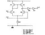
本発明のより具体的な構成について、図1を用いて説明する。図1は、本発明のRFIDチップの一例である。RFIDチップ100は絶縁基板上に形成されたアンテナ回路101、電源回路102、入出力回路103、変換回路123などを有する。 A more specific configuration of the present invention will be described with reference to FIG. FIG. 1 is an example of an RFID chip according to the present invention. The
アンテナ回路101は、アンテナ配線105、アンテナ容量106を有する。電源回路102は、モニター回路104、第1のダイオード107、第2のダイオード108、第1の容量手段109、比較回路112、第1のスイッチング素子113、第2の容量手段114を有する。入出力回路103は第1のダイオード107(電源回路102で用いられているものと共通)、第3のダイオード115、第3の容量手段116、第2のスイッチング素子117、増幅器118、クロック生成回路・デコーダ119、論理回路120、メモリ121、参照電圧源122を有する。変換回路123は、第1のダイオード107、第1のダイオード108、第1の容量手段109を有する。 The
本発明のRFIDチップの動作について、図1を用いて説明する。RFリーダー/ライター(図示せず)からの電磁波をアンテナ回路101が受け取ると、入出力回路103により、検波出力信号として検出される。この信号は増幅器118によって十分大きな振幅に増幅された後、クロック生成回路・デコーダ119によってクロックとデータ・命令に分離され、送られた命令を論理回路120で解読し、メモリ121内のデータの返答、必要事項のメモリへの書き込み等を行う。 The operation of the RFID chip of the present invention will be described with reference to FIG. When the
返答は入出力回路103の出力によって第2のスイッチング素子117をオン/オフすることによって行う。これによってアンテナ回路101のインピーダンスが変化して結果としてアンテナ回路101の反射率を変化させる。RFリーダー/ライターはアンテナ回路101の反射率の変化をモニターすることで、RFIDチップ100からの情報を読み取る。 The response is made by turning on / off the
RFIDチップ内の各回路で消費する電力は電源回路102により受信した電磁波を検波、平滑することで生じる直流電源VDDによって供給される。電源回路102内の変換回路123は、交流電圧を整流して直流電圧に変換する機能を有する。変換回路123は、第1のダイオード107と第2のダイオード108と第1の容量手段109によって構成されるが、第1の容量手段109は各回路に電力を供給するために十分大きな値を設定している。 The power consumed by each circuit in the RFID chip is supplied by a DC power supply VDD generated by detecting and smoothing the electromagnetic wave received by the
直流電源の電圧VDDはRFリーダー/ライターからの電磁波の強度によって決定されるが、このとき電磁波が強すぎることによってVDDが必要以上に高電圧となり、回路の発熱や素子の破壊などの不具合が起きることを防ぐためにモニター回路104、比較回路112、第1のスイッチング素子113、参照電圧源122を用いて直流電圧VDDのコントロールを行う。 The voltage VDD of the DC power supply is determined by the intensity of the electromagnetic wave from the RF reader / writer, but at this time, the electromagnetic wave is too strong, so that VDD becomes higher than necessary, causing problems such as circuit heat generation and element destruction. In order to prevent this, the DC voltage VDD is controlled using the
モニター回路104として、図1では抵抗素子110、抵抗素子111を用いた。比較回路112内でモニター回路104から出力されたVDDと参照電圧源122の電圧との比較を行う。参照電圧源122はどのような構成でも構わないが、RFIDチップの性質上特に回路の面積に制約があると考えられるのでVDDを利用して構成すると好ましい。本実施形態ではVDDを用いて参照電圧を発生させる回路を構成した。 As the
参照電圧源122の構成例を図21に示す。この回路は抵抗素子1701及びダイオード1702〜1704から構成される。ダイオード1702〜1704には例えば、TFT素子をダイオード接続したものを用いることができる。 A configuration example of the
図21において、抵抗素子1701は一端をVDDに接続し、もう一端はOUTPUT(これが図1において参照電圧源122の電圧となる)に接続されている。また、ダイオード1702〜1704は直列に接続され、一端は接地され、もう一端はOUTPUTに接続されている。このような構成によって参照電圧を発生させることができる。このときのOUTPUTとVDDの電圧比は抵抗素子1701によって容易に決定、変更することが可能である。もちろん、この図で挙げた例は一例であって、回路構成、ダイオードの材質及び個数はこれに限定されるものではない事を付記する。 In FIG. 21, one end of the
このように参照電圧源122で発生させた電圧とモニター回路104からの出力電圧を比較回路112で比較し、参照電圧源122で発生させた電圧の方が大きい場合、第1のスイッチング素子は駆動せずにVDDの電圧値はそのまま論理回路120などに掛かる。一方、モニター回路104からの出力電圧が参照電圧源122で発生させた電圧を上回る場合は、比較回路112からの出力によって第1のスイッチング素子113を駆動させることで第2の容量手段114の一端が接地される。これはすなわちアンテナ回路101の容量が増大することと等価であり、アンテナ回路101の同調点が最適値より変化することで信号が減衰する。それによって、発生するVDDの電圧値が低下する。よってアンテナ回路101が強電磁界にさらされた場合でもVDDの電圧を抑えることができ、論理回路120などに高電圧が掛かることを防ぐことができる。 In this way, the voltage generated by the
比較回路112は公知のものを用いることができるが、ここでは比較回路112の一例として、図16にコンパレータ回路を示す。コンパレータ回路はP型TFT601、602、N型TFT603、604、定電流源605、インバータ606、607を有する。コンパレータ回路は2つの入力端子IN1、IN2を有し、IN1はNchTFT603のゲートに接続され、IN2はNchTFT604のゲートと接続される。NchTFT603のドレインもしくはソースのどちらか一端はPchTFT601、602のゲートと、PchTFT601のドレインもしくはソースのどちらか一端と接続される。NchTFT604のドレインもしくはソースのどちらか一端は(この点をA点とする)PchTFT601のドレインもしくはソースのどちらか一端と接続される。またA点は直列に接続されたインバータ606、607と接続されてこの回路の出力となる。そしてNchTFT603、604のもう一端は定電流源605と接続され、PchTFT601、602のもう一端はVDDと接続される。 Although a known circuit can be used as the
コンパレータ回路は2つの入力端子IN1、IN2を有し、両者の信号電圧によって出力が変化する。IN1、IN2ともN型TFT603をオンできない場合、A点は浮遊状態となる。IN1のみがN型TFT603をオンできる場合は、定電流源605はP型TFT601、602に電流を送りP型TFT601、602をオンさせる。従ってA点の電位はHiとなり、出力もまたHiとなる。一方、IN2のみがN型TFT603をオンできる場合はA点に定電流源605からの電流が入りA点の電位はLoとなる。両方ともN型TFT603をオンできる、すなわちIN1はN型TFT603をオンでき、IN2はN型TFT604をオンできる電圧の場合は電圧の高い方が優先される。例えばIN1の電圧がIN2の電圧を上回るとN型TFT603が先にオンして定電流源605はP型TFT601、602に電流を送りP型TFT601、602をオンさせる。従ってA点の電位はHiとなり、出力もまたHiとなる。 The comparator circuit has two input terminals IN1 and IN2, and the output changes depending on the signal voltage of both. When N-
この仕組みを利用して、IN1にモニター回路104からの出力、IN2に参照電圧源122からの電圧信号を入力する。このとき、参照電圧源122の電圧は少なくともN型TFT604をオンできるだけの電圧を持つようにする。このような入力にすることで、参照電圧源122の電圧の方が高いときには比較回路の出力はLoとなり、モニター回路104からの出力が参照電圧源122の電圧よりも高くなった時点で比較回路112の出力はHiとなる。 Using this mechanism, the output from the
もちろんコンパレータ回路の例はこれだけに限定されず、例えば図23に示すような構成をとり、モニター回路104からの出力VDDが大きくなるまではIN1側に入る電圧よりもIN2側に入る電圧が大きくなるようにしてもよい。 Of course, the example of the comparator circuit is not limited to this. For example, the configuration shown in FIG. 23 is adopted, and the voltage entering the IN2 side is larger than the voltage entering the IN1 side until the output VDD from the
図23で示されているコンパレータ回路の構成は、PchTFT1901、1902、NchTFT1903、1904、定電流源1905、インバータ1906、1907、NchTFT1908から構成される。コンパレータ回路は2つの入力端子IN1、IN2を有し、IN1はNchTFT1908のドレインもしくはソースのどちらか一端と接続される。NchTFT1908のもう一端はNchTFT1903のゲートに接続される。IN2はNchTFT1904のゲート及びNchTFT1908のゲートと接続される。NchTFT1903のドレインもしくはソースのどちらか一端はPchTFT1901、1902のゲートと、PchTFT1901のドレインもしくはソースのどちらか一端と接続される。NchTFT1904のドレインもしくはソースのどちらか一端は(この点をA点とする)PchTFT1902のドレインもしくはソースのどちらか一端と接続される。またA点は直列に接続されたインバータ1906、1907と接続されてこの回路の出力となる。そしてNchTFT1903、1904のもう一端は定電流源1905と接続され、PchTFT1901、1902のもう一端はVDDに接続される。図23で示されている回路はIN1の入力がNchTFT1908を通ることによって閾値分の電圧が低下することを利用してIN1側に入る電圧よりもIN2側に入る電圧が大きくなるように構成されていることを特徴とする。 The configuration of the comparator circuit shown in FIG. 23 includes
なお、比較回路112および参照電圧源122は一種類に限定する必要はなく、複数の参照電圧源を用いてもよい。図5においては複数の比較回路および参照電圧源を用いた一例として、3つの比較回路およびそれぞれ異なる参照電圧源を用いた例を示す。 Note that the
モニター回路から出力された直流電圧VDDは、第1の比較回路507、第2の比較回路508、第3の比較回路509において異なる3つの参照電圧源510、511、512からの電圧信号ref1、ref2、ref3とモニター回路からの出力電圧の比較を行う。 The DC voltage VDD output from the monitor circuit is supplied to voltage signals ref1, ref2 from three different
ここで参照電圧源510、511、512からの電圧ref1、ref2、ref3の大きさをref1<ref2<ref3と定めると、モニター回路からの出力がref1を下回る場合はどのスイッチング素子も動作せず、モニター回路からの出力がref1を上回りref2を下回る場合は第1のスイッチング素子504のみが動作して第1の容量手段501の容量が実効的にアンテナ回路に追加される。モニター回路からの出力がref2を上回りref3を下回る場合は第1のスイッチング素子504と第2のスイッチング素子505が動作して第1の容量手段501と第2の容量手段502の容量が実効的にアンテナ回路に追加される。そしてモニター回路からの出力がref3を上回る場合はすべてのスイッチング素子が動作して第1の容量手段501、第2の容量手段502、第3の容量手段503の容量が実効的にアンテナ回路に追加される。 Here, when the magnitudes of the voltages ref1, ref2, and ref3 from the
このように複数の参照電圧源と比較回路を用いた場合、アンテナ回路が受信する電磁波の強度によって段階的に容量を増やすことができるのでより好ましい。電圧参照源の数によっては、出力する電圧を特定の値に擬似的に標準化することも可能である。 Thus, it is more preferable to use a plurality of reference voltage sources and comparison circuits because the capacity can be increased stepwise depending on the intensity of electromagnetic waves received by the antenna circuit. Depending on the number of voltage reference sources, the output voltage can be pseudo-standardized to a specific value.
これらの回路を同一基板上で構成することにより、RFIDチップとしての機能をもつ回路が構成される。なお、RFIDチップ100に用いられる基板は絶縁性をもつものであればどのような材質でも用いることができる。例えばガラス、プラスチック、フィルム状の絶縁体などである。 By configuring these circuits on the same substrate, a circuit having a function as an RFID chip is configured. Note that any material can be used for the substrate used in the
図22を用いて、図1で示した電源回路102と異なる形態の電源回路部について説明する。図22は第1のアンテナ回路1801、第2のアンテナ回路1802、第1の変換回路1803、第2の変換回路1804、比較回路1805スイッチング素子1806、容量手段1807から構成される回路である。第2のアンテナ回路1802は第1のアンテナ回路1801よりも発生する電圧値が低くなるように構成する。例えば、第2のアンテナ回路内部のアンテナの面積を第1のアンテナ回路1802内部で用いられているアンテナの面積よりも小さくする、またはアンテナ回路内部のアンテナまたは容量手段の構成を変更して共振周波数からわずかにずらすというような構成を取ることができる。図示しないが、変換回路と比較回路の間に図1で示されたようなモニター回路を設けてもよい。 A power supply circuit portion having a different form from the
この回路の動作を説明する。第1のアンテナ回路1801で発生された交流電圧は第1の変換回路1803によって整流されて直流電圧VDD1となり、第2のアンテナ回路で発生された交流電圧は第2の変換回路1804によって整流されて直流電圧VDD2となり、比較回路1805に入力される。比較回路1805でVDD1とVDD2の比較をおこない、VDD1の方が大きければ比較回路1805は、Hiを出力してスイッチング素子1806を駆動して第1のアンテナ回路1801に容量手段1807の容量が実効的に追加されてVDD1の電位を低減させる。 The operation of this circuit will be described. The AC voltage generated by the
なお、このような構成をとることにより第1の変換回路で発生される電圧VDD1と第2の変換回路で発生される電圧VDD2の関係は常にVDD1>VDD2が成り立つことになるが、例えば比較回路に図23のような回路を用いることによってVDD1を閾値分低下させる構成を取れば、VDD1とVDD2の差が閾値分になるまで比較回路1805の出力をLoにしてスイッチング素子1806を動作させないようにすることができる。 With this configuration, the relationship between the voltage VDD1 generated by the first conversion circuit and the voltage VDD2 generated by the second conversion circuit always satisfies VDD1> VDD2. For example, the comparison circuit 23, if VDD1 is lowered by a threshold value, the output of the
このような構成を取ることによって、図1で示した例と同様に回路に過大な電圧が掛かることを防ぐことが可能となる。 By adopting such a configuration, it is possible to prevent an excessive voltage from being applied to the circuit as in the example shown in FIG.
本実施例においては、同一の絶縁基板上に実施の形態で示したスイッチング素子及びダイオードに用いるTFTを同時(一体的)に作製する方法について図6乃至図8を用いて説明する。なお、本実施例では半導体素子としてN型TFT、P型TFTを例に挙げて示すが、本発明においてIDチップに含まれる半導体素子はこれに限定されない。また、この作製方法は一例であって、本発明は絶縁基板上での作製方法を限定するものではない。 In this example, a method for manufacturing TFTs used for the switching element and the diode shown in the embodiment mode on the same insulating substrate at the same time (integrated) will be described with reference to FIGS. Note that in this embodiment, an N-type TFT and a P-type TFT are shown as examples of the semiconductor element, but the semiconductor element included in the ID chip in the present invention is not limited to this. This manufacturing method is an example, and the present invention does not limit the manufacturing method over an insulating substrate.
まず、図6(A)に示すように、コーニング社の#7059ガラスや#1737ガラスなどに代表されるバリウムホウケイ酸ガラス、またはアルミノホウケイ酸ガラスなどのガラスから成る、もしくは耐熱性プラスチックからなる基板3000上に酸化シリコン膜、窒化シリコン膜または酸化窒化シリコン膜などの絶縁膜から成る下地膜3001を形成する。例えば、プラズマCVD法でSiH4、NH3、N2Oから作製される酸化窒化シリコン膜3001aを10〜200nm(好ましくは50〜100nm)形成し、同様にSiH4、N2Oから作製される酸化窒化水素化シリコン膜3001bを50〜200nm(好ましくは100〜150nm)の厚さに積層形成する。本実施例では下地膜3001を2層構造として示したが、前記絶縁膜の単層膜または2層以上積層させた構造として形成しても良い。First, as shown in FIG. 6A, a substrate made of glass such as barium borosilicate glass or aluminoborosilicate glass represented by Corning # 7059 glass or # 1737 glass, or made of heat-resistant plastic. A
なお基板3000として、石英基板、セラミック基板等を用いても良い。 Note that a quartz substrate, a ceramic substrate, or the like may be used as the
島状半導体層3002〜3006は、非晶質構造を有する半導体膜をレーザ結晶化法や公知の熱結晶化法を用いて作製した結晶質半導体膜で形成する。この島状半導体層3002〜3006の厚さは25〜80nm(好ましくは30〜60nm)の厚さで形成する。結晶質半導体膜の材料に限定はないが、好ましくはシリコンまたはシリコンゲルマニウム(SiGe)合金などで形成すると良い。 The island-shaped semiconductor layers 3002 to 3006 are formed using a crystalline semiconductor film in which a semiconductor film having an amorphous structure is formed using a laser crystallization method or a known thermal crystallization method. The island-like semiconductor layers 3002 to 3006 are formed with a thickness of 25 to 80 nm (preferably 30 to 60 nm). There is no limitation on the material of the crystalline semiconductor film, but the crystalline semiconductor film is preferably formed of silicon or a silicon germanium (SiGe) alloy.
結晶質半導体膜を用いる場合、まず非晶質半導体を成膜して、公知の結晶化方法を用いて該非晶質半導体を結晶化すれば良い。公知の結晶化方法としては、加熱器による加熱で結晶化を行なう方法、レーザー光の照射で結晶化を行なう方法、触媒金属を用いて結晶化を行なう方法、赤外光を用いて結晶化を行なう方法等が挙げられる。 In the case of using a crystalline semiconductor film, an amorphous semiconductor is first formed, and the amorphous semiconductor may be crystallized using a known crystallization method. Known crystallization methods include crystallization by heating with a heater, crystallization by laser light irradiation, crystallization using a catalytic metal, and crystallization using infrared light. The method of performing etc. are mentioned.
レーザ結晶化法で結晶質半導体膜を作製するには、パルス発振型または連続発光型のエキシマレーザやYAGレーザ、YVO4レーザを用いる。これらのレーザを用いる場合には、レーザ発振器から放射されたレーザ光を光学系で線状に集光し半導体膜に照射する方法を用いると良い。結晶化の条件は実施者が適宣選択するものであるが、エキシマレーザを用いる場合はパルス発振周波数30Hzとし、レーザーエネルギー密度を100〜400mJ/cm2 (代表的には200〜300mJ/cm2)とする。また、YAGレーザを用いる場合にはその第2高調波を用いパルス発振周波数1〜10kHzとし、レーザーエネルギー密度を300〜600mJ/cm2 (代表的には350〜500mJ/cm2)とすると良い。そして幅100〜1000μm、例えば400μmで線状に集光したレーザ光を基板全面に渡って照射し、この時の線状レーザ光の重ね合わせ率(オーバーラップ率)を80〜98%として行う。In order to manufacture a crystalline semiconductor film by a laser crystallization method, a pulse oscillation type or a continuous emission type excimer laser, a YAG laser, or a YVO4 laser is used. In the case of using these lasers, it is preferable to use a method in which laser light emitted from a laser oscillator is linearly collected by an optical system and irradiated onto a semiconductor film. The crystallization conditions are appropriately selected by the practitioner. When an excimer laser is used, the pulse oscillation frequency is 30 Hz, and the laser energy density is 100 to 400 mJ / cm2 (typically 200 to 300 mJ / cm2). ). In the case of using a YAG laser, the second harmonic is used, the pulse oscillation frequency is set to 1 to 10 kHz, and the laser energy density is set to 300 to 600 mJ / cm2 (typically 350 to 500 mJ / cm2 ). Then, a laser beam condensed linearly with a width of 100 to 1000 μm, for example, 400 μm, is irradiated over the entire surface of the substrate, and the superposition ratio (overlap ratio) of the linear laser light at this time is set to 80 to 98%.
また、その発振周波数が10MHz以上のパルス発振のレーザ(MHzLC)を用いて結晶化を行なっても良い。 Further, crystallization may be performed using a pulsed laser (MHzLC) having an oscillation frequency of 10 MHz or more.
次いで、島状半導体層3002〜3006を覆うゲート絶縁膜3007を形成する。ゲート絶縁膜3007はプラズマCVD法またはスパッタ法を用い、厚さを40〜150nmとしてシリコンを含む絶縁膜で形成する。本実施例では、120nmの厚さの酸化窒化シリコン膜で形成する。勿論、ゲート絶縁膜はこのような酸化窒化シリコン膜に限定されるものでなく、他のシリコンを含む絶縁膜を単層または積層構造として用いても良い。例えば、酸化シリコン膜を用いる場合には、プラズマCVD法でTEOS(Tetraethyl Orthosilicate)とO2とを混合し、反応圧力40Pa、基板温度300〜400℃とし、高周波(13.56MHz)、電力密度0.5〜0.8W/cm2で放電させて形成することができる。このようにして作製される酸化シリコン膜は、その後400〜500℃の熱アニールによりゲート絶縁膜として良好な特性を得ることができる。Next, a gate insulating film 3007 is formed to cover the island-shaped semiconductor layers 3002 to 3006. The gate insulating film 3007 is formed of an insulating film containing silicon with a thickness of 40 to 150 nm by a plasma CVD method or a sputtering method. In this embodiment, a silicon oxynitride film having a thickness of 120 nm is formed. Needless to say, the gate insulating film is not limited to such a silicon oxynitride film, and another insulating film containing silicon may be used as a single layer or a stacked structure. For example, when a silicon oxide film is used, TEOS (Tetraethyl Orthosilicate) and O2 are mixed by a plasma CVD method to obtain a reaction pressure of 40 Pa, a substrate temperature of 300 to 400 ° C., a high frequency (13.56 MHz), and a power density of 0. It can be formed by discharging at 5 to 0.8 W / cm2 . The silicon oxide film thus manufactured can obtain good characteristics as a gate insulating film by subsequent thermal annealing at 400 to 500 ° C.
そして、ゲート絶縁膜3007上にゲート電極を形成するための第1の導電膜3008と第2の導電膜3009とを形成する。本実施例では、第1の導電膜3008をTaで50〜100nmの厚さに形成し、第2の導電膜3009をWで100〜300nmの厚さに形成する。 Then, a first
Ta膜はスパッタ法で、Taのターゲットを不活性ガスArでスパッタすることにより形成する。この場合、Arに適量のXeやKrを加えると、Ta膜の内部応力を緩和して膜の剥離を防止することができる。また、α相のTa膜の抵抗率は20μΩcm程度でありゲート電極に使用することができるが、β相のTa膜の抵抗率は180μΩcm程度でありゲート電極とするには不向きである。α相のTa膜を形成するために、Taのα相に近い結晶構造をもつ窒化タンタルを10〜50nm程度の厚さでTaの下地に形成しておくとα相のTa膜を容易に得ることができる。 The Ta film is formed by sputtering, and a Ta target is sputtered with an inert gas Ar. In this case, when an appropriate amount of Xe or Kr is added to Ar, the internal stress of the Ta film can be relieved and peeling of the film can be prevented. The resistivity of the α-phase Ta film is about 20 μΩcm and can be used as a gate electrode, but the resistivity of the β-phase Ta film is about 180 μΩcm and is not suitable for a gate electrode. In order to form an α-phase Ta film, tantalum nitride having a crystal structure close to Ta's α-phase is formed on a Ta base with a thickness of about 10 to 50 nm, so that an α-phase Ta film can be easily obtained. be able to.
W膜を形成する場合には、Wをターゲットとしたスパッタ法で形成する。その他に6フッ化タングステン(WF6)を用いる熱CVD法で形成することもできる。いずれにしてもゲート電極として使用するためには低抵抗化を図る必要があり、W膜の抵抗率は20μΩcm以下にすることが望ましい。W膜は結晶粒を大きくすることで低抵抗率化を図ることができるが、W中に酸素などの不純物元素が多い場合には結晶化が阻害され高抵抗化する。このことより、スパッタ法による場合、純度99.9999%のWターゲットを用い、さらに成膜時に気相中からの不純物の混入がないように十分配慮してW膜を形成することにより、抵抗率9〜20μΩcmを実現することができる。When forming a W film, it is formed by sputtering using W as a target. In addition, it can be formed by a thermal CVD method using tungsten hexafluoride (WF6 ). In any case, in order to use as a gate electrode, it is necessary to reduce the resistance, and the resistivity of the W film is desirably 20 μΩcm or less. The resistivity of the W film can be reduced by increasing the crystal grains. However, when there are many impurity elements such as oxygen in W, crystallization is hindered and the resistance is increased. Therefore, in the case of sputtering, the resistivity is obtained by using a W target with a purity of 99.9999% and forming a W film with sufficient consideration so that impurities are not mixed in the gas phase during film formation. 9-20 μΩcm can be realized.
なお、本実施例では、第1の導電膜3008をTa、第2の導電膜3009をWとしたが、特に限定されず、いずれもTa、W、Ti、Mo、Al、Cuなどから選ばれた元素、または前記元素を主成分とする合金材料もしくは化合物材料で形成しても良い。また、リン等の不純物元素をドーピングした多結晶シリコン膜に代表される半導体膜を用いても良い。本実施例以外の3008、3009の組み合わせの一例で望ましいものとしては、第1の導電膜3008を窒化タンタル(TaN)で形成し、第2の導電膜3009をWとする組み合わせ、第1の導電膜3008を窒化タンタル(TaN)で形成し、第2の導電膜3009をAlとする組み合わせ、第1の導電膜3008を窒化タンタル(TaN)で形成し、第2の導電膜3009をCuとする組み合わせ等が挙げられる。 Note that in this embodiment, the first
また、LDDの長さを小さくして済むような場合は、W単層などの構成にしても良いし、構成は同じでも、テーパー角を立てることによって、LDDの長さを小さくすることができる。 If the LDD length can be reduced, a W single layer or the like may be used. Even if the configuration is the same, the length of the LDD can be reduced by raising the taper angle. .
次に、レジストによるマスク3010〜3015を形成し、電極及び配線を形成するための第1のエッチング処理を行う。本実施例ではICP(Inductively Coupled Plasma:誘導結合型プラズマ)エッチング法を用い、エッチング用ガスとしてCF4とCl2を混合し、1Paの圧力でコイル型の電極に500WのRF(13.56MHz)電力を投入してプラズマを生成して行う。基板側(試料ステージ)にも100WのRF(13.56MHz)電力を投入し、実質的に負の自己バイアス電圧を印加する。CF4とCl2を混合した場合にはW膜及びTa膜とも同程度にエッチングされる。Next, resist
上記エッチング条件では、レジストによるマスクの形状を適したものとすることにより、基板側に印加するバイアス電圧の効果により第1の導電層3017a〜3022a及び第2の導電層3017b〜3022bの端部がテーパー形状となる。テーパー部の角度は15〜45°となる。ゲート絶縁膜上をエッチングすることによって生じる残渣を残すことなくエッチングするためには、10〜20%程度の割合でエッチング時間を増加させると良い。W膜に対する酸化窒化シリコン膜の選択比は2〜4(代表的には3)であるので、オーバーエッチング処理により、酸化窒化シリコン膜が露出した面は20〜50nm程度エッチングされることになる。こうして、第1のエッチング処理により第1の導電層と第2の導電層から成る第1の形状の導電層3017〜3022(第1の導電層3017a〜3022aと第2の導電層3017b〜3022b)を形成する。このとき、ゲート絶縁膜3007の第1の形状の導電層3017〜3022で覆われない領域には、20〜50nm程度エッチングされ薄くなった領域3016が形成される(図6(B))。 Under the above etching conditions, the shape of the mask made of resist is suitable, so that the end portions of the first
続いて、図6(C)に示すように、レジストマスク3010〜3015は除去しないまま、第2のエッチング処理を行う。エッチングガスとしてCF4とCl2とO2とを用い、W膜を選択的にエッチングする。この時、第2のエッチング処理により第2の形状の導電層3024〜3029(第1の導電層3024a〜3029aと第2の導電層3024b〜3029b)を形成する。このとき、ゲート絶縁膜3007の第2の形状の導電層3024〜3029で覆われない領域には、さらに20〜50nm程度エッチングされ薄くなった領域3023が形成される。Subsequently, as illustrated in FIG. 6C, a second etching process is performed without removing the resist
W膜やTa膜のCF4とCl2の混合ガスによるエッチング反応は、生成されるラジカルまたはイオン種と反応生成物の蒸気圧から推測することができる。WとTaのフッ化物と塩化物の蒸気圧を比較すると、Wのフッ化物であるWF6が極端に高く、一方でWCl5、TaF5、TaCl5は同程度である。従って、CF4とCl2の混合ガスではW膜及びTa膜共にエッチングされる。しかし、この混合ガスに適量のO2を添加するとCF4とO2が反応してCOとFになり、FラジカルまたはFイオンが多量に発生する。その結果、フッ化物の蒸気圧が高いW膜のエッチング速度が増大する。一方、TaはFが増大しても相対的にエッチング速度の増加は少ない。また、TaはWに比較して酸化されやすいので、O2を添加することでTaの表面が酸化される。Taの酸化物はフッ素や塩素と反応しないためさらにTa膜のエッチング速度は低下する。従って、W膜とTa膜とのエッチング速度に差を作ることが可能となりW膜のエッチング速度をTa膜よりも大きくすることが可能となる。The etching reaction of the W film or Ta film with the mixed gas of CF4 and Cl2 can be estimated from the generated radical or ion species and the vapor pressure of the reaction product. Comparing the vapor pressures of W and Ta fluorides and chlorides, WF6 which is a fluoride of W is extremely high, while WCl5 , TaF5 and TaCl5 are comparable. Therefore, both the W film and the Ta film are etched with a mixed gas of CF4 and Cl2 . However, when an appropriate amount of O2 is added to this mixed gas, CF4 and O2 react to form CO and F, and a large amount of F radicals or F ions are generated. As a result, the etching rate of the W film having a high fluoride vapor pressure is increased. On the other hand, the increase in etching rate of Ta is relatively small even when F increases. Further, since Ta is more easily oxidized than W, the surface of Ta is oxidized by adding O2 . Since the Ta oxide does not react with fluorine or chlorine, the etching rate of the Ta film further decreases. Therefore, it is possible to make a difference in the etching rate between the W film and the Ta film, and the etching rate of the W film can be made larger than that of the Ta film.
そして第1のドーピング処理を行い、N型を付与する不純物元素を添加する。ドーピングの方法はイオンドープ法もしくはイオン注入法で行えば良い。イオンドープ法の条件はドーズ量を1×10¹³〜5×10¹⁴atoms/cm2とし、加速電圧を60〜100keVとして行う。N型を付与する不純物元素として15族に属する元素、典型的にはリン(P)または砒素(As)を用いるが、ここではリン(P)を用いる。この場合、導電層3024〜3029がN型を付与する不純物元素に対するマスクとなり、自己整合的に第1の不純物領域3030〜3033が形成される。第1の不純物領域3030〜3033には1×1020〜1×1021atoms/cm3濃度範囲でN型を付与する不純物元素を添加する(図6(C))。Then, a first doping process is performed, and an impurity element imparting N-type is added. As a doping method, an ion doping method or an ion implantation method may be used. The conditions of the ion doping method are a dose amount of 1 × 10¹³ to 5 × 10¹⁴ atoms / cm2 and an acceleration voltage of 60 to 100 keV. As an impurity element imparting N-type, an element belonging to Group 15, typically phosphorus (P) or arsenic (As) is used. Here, phosphorus (P) is used. In this case, the
そして、図7(A)に示すようにP型TFTになる部分をレジストマスク3034、3035で覆った上での第2のドーピング処理を行う。このとき、画素部TFTは全てレジストマスクで覆わずに外側を開けてドーピングを行う。第2のドーピング処理は、第1のドーピング処理よりもドーズ量を下げて高い加速電圧の条件としてN型を付与する不純物元素をドーピングする。例えば、加速電圧を70〜120keVとし、1×10¹³atoms/cm2のドーズ量で行い、図6(C)で島状半導体層に形成された第1の不純物領域3030、3032、3033内に新たな不純物領域3036、3037、3038を形成する。第2のドーピングは、第2の形状の導電層3024、3026、3028を不純物元素に対するマスクとして用い、レジストマスクで覆われていないところの第1の導電層3024a、3026a、3028aの下側の領域の半導体層にも不純物元素が添加されるようにドーピングする。こうして、第3の不純物領域3039、3040、3041が形成される。この第3の不純物領域3039、3040、3041に添加されたリン(P)の濃度は、第1の導電層3024a、3026a、3028aのテーパー部の膜厚に従って緩やかな濃度勾配を有している。なお、第1の導電層3024a、3026a、3028aのテーパー部と重なる半導体層において、第1の導電層3024a、3026a、3028aのテーパー部の端部から内側に向かって若干、不純物濃度が低くなっているものの、ほぼ同程度の濃度である。Then, as shown in FIG. 7A, a second doping process is performed after the portions to be P-type TFTs are covered with resist
そして、図7(B)に示すように、P型TFTを形成する島状半導体層3003、3005と容量手段を形成する島状半導体層3006に、第1の導電層とは逆の導電型の第4の不純物領域3044、3045、3046を形成する。第2の形状の導電層3025b、3027b、3028bを不純物元素に対するマスクとして用い、自己整合的に不純物領域を形成する。このとき、N型TFTを形成する島状半導体層3002、および3004はレジストマスク3042、3043で全面を被覆しておく。ドーピングは、第2の形状の導電層3025、3027、3028を不純物元素に対するマスクとして用い、レジストマスクで覆われていないところの第2の導電層3025a、3027a、3028aの下側の領域の半導体層にも不純物元素が添加されるようにドーピングする。こうして、第5の不純物領域3047、3048、3049が形成される。不純物領域3044と3045、3046にはそれぞれ異なる濃度でリンが添加されているが、ジボラン(B2H6いたイオンドープ法で形成し、そのいずれの領域においても不純物濃度が2×10²⁰〜2×10²¹atoms/cm3なるようにする。As shown in FIG. 7B, the island-shaped
以上までの工程でそれぞれの島状半導体層に不純物領域が形成される。島状半導体層と重なる第2の形状の導電層3024〜3027がゲート電極として機能する。また、第2の形状の導電層3029は島状のソース信号線として機能する。第2の形状の導電層3028は容量配線として機能する。 Through the above steps, impurity regions are formed in each island-like semiconductor layer. The second shape
レジストマスク3042、3043を除去した後、導電率の制御を目的として、それぞれの島状半導体層に添加された不純物元素を活性化する工程を行う。この工程はファーネスアニール炉を用いる熱アニール法で行う。その他に、レーザアニール法、またはラピッドサーマルアニール法(RTA法)を適用することができる。熱アニール法では酸素濃度が1ppm以下、好ましくは0.1ppm以下の窒素雰囲気中で400〜700℃、代表的には500〜600℃で行うものであり、本実施例では500℃で4時間の熱処理を行う。ただし、第2の形状の導電層3024〜3029に用いた配線材料が熱に弱い場合には、配線等を保護するため層間絶縁膜3050(シリコンを主成分とする)を形成した後で活性化を行うことが好ましい。 After the resist masks 3042 and 3043 are removed, a step of activating the impurity element added to each island-like semiconductor layer is performed for the purpose of controlling the conductivity. This step is performed by a thermal annealing method using a furnace annealing furnace. In addition, a laser annealing method or a rapid thermal annealing method (RTA method) can be applied. In the thermal annealing method, the oxygen concentration is 1 ppm or less, preferably 0.1 ppm or less in a nitrogen atmosphere at 400 to 700 ° C., typically 500 to 600 ° C. In this example, the temperature is 500 ° C. for 4 hours. Heat treatment is performed. However, in the case where the wiring material used for the second shape
さらに、3〜100%の水素を含む雰囲気中で、300〜450℃で1〜12時間の熱処理を行い、島状半導体層を水素化する工程を行う。この工程は熱的に励起された水素により半導体層のダングリングボンドを終端する工程である。水素化の他の手段として、プラズマ水素化(プラズマにより励起された水素を用いる)を行っても良い。 Further, a heat treatment is performed at 300 to 450 ° C. for 1 to 12 hours in an atmosphere containing 3 to 100% hydrogen to perform a step of hydrogenating the island-shaped semiconductor layer. This step is a step of terminating dangling bonds in the semiconductor layer with thermally excited hydrogen. As another means of hydrogenation, plasma hydrogenation (using hydrogen excited by plasma) may be performed.
次いで、第1の層間絶縁膜3050として酸化窒化シリコン膜を100〜200nmの厚さで形成する。その上にアクリルなどの有機絶縁物材料から成る第2の層間絶縁膜3051を形成する。また、第2の層間絶縁膜3051として有機絶縁物材料の代わりに無機材料を用いることもできる。無機材料としては無機SiO2やプラズマCVD法で作製したSiO2(PCVD‐SiO2)、SOG(Spin on Glass;塗布珪素酸化膜)等が用いられる。2つの層間絶縁膜を形成した後にコンタクトホールを形成するためのエッチング工程を行う。Next, a silicon oxynitride film is formed to a thickness of 100 to 200 nm as the first
そして、論理回路部において島状半導体層のソース領域とコンタクトを形成するソース配線3052、3053、ドレイン領域とコンタクトを形成するドレイン配線3056、を形成する。また、入出力回路部、電源回路部においても同様に、ソース電極3054、3055、ドレイン電極3057、接続電極3058を形成する(図8)。 Then,
以上のようにして、N型TFT、P型TFTを有する論理回路部と、N型TFT、P型TFT、容量手段を有する入出力回路部、電源回路部とを同一の基板上に形成することができる。 As described above, the logic circuit portion having the N-type TFT and the P-type TFT, the N-type TFT, the P-type TFT, the input / output circuit portion having the capacitor means, and the power supply circuit portion are formed on the same substrate. Can do.
この実施例は実施の形態と組み合わせて用いることが可能である。This example can be used in combination with the embodiment mode.
本実施例では、IDチップを形成し、可撓性を有する基板(フレキシブル基板)へ転写するまでの作製方法について、図9、図10を用いて説明する。なお、本実施例では半導体素子としてN型TFT、P型TFTを例に挙げて示すが、本発明においてIDチップに含まれる半導体素子はこれに限定されない。また、この作製方法は一例であって、本発明は絶縁基板上での作製方法を限定するものではない。 In this embodiment, a manufacturing method until an ID chip is formed and transferred to a flexible substrate (flexible substrate) will be described with reference to FIGS. Note that in this embodiment, an N-type TFT and a P-type TFT are shown as examples of the semiconductor element, but the semiconductor element included in the ID chip in the present invention is not limited to this. This manufacturing method is an example, and the present invention does not limit the manufacturing method over an insulating substrate.
実施例2に示した作業工程に従い、図8に示すように、第1および第2の層間絶縁膜までを形成する。ただし本実施例では、基板3000と下地膜3001との間に金属酸化膜4021を形成する。金属酸化膜4021には、W、TiN、WN、Mo等の酸化物や、またこれらの合金の酸化物を用いることができる。金属酸化膜4021は極薄い数nm(ここでは3nm)程度の膜厚とする。また基板3000に金属膜を形成し、その表面を酸化することで金属酸化膜4021を形成しても良い。 According to the operation process shown in the second embodiment, as shown in FIG. 8, the first and second interlayer insulating films are formed. However, in this embodiment, a
そして、金属酸化膜4021に加熱処理を施し、結晶化することでその脆性を高めておく。なお、半導体素子の作製工程における加熱処理が、上記金属酸化膜4021の脆性を高めるための加熱処理を兼ねていても良い。具体的に酸化タングステンを金属酸化膜4021に用いる場合、420℃〜550℃、0.5〜5時間程度の加熱処理を行なう。 Then, the
なお合金を用いて金属酸化膜を形成する場合、その組成比によって結晶化の際の加熱処理の最適な温度が異なる。よって組成比を調整することで、半導体素子の作製工程にとって妨げとならない温度で加熱処理を行なうことができ、半導体素子のプロセスの選択肢が制限されにくい。 Note that when a metal oxide film is formed using an alloy, the optimum temperature for the heat treatment during crystallization differs depending on the composition ratio. Therefore, by adjusting the composition ratio, heat treatment can be performed at a temperature that does not interfere with the manufacturing process of the semiconductor element, and options for the process of the semiconductor element are not easily limited.
次に、ソースまたはドレイン配線3052〜3057、接続配線3058を覆うように、第3の層間絶縁膜4030を形成する。そして第3の層間絶縁膜4030にコンタクトホールを形成し、ソース配線3052、3055にそれぞれ接続されるパッド4001、4002を第3のス間絶縁膜上に形成する。 Next, a third
次に、第3の層間絶縁膜4030及びパッド4001、4002上に保護層4003を形成する。次いで、両面テープ4004、4005を用い、保護層4003に第2の基板4006を貼り付け、基板3000に第3の基板4007を貼り付ける(図9(A))。第3の基板4007は、後の剥離工程で基板3000が破損することを防ぐ。 Next, a
そして金属酸化膜4021を境に、基板3000を物理的に引き剥がす。剥離後の状態を図9(B)に示す。その後、接着剤4008でフレキシブル基板4009と、下地膜3001とを接着する(図10(A))。 Then, the
次に図10(B)に示すように、保護層4003から両面テープ4004と第2の基板4006を剥がし、保護層4003を除去する事で、フレキシブル基板への転写を行うことができる。 Next, as shown in FIG. 10B, the double-
なお半導体素子の剥離は、上記方法の他に、耐熱性の高い基板と半導体素子の間に水素を含む非晶質珪素膜を設け、レーザ光の照射またはエッチングにより該非晶質珪素膜を除去することで基板を除去する方法、半導体素子が形成された耐熱性の高い基板を機械的に削除または溶液やガスによるエッチングで除去する方法等、様々な方法を用いることができる。 In addition to the above method, the semiconductor element is peeled by providing an amorphous silicon film containing hydrogen between a highly heat-resistant substrate and the semiconductor element, and removing the amorphous silicon film by laser light irradiation or etching. Various methods can be used such as a method for removing the substrate and a method for removing the substrate having high heat resistance on which the semiconductor element is formed by mechanical removal or etching with a solution or gas.
この実施例は実施の形態と組み合わせて用いることが可能である。 This example can be used in combination with the embodiment mode.
本実施例では本発明を用いた回路に外付けのアンテナをつけた例を図13、図14を用いて説明する。In this embodiment, an example in which an external antenna is attached to a circuit using the present invention will be described with reference to FIGS.
図13(A)に、回路の周りにアンテナを形成したRFIDチップの構成を示す。基板1000上にアンテナ1001を形成し、本発明を用いた回路部1002を接続する。図面では回路部1002の周りをアンテナ1001で覆う構成になっているが、基板1000の全面をアンテナで覆い、その上に電極を形成した回路1002を貼り付けるような構造を取っても良い。 FIG. 13A illustrates a structure of an RFID chip in which an antenna is formed around a circuit. An antenna 1001 is formed over a substrate 1000 and a circuit portion 1002 using the present invention is connected. In the drawing, the periphery of the circuit portion 1002 is covered with the antenna 1001, but a structure may be adopted in which the entire surface of the substrate 1000 is covered with the antenna and the circuit 1002 having electrodes formed thereon is attached.
図13(B)は細いアンテナを回路の周りを回るように配置したものである。基板1003上にアンテナ1004を形成し、本発明を用いた回路部1005を接続する。なお、アンテナの配線は一例であってこれに限定するものではない。 FIG. 13B shows a thin antenna arranged around a circuit. An antenna 1004 is formed over a substrate 1003, and a circuit portion 1005 using the present invention is connected. The wiring of the antenna is an example and is not limited to this.
図13(C)は高周波数のアンテナである。基板1006上にアンテナ1007を形成し、本発明を用いた回路部1008を接続する。 FIG. 13C illustrates a high frequency antenna. An antenna 1007 is formed over a substrate 1006 and a circuit portion 1008 using the present invention is connected.
図13(D)は180度無指向性(どの方向からでも同じく受信可能)なアンテナである。基板1009上にアンテナ1010を形成し、本発明を用いた回路部1011を接続する。 FIG. 13D illustrates an antenna that is 180 degrees omnidirectional (same reception is possible from any direction). An antenna 1010 is formed over a substrate 1009 and a circuit portion 1011 using the present invention is connected.
図13(E)は棒状に長く伸ばしたアンテナである。基板1012上にアンテナ1013を形成し、本発明を用いた回路部1014を接続する。 FIG. 13E shows an antenna elongated in a rod shape. An antenna 1013 is formed over a substrate 1012, and a circuit portion 1014 using the present invention is connected.
本発明を用いた回路部とこれらのアンテナへの接続は公知の方法で行うことができる。例えばアンテナと回路をワイヤボンディング接続やバンプ接続を用いて接続する、あるいは回路部(例えばIDチップ)の一面を電極にしてアンテナに貼り付けるという方法を取ってもよい。この方式ではACF(anisotropic conductive film;異方性導電性フィルム)を用いて貼り付けることができる。 The circuit portion using the present invention and connection to these antennas can be made by a known method. For example, the antenna and the circuit may be connected using wire bonding connection or bump connection, or may be attached to the antenna using one surface of the circuit portion (for example, ID chip) as an electrode. In this method, it can be attached using an ACF (anisotropy conductive film).
アンテナに必要な長さは受信に用いる周波数によって適正な長さが異なる。一般には波長の整数分の1の長さにすると良いとされる。例えば周波数が2.45GHzの場合は約60mm(1/2波長)、約30mm(1/4波長)とすれば良い。 The length required for the antenna differs depending on the frequency used for reception. In general, the length is preferably an integral number of a wavelength. For example, when the frequency is 2.45 GHz, it may be about 60 mm (1/2 wavelength) and about 30 mm (1/4 wavelength).
また図14に示すように、基板1100上に、回路部1102と、らせん状のアンテナ配線1101を形成してもよい。なお図14(A)はRFIDチップの上面図、図14(B)は図14(A)のA−A’における断面図、図14(C)は図14(A)のC−C’における断面図に相当する。 As shown in FIG. 14, a circuit portion 1102 and a
なお、本実施例に示した例はごく一例であり、アンテナの形状を限定するものではない。あらゆる形状のアンテナについて本発明は実施することが可能である。 Note that the example shown in this embodiment is just an example, and does not limit the shape of the antenna. The present invention can be implemented with any shape of antenna.
この実施例は実施の形態および実施例2または実施例3と自由に組み合わせて用いることが可能である。This example can be used in any combination with the embodiment mode and Example 2 or Example 3.
本実施例では本発明のICカード、IDタグおよびIDチップなどの例を図15を用いて説明する。 In this embodiment, examples of the IC card, ID tag, ID chip and the like of the present invention will be described with reference to FIG.
図15(A)はICカードであり、個人の識別用のほかに内蔵された回路のメモリが書き換え可能であることを利用して現金を使わずに代金の決済が可能なクレジットカード、あるいは電子マネーといったような使い方もできる。ICカード2000の中に本発明を用いた回路部2001を組み込んでいる。 FIG. 15A shows an IC card, which can be used for credit card payment without using cash by using the fact that the memory of the built-in circuit can be rewritten in addition to personal identification, or electronic You can use it like money. A circuit unit 2001 using the present invention is incorporated in an IC card 2000.
図15(B)はIDタグであり、個人の識別用のほかに、小型化可能であることから特定の場所での入場管理などに用いることができる。IDタグ2010の中に本発明を用いた回路部2011が組み込まれたRFIDタグである。 FIG. 15B shows an ID tag, which can be used for admission management in a specific place since it can be downsized in addition to personal identification. This is an RFID tag in which a circuit portion 2011 using the present invention is incorporated in an ID tag 2010.
図15(C)はスーパーマーケットなどの小売店で商品を扱う際の商品管理を行うためのRFIDチップ2022を商品2020に貼付した例である。本発明はRFIDチップ2022内の回路に適用される。このようにRFIDチップを用いることにより、在庫管理が容易になるだけではなく、万引きなどの被害を防ぐことも可能である。図面ではRFIDチップ2022が剥がれ落ちてしまうことを防ぐために接着を兼ねた保護膜2021を用いているが、RFIDチップ2022を接着剤を用いて直接貼付するような構造を取っていてもよい。また、商品に貼付する構造上、実施例3で挙げたフレキシブル基板を用いて作製すると好ましい。 FIG. 15C shows an example in which an
図15(D)は商品製造時に識別用のRFIDチップを商品に組み込んだ例である。図面では例としてディスプレイの筐体2030にRFIDチップ2031を組み込まれている。本発明はRFIDチップ2031内の回路に適用される。このような構造を取ることにより製造者の識別、商品の流通管理などを容易に行うことができる。なお、図面ではディスプレイの筐体を例として取り上げているが、本発明はこれに限定されることはなく、さまざまな物品に対して適用することが可能である。 FIG. 15D shows an example in which an RFID chip for identification is incorporated into a product when the product is manufactured. In the drawing, an
図15(E)は物品搬送用の荷札である。図面では荷札2040内にRFIDチップ2041が組み込まれている。本発明はRFIDチップ2041内の回路に適用される。このような構造を取ることにより搬送先の選別や商品の流通管理などを容易に行うことができる。なお、図面では物品を縛るひも状のものにくくりつけるような構造を取っているが、本発明はこれに限定されることはなく、シール材のようなものを用いて物品に直接貼付するような構造を取ってもよい。 FIG. 15E shows a tag for conveying an article. In the drawing, an RFID chip 2041 is incorporated in a
図15(F)は本2050にRFIDチップ2052が組み込まれたものである。本発明はRFIDチップ2052内の回路に適用される。このような構造を取ることにより書店における流通管理や図書館などでの貸し出し処理などを容易に行うことができる。図面ではRFIDチップ2052が剥がれ落ちてしまうことを防ぐために接着を兼ねた保護膜2051を用いているが、RFIDチップ2052を接着剤を用いて直接貼付するような構造を取る、または本2050の表紙に埋め込む構造を取っていてもよい。 FIG. 15F shows an
図15(G)は紙幣2060にRFIDチップ2061が組み込まれたものである。本発明はRFIDチップ2061内の回路に適用される。このような構造を取ることにより偽札の流通を阻止することが容易に行える。なお、紙幣の性質上RFID2061チップが剥がれ落ちるのを防ぐために紙幣2060に埋め込むような構造を取るとより好ましい。 FIG. 15G illustrates a bill 2060 in which an
図15(H)は靴2070にRFIDチップ2072が組み込まれたものである。本発明はRFIDチップ2072内の回路に適用される。このような構造を取ることにより製造者の識別、商品の流通管理などを容易に行うことができる。図面ではRFIDチップ2072が剥がれ落ちてしまうことを防ぐために接着を兼ねた保護膜2071を用いているが、RFIDチップ2072を接着剤を用いて直接貼付するような構造を取る、または靴2070に埋め込む構造を取っていてもよい。 FIG. 15H illustrates a shoe 2070 in which an
なお、本実施例に示した例はごく一例であり、これらの用途に限定するものではないことを付記する。 It should be noted that the examples shown in the present embodiment are only examples and are not limited to these applications.
この実施例は実施の形態および実施例2乃至実施例4と自由に組み合わせて用いることが可能である。This embodiment can be freely combined with the embodiment mode and
本実施例では、本発明のRFIDチップにおける、回路部とアンテナ配線との接続の仕方について説明する。 In this embodiment, a method for connecting a circuit portion and an antenna wiring in the RFID chip of the present invention will be described.
図17(A)に、回路部801とアンテナ配線802とを共に形成したRFIDチップを示す。図17(A)の場合、回路部801及びアンテナ配線802の作製工程を簡略化することができ、なおかつ貼り合わせも一度で済ませることができる。 FIG. 17A shows an RFID chip in which a
図17(B)では、アンテナ配線822を予め支持体823上に形成しておく様子を示す。アンテナ配線822は、別途形成しておいて支持体823上に貼り合わせるようにしても良いし、直接印刷法、液滴吐出法、蒸着法、フォトリソグラフィ法などを用いて支持体823上に形成しておいても良い。そしてアンテナ配線822が形成された支持体823上に、回路部821を貼り合わせるようにする。なお回路部821は、アンテナ配線822と並べるように貼り合わせても良いし、積層するようにアンテナ配線822と重ねて貼り合わせても良い。 FIG. 17B illustrates a state where the
図17(C)は、共に形成した回路部811とアンテナ配線812とを、予め支持体813上に形成したアンテナ配線814に貼り合わせている様子を示す。なおンテナ配線814を別途形成しておき、支持体813に貼り合わせるようにしても良いし、直接、スクリーン印刷法、オフセット印刷法に代表される印刷法、液滴吐出法、蒸着法、フォトリソグラフィ法などを用いて支持体813上に形成しておいても良い。 FIG. 17C illustrates a state where the
なおフレキシブルな支持体を用いる場合、アンテナ配線または回路が支持体に囲まれるまたは挟まれるように、RFIDチップを形成することができる。図18を用いて、折り畳まれた支持体を用いて形成された、RFIDチップの構成について説明する。 Note that when a flexible support is used, the RFID chip can be formed so that the antenna wiring or the circuit is surrounded or sandwiched between the supports. The structure of an RFID chip formed using a folded support body will be described with reference to FIG.
図18は、アンテナ配線831及び回路部832が形成されたフレキシブルな支持体833を、アンテナ配線831及び回路部832が内側にくるように折り曲げている様子を示す。上記構成によって、アンテナ配線831と回路部832とが表に露出されないようにすることができるので、RFIDチップの機械的強度を高めることができる。 FIG. 18 shows a state where the
なお折り曲げることで、アンテナ配線831どうしの重なった部分が接触しないように、絶縁性を有する樹脂等でアンテナ配線831及び回路部832を覆っておいても良い。 Note that the
また図18では、支持体を折り曲げることで、一方が閉じた形状のRFIDチップを形成する場合について説明したが、本発明はこの構成に限定されない。本発明のRFIDチップは、支持体の2方が閉じた形状であっても良いし、3方が閉じた袋状であっても良い。さらに回路を支持体に貼り合わせた後に、4方を全部閉じるようにしても良い。 FIG. 18 illustrates the case where an RFID chip having a closed shape is formed by bending a support, but the present invention is not limited to this configuration. The RFID chip of the present invention may have a shape in which two sides of the support are closed or a bag shape in which three sides are closed. Further, after the circuit is bonded to the support, all four sides may be closed.
本実施例では、本発明のIDチップに内蔵される回路部の製造方法、特に上記実施例と異なる剥離工程について説明する。 In this embodiment, a method for manufacturing a circuit portion incorporated in the ID chip of the present invention, particularly a peeling process different from the above embodiment will be described.
図19(A)に示すように、基板700上に剥離層720を形成し、前記剥離層720上に下地膜704を形成し、下地膜704上に回路が有する半導体素子(ここではTFT707、708を例示)を形成する。As shown in FIG. 19A, a
基板700としては、ガラス基板、石英基板、アルミナなど絶縁物質で形成される基板、シリコンウェハ基板、後工程の処理温度に耐え得る耐熱性を有するプラスチック基板等を用いることができる。この場合、酸化珪素(SiOx)、窒化珪素(SiNx)、酸化窒化珪素(SiOxNy)(x>y)、窒化酸化珪素(SiNxOy)(x>y)等、基板側から不純物などの拡散を防止するための下地絶縁膜を形成しておいてもよい。また、ステンレスなどの金属または半導体基板などの表面に酸化シリコンや窒化シリコンなどの絶縁膜を形成した基板なども用いることができる。 As the
剥離層(ピールオフ・レイヤー)は、基板と半導体素子の間に設けられる層であり、後に該剥離層を除去することにより、基板と半導体素子を分離することができる。剥離層としては、非晶質シリコン層、多結晶シリコン層、単結晶シリコン層、SAS層(セミアモルファスシリコン層(微結晶シリコン層ともいう。))等、シリコン(Si、珪素)を主成分とする層を用いることができる。 The peeling layer (peel-off layer) is a layer provided between the substrate and the semiconductor element, and the substrate and the semiconductor element can be separated later by removing the peeling layer. As the separation layer, an amorphous silicon layer, a polycrystalline silicon layer, a single crystal silicon layer, a SAS layer (semi-amorphous silicon layer (also referred to as a microcrystalline silicon layer)) or the like, which is mainly composed of silicon (Si, silicon). Layer can be used.
ClF3(三フッ化塩素)等のハロゲン化フッ素は、珪素を選択的にエッチングするという特性があるため、剥離層としてシリコン(Si、珪素)を主成分とする層を用いることにより、ClF3を含む気体又は液体によって前記剥離層を容易に除去することができる。Since halogenated fluorine such as ClF3 (chlorine trifluoride) has a characteristic of selectively etching silicon, by using a layer mainly composed of silicon (Si, silicon) as a peeling layer, ClF3 The release layer can be easily removed with a gas or liquid containing.
下地膜は、剥離層と半導体素子の間に設けられるものであり、ClF3等のハロゲン化フッ素によるエッチングから、半導体素子を保護する役割を有するものである。ここで、ClF3等のハロゲン化フッ素は、珪素を選択的にエッチングするという特性がある反面、酸化珪素(SiOx)、窒化珪素(SiNx)、酸窒化珪素(SiOxNy又はSiNxOy)はほとんどエッチングされない。したがって、時間の経過ととも剥離層はエッチングされてゆくが、酸化珪素、窒化珪素、酸窒化珪素からなる下地膜はほとんどエッチングされないため、半導体素子への損傷を防止することができる。The base film is provided between the release layer and the semiconductor element, and has a role of protecting the semiconductor element from etching with halogenated fluorine such as ClF3 . Here, fluorine halide such as ClF3 has a characteristic of selectively etching silicon, but silicon oxide (SiOx), silicon nitride (SiNx), and silicon oxynitride (SiOxNy or SiNxOy) are hardly etched. Accordingly, the peeling layer is etched with time, but the base film made of silicon oxide, silicon nitride, or silicon oxynitride is hardly etched, so that damage to the semiconductor element can be prevented.
なお、ClF3等のハロゲン化フッ素によってエッチングされる材料を剥離層として用い、一方、エッチングされない材料を下地膜として用いるという条件に従うならば、剥離層及び下地膜の組合せは、上記材料に限定されるものではなく、適宜選択することができる。Note that the combination of the release layer and the base film is limited to the above materials, provided that a material that is etched by halogenated fluorine such as ClF3 is used as the release layer and a material that is not etched is used as the base film. It is not a thing and can be selected suitably.
図19(B)に示すように、回路部の境界に溝721を形成する。 As shown in FIG. 19B, a
回路部の境界をなす溝721の形成は、ダイシング、スクライビング又はマスクを利用したエッチング等によって行うことができる。ダイシングの場合には、ダイシング装置(ダイサー;dicer)を用いるブレードダイシング法が一般的である。ブレード(blade)とは、ダイヤモンド砥粒を埋め込んだ砥石で、その幅は約30〜50μmであり、このブレードを高速回転させることにより、回路部どうしを分離する。また、スクライビングの場合には、ダイヤモンドスクライビング法とレーザースクライビング法等がある。また、エッチングの場合には、露光、現像工程によりマスクパターンを形成し、ドライエッチング、ウエットエッチング等により分離を行うことができる。ドライエッチングにおいては、大気圧プラズマ法を用いてもよい。 The
図19(C)に示すように、溝721にハロゲン化フッ素を含む気体又は液体722を導入し、剥離層を除去する。 As shown in FIG. 19C, a gas or liquid 722 containing halogenated fluorine is introduced into the
また、ハロゲン化フッ素としては、上記ClF3等に窒素を混合したガスを用いてもよい。また、ClF3は、反応空間の温度によっては液体の場合もあり(沸点11.75℃)、その際にはウエットエッチングを採用することもできる。なお、ClF3は、塩素を200℃以上でフッ素と反応させることにより、Cl2(g)+3F2(g)→2ClF3(g)の過程を経て生成することができる。なお、上記剥離層をエッチングし、上記下地膜をエッチングしないようなエッチャントであれば、ClF3に限定されるものでなく、またハロゲン化フッ素に限定されるものでもない。Further, as the halogenated fluorine, a gas in which nitrogen is mixed with the above ClF3 or the like may be used. Further, ClF3 may be a liquid (boiling point: 11.75 ° C.) depending on the temperature of the reaction space, and wet etching can be employed at that time. Note that ClF3 can be produced through a process of Cl2 (g) + 3F2 (g) → 2ClF3 (g) by reacting chlorine with fluorine at 200 ° C. or higher. An etchant that etches the release layer and does not etch the underlying film is not limited to ClF3 and is not limited to fluorine halide.
その後図19(D)に示すように、時間の経過ととも剥離層はエッチングされ、最終的に基板700を剥離することができる。一方、酸化珪素、窒化珪素、酸窒化珪素等や、耐熱性樹脂からなる下地膜や、層間絶縁膜はほとんどエッチングされないため、半導体素子への損傷を防止することができる。なお、剥離した基板700は再利用することができ、コスト削減に繋がる。再利用する場合、上記ダイシングやスクライビング等において、基板に傷が生成されないように制御するのが望ましい。しかし、傷が生成された場合であっても、有機樹脂や無機膜を塗布法又は液滴吐出法(インクジェット法等)によって形成し、平坦化処理を行ってもよい。 After that, as shown in FIG. 19D, the peeling layer is etched with time, and the
なお、半導体素子をハロゲン化フッ素等によるエッチングから保護するために、半導体素子上に保護層713を形成することは好ましい。特に、減圧CVD法のようにハロゲン化フッ素ガスを加熱してエッチングを行う場合には、耐熱性有機樹脂や、耐熱性無機膜を用いるのが望ましい。耐熱性有機樹脂の代表的なものとして、シリコンと酸素との結合で骨格構造が構成され、置換基に少なくとも水素を含む材料、若しくは置換基にフッ素、アルキル基、または芳香族炭化水素のうち少なくとも一種を有する材料があり、所謂シロキサン系樹脂などとも呼ばれる。 Note that it is preferable to form a
また本実施例において、複数の半導体素子の上方に、接着剤を介してジグ(治具)を形成し、溝にハロゲン化フッ素を含む気体又は液体を導入してもよい。 In this embodiment, a jig (jig) may be formed above the plurality of semiconductor elements via an adhesive, and a gas or liquid containing halogenated fluorine may be introduced into the groove.
ジグとは、剥離層を除去した後に半導体素子がバラバラに分離しないように、一時的に半導体素子を固定するための支持体を指す。ジグは、一つのチップ又は半導体素子を構成する半導体素子群毎、又は複数の半導体素子が水平方向若しくは高さ方向に集積されてできた素子群毎に形成する。ジグの形状としては、後にハロゲン化フッ素を含む気体又は液体の導入を容易にするために、突起部を設けた櫛状の構造とするのが望ましいが、平坦なジグを用いても構わない。また、ジグとしては、ハロゲン化フッ素によって冒されない酸化珪素を主成分とするガラス基板、石英基板、ステンレス(SUS)基板等を用いることができるが、ハロゲン化フッ素によって冒されない材料であれば、これらに限定されるものではない。 A jig refers to a support for temporarily fixing a semiconductor element so that the semiconductor element is not separated apart after the peeling layer is removed. The jig is formed for each semiconductor element group constituting one chip or semiconductor element, or for each element group formed by integrating a plurality of semiconductor elements in the horizontal direction or the height direction. The shape of the jig is preferably a comb-like structure provided with protrusions in order to facilitate the introduction of a gas or liquid containing halogenated fluorine later, but a flat jig may be used. Moreover, as a jig, a glass substrate, a quartz substrate, a stainless steel (SUS) substrate, etc., mainly composed of silicon oxide that is not affected by halogenated fluorine can be used. It is not limited to.
また、ジグと半導体素子との間には、仮接着するための接着剤が設けられている。接着剤としては、UV光照射によって接着力(粘着力)が低下又は喪失する材料を用いることができる。あるいは、3M社製のポストイット(登録商標)製品や、ムーア社製ノートスティクス(登録商標)製品等に用いられる再剥離再接着可能な接着剤を用いても構わない。勿論、ジグを簡単に取り外すことができる材料であれば、これらに限定されるものではない。 Further, an adhesive for temporary bonding is provided between the jig and the semiconductor element. As the adhesive, a material whose adhesive strength (adhesive strength) is reduced or lost by UV light irradiation can be used. Alternatively, a re-peelable and re-adhesive adhesive used for 3M Post-it (registered trademark) products, Moore Note Sticks (registered trademark) products, or the like may be used. Of course, the material is not limited to these as long as the material allows the jig to be easily removed.
また本実施例において、半導体素子上に耐熱性を有する絶縁膜を形成し、複数の回路の境界に溝を形成してもよい。 In this embodiment, an insulating film having heat resistance may be formed over the semiconductor element, and a groove may be formed at a boundary between a plurality of circuits.
耐熱性を有する絶縁膜としては、シリコンと酸素との結合で骨格構造が構成され、置換基に少なくとも水素を含む材料、若しくは置換基にフッ素、アルキル基、または芳香族炭化水素のうち少なくとも一種を有する材料、すなわちシロキサン系樹脂等の耐熱性有機樹脂や、耐熱性の無機材料を用いることができる。 As the insulating film having heat resistance, a skeleton structure is formed by a bond of silicon and oxygen, and a material containing at least hydrogen as a substituent, or at least one of fluorine, an alkyl group, or an aromatic hydrocarbon as a substituent. A material having heat resistance, that is, a heat-resistant organic resin such as a siloxane resin, or a heat-resistant inorganic material can be used.
本実施例のような剥離方法は、複数の回路部が形成された基板にストレスを与え、基板を物理的に剥離する物理的方法と比較すると、複数の回路部が形成された基板から該回路部を素子分離する際に、ハロゲン化フッ素を用いた化学的方法を採用しているため、素子分離を確実に行うことができ好ましい。 Compared with a physical method in which the peeling method as in this embodiment applies stress to a substrate on which a plurality of circuit portions are formed and physically peels off the substrate, the circuit is removed from the substrate on which the plurality of circuit portions are formed. Since the chemical method using a halogenated fluorine is adopted when the part is separated from the element, it is preferable that the element can be reliably separated.
また基板として、ステンレスなどの金属または半導体基板などの表面に酸化シリコンや窒化シリコンなどの絶縁膜を形成した基板なども用いることができることは上述した通りである。例えば、Siウェハを覆って、酸化珪素膜を形成し、これを基板として使用することができる。図20に、Siウェハ902を覆うように酸化珪素膜903を形成し、該酸化珪素膜903上に剥離層904を形成し、該剥離層904上に回路部及びアンテナ配線901を形成している様子を示す。図20に示した状態を形成した後、剥離層904をエッチング等により除去することで、回路部及びアンテナ配線901を剥離するようにしても良い。なお剥離の際、回路部の境界をなす溝905をダイシング、スクライビング又はマスクを利用したエッチング等によって形成することができる。 As described above, as described above, a substrate such as a metal such as stainless steel or a semiconductor substrate on which an insulating film such as silicon oxide or silicon nitride is formed can be used. For example, a silicon oxide film can be formed covering a Si wafer and used as a substrate. In FIG. 20, a
またはSiウェハ上に酸化珪素膜等を形成したものを基板として使用してもよい。この場合、SiウェハをClF3(三フッ化塩素)等のハロゲン化フッ素によりエッチングし、Siウェハを除去する。また酸化珪素膜等上には、単結晶シリコンを形成し、単結晶シリコンを有するトランジスタを形成することができる。Or what formed the silicon oxide film etc. on Si wafer may be used as a substrate. In this case, the Si wafer is etched with a halogenated fluorine such as ClF3 (chlorine trifluoride) to remove the Si wafer. Further, single crystal silicon can be formed over the silicon oxide film or the like, so that a transistor including single crystal silicon can be formed.
またSIMOX基板を用い、SIMOX基板の内部に形成された酸化珪素の層を境に剥離を行なっても良い。 Alternatively, a SIMOX substrate may be used, and peeling may be performed with a silicon oxide layer formed inside the SIMOX substrate as a boundary.
このようにSiウェハを用いる場合、その他の基板上に回路を形成する場合と比較して、微細化を達成することができる。 Thus, when using a Si wafer, miniaturization can be achieved as compared with the case where a circuit is formed on another substrate.
以上のように剥離された回路部は、上記実施例と同様に転写することができる。 The circuit part peeled as described above can be transferred in the same manner as in the above embodiment.
100 RFIDチップ
101 アンテナ回路
102 電源回路
103 入出力回路
104 モニター回路
105 アンテナ配線
106 アンテナ容量
107 ダイオード
108 ダイオード
109 容量手段
110 抵抗素子
111 抵抗素子
112 比較回路
113 スイッチング素子
114 容量手段
115 ダイオード
116 容量手段
117 スイッチング素子
118 増幅器
119 クロック生成回路・デコーダ
120 論理回路
121 メモリ
122 参照電圧源
123 変換回路
200 RFリーダー/ライター
201 アンテナ配線
202 アンテナ容量
203 容量手段
204 ダイオード
205 ダイオード
206 容量手段
207 ダイオード
208 容量手段
209 スイッチング素子
210 論理回路
211 増幅器
212 クロック生成回路・デコーダ
213 メモリ
214 電源回路
215 入出力回路
216 アンテナ回路
217 RFIDチップ
218 電磁波
301 アンテナ配線
302 アンテナ容量
303 容量手段
304 ダイオード
305 ダイオード
306 容量手段
307 電源回路
308 アンテナ回路
309 RFIDチップ
400 後
401 アンテナ配線
402 アンテナ容量
403 容量手段
404 ダイオード
405 ダイオード
406 容量手段
407 モニター回路
408 比較回路
409 スイッチング素子
410 電源回路
411 アンテナ回路
412 参照電圧源
413 RFIDチップ
414 変換回路
501 容量手段
502 容量手段
503 容量手段
504 スイッチング素子
505 スイッチング素子
507 比較回路
508 比較回路
509 比較回路
510 参照電圧源
511 参照電圧源
512 参照電圧源
601 P型TFT
602 P型TFT
603 N型TFT
604 N型TFT
605 定電流源
606 インバータ
607 インバータ
700 基板
704 下地膜
707 TFT
708 TFT
713 保護層
720 剥離層
721 溝
722 液体
801 回路
802 アンテナ配線
811 回路
812 アンテナ配線
813 支持体
814 アンテナ配線
821 回路
822 アンテナ配線
823 支持体
831 アンテナ配線
832 回路
833 支持体
901 アンテナ配線
902 Siウェハ
903 酸化珪素膜
904 剥離層
905 溝
1000 基板
1001 アンテナ
1002 回路
1003 基板
1004 アンテナ
1005 回路
1006 基板
1007 アンテナ
1008 回路
1009 基板
1010 アンテナ
1011 回路
1012 基板
1013 アンテナ
1014 回路
1100 基板
1101 アンテナ配線
1102 回路
1701 抵抗素子
1702 ダイオード
1703 ダイオード
1704 ダイオード
1801 アンテナ回路
1802 アンテナ回路
1803 変換回路
1804 変換回路
1805 比較回路
1806 スイッチング素子
1807 容量手段
1901 PchTFT
1902 PchTFT
1903 NchTFT
1904 NchTFT
1905 定電流源
1906 インバータ
1907 インバータ
1908 NchTFT
2000 ICカード
2001 回路
2010 IDタグ
2011 回路
2021 保護膜
2022 RFIDチップ
2030 筐体
2031 RFIDチップ
2040 荷札
2041 RFIDチップ
2050 本
2051 保護膜
2052 RFIDチップ
2060 紙幣
2061 RFIDチップ
2070 靴
2071 RFIDチップ
2071 保護膜
2072 RFIDチップ
3000 基板
3001 下地膜
3001a 酸化窒化シリコン膜
3001b 酸化窒化水素化シリコン膜
3002 島状半導体層
3003 島状半導体層
3004 島状半導体層
3005 島状半導体層
3006 島状半導体層
3007 ゲート絶縁膜
3008 導電膜
3009 導電膜
3010 マスク
3011 マスク
3012 マスク
3013 マスク
3014 マスク
3015 マスク
3016 領域
3017 導電層
3018 導電層
3019 導電層
3020 導電層
3021 導電層
3022 導電層
3017a 導電層
3018a 導電層
3019a 導電層
3020a 導電層
3021a 導電層
3022a 導電層
3017b 導電層
3018b 導電層
3019b 導電層
3020b 導電層
3021b 導電層
3022b 導電層
3023 領域
3024 導電層
3025 導電層
3026 導電層
3027 導電層
3028 導電層
3029 導電層
3024a 導電層
3025a 導電層
3026a 導電層
3027a 導電層
3028a 導電層
3029a 導電層
3024b 導電層
3025b 導電層
3026b 導電層
3027b 導電層
3028b 導電層
3029b 導電層
3030 不純物領域
3031 不純物領域
3032 不純物領域
3033 不純物領域
3034 レジストマスク
3035 レジストマスク
3036 不純物領域
3037 不純物領域
3038 不純物領域
3039 不純物領域
3040 不純物領域
3041 不純物領域
3042 レジストマスク
3043 レジストマスク
3044 不純物領域
3045 不純物領域
3046 不純物領域
3047 不純物領域
3048 不純物領域
3049 不純物領域
3048 層間絶縁膜
3050 層間絶縁膜
3051 層間絶縁膜
3052 ソース配線
3053 ソース配線
3054 ソース電極
3055 ソース電極
3056 ドレイン配線
3057 ドレイン電極
3058 接続電極
4001 パッド
4002 パッド
4003 保護層
4004 両面テープ
4005 両面テープ
4006 基板
4007 基板
4008 接着剤
4009 フレキシブル基板
4021 金属酸化膜
4030 層間絶縁膜
100
602 P-type TFT
603 N-type TFT
604 N-type TFT
605 Constant
708 TFT
713
1902 PchTFT
1903 Nch TFT
1904 Nch TFT
1905 Constant
2000 IC card 2001 circuit 2010 ID tag 2011 circuit 2021 protective film 2022 RFID chip 2030 housing 2031 RFID chip 2040 tag 2041 RFID chip 2050 book 2051 RFID chip 2060 bill 2061 RFID chip 2070 shoe 2071 RFID chip 2071 protective film 2072 RFID Chip 3000 Substrate 3001 Base film 3001a Silicon oxynitride film 3001b Silicon oxynitride film 3002 Island-like semiconductor layer 3003 Island-like semiconductor layer 3004 Island-like semiconductor layer 3005 Island-like semiconductor layer 3006 Island-like semiconductor layer 3007 Gate insulating film 3008 Conductive film 3009 Conductive film 3010 Mask 3011 Mask 3012 Mask 3013 Mask 3014 Mask 3015 Mask 3016 3017 conductive layer 3018 conductive layer 3019 conductive layer 3020 conductive layer 3021 conductive layer 3022 conductive layer 3017a conductive layer 3018a conductive layer 3019a conductive layer 3020a conductive layer 3021a conductive layer 3022a conductive layer 3017b conductive layer 3018b conductive layer 3019b conductive layer 3020b conductive layer 3021b conductive layer 3021b Layer 3022b Conductive layer 3023 Region 3024 Conductive layer 3025 Conductive layer 3026 Conductive layer 3027 Conductive layer 3028 Conductive layer 3024a Conductive layer 3025a Conductive layer 3026a Conductive layer 3027a Conductive layer 3028a Conductive layer 3029a Conductive layer 3024b Conductive layer 3025b Conductive layer 3026b Conductive layer 3026b Layer 3027b Conductive layer 3028b Conductive layer 3029b Conductive layer 3030 Impurity region 3031 Impurity region 3032 Impurity region 3033 Impurity region 3 34 resist mask 3035 resist mask 3036 impurity region 3037 impurity region 3038 impurity region 3039 impurity region 3040 impurity region 3041 impurity region 3042 resist mask 3043 resist mask 3044 impurity region 3045 impurity region 3046 impurity region 3047 impurity region 3048 impurity region 3049 impurity region 3048 interlayer Insulating film 3050 Interlayer insulating film 3051 Interlayer insulating film 3052 Source wiring 3053 Source wiring 3054 Source electrode 3055 Source electrode 3056 Drain wiring 3057 Drain electrode 3058 Connection electrode 4001 Pad 4002 Pad 4003 Protective layer 4004 Double-sided tape 4005 Double-sided tape 4006 Substrate 4007 Substrate 4008 Adhesive Agent 4009 Flexible Substrate 4021 Metal Oxide Film 030 interlayer insulating film
Claims (13)
Translated fromJapanese前記変換回路と電気的に接続したアンテナ回路と、
参照電圧源と、
前記参照電圧源の出力電圧と前記変換回路の出力電圧とを比較する比較回路と、
一端が前記比較回路に接続され、他端が接地されたスイッチング素子と、
前記アンテナ回路および前記スイッチング素子と電気的に接続した容量手段とを有することを特徴とする半導体装置。A conversion circuit that rectifies an AC voltage and converts it into a DC voltage;
An antenna circuit electrically connected to the conversion circuit;
A reference voltage source;
A comparison circuit for comparing the output voltage of the reference voltage source and the output voltage of the conversion circuit;
A switching element having one end connected to the comparison circuit and the other end grounded;
A semiconductor device comprising: a capacitor means electrically connected to the antenna circuit and the switching element.
前記変換回路と電気的に接続したアンテナ回路と、
複数の参照電圧源と、
前記複数の参照電圧源の出力電圧と前記変換回路の出力電圧とを比較する複数の比較回路と、
一端が前記比較回路と電気的に接続され、他端が接地された複数のスイッチング素子と、
前記アンテナ回路と前記複数のスイッチング素子と電気的に接続した複数の容量手段とを有することを特徴とする半導体装置。A conversion circuit that rectifies an AC voltage and converts it into a DC voltage;
An antenna circuit electrically connected to the conversion circuit;
A plurality of reference voltage sources;
A plurality of comparison circuits for comparing the output voltage of the plurality of reference voltage sources and the output voltage of the conversion circuit;
A plurality of switching elements having one end electrically connected to the comparison circuit and the other end grounded;
A semiconductor device comprising: the antenna circuit; and a plurality of capacitor means electrically connected to the plurality of switching elements.
交流電圧を整流して直流電圧に変換する第2の変換回路と、
前記第1の変換回路の出力電圧と前記第2の変換回路の出力電圧とを比較する比較回路と、
前記第1の変換回路と電気的に接続した第1のアンテナ回路と、
前記第2の変換回路と電気的に接続した第2のアンテナ回路と、
前記比較回路と電気的に接続したスイッチング素子と、
前記第1のアンテナ回路および前記スイッチング素子と電気的に接続した容量手段とを有することを特徴とする半導体装置。A first conversion circuit that rectifies an AC voltage and converts it into a DC voltage;
A second conversion circuit for rectifying the AC voltage and converting it to a DC voltage;
A comparison circuit for comparing the output voltage of the first conversion circuit and the output voltage of the second conversion circuit;
A first antenna circuit electrically connected to the first conversion circuit;
A second antenna circuit electrically connected to the second conversion circuit;
A switching element electrically connected to the comparison circuit;
A semiconductor device comprising: a capacitor means electrically connected to the first antenna circuit and the switching element.
前記変換回路と電気的に接続したアンテナ回路と、
参照電圧源と、
前記参照電圧源の出力電圧と前記変換回路の出力電圧とを比較する比較回路と、
一端が前記比較回路に接続され、他端が接地されたスイッチング素子と、
前記アンテナ回路および前記スイッチング素子と電気的に接続した容量手段と、
前記変換回路及び前記比較回路に接続されたモニタ回路を有することを特徴とする半導体装置。A conversion circuit that rectifies an AC voltage and converts it into a DC voltage;
An antenna circuit electrically connected to the conversion circuit;
A reference voltage source;
A comparison circuit for comparing the output voltage of the reference voltage source and the output voltage of the conversion circuit;
A switching element having one end connected to the comparison circuit and the other end grounded;
Capacitive means electrically connected to the antenna circuit and the switching element;
A semiconductor device comprising: a monitor circuit connected to the conversion circuit and the comparison circuit.
前記アンテナ回路、前記変換回路、前記比較回路、前記容量手段、前記スイッチング素子が
それぞれ同一の絶縁基板上に一体形成されていることを特徴とする半導体装置。In any one of Claims 1 thru | or 4,
The semiconductor device, wherein the antenna circuit, the conversion circuit, the comparison circuit, the capacitor means, and the switching element are integrally formed on the same insulating substrate.
前記変換回路、前記比較回路、前記容量手段、前記スイッチング素子がそれぞれ同一の絶縁基板上に一体形成され、
前記アンテナ回路は別基板に形成されていることを特徴とする半導体装置。In any one of Claims 1 thru | or 4,
The conversion circuit, the comparison circuit, the capacitor means, and the switching element are integrally formed on the same insulating substrate,
The semiconductor device, wherein the antenna circuit is formed on a separate substrate.
前記変換回路、前記比較回路、前記スイッチング素子の少なくとも一つは薄膜トランジスタで構成されていることを特徴とする半導体装置。In any one of Claims 1 thru | or 6,
At least one of the conversion circuit, the comparison circuit, and the switching element is formed of a thin film transistor.
前記絶縁基板はガラス、プラスチック、またはフィルム状の絶縁物であることを特徴とする半導体装置。In claim 5 or claim 6,
The semiconductor device according to claim 1, wherein the insulating substrate is a glass, plastic, or film-like insulator.
前記アンテナ回路は前記変換回路、前記比較回路、または前記スイッチング素子の上に形成されていることを特徴とする半導体装置。In any one of Claims 1 thru | or 4,
The semiconductor device, wherein the antenna circuit is formed on the conversion circuit, the comparison circuit, or the switching element.
前記半導体装置は、ICカード、RFIDタグまたはRFIDチップに組み込まれていることを特徴とする半導体装置。In any one of Claims 1 thru | or 9,
The semiconductor device is incorporated in an IC card, an RFID tag, or an RFID chip.
前記直流電圧と参照電圧を比較し、
前記直流電圧が前記参照電圧を超えたときに、容量手段が前記アンテナ回路と並列に接続され、
前記アンテナ回路において生じる交流電圧が減衰し、
前記減衰した交流電圧を整流して直流電圧に変換することを特徴とする半導体装置の駆動方法。The AC voltage generated in the antenna circuit is rectified and converted to DC voltage,
Compare the DC voltage with a reference voltage,
When the DC voltage exceeds the reference voltage, a capacitive means is connected in parallel with the antenna circuit,
AC voltage generated in the antenna circuit is attenuated,
A method of driving a semiconductor device, wherein the attenuated AC voltage is rectified and converted into a DC voltage.
前記直流電圧と複数の参照電圧を比較し、
前記直流電圧が前記複数の参照電圧のいずれか1つを超えたときに、前記直流電圧を超えた参照電圧に対応する容量手段が前記アンテナ回路と並列に接続され、
前記アンテナ回路において生じる交流電圧が減衰し、
前記減衰した交流電圧を整流して直流電圧に変換することを特徴とする半導体装置の駆動方法。The AC voltage generated in the antenna circuit is rectified and converted to DC voltage,
Comparing the DC voltage with a plurality of reference voltages;
When the DC voltage exceeds any one of the plurality of reference voltages, a capacitor means corresponding to the reference voltage exceeding the DC voltage is connected in parallel with the antenna circuit,
AC voltage generated in the antenna circuit is attenuated,
A method of driving a semiconductor device, wherein the attenuated AC voltage is rectified and converted into a DC voltage.
第2のアンテナ回路において生じた交流電圧を整流して第2の直流電圧に変換し、
前記第1の直流電圧と前記第2の直流電圧を比較し、
前記第1の直流電圧が前記第2の直流電圧を超えたときに、容量手段が前記第1のアンテナ回路と並列に接続され、
前記第1のアンテナ回路において生じる交流電圧が減衰し、
前記減衰した交流電圧を整流して直流電圧に変換することを特徴とする半導体装置の駆動方法。
The AC voltage generated in the first antenna circuit is rectified and converted into a first DC voltage,
AC voltage generated in the second antenna circuit is rectified and converted into a second DC voltage;
Comparing the first DC voltage and the second DC voltage;
When the first DC voltage exceeds the second DC voltage, a capacitive means is connected in parallel with the first antenna circuit,
AC voltage generated in the first antenna circuit is attenuated,
A method of driving a semiconductor device, wherein the attenuated AC voltage is rectified and converted into a DC voltage.
Priority Applications (1)
| Application Number | Priority Date | Filing Date | Title |
|---|---|---|---|
| JP2004345439AJP4536496B2 (en) | 2003-12-19 | 2004-11-30 | Semiconductor device and driving method of semiconductor device |
Applications Claiming Priority (2)
| Application Number | Priority Date | Filing Date | Title |
|---|---|---|---|
| JP2003423560 | 2003-12-19 | ||
| JP2004345439AJP4536496B2 (en) | 2003-12-19 | 2004-11-30 | Semiconductor device and driving method of semiconductor device |
Publications (3)
| Publication Number | Publication Date |
|---|---|
| JP2005204493Atrue JP2005204493A (en) | 2005-07-28 |
| JP2005204493A5 JP2005204493A5 (en) | 2008-01-10 |
| JP4536496B2 JP4536496B2 (en) | 2010-09-01 |
Family
ID=34829362
Family Applications (1)
| Application Number | Title | Priority Date | Filing Date |
|---|---|---|---|
| JP2004345439AExpired - Fee RelatedJP4536496B2 (en) | 2003-12-19 | 2004-11-30 | Semiconductor device and driving method of semiconductor device |
Country Status (1)
| Country | Link |
|---|---|
| JP (1) | JP4536496B2 (en) |
Cited By (23)
| Publication number | Priority date | Publication date | Assignee | Title |
|---|---|---|---|---|
| JP2007073948A (en)* | 2005-08-12 | 2007-03-22 | Semiconductor Energy Lab Co Ltd | Method of fabricating semiconductor device |
| JP2007134683A (en)* | 2005-10-12 | 2007-05-31 | Semiconductor Energy Lab Co Ltd | Semiconductor device |
| JP2007134694A (en)* | 2005-10-14 | 2007-05-31 | Semiconductor Energy Lab Co Ltd | Semiconductor device and communication system using the same |
| JP2008123502A (en)* | 2006-10-18 | 2008-05-29 | Semiconductor Energy Lab Co Ltd | Rf (radio frequency) tag |
| JP2008161045A (en)* | 2006-11-28 | 2008-07-10 | Semiconductor Energy Lab Co Ltd | Semiconductor device, method for charging semiconductor device, and communication system using the semiconductor device |
| JP2008181499A (en)* | 2006-12-26 | 2008-08-07 | Semiconductor Energy Lab Co Ltd | Semiconductor device |
| JP2008218989A (en)* | 2007-02-09 | 2008-09-18 | Semiconductor Energy Lab Co Ltd | Semiconductor device |
| JPWO2008038756A1 (en)* | 2006-09-28 | 2010-01-28 | 株式会社ゼンテック・テクノロジー・ジャパン | Broadcast radio wave receiver |
| JP2011523270A (en)* | 2008-05-13 | 2011-08-04 | クゥアルコム・インコーポレイテッド | Receive antenna for wireless power transfer |
| JP2012065455A (en)* | 2010-09-16 | 2012-03-29 | Nec Tokin Corp | Non-contact charging system, electronic device, and method of protecting non-contact communication circuit |
| JP2012089872A (en)* | 2005-10-14 | 2012-05-10 | Semiconductor Energy Lab Co Ltd | Semiconductor device |
| JP2013137830A (en)* | 2006-10-18 | 2013-07-11 | Semiconductor Energy Lab Co Ltd | Semiconductor device |
| KR101301928B1 (en)* | 2005-10-12 | 2013-09-02 | 가부시키가이샤 한도오따이 에네루기 켄큐쇼 | Semiconductor device |
| JP2013257344A (en)* | 2006-11-16 | 2013-12-26 | Semiconductor Energy Lab Co Ltd | Device |
| US8854224B2 (en) | 2009-02-10 | 2014-10-07 | Qualcomm Incorporated | Conveying device information relating to wireless charging |
| US8878393B2 (en) | 2008-05-13 | 2014-11-04 | Qualcomm Incorporated | Wireless power transfer for vehicles |
| WO2014199507A1 (en)* | 2013-06-14 | 2014-12-18 | ルネサスエレクトロニクス株式会社 | Communication control device and mounting board |
| US9312924B2 (en) | 2009-02-10 | 2016-04-12 | Qualcomm Incorporated | Systems and methods relating to multi-dimensional wireless charging |
| US9583953B2 (en) | 2009-02-10 | 2017-02-28 | Qualcomm Incorporated | Wireless power transfer for portable enclosures |
| US9607975B2 (en) | 2008-09-19 | 2017-03-28 | Semiconductor Energy Laboratory Co., Ltd. | Semiconductor device and wireless tag using the same |
| JP2017147849A (en)* | 2016-02-17 | 2017-08-24 | 富士機械製造株式会社 | Non-contact power supply device |
| JP2017225232A (en)* | 2016-06-14 | 2017-12-21 | オムロン株式会社 | Non-contact power supply device |
| CN114746135A (en)* | 2019-11-14 | 2022-07-12 | 赛诺菲 | Drug delivery device mitigating dosage measurement errors |
Families Citing this family (1)
| Publication number | Priority date | Publication date | Assignee | Title |
|---|---|---|---|---|
| KR102022867B1 (en) | 2012-08-07 | 2019-09-20 | 삼성전자 주식회사 | Near field communication circuit and operating method of the same |
Citations (3)
| Publication number | Priority date | Publication date | Assignee | Title |
|---|---|---|---|---|
| JPH10187916A (en)* | 1996-12-27 | 1998-07-21 | Rohm Co Ltd | Responder for contactless ic card communication system |
| JPH11144007A (en)* | 1997-11-13 | 1999-05-28 | Rohm Co Ltd | Information communication device |
| JP2004213582A (en)* | 2003-01-09 | 2004-07-29 | Mitsubishi Materials Corp | Rfid tag, reader/writer and rfid system with tag |
- 2004
- 2004-11-30JPJP2004345439Apatent/JP4536496B2/ennot_activeExpired - Fee Related
Patent Citations (3)
| Publication number | Priority date | Publication date | Assignee | Title |
|---|---|---|---|---|
| JPH10187916A (en)* | 1996-12-27 | 1998-07-21 | Rohm Co Ltd | Responder for contactless ic card communication system |
| JPH11144007A (en)* | 1997-11-13 | 1999-05-28 | Rohm Co Ltd | Information communication device |
| JP2004213582A (en)* | 2003-01-09 | 2004-07-29 | Mitsubishi Materials Corp | Rfid tag, reader/writer and rfid system with tag |
Cited By (52)
| Publication number | Priority date | Publication date | Assignee | Title |
|---|---|---|---|---|
| JP2007073948A (en)* | 2005-08-12 | 2007-03-22 | Semiconductor Energy Lab Co Ltd | Method of fabricating semiconductor device |
| JP2007134683A (en)* | 2005-10-12 | 2007-05-31 | Semiconductor Energy Lab Co Ltd | Semiconductor device |
| KR101301928B1 (en)* | 2005-10-12 | 2013-09-02 | 가부시키가이샤 한도오따이 에네루기 켄큐쇼 | Semiconductor device |
| JP2007134694A (en)* | 2005-10-14 | 2007-05-31 | Semiconductor Energy Lab Co Ltd | Semiconductor device and communication system using the same |
| US8222735B2 (en) | 2005-10-14 | 2012-07-17 | Semiconductor Energy Laboratory Co., Ltd. | Semiconductor device and communication system using the semiconductor device |
| JP2012089872A (en)* | 2005-10-14 | 2012-05-10 | Semiconductor Energy Lab Co Ltd | Semiconductor device |
| JPWO2008038756A1 (en)* | 2006-09-28 | 2010-01-28 | 株式会社ゼンテック・テクノロジー・ジャパン | Broadcast radio wave receiver |
| JP2014194826A (en)* | 2006-10-18 | 2014-10-09 | Semiconductor Energy Lab Co Ltd | Semiconductor device |
| US9391449B2 (en) | 2006-10-18 | 2016-07-12 | Semiconductor Energy Laboratory Co., Ltd. | Semiconductor device |
| KR101402293B1 (en)* | 2006-10-18 | 2014-06-02 | 가부시키가이샤 한도오따이 에네루기 켄큐쇼 | Semiconductor device |
| JP2016040738A (en)* | 2006-10-18 | 2016-03-24 | 株式会社半導体エネルギー研究所 | Semiconductor device |
| JP2008123502A (en)* | 2006-10-18 | 2008-05-29 | Semiconductor Energy Lab Co Ltd | Rf (radio frequency) tag |
| JP2013137830A (en)* | 2006-10-18 | 2013-07-11 | Semiconductor Energy Lab Co Ltd | Semiconductor device |
| US8977203B2 (en) | 2006-10-18 | 2015-03-10 | Semiconductor Energy Laboratory Co., Ltd. | Semiconductor device |
| US10215788B2 (en) | 2006-11-16 | 2019-02-26 | Semiconductor Energy Laboratory Co., Ltd. | Radio field intensity measurement device, and radio field intensity detector and game console using the same |
| JP2019066486A (en)* | 2006-11-16 | 2019-04-25 | 株式会社半導体エネルギー研究所 | Device |
| JP2013257344A (en)* | 2006-11-16 | 2013-12-26 | Semiconductor Energy Lab Co Ltd | Device |
| US10634708B2 (en) | 2006-11-16 | 2020-04-28 | Semiconductor Energy Laboratory Co., Ltd. | Radio field intensity measurement device, and radio field intensity detector and game console using the same |
| US11061058B2 (en) | 2006-11-16 | 2021-07-13 | Semiconductor Energy Laboratory Co., Ltd. | Radio field intensity measurement device, and radio field intensity detector and game console using the same |
| US11656258B2 (en) | 2006-11-16 | 2023-05-23 | Semiconductor Energy Laboratory Co., Ltd. | Radio field intensity measurement device, and radio field intensity detector and game console using the same |
| US9176176B2 (en) | 2006-11-16 | 2015-11-03 | Semiconductor Energy Laboratory Co., Ltd. | Radio field intensity measurement device, and radio field intensity detector and game console using the same |
| US8862053B2 (en) | 2006-11-28 | 2014-10-14 | Semiconductor Energy Laboratory Co., Ltd. | Semiconductor device, communication system, and method of charging the semiconductor device |
| JP2008161045A (en)* | 2006-11-28 | 2008-07-10 | Semiconductor Energy Lab Co Ltd | Semiconductor device, method for charging semiconductor device, and communication system using the semiconductor device |
| JP2008181499A (en)* | 2006-12-26 | 2008-08-07 | Semiconductor Energy Lab Co Ltd | Semiconductor device |
| US8552921B2 (en) | 2007-02-09 | 2013-10-08 | Semiconductor Energy Laboratory Co., Ltd. | Semiconductor device |
| JP2008218989A (en)* | 2007-02-09 | 2008-09-18 | Semiconductor Energy Lab Co Ltd | Semiconductor device |
| EP1956524A3 (en)* | 2007-02-09 | 2015-08-19 | Semiconductor Energy Laboratory Co., Ltd. | Semiconductor device |
| US8965461B2 (en) | 2008-05-13 | 2015-02-24 | Qualcomm Incorporated | Reverse link signaling via receive antenna impedance modulation |
| US8629650B2 (en) | 2008-05-13 | 2014-01-14 | Qualcomm Incorporated | Wireless power transfer using multiple transmit antennas |
| US9130407B2 (en) | 2008-05-13 | 2015-09-08 | Qualcomm Incorporated | Signaling charging in wireless power environment |
| US8892035B2 (en) | 2008-05-13 | 2014-11-18 | Qualcomm Incorporated | Repeaters for enhancement of wireless power transfer |
| US9178387B2 (en) | 2008-05-13 | 2015-11-03 | Qualcomm Incorporated | Receive antenna for wireless power transfer |
| US9184632B2 (en) | 2008-05-13 | 2015-11-10 | Qualcomm Incorporated | Wireless power transfer for furnishings and building elements |
| US9190875B2 (en) | 2008-05-13 | 2015-11-17 | Qualcomm Incorporated | Method and apparatus with negative resistance in wireless power transfers |
| US9236771B2 (en) | 2008-05-13 | 2016-01-12 | Qualcomm Incorporated | Method and apparatus for adaptive tuning of wireless power transfer |
| US8878393B2 (en) | 2008-05-13 | 2014-11-04 | Qualcomm Incorporated | Wireless power transfer for vehicles |
| JP2011523270A (en)* | 2008-05-13 | 2011-08-04 | クゥアルコム・インコーポレイテッド | Receive antenna for wireless power transfer |
| US8487478B2 (en) | 2008-05-13 | 2013-07-16 | Qualcomm Incorporated | Wireless power transfer for appliances and equipments |
| US8611815B2 (en) | 2008-05-13 | 2013-12-17 | Qualcomm Incorporated | Repeaters for enhancement of wireless power transfer |
| US9991747B2 (en) | 2008-05-13 | 2018-06-05 | Qualcomm Incorporated | Signaling charging in wireless power environment |
| US9954399B2 (en) | 2008-05-13 | 2018-04-24 | Qualcomm Incorporated | Reverse link signaling via receive antenna impedance modulation |
| US9607975B2 (en) | 2008-09-19 | 2017-03-28 | Semiconductor Energy Laboratory Co., Ltd. | Semiconductor device and wireless tag using the same |
| US9583953B2 (en) | 2009-02-10 | 2017-02-28 | Qualcomm Incorporated | Wireless power transfer for portable enclosures |
| US8854224B2 (en) | 2009-02-10 | 2014-10-07 | Qualcomm Incorporated | Conveying device information relating to wireless charging |
| US9312924B2 (en) | 2009-02-10 | 2016-04-12 | Qualcomm Incorporated | Systems and methods relating to multi-dimensional wireless charging |
| JP2012065455A (en)* | 2010-09-16 | 2012-03-29 | Nec Tokin Corp | Non-contact charging system, electronic device, and method of protecting non-contact communication circuit |
| US9705363B2 (en) | 2013-06-14 | 2017-07-11 | Renesas Electronics Corporation | Communication control device and mounting board |
| WO2014199507A1 (en)* | 2013-06-14 | 2014-12-18 | ルネサスエレクトロニクス株式会社 | Communication control device and mounting board |
| JP6067110B2 (en)* | 2013-06-14 | 2017-01-25 | ルネサスエレクトロニクス株式会社 | Communication control device and mounting board |
| JP2017147849A (en)* | 2016-02-17 | 2017-08-24 | 富士機械製造株式会社 | Non-contact power supply device |
| JP2017225232A (en)* | 2016-06-14 | 2017-12-21 | オムロン株式会社 | Non-contact power supply device |
| CN114746135A (en)* | 2019-11-14 | 2022-07-12 | 赛诺菲 | Drug delivery device mitigating dosage measurement errors |
Also Published As
| Publication number | Publication date |
|---|---|
| JP4536496B2 (en) | 2010-09-01 |
Similar Documents
| Publication | Publication Date | Title |
|---|---|---|
| JP4536496B2 (en) | Semiconductor device and driving method of semiconductor device | |
| KR101098396B1 (en) | Semiconductor device and driving method thereof | |
| JP4916658B2 (en) | Semiconductor device | |
| US7494066B2 (en) | Semiconductor device | |
| US7465647B2 (en) | Manufacturing method of thin film integrated circuit device and manufacturing method of non-contact type thin film integrated circuit device | |
| US7946503B2 (en) | Semiconductor device | |
| KR101416876B1 (en) | Semiconductor device and method for manufacturing the same | |
| US7997499B2 (en) | Semiconductor device | |
| KR101146599B1 (en) | Semiconductor device and a product having the same | |
| JP5487257B2 (en) | Method for manufacturing semiconductor device | |
| JP4718850B2 (en) | Semiconductor devices, IC cards, IC tags, RFID, transponders, banknotes, securities, passports, electronic devices, bags, and clothing | |
| JP4963160B2 (en) | Semiconductor device | |
| JP4836466B2 (en) | Semiconductor device | |
| JP4481632B2 (en) | Thin film integrated circuit | |
| JP5110766B2 (en) | Method for manufacturing thin film integrated circuit device and method for manufacturing non-contact type thin film integrated circuit device | |
| JP5084177B2 (en) | Semiconductor device |
Legal Events
| Date | Code | Title | Description |
|---|---|---|---|
| A521 | Written amendment | Free format text:JAPANESE INTERMEDIATE CODE: A523 Effective date:20071115 | |
| A621 | Written request for application examination | Free format text:JAPANESE INTERMEDIATE CODE: A621 Effective date:20071115 | |
| A131 | Notification of reasons for refusal | Free format text:JAPANESE INTERMEDIATE CODE: A131 Effective date:20091208 | |
| A521 | Written amendment | Free format text:JAPANESE INTERMEDIATE CODE: A523 Effective date:20100205 | |
| TRDD | Decision of grant or rejection written | ||
| A01 | Written decision to grant a patent or to grant a registration (utility model) | Free format text:JAPANESE INTERMEDIATE CODE: A01 Effective date:20100615 | |
| A01 | Written decision to grant a patent or to grant a registration (utility model) | Free format text:JAPANESE INTERMEDIATE CODE: A01 | |
| A61 | First payment of annual fees (during grant procedure) | Free format text:JAPANESE INTERMEDIATE CODE: A61 Effective date:20100616 | |
| FPAY | Renewal fee payment (event date is renewal date of database) | Free format text:PAYMENT UNTIL: 20130625 Year of fee payment:3 | |
| R150 | Certificate of patent or registration of utility model | Ref document number:4536496 Country of ref document:JP Free format text:JAPANESE INTERMEDIATE CODE: R150 Free format text:JAPANESE INTERMEDIATE CODE: R150 | |
| FPAY | Renewal fee payment (event date is renewal date of database) | Free format text:PAYMENT UNTIL: 20130625 Year of fee payment:3 | |
| FPAY | Renewal fee payment (event date is renewal date of database) | Free format text:PAYMENT UNTIL: 20130625 Year of fee payment:3 | |
| R250 | Receipt of annual fees | Free format text:JAPANESE INTERMEDIATE CODE: R250 | |
| R250 | Receipt of annual fees | Free format text:JAPANESE INTERMEDIATE CODE: R250 | |
| R250 | Receipt of annual fees | Free format text:JAPANESE INTERMEDIATE CODE: R250 | |
| R250 | Receipt of annual fees | Free format text:JAPANESE INTERMEDIATE CODE: R250 | |
| R250 | Receipt of annual fees | Free format text:JAPANESE INTERMEDIATE CODE: R250 | |
| R250 | Receipt of annual fees | Free format text:JAPANESE INTERMEDIATE CODE: R250 | |
| LAPS | Cancellation because of no payment of annual fees |