JP2005204038A - Antenna for reader writer for identification tag - Google Patents
Antenna for reader writer for identification tagDownload PDFInfo
- Publication number
- JP2005204038A JP2005204038AJP2004007967AJP2004007967AJP2005204038AJP 2005204038 AJP2005204038 AJP 2005204038AJP 2004007967 AJP2004007967 AJP 2004007967AJP 2004007967 AJP2004007967 AJP 2004007967AJP 2005204038 AJP2005204038 AJP 2005204038A
- Authority
- JP
- Japan
- Prior art keywords
- resonance circuit
- reader
- auxiliary electrode
- writer
- identification tag
- Prior art date
- Legal status (The legal status is an assumption and is not a legal conclusion. Google has not performed a legal analysis and makes no representation as to the accuracy of the status listed.)
- Granted
Links
- 239000003990capacitorSubstances0.000claimsabstractdescription26
- 230000005284excitationEffects0.000claimsdescription12
- 230000008878couplingEffects0.000claimsdescription7
- 238000010168coupling processMethods0.000claimsdescription7
- 238000005859coupling reactionMethods0.000claimsdescription7
- 239000000758substrateSubstances0.000description35
- 230000005540biological transmissionEffects0.000description9
- 238000010586diagramMethods0.000description4
- 239000000463materialSubstances0.000description4
- 239000000919ceramicSubstances0.000description2
- 239000004020conductorSubstances0.000description2
- 230000003247decreasing effectEffects0.000description2
- 229920001721polyimidePolymers0.000description2
- 238000004891communicationMethods0.000description1
- 238000007796conventional methodMethods0.000description1
- 230000000694effectsEffects0.000description1
- 238000005530etchingMethods0.000description1
- 238000000034methodMethods0.000description1
Images


Landscapes
- Near-Field Transmission Systems (AREA)
Abstract
Description
Translated fromJapaneseこの発明は、リーダライタからの情報伝達用の電波の搬送周波数を変更し得る識別タグのリーダライタ用アンテナに関する。 The present invention relates to a reader / writer antenna for an identification tag capable of changing a carrier frequency of a radio wave for information transmission from a reader / writer.
無接触形の識別タグ(いわゆるICカード、ICタグなどのRFIDを総称していう、以下同じ)は、リーダライタからの情報伝達用の電波を介し、リーダライタとの間に必要な情報を双方向に伝達することができる。 Non-contact type identification tags (so-called IC cards, RFID tags such as IC tags, hereinafter the same) are used to transmit necessary information to and from the reader / writer via radio waves for information transmission from the reader / writer. Can be communicated to.
そこで、リーダライタと、識別タグ内のICチップとの間の通信距離(情報伝達距離)を大きくするために、使用する情報伝達用の電波の周波数(以下、搬送周波数という)に共振する共振回路を介し、電波を中継することが知られている(たとえば特許文献1)。すなわち、識別タグ内には、ICチップのチップアンテナと電磁結合する共振回路(ブースタアンテナ)を組み込み、この共振回路をリーダライタ側の励磁コイルに電磁結合させることにより、必要十分な情報伝達距離を実現することができる。なお、識別タグ内の共振回路は、識別タグのほぼ全面積を使用するループパターンに形成してリーダライタからの電波の搬送周波数に共振させ、リーダライタ側の励磁コイルも、搬送周波数に共振させるものとする。
かかる従来技術によるときは、識別タグ内の共振回路や、ICチップのチップアンテナの共振周波数が識別タグの基材の材質などによって変わるため、所期の情報伝達距離を実現できなくなることが起り得るという問題があった。なお、このような場合、リーダライタ側から発信する電波の搬送周波数を変更して対処することが考えられるが、そのときは、リーダライタ側の励磁コイルの共振周波数も併せて再調整しなければならなくなり、極めて煩雑である。 According to such a conventional technique, the resonance frequency in the identification tag or the chip antenna resonance frequency of the IC chip varies depending on the material of the base material of the identification tag, so that the intended information transmission distance may not be realized. There was a problem. In such a case, it is conceivable to change the carrier frequency of the radio wave transmitted from the reader / writer side, but in that case, the resonance frequency of the excitation coil on the reader / writer side must also be readjusted. It becomes extremely complicated.
そこで、この発明の目的は、かかる従来技術の問題に鑑み、励磁コイル、共振回路、補助電極を組み合わせることによって、搬送周波数の変更に容易に対処することができる識別タグのリーダライタ用アンテナを提供することにある。 Accordingly, an object of the present invention is to provide an antenna for a reader / writer of an identification tag that can easily cope with a change in carrier frequency by combining an exciting coil, a resonance circuit, and an auxiliary electrode in view of the problems of the prior art. There is to do.
かかる目的を達成するためのこの発明の構成は、リーダライタに接続する励磁コイルと、励磁コイルに電磁結合させる共振回路と、可変コンデンサを接続する補助電極とを備えてなり、補助電極は、共振回路に容量結合させることをその要旨とする。 In order to achieve such an object, the configuration of the present invention comprises an exciting coil connected to a reader / writer, a resonance circuit electromagnetically coupled to the exciting coil, and an auxiliary electrode connecting a variable capacitor. The gist is to capacitively couple the circuit.
なお、励磁コイルは、一端開放の二次元のスパイラルパターンに形成し、ストレイ容量を共振用のコンデンサとすることができ、共振回路は、ギャップを介して両端を対向させる1ターンのループパターンに形成し、ギャップを共振用のコンデンサとすることができ、補助電極は、共振回路に近接するランドパターンに形成し、共振回路との間隔を結合用のコンデンサとすることができる。 The excitation coil is formed in a two-dimensional spiral pattern with one end open, and the stray capacitance can be used as a resonance capacitor. The resonance circuit is formed in a one-turn loop pattern with both ends facing each other through a gap. The gap can be a resonance capacitor, and the auxiliary electrode can be formed in a land pattern close to the resonance circuit, and the distance from the resonance circuit can be a coupling capacitor.
また、励磁コイルと、共振回路、補助電極とは、一体の多層プリント板として形成してもよく、グラウンド層を片面に付加してもよい。 Further, the exciting coil, the resonance circuit, and the auxiliary electrode may be formed as an integrated multilayer printed board, or a ground layer may be added to one side.
かかる発明の構成によるときは、励磁コイルに電磁結合させる共振回路は、リーダライタからの電波の搬送周波数に共振し、電波の放射エレメントとして作動する。一方、可変コンデンサを接続する補助電極は、共振回路に容量結合しているから、可変コンデンサの容量を変更することにより、共振回路の共振周波数を変更することができる。すなわち、可変コンデンサの容量を大きくすると、共振回路の共振周波数が低くなり、前者を小さくすると、後者を高くすることができる。なお、可変コンデンサは、たとえばバリキャップ素子などのように、リーダライタからの電波の搬送周波数の変化に連動して電気的に容量を可変し得る素子または回路を使用することが好ましい。 According to the configuration of the invention, the resonance circuit electromagnetically coupled to the exciting coil resonates with the carrier frequency of the radio wave from the reader / writer and operates as a radio wave radiating element. On the other hand, since the auxiliary electrode to which the variable capacitor is connected is capacitively coupled to the resonance circuit, the resonance frequency of the resonance circuit can be changed by changing the capacitance of the variable capacitor. That is, when the capacity of the variable capacitor is increased, the resonance frequency of the resonance circuit is decreased, and when the former is decreased, the latter can be increased. The variable capacitor is preferably an element or circuit that can electrically change the capacitance in conjunction with a change in the carrier frequency of the radio wave from the reader / writer, such as a varicap element.
励磁コイルは、一端開放のスパイラルパターンに形成することにより、ストレイ容量を共振用のコンデンサとして搬送周波数に共振させることができる。ただし、励磁コイルの共振周波数は、搬送周波数の最高値に設定することが好ましく、そのQは、励磁コイルに電磁結合させる共振回路のそれより十分小さく設定するものとする。 By forming the exciting coil in a spiral pattern with one end open, the stray capacitance can be made to resonate with the carrier frequency as a resonance capacitor. However, the resonance frequency of the excitation coil is preferably set to the maximum value of the carrier frequency, and its Q is set to be sufficiently smaller than that of the resonance circuit that is electromagnetically coupled to the excitation coil.
共振回路は、ギャップを介して両端を対向させる1ターンのループパターンに形成することにより、十分大きなQを容易に実現することができる。1ターンのループパターンは、導体幅を大きくすることにより、抵抗値を十分小さくすることができるからである。 A sufficiently large Q can be easily realized by forming the resonance circuit in a one-turn loop pattern in which both ends face each other through a gap. This is because the resistance value of the one-turn loop pattern can be sufficiently reduced by increasing the conductor width.
補助電極は、共振回路に近接するランドパターンに形成することにより、共振回路との間隔を結合用のコンデンサとして利用することができる。なお、補助電極は、共振回路と同一の基板上に形成することが好ましい。 By forming the auxiliary electrode in a land pattern close to the resonance circuit, the distance from the resonance circuit can be used as a coupling capacitor. The auxiliary electrode is preferably formed on the same substrate as the resonant circuit.
励磁コイルと、共振回路、補助電極とは、それぞれ別の基板上に形成し、一体の多層プリント板とすることにより、極めてコンパクトにまとめることができる。なお、励磁コイル用の基板は、たとえばセラミックス基板とし、必要な共振用のストレイ容量を容易に確保することができ、共振回路、補助電極用の基板は、たとえばポリイミドフィルムからなるフレキシブル基板とすることにより、励磁コイル用の基板に対して安定に密着させることができる。 The exciting coil, the resonance circuit, and the auxiliary electrode are formed on separate substrates, and can be combined into a very compact structure by forming an integral multilayer printed board. The exciting coil substrate can be a ceramic substrate, for example, and the necessary stray capacity for resonance can be easily secured. The resonant circuit and auxiliary electrode substrate can be a flexible substrate made of a polyimide film, for example. Thus, it is possible to stably adhere to the exciting coil substrate.
グラウンド層は、励磁コイル、共振回路、補助電極に対するボディエフェクトを小さくし、全体動作の安定性を向上させる。 The ground layer reduces the body effect on the exciting coil, the resonance circuit, and the auxiliary electrode, and improves the stability of the overall operation.
以下、図面を以って発明の実施の形態を説明する。 Hereinafter, embodiments of the present invention will be described with reference to the drawings.
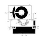
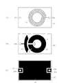
識別タグのリーダライタ用アンテナは、励磁コイル11と、共振回路12、補助電極13とを備えてなる(図1、図2)。ただし、図2(A)〜(C)は、それぞれ励磁コイル11用の基板21、共振回路12、補助電極13用の基板22、グラウンド層14用の基板23の平面図である。 The reader / writer antenna of the identification tag includes an
励磁コイル11は、基板21上において、円形の複数ターンの二次元のスパイラルパターンとして形成されている。励磁コイル11の内側の一端は、開放端となっており、外側の一端は、基板21の一端部のスルーホール21aに引き出されている。なお、基板21の他端部には、スルーホール21aと対になる別のスルーホール21bが形成されている。 The
共振回路12は、基板21と同形同大の基板22上において、円形の1ターンのループパターンとして形成されている。共振回路12は、十分大きな幅wに形成され、両端は、ギャップgを介して対向している。 The
補助電極13は、共振回路12用の基板22上において、共振回路12の外周に近接して、共振回路12と同心の略円弧状のランドパターンとして形成されている。補助電極13、共振回路12の間には、間隔dが形成されており、補助電極13は、スルーホール22aに引き出されている。なお、スルーホール22aは、基板21上のスルーホール21bに対応している。 The
励磁コイル11、共振回路12、補助電極13には、基板21、22と同形同大の基板23に形成するグラウンド層14が付加されている。グラウンド層14は、基板23のほぼ全面を覆う接地パターンとして形成され、基板23の両端部には、スルーホール21a、スルーホール21b、22aにそれぞれ対応する一対のスルーホール23a、23bが形成されている。なお、スルーホール23a、23bには、それぞれランド23cが付設されている。 A
励磁コイル11用の基板21は、たとえばリジッドなセラミックス基板であり、他の基板22、23は、それぞれたとえばフレキシブルなポリイミドフィルム基板である。基板21、22、23は、基板21の両側に基板23、22を配置して一体に積層され、したがって、励磁コイル11と、共振回路12、補助電極13とは、グラウンド層14を付加する一体の多層プリント板となっている。なお、このとき、励磁コイル11、共振回路12は、互いにほぼ同位置に重なるものとする(図3)。また、励磁コイル11の一端を引き出すスルーホール21aは、基板23のスルーホール23aに電気的に接続され、補助電極13を引き出すスルーホール22aは、基板21のスルーホール21bを介してスルーホール23bに電気的に接続される。すなわち、スルーホール23a、23bに付設するランド23c、23cは、それぞれ励磁コイル11用の外部端子T1 、補助電極13用の外部端子T2 として利用することができる。 The
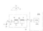
励磁コイル11は、外部端子T1 、結合用のコンデンサCo を介してリーダライタRWの本体部RW1 に接続される(図4)。また、補助電極13には、外部端子T2 を介し、可変コンデンサCv が接続される。なお、図4において、励磁コイル11は、基板21上のストレイ容量Cs が共振用のコンデンサとなっており、本体部RW1 からの搬送周波数の最高値にほぼ共振している。また、共振回路12は、両端のギャップgによって共振用のコンデンサCg が形成されており、相互インダクタンスMを介し、励磁コイル11に電磁結合している。さらに、励磁コイル11、補助電極13の間の間隔dは、両者を容量結合させる結合用のコンデンサCd を形成している。 The
なお、リーダライタRWの本体部RW1 は、リーダライタRWからの情報伝達用の電波を出力する電力増幅部と、識別タグP内のICチップP1 から伝達される情報を読み取る情報入力部との双方を含むものとする。ただし、情報入力部は、リーダライタRWからの電波によってICチップP1 が作動し、リーダライタRWからの電波が負荷変調されることにより、ICチップP1 からの情報を読み取ることができる。なお、ICチップP1 は、共振回路12のほぼ中心線上に位置させて作動させるものとする(図1)。 The main body RW1 of the reader / writer RW includes both a power amplifying unit that outputs radio waves for information transmission from the reader / writer RW and an information input unit that reads information transmitted from the IC chip P1 in the identification tag P. Shall be included. However, the information input unit can read information from the IC chip P1 when the IC chip P1 is operated by the radio wave from the reader / writer RW and the radio wave from the reader / writer RW is load-modulated. It is assumed that the IC chip P1 is operated by being positioned substantially on the center line of the resonance circuit 12 (FIG. 1).
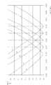
共振回路12の外径3.0mm、内径1.0mm、したがって幅w=1.0mm、ギャップg=0.05mmとし、励磁コイル11を共振回路12の幅w内に重なるサイズの4ターンのスパイラルパターンとして、可変コンデンサCv =0.5〜3pFに変化させるとき、リーダライタRWの本体部RW1 側からみた定在波比SWRの変化データの一例を図5に示す。ただし、図5において、曲線(1)〜(5)は、可変コンデンサCv を最小値から最大値まで変化させた場合を順に示している。すなわち、可変コンデンサCv =0.5〜3pFに対し、アンテナ全体としての共振周波数F=2440〜2460MHz の範囲に滑らかに変化させることができる。なお、このとき、励磁コイル11の共振周波数F1 ≒2470MHz であった。 The
そこで、リーダライタRWは、本体部RW1 からの電波の搬送周波数を変化させるとともに、それに連動させて可変コンデンサCv の容量を変化させることにより、共振回路12の共振周波数Fを搬送周波数に一致させ、共振回路12の放射エレメントとしての性能を最大に維持することが可能である。すなわち、リーダライタRWは、識別タグPを形成する基材の材質により、ICチップP1 上のチップアンテナや、識別タグP内の図示しない共振回路(ブースタアンテナ)の共振周波数が変動しても、識別タグPに対する情報伝達距離を最大に維持することができる。リーダライタRWは、ICチップP1 からのレスポンスが最良となる搬送周波数を見出し、その搬送周波数の電波による情報伝達を自動的に実現することができるからである。 Therefore, the reader / writer RW changes the carrier frequency of the radio wave from the main body RW1 and changes the capacitance of the variable capacitor Cv in conjunction with it to match the resonance frequency F of the
励磁コイル11、共振回路12は、円形に代えて、多角形や楕円形などの他の任意の二次元形状に代えてもよい。また、励磁コイル11、共振回路12のそれぞれの形状、大きさや、両者の相対位置関係は、両者間に所定の電磁結合を実現し得る限り、任意に変更することができる。 The
また、励磁コイル11用の基板21、共振回路12、補助電極13用の基板22、グラウンド層14用の基板23は、その積層順序を違わせることができる(図6(A)、(B))。ただし、図6(A)は、図1の積層順序を示している。また、図4(B)の積層順序であれば、基板21、23のいずれかを両面プリント基板とすることにより、基板22を省略することができ(図6(C)、(D))、図6(A)の積層順序であれば、基板21を省略することができる(図示省略)。なお、図6(A)〜(D)において、グラウンド層14は、励磁コイル11、共振回路12、補助電極13を含む多層プリント板の下面に代えて、上面に配設してもよい。また、グラウンド層14は、これを省略してもよい。 Further, the
なお、励磁コイル11、共振回路12、補助電極13を含む各導体パターンは、印刷、エッチング等の任意のプリント配線板用の手法により形成することができる。 Each conductor pattern including the
P…識別タグ
RW…リーダライタ
g…ギャップ
d…間隔
Cg 、Cd …コンデンサ
Cs …ストレイ容量
Cv …可変コンデンサ
11…励磁コイル
12…共振回路
13…補助電極
14…グラウンド層
特許出願人 株式会社 エフ・イー・シー
代理人 弁理士 松 田 忠 秋
P ... Identification tag RW ... Reader / writer g ... Gap d ... Spacing Cg, Cd ... Capacitor Cs ... Stray capacity Cv ...
Patent applicant F.C. Co., Ltd.
Attorney Tadaaki Matsuda, Attorney
Claims (6)
Translated fromJapanese6. The identification tag reader / writer antenna according to claim 5, wherein a ground layer is added to one side.
Priority Applications (1)
| Application Number | Priority Date | Filing Date | Title |
|---|---|---|---|
| JP2004007967AJP4174801B2 (en) | 2004-01-15 | 2004-01-15 | Identification tag reader / writer antenna |
Applications Claiming Priority (1)
| Application Number | Priority Date | Filing Date | Title |
|---|---|---|---|
| JP2004007967AJP4174801B2 (en) | 2004-01-15 | 2004-01-15 | Identification tag reader / writer antenna |
Publications (2)
| Publication Number | Publication Date |
|---|---|
| JP2005204038Atrue JP2005204038A (en) | 2005-07-28 |
| JP4174801B2 JP4174801B2 (en) | 2008-11-05 |
Family
ID=34821462
Family Applications (1)
| Application Number | Title | Priority Date | Filing Date |
|---|---|---|---|
| JP2004007967AExpired - Fee RelatedJP4174801B2 (en) | 2004-01-15 | 2004-01-15 | Identification tag reader / writer antenna |
Country Status (1)
| Country | Link |
|---|---|
| JP (1) | JP4174801B2 (en) |
Cited By (61)
| Publication number | Priority date | Publication date | Assignee | Title |
|---|---|---|---|---|
| JP2008259269A (en)* | 2007-04-02 | 2008-10-23 | Sony Corp | Controller |
| JP2010051017A (en)* | 2006-01-19 | 2010-03-04 | Murata Mfg Co Ltd | Power supply circuit |
| WO2011118379A1 (en)* | 2010-03-24 | 2011-09-29 | 株式会社村田製作所 | Rfid system |
| WO2012032974A1 (en)* | 2010-09-06 | 2012-03-15 | 株式会社村田製作所 | Rfid module and rfid device |
| US20120306714A1 (en)* | 2010-04-12 | 2012-12-06 | Murata Manufacturing Co., Ltd. | Antenna apparatus and communication terminal |
| US8336786B2 (en) | 2010-03-12 | 2012-12-25 | Murata Manufacturing Co., Ltd. | Wireless communication device and metal article |
| US8406686B2 (en) | 2006-06-08 | 2013-03-26 | Sony Mobile Communications Japan, Inc. | Wireless communication terminal apparatus and method of controlling same |
| US8413907B2 (en) | 2007-07-17 | 2013-04-09 | Murata Manufacturing Co., Ltd. | Wireless IC device and electronic apparatus |
| US8424762B2 (en) | 2007-04-14 | 2013-04-23 | Murata Manufacturing Co., Ltd. | Wireless IC device and component for wireless IC device |
| US8424769B2 (en) | 2010-07-08 | 2013-04-23 | Murata Manufacturing Co., Ltd. | Antenna and RFID device |
| US20130113662A1 (en)* | 2009-04-21 | 2013-05-09 | Murata Manufacturing Co., Ltd. | Antenna device and method of setting resonant frequency of antenna device |
| US8544759B2 (en) | 2009-01-09 | 2013-10-01 | Murata Manufacturing., Ltd. | Wireless IC device, wireless IC module and method of manufacturing wireless IC module |
| US8552870B2 (en) | 2007-07-09 | 2013-10-08 | Murata Manufacturing Co., Ltd. | Wireless IC device |
| US8590797B2 (en) | 2008-05-21 | 2013-11-26 | Murata Manufacturing Co., Ltd. | Wireless IC device |
| US8602310B2 (en) | 2010-03-03 | 2013-12-10 | Murata Manufacturing Co., Ltd. | Radio communication device and radio communication terminal |
| US8613395B2 (en) | 2011-02-28 | 2013-12-24 | Murata Manufacturing Co., Ltd. | Wireless communication device |
| US8676117B2 (en) | 2006-01-19 | 2014-03-18 | Murata Manufacturing Co., Ltd. | Wireless IC device and component for wireless IC device |
| US8690070B2 (en) | 2009-04-14 | 2014-04-08 | Murata Manufacturing Co., Ltd. | Wireless IC device component and wireless IC device |
| US8704716B2 (en) | 2009-11-20 | 2014-04-22 | Murata Manufacturing Co., Ltd. | Antenna device and mobile communication terminal |
| US8720789B2 (en) | 2012-01-30 | 2014-05-13 | Murata Manufacturing Co., Ltd. | Wireless IC device |
| US8740093B2 (en) | 2011-04-13 | 2014-06-03 | Murata Manufacturing Co., Ltd. | Radio IC device and radio communication terminal |
| US8770489B2 (en) | 2011-07-15 | 2014-07-08 | Murata Manufacturing Co., Ltd. | Radio communication device |
| US8797225B2 (en) | 2011-03-08 | 2014-08-05 | Murata Manufacturing Co., Ltd. | Antenna device and communication terminal apparatus |
| US8797148B2 (en) | 2008-03-03 | 2014-08-05 | Murata Manufacturing Co., Ltd. | Radio frequency IC device and radio communication system |
| US8814056B2 (en) | 2011-07-19 | 2014-08-26 | Murata Manufacturing Co., Ltd. | Antenna device, RFID tag, and communication terminal apparatus |
| US8853549B2 (en) | 2009-09-30 | 2014-10-07 | Murata Manufacturing Co., Ltd. | Circuit substrate and method of manufacturing same |
| US8870077B2 (en) | 2008-08-19 | 2014-10-28 | Murata Manufacturing Co., Ltd. | Wireless IC device and method for manufacturing same |
| US8878739B2 (en) | 2011-07-14 | 2014-11-04 | Murata Manufacturing Co., Ltd. | Wireless communication device |
| US8905296B2 (en) | 2011-12-01 | 2014-12-09 | Murata Manufacturing Co., Ltd. | Wireless integrated circuit device and method of manufacturing the same |
| US8917211B2 (en) | 2008-11-17 | 2014-12-23 | Murata Manufacturing Co., Ltd. | Antenna and wireless IC device |
| US8937576B2 (en) | 2011-04-05 | 2015-01-20 | Murata Manufacturing Co., Ltd. | Wireless communication device |
| US8944335B2 (en) | 2010-09-30 | 2015-02-03 | Murata Manufacturing Co., Ltd. | Wireless IC device |
| US8981906B2 (en) | 2010-08-10 | 2015-03-17 | Murata Manufacturing Co., Ltd. | Printed wiring board and wireless communication system |
| US8991713B2 (en) | 2011-01-14 | 2015-03-31 | Murata Manufacturing Co., Ltd. | RFID chip package and RFID tag |
| US9024837B2 (en) | 2010-03-31 | 2015-05-05 | Murata Manufacturing Co., Ltd. | Antenna and wireless communication device |
| US9024725B2 (en) | 2009-11-04 | 2015-05-05 | Murata Manufacturing Co., Ltd. | Communication terminal and information processing system |
| US9104950B2 (en) | 2009-01-30 | 2015-08-11 | Murata Manufacturing Co., Ltd. | Antenna and wireless IC device |
| US9117157B2 (en) | 2009-10-02 | 2015-08-25 | Murata Manufacturing Co., Ltd. | Wireless IC device and electromagnetic coupling module |
| JP2015181241A (en)* | 2010-02-26 | 2015-10-15 | デカ・プロダクツ・リミテッド・パートナーシップ | Rfid system with eddy current trap |
| US9165239B2 (en) | 2006-04-26 | 2015-10-20 | Murata Manufacturing Co., Ltd. | Electromagnetic-coupling-module-attached article |
| US9166291B2 (en) | 2010-10-12 | 2015-10-20 | Murata Manufacturing Co., Ltd. | Antenna device and communication terminal apparatus |
| JP2015222866A (en)* | 2014-05-22 | 2015-12-10 | パナソニックIpマネジメント株式会社 | Signal coupler |
| JP2015222867A (en)* | 2014-05-22 | 2015-12-10 | パナソニックIpマネジメント株式会社 | Signal combiner |
| US9236651B2 (en) | 2010-10-21 | 2016-01-12 | Murata Manufacturing Co., Ltd. | Communication terminal device |
| US9281873B2 (en) | 2008-05-26 | 2016-03-08 | Murata Manufacturing Co., Ltd. | Wireless IC device system and method of determining authenticity of wireless IC device |
| US9378452B2 (en) | 2011-05-16 | 2016-06-28 | Murata Manufacturing Co., Ltd. | Radio IC device |
| US9543642B2 (en) | 2011-09-09 | 2017-01-10 | Murata Manufacturing Co., Ltd. | Antenna device and wireless device |
| US9558384B2 (en) | 2010-07-28 | 2017-01-31 | Murata Manufacturing Co., Ltd. | Antenna apparatus and communication terminal instrument |
| US9692128B2 (en) | 2012-02-24 | 2017-06-27 | Murata Manufacturing Co., Ltd. | Antenna device and wireless communication device |
| US9761923B2 (en) | 2011-01-05 | 2017-09-12 | Murata Manufacturing Co., Ltd. | Wireless communication device |
| US9830552B2 (en) | 2007-07-18 | 2017-11-28 | Murata Manufacturing Co., Ltd. | Radio IC device |
| US10013650B2 (en) | 2010-03-03 | 2018-07-03 | Murata Manufacturing Co., Ltd. | Wireless communication module and wireless communication device |
| US10235544B2 (en) | 2012-04-13 | 2019-03-19 | Murata Manufacturing Co., Ltd. | Inspection method and inspection device for RFID tag |
| US10518518B2 (en) | 2013-01-18 | 2019-12-31 | Féinics Amatech Teoranta | Smart cards with metal layer(s) and methods of manufacture |
| US10552722B2 (en) | 2014-08-10 | 2020-02-04 | Féinics Amatech Teoranta | Smartcard with coupling frame antenna |
| US10599972B2 (en) | 2013-01-18 | 2020-03-24 | Féinics Amatech Teoranta | Smartcard constructions and methods |
| US10733494B2 (en) | 2014-08-10 | 2020-08-04 | Féinics Amatech Teoranta | Contactless metal card constructions |
| US10824931B2 (en) | 2012-08-30 | 2020-11-03 | Féinics Amatech Teoranta | Contactless smartcards with multiple coupling frames |
| US11354558B2 (en) | 2013-01-18 | 2022-06-07 | Amatech Group Limited | Contactless smartcards with coupling frames |
| US11354560B2 (en) | 2013-01-18 | 2022-06-07 | Amatech Group Limited | Smartcards with multiple coupling frames |
| US11551051B2 (en) | 2013-01-18 | 2023-01-10 | Amatech Group Limiied | Coupling frames for smartcards with various module opening shapes |
- 2004
- 2004-01-15JPJP2004007967Apatent/JP4174801B2/ennot_activeExpired - Fee Related
Cited By (84)
| Publication number | Priority date | Publication date | Assignee | Title |
|---|---|---|---|---|
| JP2010051017A (en)* | 2006-01-19 | 2010-03-04 | Murata Mfg Co Ltd | Power supply circuit |
| US8676117B2 (en) | 2006-01-19 | 2014-03-18 | Murata Manufacturing Co., Ltd. | Wireless IC device and component for wireless IC device |
| US8725071B2 (en) | 2006-01-19 | 2014-05-13 | Murata Manufacturing Co., Ltd. | Wireless IC device and component for wireless IC device |
| US9165239B2 (en) | 2006-04-26 | 2015-10-20 | Murata Manufacturing Co., Ltd. | Electromagnetic-coupling-module-attached article |
| US8406686B2 (en) | 2006-06-08 | 2013-03-26 | Sony Mobile Communications Japan, Inc. | Wireless communication terminal apparatus and method of controlling same |
| JP2008259269A (en)* | 2007-04-02 | 2008-10-23 | Sony Corp | Controller |
| US8424762B2 (en) | 2007-04-14 | 2013-04-23 | Murata Manufacturing Co., Ltd. | Wireless IC device and component for wireless IC device |
| US8662403B2 (en) | 2007-07-04 | 2014-03-04 | Murata Manufacturing Co., Ltd. | Wireless IC device and component for wireless IC device |
| US8552870B2 (en) | 2007-07-09 | 2013-10-08 | Murata Manufacturing Co., Ltd. | Wireless IC device |
| US8413907B2 (en) | 2007-07-17 | 2013-04-09 | Murata Manufacturing Co., Ltd. | Wireless IC device and electronic apparatus |
| US9830552B2 (en) | 2007-07-18 | 2017-11-28 | Murata Manufacturing Co., Ltd. | Radio IC device |
| US8797148B2 (en) | 2008-03-03 | 2014-08-05 | Murata Manufacturing Co., Ltd. | Radio frequency IC device and radio communication system |
| US9022295B2 (en) | 2008-05-21 | 2015-05-05 | Murata Manufacturing Co., Ltd. | Wireless IC device |
| US8973841B2 (en) | 2008-05-21 | 2015-03-10 | Murata Manufacturing Co., Ltd. | Wireless IC device |
| US8590797B2 (en) | 2008-05-21 | 2013-11-26 | Murata Manufacturing Co., Ltd. | Wireless IC device |
| US9281873B2 (en) | 2008-05-26 | 2016-03-08 | Murata Manufacturing Co., Ltd. | Wireless IC device system and method of determining authenticity of wireless IC device |
| US8870077B2 (en) | 2008-08-19 | 2014-10-28 | Murata Manufacturing Co., Ltd. | Wireless IC device and method for manufacturing same |
| US8917211B2 (en) | 2008-11-17 | 2014-12-23 | Murata Manufacturing Co., Ltd. | Antenna and wireless IC device |
| US8544759B2 (en) | 2009-01-09 | 2013-10-01 | Murata Manufacturing., Ltd. | Wireless IC device, wireless IC module and method of manufacturing wireless IC module |
| US9104950B2 (en) | 2009-01-30 | 2015-08-11 | Murata Manufacturing Co., Ltd. | Antenna and wireless IC device |
| US8690070B2 (en) | 2009-04-14 | 2014-04-08 | Murata Manufacturing Co., Ltd. | Wireless IC device component and wireless IC device |
| US8876010B2 (en) | 2009-04-14 | 2014-11-04 | Murata Manufacturing Co., Ltd | Wireless IC device component and wireless IC device |
| US8976075B2 (en) | 2009-04-21 | 2015-03-10 | Murata Manufacturing Co., Ltd. | Antenna device and method of setting resonant frequency of antenna device |
| US9203157B2 (en)* | 2009-04-21 | 2015-12-01 | Murata Manufacturing Co., Ltd. | Antenna device and method of setting resonant frequency of antenna device |
| JP5360202B2 (en)* | 2009-04-21 | 2013-12-04 | 株式会社村田製作所 | Antenna device |
| US20130300622A1 (en)* | 2009-04-21 | 2013-11-14 | Murata Manufacturing Co., Ltd. | Antenna device and method of setting resonant frequency of antenna device |
| US9564678B2 (en)* | 2009-04-21 | 2017-02-07 | Murata Manufacturing Co., Ltd. | Antenna device and method of setting resonant frequency of antenna device |
| US20130234905A1 (en)* | 2009-04-21 | 2013-09-12 | Murata Manufacturing Co., Ltd. | Antenna device and method of setting resonant frequency of antenna device |
| US20130113662A1 (en)* | 2009-04-21 | 2013-05-09 | Murata Manufacturing Co., Ltd. | Antenna device and method of setting resonant frequency of antenna device |
| US9000619B2 (en) | 2009-04-21 | 2015-04-07 | Murata Manufacturing Co., Ltd. | Antenna apparatus |
| US8853549B2 (en) | 2009-09-30 | 2014-10-07 | Murata Manufacturing Co., Ltd. | Circuit substrate and method of manufacturing same |
| US9117157B2 (en) | 2009-10-02 | 2015-08-25 | Murata Manufacturing Co., Ltd. | Wireless IC device and electromagnetic coupling module |
| US9024725B2 (en) | 2009-11-04 | 2015-05-05 | Murata Manufacturing Co., Ltd. | Communication terminal and information processing system |
| US8704716B2 (en) | 2009-11-20 | 2014-04-22 | Murata Manufacturing Co., Ltd. | Antenna device and mobile communication terminal |
| JP2015181241A (en)* | 2010-02-26 | 2015-10-15 | デカ・プロダクツ・リミテッド・パートナーシップ | Rfid system with eddy current trap |
| US10013650B2 (en) | 2010-03-03 | 2018-07-03 | Murata Manufacturing Co., Ltd. | Wireless communication module and wireless communication device |
| US8602310B2 (en) | 2010-03-03 | 2013-12-10 | Murata Manufacturing Co., Ltd. | Radio communication device and radio communication terminal |
| US8336786B2 (en) | 2010-03-12 | 2012-12-25 | Murata Manufacturing Co., Ltd. | Wireless communication device and metal article |
| US8528829B2 (en) | 2010-03-12 | 2013-09-10 | Murata Manufacturing Co., Ltd. | Wireless communication device and metal article |
| GB2491447B (en)* | 2010-03-24 | 2014-10-22 | Murata Manufacturing Co | RFID system |
| WO2011118379A1 (en)* | 2010-03-24 | 2011-09-29 | 株式会社村田製作所 | Rfid system |
| JP5370581B2 (en)* | 2010-03-24 | 2013-12-18 | 株式会社村田製作所 | RFID system |
| GB2491447A (en)* | 2010-03-24 | 2012-12-05 | Murata Manufacturing Co | RFID system |
| US9727765B2 (en) | 2010-03-24 | 2017-08-08 | Murata Manufacturing Co., Ltd. | RFID system including a reader/writer and RFID tag |
| US9024837B2 (en) | 2010-03-31 | 2015-05-05 | Murata Manufacturing Co., Ltd. | Antenna and wireless communication device |
| US9595749B2 (en)* | 2010-04-12 | 2017-03-14 | Murata Manufacturing Co., Ltd. | Antenna apparatus and communication terminal |
| US20120306714A1 (en)* | 2010-04-12 | 2012-12-06 | Murata Manufacturing Co., Ltd. | Antenna apparatus and communication terminal |
| US8424769B2 (en) | 2010-07-08 | 2013-04-23 | Murata Manufacturing Co., Ltd. | Antenna and RFID device |
| US9558384B2 (en) | 2010-07-28 | 2017-01-31 | Murata Manufacturing Co., Ltd. | Antenna apparatus and communication terminal instrument |
| US8981906B2 (en) | 2010-08-10 | 2015-03-17 | Murata Manufacturing Co., Ltd. | Printed wiring board and wireless communication system |
| JP5062372B2 (en)* | 2010-09-06 | 2012-10-31 | 株式会社村田製作所 | RFID module and RFID device |
| WO2012032974A1 (en)* | 2010-09-06 | 2012-03-15 | 株式会社村田製作所 | Rfid module and rfid device |
| GB2496713A (en)* | 2010-09-06 | 2013-05-22 | Murata Manufacturing Co | RFID module and RFID device |
| US8944335B2 (en) | 2010-09-30 | 2015-02-03 | Murata Manufacturing Co., Ltd. | Wireless IC device |
| US9166291B2 (en) | 2010-10-12 | 2015-10-20 | Murata Manufacturing Co., Ltd. | Antenna device and communication terminal apparatus |
| US9236651B2 (en) | 2010-10-21 | 2016-01-12 | Murata Manufacturing Co., Ltd. | Communication terminal device |
| US9761923B2 (en) | 2011-01-05 | 2017-09-12 | Murata Manufacturing Co., Ltd. | Wireless communication device |
| US8991713B2 (en) | 2011-01-14 | 2015-03-31 | Murata Manufacturing Co., Ltd. | RFID chip package and RFID tag |
| US8960561B2 (en) | 2011-02-28 | 2015-02-24 | Murata Manufacturing Co., Ltd. | Wireless communication device |
| US8613395B2 (en) | 2011-02-28 | 2013-12-24 | Murata Manufacturing Co., Ltd. | Wireless communication device |
| US8757502B2 (en) | 2011-02-28 | 2014-06-24 | Murata Manufacturing Co., Ltd. | Wireless communication device |
| US8797225B2 (en) | 2011-03-08 | 2014-08-05 | Murata Manufacturing Co., Ltd. | Antenna device and communication terminal apparatus |
| US8937576B2 (en) | 2011-04-05 | 2015-01-20 | Murata Manufacturing Co., Ltd. | Wireless communication device |
| US8740093B2 (en) | 2011-04-13 | 2014-06-03 | Murata Manufacturing Co., Ltd. | Radio IC device and radio communication terminal |
| US9378452B2 (en) | 2011-05-16 | 2016-06-28 | Murata Manufacturing Co., Ltd. | Radio IC device |
| US8878739B2 (en) | 2011-07-14 | 2014-11-04 | Murata Manufacturing Co., Ltd. | Wireless communication device |
| US8770489B2 (en) | 2011-07-15 | 2014-07-08 | Murata Manufacturing Co., Ltd. | Radio communication device |
| US8814056B2 (en) | 2011-07-19 | 2014-08-26 | Murata Manufacturing Co., Ltd. | Antenna device, RFID tag, and communication terminal apparatus |
| US9543642B2 (en) | 2011-09-09 | 2017-01-10 | Murata Manufacturing Co., Ltd. | Antenna device and wireless device |
| US8905296B2 (en) | 2011-12-01 | 2014-12-09 | Murata Manufacturing Co., Ltd. | Wireless integrated circuit device and method of manufacturing the same |
| US8720789B2 (en) | 2012-01-30 | 2014-05-13 | Murata Manufacturing Co., Ltd. | Wireless IC device |
| US9692128B2 (en) | 2012-02-24 | 2017-06-27 | Murata Manufacturing Co., Ltd. | Antenna device and wireless communication device |
| US10235544B2 (en) | 2012-04-13 | 2019-03-19 | Murata Manufacturing Co., Ltd. | Inspection method and inspection device for RFID tag |
| US10824931B2 (en) | 2012-08-30 | 2020-11-03 | Féinics Amatech Teoranta | Contactless smartcards with multiple coupling frames |
| US11354558B2 (en) | 2013-01-18 | 2022-06-07 | Amatech Group Limited | Contactless smartcards with coupling frames |
| US10518518B2 (en) | 2013-01-18 | 2019-12-31 | Féinics Amatech Teoranta | Smart cards with metal layer(s) and methods of manufacture |
| US10599972B2 (en) | 2013-01-18 | 2020-03-24 | Féinics Amatech Teoranta | Smartcard constructions and methods |
| US11354560B2 (en) | 2013-01-18 | 2022-06-07 | Amatech Group Limited | Smartcards with multiple coupling frames |
| US11551051B2 (en) | 2013-01-18 | 2023-01-10 | Amatech Group Limiied | Coupling frames for smartcards with various module opening shapes |
| US11836565B2 (en) | 2013-01-18 | 2023-12-05 | Amatech Group Limited | Smartcards with multiple coupling frames |
| JP2015222866A (en)* | 2014-05-22 | 2015-12-10 | パナソニックIpマネジメント株式会社 | Signal coupler |
| JP2015222867A (en)* | 2014-05-22 | 2015-12-10 | パナソニックIpマネジメント株式会社 | Signal combiner |
| US10552722B2 (en) | 2014-08-10 | 2020-02-04 | Féinics Amatech Teoranta | Smartcard with coupling frame antenna |
| US10733494B2 (en) | 2014-08-10 | 2020-08-04 | Féinics Amatech Teoranta | Contactless metal card constructions |
Also Published As
| Publication number | Publication date |
|---|---|
| JP4174801B2 (en) | 2008-11-05 |
Similar Documents
| Publication | Publication Date | Title |
|---|---|---|
| JP4174801B2 (en) | Identification tag reader / writer antenna | |
| US9016592B2 (en) | Antenna device and communication terminal apparatus | |
| JP4404166B2 (en) | Wireless IC device | |
| US7954722B2 (en) | IC tag and inlet for IC tag | |
| US7830311B2 (en) | Wireless IC device and electronic device | |
| JP5131413B2 (en) | Antenna device and communication terminal device | |
| JP5370616B2 (en) | Wireless communication device | |
| US10396429B2 (en) | Wireless communication device | |
| US9104950B2 (en) | Antenna and wireless IC device | |
| JP6590122B1 (en) | RFID tag and article to which RFID tag is attached | |
| JP5434920B2 (en) | Wireless IC device and manufacturing method thereof | |
| CN103370886B (en) | Wireless communication device | |
| JP2008072243A (en) | Wireless ic device | |
| EP1862951A1 (en) | IC tag and inlet for IC tag | |
| CN103370834A (en) | Wireless communication device | |
| JP2011193245A (en) | Antenna device, radio communication device and radio communication terminal | |
| US8720789B2 (en) | Wireless IC device | |
| US8941552B2 (en) | Composite printed wiring board and wireless communication system | |
| JP5034736B2 (en) | Wireless IC device | |
| JP5162988B2 (en) | Wireless IC device and manufacturing method thereof |
Legal Events
| Date | Code | Title | Description |
|---|---|---|---|
| A621 | Written request for application examination | Free format text:JAPANESE INTERMEDIATE CODE: A621 Effective date:20061117 | |
| A131 | Notification of reasons for refusal | Free format text:JAPANESE INTERMEDIATE CODE: A131 Effective date:20080617 | |
| A521 | Request for written amendment filed | Free format text:JAPANESE INTERMEDIATE CODE: A523 Effective date:20080709 | |
| TRDD | Decision of grant or rejection written | ||
| A01 | Written decision to grant a patent or to grant a registration (utility model) | Free format text:JAPANESE INTERMEDIATE CODE: A01 Effective date:20080805 | |
| A01 | Written decision to grant a patent or to grant a registration (utility model) | Free format text:JAPANESE INTERMEDIATE CODE: A01 | |
| A61 | First payment of annual fees (during grant procedure) | Free format text:JAPANESE INTERMEDIATE CODE: A61 Effective date:20080808 | |
| FPAY | Renewal fee payment (event date is renewal date of database) | Free format text:PAYMENT UNTIL: 20110829 Year of fee payment:3 | |
| R150 | Certificate of patent or registration of utility model | Free format text:JAPANESE INTERMEDIATE CODE: R150 | |
| LAPS | Cancellation because of no payment of annual fees |