JP2005202280A - Reflector and liquid crystal display device - Google Patents
Reflector and liquid crystal display deviceDownload PDFInfo
- Publication number
- JP2005202280A JP2005202280AJP2004010428AJP2004010428AJP2005202280AJP 2005202280 AJP2005202280 AJP 2005202280AJP 2004010428 AJP2004010428 AJP 2004010428AJP 2004010428 AJP2004010428 AJP 2004010428AJP 2005202280 AJP2005202280 AJP 2005202280A
- Authority
- JP
- Japan
- Prior art keywords
- reflector
- liquid crystal
- crystal display
- display device
- substrate
- Prior art date
- Legal status (The legal status is an assumption and is not a legal conclusion. Google has not performed a legal analysis and makes no representation as to the accuracy of the status listed.)
- Withdrawn
Links
- 239000004973liquid crystal related substanceSubstances0.000titleclaimsabstractdescription34
- 239000000758substrateSubstances0.000claimsdescription26
- 238000004519manufacturing processMethods0.000abstractdescription9
- 239000012634fragmentSubstances0.000abstract2
- 239000011347resinSubstances0.000description6
- 229920005989resinPolymers0.000description6
- 238000010586diagramMethods0.000description3
- 238000000034methodMethods0.000description2
- 238000002310reflectometryMethods0.000description2
- 229910052709silverInorganic materials0.000description2
- 229910004298SiO 2Inorganic materials0.000description1
- 230000015572biosynthetic processEffects0.000description1
- 239000011248coating agentSubstances0.000description1
- 238000000576coating methodMethods0.000description1
- 238000000151depositionMethods0.000description1
- 238000004049embossingMethods0.000description1
- 239000011521glassSubstances0.000description1
- 239000000463materialSubstances0.000description1
- 239000002184metalSubstances0.000description1
- 229910052751metalInorganic materials0.000description1
- 125000006850spacer groupChemical group0.000description1
Images


Classifications
- G—PHYSICS
- G02—OPTICS
- G02F—OPTICAL DEVICES OR ARRANGEMENTS FOR THE CONTROL OF LIGHT BY MODIFICATION OF THE OPTICAL PROPERTIES OF THE MEDIA OF THE ELEMENTS INVOLVED THEREIN; NON-LINEAR OPTICS; FREQUENCY-CHANGING OF LIGHT; OPTICAL LOGIC ELEMENTS; OPTICAL ANALOGUE/DIGITAL CONVERTERS
- G02F1/00—Devices or arrangements for the control of the intensity, colour, phase, polarisation or direction of light arriving from an independent light source, e.g. switching, gating or modulating; Non-linear optics
- G02F1/01—Devices or arrangements for the control of the intensity, colour, phase, polarisation or direction of light arriving from an independent light source, e.g. switching, gating or modulating; Non-linear optics for the control of the intensity, phase, polarisation or colour
- G02F1/13—Devices or arrangements for the control of the intensity, colour, phase, polarisation or direction of light arriving from an independent light source, e.g. switching, gating or modulating; Non-linear optics for the control of the intensity, phase, polarisation or colour based on liquid crystals, e.g. single liquid crystal display cells
- G02F1/133—Constructional arrangements; Operation of liquid crystal cells; Circuit arrangements
- G02F1/1333—Constructional arrangements; Manufacturing methods
- G02F1/1335—Structural association of cells with optical devices, e.g. polarisers or reflectors
- G02F1/133553—Reflecting elements
- A—HUMAN NECESSITIES
- A47—FURNITURE; DOMESTIC ARTICLES OR APPLIANCES; COFFEE MILLS; SPICE MILLS; SUCTION CLEANERS IN GENERAL
- A47G—HOUSEHOLD OR TABLE EQUIPMENT
- A47G23/00—Other table equipment
- A47G23/06—Serving trays
- G—PHYSICS
- G02—OPTICS
- G02B—OPTICAL ELEMENTS, SYSTEMS OR APPARATUS
- G02B5/00—Optical elements other than lenses
- G02B5/12—Reflex reflectors
- G02B5/136—Reflex reflectors plural reflecting elements forming part of a unitary body
Landscapes
- Physics & Mathematics (AREA)
- Nonlinear Science (AREA)
- General Physics & Mathematics (AREA)
- Optics & Photonics (AREA)
- Mathematical Physics (AREA)
- Chemical & Material Sciences (AREA)
- Crystallography & Structural Chemistry (AREA)
- Optical Elements Other Than Lenses (AREA)
- Liquid Crystal (AREA)
- Devices For Indicating Variable Information By Combining Individual Elements (AREA)
Abstract
Description
Translated fromJapanese本発明は、表面に多数の凹部を形成した基板の表面に反射膜を成膜した反射体、およびこれを用いた液晶表示装置に関する。 The present invention relates to a reflector having a reflective film formed on the surface of a substrate having a large number of recesses on the surface, and a liquid crystal display device using the same.
例えば、携帯電話や携帯用ゲーム機などの携帯電子機器では、そのバッテリ駆動時間が使い勝手に大きく影響するために、消費電力を抑えることができる反射型液晶表示装置を表示部として備えている。反射型液晶表示装置は、その前面から入射する外光を反射するための反射膜を備えており、その形態としては液晶パネルを構成する2枚の基板の間に反射膜を内蔵したものや、透過型の液晶パネルの背面側に半透過膜を備えた反射体を配設したものが知られている。 For example, portable electronic devices such as a mobile phone and a portable game machine have a reflective liquid crystal display device that can suppress power consumption as a display unit because the battery driving time greatly affects usability. The reflection-type liquid crystal display device includes a reflection film for reflecting external light incident from the front surface, and includes a reflection film built-in between two substrates constituting a liquid crystal panel, 2. Description of the Related Art A transmissive liquid crystal panel having a reflector provided with a semi-transmissive film on the back side is known.
光を反射させるための反射体としては、表面に多数の凹部を形成した基板の表面に反射膜を成膜した反射体が知られている。こうした反射体は、多数の凹部の作用によって反射面内でムラなく均一な反射光を得ることができる。 As a reflector for reflecting light, a reflector in which a reflective film is formed on the surface of a substrate on which a large number of concave portions are formed is known. Such a reflector can obtain uniform reflected light evenly within the reflecting surface by the action of a large number of recesses.
このような反射体を製造するには、例えば、下記特許文献1に記載されている方法が挙げられる。即ち、圧子によって凹凸面を備えた母型を製造し、この母型を用いて多数の凹部を備えた基板を転写形成し、その後、反射膜を成膜する方法である。これによって、反射体を効率的に製造することができる。
上述したような、表面に多数の凹部を形成した基板の表面に反射膜を成膜した反射体は、ランダムなサイズの凹部をランダムな配置で形成するのが好ましい。即ち、凹部の配置に規則性ができると、反射体として使用した際にモアレ発生の原因となるからである。従って、モアレ発生を防止するには、必要なサイズの反射面全体に渡ってランダムな大きさの凹部をランダムに配置するのが良い。 As described above, it is preferable that the reflector having the reflective film formed on the surface of the substrate on which a large number of concave portions are formed has the concave portions having a random size formed in a random arrangement. That is, if the arrangement of the recesses is regular, moire occurs when used as a reflector. Therefore, in order to prevent the occurrence of moire, it is preferable to randomly arrange concave portions having a random size over the entire reflective surface having a required size.
しかし一方で、上述したように圧子によって凹凸面を備えた母型を製造し、この母型を用いて多数の凹部を備えた基板を転写形成する場合、必要なサイズの反射面に相当する領域全体にランダムに配置された凹部を備えた母型を製造することは、例えば数ヶ月という日数が掛かってしまい現実的ではない。 However, on the other hand, when a mother die having an uneven surface is manufactured by an indenter as described above, and a substrate having a large number of recesses is transferred using this mother die, an area corresponding to a reflective surface of a necessary size. It is not practical to manufacture a mother die having concave portions randomly arranged on the whole because, for example, it takes several days.
本発明は、上記事情に鑑みてなされたものであって、モアレの発生を防止でき、かつ製造が容易な反射体、ならびにこれを用いた液晶表示を提供することを目的とする。 The present invention has been made in view of the above circumstances, and an object of the present invention is to provide a reflector that can prevent the occurrence of moire and can be easily manufactured, and a liquid crystal display using the reflector.
上記の目的を達成するために、本発明によれば、微細な多数の凹部が規定単位毎にランダムな大きさで形成された基板と、前記基板の一面上に成膜された反射膜とを有する反射体であって、前記規定単位を30〜3000μmに設定し、この規定単位を1ピッチとして繰り返し多数の凹部を形成して、一辺が前記規定単位よりも大きな面に多数の凹部を形成したことを特徴とする反射体が提供される。 In order to achieve the above object, according to the present invention, a substrate in which a large number of minute recesses are formed in random sizes for each specified unit, and a reflective film formed on one surface of the substrate are provided. The prescribed unit is set to 30 to 3000 μm, the prescribed unit is set as one pitch, a large number of concave portions are formed, and a large number of concave portions are formed on a surface having one side larger than the prescribed unit. A reflector is provided.
また、上述した反射体と液晶表示パネルとを備えたことを特徴とする液晶表示装置が提供される。 Also provided is a liquid crystal display device comprising the reflector described above and a liquid crystal display panel.
本発明の反射体によれば、微細な多数の凹部が規定単位毎にランダムな大きさで形成された基板と、この基板の一面上に成膜された反射膜とを有し、反射体小片の一辺の長さである規定単位を30〜3000μmに設定される。そして、液晶表示装置の反射体として用いたときに、モアレ(干渉縞)の発生を効果的に防止することができるとともに、反射体の凹部を転写形成するための母型の製造に要する時間を実用的な範囲に留めることができる。よって、モアレの生じない反射体を短期間にローコストで製造することが可能になる。 According to the reflector of the present invention, the reflector has a substrate on which a large number of minute recesses are formed in random sizes for each specified unit, and a reflector film formed on one surface of the substrate. The prescribed unit which is the length of one side is set to 30 to 3000 μm. And when it is used as a reflector of a liquid crystal display device, the generation of moire (interference fringes) can be effectively prevented, and the time required for manufacturing the mother die for transferring and forming the concave portions of the reflector can be reduced. It can be kept within the practical range. Therefore, it is possible to manufacture a reflector that does not cause moiré at a low cost in a short time.
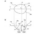
以下、本発明の実施の形態について、図面を交えて説明する。図1は、本発明の反射体の構成を示す部分斜視図であり、図2は、図1に示す反射体の断面模式図であり、図3のAは、図1に示す反射体に形成された凹部の平面構成図であり、図3のBは、図3のAに示すG−G線に沿う断面構成図である。 Hereinafter, embodiments of the present invention will be described with reference to the drawings. FIG. 1 is a partial perspective view showing the configuration of the reflector of the present invention, FIG. 2 is a schematic sectional view of the reflector shown in FIG. 1, and A in FIG. 3 is formed on the reflector shown in FIG. FIG. 3B is a cross-sectional configuration diagram taken along line GG shown in FIG. 3A.
図1のBに示すように、反射体10は基板11と、この基板11の一面11a上に積層されたAlやAg等の高反射率の反射膜12とから概略構成されている。この基板11は、図1のAに示すように、支持層15と、この支持層15上に形成された樹脂層16とから構成されている。樹脂層16は、反射膜12に所定の表面形状、すなわち樹脂層16の凹部13に倣った凹部12aを与えるもので、一面11aに複数の凹部13が設けられている。 As shown in FIG. 1B, the
こうした凹部13によって、図1のBに示すように、反射膜12に凹部12aが形成され、反射膜12にムラの無い均一な反射性を与える。こうした基板11を構成する支持層15は、例えばSiO2コーティング付きのガラス板から構成されれば良く、また、樹脂層16は紫外線硬化性樹脂から構成されていればよい。こうした基板11の厚さは、例えば50μm〜1mmの範囲であれば好ましく、特に100〜700μmの範囲がよい。As shown in FIG. 1B, the
反射膜12は、基板の一面11a上に、例えば、AlやAg等の高反射特性の金属を蒸着して形成すればよく、膜厚は0.05〜0.2μmの範囲が良く、0.08〜0.15μmの範囲が特に好ましい。反射膜12の膜厚が0.05μm未満だと反射率が低下してしまうので好ましくなく、0.2μmを超えると必要以上に成膜コストがかかることや、凹部13によって与えられる凹部12aが小さくなってしまうので好ましくない。 The
凹部13は、基板11の樹脂層16に対して、後ほど詳述する反転金型を用いて型押し加工によって形成されたものであり、図1のB及び図2に示すように、反射膜12上において、各凹部12aの輪郭12c同士が相互に接している。この輪郭12c同士が接する部分は先の尖ったピーク形状に形成され、凹部12a同士の間にある平坦部分12dの領域が少ないのが反射特性上好ましい。 The
また図3に示すように、凹部13の内面は、各々半径が異なる2つの球面の一部である第1曲面13aと、第2曲面13bとを含んでおり、これらの曲面13a,13bを与える球の中心O1,O2は凹部13の最深点Oの法線上に配置されている。第1曲面13aはO1を中心とする半径R1の球面の一部とされ、第2曲面13bはO2を中心とする半径R2の球面の一部とされている。そして、図3のAに示す平面図において、凹部13の最深点Oを通過し、G−G線に直交する直線Hの近傍において第1曲面13aと第2曲面13bとが概ね区画されている。凹部13の深さは例えば0.3〜2.0μm程度に形成されればよい。 As shown in FIG. 3, the inner surface of the
図4は、上述したような構成の反射体10に、図3における図示右側から入射角30°で光を照射し、受光角を反射面に対する正反射の方向である30°を中心として±30°の範囲(0°〜60°;0°が反射体一面の法線方向に相当)で振って反射体10の反射率(%)を測定した結果を示すグラフである。 4 irradiates the
図4に示すグラフから明らかなように、上記構成を備えた反射体10によれば、半径の比較的小さい球面からなる第2曲面13bの傾斜角の絶対値が比較的大きいことから、反射光が広角に散乱されて約15°〜50°の広い受光角範囲で高い反射率を得ることができる。また、半径が比較的大きい球面からなる第1曲面13aにおける反射により、前記第2曲面13bよりも特定方向の狭い範囲に散乱される反射が生じるため、全体として反射率が正反射方向である30°よりも小さい角度で最大となり、そのピークの近傍における反射率も高くなる。 As is apparent from the graph shown in FIG. 4, according to the
その結果、反射体10に入射し反射された光のピークが正反射方向よりも反射体10の法線方向に近い側にシフトするので、反射体10正面方向の反射輝度を高めることができる。従って、こうした反射体10が液晶表示装置の反射層に適用されれば、通常表示面を斜めにして使用されることから、液晶表示装置の正面方向における反射輝度を向上させることができ、液晶表示装置の観察者方向への輝度を高めることができる。 As a result, the peak of light incident on and reflected by the
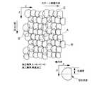
図5は、本発明の反射体10を上面から見た平面図である。反射体10は、1辺が規定単位Mで示される領域でランダムなサイズの凹部13がランダムに配置されている。この一辺が規定単位Mの領域の凹部13の集まりである反射体小片41が繰り返し形成されて、大きな反射面42を構成する。 FIG. 5 is a plan view of the
規定単位Mの長さは、30〜3000μmに設定される。反射体小片41の一辺の長さである規定単位Mを30〜3000μmに設定することにより、反射体10を例えば液晶表示装置の反射体として用いたときに、モアレ(干渉縞)の発生を効果的に防止することができる。なお、反射体小片41の縦横それぞれの長さMは30〜3000μmの範囲で互いに異なっていてもよく、液晶表示パネルの周期性(カラーフィルタ、画素電極、コンタクトホール等)に合わせて、それぞれ適宜調節することができる。 The length of the prescribed unit M is set to 30 to 3000 μm. By setting the prescribed unit M, which is the length of one side of the reflector
規定単位Mが30μmよりも小さいと、凹部13の周期性と液晶表示パネルの周期性(カラーフィルタ、画素電極、コンタクトホール等)との間で生じるモアレが強くなることがある。一方、規定単位Mを3000μmよりも大きくすると、反射体10の凹部13を転写形成するための母型の製造に長期間(例えば数ヶ月)掛かるようになり、実用的に採用できる反射体10の製造法ではなくなってしまう。 When the prescribed unit M is smaller than 30 μm, moire generated between the periodicity of the
このように、反射体小片41の一辺の長さである規定単位Mを30〜3000μmに設定し、この反射体小片41を繰り返し形成して、大きな反射面42を構成することによって、液晶表示装置の反射体として用いたときに、モアレ(干渉縞)の発生を効果的に防止することができるとともに、反射体10の凹部13を転写形成するための母型の製造に要する時間を実用的な範囲に留めることができる。よって、モアレの生じない反射体10を短期間にローコストで製造することが可能になる。 In this way, the prescribed unit M, which is the length of one side of the
図6は、反射体10を構成する反射体小片41での凹部13の形成例を示した説明図である。この例では、A,B,C,Dの4種類の深さの凹部を圧子を用いてランダム形成している。この例で形成された凹部13の形状と座標を表1に示す。 FIG. 6 is an explanatory diagram showing an example of forming the

以上のような反射体10を用いた液晶表示装置の例を図7に示す。液晶表示装置50を構成する液晶表示パネル51は、液晶層52を挟持して対向する第1の基板53と第2の基板54をシール材55で接合一体化した液晶表示パネルであり、第1の基板53の液晶層52側には、電極層や配向膜を含み、液晶層52を駆動制御するための表示回路56が形成され、第2の基板54の液晶層52側には、電極層や配向膜を含み液晶層52を駆動制御するための表示回路57が積層形成されている。 An example of a liquid crystal display device using the
また、表示回路56と表示回路57との間には、この2つの表示回路56,57間に一定の間隔を保持するためのスペーサ部材58が多数形成されている。そして、第1の基板53と第2の基板54の間に、反射体10が形成される。また反射体10の上面には、オーバーコート層59が積層されている。 In addition, a large number of
このような構成により、反射体10は液晶表示パネル51に入射した外光Nを効率的に反射させ、液晶層52を明るく照らし出し、モアレの無い鮮明な画像を観察できる。 With such a configuration, the
10 反射体
11 基板
12 反射膜
13 凹部
50 液晶表示装置
51 液晶表示パネルDESCRIPTION OF
Claims (2)
Translated fromJapanese前記規定単位を30〜3000μmに設定し、この規定単位を1ピッチとして繰り返し多数の凹部を形成して、一辺が前記規定単位よりも大きな面に多数の凹部を形成したことを特徴とする反射体。A reflector having a substrate in which a large number of fine concave portions are formed in random sizes for each prescribed unit, and a reflective film formed on one surface of the substrate,
The reflector is characterized in that the prescribed unit is set to 30 to 3000 μm, the prescribed unit is set as one pitch, a large number of recessed portions are formed, and a plurality of recessed portions are formed on a surface whose one side is larger than the prescribed unit. .
Priority Applications (6)
| Application Number | Priority Date | Filing Date | Title |
|---|---|---|---|
| JP2004010428AJP2005202280A (en) | 2004-01-19 | 2004-01-19 | Reflector and liquid crystal display device |
| TW093137224ATWI277774B (en) | 2004-01-19 | 2004-12-02 | Reflector and liquid-crystal display |
| EP05250192AEP1555568A1 (en) | 2004-01-19 | 2005-01-14 | Reflector and liquid-crystal display |
| US11/036,675US20050157228A1 (en) | 2004-01-19 | 2005-01-14 | Reflector and liquid-crystal display |
| CNA2005100045060ACN1645207A (en) | 2004-01-19 | 2005-01-18 | Reflector and liquid-crystal display |
| KR1020050004382AKR100644417B1 (en) | 2004-01-19 | 2005-01-18 | Reflector and liquid crystal display |
Applications Claiming Priority (1)
| Application Number | Priority Date | Filing Date | Title |
|---|---|---|---|
| JP2004010428AJP2005202280A (en) | 2004-01-19 | 2004-01-19 | Reflector and liquid crystal display device |
Publications (1)
| Publication Number | Publication Date |
|---|---|
| JP2005202280Atrue JP2005202280A (en) | 2005-07-28 |
Family
ID=34616937
Family Applications (1)
| Application Number | Title | Priority Date | Filing Date |
|---|---|---|---|
| JP2004010428AWithdrawnJP2005202280A (en) | 2004-01-19 | 2004-01-19 | Reflector and liquid crystal display device |
Country Status (6)
| Country | Link |
|---|---|
| US (1) | US20050157228A1 (en) |
| EP (1) | EP1555568A1 (en) |
| JP (1) | JP2005202280A (en) |
| KR (1) | KR100644417B1 (en) |
| CN (1) | CN1645207A (en) |
| TW (1) | TWI277774B (en) |
Cited By (1)
| Publication number | Priority date | Publication date | Assignee | Title |
|---|---|---|---|---|
| JP2007139897A (en)* | 2005-11-15 | 2007-06-07 | Alps Electric Co Ltd | Reflection member and liquid crystal display device using same |
Families Citing this family (1)
| Publication number | Priority date | Publication date | Assignee | Title |
|---|---|---|---|---|
| CN116068801B (en)* | 2023-03-02 | 2024-09-24 | 深圳市易快来科技股份有限公司 | High-reflectivity color reflective liquid crystal display screen and reflective display method |
Family Cites Families (5)
| Publication number | Priority date | Publication date | Assignee | Title |
|---|---|---|---|---|
| DE69220643T2 (en)* | 1991-09-10 | 1998-01-22 | Sharp Kk | Reflection type liquid crystal display device and method of manufacturing the same |
| US6130736A (en)* | 1997-06-13 | 2000-10-10 | Alps Electric Co., Ltd. | Liquid crystal display with corrugated reflective surface |
| TW594218B (en)* | 2000-07-03 | 2004-06-21 | Alps Electric Co Ltd | Reflector and reflective liquid crystal display device |
| TW538275B (en)* | 2000-09-18 | 2003-06-21 | Alps Electric Co Ltd | Reflective liquid crystal display device |
| KR100737895B1 (en)* | 2002-09-18 | 2007-07-10 | 삼성전자주식회사 | Reflective and reflective-transmissive liquid crystal display and manufacturing method thereof |
- 2004
- 2004-01-19JPJP2004010428Apatent/JP2005202280A/ennot_activeWithdrawn
- 2004-12-02TWTW093137224Apatent/TWI277774B/ennot_activeIP Right Cessation
- 2005
- 2005-01-14USUS11/036,675patent/US20050157228A1/ennot_activeAbandoned
- 2005-01-14EPEP05250192Apatent/EP1555568A1/ennot_activeWithdrawn
- 2005-01-18KRKR1020050004382Apatent/KR100644417B1/ennot_activeExpired - Fee Related
- 2005-01-18CNCNA2005100045060Apatent/CN1645207A/enactivePending
Cited By (1)
| Publication number | Priority date | Publication date | Assignee | Title |
|---|---|---|---|---|
| JP2007139897A (en)* | 2005-11-15 | 2007-06-07 | Alps Electric Co Ltd | Reflection member and liquid crystal display device using same |
Also Published As
| Publication number | Publication date |
|---|---|
| KR100644417B1 (en) | 2006-11-10 |
| CN1645207A (en) | 2005-07-27 |
| US20050157228A1 (en) | 2005-07-21 |
| TW200525187A (en) | 2005-08-01 |
| KR20050076635A (en) | 2005-07-26 |
| TWI277774B (en) | 2007-04-01 |
| EP1555568A1 (en) | 2005-07-20 |
Similar Documents
| Publication | Publication Date | Title |
|---|---|---|
| CN102287690B (en) | Backlight module | |
| CN101600987B (en) | Liquid crystal display device | |
| CN101589331B (en) | Liquid crystal display device | |
| KR101300035B1 (en) | An array substrate for reflective and trans-flective type liquid crystal display device and method of fabricating the same | |
| JPWO2009001508A1 (en) | Liquid crystal display device and method of manufacturing liquid crystal display device | |
| JP2005114772A (en) | Reflector and liquid crystal display device using the same | |
| JPWO2008047517A1 (en) | Liquid crystal display device and method of manufacturing liquid crystal display device | |
| CN110941116B (en) | Backlight module and manufacturing method thereof, and display device | |
| CN101059612B (en) | Method for manufacturing semi-transmissive and semi-reflective liquid crystal panel and active element array substrate | |
| KR100938162B1 (en) | Prism sheet and optical film having the same | |
| JP2005202280A (en) | Reflector and liquid crystal display device | |
| JP2007242410A (en) | Lighting device, electro-optical device, and manufacturing method therefor | |
| JP4903807B2 (en) | Liquid crystal display device and method of manufacturing liquid crystal display device | |
| US20080094538A1 (en) | Reflecting plate and liquid crystal display apparatus | |
| CN100559216C (en) | Reflective structure with diffuse directional reflection and device with such a structure | |
| TW200424683A (en) | Reflector and LCD device | |
| TWM336439U (en) | Diffuser capable of light condensing | |
| JP4061923B2 (en) | Transflective liquid crystal display device and manufacturing method thereof | |
| US7986385B2 (en) | LCD panel | |
| CN110993622A (en) | Array substrate, preparation method thereof and display panel | |
| KR200413319Y1 (en) | Light guide plate of liquid crystal display device | |
| JP4396249B2 (en) | Liquid crystal display | |
| JP2003140136A (en) | Liquid crystal display device and method for forming its light scattering face | |
| TWI266934B (en) | Reflector and liquid crystal display device using the same | |
| TW567350B (en) | Method for repairing of image display apparatus, film for repairing, and image display apparatus |
Legal Events
| Date | Code | Title | Description |
|---|---|---|---|
| A621 | Written request for application examination | Free format text:JAPANESE INTERMEDIATE CODE: A621 Effective date:20060906 | |
| A521 | Written amendment | Free format text:JAPANESE INTERMEDIATE CODE: A821 Effective date:20060907 | |
| A977 | Report on retrieval | Free format text:JAPANESE INTERMEDIATE CODE: A971007 Effective date:20090520 | |
| A131 | Notification of reasons for refusal | Free format text:JAPANESE INTERMEDIATE CODE: A131 Effective date:20090526 | |
| A761 | Written withdrawal of application | Free format text:JAPANESE INTERMEDIATE CODE: A761 Effective date:20090619 |