JP2005195854A - Image display device and inspection method thereof - Google Patents
Image display device and inspection method thereofDownload PDFInfo
- Publication number
- JP2005195854A JP2005195854AJP2004001882AJP2004001882AJP2005195854AJP 2005195854 AJP2005195854 AJP 2005195854AJP 2004001882 AJP2004001882 AJP 2004001882AJP 2004001882 AJP2004001882 AJP 2004001882AJP 2005195854 AJP2005195854 AJP 2005195854A
- Authority
- JP
- Japan
- Prior art keywords
- potential
- circuit
- electrode
- transistor
- node
- Prior art date
- Legal status (The legal status is an assumption and is not a legal conclusion. Google has not performed a legal analysis and makes no representation as to the accuracy of the status listed.)
- Withdrawn
Links
Images


Classifications
- G—PHYSICS
- G09—EDUCATION; CRYPTOGRAPHY; DISPLAY; ADVERTISING; SEALS
- G09G—ARRANGEMENTS OR CIRCUITS FOR CONTROL OF INDICATING DEVICES USING STATIC MEANS TO PRESENT VARIABLE INFORMATION
- G09G3/00—Control arrangements or circuits, of interest only in connection with visual indicators other than cathode-ray tubes
- G09G3/20—Control arrangements or circuits, of interest only in connection with visual indicators other than cathode-ray tubes for presentation of an assembly of a number of characters, e.g. a page, by composing the assembly by combination of individual elements arranged in a matrix no fixed position being assigned to or needed to be assigned to the individual characters or partial characters
- G09G3/22—Control arrangements or circuits, of interest only in connection with visual indicators other than cathode-ray tubes for presentation of an assembly of a number of characters, e.g. a page, by composing the assembly by combination of individual elements arranged in a matrix no fixed position being assigned to or needed to be assigned to the individual characters or partial characters using controlled light sources
- G09G3/30—Control arrangements or circuits, of interest only in connection with visual indicators other than cathode-ray tubes for presentation of an assembly of a number of characters, e.g. a page, by composing the assembly by combination of individual elements arranged in a matrix no fixed position being assigned to or needed to be assigned to the individual characters or partial characters using controlled light sources using electroluminescent panels
- G09G3/32—Control arrangements or circuits, of interest only in connection with visual indicators other than cathode-ray tubes for presentation of an assembly of a number of characters, e.g. a page, by composing the assembly by combination of individual elements arranged in a matrix no fixed position being assigned to or needed to be assigned to the individual characters or partial characters using controlled light sources using electroluminescent panels semiconductive, e.g. using light-emitting diodes [LED]
- G—PHYSICS
- G09—EDUCATION; CRYPTOGRAPHY; DISPLAY; ADVERTISING; SEALS
- G09G—ARRANGEMENTS OR CIRCUITS FOR CONTROL OF INDICATING DEVICES USING STATIC MEANS TO PRESENT VARIABLE INFORMATION
- G09G3/00—Control arrangements or circuits, of interest only in connection with visual indicators other than cathode-ray tubes
- G09G3/006—Electronic inspection or testing of displays and display drivers, e.g. of LED or LCD displays
- G—PHYSICS
- G09—EDUCATION; CRYPTOGRAPHY; DISPLAY; ADVERTISING; SEALS
- G09G—ARRANGEMENTS OR CIRCUITS FOR CONTROL OF INDICATING DEVICES USING STATIC MEANS TO PRESENT VARIABLE INFORMATION
- G09G2300/00—Aspects of the constitution of display devices
- G09G2300/08—Active matrix structure, i.e. with use of active elements, inclusive of non-linear two terminal elements, in the pixels together with light emitting or modulating elements
- G09G2300/0809—Several active elements per pixel in active matrix panels
- G09G2300/0819—Several active elements per pixel in active matrix panels used for counteracting undesired variations, e.g. feedback or autozeroing
- G—PHYSICS
- G09—EDUCATION; CRYPTOGRAPHY; DISPLAY; ADVERTISING; SEALS
- G09G—ARRANGEMENTS OR CIRCUITS FOR CONTROL OF INDICATING DEVICES USING STATIC MEANS TO PRESENT VARIABLE INFORMATION
- G09G2300/00—Aspects of the constitution of display devices
- G09G2300/08—Active matrix structure, i.e. with use of active elements, inclusive of non-linear two terminal elements, in the pixels together with light emitting or modulating elements
- G09G2300/0809—Several active elements per pixel in active matrix panels
- G09G2300/0833—Several active elements per pixel in active matrix panels forming a linear amplifier or follower
- G09G2300/0838—Several active elements per pixel in active matrix panels forming a linear amplifier or follower with level shifting
- G—PHYSICS
- G09—EDUCATION; CRYPTOGRAPHY; DISPLAY; ADVERTISING; SEALS
- G09G—ARRANGEMENTS OR CIRCUITS FOR CONTROL OF INDICATING DEVICES USING STATIC MEANS TO PRESENT VARIABLE INFORMATION
- G09G2300/00—Aspects of the constitution of display devices
- G09G2300/08—Active matrix structure, i.e. with use of active elements, inclusive of non-linear two terminal elements, in the pixels together with light emitting or modulating elements
- G09G2300/0809—Several active elements per pixel in active matrix panels
- G09G2300/0842—Several active elements per pixel in active matrix panels forming a memory circuit, e.g. a dynamic memory with one capacitor
- G09G2300/0852—Several active elements per pixel in active matrix panels forming a memory circuit, e.g. a dynamic memory with one capacitor being a dynamic memory with more than one capacitor
- G—PHYSICS
- G09—EDUCATION; CRYPTOGRAPHY; DISPLAY; ADVERTISING; SEALS
- G09G—ARRANGEMENTS OR CIRCUITS FOR CONTROL OF INDICATING DEVICES USING STATIC MEANS TO PRESENT VARIABLE INFORMATION
- G09G2310/00—Command of the display device
- G09G2310/02—Addressing, scanning or driving the display screen or processing steps related thereto
- G09G2310/0264—Details of driving circuits
- G09G2310/0275—Details of drivers for data electrodes, other than drivers for liquid crystal, plasma or OLED displays, not related to handling digital grey scale data or to communication of data to the pixels by means of a current
- G—PHYSICS
- G09—EDUCATION; CRYPTOGRAPHY; DISPLAY; ADVERTISING; SEALS
- G09G—ARRANGEMENTS OR CIRCUITS FOR CONTROL OF INDICATING DEVICES USING STATIC MEANS TO PRESENT VARIABLE INFORMATION
- G09G2320/00—Control of display operating conditions
- G09G2320/02—Improving the quality of display appearance
- G09G2320/0233—Improving the luminance or brightness uniformity across the screen
- G—PHYSICS
- G09—EDUCATION; CRYPTOGRAPHY; DISPLAY; ADVERTISING; SEALS
- G09G—ARRANGEMENTS OR CIRCUITS FOR CONTROL OF INDICATING DEVICES USING STATIC MEANS TO PRESENT VARIABLE INFORMATION
- G09G2330/00—Aspects of power supply; Aspects of display protection and defect management
- G09G2330/02—Details of power systems and of start or stop of display operation
- G09G2330/021—Power management, e.g. power saving
- G—PHYSICS
- G09—EDUCATION; CRYPTOGRAPHY; DISPLAY; ADVERTISING; SEALS
- G09G—ARRANGEMENTS OR CIRCUITS FOR CONTROL OF INDICATING DEVICES USING STATIC MEANS TO PRESENT VARIABLE INFORMATION
- G09G3/00—Control arrangements or circuits, of interest only in connection with visual indicators other than cathode-ray tubes
- G09G3/20—Control arrangements or circuits, of interest only in connection with visual indicators other than cathode-ray tubes for presentation of an assembly of a number of characters, e.g. a page, by composing the assembly by combination of individual elements arranged in a matrix no fixed position being assigned to or needed to be assigned to the individual characters or partial characters
- G09G3/22—Control arrangements or circuits, of interest only in connection with visual indicators other than cathode-ray tubes for presentation of an assembly of a number of characters, e.g. a page, by composing the assembly by combination of individual elements arranged in a matrix no fixed position being assigned to or needed to be assigned to the individual characters or partial characters using controlled light sources
- G09G3/30—Control arrangements or circuits, of interest only in connection with visual indicators other than cathode-ray tubes for presentation of an assembly of a number of characters, e.g. a page, by composing the assembly by combination of individual elements arranged in a matrix no fixed position being assigned to or needed to be assigned to the individual characters or partial characters using controlled light sources using electroluminescent panels
- G09G3/32—Control arrangements or circuits, of interest only in connection with visual indicators other than cathode-ray tubes for presentation of an assembly of a number of characters, e.g. a page, by composing the assembly by combination of individual elements arranged in a matrix no fixed position being assigned to or needed to be assigned to the individual characters or partial characters using controlled light sources using electroluminescent panels semiconductive, e.g. using light-emitting diodes [LED]
- G09G3/3208—Control arrangements or circuits, of interest only in connection with visual indicators other than cathode-ray tubes for presentation of an assembly of a number of characters, e.g. a page, by composing the assembly by combination of individual elements arranged in a matrix no fixed position being assigned to or needed to be assigned to the individual characters or partial characters using controlled light sources using electroluminescent panels semiconductive, e.g. using light-emitting diodes [LED] organic, e.g. using organic light-emitting diodes [OLED]
- G09G3/3225—Control arrangements or circuits, of interest only in connection with visual indicators other than cathode-ray tubes for presentation of an assembly of a number of characters, e.g. a page, by composing the assembly by combination of individual elements arranged in a matrix no fixed position being assigned to or needed to be assigned to the individual characters or partial characters using controlled light sources using electroluminescent panels semiconductive, e.g. using light-emitting diodes [LED] organic, e.g. using organic light-emitting diodes [OLED] using an active matrix
- G09G3/3233—Control arrangements or circuits, of interest only in connection with visual indicators other than cathode-ray tubes for presentation of an assembly of a number of characters, e.g. a page, by composing the assembly by combination of individual elements arranged in a matrix no fixed position being assigned to or needed to be assigned to the individual characters or partial characters using controlled light sources using electroluminescent panels semiconductive, e.g. using light-emitting diodes [LED] organic, e.g. using organic light-emitting diodes [OLED] using an active matrix with pixel circuitry controlling the current through the light-emitting element
Landscapes
- Engineering & Computer Science (AREA)
- Physics & Mathematics (AREA)
- Computer Hardware Design (AREA)
- General Physics & Mathematics (AREA)
- Theoretical Computer Science (AREA)
- Control Of Indicators Other Than Cathode Ray Tubes (AREA)
- Electroluminescent Light Sources (AREA)
- Control Of El Displays (AREA)
Abstract
Translated fromJapaneseDescription
Translated fromJapaneseこの発明は画像表示装置およびその検査方法に関し、特に、エレクトロルミネッセンス(以下、ELと称す)素子のような電界発光素子を備えた画像表示装置と、その検査方法に関する。 The present invention relates to an image display device and an inspection method thereof, and more particularly to an image display device including an electroluminescence element such as an electroluminescence (hereinafter referred to as EL) element and an inspection method thereof.
従来のEL表示装置では、各画素において、駆動トランジスタとEL素子を電源電位のラインと接地電位のラインとの間に直列接続するとともに、データ線と駆動トランジスタのゲートとの間にアクセストランジスタを接続し、データ線およびアクセストランジスタを介して駆動トランジスタのゲートに表示データに応じた電位を与え、その電位に応じた値の電流を駆動トランジスタおよびEL素子に流す。EL素子は、電流値に応じた光強度で発光する(たとえば特許文献1参照)。
このようなEL表示装置において駆動トランジスタを多結晶シリコン薄膜トランジスタで構成した場合、駆動トランジスタの特性(しきい値電圧、移動度)のばらつきが比較的大きくなり、これに応じてEL素子に流れる電流もばらつく。このため、同一の電位を複数の画素に書き込んだ場合でも画素毎に異なった色が表示され、特に隣接画素間における色のばらつきが目立つという問題があった。 In such an EL display device, when the driving transistor is composed of a polycrystalline silicon thin film transistor, the characteristics of the driving transistor (threshold voltage, mobility) are relatively large, and the current flowing through the EL element accordingly It varies. For this reason, even when the same potential is written to a plurality of pixels, a different color is displayed for each pixel, and there is a problem that color variation is particularly conspicuous between adjacent pixels.
それゆえに、この発明の主たる目的は、画素間の表示特性のばらつきが小さな画像表示装置とその検査方法を提供することである。 Therefore, a main object of the present invention is to provide an image display device in which variations in display characteristics between pixels are small and an inspection method thereof.
この発明に係る画像表示装置は、画像信号に従って画像を表示する画像表示装置であって、複数行複数列に配置され、各々が電界発光素子を含む複数の画素表示回路と、それぞれ複数列に対応して設けられた複数のデータ線と、画像信号に同期して複数行の各々を所定時間ずつ順次選択する垂直走査回路と、垂直走査回路によって1つの行が選択されている間に、複数のデータ線の各々に画像信号に応じた電位を与える水平走査回路とを備えたものである。ここで、各画素表示回路は、第1の電位のラインと制御ノードとの間に対応の電界発光素子と直列接続された第1のトランジスタと、制御ノードと第2の電位のラインとの間に接続された抵抗素子とを含み、制御ノードの電位に応じた値の電流を対応の電界発光素子に流す駆動回路と、垂直走査回路によって対応の行が選択されたことに応じて活性化され、制御ノードの電位が入力ノードの電位に一致するように第1のトランジスタの制御電極の電位を設定する差動増幅回路と、差動増幅回路が活性化されている期間内に活性化されて差動増幅回路のオフセット電圧を検出し、検出したオフセット電圧を対応のデータ線の電位に加算した電位を差動増幅回路の入力ノードに与え、差動増幅回路のオフセット電圧をキャンセルするオフセット補償回路とを備えている。 An image display device according to the present invention is an image display device that displays an image according to an image signal, and is arranged in a plurality of rows and a plurality of columns, each of which includes a plurality of pixel display circuits each including an electroluminescent element, each corresponding to a plurality of columns. A plurality of data lines, a vertical scanning circuit that sequentially selects each of a plurality of rows in synchronization with an image signal for a predetermined time, and a plurality of rows while a single row is selected by the vertical scanning circuit. And a horizontal scanning circuit for applying a potential corresponding to the image signal to each of the data lines. Here, each pixel display circuit includes a first transistor connected in series with a corresponding electroluminescent element between the first potential line and the control node, and between the control node and the second potential line. Is activated in response to selection of a corresponding row by a vertical scanning circuit and a driving circuit that passes a current corresponding to the potential of the control node to the corresponding electroluminescent element. A differential amplifier circuit that sets the potential of the control electrode of the first transistor so that the potential of the control node matches the potential of the input node, and the differential amplifier circuit is activated during the period in which the differential amplifier circuit is activated. Offset compensation that detects the offset voltage of the differential amplifier circuit, applies the potential obtained by adding the detected offset voltage to the potential of the corresponding data line to the input node of the differential amplifier circuit, and cancels the offset voltage of the differential amplifier circuit. And a circuit.
また、この発明に係る画像表示装置の検査方法は、上記画像表示装置を検査する検査方法であって、検査対象の画素表示回路に対応するデータ線にテスト電位を与え、画素表示回路の差動増幅回路およびオフセット補償回路を活性化させ、画素表示回路の制御ノードの電位を対応のデータ線を介して読出し、読出した電位に基づいて画素表示回路が正常か否かを判定する。 An inspection method for an image display device according to the present invention is an inspection method for inspecting the image display device, wherein a test potential is applied to a data line corresponding to a pixel display circuit to be inspected, and a differential of the pixel display circuit is provided. The amplifier circuit and the offset compensation circuit are activated, the potential of the control node of the pixel display circuit is read through the corresponding data line, and it is determined whether or not the pixel display circuit is normal based on the read potential.
この発明に係る画像表示装置では、電界発光素子に流れる電流は、制御ノードの電位と抵抗素子の抵抗値によって決定される。制御ノードの電位は、差動増幅回路およびオフセット補償回路によってデータ線の電位に等しい電位に設定される。したがって、電界発光素子に流れる電流値のばらつきの要因は、抵抗素子の抵抗値のみとなる。抵抗素子の抵抗値のばらつきは、トランジスタの特性(しきい値、移動度)のばらつきよりも小さいので、画素間の表示特性のばらつきは従来よりも小さくなる。また、垂直走査回路によって対応の行が選択されたときに差動増幅回路およびオフセット補償回路を活性化させるので、消費電流が小さくて済む。 In the image display device according to the present invention, the current flowing through the electroluminescent element is determined by the potential of the control node and the resistance value of the resistive element. The potential of the control node is set to a potential equal to the potential of the data line by the differential amplifier circuit and the offset compensation circuit. Accordingly, only the resistance value of the resistance element is the cause of the variation in the current value flowing through the electroluminescence element. Since the variation in resistance value of the resistance element is smaller than the variation in transistor characteristics (threshold value, mobility), the variation in display characteristics between pixels is smaller than in the past. In addition, since the differential amplifier circuit and the offset compensation circuit are activated when the corresponding row is selected by the vertical scanning circuit, current consumption can be reduced.
また、この発明に係る画像表示装置の検査方法では、検査対象の画素表示回路に対応するデータ線にテスト電位を与え、その画素表示回路の差動増幅回路およびオフセット補償回路を活性化させて上記制御ノードの電位を対応のデータ線を介して読出し、読出した電位に基づいてその画素表示回路が正常か否かを判定する。したがって、電界発光素子の光学特性を検査することなく画素表示回路を電気的に検査することができ、検査コストの低減化を図ることができる。 In the inspection method for an image display device according to the present invention, a test potential is applied to the data line corresponding to the pixel display circuit to be inspected, and the differential amplifier circuit and the offset compensation circuit of the pixel display circuit are activated to The potential of the control node is read through the corresponding data line, and it is determined whether or not the pixel display circuit is normal based on the read potential. Therefore, the pixel display circuit can be electrically inspected without inspecting the optical characteristics of the electroluminescent element, and the inspection cost can be reduced.
[実施の形態1]
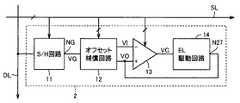
図1は、この発明の実施の形態1によるEL表示装置の構成を示すブロック図である。図1において、このEL表示装置は、画素アレイ1、垂直走査回路3および水平走査回路4を備える。画素アレイ1、垂直走査回路3および水平走査回路4が1枚の基板上に設けられていてもよいし、垂直走査回路3および水平走査回路4の一部または全部が外部回路として設けられていてもよい。[Embodiment 1]
FIG. 1 is a block diagram showing a configuration of an EL display device according to
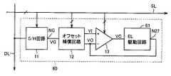
画素アレイ1は、複数行複数列に配置された複数の画素表示回路2と、それぞれ複数列に対応して設けられた複数のデータ線DLと、各行に対応して設けられた複数の信号線SLとを含む。各画素表示回路2は、EL素子を有し、対応の複数の信号線SLを介して与えられる複数の制御信号によって制御され、対応のデータ線DLを介して与えられる電位に応じた光強度で発光する。画素表示回路2については、後に詳述する。 The
垂直走査回路3は、画像信号に同期して動作し、複数行を1水平期間ずつ順次選択し、選択した行の複数の信号線SLを介して各画素表示回路2を制御し、各画素表示回路2に対応のデータ線DLの電位を保持させる。 The
水平走査回路4は、垂直走査回路3によって1つの行が選択されている間に、画像信号に応じた電位を各データ線DLに与える。画像信号は、複数ビットたとえば6ビットのデータ信号D0〜D5を含む。データ信号D0〜D5は、各画素表示回路2に対応してシリアルに生成される。6ビットのデータ信号D0〜D5により、各画素表示回路2において26=64段階の階調表示が可能となる。さらに、R(Red)、G(Green)、B(Blue)の3つの画素表示回路2で1つのカラー表示単位を構成すれば、約26万色のカラー表示が可能となる。The
すなわち水平走査回路4は、シフトレジスタ5、データラッチ回路6,7、階調電位発生回路8、デコード回路9、および出力バッファ回路10を含む。シフトレジスタ5は、データ信号D0〜D5の設定が切換えられる所定周期に同期したタイミングで、データラッチ回路6に対してデータ信号D0〜D5の取込みを指示する。データラッチ回路6は、シリアルに生成される1行分のデータ信号D0〜D5を順に取込んで保持する。 That is, the
1行分のデータ信号D0〜D5がデータラッチ回路7に取込まれたタイミングで、ラッチ信号LTの活性化に応答して、データラッチ回路6にラッチされたデータ信号D0〜D5群は、データラッチ回路7に伝達される。階調電位発生回路8は、64段階の階調電位V1〜V64をデコード回路9に与える。 In response to activation of the latch signal LT at the timing when the data signals D0 to D5 for one row are taken into the
デコード回路9は、各列毎に、データラッチ回路7にラッチされたデータ信号D0〜D5に従って、64段階の階調電位V1〜V64のうちのいずれかの電位を選択し、選択した電位を出力バッファ回路10に与える。出力バッファ回路10は、各列毎に、データ線DLの電位がデコード回路9から与えられた階調電位と同じ電位になるようにデータ線DLに電流を供給する。 The decode circuit 9 selects any one of the 64 gradation potentials V1 to V64 according to the data signals D0 to D5 latched in the
垂直走査回路3および水平走査回路4によって画素アレイ1の各画素表示回路2に階調電位が書き込まれると、画素アレイ1には1つの画像が表示される。 When the gradation potential is written to each
図2は、画素表示回路2の構成を示すブロック図である。図2において、画素表示回路2は、サンプルホールド(S/H)回路11、オフセット補償回路12、差動増幅回路13、およびEL駆動回路14を含む。サンプルホールド回路11は、信号線SLを介して与えられる制御信号によって制御され、垂直走査回路3によって対応の行が選択されている期間に対応のデータ線DLの電位をサンプリングおよびホールドし、サンプリングおよびホールドした電位VGをオフセット補償回路12に与える。 FIG. 2 is a block diagram illustrating a configuration of the
オフセット補償回路12は、複数の信号線SLを介して与えられる複数の制御信号によって制御され、差動増幅回路13が活性化されている期間内に、差動増幅回路13のオフセット電圧VOFを検出し、検出したオフセット電圧VOFをサンプルホールド回路11から与えられた電位VGに加算した電位VI=VG+VOFを差動増幅回路13に与え、差動増幅回路13のオフセット電圧VOFをキャンセルする。 The offset
差動増幅回路13の反転入力端子(−)はオフセット補償回路12の出力電位VIを受け、その非反転入力端子(+)はEL駆動回路14の制御ノードN27の電位VOを受け、その出力端子はEL駆動回路14に接続される。差動増幅回路13は、複数の信号線SLを介して与えられる複数の制御信号に応答して活性化され、EL駆動回路14の制御ノードN27の電位VOがオフセット補償回路12から与えられた電位VIに一致するようにEL駆動回路14に制御電位VCを与える。EL駆動回路14は、差動増幅回路13から与えられた制御電位VCに応じた値の電流IELをEL素子に流してEL素子を発光させる。 The inverting input terminal (−) of the
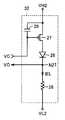
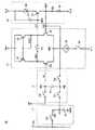
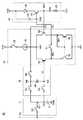
図3は、画素表示回路2の構成を詳細に示す回路図である。図3において、サンプルホールド回路11は、スイッチング素子SGおよびキャパシタ15を含む。スイッチング素子SGは、データ線DLとノードNGとの間に接続され、垂直走査回路3によって対応の行が選択されている期間にオンする。キャパシタ15は、ノードNGと接地電位GNDのラインとの間に接続される。スイッチング素子SGがオンすると、ノードNGがデータ線DLと同じ電位VGに充電される。スイッチング素子SGがオフされると、ノードNGの電位VGはキャパシタ15によって保持される。 FIG. 3 is a circuit diagram showing the configuration of the
EL駆動回路14は、高電位VH2のラインと制御ノードN27との間に直列接続されたEL素子26およびP型電界効果トランジスタ(以下、P型トランジスタと称す)27と、制御ノードN27と低電位VL2のラインとの間に接続された抵抗素子28と、高電位VH2のラインとP型トランジスタ27のゲート(ノードN29)の間に接続されたキャパシタ29とを含む。抵抗素子28の抵抗値をRとすると、EL素子26、P型トランジスタ27および抵抗素子28には制御ノードN27の電位VOと低電位VL2との間の電圧VO−VL2に応じた値の電流IEL=(VO−VL2)/Rが流れる。EL素子26は、電流IELに応じた光強度で発光する。 The
P型トランジスタ27のゲートN29の電位すなわち制御電位VCは、キャパシタ29によって保持される。キャパシタ29の一方電極は高電位VH2のラインに接続されているが、他の一定電位のラインに接続されていてもよい。また、ノードN29からのリーク電流が少ない場合は、キャパシタ29を除いてもよい。 The potential of the gate N29 of the P-
差動増幅回路13は、P型トランジスタ21,22、N型電界効果トランジスタ(以下、N型トランジスタと称す)23,24、定電流源25、およびスイッチング素子S1,S2を含む。P型トランジスタ21,22は、それぞれ高電位VH1のラインとノードN21,N22の間に接続され、それらのゲートはともにノードN22に接続される。P型トランジスタ21,22は、カレントミラー回路を構成する。スイッチング素子S1は、ノードN21とEL駆動回路14のノードN29との間に接続され、垂直走査回路3によって対応の行が選択されている期間内にオンする。 The
N型トランジスタ23,24は、それぞれノードN21,N22とノードN23との間に接続され、それらのゲートはそれぞれノードNA,N27に接続される。N型トランジスタ23,24のゲートは、それぞれ差動増幅回路13の反転入力端子および非反転入力端子を構成する。定電流源25およびスイッチング素子S2は、ノードN23と低電位VL1のラインとの間に直列接続される。スイッチング素子S2は、垂直走査回路3によって対応の行が選択されている期間内にオンする。スイッチング素子S2がオンすると、定電流源25は、ノードN23から低電位VL2のラインに所定の定電流を流す。 N-
スイッチング素子S2は、低消費電力化のために設けられており、電流を遮断することができれば、高電位VH1のラインと低電位VL1のラインとの間のいずれの位置に設けられていてもよい。たとえば、スイッチング素子S2をノードN23と定電流源25との間に設けてもよいし、高電位VH1のラインと、P型トランジスタ21,22のソースとの間に設けてもよい。また、VH1とVH2、VL1とVL2は、それぞれ同じ電位であってもよい。 The switching element S2 is provided for reducing power consumption, and may be provided at any position between the high potential VH1 line and the low potential VL1 line as long as the current can be cut off. . For example, the switching element S2 may be provided between the node N23 and the constant
次に、差動増幅回路13およびEL駆動回路14の動作について説明する。スイッチング素子S1,S2がオンすると、差動増幅回路13が活性化される。N型トランジスタ24には、制御ノードN27の電位VOに応じた値の電流が流れる。N型トランジスタ24とP型トランジスタ22は直列接続され、P型トランジスタ22と21はカレントミラー回路を構成するので、P型トランジスタ21にはN型トランジスタ24の電流に応じた値の電流が流れる。N型トランジスタ23には、ノードNAの電位VIに応じた値の電流が流れる。 Next, operations of the
VOがVIよりも高い場合は、P型トランジスタ21に流れる電流がN型トランジスタ23に流れる電流よりも大きくなって制御電位VCが上昇し、P型トランジスタ27に流れる電流が減少して制御ノードN27の電位VOが低下する。VOがVIよりも低い場合は、P型トランジスタ21に流れる電流がN型トランジスタ23に流れる電流よりも小さくなって制御電位VCが低下し、P型トランジスタ27に流れる電流が増加してVOが上昇する。 When VO is higher than VI, the current flowing through the P-
したがって、N型トランジスタ23のしきい値電圧VTN23とN型トランジスタ24のしきい値電圧VTN24とが等しい場合は、VO=VIとなる。しかし、N型トランジスタ23のしきい値電圧VTN23とN型トランジスタ24のしきい値電圧VTN24とが一致しない場合は、オフセット電圧VOF=VI−VO=VTN23−VTN24が発生する。たとえばVTN23がVTN24よりも高い場合、VOがVIよりも低い状態で差動増幅回路13が安定する。このオフセット電圧VOFは、オフセット補償回路12によって補償される。 Therefore, when the threshold voltage VTN23 of the N-
オフセット補償回路12は、スイッチング素子SA〜SCおよびキャパシタ16を含む。スイッチング素子SAはノードNGとNAの間に接続され、スイッチング素子SC,SBはノードNGとN27の間に直列接続される。キャパシタ16は、ノードNAと、スイッチング素子SB,SC間のノードNBとの間に接続される。 Offset
図4は、図1〜図3で示した画素表示回路2の動作を示すタイムチャートである。スイッチング素子SG,SA〜SC,S1,S2は、垂直走査回路3によって対応の行が選択されたときに、垂直走査回路3から対応の行の複数の信号線SLを介して与えられる複数の制御信号によってオン/オフ制御される。スイッチング素子SGは、垂直走査回路3によって対応の行が選択されている期間にオンされる。図4では、説明の便宜上スイッチング素子S1,S2,SA,SBが同時にオンされているが、以下に説明される動作が達成されれば同時にオンされる必要はない。また、データ線DLの電位の入力時刻は、時刻t0の前でも後でもよい。図4では、データ線DLの電位は既に入力されているものとする。 FIG. 4 is a time chart showing the operation of the
時刻t0においてスイッチング素子S1,S2,SA,SBがオンすると、ノードNGの電位VGがスイッチング素子SAを介してノードNAに伝達され、VI=VGとなる。また、駆動電流Iが流れて差動増幅回路13が活性化され、制御ノードN27の電位VOはVO=VG−VOFとなる。VOは、スイッチング素子SBを介してノードNBに伝達される。これにより、キャパシタ16は、VI−VO=VOFに充電される。 When switching elements S1, S2, SA, and SB are turned on at time t0, potential VG of node NG is transmitted to node NA via switching element SA, and VI = VG. In addition, the drive current I flows, the
時刻t1においてスイッチング素子SA,SBがオフした後、時刻t2においてスイッチング素子SCがオンすると、ノードNBの電位がVG−VOFからVGに変化する。この変化分VOFがキャパシタ16を介してノードNAに伝達され、ノードNAの電位VIがVI=VG+VOFとなる。この結果、制御ノードN27の電位VOがVO=VGとなり、オフセット電圧VOFがキャンセルされる。 After switching elements SA and SB are turned off at time t1, when switching element SC is turned on at time t2, the potential of node NB changes from VG-VOF to VG. This change VOF is transmitted to the node NA via the
このとき抵抗素子28には、電流IEL=(VG−VL2)/R=(VG/R)−(VL2/R)が流れる。R,VL2の各々を一定値にすると、IELはVGに比例する。特に、VL2が接地電位GNDの場合は、IEL=VG/Rとなる。Rを所定値に設定すれば、VGによりIELを決めることができる。つまり、VGによりEL素子26の輝度を制御することができる。 At this time, the current IEL = (VG−VL2) / R = (VG / R) − (VL2 / R) flows through the resistance element. When each of R and VL2 is a constant value, IEL is proportional to VG. In particular, when VL2 is the ground potential GND, IEL = VG / R. If R is set to a predetermined value, IEL can be determined by VG. That is, the luminance of the
ここで、IELがばらつく要因となるのは、Rのばらつきである。従来技術では駆動トランジスタのしきい値電圧と移動度の2つの要因がIELのばらつきの原因となっていたが、本願発明では抵抗素子28の抵抗値RのみがIELのばらつきの要因となる。したがって、従来技術よりもIELのばらつきの要因数が減少し、IELのばらつきが減少する。なお、画素表示回路2は、多結晶シリコン薄膜の表面に形成される。抵抗素子28の抵抗値Rは、多結晶シリコン薄膜へのイオン注入量によって調整される。 Here, it is the variation of R that causes the IEL to vary. In the prior art, the two factors of the threshold voltage and mobility of the driving transistor cause the variation in IEL. In the present invention, only the resistance value R of the
また、EL表示装置では、IELが常時流れているので消費電流が大きくなる。EL表示装置の消費電流を小さくするためには、IELを低減化する必要がある。このため従来技術では、駆動トランジスタのゲート・ソース間電圧を駆動トランジスタのしきい値電圧に近づけて駆動トランジスタの相互コンダクタンスを下げる必要がある。ところがゲート・ソース間電圧を駆動トランジスタのしきい値電圧に近づける程、IELがしきい値電圧のばらつきの影響を受け易くなるので、従来は低消費電力化が困難であった。これに対して本願発明では、抵抗素子28の抵抗値Rを単純に大きくすればIELが小さくなるので、低消費電力化が容易である。 Further, in the EL display device, current consumption increases because IEL always flows. In order to reduce the current consumption of the EL display device, it is necessary to reduce the IEL. Therefore, in the prior art, it is necessary to reduce the mutual conductance of the drive transistor by bringing the gate-source voltage of the drive transistor close to the threshold voltage of the drive transistor. However, the closer the gate-source voltage is to the threshold voltage of the driving transistor, the more easily IEL is affected by variations in threshold voltage, and thus it has been difficult to reduce power consumption. On the other hand, in the present invention, if the resistance value R of the
図4に戻って、時刻t3においてスイッチング素子S1がオフすると、制御電位VCがキャパシタ29によって保持される。時刻t4において、スイッチング素子S2がオフすると、駆動電流Iが遮断されて差動増幅回路13が非活性化される。差動増幅回路13を非活性化させるのは、EL素子26を発光させるための電圧はキャパシタ29によって保持されているので、差動増幅回路13の動作は不要になるからである。差動増幅回路13の駆動電流Iは対応の行が選択されている期間内しか流れないので、差動増幅回路13を設けたことによる消費電流の増加は小さい。 Returning to FIG. 4, when switching element S <b> 1 is turned off at time t <b> 3, control potential VC is held by
なお、スイッチング素子S1,S2を同時にオフさせることも可能であるが、スイッチング素子S2のオフにより制御電位VCが変化し、変化後の電位がキャパシタ29に保持される可能性があるので、スイッチング素子S1をオフさせた後にスイッチング素子S2をオフさせている。 Although the switching elements S1 and S2 can be turned off at the same time, the control potential VC is changed by turning off the switching element S2, and the changed potential may be held in the
また、スイッチング素子S1をオフさせた後は、ノードN29から電荷がリークしてノードN29の電位VCが時間の経過とともに低下する。しかし、1フレーム時間(約16m秒)における電位VCの低下は、実用上問題ない。 Further, after the switching element S1 is turned off, the charge leaks from the node N29, and the potential VC of the node N29 decreases with time. However, there is no practical problem in reducing the potential VC in one frame time (about 16 milliseconds).
以下、この実施の形態1の種々の変更例について説明する。図5の変更例では、画素表示回路2のEL駆動回路14がEL駆動回路31で置換される。EL駆動回路31では、キャパシタ29は、P型トランジスタ27のゲート・ソース間に接続される。この変更例でも、実施の形態1と同じ効果が得られる。 Hereinafter, various modifications of the first embodiment will be described. In the modified example of FIG. 5, the
図6の変更例では、画素表示回路2のEL駆動回路14がEL駆動回路32で置換される。EL駆動回路32では、P型トランジスタ27およびEL素子26が高電位VH2のラインと制御ノードN27との間に接続され、キャパシタ29はP型トランジスタ27のゲート・ソース間に接続される。この変更例でも、実施の形態1と同じ効果が得られる。 In the modified example of FIG. 6, the
図7の変更例では、図3の定電流源25およびスイッチング素子S2がN型トランジスタ33およびスイッチ34で置換される。N型トランジスタ33はノードN23と低電位VL1のラインとの間に接続され、そのゲートはスイッチ34の共通端子34cに接続される。スイッチ34の一方端子34aはバイアス電位VBNを受け、その他方端子34bは低電位VL1のラインに接続される。図3のスイッチング素子S2がオンする期間(図4の時刻0〜t4)では、スイッチ34の端子34a,34c間が導通してN型トランジスタ33のゲートにバイアス電位VBNが与えられ、N型トランジスタ33は飽和領域で動作して定電流Iを流す。図3のスイッチング素子S2がオフする期間では、スイッチ34の端子34b,34c間が導通してN型トランジスタ33のゲートに低電位VL1が与えられ、N型トランジスタ33はオフする。この変更例でも、実施の形態1と同じ効果が得られる。 In the modification of FIG. 7, the constant
図8の変更例では、画素表示回路2が画素表示回路35で置換される。画素表示回路35では、スイッチング素子SAの一方電極がノードNGの代わりに基準電位VRのノードに接続される。基準電位VRは、電流供給能力が大きな外部電源あるいは内部電源から供給される。この場合は、キャパシタ16の充電が基準電位VRのノードを介して行なわれるので、図1の出力バッファ回路10の負荷が軽減され、オフセットキャンセル動作の高速化が図られる。 In the modification of FIG. 8, the
図3の画素表示回路2では、負帰還回路が構成されているので、発振動作が生じる可能性がある。発振動作を防止するため、位相補償が行なわれる。図9の画素表示回路36では、制御ノードN27と低電位VL3のラインとの間にキャパシタ37が接続される(支配極補償法)。図10の画素表示回路38では、キャパシタ37の一方電極は低電位VL3のラインの代わりに差動増幅回路13のノードN21に接続される(ミラー補償法)。図11の画素表示回路39では、制御ノードN27と低電位VL3のラインとの間に抵抗素子40およびキャパシタ37が接続される(ポール・ゼロ法)。これらの変更例では、発振動作が防止される。また、図3の画素表示回路2でも、動作条件によっては発振動作は生じない。 In the
[実施の形態2]
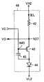
図12は、この発明の実施の形態2によるEL表示装置に含まれる画素表示回路40の構成を示す回路図であって、図3と対比される図である。図12を参照して、この画素表示回路40は、画素表示回路2のEL駆動回路14をEL駆動回路41で置換したものである。EL駆動回路41は、高電位VH2のラインと制御ノードN27との間に接続された抵抗素子42と、制御ノードN27と低電位VL2のラインとの間に直列接続されたN型トランジスタ43およびEL素子44と、N型トランジスタ43のゲートと低電位VL2のラインとの間に接続されたキャパシタ45とを含む。[Embodiment 2]
FIG. 12 is a circuit diagram showing the configuration of the
抵抗素子42の抵抗値をRとすると、抵抗素子42、N型トランジスタ43およびEL素子44には高電位VH2と制御ノードN27の電位VOとの間の電圧VH2-VOに応じた値の電流IEL=(VH2−VO)/Rが流れる。EL素子44は、電流IELに応じた光強度で発光する。 When the resistance value of the
N型トランジスタ43のゲート(ノードN45)の電位すなわち制御電位VCは、キャパシタ45によって保持される。キャパシタ45の一方電極は低電位VL2のラインに接続されているが、他の一定電位のラインに接続されていてもよい。また、ノードN45からのリーク電流が少ない場合は、キャパシタ45を除いてもよい。 The potential of the gate (node N45) of the N-
次に、差動増幅回路13およびEL駆動回路41の動作について説明する。スイッチング素子S1,S2がオンすると、差動増幅回路13が活性化される。N型トランジスタ24には、制御ノードN27の電位VOに応じた値の電流が流れる。N型トランジスタ24とP型トランジスタ22は直列接続され、P型トランジスタ22と21はカレントミラー回路を構成するので、P型トランジスタ21にはN型トランジスタ24の電流に応じた値の電流が流れる。N型トランジスタ23には、ノードNAの電位VIに応じた値の電流が流れる。 Next, operations of the
VOがVIよりも高い場合は、P型トランジスタ21に流れる電流がN型トランジスタ23に流れる電流よりも大きくなって制御電位VCが上昇し、N型トランジスタ43に流れる電流が増加して制御ノードN27の電位VOが低下する。VOがVIよりも低い場合は、P型トランジスタ21に流れる電流がN型トランジスタ23に流れる電流よりも小さくなって制御電位VCが低下し、N型トランジスタ43に流れる電流が減少してVOが上昇する。 When VO is higher than VI, the current flowing through the P-
したがって、N型トランジスタ23のしきい値電圧VTN23とN型トランジスタ24のしきい値電圧VTN24とが等しい場合は、VO=VIとなる。しかし、N型トランジスタ23のしきい値電圧VTN23とN型トランジスタ24のしきい値電圧VTN24とが一致しない場合は、オフセット電圧VOF=VI−VO=VTN23−VTN24が発生する。たとえばVTN23がVTN24よりも高い場合、VOがVIよりも低い状態で差動増幅回路13が安定する。このオフセット電圧VOFは、オフセット補償回路12によって補償される。 Therefore, when the threshold voltage VTN23 of the N-
この実施の形態2でも、実施の形態1と同じ効果が得られる。 Also in this second embodiment, the same effect as in the first embodiment can be obtained.
以下、この実施の形態2の種々の変更例について説明する。図13の変更例では、EL駆動回路41がEL駆動回路46で置換される。EL駆動回路46では、キャパシタ45は、N型トランジスタ43のゲート・ソース間に接続される。図14の変更例では、EL駆動回路41がEL駆動回路47で置換される。EL駆動回路47では、EL素子44およびN型トランジスタ43が制御ノードN27と低電位VL2のラインとの間に直列接続され、キャパシタ45はN型トランジスタ43のゲート・ソース間に接続される。これらの変更例でも、実施の形態2と同じ効果が得られる。 Hereinafter, various modifications of the second embodiment will be described. In the modified example of FIG. 13, the
[実施の形態3]
図15は、この発明の実施の形態3によるEL表示装置に含まれる画素表示回路50の構成を示す回路図であって、図3と対比される図である。図15を参照して、この画素表示回路50は、画素表示回路2の差動増幅回路13を差動増幅回路51で置換したものである。[Embodiment 3]
FIG. 15 is a circuit diagram showing a configuration of a
差動増幅回路51は、スイッチング素子S1,S2、定電流源52、P型トランジスタ53,54およびN型トランジスタ55,56を含む。スイッチング素子S2および定電流源52は、高電位VH1のラインとノードN52の間に接続される。スイッチング素子S2がオンすると、定電流源52は、高電位VH1のラインからノードN52に所定の定電流を流す。P型トランジスタ53,54は、それぞれノードN52とノードN53,N54の間に接続され、それらのゲートはそれぞれノードNA,N27に接続される。P型トランジスタ53,54のゲートは、それぞれ差動増幅回路51の反転入力端子および非反転入力端子を構成する。スイッチング素子S1は、ノードN53とP型トランジスタ27のゲートとの間に接続される。N型トランジスタ55,56は、それぞれノードN53,N54と低電位VL1のラインとの間に接続され、それらのゲートはともにノードN54に接続される。N型トランジスタ55,56は、カレントミラー回路を構成する。 The
次に、差動増幅回路51およびEL駆動回路14の動作について説明する。P型トランジスタ54には、制御ノードN27の電位VOに応じた値の電流が流れる。P型トランジスタ54とN型トランジスタ56は直列接続され、N型トランジスタ56と55はカレントミラー回路を構成するので、N型トランジスタ55にはP型トランジスタ54の電流に応じた値の電流が流れる。P型トランジスタ53には、ノードNAの電位VIに応じた値の電流が流れる。 Next, operations of the
VOがVIよりも高い場合は、N型トランジスタ55に流れる電流がP型トランジスタ53に流れる電流よりも小さくなって制御電位VCが上昇し、P型トランジスタ27に流れる電流が減少してVOが低下する。VOがVIよりも低い場合は、N型トランジスタ55に流れる電流がP型トランジスタ53に流れる電流よりも大きくなって制御電位VCが低下し、P型トランジスタ27に流れる電流が増加してVOが上昇する。 When VO is higher than VI, the current flowing through the N-
したがって、P型トランジスタ53のしきい値電圧VTP53とP型トランジスタ54のしきい値電圧VTP54とが等しい場合は、VOはVIに等しくなる。しかし、P型トランジスタ53のしきい値電圧VTP53とP型トランジスタ54のしきい値電圧VTP54とが一致しない場合は、オフセット電圧VOF=VI−VO=|VTP54|−|VTP53|が発生する。たとえば|VTP53|が|VTP54|よりも高い場合、VOがVIよりも高い状態で差動増幅回路51が安定する。このオフセット電圧VOFは、図4で示したオフセットキャンセル動作によって補償される。 Therefore, when the threshold voltage VTP53 of the P-
この実施の形態3でも、実施の形態2と同じ効果が得られる。 In the third embodiment, the same effect as in the second embodiment can be obtained.
次に、この実施の形態3の変更例について説明する。図16の変更例では、図5のスイッチング素子S2および定電流源52がP型トランジスタ57およびスイッチ58で置換される。P型トランジスタ57は高電位VH1のラインとノードN52との間に接続され、そのゲートはスイッチ58の共通端子58cに接続される。スイッチ58の一方端子58aはバイアス電位VBPを受け、その他方端子58bは高電位VH1のラインに接続される。図15のスイッチング素子S2がオンする期間(図4の時刻0〜t4)では、スイッチ58の端子58a,58c間が導通してN型トランジスタ57のゲートにバイアス電位VBPが与えられ、P型トランジスタ57は飽和領域で動作して定電流Iを流す。図15のスイッチング素子S2がオフする期間では、スイッチ58の端子58b,58c間が導通してN型トランジスタ57のゲートに高電位VH1が与えられ、P型トランジスタ57はオフする。この変更例でも、実施の形態3と同じ効果が得られる。 Next, a modified example of the third embodiment will be described. In the modification of FIG. 16, the switching element S <b> 2 and the constant
図17の画素表示回路59は、図15の画素表示回路50のEL駆動回路14を図12のEL駆動回路41で置換したものである。この変更例でも、実施の形態3と同じ効果が得られる。 The
[実施の形態4]
図18は、この発明の実施の形態4によるEL表示装置に含まれる画素表示回路60の構成を示すブロック図であって、図2と対比される図である。図2を参照して、この画素表示回路60が図2の画素表示回路2と異なる点は、EL駆動回路14がEL駆動回路61で置換され、EL駆動回路61の制御ノードN27が差動増幅回路13の反転入力端子(−)に接続され、オフセット補償回路12の出力電位VIが差動増幅回路13の非反転入力端子(+)に入力されている点である。[Embodiment 4]
FIG. 18 is a block diagram showing a configuration of a
図19は、図18に示した画素表示回路60の構成を詳細に示す回路図である。EL駆動回路61は、図3のEL駆動回路14のP型トランジスタ27をN型トランジスタ62で置換したものである。差動増幅回路13のN型トランジスタ23のゲート(反転入力端子)は制御ノードN27に接続され、N型トランジスタ24のゲート(非反転入力端子)はノードNAに接続され、ノードN21はスイッチング素子S1を介してN型トランジスタ62のゲートに接続される。 FIG. 19 is a circuit diagram showing in detail the configuration of the
次に、差動増幅回路13およびEL駆動回路61の動作について説明する。スイッチング素子S1,S2がオンすると、差動増幅回路13が活性化される。N型トランジスタ24には、ノードNAの電位VIに応じた値の電流が流れる。N型トランジスタ24とP型トランジスタ22は直列接続され、P型トランジスタ22と21はカレントミラー回路を構成するので、P型トランジスタ21にはN型トランジスタ24の電流に応じた値の電流が流れる。N型トランジスタ23には、制御ノードN27の電位VOに応じた値の電流が流れる。 Next, operations of the
VOがVIよりも高い場合は、P型トランジスタ21に流れる電流がN型トランジスタ23に流れる電流よりも小さくなって制御電位VCが低下し、N型トランジスタ62に流れる電流が減少して制御ノードN27の電位VOが低下する。VOがVIよりも低い場合は、P型トランジスタ21に流れる電流がN型トランジスタ23に流れる電流よりも大きくなって制御電位VCが上昇し、N型トランジスタ62に流れる電流が増加してVOが低下する。 When VO is higher than VI, the current flowing through the P-
したがって、N型トランジスタ23のしきい値電圧VTN23とN型トランジスタ24のしきい値電圧VTN24とが等しい場合は、VO=VIとなる。しかし、N型トランジスタ23のしきい値電圧VTN23とN型トランジスタ24のしきい値電圧VTN24とが一致しない場合は、オフセット電圧VOF=VI−VO=VTN24−VTN23が発生する。たとえばVTN24がVTN23よりも高い場合、VOがVIよりも低い状態で差動増幅回路13が安定する。このオフセット電圧VOFは、オフセット補償回路12によって補償される。 Therefore, when the threshold voltage VTN23 of the N-
この実施の形態4では、EL駆動回路61はN型トランジスタ62を用いたソースフォロワ回路になっており、発振動作が生じ難い構成になっている。ただし、N型トランジスタ62のしきい値電圧分だけ高電位VH1を図3の場合よりも高くする必要がある。本発明では、垂直走査回路3によって対応の行が選択されていない場合は、スイッチング素子S2をオフして高電位VH1のラインと低電位VL1のラインとの間に流れる電流を遮断するので、高電位VH1を高くしたことによる消費電流の増大は小さい。 In the fourth embodiment, the
以下、この実施の形態4の種々の変更例について説明する。図20の画素表示回路65は、図19の画素表示回路60のEL駆動回路61をEL駆動回路66で置換したものである。EL駆動回路66は、図12のEL駆動回路41のN型トランジスタ43をP型トランジスタ67で置換したものである。 Hereinafter, various modifications of the fourth embodiment will be described. A
VOがVIよりも高い場合は、P型トランジスタ21に流れる電流がN型トランジスタ23に流れる電流よりも小さくなって制御電位VCが低下し、P型トランジスタ67に流れる電流が増加して制御ノードN27の電位VOが低下する。VOがVIよりも低い場合は、P型トランジスタ21に流れる電流がN型トランジスタ23に流れる電流よりも大きくなって制御電位VCが上昇し、P型トランジスタ67に流れる電流が増加してVOが低下する。したがって、N型トランジスタ23のしきい値電圧VTN23とN型トランジスタ24のしきい値電圧VTN24とが等しい場合は、VO=VIとなる。 When VO is higher than VI, the current flowing through the P-
この変更例では、EL駆動回路66はP型トランジスタ67を用いたソースフォロワ回路になっており、発振動作が生じ難い構成になっている。ただし、P型トランジスタ67のしきい値電圧分だけ低電位VL1を図3の場合よりも低くする必要がある。本発明では、垂直走査回路3によって対応の行が選択されていない場合は、スイッチング素子S2をオフして高電位VH1のラインと低電位VL1のラインとの間に流れる電流を遮断するので、低電位VL1を低くしたことによる消費電流の増大は小さい。 In this modified example, the
また、図21の画素表示回路70は、図19の画素表示回路60の差動増幅回路13を図15の差動増幅回路51で置換したものである。また、図22の画素表示回路71は、図20の画素表示回路60の差動増幅回路13を図15の差動増幅回路51で置換したものである。これらの変更例でも、発振動作が生じることを防止することができる。 21 is obtained by replacing the
[実施の形態5]
上記画素表示回路においてスイッチング素子S1は、実際には、N型トランジスタ、あるいはP型トランジスタ、あるいは並列接続されたN型トランジスタおよびP型トランジスタで構成される。スイッチング素子S1を構成するトランジスタがオフするとき、トランジスタのゲート・ドレイン間あるいはゲート・ソース間に存在する寄生容量により、制御電位VCが変化して所定の値からずれるという問題がある。このとき変化する電圧は、フィードスルー電圧と呼ばれる。たとえば図3のキャパシタ29は、フィードスルー電圧の低減化に一定の効果を発揮するが充分ではない。この実施の形態5では、この問題の解決が図られる。[Embodiment 5]
In the pixel display circuit, the switching element S1 is actually composed of an N-type transistor, a P-type transistor, or an N-type transistor and a P-type transistor connected in parallel. When the transistor constituting the switching element S1 is turned off, there is a problem that the control potential VC changes and deviates from a predetermined value due to parasitic capacitance existing between the gate and drain of the transistor or between the gate and source. The voltage that changes at this time is called a feedthrough voltage. For example, the
図23は、この発明の実施の形態5によるEL表示装置に含まれる画素表示回路75の構成を示す回路図であって、図19と対比される図である。図23を参照して、この画素表示回路75が図19の画素表示回路60と異なる点は、フィードスルー補償回路76が追加され、EL駆動回路61がEL駆動回路78で置換されている点である。 FIG. 23 is a circuit diagram showing a configuration of a
フィードスルー補償回路76は、スイッチング素子S3,S4およびキャパシタ77を含む。スイッチング素子S3,S4は、制御ノードN27とサンプルホールド回路11のノードNGとの間に直列接続される。スイッチング素子S3は、垂直走査回路3から信号線SLを介して与えられる制御信号によって制御され、スイッチング素子S1と同時にオン/オフする。スイッチング素子S4は、垂直走査回路3から信号線SLを介して与えられる制御信号によって制御され、スイッチング素子S1,S3がオフしたことに応じてオンする。キャパシタ77は、N型トランジスタ62のゲートと、スイッチング素子S3,S4間のノードN77との間に接続される。EL駆動回路78は、図19のEL駆動回路61からキャパシタ29を除去したものである。 The
図24は、フィードスルーキャンセル動作を示すタイムチャートである。図24において、時刻t0においてスイッチング素子S1,S3がともにオンし、図4で示したオフセットキャンセル動作が行なわれ、ノードN29に制御電位VCが与えられ、ノードN27,N77にVO=VGが与えられる。 FIG. 24 is a time chart showing the feedthrough cancel operation. 24, switching elements S1 and S3 are both turned on at time t0, the offset cancel operation shown in FIG. 4 is performed, control potential VC is applied to node N29, and VO = VG is applied to nodes N27 and N77. .
時刻t1においてスイッチング素子S1,S3がオフすると、スイッチング素子S1,S3によってフィードスルー電圧が発生する。今、スイッチング素子S1のみについて考える。スイッチング素子S1がオフしたことによりノードN29に−ΔV1のフィードスルー電圧が生じたとすると、ノードN29の電位VCがΔV1だけ低下する。キャパシタ77の容量値はノードN77の寄生容量値よりも充分に大きく設定されているので、この変化分はキャパシタ77によりノードN77にほぼ100%伝達される。同様に、スイッチング素子S3がオフしたことによりノードN77の電位VO=VGがΔV3だけ低下し、この変化分がノードN29にほぼ100%伝達される。最終的に、ノードN77の電位はVO=VGからΔV1+ΔV3だけ低下し、同様にノードN29の電位はVCからΔV1+ΔV3だけ低下する。 When switching elements S1 and S3 are turned off at time t1, a feedthrough voltage is generated by switching elements S1 and S3. Now consider only the switching element S1. If the feedthrough voltage of −ΔV1 is generated at the node N29 due to the switching element S1 being turned off, the potential VC of the node N29 decreases by ΔV1. Since the capacitance value of the
次に時刻t2においてスイッチング素子S4がオンすると、ノードN77の電位が低インピーダンス状態にあるノードNGの電位VGになる。つまり、ノードN77の電位がΔV1+ΔV3だけ上昇する。この変化分は、キャパシタ77を介してノードN29に伝達され、ノードN29の電位がVCに戻る。このようにしてフィードスルー電圧がキャンセルされる。 Next, when the switching element S4 is turned on at time t2, the potential of the node N77 becomes the potential VG of the node NG in the low impedance state. That is, the potential of the node N77 increases by ΔV1 + ΔV3. This change is transmitted to the node N29 via the
なお、キャパシタ77は、スイッチング素子S4がオンしている間は、その一方電極が一定電位VGに接続されているので、ノードN29の電位保持容量として機能する。
図25は、実施の形態5の変更例を示す回路図である。この画素表示回路80が図23の画素表示回路75と異なる点は、フィードスルー補償回路76がフィードスルー補償回路81で置換されている点である。フィードスルー補償回路81は、スイッチング素子S3,S4およびキャパシタ77を含む。スイッチング素子S3は、差動増幅回路13のN型トランジスタ23のゲートと制御ノードN27との間に接続される。スイッチング素子S4は、サンプルホールド回路11のノードNGとN型トランジスタ23のゲートとの間に接続される。キャパシタ77は、ノードN29とスイッチング素子S3,S4間のノードN77との間に接続される。この変更例では、EL駆動回路78から差動増幅回路13への帰還ルートの配線とスイッチング素子S3用の配線が共有されるので、図23の画素表示回路75に比べて回路の占有面積が低減される。ただし、N型トランジスタ23のゲート容量がノードN77の寄生容量として作用するというデメリットがある。 FIG. 25 is a circuit diagram showing a modification of the fifth embodiment. The
[実施の形態6]
本発明のEL表示装置を生産する場合、EL表示装置として組み立てたときの歩留り(良品率)が重要になる。EL表示装置の歩留りは、占有面積が大きな画素アレイ2の欠陥率で大部分が決まる。EL表示装置の製造コストを低減するためには、できるだけ製造工程の前段階で不良品を除去することが好ましい。つまり、EL表示装置として組立ててEL素子の表示特性を光学的に検査する段階で不良品を検出するよりも、画素表示回路が形成された段階で電気的な検査で不良品を検出した方が製造コストの低減化に有効である。この実施の形態6では、画素表示回路の電気的な検査方法について説明する。[Embodiment 6]
When producing the EL display device of the present invention, the yield (non-defective product rate) when assembled as an EL display device becomes important. The yield of the EL display device is largely determined by the defect rate of the
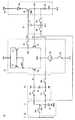
図26は、この発明の実施の形態6による画素表示回路2の検査方法を示す回路図である。図26において、この検査方法では、スイッチ85、ライトドライバ86およびセンスアンプ87が用いられる。スイッチ85の共通端子はデータ線DLに接続され、その一方端子85aはライトドライバ86の出力ノードに接続され、その他方端子はセンスアンプ87に接続される。 FIG. 26 is a circuit diagram showing an inspection method for the
まず、スイッチング素子SG,SA,SB,S1,S2をオンさせ、スイッチング素子SCをオフさせる。また、スイッチ85の端子85a,85c間を導通させ、ライトドライバ86の入力ノードに所定の電位VGを印加する。この結果、VI=VG、VO=VI−VOFとなる。 First, switching elements SG, SA, SB, S1, and S2 are turned on, and switching element SC is turned off. Further, the
次に、スイッチング素子SA,SBをオフにしてノードNAの電位VI=VGを保持する。次いでスイッチング素子SCをオンすると、ノードNBの電位がVOFだけ変化してノードNAの電位VIがVI=VG+VOFとなる。この結果、VO=VGとなる。次に、スイッチング素子S1,S2を順次オフする。以上は、図4で説明した動作と同じである。ただし、スイッチング素子S2は、オンのままでもよい。 Next, the switching elements SA and SB are turned off to hold the potential VI = VG of the node NA. Next, when the switching element SC is turned on, the potential of the node NB changes by VOF, and the potential VI of the node NA becomes VI = VG + VOF. As a result, VO = VG. Next, the switching elements S1 and S2 are sequentially turned off. The above is the same as the operation described in FIG. However, the switching element S2 may remain on.
次に、ライトドライバ86の入力ノードにVGとは異なる電位(たとえば接地電位GND)を印加してデータ線DLの電位をVGとは異なる電位に設定した後、スイッチ85の端子85b,85c間を導通させ、データ線DLをセンスアンプ87の入力ノードに接続する。 Next, a potential different from VG (for example, ground potential GND) is applied to the input node of the
次に、スイッチング素子SBをオンさせる。この結果、データ線DLには制御ノードN27の電位VOが伝達される。この電位VOをセンスアンプ87で読み取り、VO=VGの場合は画素表示回路2は正常であると判定し、VO≠VGの場合は画素表示回路2は不良であると判定する。 Next, the switching element SB is turned on. As a result, the potential VO of the control node N27 is transmitted to the data line DL. This potential VO is read by the
なお、この実施の形態6では、制御ノードN27の電位VOを読み出したが、制御ノードN27からデータ線DLに流れる電流を検出し、その検出結果に基づいて画素表示回路2の良否を判定しても良い。また、スイッチング素子SG,SA,SB,SC,S1,S2のオン/オフの組合せで、その他種々の検査方法が考えられる。 In the sixth embodiment, the potential VO of the control node N27 is read. However, the current flowing from the control node N27 to the data line DL is detected, and the quality of the
今回開示された実施の形態はすべての点で例示であって制限的なものではないと考えられるべきである。本発明の範囲は上記した説明ではなくて特許請求の範囲によって示され、特許請求の範囲と均等の意味および範囲内でのすべての変更が含まれることが意図される。 The embodiment disclosed this time should be considered as illustrative in all points and not restrictive. The scope of the present invention is defined by the terms of the claims, rather than the description above, and is intended to include any modifications within the scope and meaning equivalent to the terms of the claims.
1 画素アレイ、2,35,36,38,39,40,50,59,60,65,70,71,75,80 画素表示回路、DL データ線、SL 信号線、3 垂直走査回路、4 水平走査回路、5 シフトレジスタ、6,7 データラッチ回路、8 階調電位発生回路、9 デコード回路、10 出力バッファ回路、11 サンプルホールド回路、12 オフセット補償回路、13,51 差動増幅回路、14,31,32,41,46,47,61,66,78 EL駆動回路、SG,SA,SB,SC,S1〜S4 スイッチング素子、15,16,29,37,45,77 キャパシタ、21,22,27,53,54,57,67 P型トランジスタ、23,24,33,43,55,56,62 N型トランジスタ、25,52 定電流源、26,44 EL素子、28,40,42 抵抗素子、34,58,85 スイッチ、76,81 フィードスルー補償回路、86 ライトドライバ、87 センスアンプ。 1 pixel array, 2, 35, 36, 38, 39, 40, 50, 59, 60, 65, 70, 71, 75, 80 pixel display circuit, DL data line, SL signal line, 3 vertical scanning circuit, 4 horizontal Scan circuit, 5 shift register, 6, 7 data latch circuit, 8 gradation potential generation circuit, 9 decode circuit, 10 output buffer circuit, 11 sample hold circuit, 12 offset compensation circuit, 13, 51 differential amplifier circuit, 14, 31, 32, 41, 46, 47, 61, 66, 78 EL drive circuit, SG, SA, SB, SC, S1 to S4 switching elements, 15, 16, 29, 37, 45, 77 capacitors, 21, 22, 27, 53, 54, 57, 67 P-type transistor, 23, 24, 33, 43, 55, 56, 62 N-type transistor, 25, 52 constant current source, 26, 44 EL element, 28, 40, 42 Resistive element, 34, 58, 85 Switch, 76, 81 Feedthrough compensation circuit, 86 Write driver, 87 Sense amplifier.
Claims (15)
Translated fromJapanese複数行複数列に配置され、各々が電界発光素子を含む複数の画素表示回路、
それぞれ前記複数列に対応して設けられた複数のデータ線、
前記画像信号に同期して前記複数行の各々を所定時間ずつ順次選択する垂直走査回路、および
前記垂直走査回路によって1つの行が選択されている間に、前記複数のデータ線の各々に前記画像信号に応じた電位を与える水平走査回路を備え、
各画素表示回路は、
第1の電位のラインと制御ノードとの間に対応の電界発光素子と直列接続された第1のトランジスタと、前記制御ノードと第2の電位のラインとの間に接続された抵抗素子とを含み、前記制御ノードの電位に応じた値の電流を対応の電界発光素子に流す駆動回路、
前記垂直走査回路によって対応の行が選択されたことに応じて活性化され、前記制御ノードの電位が入力ノードの電位に一致するように前記第1のトランジスタの制御電極の電位を設定する差動増幅回路、および
前記差動増幅回路が活性化されている期間内に活性化されて前記差動増幅回路のオフセット電圧を検出し、検出したオフセット電圧を対応のデータ線の電位に加算した電位を前記差動増幅回路の入力ノードに与え、前記差動増幅回路のオフセット電圧をキャンセルするオフセット補償回路を備える、画像表示装置。An image display device that displays an image according to an image signal,
A plurality of pixel display circuits arranged in a plurality of rows and columns, each including an electroluminescent element;
A plurality of data lines provided corresponding to the plurality of columns,
A vertical scanning circuit that sequentially selects each of the plurality of rows for a predetermined time in synchronization with the image signal; and while one row is selected by the vertical scanning circuit, the image is applied to each of the plurality of data lines. A horizontal scanning circuit for applying a potential according to the signal;
Each pixel display circuit
A first transistor connected in series with a corresponding electroluminescent element between a first potential line and a control node; and a resistance element connected between the control node and a second potential line. A drive circuit for supplying a current corresponding to the potential of the control node to a corresponding electroluminescent element;
A differential that is activated in response to selection of a corresponding row by the vertical scanning circuit and sets the potential of the control electrode of the first transistor so that the potential of the control node matches the potential of the input node. An amplifier circuit, and a potential obtained by detecting an offset voltage of the differential amplifier circuit and being activated within a period during which the differential amplifier circuit is activated, and adding the detected offset voltage to a potential of a corresponding data line An image display device comprising: an offset compensation circuit that is applied to an input node of the differential amplifier circuit and cancels an offset voltage of the differential amplifier circuit.
その制御電極が前記入力ノードの電位を受ける第2のトランジスタ、
その制御電極が前記制御ノードの電位を受け、その第1の電極が前記第2のトランジスタの第1の電極に接続された第3のトランジスタ、
前記垂直走査回路によって対応の行が選択されている期間内に活性化され、前記第2および第3のトランジスタに電流を流す電流源、および
前記第2のトランジスタの第2の電極と前記第1のトランジスタの制御電極との間に接続され、前記電流源が活性化されている期間内に導通する第1のスイッチング素子を含む、請求項1に記載の画像表示装置。The differential amplifier circuit is:
A second transistor whose control electrode receives the potential of the input node;
A third transistor whose control electrode receives the potential of the control node and whose first electrode is connected to the first electrode of the second transistor;
A current source that is activated in a period in which the corresponding row is selected by the vertical scanning circuit and causes a current to flow through the second and third transistors; and a second electrode of the second transistor and the first 2. The image display device according to claim 1, further comprising: a first switching element that is connected to a control electrode of each of the transistors and that conducts during a period in which the current source is activated.
その制御電極が前記入力ノードの電位を受ける第2のトランジスタ、
その制御電極が前記制御ノードの電位を受け、その第1の電極が前記第2のトランジスタの第1の電極に接続された第3のトランジスタ、
前記垂直走査回路によって対応の行が選択されている期間内に活性化され、前記第2および第3のトランジスタに電流を流す電流源、および
前記第3のトランジスタの第2の電極と前記第1のトランジスタの制御電極との間に接続され、前記電流源が活性化されている期間内に導通する第1のスイッチング素子を含む、請求項1に記載の画像表示装置。The differential amplifier circuit is:
A second transistor whose control electrode receives the potential of the input node;
A third transistor whose control electrode receives the potential of the control node and whose first electrode is connected to the first electrode of the second transistor;
A current source that is activated during a period in which the corresponding row is selected by the vertical scanning circuit, and causes a current to flow through the second and third transistors; and a second electrode of the third transistor and the first 2. The image display device according to claim 1, further comprising: a first switching element that is connected to a control electrode of each of the transistors and that conducts during a period in which the current source is activated.
所定の電流を流す定電流源、および
前記定電流源と直列接続され、前記垂直走査回路によって対応の行が選択されている期間内に導通し、前記第2および第3のトランジスタに前記定電流源の電流を流す第2のスイッチング素子を含む、請求項2または請求項3に記載の画像表示装置。The current source is
A constant current source for supplying a predetermined current; and being connected in series with the constant current source and conducting in a period in which a corresponding row is selected by the vertical scanning circuit; and supplying the constant current to the second and third transistors The image display apparatus according to claim 2, further comprising a second switching element that causes a current of the source to flow.
その第1の電極が前記第2および第3のトランジスタの第1の電極に接続された第4のトランジスタ、および
前記垂直走査回路によって対応の行が選択されている期間内は前記第4のトランジスタに所定の電流が流れ、それ以外の期間は前記第4のトランジスタが非導通になるように、前記第4のトランジスタの制御電極および第2の電極間の電圧を切換える第1の切換回路を含む、請求項2または請求項3に記載の画像表示装置。The current source is
A fourth transistor having the first electrode connected to the first electrode of the second and third transistors, and the fourth transistor during a period in which the corresponding row is selected by the vertical scanning circuit; Includes a first switching circuit that switches a voltage between the control electrode and the second electrode of the fourth transistor so that a predetermined current flows through the first transistor and the fourth transistor is rendered non-conductive during other periods. The image display device according to claim 2 or 3.
その一方電極が前記第1のトランジスタの制御電極に接続された第1のキャパシタ、
前記第1のキャパシタの他方電極と前記制御ノードとの間に接続され、前記第1のス一チング素子と同じタイミングで導通および非導通になる第3のスイッチング素子、および
その一方電極が対応のデータ線の電位を受け、その他方電極が前記第1のキャパシタの他方電極に接続され、前記第3のスイッチング素子が非導通にされたことに応じて導通する第4のスイッチング素子を含む、請求項6に記載の画像表示装置。The feedthrough compensation circuit is:
A first capacitor having one electrode connected to the control electrode of the first transistor;
A third switching element that is connected between the other electrode of the first capacitor and the control node and that is turned on and off at the same timing as the first switching element; And a fourth switching element that receives the potential of the data line, has the other electrode connected to the other electrode of the first capacitor, and is turned on when the third switching element is turned off. Item 7. The image display device according to Item 6.
さらに、その一方電極が前記第4のスイッチング素子の一方電極に接続され、その他方電極が第3の電位を受ける第2のキャパシタ、および
対応のデータ線と前記第2のキャパシタの一方電極との間に接続され、前記垂直走査回路によって対応の行が選択されている期間に導通して前記第2のキャパシタの一方電極を対応のデータ線の電位に充電させる第5のスイッチング素子を備える、請求項7に記載の画像表示装置。Each pixel display circuit includes:
Furthermore, one electrode is connected to one electrode of the fourth switching element, and the other electrode is connected to the second capacitor receiving the third potential, and the corresponding data line and one electrode of the second capacitor And a fifth switching element connected between the first capacitor and the second switching capacitor, wherein the fifth switching element is electrically connected during a period in which the corresponding row is selected by the vertical scanning circuit and charges one electrode of the second capacitor to the potential of the corresponding data line. Item 8. The image display device according to Item 7.
その一方電極が前記差動増幅回路の入力ノードに接続された第4のキャパシタ、
第1の期間において、前記入力ノードに所定の電位を与えるとともに前記第4のキャパシタの他方電極を前記制御ノードに接続し、前記第4のキャパシタを前記差動増幅回路のオフセット電圧に充電させる第2の切換回路、および
前記第1の期間の後の第2の期間において、前記第4のキャパシタの他方電極に対応のデータ線の電位を与え、対応のデータ線の電位に前記オフセット電圧を加算した電位を前記差動増幅回路の入力ノードに与える第3の切換回路を含む、請求項1から請求項9までのいずれかに記載の画像表示装置。The offset compensation circuit is
A fourth capacitor having one electrode connected to the input node of the differential amplifier circuit;
In a first period, a predetermined potential is applied to the input node, the other electrode of the fourth capacitor is connected to the control node, and the fourth capacitor is charged to the offset voltage of the differential amplifier circuit. 2 switching circuit and in the second period after the first period, the potential of the corresponding data line is applied to the other electrode of the fourth capacitor, and the offset voltage is added to the potential of the corresponding data line 10. The image display device according to claim 1, further comprising: a third switching circuit that applies the selected potential to an input node of the differential amplifier circuit.
検査対象の画素表示回路に対応するデータ線にテスト電位を与え、
前記画素表示回路の差動増幅回路およびオフセット補償回路を活性化させ、
前記画素表示回路の前記制御ノードの電位を対応のデータ線を介して読出し、読出した電位に基づいて前記画素表示回路が正常か否かを判定する、画像表示装置の検査方法。An inspection method for inspecting the image display device according to any one of claims 1 to 14,
A test potential is applied to the data line corresponding to the pixel display circuit to be inspected,
Activating the differential amplifier circuit and the offset compensation circuit of the pixel display circuit;
An inspection method for an image display device, wherein the potential of the control node of the pixel display circuit is read through a corresponding data line, and it is determined whether the pixel display circuit is normal based on the read potential.
Priority Applications (6)
| Application Number | Priority Date | Filing Date | Title |
|---|---|---|---|
| JP2004001882AJP2005195854A (en) | 2004-01-07 | 2004-01-07 | Image display device and inspection method thereof |
| TW093124634ATWI246044B (en) | 2004-01-07 | 2004-08-17 | Image display apparatus and inspection method thereof |
| US10/919,466US20050156830A1 (en) | 2004-01-07 | 2004-08-17 | Image display apparatus and inspection method thereof |
| DE102004048687ADE102004048687A1 (en) | 2004-01-07 | 2004-10-06 | Image display device and inspection method for this |
| CNA2004100850163ACN1637817A (en) | 2004-01-07 | 2004-10-13 | Image display apparatus and inspection method thereof |
| KR1020040101667AKR20050072662A (en) | 2004-01-07 | 2004-12-06 | Image display apparatus |
Applications Claiming Priority (1)
| Application Number | Priority Date | Filing Date | Title |
|---|---|---|---|
| JP2004001882AJP2005195854A (en) | 2004-01-07 | 2004-01-07 | Image display device and inspection method thereof |
Publications (1)
| Publication Number | Publication Date |
|---|---|
| JP2005195854Atrue JP2005195854A (en) | 2005-07-21 |
Family
ID=34747006
Family Applications (1)
| Application Number | Title | Priority Date | Filing Date |
|---|---|---|---|
| JP2004001882AWithdrawnJP2005195854A (en) | 2004-01-07 | 2004-01-07 | Image display device and inspection method thereof |
Country Status (6)
| Country | Link |
|---|---|
| US (1) | US20050156830A1 (en) |
| JP (1) | JP2005195854A (en) |
| KR (1) | KR20050072662A (en) |
| CN (1) | CN1637817A (en) |
| DE (1) | DE102004048687A1 (en) |
| TW (1) | TWI246044B (en) |
Cited By (6)
| Publication number | Priority date | Publication date | Assignee | Title |
|---|---|---|---|---|
| JP2006292906A (en)* | 2005-04-08 | 2006-10-26 | Seiko Epson Corp | Pixel circuit, driving method thereof, light emitting device, and electronic apparatus |
| JP2007065606A (en)* | 2005-08-31 | 2007-03-15 | Samsung Sdi Co Ltd | Organic light emitting display device, inspection method thereof, and mother substrate of organic light emitting display device |
| JP2007102229A (en)* | 2005-10-05 | 2007-04-19 | Korea Advanced Inst Of Science & Technol | Drive circuit using current feedback |
| WO2010097915A1 (en)* | 2009-02-25 | 2010-09-02 | パイオニア株式会社 | Organic el display device, mother substrate thereof, and inspection method therefor |
| KR101380442B1 (en)* | 2007-11-26 | 2014-04-01 | 엘지디스플레이 주식회사 | Organic Light Emitting Display and Driving Method for the same |
| WO2017010286A1 (en)* | 2015-07-10 | 2017-01-19 | シャープ株式会社 | Pixel circuit, display device, and method for driving same |
Families Citing this family (10)
| Publication number | Priority date | Publication date | Assignee | Title |
|---|---|---|---|---|
| CA2443206A1 (en)* | 2003-09-23 | 2005-03-23 | Ignis Innovation Inc. | Amoled display backplanes - pixel driver circuits, array architecture, and external compensation |
| JP5064696B2 (en)* | 2006-02-16 | 2012-10-31 | ラピスセミコンダクタ株式会社 | Display panel drive device |
| US7791664B1 (en)* | 2006-07-20 | 2010-09-07 | Advasense Technologies Ltd. | Methods for reading a pixel and for writing to a pixel and a device having pixel reading capabilities and pixel writing capabilities |
| JP4314638B2 (en)* | 2006-08-01 | 2009-08-19 | カシオ計算機株式会社 | Display device and drive control method thereof |
| JP2009092965A (en)* | 2007-10-10 | 2009-04-30 | Eastman Kodak Co | Failure detection method for display panel and display panel |
| US8947337B2 (en)* | 2010-02-11 | 2015-02-03 | Semiconductor Energy Laboratory Co., Ltd. | Display device |
| JP2012239046A (en)* | 2011-05-12 | 2012-12-06 | Japan Display East Co Ltd | Latch circuit and display device using latch circuit |
| US8836679B2 (en) | 2012-08-06 | 2014-09-16 | Au Optronics Corporation | Display with multiplexer feed-through compensation and methods of driving same |
| CN109961742B (en) | 2019-05-15 | 2020-12-29 | 云谷(固安)科技有限公司 | Display panel and display device |
| CN119446059B (en)* | 2024-11-29 | 2025-08-01 | 惠科股份有限公司 | Pixel driving circuit, pixel driving method and display panel |
- 2004
- 2004-01-07JPJP2004001882Apatent/JP2005195854A/ennot_activeWithdrawn
- 2004-08-17TWTW093124634Apatent/TWI246044B/ennot_activeIP Right Cessation
- 2004-08-17USUS10/919,466patent/US20050156830A1/ennot_activeAbandoned
- 2004-10-06DEDE102004048687Apatent/DE102004048687A1/ennot_activeWithdrawn
- 2004-10-13CNCNA2004100850163Apatent/CN1637817A/enactivePending
- 2004-12-06KRKR1020040101667Apatent/KR20050072662A/ennot_activeAbandoned
Cited By (7)
| Publication number | Priority date | Publication date | Assignee | Title |
|---|---|---|---|---|
| JP2006292906A (en)* | 2005-04-08 | 2006-10-26 | Seiko Epson Corp | Pixel circuit, driving method thereof, light emitting device, and electronic apparatus |
| JP2007065606A (en)* | 2005-08-31 | 2007-03-15 | Samsung Sdi Co Ltd | Organic light emitting display device, inspection method thereof, and mother substrate of organic light emitting display device |
| JP2007102229A (en)* | 2005-10-05 | 2007-04-19 | Korea Advanced Inst Of Science & Technol | Drive circuit using current feedback |
| KR101380442B1 (en)* | 2007-11-26 | 2014-04-01 | 엘지디스플레이 주식회사 | Organic Light Emitting Display and Driving Method for the same |
| WO2010097915A1 (en)* | 2009-02-25 | 2010-09-02 | パイオニア株式会社 | Organic el display device, mother substrate thereof, and inspection method therefor |
| WO2017010286A1 (en)* | 2015-07-10 | 2017-01-19 | シャープ株式会社 | Pixel circuit, display device, and method for driving same |
| JPWO2017010286A1 (en)* | 2015-07-10 | 2018-03-15 | シャープ株式会社 | Pixel circuit, display device, and driving method thereof |
Also Published As
| Publication number | Publication date |
|---|---|
| DE102004048687A1 (en) | 2005-08-25 |
| TWI246044B (en) | 2005-12-21 |
| US20050156830A1 (en) | 2005-07-21 |
| CN1637817A (en) | 2005-07-13 |
| KR20050072662A (en) | 2005-07-12 |
| TW200523854A (en) | 2005-07-16 |
Similar Documents
| Publication | Publication Date | Title |
|---|---|---|
| US10467963B2 (en) | Pixel circuits for AMOLED displays | |
| EP3293726B1 (en) | Systems and methods for aging compensation in amoled displays | |
| US7005916B2 (en) | Amplifier circuit, driving circuit of display apparatus, portable telephone and portable electronic apparatus | |
| JP2005195854A (en) | Image display device and inspection method thereof | |
| CN101251978B (en) | Display device and driving method thereof | |
| CN107452342B (en) | Display system, control system, analysis method of display panel and test system | |
| US7324079B2 (en) | Image display apparatus | |
| US7091667B2 (en) | Thin film transistor array, display panel, method for inspecting the thin film transistor array, and method for manufacturing active matrix organic light emitting diode panel | |
| JPH08263028A (en) | Shift register | |
| EP1576380A1 (en) | Inspecting method and apparatus for a led matrix display | |
| JP2008052111A (en) | TFT array substrate, inspection method thereof, and display device | |
| KR100391728B1 (en) | Video display device | |
| WO2011097279A1 (en) | Display device | |
| KR100616338B1 (en) | Driving circuit and image display device | |
| KR100572746B1 (en) | Image display device | |
| JP2005321433A (en) | Image display device and inspection method thereof | |
| US7502002B2 (en) | Pixel circuit, electro-optical device, and electronic apparatus | |
| JP2007518128A (en) | Active matrix electroluminescent display device with adjustable pixel driver | |
| TWI879348B (en) | Display device and detecting method thereof, pixel driving circuit | |
| JP2025032927A (en) | Display device | |
| CN118038809A (en) | Pixel driving circuit, driving method thereof and display panel | |
| KR20060111163A (en) | Drive device for display device | |
| JP2005165257A (en) | Display device and driving method therefor |
Legal Events
| Date | Code | Title | Description |
|---|---|---|---|
| A300 | Application deemed to be withdrawn because no request for examination was validly filed | Free format text:JAPANESE INTERMEDIATE CODE: A300 Effective date:20070403 |