JP2005191560A - Crystallization equipment and crystallization method using the same - Google Patents
Crystallization equipment and crystallization method using the sameDownload PDFInfo
- Publication number
- JP2005191560A JP2005191560AJP2004351194AJP2004351194AJP2005191560AJP 2005191560 AJP2005191560 AJP 2005191560AJP 2004351194 AJP2004351194 AJP 2004351194AJP 2004351194 AJP2004351194 AJP 2004351194AJP 2005191560 AJP2005191560 AJP 2005191560A
- Authority
- JP
- Japan
- Prior art keywords
- crystallization
- region
- mask
- substrate
- laser beam
- Prior art date
- Legal status (The legal status is an assumption and is not a legal conclusion. Google has not performed a legal analysis and makes no representation as to the accuracy of the status listed.)
- Granted
Links
Images


Classifications
- H—ELECTRICITY
- H01—ELECTRIC ELEMENTS
- H01L—SEMICONDUCTOR DEVICES NOT COVERED BY CLASS H10
- H01L21/00—Processes or apparatus adapted for the manufacture or treatment of semiconductor or solid state devices or of parts thereof
- H01L21/02—Manufacture or treatment of semiconductor devices or of parts thereof
- H01L21/02104—Forming layers
- H01L21/02365—Forming inorganic semiconducting materials on a substrate
- H01L21/02518—Deposited layers
- H01L21/02521—Materials
- H01L21/02524—Group 14 semiconducting materials
- H01L21/02532—Silicon, silicon germanium, germanium
- H—ELECTRICITY
- H01—ELECTRIC ELEMENTS
- H01L—SEMICONDUCTOR DEVICES NOT COVERED BY CLASS H10
- H01L21/00—Processes or apparatus adapted for the manufacture or treatment of semiconductor or solid state devices or of parts thereof
- H01L21/02—Manufacture or treatment of semiconductor devices or of parts thereof
- H01L21/04—Manufacture or treatment of semiconductor devices or of parts thereof the devices having potential barriers, e.g. a PN junction, depletion layer or carrier concentration layer
- H01L21/18—Manufacture or treatment of semiconductor devices or of parts thereof the devices having potential barriers, e.g. a PN junction, depletion layer or carrier concentration layer the devices having semiconductor bodies comprising elements of Group IV of the Periodic Table or AIIIBV compounds with or without impurities, e.g. doping materials
- H01L21/30—Treatment of semiconductor bodies using processes or apparatus not provided for in groups H01L21/20 - H01L21/26
- H01L21/324—Thermal treatment for modifying the properties of semiconductor bodies, e.g. annealing, sintering
- B—PERFORMING OPERATIONS; TRANSPORTING
- B01—PHYSICAL OR CHEMICAL PROCESSES OR APPARATUS IN GENERAL
- B01D—SEPARATION
- B01D9/00—Crystallisation
- B01D9/0036—Crystallisation on to a bed of product crystals; Seeding
- B—PERFORMING OPERATIONS; TRANSPORTING
- B01—PHYSICAL OR CHEMICAL PROCESSES OR APPARATUS IN GENERAL
- B01D—SEPARATION
- B01D9/00—Crystallisation
- B01D9/0063—Control or regulation
- B—PERFORMING OPERATIONS; TRANSPORTING
- B23—MACHINE TOOLS; METAL-WORKING NOT OTHERWISE PROVIDED FOR
- B23K—SOLDERING OR UNSOLDERING; WELDING; CLADDING OR PLATING BY SOLDERING OR WELDING; CUTTING BY APPLYING HEAT LOCALLY, e.g. FLAME CUTTING; WORKING BY LASER BEAM
- B23K26/00—Working by laser beam, e.g. welding, cutting or boring
- B23K26/02—Positioning or observing the workpiece, e.g. with respect to the point of impact; Aligning, aiming or focusing the laser beam
- B23K26/06—Shaping the laser beam, e.g. by masks or multi-focusing
- B23K26/064—Shaping the laser beam, e.g. by masks or multi-focusing by means of optical elements, e.g. lenses, mirrors or prisms
- B23K26/066—Shaping the laser beam, e.g. by masks or multi-focusing by means of optical elements, e.g. lenses, mirrors or prisms by using masks
- H—ELECTRICITY
- H01—ELECTRIC ELEMENTS
- H01L—SEMICONDUCTOR DEVICES NOT COVERED BY CLASS H10
- H01L21/00—Processes or apparatus adapted for the manufacture or treatment of semiconductor or solid state devices or of parts thereof
- H01L21/02—Manufacture or treatment of semiconductor devices or of parts thereof
- H01L21/02104—Forming layers
- H01L21/02365—Forming inorganic semiconducting materials on a substrate
- H01L21/02518—Deposited layers
- H01L21/02587—Structure
- H01L21/0259—Microstructure
- H01L21/02595—Microstructure polycrystalline
- H—ELECTRICITY
- H01—ELECTRIC ELEMENTS
- H01L—SEMICONDUCTOR DEVICES NOT COVERED BY CLASS H10
- H01L21/00—Processes or apparatus adapted for the manufacture or treatment of semiconductor or solid state devices or of parts thereof
- H01L21/02—Manufacture or treatment of semiconductor devices or of parts thereof
- H01L21/02104—Forming layers
- H01L21/02365—Forming inorganic semiconducting materials on a substrate
- H01L21/02656—Special treatments
- H01L21/02664—Aftertreatments
- H01L21/02667—Crystallisation or recrystallisation of non-monocrystalline semiconductor materials, e.g. regrowth
- H01L21/02675—Crystallisation or recrystallisation of non-monocrystalline semiconductor materials, e.g. regrowth using laser beams
- H01L21/02678—Beam shaping, e.g. using a mask
- H01L21/0268—Shape of mask
- H—ELECTRICITY
- H01—ELECTRIC ELEMENTS
- H01L—SEMICONDUCTOR DEVICES NOT COVERED BY CLASS H10
- H01L21/00—Processes or apparatus adapted for the manufacture or treatment of semiconductor or solid state devices or of parts thereof
- H01L21/02—Manufacture or treatment of semiconductor devices or of parts thereof
- H01L21/02104—Forming layers
- H01L21/02365—Forming inorganic semiconducting materials on a substrate
- H01L21/02656—Special treatments
- H01L21/02664—Aftertreatments
- H01L21/02667—Crystallisation or recrystallisation of non-monocrystalline semiconductor materials, e.g. regrowth
- H01L21/02691—Scanning of a beam
- H—ELECTRICITY
- H10—SEMICONDUCTOR DEVICES; ELECTRIC SOLID-STATE DEVICES NOT OTHERWISE PROVIDED FOR
- H10D—INORGANIC ELECTRIC SEMICONDUCTOR DEVICES
- H10D86/00—Integrated devices formed in or on insulating or conducting substrates, e.g. formed in silicon-on-insulator [SOI] substrates or on stainless steel or glass substrates
- H10D86/01—Manufacture or treatment
- H10D86/021—Manufacture or treatment of multiple TFTs
- H10D86/0221—Manufacture or treatment of multiple TFTs comprising manufacture, treatment or patterning of TFT semiconductor bodies
- H10D86/0223—Manufacture or treatment of multiple TFTs comprising manufacture, treatment or patterning of TFT semiconductor bodies comprising crystallisation of amorphous, microcrystalline or polycrystalline semiconductor materials
- H10D86/0229—Manufacture or treatment of multiple TFTs comprising manufacture, treatment or patterning of TFT semiconductor bodies comprising crystallisation of amorphous, microcrystalline or polycrystalline semiconductor materials characterised by control of the annealing or irradiation parameters
Landscapes
- Engineering & Computer Science (AREA)
- Physics & Mathematics (AREA)
- Chemical & Material Sciences (AREA)
- Crystallography & Structural Chemistry (AREA)
- General Physics & Mathematics (AREA)
- Condensed Matter Physics & Semiconductors (AREA)
- Manufacturing & Machinery (AREA)
- Computer Hardware Design (AREA)
- Microelectronics & Electronic Packaging (AREA)
- Power Engineering (AREA)
- Optics & Photonics (AREA)
- Chemical Kinetics & Catalysis (AREA)
- Plasma & Fusion (AREA)
- Mechanical Engineering (AREA)
- Recrystallisation Techniques (AREA)
Abstract
Translated fromJapaneseDescription
Translated fromJapanese本発明はシリコン結晶化に関し、特に異形のパターンが複数具備された一つのマスクを準備した後、前記マスクを利用して基板上にアラインキーを形成し、前記アラインキーからの離隔情報及び隣接したアラインキーの仮想の連結線と平行に結晶化を進める結晶化装備及びこれを利用した結晶化方法に関するものである。 The present invention relates to silicon crystallization, and in particular, after preparing a mask having a plurality of irregular patterns, an alignment key is formed on the substrate using the mask, and the separation information from the alignment key and the adjacent key are adjacent to each other. The present invention relates to a crystallization equipment for promoting crystallization in parallel with virtual connecting lines of an align key and a crystallization method using the same.
情報化社会の発達と共に、表示装置に対する要求も多様な形態で求められており、これに応じて最近では、LCD(液晶表示装置)、PDP(プラズマ表示パネル)、ELD(EL表示装置)、VFD(真空蛍光表示装置)など様々な平板表示装置が研究されて来ており、一部は既に各種装備の表示装置に活用されている。 With the development of the information society, demands for display devices are also demanded in various forms. Recently, LCDs (liquid crystal display devices), PDPs (plasma display panels), ELDs (EL display devices), VFDs have been demanded. Various flat panel display devices such as (vacuum fluorescent display devices) have been studied, and some of them have already been utilized for various display devices.
その中で、現在、画質に優れており、軽量薄型、低消費電力の特徴及び長所から移動型画像表示装置の用途でCRTに代わってLCDが最も多用されており、ノートブックパソコンのモニターのような移動型の用途以外にも放送信号を受信してディスプレイするテレビ及びコンピューターのモニターなどで多様に開発されている。 Among them, LCDs are used most frequently instead of CRTs for mobile image display devices because of their excellent image quality, light weight, thinness, and low power consumption. In addition to various mobile applications, it has been developed in various ways, such as televisions and computer monitors that receive and display broadcast signals.
このような液晶表示装置は、画像を表示する液晶パネルと、前記液晶パネルに駆動信号を印加するための駆動部とに大きく区分されることができ、前記液晶パネルは、一定の空間を有して貼り合わせられた第1、第2ガラス基板と、前記第1、第2ガラス基板の間に注入された液晶層とで構成されている。 Such a liquid crystal display device can be broadly divided into a liquid crystal panel for displaying an image and a driving unit for applying a driving signal to the liquid crystal panel. The liquid crystal panel has a certain space. And the first and second glass substrates bonded together, and a liquid crystal layer injected between the first and second glass substrates.
ここで、前記第1ガラス基板(TFTアレイ基板)には、一定の間隔を持って一方向に配列される複数のゲートラインと、前記各ゲートラインと垂直した方向に一定の間隔で配列される複数のデータラインと、前記各ゲートラインとデータラインとが交差して定義された各画素領域にマトリックス状に形成される複数の画素電極と、前記ゲートラインの信号によってスイッチングされて前記データラインの信号を前記各画素電極に伝逹する複数の薄膜トランジスタとが形成される。 Here, on the first glass substrate (TFT array substrate), a plurality of gate lines arranged in one direction with a certain interval, and a plurality of gate lines arranged in a direction perpendicular to each of the gate lines. A plurality of data lines, a plurality of pixel electrodes formed in a matrix in each pixel region defined by crossing the gate lines and the data lines, and switching of the data lines by the signals of the gate lines A plurality of thin film transistors that transmit signals to the pixel electrodes are formed.
そして第2ガラス基板(カラーフィルター基板)には、前記画素領域を除いた部分の光を遮断するためのブラックマトリックス層と、カラー色相を表現するためのR、G、Bカラーフィルター層と、画像を具現するための共通電極が形成される。 The second glass substrate (color filter substrate) includes a black matrix layer for blocking the light except for the pixel region, an R, G, B color filter layer for expressing a color hue, an image A common electrode for realizing the above is formed.
このような前記第1、第2ガラス基板はスペーサーによって一定の空間を持って液晶注入口を有するシール材によって貼り合わせられ、前記両基板の間に液晶が注入される。 The first and second glass substrates are bonded to each other by a sealing material having a liquid crystal injection port with a certain space by a spacer, and liquid crystal is injected between the two substrates.
前記一般的な液晶表示装置の駆動原理は、液晶の光学的異方性と分極性質を利用する。
液晶の構造が細長いため、分子配列に方向性を持っており、人為的に液晶に電界を印加して分子配列の方向を制御することができる。したがって、前記液晶の分子配列方向を任意に調節すると液晶の分子配列が変わるようになり、光学的異方性によって前記液晶の分子配列方向に光が屈折して、画像情報を表現することができる。The driving principle of the general liquid crystal display device utilizes the optical anisotropy and polarization properties of the liquid crystal.
Since the structure of the liquid crystal is elongated, it has a directionality in the molecular arrangement, and the direction of the molecular arrangement can be controlled by artificially applying an electric field to the liquid crystal. Therefore, when the molecular alignment direction of the liquid crystal is arbitrarily adjusted, the molecular alignment of the liquid crystal changes, and light is refracted in the molecular alignment direction of the liquid crystal due to optical anisotropy, and image information can be expressed. .
現在は薄膜トランジスタと前記薄膜トランジスタに連結された画素電極が行列方式に配列されたアクティブマトリックスLCDが解像度及び動画像具現能力に優れていて最も注目されている。 At present, the active matrix LCD in which the thin film transistors and the pixel electrodes connected to the thin film transistors are arranged in a matrix manner has been attracting the most attention because of its excellent resolution and moving image implementation capability.
前記薄膜トランジスタの半導体層を多結晶シリコンで形成する液晶表示装置では、薄膜トランジスタと駆動回路を同一の基板上に形成することができ、薄膜トランジスタと駆動回路とを連結する過程が不必要なので工程が簡単となる。又、多結晶シリコンは非晶質シリコンに比べて電界効果移動度が100乃至200倍程度更に大きいので、応答速度が早くて、温度や光に対する安定性も優秀であるという長所がある。 In the liquid crystal display device in which the semiconductor layer of the thin film transistor is formed of polycrystalline silicon, the thin film transistor and the driving circuit can be formed on the same substrate, and the process of connecting the thin film transistor and the driving circuit is unnecessary, and thus the process is simple. Become. Polycrystalline silicon has a field effect mobility of about 100 to 200 times greater than that of amorphous silicon, and thus has an advantage of high response speed and excellent stability to temperature and light.
前記多結晶シリコンの製造方法は、工程温度によって低温工程と高温工程とに分けることができ、このうち高温工程は、工程温度が1000℃辺りで絶縁基板の変形温度以上の温度条件が要求され、ガラス基板は耐熱性が劣るので、熱抵抗力の高い高価な石英基板を使わなければならないという点と、この高温工程による多結晶シリコン薄膜の場合、成膜時に高い表面粗度と微細結晶粒などの低品位結晶性で低温工程による多結晶シリコンより素子応用特性が劣るという短所があるので、低温蒸着の可能な非晶質シリコンを用いてこれを結晶化させ多結晶シリコンに形成する技術が研究開発されている。 The method for producing polycrystalline silicon can be divided into a low temperature process and a high temperature process depending on the process temperature. Among these, the high temperature process requires a temperature condition of about 1000 ° C. or higher than the deformation temperature of the insulating substrate, Glass substrate is inferior in heat resistance, so it is necessary to use an expensive quartz substrate with high heat resistance, and in the case of polycrystalline silicon thin film by this high temperature process, high surface roughness and fine crystal grains etc. at the time of film formation The low-grade crystallinity and the device application characteristics are inferior to those of polycrystalline silicon produced by a low-temperature process. Therefore, the technology for crystallizing amorphous silicon, which can be deposited at low temperature, to form polycrystalline silicon is studied. Has been developed.
前記低温工程はレーザー熱処理、金属誘導結晶化などに分類することができる。
このうちレーザー熱処理工程は、パルス形態のレーザービームを基板上に照射する方法を利用するが、このパルス形態のレーザービームによれば、溶融と凝固が10〜102ナノセカンド単位で繰り返して進められる方式として、下部絶縁基板に加えられるダメージを最小化させることができるという長所を有しており、低温結晶化工程で最も注目されている。The low temperature process can be classified into laser heat treatment, metal induced crystallization, and the like.
Among the laser heat treatment process is a laser beam pulse mode utilizing the method of irradiating the substrate, according to the laser beam of the pulse form is advanced melting and solidification is repeated in 10 to 102 nanosecond units As a method, it has the advantage that damage applied to the lower insulating substrate can be minimized, and is most noted in the low-temperature crystallization process.
以下、添付の図面を参照して従来のレーザー熱処理工程によるシリコンの結晶化方法について説明する。 Hereinafter, a conventional silicon crystallization method using a laser heat treatment process will be described with reference to the accompanying drawings.
図1はレーザーエネルギー密度別非晶質シリコン粒子の大きさを示したグラフである。
図1に示したように、非晶質シリコンの結晶化はレーザーエネルギーの強度によって第1、第2、第3領域に分類することができる。FIG. 1 is a graph showing the size of amorphous silicon particles according to laser energy density.
As shown in FIG. 1, crystallization of amorphous silicon can be classified into first, second, and third regions according to the intensity of laser energy.
第1領域は部分的な溶融領域で、非晶質シリコン層の表面だけが溶融される程度の強度でレーザーエネルギーが非晶質シリコン層に照射される領域であり、前記第1領域ではこのような照射後非晶質シリコン層の表面の部分溶融が起こり、固相化過程を経て前記非晶質シリコン層の表面に小さな結晶粒子が形成される。 The first region is a partial melting region where the laser energy is irradiated to the amorphous silicon layer with such an intensity that only the surface of the amorphous silicon layer is melted. After the irradiation, partial melting of the surface of the amorphous silicon layer occurs, and small crystal particles are formed on the surface of the amorphous silicon layer through a solid phase process.
第2領域は完全な溶融近接領域で、前記第1領域よりレーザーエネルギーの強度を高めて非晶質シリコン層が殆ど溶融されるほどにレーザーエネルギーを照射する領域であり、溶融後に残っている小さな核をシードにして結晶を成長させ、第1領域に比べて成長した結晶粒子を得ることができるが、均一な結晶粒子を得ることは困難である。ここで、前記第2領域の幅は前記第1領域に比べて相当に小幅である。 The second region is a complete melting proximity region, and is a region where the laser energy is irradiated so that the intensity of the laser energy is higher than that of the first region and the amorphous silicon layer is almost melted. Crystals can be grown using nuclei as seeds to obtain crystal grains grown compared to the first region, but it is difficult to obtain uniform crystal grains. Here, the width of the second region is considerably smaller than that of the first region.
第3領域は完全な溶融領域で、前記第2領域よりレーザーエネルギーの強度を高めて非晶質シリコン層を全て溶融させる程度にレーザーを照射する領域であり、非晶質シリコン層が全て溶融された後、固相化が進められ、均一な結晶核生成が可能であって、照射後に微細な均一結晶粒子から成る結晶シリコン層が形成される。 The third region is a completely melted region, which is a region where the laser is irradiated to such an extent that the laser energy is increased from that of the second region to melt the amorphous silicon layer. After that, the solid phase is advanced, and uniform crystal nucleation is possible. After irradiation, a crystalline silicon layer composed of fine uniform crystal particles is formed.
多結晶シリコンを製造する工程では、第2領域帯のエネルギー密度を利用して均一な粗大性をもつ結晶粒子を形成するために、レーザービームの照射回数及び重畳比を調節する。 In the process of manufacturing polycrystalline silicon, the number of laser beam irradiations and the superposition ratio are adjusted in order to form crystal grains having uniform roughness using the energy density of the second region band.
しかし、多結晶シリコンの多数個の結晶粒子境界部は、電流の流れの障害要素と作用して信頼性のある薄膜トランジスタ素子を提供しにくく、多数の結晶粒子内では電子間の衝突による衝突電流及び熱化によって絶縁膜が破壊され、製品不良をもたらすという問題点を有しているので、このような問題点を改善するために、シリコン結晶粒子が液相シリコンと固相シリコンの境界面で、その境界面に対して垂直方向に成長するという事実を用いたSLS技術によって単結晶シリコンを形成する技術(Robert S.Sposilli,M.A.Crowder,and James S.Im、Mat.Res.Soc.Symp. Proc.Vol.452,956〜957,1997)が提案された。 However, many crystal grain boundaries of polycrystalline silicon are difficult to provide a reliable thin film transistor device by acting as an obstacle to current flow, and in many crystal grains, collision current due to collision between electrons and Since there is a problem that the insulating film is destroyed due to heat and causes a product defect, in order to improve such a problem, the silicon crystal particles are at the interface between the liquid phase silicon and the solid phase silicon. A technique for forming single crystal silicon by SLS technology using the fact that it grows in a direction perpendicular to the boundary surface (Robert S. Sposilli, MA Crowder, and James S. Im, Mat. Res. Soc. Symp.Proc.Vol.452, 956-957, 1997) was proposed.
前記SLS技術では、レーザーエネルギーの大きさとレーザービームの照射範囲、及び移動距離を適切に調節して、シリコン結晶粒子を所定の長さだけ側面成長させることにより、非晶質シリコンを1μm水準以上の単結晶に結晶化させることができる。 In the SLS technology, the size of the laser energy, the irradiation range of the laser beam, and the moving distance are appropriately adjusted, and the silicon crystal particles are laterally grown by a predetermined length, so that amorphous silicon can be grown to a level of 1 μm or more. It can be crystallized into a single crystal.
このようなSLS工程に用いられる照射装置は、狭い領域にビームを集中させるようになるので、広い面積の基板に積層された非晶質シリコン層を同時に多結晶質に変化させることができない。したがって、基板の照射位置を変更させるように、非晶質シリコン層が積層された基板をステージに装着した後、所定の面積に照射が行われた上、基板を移動させて次の面積を照射させる方式によって基板の全領域に照射が行われるようにする。 Since the irradiation apparatus used in such an SLS process concentrates the beam in a narrow region, an amorphous silicon layer stacked on a substrate having a large area cannot be simultaneously changed to polycrystalline. Therefore, after mounting the substrate with the amorphous silicon layer on the stage so as to change the irradiation position of the substrate, the irradiation is performed to a predetermined area, and the substrate is moved to irradiate the next area. Irradiation is performed on the entire area of the substrate according to the method used.
図2は一般的なSLS照射装置を示した概路図である。
図2に示したように、前記SLS照射装置は、レーザービームを発生するレーザー発生装置1と、前記レーザー発生装置1を通じて放出されたレーザービームを集束させる集束レンズ2と、基板10にレーザービームを分けて照射させるマスク3と、前記マスク3の下部に位置して前記マスク3を通過したレーザービームを一定の割合で縮小する縮小レンズ4とで構成されている。FIG. 2 is a schematic diagram showing a general SLS irradiation apparatus.
As shown in FIG. 2, the SLS irradiation apparatus includes a
前記レーザー発生装置1はエキシマレーザーとして、308nmのXeclや248nmのKrFが主に用いられる。前記レーザー発生装置1は加工されていないレーザービームを放出させ、前記放出されたレーザービームは減衰器(図示せず)を通過してエネルギーの大きさを調節した後、前記集束レンズ2を通じて照射される。 The
前記マスク3に対応して非晶質シリコン層を蒸着した基板10が固定されたX-Yステージ5が位置する。
この時、前記基板10の全ての領域を結晶化するためには、前記X-Yステージ5を僅かに移動させることによって結晶領域を漸進的に拡大して行く方法をとる。ここで、前記マスク3は、前記レーザービームを通過させる透過部と、レーザービームを遮断する遮断部とで区分される。前記透過部の幅は1回露光時に形成されるグレインの側面成長の長さを決定する。An
At this time, in order to crystallize the entire region of the
図3はレーザー照射に用いられるマスクを示した平面図で、図4は図3のマスクを用いてレーザー1ビーム1回照射時に形成される結晶化領域を示した図面である。
図3に示したように、レーザー照射に用いられるマスクは第1間隔(a)でパターンがオープンされた透過部(A)と、第2間隔(b)でパターンが遮断された遮断部(B)とが交差して形成される。FIG. 3 is a plan view showing a mask used for laser irradiation, and FIG. 4 is a drawing showing a crystallization region formed at the time of one laser beam irradiation using the mask of FIG.
As shown in FIG. 3, the mask used for laser irradiation includes a transmission part (A) whose pattern is opened at the first interval (a) and a blocking part (B) whose pattern is cut off at the second interval (b). ) And intersect.
前記マスクを用いたレーザー照射方法は次の通りである。 The laser irradiation method using the mask is as follows.
非晶質シリコン層が蒸着した基板の上部に位置した前記マスク3を通じてレーザービームを1回照射する。この時、照射されるレーザービームは前記マスク3に構成された多数の透過部(A)に通過され、前記透過部(A)に対応して、図4に示したように、照射される部位22の非晶質シリコン層が溶けて液相化する。このような場合、前記レーザーエネルギーの程度は照射部位の前記非晶質シリコン層が完全に溶けるほどの高エネルギー領域帯を使用する。 A laser beam is irradiated once through the
ここで、一回のレーザービーム照射で前記マスクの複数の透過部(A)が連続される領域(即ち、横L、縦Sの大きさに定義される領域)に対応して基板上に照射される領域を単位領域20と言う。 Here, a single laser beam irradiation irradiates the substrate corresponding to a region where a plurality of transmission portions (A) of the mask are continuous (that is, a region defined by the size of horizontal L and vertical S). This area is referred to as a
このようなレーザービームの照射後、非晶質シリコン領域と完全に溶融され液相化したシリコン領域の界面21a、21bから照射領域の方にグレイン24a、24bの側面成長が進められる。グレイン24a、24bの側面成長は前記界面21a、21bに対して垂直する方向に起こる。 After such laser beam irradiation, lateral growth of the
前記透過部(A)に対応して照射される部位22の幅が結晶化されたシリコングレイン24a成長長さの2倍より小さければ、前記非晶質シリコン領域と照射される部位22の両側界面21a、21bで内方に垂直するように成長した両側のグレインは、中間地点25でぶつかるようになって成長が止まる。 If the width of the irradiated portion 22 corresponding to the transmission part (A) is smaller than twice the growth length of the crystallized
次いで、シリコングレインを更に成長させるためには、前記基板が装着されたステージを移動させ、前記照射した部位に隣接した領域を照射して、前記した1回のレーザービーム照射によって形成された結晶に連結される結晶を形成する。同様に、照射時に瞬間的に完全に溶融された照射部位は両側から側相に結晶が形成される。一般的にレーザー照射工程で進められる隣接した照射部と連結された結晶成長の長さはマスクの透過部(A)と遮断部(B)の幅によって結晶化される。 Next, in order to further grow the silicon grains, the stage on which the substrate is mounted is moved, the region adjacent to the irradiated part is irradiated, and the crystal formed by the single laser beam irradiation described above is applied. Form linked crystals. Similarly, a crystal is formed from both sides to the side phase in the irradiated part that is instantaneously completely melted at the time of irradiation. In general, the length of the crystal growth connected to the adjacent irradiation part which is advanced in the laser irradiation process is crystallized by the width of the transmission part (A) and the blocking part (B) of the mask.
図5は従来の結晶化時に一ライン上に形成された素子のチャンネルにかかるグレインバウンダリーを示した図面である。
従来の結晶化方法においては、結晶化が基板の全面で起き、結晶化時に別途の整列キーなしに、一方向に基板が装着された基板ステージを動かして照射領域を変更する方式で進められた。FIG. 5 is a diagram showing a grain boundary applied to a channel of an element formed on one line during conventional crystallization.
In the conventional crystallization method, crystallization occurs on the entire surface of the substrate, and the irradiation stage is changed by moving the substrate stage on which the substrate is mounted in one direction without a separate alignment key at the time of crystallization. .
しかし、図5に示すように、このような従来の結晶化方法を通じた結晶化時には整列キーのような指標なしに結晶化が起きるため、照射領域内のグレイン間の境界面であるグレインバウンダリー25が素子(TFT30)の長手方向に正確に垂直して形成されるように制御されず、左右の捩じれが発生して同一のラインに位置する各素子別チャンネルにかかるグレインバウンダリー25の個数が相違する。 However, as shown in FIG. 5, when crystallization is performed through such a conventional crystallization method, crystallization occurs without an index such as an alignment key. Therefore, a grain boundary that is a boundary surface between grains in an irradiation region is obtained. 25 is not controlled so as to be formed exactly perpendicular to the longitudinal direction of the element (TFT 30), and the number of
即ち、ある部位ではグレインバウンダリー25が一つであったり、その外の部位では2つ以上になるなど、同一のライン上に位置した素子別チャンネル(ソース電極(S)とドレイン電極(D)の間にかかるグレインバウンダリー25の数が変わり、これによって同一のラインに位置した素子別移動も特性が変わり(グレインバウンダリー25)、数が少ないほど移動度が早い)、これは同一のラインに位置した素子30が不均一な特性を現すことを意味する。 That is, there are one
図6は基板に形成される各領域を示した平面図である。
図6に示したように、基板50、つまり、液晶表示装置の薄膜トランジスタアレイが形成される基板は、実際に画像を表示する表示部70と、前記表示部70の周囲に非表示部60と区分されて定義される。ここで、前記基板50は非晶質シリコン層が全面蒸着されている状態である。FIG. 6 is a plan view showing each region formed on the substrate.
As shown in FIG. 6, the
前記表示部70には互いに垂直に交差して画素71を定義する複数のゲートライン及びデータライン(図示せず、前記表示部の画素以外の領域に位置)が形成され、前記画素71には画素電極が形成される。そして、前記画素71の所定部位には前記ゲートラインで突出して形成されるゲート電極(図示せず)と、前記データラインで突出して形成されるソース電極(図示せず)、及び前記ソース電極と所定の間隔離隔したドレイン電極(図示せず)は薄膜トランジスタを形成する。ここで、前記ソース電極とドレイン電極の下部には二つの電極(ソース電極/ドレイン電極)の間にチャンネルを備えた半導体層75が形成される。 The
前記非表示部60には前記表示部70の各ゲートライン及びデータラインに信号を印加するゲートドライバー61とソースドライバー62の駆動回路部が形成される。 The
一方、基板50上に形成された非晶質シリコン層に行われる結晶化は、各領域ごとに要求される速度が異なる。特に、駆動回路部61、62と表示部70の薄膜トランジスタ(素子)75は、それ以外の部位に比べて100倍以上の移動速度が必要である。よって、結晶化にかかる工程時間と費用を減らすために、それほど早い移動速度が要求されない残り部位の結晶化を省略し、実際結晶化が要求される部位である前記駆動回路部61、62と表示部70の素子75形成部に対してのみ結晶化を進める方法が提案された。 On the other hand, the crystallization performed on the amorphous silicon layer formed on the
この際、表示部70の基板上の素子75形成部を結晶化するためには、基板上の照射領域の位置を見積ることができる指標がなければならない。このために、結晶化工程前に写真工程を通じて基板上にアラインキーを先に形成してこれを用いたが、このような場合はアラインキーを形成するためのマスクを別途に用意しなければならないため、マスク準備のための工程時間と費用が負担になる。 At this time, in order to crystallize the
しかしながら、上記のような従来の結晶化装備及びこれを利用した結晶化方法には次のような問題点がある。 However, the conventional crystallization equipment as described above and the crystallization method using the same have the following problems.
従来はシリコン結晶化を基板全面に対して行ったため、別途のアラインキーなしに工程を進めた。したがって、基板が基板ステージ上に流入する時、基板が捩じれたりスライディングが発生し、或いはマスクがマスクステージ上に流入する時、マスクが様々な理由で正確な位置に装着されることができないことによって、基板の結晶化進行方向が水平方向にならなくともこれに対する補完方法がなかった。 Conventionally, since silicon crystallization was performed on the entire surface of the substrate, the process was advanced without a separate alignment key. Therefore, when the substrate flows into the substrate stage, the substrate is twisted or sliding occurs, or when the mask flows into the mask stage, the mask cannot be mounted in an accurate position for various reasons. Even if the crystallization progress direction of the substrate is not horizontal, there is no complementary method.
特に、結晶化以後のパターニング工程を通じて、ゲートライン、データライン、薄膜トランジスタ(素子)が形成されるが、この場合は、結晶化によって先に形成されたグレインバウンダリーと、以後に形成されたライン及び素子が平行又は垂直にならず、斜めに捩じれて形成される現象が発生する。したがって、一ライン線上の素子別チャンネルにかかるグレインバウンダリーの個数が変わり、素子ごとに異なる特性が現われるという問題点が発生する。これは表示低下や速度低下の問題を引き起こすため補正が必要とされる。 In particular, a gate line, a data line, and a thin film transistor (element) are formed through a patterning process after crystallization.In this case, a grain boundary previously formed by crystallization, a line formed later, and A phenomenon occurs in which the elements are not parallel or vertical but are formed by being twisted obliquely. Therefore, there is a problem that the number of grain boundaries applied to the channel for each element on one line changes, and different characteristics appear for each element. Since this causes problems such as display deterioration and speed reduction, correction is required.
一方、基板上に形成された非晶質シリコン層に行われる結晶化は、各領域ごとに要求される速度が異なり、結晶化にかかる努力と時間を減らすために選択的に結晶化を進める方法が提案された。この時、基板上の所定部分を選択的に結晶化するために、前記基板上の所定の部分を判断できるような指標となることができるアラインキーを先に形成した後、結晶化が行われる。 On the other hand, the crystallization performed on the amorphous silicon layer formed on the substrate has a different speed required for each region, and a method of selectively promoting crystallization in order to reduce the effort and time required for crystallization. Was proposed. At this time, in order to selectively crystallize a predetermined portion on the substrate, crystallization is performed after first forming an alignment key that can serve as an index for determining the predetermined portion on the substrate. .
しかし、この場合アラインキーを形成するためのマスク及び結晶化のためのマスクが共に具備されなければならず、アラインキー形成工程と結晶化工程間のマスクを入れ替えるために時間がかかるため工程が遅延され、マスクの用意に対する費用が負担になる。 However, in this case, a mask for forming the alignment key and a mask for crystallization must be provided, and it takes time to exchange the mask between the alignment key forming process and the crystallization process, so the process is delayed. The cost for preparing the mask is borne.
本発明は上記のような問題点を解決するために案出したもので、異形のパターンが複数具備された一つのマスクを準備した後、前記マスクを用いて基板上にアラインキーを形成し、前記アラインキーからの離隔情報及び隣接したアラインキーの仮想の連結線と平行に結晶化を進める結晶化装備及びこれを利用した結晶化方法を提供することにその目的がある。 The present invention has been devised to solve the above problems, and after preparing one mask having a plurality of irregular patterns, an alignment key is formed on the substrate using the mask, It is an object of the present invention to provide a crystallization equipment that promotes crystallization in parallel with the separation information from the alignment key and a virtual connection line of adjacent alignment keys, and a crystallization method using the same.
上記目的を達成するための本発明に係る結晶化装備は、レーザービームを出射するレーザービーム発生装置と、アラインキー領域と結晶化領域が定義されたマスクと、前記マスクが装着され、前記マスクの選択的な領域に前記レーザービームが透過されるように前記マスクを移動させるマスクステージと、前記マスクに対する基板上の照射部位が変更されるように前記基板を装着して移動させる基板ステージとを含んで成ることを特徴とする。 In order to achieve the above object, a crystallization apparatus according to the present invention includes a laser beam generator for emitting a laser beam, a mask in which an alignment key region and a crystallization region are defined, and the mask is mounted. A mask stage for moving the mask so that the laser beam is transmitted to a selective region; and a substrate stage for mounting and moving the substrate so that an irradiation site on the substrate with respect to the mask is changed. It is characterized by comprising.
前記アラインキー領域は複数の微少透過パターンを含む。 The alignment key area includes a plurality of minute transmission patterns.
前記微少透過パターンは同一の間隔で離隔される。 The minute transmission patterns are spaced apart at the same interval.
前記基板は複数の画素を含む表示部と駆動回路を含む非表示部で区分され形成される。 The substrate is divided into a display portion including a plurality of pixels and a non-display portion including a driving circuit.
前記マスクの結晶化領域は前記表示部に対応する第1領域と前記非表示部の駆動回路に対応する第2領域に区分される。 The crystallization region of the mask is divided into a first region corresponding to the display portion and a second region corresponding to the driving circuit of the non-display portion.
前記マスクの第1領域は複数の透過部及び遮断部を具備したパターンブロックが少なくとも一つ以上形成される。 In the first region of the mask, at least one pattern block including a plurality of transmission parts and blocking parts is formed.
前記パターンブロックは前記一画素に形成される半導体層に対応する大きさである。 The pattern block has a size corresponding to the semiconductor layer formed in the one pixel.
前記パターンブロックは等間隔で離隔する。 The pattern blocks are spaced apart at equal intervals.
前記第2領域は複数の透過部及び遮断部を具備する。 The second region includes a plurality of transmission parts and blocking parts.
前記マスクステージは水平面上に前記レーザービームが前記マスクの選択的な領域に対応するように左右移動が可能である。 The mask stage can be moved horizontally so that the laser beam corresponds to a selective area of the mask on a horizontal plane.
前記マスクの微細移動を調節するティルト手段及びレベル手段を更に含む。 It further includes tilt means and level means for adjusting the fine movement of the mask.
前記ティルト手段は前記マスクステージを水平面上で回転移動させる。 The tilt means rotates the mask stage on a horizontal plane.
前記レベル手段は前記マスクステージを垂直方向に移動させる。 The level means moves the mask stage in the vertical direction.
又、上記目的を達成するための本発明の結晶化方法は、表示部と非表示部が定義された基板を用意する段階と、前記基板の全面に非晶質シリコン層を形成する段階と、前記基板上にアラインキー領域と結晶化領域が定義されたマスクを位置させる段階と、前記アラインキー領域が選択されるように前記マスクを移動して、前記非表示部の所定の領域にレーザービームを照射してアラインキーを形成する段階と、前記結晶化領域が選択されるように前記マスクを移動して、前記基板上にレーザービームを照射して前記非晶質シリコン層を結晶化する段階とを含んで成ることを特徴とする。 Further, the crystallization method of the present invention for achieving the above object includes a step of preparing a substrate in which a display portion and a non-display portion are defined, a step of forming an amorphous silicon layer on the entire surface of the substrate, A step of positioning a mask in which an alignment key region and a crystallization region are defined on the substrate; and moving the mask so that the alignment key region is selected, so that a laser beam is applied to a predetermined region of the non-display portion. Forming an alignment key by irradiating the substrate, moving the mask so that the crystallization region is selected, and irradiating a laser beam on the substrate to crystallize the amorphous silicon layer It is characterized by comprising.
前記マスクのアラインキー領域は複数の微少透過パターンを含む。 The alignment key area of the mask includes a plurality of minute transmission patterns.
前記複数の微少透過パターンはそれぞれ等間隔で離隔する。 The plurality of minute transmission patterns are spaced apart at equal intervals.
前記マスクの結晶化領域は前記基板上の表示部に対応する第1領域、及び前記非表示部の駆動回路部に対応する第2領域に区分される。 The crystallization region of the mask is divided into a first region corresponding to the display portion on the substrate and a second region corresponding to the driving circuit portion of the non-display portion.
前記マスクの第1領域は、複数の透過部及び遮断部を具備したパターンブロックが少なくとも一つ以上形成される。 In the first region of the mask, at least one pattern block including a plurality of transmission parts and blocking parts is formed.
前記パターンブロックは前記基板の一画素に形成される半導体層に対応する大きさである。 The pattern block has a size corresponding to a semiconductor layer formed in one pixel of the substrate.
前記パターンブロックは等間隔で離隔する。 The pattern blocks are spaced apart at equal intervals.
前記第2領域は複数の透過部及び遮断部を具備する。 The second region includes a plurality of transmission parts and blocking parts.
前記アラインキーは前記非表示部のエッジに各々形成される。 The align keys are respectively formed on the edges of the non-display portion.
前記アラインキーの形状は前記マスクのアラインキー領域を通じて出力されたレーザービームが該当照射部位の非晶質シリコン層をアブレートするエネルギー密度で照射して形成される。 The shape of the alignment key is formed by irradiating a laser beam output through the alignment key region of the mask with an energy density that ablate the amorphous silicon layer at the irradiation site.
前記非晶質シリコン層の結晶化は、該当照射部位の非晶質シリコン層を完全に溶融するエネルギー密度でレーザー照射して成される。 The amorphous silicon layer is crystallized by laser irradiation at an energy density that completely melts the amorphous silicon layer at the irradiation site.
前記マスクの結晶化領域を用いたレーザービームの照射は同一のライン上に形成される素子のチャンネルに形成されるグレインバウンダリーの個数が同一となるように行われる。 The laser beam irradiation using the crystallized region of the mask is performed so that the number of grain boundaries formed in the channel of the element formed on the same line is the same.
前記グレインバウンダリー数の調整は前記隣接した一直線上のアラインキーと結晶化進行方向を平行にして行われる。 The grain boundary number is adjusted by making the alignment key on the adjacent straight line parallel to the crystallization progress direction.
前記アラインキー形成段階で前記マスクの結晶化領域はレーザービームからブロックされる。 In the alignment key forming step, the crystallization region of the mask is blocked from the laser beam.
前記結晶化段階で前記マスクのアラインキー形成領域はレーザービームからブロックされる。 In the crystallization step, the alignment key forming region of the mask is blocked from the laser beam.
前記基板上に非晶質シリコン層を形成する段階前にバッファ層の形成段階を更に含む。 The method further includes forming a buffer layer before forming the amorphous silicon layer on the substrate.
更に、上記目的を達成するための本発明の結晶化方法は、表示部と非表示部が定義された基板を用意する段階と、前記基板の全面に非晶質シリコン層を形成する段階と、前記基板の上側にアラインキー領域、第1結晶化領域、及び第2結晶化領域が定義されたマスクを位置する段階と、前記アラインキー領域が選択されるように前記マスクを移動して、前記非表示部の所定の領域にレーザービームを照射してアラインキーを形成する段階と、前記第1結晶化領域が選択されるように前記マスクを移動して、前記表示部の半導体層形成部にレーザービームを照射して結晶化する段階と、前記第2結晶化領域が選択されるように前記マスクを移動して、前記非表示部の駆動回路部にレーザービームを照射して結晶化する段階とを含むことを特徴とする。 Furthermore, the crystallization method of the present invention for achieving the above object comprises a step of preparing a substrate in which a display portion and a non-display portion are defined, a step of forming an amorphous silicon layer on the entire surface of the substrate, Positioning a mask having an alignment key region, a first crystallization region, and a second crystallization region defined on the substrate; and moving the mask to select the alignment key region; A step of irradiating a predetermined region of the non-display portion with a laser beam to form an alignment key, and moving the mask so that the first crystallization region is selected, to the semiconductor layer forming portion of the display portion Crystallization by irradiating with a laser beam, and crystallization by irradiating the driving circuit part of the non-display part with a laser beam by moving the mask so that the second crystallization region is selected. And including That.
前記マスクのアラインキー領域は複数の微少透過パターンを含む。 The alignment key area of the mask includes a plurality of minute transmission patterns.
前記微少透過パターンは等間隔で離隔する。 The minute transmission patterns are spaced apart at equal intervals.
前記アラインキーは、前記非表示部のエッジに各々形成される。 The align keys are respectively formed on the edges of the non-display portion.
前記マスクの第1結晶化領域は複数の透過部及び遮断部を具備したパターンブロックが少なくとも一つ以上形成される 。 In the first crystallization region of the mask, at least one pattern block including a plurality of transmission parts and blocking parts is formed.
前記パターンブロックは前記基板の一画素に形成される半導体層に対応する大きさである。 The pattern block has a size corresponding to a semiconductor layer formed in one pixel of the substrate.
前記パターンブロックは等間隔で離隔する。 The pattern blocks are spaced apart at equal intervals.
前記マスクの第2結晶化領域は複数の透過部及び遮断部を具備する。 The second crystallization region of the mask includes a plurality of transmission parts and blocking parts.
前記アラインキーの形成において前記アラインキー領域を通じて照射されるレーザービームのエネルギー密度は、該当照射部位の非晶質シリコン層をアブレーションするエネルギー密度で照射する 。 In the formation of the alignment key, the energy density of the laser beam irradiated through the alignment key region is irradiated at an energy density for ablating the amorphous silicon layer at the irradiation site.
前記第1、第2結晶化領域を用いたレーザービームの照射は、該当照射部位の非晶質シリコン層を完全溶融するエネルギー密度で照射する 。 The laser beam irradiation using the first and second crystallization regions is performed at an energy density that completely melts the amorphous silicon layer at the irradiation site.
前記アラインキー形成段階において前記マスクの第1、第2結晶化領域はレーザービームからブロックされる。 In the alignment key forming step, the first and second crystallization regions of the mask are blocked from the laser beam.
前記第1結晶化領域を用いた結晶化段階において前記マスクのアラインキー形成領域及び第2結晶化領域はレーザービームからブロックされる。 In the crystallization step using the first crystallization region, the alignment key forming region and the second crystallization region of the mask are blocked from the laser beam.
前記第2結晶化領域を用いた結晶化段階において前記マスクのアラインキー形成領域及び第1結晶化領域はレーザービームからブロックされる。 In the crystallization step using the second crystallization region, the alignment key forming region and the first crystallization region of the mask are blocked from the laser beam.
前記第1結晶化領域を用いたレーザービームの照射は、同一のラインの素子のチャンネルに形成されるグレインバウンダリーの個数を同一にするように行われる。 The laser beam irradiation using the first crystallized region is performed so that the number of grain boundaries formed in the channel of the element on the same line is the same.
前記グレインバウンダリーの個数の調整は、前記隣接したアラインキーの仮想の連結線と結晶化進行方向を平行にして行われる。 The adjustment of the number of grain boundaries is performed with the imaginary connecting lines of the adjacent alignment keys parallel to the crystallization progress direction.
前記第2結晶化領域を用いたレーザービームの照射は、前記隣接したアラインキーの仮想の連結線と結晶化進行方向を平行にして行われる。 The laser beam irradiation using the second crystallization region is performed with the imaginary connection line of the adjacent alignment keys parallel to the crystallization progress direction.
前記基板上に非晶質シリコン層を形成する段階前にバッファ層の形成段階を更に含む。 The method further includes forming a buffer layer before forming the amorphous silicon layer on the substrate.
前記第2結晶化領域を用いたレーザービーム照射は、前記非表示部上にゲートドライバー形成部と、前記ソースドライバー形成部とに分けて進める。 The laser beam irradiation using the second crystallized region proceeds separately on the non-display portion into a gate driver formation portion and a source driver formation portion.
前記基板の非表示部の駆動回路部は、ゲートドライバー部及びソースドライバー部を具備する。 The driving circuit unit of the non-display unit of the substrate includes a gate driver unit and a source driver unit.
前記マスクの第2結晶化領域を用いて前記基板の非表示部に結晶化する時に前記マスクを90゜位置転換して前記ゲートドライバー部から前記ソースドライバー部に結晶化領域を転換する。 When crystallization is performed on the non-display portion of the substrate using the second crystallization region of the mask, the mask is shifted by 90 ° to change the crystallization region from the gate driver portion to the source driver portion.
前記マスクの第2結晶化領域を用いて前記基板の非表示部に結晶化する時に前記基板を 90゜位置転換して前記ゲートドライバー部から前記ソースドライバー部に結晶化領域を転換する。 When crystallization is performed on the non-display portion of the substrate using the second crystallization region of the mask, the substrate is shifted by 90 ° to change the crystallization region from the gate driver portion to the source driver portion.
上記のような本発明の結晶化装備及びこれを利用した結晶化方法には次のような効果がある。 The crystallization equipment of the present invention as described above and the crystallization method using the same have the following effects.
第一に、一つのマスクに異形のパターンが定義された複数のパターンを形成して、結晶化前にアラインキーを形成するための別途のマスク製造のための費用を節減することができる。
第二に、マスクステージにティルト手段とレベル手段を付け加えて、マスクをX-Y-Z軸上に任意移動可能にすることで前記マスクの流入時に発生する捩じれや中心から外れた程度、又はマスクの各領域別の高さなどを調整できる。
第三に、隣接したアラインキーの仮想の連結線と平行にグレインバウンダリーが生成されるように基板上に結晶化を進行することができる。したがって、同一のライン線上の素子特性の均一性が確保される。
第四に、アラインキーを結晶化工程前に形成して、それを結晶化する時の離隔程度及びグレインバウンダリーとの平行程度を判断する時に利用することは勿論、結晶化後に写真工程が要求されるパターニング工程において別途のアラインキーを形成せず前記アラインキーを利用できるため、以後の工程が簡素化される。First, it is possible to reduce the cost for manufacturing a separate mask for forming an alignment key before crystallization by forming a plurality of patterns in which irregular patterns are defined in one mask.
Second, by adding tilting means and leveling means to the mask stage and making the mask arbitrarily movable on the XYZ axes, the degree of twisting or off-center generated when the mask flows in, or the mask The height of each area can be adjusted.
Third, crystallization can proceed on the substrate so that a grain boundary is generated in parallel with the virtual connecting line of adjacent alignment keys. Therefore, uniformity of element characteristics on the same line is ensured.
Fourth, the alignment key is formed before the crystallization process, and is used to determine the degree of separation and parallel to the grain boundary when crystallizing it. Of course, the photographic process is required after crystallization. Since the alignment key can be used without forming a separate alignment key in the patterning step, the subsequent steps are simplified.
以下、添付の図面を参照にして本発明の結晶化装備及び結晶化方法について詳細に説明する。 Hereinafter, the crystallization equipment and the crystallization method of the present invention will be described in detail with reference to the accompanying drawings.
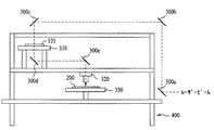
図7は本発明に係る結晶化装備を示した概略的な斜視図で、図8は本発明に係る結晶化装備のマスクステージ及び基板ステージを示した断面図で、図9は図8のマスクステージを示した平面図である。 FIG. 7 is a schematic perspective view showing the crystallization equipment according to the present invention, FIG. 8 is a sectional view showing the mask stage and the substrate stage of the crystallization equipment according to the present invention, and FIG. 9 is the mask of FIG. It is the top view which showed the stage.
図7乃至図9に示したように、本発明の結晶化装備400は、レーザービームを出射するレーザービーム発生装置(図示せず)と、複数の領域が形成されたマスク120と、前記マスク120が装着され、前記マスク120の選択的な領域に前記レーザービームが透過されるように前記マスク120を移動させるマスクステージ310と、前記マスク120の微細移動を調節するティルト手段317及びレベル手段315と、前記マスク120に対する基板200上の照射部位が変更されるように前記基板200を装着して移動させる基板ステージ330とを含んで成る。 7 to 9, the
そして、本発明の結晶化装備400には前記レーザービームの発生経路を変更するために1つ以上のミラー300(図8の300a、300b、300c、300d、300e参考)と、前記レーザービームがマスク120に透過される前に前記レーザービームを集束する集束レンズ(図示せず、従来技術参照)と、前記マスク120に透過されたレーザービームを縮小させ、前記基板200上に該当パターンで透過させるプロジェクションレンズ320が更に具備される。 The
上述した集束レンズ及びプロジェクションレンズ、ミラー300、マスク120及びマスクステージ310からなる光学手段は、前記基板ステージ330の上部に位置して基板200の流入(ローディング)時に前記基板200の該当部位にレーザービームが適切なパターンで照射されるようにして結晶化が進められるようにする。 The optical means including the focusing lens and projection lens, the
ここで、前記マスク120は複数の領域に区分されて各領域別に異形のパターンが定義されている。例えば、前記マスク120は、基板200上にアラインキー210a、201b、210c、210dを形成するためのアラインキー形成パターンが定義された第1領域と、表示部及び駆動回路部の結晶化のための第2領域とで区分されている。 Here, the
そして、前記マスクステージ310は別途のティルト手段317と、レベル手段315とを具備して、マスク120が外部から流入した時、異状位置を補正する。
即ち、前記マスク120が中心で捩じれた場合、前記ティルト手段317を回転させて位置補正を行い、前記マスク120が中心から一方に片寄った場合、また反対に横又は縦の水平面上の移動を通じて位置補正をする。The
That is, when the
そして、前記マスク120が水平に装着されなかった場合、前記マスクステージ310の角に装着されたレベル手段315のうち、一部又は全部を用いて高さを補正する。この場合にはマイクロメートル(μm)単位の細密な精密度が要求される。
前記マスク120が前記マスクステージ310上に装着された後には前記マスク120が定義された各領域別に照射部位が対応するように前記マスクステージ310を移動させてアラインキーの形成及び結晶化を進める。If the
After the
即ち、該当領域に対するレーザー照射を完了した後、次の領域に照射部位を対応させるために前記マスクステージ310を領域の大きさだけ移動させる。 That is, after completing the laser irradiation on the corresponding region, the
図10は本発明の結晶化方法に用いられるマスクを示した平面図で、図11は図10の第1領域に具備されたパターンを示した拡大図で、図12は本発明の結晶化方法によって形成されたアラインキーを示した拡大図である。
図10に示したように、本発明の結晶化方法に用いられるマスクはアラインキー形成のための第1領域と、結晶化領域を更に二分して、表示部の半導体層形成部に対する結晶化を進める第2領域と、駆動回路部に対する結晶化を進める第3領域とに分けることができる。10 is a plan view showing a mask used in the crystallization method of the present invention, FIG. 11 is an enlarged view showing a pattern provided in the first region of FIG. 10, and FIG. 12 is a crystallization method of the present invention. It is the enlarged view which showed the alignment key formed by.
As shown in FIG. 10, the mask used in the crystallization method of the present invention further divides the first region for forming the alignment key and the crystallization region into two parts, and crystallizes the semiconductor layer forming portion of the display portion. It can be divided into a second region to be advanced and a third region to promote crystallization of the driver circuit portion.

前記アラインキー形成用パターン130には複数の微少パターン135が同一の間隔で離隔して形成されている。
前記第1領域のアラインキー形成用パターン130を通じて基板の角に該当する部位を照射してアラインキーを形成する。この場合、レーザービームのエネルギー密度は、非晶質シリコン層を完全溶融する時以上のエネルギー密度、つまり照射部位の非晶質シリコン層がアブレーションされ除去することができる程度にする。In the alignment
An alignment key is formed by irradiating a portion corresponding to a corner of the substrate through the alignment
前記マスク120の第1領域を用いたレーザーの照射で形成されるアラインキー(図15の210参照)は基板200上の四つの角に形成されるので、前記第1領域のアラインキー形成用パターン130に対する透過部位が前記基板200上の各部位に対応するように基板ステージ330を上下左右に移動させ照射工程を進める。 Since the alignment keys (see 210 in FIG. 15) formed by laser irradiation using the first region of the
図7を参考にすると、このように第1領域のアラインキー形成用パターン130を用いて形成したアラインキーは、前記基板200の各エッジのうち、それぞれ右側の上部から時計方向に第1乃至第4アラインキー210a、210b、210c、210dに形成される。 Referring to FIG. 7, the alignment keys formed using the alignment
前記アラインキー210は前記マスク120の第1領域に形成されたアラインキー形成用パターン130の形象に従ったもので、その大きさは前記マスク120の第1領域に形成されたアラインキー形成用パターン130の大きさがプロジェクションレンズ320の縮小比で縮小された大きさである。 The
図13は図10の第2領域に具備された一つのパターン及びその拡大図である。
図13に示したように、前記マスク120の第2領域は表示部の半導体層形成部に対応するパターンブロック142を一つ以上具備して形成される。即ち、前記第2領域内に基板上の表示部に対応して複数の画素領域140が定義され、前記各画素領域ごとに形成される半導体層形成部に対応してパターンブロック142が形成される。FIG. 13 is one pattern provided in the second region of FIG. 10 and an enlarged view thereof.
As shown in FIG. 13, the second region of the
前記それぞれのパターンブロック142は複数の透過部143及び遮断部144が交互に繰り返して形成される。
前記パターンブロック142の大きさは前記基板200上の半導体層形成部とプロジェクションレンズ320の縮小比(5倍縮小又は4倍の比)を考慮して決定する。即ち、前記半導体層形成部の大きさに縮小比をかけた値によって前記パターンブロック142の大きさを決定する。Each pattern block 142 includes a plurality of
The size of the pattern block 142 is determined in consideration of a reduction ratio (5 times reduction or 4 times ratio) between the semiconductor layer forming portion on the
実際、基板上に形成される半導体層は薄膜トランジスタ(素子)形成部位に対応し、前記素子の大きさは横、縦約1〜100μmの大きさに該当するので、一般的な結晶化用マスクに比べてその大きさが相当に小さい。特に、結晶化用マスクは、透過部の幅を2〜10μm(実際マスクデザイン上では前記基板上の前記幅の4〜5倍(マスクを用いて基板上に照射する時、光学レンズの縮小比を考慮))の大きさにし、透過部の長さを数mm(10〜30mm、実際マスクでは前記長さの4〜5倍)にする傾向があるが、これに比べて本発明のマスクの第2領域に形成されるパターンブロック142の各透過部143の長さは相当短くなる。 Actually, the semiconductor layer formed on the substrate corresponds to a thin film transistor (element) formation site, and the size of the element corresponds to a size of about 1 to 100 μm in width and length. The size is considerably smaller than that. In particular, in the crystallization mask, the width of the transmission part is 2 to 10 μm (in actual mask design, 4 to 5 times the width on the substrate (when the mask is used to irradiate the substrate, the reduction ratio of the optical lens). )), And the length of the transmission part tends to be several mm (10 to 30 mm, 4 to 5 times the length in the actual mask). The length of each
図10に示したように、前記マスク120の第3領域には一般的な結晶化用マスクのように、透過部150及び遮断部151が繰り返されたパターンを形成する。 As shown in FIG. 10, a pattern in which the
前記透過部150の幅(L)は遮断部151の幅(S)と同じか小さくして形成する。
前記透過部150と遮断部151の幅が同じである場合(L=S)は基板上の前記マスクの第3領域パターンの対応する単位領域は2回のシャット(この場合、二回目の照射時は一回目の照射時の遮断部151に対応していた部位が透過部150に対応するように基板ステージを移動させて結晶化を進める)で結晶化が可能であり、前記透過部150の幅(L)が前記遮断部151の幅(S)より小さい場合は、それ以上の回数で照射することで単位領域の結晶化が可能となる。前者の結晶化方式をシングルスキャン、後者の結晶化方式をマルチスキャンと言う。The width (L) of the
When the widths of the
一方、透過部150の幅(L)を前記遮断部151の幅(S)より広く形成しない理由は、この場合、レーザービームの照射に対して前記マスク120が受ける熱量が非常に高くなり、前記マスク120が破損するおそれがあるからである。 On the other hand, the reason why the width (L) of the
以下、上述した結晶化装備及び複数の領域が定義されたマスクを用いた本発明の結晶化方法を順序図及び図面を通して説明する。 Hereinafter, the crystallization method of the present invention using the above-described crystallization equipment and a mask in which a plurality of regions are defined will be described with reference to a flow chart and drawings.
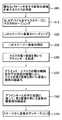
図14は本発明の結晶化方法を示した順序図である。
図14に示したように、本発明の結晶化方法は、まず、図10に示したように、異形のパターンで複数の領域が定義されたマスク120を用意する(100S)。ここでは、前記マスク120に3つの領域が定義されていると仮定する。
次いで、前記マスク120を結晶化装備内のマスクステージ310上に装着させる(101S)。FIG. 14 is a flow chart showing the crystallization method of the present invention.
As shown in FIG. 14, in the crystallization method of the present invention, first, as shown in FIG. 10, a
Next, the
次いで、基板ステージ330上に基板をローディングする(102S)。
前記基板は中央に画像を表示する表示部と、前記表示部周辺の非表示部とで区分される。そして、前記基板上にはバッファー層と非晶質シリコン層が順次に蒸着されている。Next, the substrate is loaded onto the substrate stage 330 (102S).
The substrate is divided into a display unit that displays an image in the center and a non-display unit around the display unit. A buffer layer and an amorphous silicon layer are sequentially deposited on the substrate.
次いで、前記基板ステージ330の真空ホールなどの固定手段を通じて基板を固定させる(103S)。 Next, the substrate is fixed through fixing means such as a vacuum hole of the substrate stage 330 (103S).
次いで、前記マスクの第1領域の第1パターン(アラインキー形成用パターン)を用いて前記基板上の各エッジ領域にアラインキーを形成する(104S)。
この際、前記アラインキーの形成は該当照射部位の非晶質シリコン層をアブレーションするエネルギー密度で照射して成される。Next, an alignment key is formed in each edge region on the substrate using a first pattern (alignment key formation pattern) in the first region of the mask (104S).
At this time, the alignment key is formed by irradiating the amorphous silicon layer at the irradiation site with an energy density for ablation.
次いで、前記基板上に形成されたアラインキーとの離隔程度を感知し、かつ隣接したアラインキー間の仮想の連結線上と平行するように結晶化方向を調節して、前記基板上の各画素に位置した半導体層形成部に結晶化を進める(105S)。 Next, the degree of separation from the alignment key formed on the substrate is sensed, and the crystallization direction is adjusted to be parallel to a virtual connection line between adjacent alignment keys, so that each pixel on the substrate is adjusted. Crystallization proceeds to the located semiconductor layer forming portion (105S).
次いで、前記基板上に形成された隣接したアラインキー間の仮想の連結線上と平行するように結晶化方向を調節して、前記基板上の非表示部に形成される駆動回路部に結晶化を進める(106S)。 Next, the driving circuit unit formed on the non-display portion on the substrate is crystallized by adjusting a crystallization direction so as to be parallel to a virtual connection line between adjacent alignment keys formed on the substrate. Advance (106S).
以上(105S、106S)のような前記マスクの第1、第2結晶化領域を用いたレーザービーム照射は、該当照射部位の非晶質シリコン層を完全に溶融する程度のエネルギー密度で照射する。 The laser beam irradiation using the first and second crystallized regions of the mask as described above (105S, 106S) is performed with an energy density sufficient to completely melt the amorphous silicon layer at the irradiation site.
前記マスクの第1、第2結晶化領域を用いたレーザービーム照射は、共に同一のラインに形成される素子のチャンネルにかかるグレインバウンダリーの個数と等しくなるように行われる。この時、前記同一のラインに形成される素子のチャンネルにかかるグレインバウンダリー個数の調整は、前記隣接したアラインキーの仮想の連結線と結晶化進行方向を平行にして行う。 Laser beam irradiation using the first and second crystallized regions of the mask is performed so as to be equal to the number of grain boundaries applied to the channel of the element formed on the same line. At this time, the adjustment of the number of grain boundaries applied to the channel of the element formed on the same line is performed in parallel with the imaginary connection line of the adjacent alignment key and the crystallization progress direction.
前記マスクの第1、第2結晶化領域を用いたレーザービーム照射は、前記隣接したアラインキーの仮想の連結線と結晶化進行方向を平行にさせて行われる。 Laser beam irradiation using the first and second crystallization regions of the mask is performed with the imaginary connection lines of the adjacent alignment keys parallel to the crystallization progress direction.
次いで、前記基板を基板ステージでアンローディングして外部に流出(107S)させて次の工程に対して待機させる。
アラインキー形成(104S)又は結晶化(105S、106S)のように前記マスクの一つの領域を用いたレーザービーム照射時には残りの領域はブロックされる。Next, the substrate is unloaded on the substrate stage and flows out (107S) to the outside, and the next process is waited.
The remaining regions are blocked during laser beam irradiation using one region of the mask, such as align key formation (104S) or crystallization (105S, 106S).
一方、図10のマスクは全て3つの領域に分けられて定義されているが、アラインキー領域と結晶化領域の2つの領域に定義されたマスクも利用可能である。
この場合には前記マスクの結晶化を用いて基板上の表示部の結晶化と非表示部の駆動回路部の結晶化を全て進めるという点を除いては、上述した図10のマスクを用いて結晶化する方法と同様である。On the other hand, although the masks in FIG. 10 are all defined by being divided into three regions, masks defined in two regions, an alignment key region and a crystallization region, can also be used.
In this case, the mask of FIG. 10 described above is used except that the crystallization of the display portion on the substrate and the crystallization of the driving circuit portion of the non-display portion are all advanced using the crystallization of the mask. This is the same as the crystallization method.
図15は本発明の結晶化方法を用いて結晶化時に基板に形成される各結晶化領域を示した平面図である。図15に示したように、本発明の結晶化方法を用いた結晶化時の照射部位は、大きく3つの領域に区分される。即ち、アラインキー210a、210b、210c、210dと、表示部220と、ゲートドライバー230a、230b及びソースドライバー240a、240bの駆動回路部との3つに区分することができる。 FIG. 15 is a plan view showing each crystallization region formed on the substrate during crystallization using the crystallization method of the present invention. As shown in FIG. 15, the irradiation site at the time of crystallization using the crystallization method of the present invention is roughly divided into three regions. That is, it can be divided into three parts: the
図示の図面はゲートドライバー230a、230b及びソースドライバー240a、 240bが表示部220の左右又は上下にデュアル構成されたことを示している。薄膜トランジスタアレイが形成される基板は、一般的に前記駆動回路部、つまりゲートドライバー及びソースドライバーがそれぞれ一つずつゲートラインと垂直となる一方と、データラインと垂直となる他方とに形成されるこのような構成は、駆動回路部の迅速な動作を考慮した構造である。 The illustrated drawing shows that the
結晶化順序はまず、アラインキー210a、210b、210c、210dを形成した後、表示部220と、駆動回路部230a、230b、240a、240bの順序で進める。場合によって、駆動回路部230a、230b、240a、240bに対して先に進行した後、表示部220に対する結晶化を進めることができる。 First, the
前記表示部220は、上述したように、半導体層形成部に対応して選択的に結晶化を進行することができ、以下で説明する他の結晶化方法のように、表示部220全体に対して結晶化を進行することもできる。 As described above, the
前記駆動回路部は、図面上で縦方向に形成されたゲートドライバー230a、230bと、横方向に形成されたソースドライバー240a、240bがあるが、結晶化順序はいずれのドライバーに対して先に進行しても構わない。 The driving circuit unit includes
この時、マスク120の第3領域を用いて基板200を照射して、一方のドライバーに対して結晶化を進めた後には前記マスクステージ310又は基板ステージ330を90゜回転させ、各ドライバーに形成される一ラインの素子に対して同一の方向のグレインバウンダリーが形成されるようにする。 At this time, after the
一方、マスク120の第3領域を用いた結晶化方法は、図15に示したように、非表示部から両方向にゲートドライバー及びソースドライバーが定義される基板ばかりでなく、一方向にゲートドライバー及びソースドライバーが定義される基板の場合にも利用可能である。 On the other hand, as shown in FIG. 15, the crystallization method using the third region of the
以下、本発明の異なる実施形態による結晶化方法を説明する。 Hereinafter, crystallization methods according to different embodiments of the present invention will be described.
これは表示部で半導体層形成部のみを選択的に結晶化するものではなく、表示部全体と駆動回路部に対して同一のマスクを用いて結晶化を進めるものである。 即ち、本発明の異なる実施形態による結晶化方法は、まず、図15に示したように、表示部220と、前記表示部220の周囲に非表示部(表示部以外の領域)が定義された基板200を用意する。 This does not selectively crystallize only the semiconductor layer forming portion in the display portion, but promotes crystallization using the same mask for the entire display portion and the drive circuit portion. That is, in the crystallization method according to another embodiment of the present invention, first, as shown in FIG. 15, the
次いで、前記基板200の全面にバッファー層(図示せず)を形成する。 Next, a buffer layer (not shown) is formed on the entire surface of the
次いで、前記バッファー層の全面に非晶質シリコン層(図示せず)を形成する。 Next, an amorphous silicon layer (not shown) is formed on the entire surface of the buffer layer.
次いで、前記基板200上にアラインキー領域と結晶化領域が定義されたマスク(図示せず、図10の第1領域と、第3領域のみが定義されたマスク)を対応させる。 Next, a mask in which the alignment key region and the crystallization region are defined on the substrate 200 (not shown, a mask in which only the first region and the third region in FIG. 10 are defined) is made to correspond.
次いで、前記マスクのアラインキー領域を通じて前記非表示部の所定領域にレーザービームを照射して、アラインキーを形成する。 Next, a laser beam is irradiated to a predetermined area of the non-display portion through the alignment key area of the mask to form an alignment key.
前記アラインキーは前記非表示部のそれぞれのエッジに形成される。この時、前記アラインキー形成は前記マスクのアラインキー領域を用いて該当照射部位の非晶質シリコン層をアブレーションするエネルギー密度で照射して成される。 The align key is formed at each edge of the non-display portion. At this time, the alignment key is formed by irradiating the amorphous silicon layer at the irradiation site with an energy density using the alignment key region of the mask.
次いで、前記マスクの結晶化領域を通じて前記表示部及び前記非表示部の駆動回路部にレーザービームを照射して結晶化を進行する。 Next, crystallization is performed by irradiating the driving circuit unit of the display unit and the non-display unit with a laser beam through the crystallization region of the mask.
前記マスクの結晶化領域を用いたレーザービーム照射は、該当照射部位の非晶質シリコン層を完全に溶融する程度のエネルギー密度で照射して行われる。
前記マスクの結晶化領域を用いたレーザービーム照射は、一ライン上に形成される素子のチャンネルにかかるグレインバウンダリーの個数と等しくなるように行われる。The laser beam irradiation using the crystallized region of the mask is performed by irradiating the amorphous silicon layer at the irradiation site with an energy density that completely melts the amorphous silicon layer.
The laser beam irradiation using the crystallized region of the mask is performed so as to be equal to the number of grain boundaries applied to the channel of the element formed on one line.
前記同一のラインに形成される素子のチャンネルにかかるグレインバウンダリー個数の調整は、前記隣接した一直線上のアラインキーと結晶化進行方向を平行にして調整する。
前記マスクの一領域を用いたレーザービーム照射時には前記マスクの残り領域はブロックされる。The number of grain boundaries applied to the channels of the elements formed on the same line is adjusted by making the alignment keys on the adjacent straight lines parallel to the crystallization progress direction.
At the time of laser beam irradiation using one area of the mask, the remaining area of the mask is blocked.
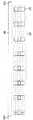
図16a及び図16bは本発明の結晶化方法によって形成された一ラインの画素に現れた素子である。
図16a及び図16bに示したように、本発明の結晶化方法は隣接したアラインキー210a、210bの仮想の連結線280と平行するように結晶化を進める。FIGS. 16A and 16B are elements appearing in a line of pixels formed by the crystallization method of the present invention.
As shown in FIGS. 16a and 16b, the crystallization method of the present invention proceeds the crystallization so as to be parallel to the
図示した図面では互いに隣接した第1、第2アラインキー210a、210bの仮想の連結線280と結晶化方向が平行である。結晶化方向に沿ってグレインバウンダリー250が形成されるが、互いに隣接した第1、第2アラインキー210a、210bの仮想の連結線280と平行に結晶化を進めるので、前記グレインバウンダリー250方向と前記結晶化方向とが一致する。 In the drawing, the crystallization direction is parallel to the
又、前記第1乃至第4アラインキー210a、210b、210c、210dを用いて結晶化以後に写真工程で半導体層(表示部の素子領域、駆動回路部)をパターニングするので、その後残された同一ライン上の素子270が前記グレインバウンダリー250方向と全て垂直して形成され、前記各素子270のチャンネルにかかったグレインバウンダリーの個数は図16aでは一つ、図16bでは二つで同一のライン線上で一致するように形成される。 In addition, since the semiconductor layer (the element region of the display portion and the drive circuit portion) is patterned by a photographic process after crystallization using the first to fourth align
このように、前記マスク120に定義された第1領域に形成されたアラインキー形成用パターン130によって結晶化前にアブレーションして形成される前記アラインキー210は、結晶化時に基板200上の照射部位と離隔程度を判断する指標になり、照射部位(結晶化部位)を制御することができ、また、隣接したアラインキーの仮想の連結線280をグレインバウンダリー250の方向で一ライン上に形成される素子のチャンネルにかかるグレインバウンダリー250の数を一致させて素子間の特性を均一にすることができる。 As described above, the
120 マスク
130 アラインキー形成用パターン
135 微少パターン
140 画素対応領域
142 パターンブロック
143 透過部
144 遮断部
150 透過部
151 遮断部
200 基板
210 アラインキー
215 オープン領域
220 表示部
230a、230b ゲートドライバー
240a、240b ソースドライバー
250 グレインバウンダリー
270 素子
280 隣接アラインキー間の仮想の連結線
300 ミラー
310 マスクステージ
315 レベル手段
317 ティルト手段
320 プロジェクションレンズ
330 基板ステージ
400 結晶化装備
120
Claims (47)
Translated fromJapaneseアラインキー領域と結晶化領域が定義されたマスクと、
前記マスクが装着され、前記マスクの選択的な領域に前記レーザービームが透過されるように前記マスクを移動させるマスクステージと、
前記マスクに対する基板上の照射部位が変更されるように前記基板を装着して移動させる基板ステージとを含んで成ることを特徴とする結晶化装備。A laser beam generator for emitting a laser beam;
A mask in which an alignment key region and a crystallization region are defined;
A mask stage which is mounted with the mask and moves the mask so that the laser beam is transmitted to a selective region of the mask;
A crystallization equipment comprising: a substrate stage for mounting and moving the substrate so that an irradiation site on the substrate with respect to the mask is changed.
前記基板の全面に非晶質シリコン層を形成する段階と、
前記基板上にアラインキー領域と結晶化領域が定義されたマスクを位置させる段階と、
前記アラインキー領域が選択されるように前記マスクを移動して、前記非表示部の所定の領域にレーザービームを照射してアラインキーを形成する段階と、
前記結晶化領域が選択されるように前記マスクを移動して、前記基板上にレーザービームを照射して前記非晶質シリコン層を結晶化する段階とを含んで成ることを特徴とする結晶化方法。Preparing a substrate having a display portion and a non-display portion defined;
Forming an amorphous silicon layer on the entire surface of the substrate;
Positioning a mask in which an alignment key region and a crystallization region are defined on the substrate;
Moving the mask so that the alignment key region is selected, and irradiating a predetermined region of the non-display portion with a laser beam to form an alignment key;
Moving the mask so that the crystallization region is selected, and irradiating a laser beam on the substrate to crystallize the amorphous silicon layer. Method.
前記基板の全面に非晶質シリコン層を形成する段階と、
前記基板の上側にアラインキー領域、第1結晶化領域、及び第2結晶化領域が定義されたマスクを位置する段階と、
前記アラインキー領域が選択されるように前記マスクを移動して、前記非表示部の所定の領域にレーザービームを照射してアラインキーを形成する段階と、
前記第1結晶化領域が選択されるように前記マスクを移動して、前記表示部の半導体層形成部にレーザービームを照射して結晶化する段階と、
前記第2結晶化領域が選択されるように前記マスクを移動して、前記非表示部の駆動回路部にレーザービームを照射して結晶化する段階とを含むことを特徴とする結晶化方法。Preparing a substrate having a display portion and a non-display portion defined;
Forming an amorphous silicon layer on the entire surface of the substrate;
Positioning a mask in which an alignment key region, a first crystallization region, and a second crystallization region are defined on the substrate;
Moving the mask so that the alignment key region is selected, and irradiating a predetermined region of the non-display portion with a laser beam to form an alignment key;
Moving the mask so that the first crystallization region is selected, and irradiating the semiconductor layer forming portion of the display portion with a laser beam to crystallize;
Moving the mask so that the second crystallization region is selected, and irradiating the drive circuit portion of the non-display portion with a laser beam for crystallization.
When the second crystallization region of the mask is used to crystallize the non-display portion of the substrate, the substrate is shifted by 90 ° to change the crystallization region from the gate driver portion to the source driver portion. The crystallization method according to claim 45.
Applications Claiming Priority (1)
| Application Number | Priority Date | Filing Date | Title |
|---|---|---|---|
| KR10-2003-0096577AKR100525443B1 (en) | 2003-12-24 | 2003-12-24 | Device for Crystallization and method for Crystallization with the same |
Publications (2)
| Publication Number | Publication Date |
|---|---|
| JP2005191560Atrue JP2005191560A (en) | 2005-07-14 |
| JP4571486B2 JP4571486B2 (en) | 2010-10-27 |
Family
ID=34698460
Family Applications (1)
| Application Number | Title | Priority Date | Filing Date |
|---|---|---|---|
| JP2004351194AExpired - Fee RelatedJP4571486B2 (en) | 2003-12-24 | 2004-12-03 | Crystallization equipment and crystallization method using the same |
Country Status (4)
| Country | Link |
|---|---|
| US (2) | US7115456B2 (en) |
| JP (1) | JP4571486B2 (en) |
| KR (1) | KR100525443B1 (en) |
| CN (1) | CN1637484B (en) |
Cited By (2)
| Publication number | Priority date | Publication date | Assignee | Title |
|---|---|---|---|---|
| JP2012522646A (en)* | 2009-04-07 | 2012-09-27 | エクシコ フランス | Method and apparatus for irradiating a semiconductor material surface with laser energy |
| WO2019031252A1 (en)* | 2017-08-10 | 2019-02-14 | 株式会社ブイ・テクノロジー | Laser irradiation device, projection mask, laser irradiation method, and program |
Families Citing this family (4)
| Publication number | Priority date | Publication date | Assignee | Title |
|---|---|---|---|---|
| JP4169071B2 (en) | 2006-05-25 | 2008-10-22 | ソニー株式会社 | Display device |
| KR101035360B1 (en)* | 2010-02-23 | 2011-05-20 | 삼성모바일디스플레이주식회사 | Laser Crystallization Apparatus and Laser Crystallization Method |
| KR101107166B1 (en) | 2010-03-12 | 2012-01-25 | 삼성모바일디스플레이주식회사 | Crystallization Method of Amorphous Silicon Film |
| KR101432156B1 (en)* | 2013-06-14 | 2014-08-20 | 에이피시스템 주식회사 | Method for processing substrate |
Citations (10)
| Publication number | Priority date | Publication date | Assignee | Title |
|---|---|---|---|---|
| JP2000035659A (en)* | 1998-07-17 | 2000-02-02 | Hitachi Denshi Ltd | Semiconductor photomask and method of forming semiconductor pattern using the photomask |
| JP2001023918A (en)* | 1999-07-08 | 2001-01-26 | Nec Corp | Semiconductor thin film forming equipment |
| JP2001142094A (en)* | 1999-11-15 | 2001-05-25 | Nec Corp | Film body part reforming device and film body part reforming method |
| JP2001148480A (en)* | 1999-11-18 | 2001-05-29 | Nec Corp | Thin film transistor and device and method for manufacturing the same |
| JP2002373845A (en)* | 2001-06-14 | 2002-12-26 | Sony Corp | Electron beam exposure method and apparatus thereof |
| JP2003022969A (en)* | 2001-05-30 | 2003-01-24 | Lg Philips Lcd Co Ltd | Silicon crystallization method using mask |
| JP2003092262A (en)* | 2001-08-21 | 2003-03-28 | Samsung Electronics Co Ltd | Polycrystalline mask and method of manufacturing polycrystalline thin film transistor using the same |
| JP2003151907A (en)* | 2001-11-08 | 2003-05-23 | Sharp Corp | 2N mask design and sequential lateral growth crystallization method |
| JP2003264198A (en)* | 2003-02-06 | 2003-09-19 | Nec Corp | Thin film transistor and electronic apparatus |
| JP2003318111A (en)* | 2002-04-17 | 2003-11-07 | Sharp Corp | Laser annealing method, shielding mask used in laser annealing method, and laser annealing apparatus |
Family Cites Families (8)
| Publication number | Priority date | Publication date | Assignee | Title |
|---|---|---|---|---|
| CA2256699C (en)* | 1996-05-28 | 2003-02-25 | The Trustees Of Columbia University In The City Of New York | Crystallization processing of semiconductor film regions on a substrate, and devices made therewith |
| JP4128271B2 (en) | 1998-06-12 | 2008-07-30 | 株式会社半導体エネルギー研究所 | Method for manufacturing semiconductor device |
| KR100324871B1 (en)* | 1999-06-25 | 2002-02-28 | 구본준, 론 위라하디락사 | Method for fabricating TFT |
| US6368945B1 (en)* | 2000-03-16 | 2002-04-09 | The Trustees Of Columbia University In The City Of New York | Method and system for providing a continuous motion sequential lateral solidification |
| KR100400510B1 (en) | 2000-12-28 | 2003-10-08 | 엘지.필립스 엘시디 주식회사 | A machine for Si crystallization and method of crystallizing Si |
| JP3831868B2 (en) | 2001-08-13 | 2006-10-11 | 大林精工株式会社 | Active matrix display device and manufacturing method thereof |
| EP1329946A3 (en)* | 2001-12-11 | 2005-04-06 | Sel Semiconductor Energy Laboratory Co., Ltd. | Manufacturing method of semiconductor device including a laser crystallization step |
| KR100496139B1 (en)* | 2002-12-30 | 2005-06-16 | 엘지.필립스 엘시디 주식회사 | optical mask, crystallization method of silicon film and manfaturing method of array substrate using the same |
- 2003
- 2003-12-24KRKR10-2003-0096577Apatent/KR100525443B1/ennot_activeExpired - Fee Related
- 2004
- 2004-09-29USUS10/951,821patent/US7115456B2/ennot_activeExpired - Lifetime
- 2004-11-25CNCN2004100917021Apatent/CN1637484B/ennot_activeExpired - Fee Related
- 2004-12-03JPJP2004351194Apatent/JP4571486B2/ennot_activeExpired - Fee Related
- 2006
- 2006-09-11USUS11/518,202patent/US7569793B2/ennot_activeExpired - Lifetime
Patent Citations (10)
| Publication number | Priority date | Publication date | Assignee | Title |
|---|---|---|---|---|
| JP2000035659A (en)* | 1998-07-17 | 2000-02-02 | Hitachi Denshi Ltd | Semiconductor photomask and method of forming semiconductor pattern using the photomask |
| JP2001023918A (en)* | 1999-07-08 | 2001-01-26 | Nec Corp | Semiconductor thin film forming equipment |
| JP2001142094A (en)* | 1999-11-15 | 2001-05-25 | Nec Corp | Film body part reforming device and film body part reforming method |
| JP2001148480A (en)* | 1999-11-18 | 2001-05-29 | Nec Corp | Thin film transistor and device and method for manufacturing the same |
| JP2003022969A (en)* | 2001-05-30 | 2003-01-24 | Lg Philips Lcd Co Ltd | Silicon crystallization method using mask |
| JP2002373845A (en)* | 2001-06-14 | 2002-12-26 | Sony Corp | Electron beam exposure method and apparatus thereof |
| JP2003092262A (en)* | 2001-08-21 | 2003-03-28 | Samsung Electronics Co Ltd | Polycrystalline mask and method of manufacturing polycrystalline thin film transistor using the same |
| JP2003151907A (en)* | 2001-11-08 | 2003-05-23 | Sharp Corp | 2N mask design and sequential lateral growth crystallization method |
| JP2003318111A (en)* | 2002-04-17 | 2003-11-07 | Sharp Corp | Laser annealing method, shielding mask used in laser annealing method, and laser annealing apparatus |
| JP2003264198A (en)* | 2003-02-06 | 2003-09-19 | Nec Corp | Thin film transistor and electronic apparatus |
Cited By (3)
| Publication number | Priority date | Publication date | Assignee | Title |
|---|---|---|---|---|
| JP2012522646A (en)* | 2009-04-07 | 2012-09-27 | エクシコ フランス | Method and apparatus for irradiating a semiconductor material surface with laser energy |
| JP2016006882A (en)* | 2009-04-07 | 2016-01-14 | レイザー システムズ アンド ソリューションズ オブ ヨーロッパLaser Systems And Solutions Of Europe | Method and apparatus for irradiating a semiconductor material surface with laser energy |
| WO2019031252A1 (en)* | 2017-08-10 | 2019-02-14 | 株式会社ブイ・テクノロジー | Laser irradiation device, projection mask, laser irradiation method, and program |
Also Published As
| Publication number | Publication date |
|---|---|
| JP4571486B2 (en) | 2010-10-27 |
| US20070063200A1 (en) | 2007-03-22 |
| KR100525443B1 (en) | 2005-11-02 |
| CN1637484A (en) | 2005-07-13 |
| US7115456B2 (en) | 2006-10-03 |
| CN1637484B (en) | 2010-04-28 |
| KR20050064962A (en) | 2005-06-29 |
| US20050142050A1 (en) | 2005-06-30 |
| US7569793B2 (en) | 2009-08-04 |
Similar Documents
| Publication | Publication Date | Title |
|---|---|---|
| KR100698056B1 (en) | Laser beam pattern mask and crystallization method using the same | |
| US7892704B2 (en) | Mask for silicon crystallization, method for crystallizing silicon using the same and display device | |
| US8207050B2 (en) | Laser mask and crystallization method using the same | |
| US8470696B2 (en) | Laser mask and crystallization method using the same | |
| US7816196B2 (en) | Laser mask and crystallization method using the same | |
| KR100531416B1 (en) | Device used in Sequential Lateral Solidification and Method for Crystallizing Silicon with the same | |
| KR101066478B1 (en) | Laser beam pattern mask and crystallization method using the same | |
| US7569793B2 (en) | Sequential lateral solidification device and method of crystallizing silicon using the same | |
| KR100720452B1 (en) | Laser irradiation apparatus and silicon crystallization method using the same | |
| KR100885013B1 (en) | Thin Film Transistors and Liquid Crystal Displays | |
| KR100546711B1 (en) | Laser irradiation apparatus and silicon crystallization method using the same | |
| KR100531413B1 (en) | Crystallization Method of Silicon | |
| KR20050066316A (en) | Device for crystallization silicon | |
| KR100652056B1 (en) | Stage, apparatus for crystallization silicon and method for crystallization silicon using the same | |
| KR20040099838A (en) | Method of Crystallizing Silicon | |
| JP2005175257A (en) | Method for producing crystalline film | |
| JP2005175380A (en) | Manufacturing method of semiconductor device, semiconductor device and indicating device, substrate used for semiconductor device and substrate used for indicating device |
Legal Events
| Date | Code | Title | Description |
|---|---|---|---|
| A131 | Notification of reasons for refusal | Free format text:JAPANESE INTERMEDIATE CODE: A131 Effective date:20080716 | |
| A601 | Written request for extension of time | Free format text:JAPANESE INTERMEDIATE CODE: A601 Effective date:20081016 | |
| A521 | Request for written amendment filed | Free format text:JAPANESE INTERMEDIATE CODE: A523 Effective date:20081017 | |
| A602 | Written permission of extension of time | Free format text:JAPANESE INTERMEDIATE CODE: A602 Effective date:20081021 | |
| A131 | Notification of reasons for refusal | Free format text:JAPANESE INTERMEDIATE CODE: A131 Effective date:20081201 | |
| A601 | Written request for extension of time | Free format text:JAPANESE INTERMEDIATE CODE: A601 Effective date:20090302 | |
| A602 | Written permission of extension of time | Free format text:JAPANESE INTERMEDIATE CODE: A602 Effective date:20090305 | |
| A601 | Written request for extension of time | Free format text:JAPANESE INTERMEDIATE CODE: A601 Effective date:20090401 | |
| A602 | Written permission of extension of time | Free format text:JAPANESE INTERMEDIATE CODE: A602 Effective date:20090406 | |
| A601 | Written request for extension of time | Free format text:JAPANESE INTERMEDIATE CODE: A601 Effective date:20090501 | |
| A602 | Written permission of extension of time | Free format text:JAPANESE INTERMEDIATE CODE: A602 Effective date:20090511 | |
| A02 | Decision of refusal | Free format text:JAPANESE INTERMEDIATE CODE: A02 Effective date:20090810 | |
| A521 | Request for written amendment filed | Free format text:JAPANESE INTERMEDIATE CODE: A523 Effective date:20091210 | |
| A911 | Transfer to examiner for re-examination before appeal (zenchi) | Free format text:JAPANESE INTERMEDIATE CODE: A911 Effective date:20100128 | |
| A131 | Notification of reasons for refusal | Free format text:JAPANESE INTERMEDIATE CODE: A131 Effective date:20100310 | |
| A521 | Request for written amendment filed | Free format text:JAPANESE INTERMEDIATE CODE: A523 Effective date:20100610 | |
| TRDD | Decision of grant or rejection written | ||
| A01 | Written decision to grant a patent or to grant a registration (utility model) | Free format text:JAPANESE INTERMEDIATE CODE: A01 Effective date:20100721 | |
| A01 | Written decision to grant a patent or to grant a registration (utility model) | Free format text:JAPANESE INTERMEDIATE CODE: A01 | |
| A61 | First payment of annual fees (during grant procedure) | Free format text:JAPANESE INTERMEDIATE CODE: A61 Effective date:20100812 | |
| FPAY | Renewal fee payment (event date is renewal date of database) | Free format text:PAYMENT UNTIL: 20130820 Year of fee payment:3 | |
| R150 | Certificate of patent or registration of utility model | Ref document number:4571486 Country of ref document:JP Free format text:JAPANESE INTERMEDIATE CODE: R150 Free format text:JAPANESE INTERMEDIATE CODE: R150 | |
| R250 | Receipt of annual fees | Free format text:JAPANESE INTERMEDIATE CODE: R250 | |
| R250 | Receipt of annual fees | Free format text:JAPANESE INTERMEDIATE CODE: R250 | |
| R250 | Receipt of annual fees | Free format text:JAPANESE INTERMEDIATE CODE: R250 | |
| R250 | Receipt of annual fees | Free format text:JAPANESE INTERMEDIATE CODE: R250 | |
| R250 | Receipt of annual fees | Free format text:JAPANESE INTERMEDIATE CODE: R250 | |
| R250 | Receipt of annual fees | Free format text:JAPANESE INTERMEDIATE CODE: R250 | |
| R250 | Receipt of annual fees | Free format text:JAPANESE INTERMEDIATE CODE: R250 | |
| LAPS | Cancellation because of no payment of annual fees |