JP2005183880A - SUBSTRATE FOR MULTILAYER WIRING BOARD, DOUBLE WIRE WIRING BOARD AND METHOD FOR PRODUCING THEM - Google Patents
SUBSTRATE FOR MULTILAYER WIRING BOARD, DOUBLE WIRE WIRING BOARD AND METHOD FOR PRODUCING THEMDownload PDFInfo
- Publication number
- JP2005183880A JP2005183880AJP2003426392AJP2003426392AJP2005183880AJP 2005183880 AJP2005183880 AJP 2005183880AJP 2003426392 AJP2003426392 AJP 2003426392AJP 2003426392 AJP2003426392 AJP 2003426392AJP 2005183880 AJP2005183880 AJP 2005183880A
- Authority
- JP
- Japan
- Prior art keywords
- bump
- insulating
- layer
- metal layer
- wiring board
- Prior art date
- Legal status (The legal status is an assumption and is not a legal conclusion. Google has not performed a legal analysis and makes no representation as to the accuracy of the status listed.)
- Granted
Links
Images


Landscapes
- Production Of Multi-Layered Print Wiring Board (AREA)
- Printing Elements For Providing Electric Connections Between Printed Circuits (AREA)
Abstract
Translated fromJapaneseDescription
Translated fromJapaneseこの発明は、多層配線板用基材、両面配線板およびそれらの製造方法に関し、特に、導電性のバンプによって層間導通を得る構造の多層配線板用基材、両面配線板およびそれらの製造方法に関するものである。 TECHNICAL FIELD The present invention relates to a multilayer wiring board substrate, a double-sided wiring board, and a method for producing them, and more particularly, to a multilayer wiring board substrate having a structure for obtaining interlayer conduction by conductive bumps, a double-sided wiring board, and a method for producing them. Is.
従来、導体回路となる金属層上にエッチング等によって金属製のバンプ(突起)を形成し、この金属層のバンプ形成面に、層間絶縁層となる接着シートをバンプ頂部が露出するように接着し、前記バンプが層間導通部をなす構造の多層配線板用基材がある(例えば、特許文献1、2参照)。 Conventionally, metal bumps (projections) are formed on a metal layer to be a conductor circuit by etching or the like, and an adhesive sheet to be an interlayer insulating layer is adhered to the bump forming surface of the metal layer so that the top of the bump is exposed. There is a multilayer wiring board substrate having a structure in which the bumps form interlayer conductive portions (see, for example,
また、この多層配線板用基材の層間絶縁層上に別の金属層を貼り合わせることにより、両面配線板が得られる。 Moreover, a double-sided wiring board is obtained by bonding another metal layer on the interlayer insulation layer of this multilayer wiring board substrate.
上述のような多層配線板用基材、両面配線板では、バンプによる層間導通が確実に行われるよう、バンプ頂部が層間絶縁層となる接着シートから確実に露出し、この露出部においてバンプが、絶縁物を挟み込むことなく層間絶縁層上の別の金属層と直接接触していなくてはならないものである。
しかしながら、接着シートを、バンプ頂部が突き出るように金属層のバンプ形成面に接着(ラミネート)しただけでは、バンプ頂部が接着シートから外部に露出しない可能性がある。このため、バンプ頂部を確実に露出させるためには、ラミネート後に、超音波カッタ等を用いて接着シート(絶縁層)表面を研削、研磨する必要が生じる。このため、以下のような問題が生じる。 However, if the adhesive sheet is simply adhered (laminated) to the bump forming surface of the metal layer so that the bump top portion protrudes, the bump top portion may not be exposed to the outside from the adhesive sheet. For this reason, in order to reliably expose the bump top, it is necessary to grind and polish the surface of the adhesive sheet (insulating layer) using an ultrasonic cutter or the like after lamination. For this reason, the following problems arise.
接着シート表面の研削、研磨は、工程数の増加を招き、さらに、接着シート表面やバンプ頂面に付着した研削研磨くず(研削研磨微粉)を除去する工程も必要で、工程数が増加する。 Grinding and polishing of the surface of the adhesive sheet invites an increase in the number of processes, and further requires a process of removing grinding and polishing debris (grinding and polishing fine powder) adhering to the surface of the adhesive sheet and the bump top surface, which increases the number of processes.
また、研削研磨くずが接着シート表面やバンプ頂面に一度付着すると、完全に排除することは難しく、バンプ頂面に研削研磨くずが付着していると、層間導通の電気的信頼性が低下する。 Also, once grinding / polishing waste adheres to the adhesive sheet surface or bump top surface, it is difficult to completely eliminate it. If grinding / polishing waste adheres to the bump top surface, the electrical reliability of interlayer conduction decreases. .
また、接着シート表面に研削研磨くずが付着していると、接着シート表面に貼り合わせる別の金属層との密着性(接着強度)が低下する。 In addition, when grinding and polishing waste adheres to the surface of the adhesive sheet, adhesion (adhesion strength) with another metal layer to be bonded to the surface of the adhesive sheet is lowered.
さらに、金属板積層時に、研削研磨くずが金属板の配線形成側に付着すると、金属板に形成する配線において導通不良を生じ易い。 Furthermore, when grinding and polishing waste adheres to the wiring forming side of the metal plate when the metal plates are laminated, conduction failure is likely to occur in the wiring formed on the metal plate.
この発明の課題は、上記従来のもののもつ問題点を排除して、絶縁接着層表面の研削、研磨を行うことなく、バンプ頂部を確実に露出させ、バンプによる層間導通について高い電気的信頼性を得ることのできる多層配線板用基材、両面配線板およびそれらの製造方法を提供することにある。 The object of the present invention is to eliminate the problems of the above-mentioned conventional ones, to reliably expose the top of the bump without grinding or polishing the surface of the insulating adhesive layer, and to provide high electrical reliability for interlayer conduction by the bump. An object of the present invention is to provide a multilayer wiring board substrate, a double-sided wiring board, and a method for producing them, which can be obtained.
この発明は上記課題を解決するものであって、請求項1に係る発明は、片面に層間導通用のバンプが形成された金属層のバンプ形成面に、接着性を有する絶縁樹脂材料をバンプ頂部を除く領域に塗布することで前記バンプの頂部が露出または突出した絶縁接着層を形成した多層配線板用基材である。 The present invention solves the above-mentioned problems, and the invention according to
請求項2に係る発明は、請求項1記載の発明において、前記絶縁接着層は、前記金属層に塗布された当該金属層の線膨張係数に近い線膨張係数を有する第1の絶縁層と、前記第1の絶縁層に塗布された接着性を有する第2の絶縁層とからなる多層配線板用基材である。 The invention according to claim 2 is the invention according to
請求項3に係る発明は、片面に層間導通用のバンプ、および、接着性を有する絶縁樹脂材料をバンプ頂部を除く領域に塗布することで前記バンプの頂部が露出または突出した絶縁接着層が形成された第1の金属層と、前記絶縁接着層で貼り合わされて前記バンプにより前記第1の金属層と層間導通された第2の金属層と、を備えている両面配線板である。 According to a third aspect of the present invention, an insulating adhesive layer in which the top of the bump is exposed or protruded is formed by applying a bump for interlayer conduction on one side and an insulating resin material having adhesiveness to a region excluding the top of the bump. A double-sided wiring board comprising: a first metal layer that is bonded, and a second metal layer that is bonded to the insulating adhesive layer and is electrically connected to the first metal layer by the bumps.
請求項4に係る発明は、請求項3記載の発明において、前記絶縁接着層は、前記第1の金属層に塗布された当該第1の金属層の線膨張係数に近い線膨張係数を有する第1の絶縁層と、前記第1の絶縁層に塗布された接着性を有する第2の絶縁層とからなる両面配線板である。 The invention according to claim 4 is the invention according to claim 3, wherein the insulating adhesive layer has a linear expansion coefficient close to a linear expansion coefficient of the first metal layer applied to the first metal layer. A double-sided wiring board comprising one insulating layer and a second insulating layer having adhesiveness applied to the first insulating layer.
請求項5に係る発明は、金属層の片面に層間導通用のバンプを形成する工程と、前記金属層のバンプ形成面に、前記バンプの配置パターンを遮蔽するマスキングを位置決めする工程と、前記マスキングを通して接着性を有する絶縁樹脂材料を塗布し、前記金属層のバンプ形成面に前記バンプの頂部が露出または突出した絶縁接着層を形成する工程と、を有する多層配線板用基材の製造方法である。 The invention according to claim 5 is the step of forming bumps for interlayer conduction on one side of the metal layer, the step of positioning masking for shielding the arrangement pattern of the bumps on the bump forming surface of the metal layer, and the masking And applying an insulating resin material having adhesiveness to form an insulating adhesive layer in which the top of the bump is exposed or protruded on the bump forming surface of the metal layer. is there.
請求項6に係る発明は、請求項5記載の発明において、前記絶縁接着層を形成する工程は、前記金属層の線膨張係数に近い線膨張係数を有する第1の絶縁樹脂材料を塗布する工程と、前記第1の絶縁樹脂材料により形成される第1の絶縁層上に、接着性を有する第2の絶縁樹脂材料を塗布する工程と、を含む多層配線板用基材の製造方法である。 The invention according to claim 6 is the invention according to claim 5, wherein the step of forming the insulating adhesive layer is a step of applying a first insulating resin material having a linear expansion coefficient close to that of the metal layer. And a step of applying a second insulating resin material having adhesiveness onto the first insulating layer formed of the first insulating resin material. .
請求項7に係る発明は、第1の金属層の片面に層間導通用のバンプを形成する工程と、前記第1の金属層のバンプ形成面に、前記バンプの配置パターンを遮蔽するマスキングを位置決めする工程と、前記マスキングを通して接着性を有する絶縁樹脂材料を塗布し、前記第1の金属層のバンプ形成面に前記バンプの頂部が露出または突出した絶縁接着層を形成する工程と、第2の金属層を前記バンプにより前記第1の金属層と層間導通を保って前記絶縁接着層で貼り合わせる工程と、を有する両面配線板の製造方法である。 According to a seventh aspect of the present invention, the step of forming a bump for interlayer conduction on one surface of the first metal layer and the masking for shielding the arrangement pattern of the bump on the bump formation surface of the first metal layer are positioned. Applying an insulating resin material having adhesiveness through the masking, forming an insulating adhesive layer in which a top portion of the bump is exposed or protruded on a bump forming surface of the first metal layer, and a second And a step of bonding the metal layer to the first metal layer by the bumps while maintaining interlayer conduction with the insulating adhesive layer.
請求項8に係る発明は、請求項7記載の発明において、前記絶縁接着層を形成する工程は、前記第1の金属層の線膨張係数に近い線膨張係数を有する第1の絶縁樹脂材料を塗布する工程と、前記第1の絶縁樹脂材料により形成される第1の絶縁層上に、接着性を有する第2の絶縁樹脂材料を塗布する工程と、を含む両面配線板の製造方法である。 The invention according to claim 8 is the invention according to claim 7, wherein in the step of forming the insulating adhesive layer, the first insulating resin material having a linear expansion coefficient close to the linear expansion coefficient of the first metal layer is used. A method for manufacturing a double-sided wiring board, comprising: a step of applying; and a step of applying a second insulating resin material having adhesiveness on a first insulating layer formed of the first insulating resin material. .
この発明は以上のように、片面に層間導通用のバンプが形成された金属層のバンプ形成面に、接着性を有する絶縁樹脂材料をバンプ頂部を除く領域に塗布することで前記バンプの頂部が露出または突出した絶縁接着層を形成するように構成したので、絶縁接着層表面の研削、研磨を行うことなく、バンプ頂部を確実に露出させ、バンプによる層間導通について高い電気的信頼性を得ることができる効果がある。 As described above, according to the present invention, the top of the bump is formed by applying an insulating resin material having adhesiveness to a region other than the top of the bump on the bump forming surface of the metal layer having the bump for interlayer conduction formed on one side. Since the insulating adhesive layer that is exposed or protruded is formed, the top of the bump is surely exposed without grinding or polishing the surface of the insulating adhesive layer, and high electrical reliability is obtained for interlayer conduction by the bump. There is an effect that can.
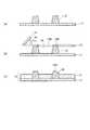
この発明による多層配線板用基材とその製造方法の一実施形態を、図1を参照して説明する。 One embodiment of a multilayer wiring board substrate and a method for producing the same according to the present invention will be described with reference to FIG.
まず、図1(a)に示すように、導体回路となる銅薄板等による金属板11上の所定位置(層間導通を行うべき各位置)に、導電性材料製のバンプ12を突出形成する。バンプ12は、銅等のエッチング、めっき、導電ペーストの印刷等により形成することができる。 First, as shown in FIG. 1 (a),
つぎに、図1(b)に示すように、金属板11のバンプ形成面上に、バンプ12の配置パターンを遮蔽するマスキング(ステンシル)13を位置決め配置する。これにより、マスキング13の遮蔽部13Aがバンプ12に対応して位置し、マスキング13の開口部13Bがバンプ12の無い部分14に対応して位置する。 Next, as shown in FIG. 1B, a masking (stencil) 13 for shielding the arrangement pattern of the
つぎに、マスキング13上から、スキージプレート15等を用いて接着性を有する絶縁材料の液状〜粘液状の樹脂前駆体16をパターン印刷する。接着性を有する絶縁材料として好適な例には熱可塑性ポリイミドがあり、熱可塑性ポリイミドの前駆体(ワニス)をスクリーン印刷法等によってパターン印刷すればよい。 Next, a liquid-
このパターン印刷により、図1(c)に示すように、バンプ12の頂部を除く部分14の金属板11上にのみ接着性を有する絶縁樹脂材料(樹脂前駆体16)が塗布され、この部分14にのみ絶縁接着層17が形成される。 By this pattern printing, as shown in FIG. 1 (c), an insulating resin material (resin precursor 16) having adhesiveness is applied only on the
これにより、バンプ12上には樹脂前駆体16が塗布されず、これに伴いバンプ12上には絶縁接着層17が全く形成されることがなく、バンプ12の頂部12Aが外部に露出した1枚の多層配線板用基材10が完成する。 As a result, the
絶縁接着層17の厚さを、バンプ12の高さ寸法より小さい厚さ寸法に設定することにより、図示されているように、バンプ12の頂部12Aが絶縁接着層17の表面より高く突出する。 By setting the thickness of the insulating
このようにして得られた多層配線板用基材10の絶縁接着層17上に、多層配線板用基材10と同等の構造で、金属板11がエッチング等によって回路形成された多層配線板用基材を積層し、加熱加圧によってプレスキュアすることにより、バンプ12を層間導通部とする多層配線板を得ることができる。 On the insulating
このとき、多層配線板用基材10のバンプ12の頂部12Aが、絶縁接着層17の表面より高く突出しているため、バンプ12による層間導通について高い電気的信頼性を得ることができる。 At this time, since the
次に、この発明による両面配線板とその製造方法の一実施形態を、図2を参照して説明する。途中までは、図1に示す多層配線板用基材10の製造方法と同様である。 Next, one embodiment of the double-sided wiring board and the manufacturing method thereof according to the present invention will be described with reference to FIG. The process is the same as that of the multilayer
まず、図2(a)に示すように、導体回路となる銅薄板等による金属板(第1の金属層)11上の所定位置(層間導通を行うべき各位置)に、導電性材料製のバンプ12を突出形成する。 First, as shown in FIG. 2 (a), a conductive material is made at a predetermined position (each position where interlayer conduction is to be performed) on a metal plate (first metal layer) 11 such as a copper thin plate to be a conductor circuit.
つぎに、図2(b)に示すように、第1の金属層11のバンプ形成面上に、バンプ12の配置パターンを遮蔽するマスキング(ステンシル)13を位置決め配置する。 Next, as shown in FIG. 2B, a masking (stencil) 13 for shielding the arrangement pattern of the
つぎに、マスキング13上から、スキージプレート15等を用いて接着性を有する絶縁材料の液状〜粘液状の樹脂前駆体16をパターン印刷する。 Next, a liquid-
このパターン印刷により、図2(c)に示すように、バンプ12の無い部分14の金属板11上にのみ接着性を有する絶縁樹脂材料(樹脂前駆体16)が塗布され、この部分14にのみ絶縁接着層17が形成される。一方、バンプ12上には樹脂前駆体16が塗布されず、バンプ12上には絶縁接着層17が全く形成されない。 By this pattern printing, as shown in FIG. 2 (c), an insulating resin material (resin precursor 16) having adhesiveness is applied only on the
絶縁接着層17の厚さを、バンプ12の高さ寸法より小さい厚さ寸法に設定することにより、図示されているように、バンプ12の頂部12Aが絶縁接着層17の表面より高く突出する。 By setting the thickness of the insulating
このようにして第1の金属層11上にバンプ12とともに形成された絶縁接着層17上に、図2(d)に示すように、導体回路となる銅薄板等による別の金属板(第2の金属層)18を積層し、加熱加圧によってプレスキュアして絶縁接着層17に金属板18を貼り合わせる。これにより、両面配線板20が得られる。 On the insulating
このとき、バンプ12の頂部12Aが、絶縁接着層17の表面より高く突出しているため、バンプ12による第1の金属層11と第2の金属層18との層間導通について、高い電気的信頼性を得ることができる。 At this time, since the
そして、金属板11、18を各々エッチングし、図2(e)に示すように、絶縁接着層17の両面に導体回路21、22を形成する。これにより、バンプ12が導体回路21と22とを互いに導通接続する層間導通部をなしている両面配線板20が得られる。 Then, the
上述したように、この実施形態による多層配線板用基材10、両面配線板20はいずれも、層間絶縁接着層となる絶縁接着層17が、バンプ12の無い部分14に対してのみの樹脂前駆体16のパターン印刷(塗布)により形成されている。これにより、絶縁接着層17に邪魔されることなく、絶縁接着層17の研削、研磨を行うことなく、研削研磨くず等の不純物の発生、残留を生じることなく、バンプ頂部12Aが絶縁接着層17から確実に外部に露出されることができる。その結果、バンプ12による層間導通について、高い電気的信頼性が安定して得られるようになる。 As described above, in both the multilayer
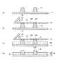
次に、この発明による多層配線板用基材とその製造方法の他の実施形態を、図3を参照して説明する。なお、図3において、図1と同様の部分には、図1に付した符号と同一の符号を付けて説明する。 Next, another embodiment of the substrate for multilayer wiring board and the method for producing the same according to the present invention will be described with reference to FIG. In FIG. 3, the same parts as those in FIG. 1 are denoted by the same reference numerals as those in FIG.
まず、図3(a)に示すように、導体回路となる銅薄板等による金属板11上の所定位置(層間導通を行うべき各位置)に、導電性材料製のバンプ12を、銅等のエッチング、めっき、あるいは導電ペーストの印刷等により突出形成する。 First, as shown in FIG. 3 (a), a
つぎに、図3(b)に示すように、金属板11のバンプ形成面上に、バンプ12の配置パターンを遮蔽するマスキング(ステンシル)13を位置決め配置する。これにより、マスキング13の遮蔽部13Aがバンプ12に対応して位置し、マスキング13の開口部13Bがバンプ12の無い部分14に対応して位置する。 Next, as shown in FIG. 3B, a masking (stencil) 13 for shielding the arrangement pattern of the
つぎに、マスキング13上から、スキージプレート15等を用いて接着性を有する絶縁材料の液状〜粘液状の樹脂前駆体31をパターン印刷する。樹脂前駆体31は、金属板11を構成する金属材料、例えば、銅の線膨張係数に近い線膨張係数を有するものを選定する。このような樹脂前駆体31としては、東レ・デュポン株式会社製のカプトン(商標)に代表されるポリイミド(全芳香族ポリイミド)やエポキシ樹脂等がある。 Next, a liquid-
このパターン印刷により、図3(c)に示すように、バンプ12の無い部分14の金属板11上にのみ樹脂前駆体31が塗布されて、絶縁接着層35の下地層(第1の絶縁層)32が形成される。下地層32の厚さは、バンプ12の高さ寸法より小さい厚さ寸法に設定される。例えば、バンプ12の高さ寸法が80μm程度であれば、下地層32の厚さは25μm程度でよい。 By this pattern printing, as shown in FIG. 3C, the
つぎに、下地層32を加熱硬化した後、図3(c)に示すように、金属板11のバンプ形成面上に、マスキング13を同様にして位置決め配置する。そして、マスキング13上から、スキージプレート15等を用いて熱可塑性ポリイミド前駆体33をパターン印刷する。 Next, after the
このパターン印刷により、図3(d)に示すように、バンプ12の無い部分14の金属板11上にのみ可塑性ポリイミド前駆体33が塗布されて、絶縁接着層35の表層(第2の絶縁層)34が形成される。表層34の厚さは、5μm程度でよく、図示されているように、バンプ12の頂部12Aが絶縁接着層35の表面より高く突出する。 By this pattern printing, as shown in FIG. 3D, the
これにより、バンプ12上には樹脂前駆体31、熱可塑性ポリイミド前駆体33の何れも塗布されず、これに伴いバンプ12上には絶縁接着層35が全く形成されることがなく、バンプ12の頂部12Aが外部に露出した1枚の多層配線板用基材30が完成する。 As a result, neither the
このようにして得られた多層配線板用基材30の絶縁接着層35上、詳細には表層34上に、多層配線板用基材30と同等の構造で、金属板11がエッチング等によって回路形成された多層配線板用基材を積層し、加熱加圧によってプレスキュアすることにより、バンプ12を層間導通部とする多層配線板を得ることができる。 On the insulating
この多層配線板用基材30の絶縁接着層35と、積層される回路形成された金属板11との接着は、熱可塑性ポリイミドによる表層34によって行われるから、良好に行われることになる。また、表層34と多層配線板用基材30の金属板11との間には、全芳香族ポリイミド等、金属板11を構成する金属材料の線膨張係数に近い線膨張係数を有する樹脂材料製の下地層32が存在するから、プレスキュア時の加熱による反りの発生が、可塑性ポリイミド単層である場合に比して小さくなる。 Adhesion between the insulating
次に、この発明による両面配線板とその製造方法の他の実施形態を、図4を参照して説明する。途中までは、図3に示す多層配線板用基材30の製造方法と同様である。 Next, another embodiment of the double-sided wiring board and the manufacturing method thereof according to the present invention will be described with reference to FIG. The process is the same as the method of manufacturing the multilayer
まず、図4(a)に示すように、導体回路となる銅薄板等による金属板(第1の金属層)11上の所定位置(層間導通を行うべき各位置)に、導電性材料製のバンプ12を突出形成する。 First, as shown in FIG. 4A, a conductive material is made at a predetermined position (each position where interlayer conduction should be performed) on a metal plate (first metal layer) 11 such as a copper thin plate to be a conductor circuit.
つぎに、図4(b)に示すように、第1の金属層11のバンプ形成面上に、バンプ12の配置パターンを遮蔽するマスキング(ステンシル)13を位置決め配置する。 Next, as shown in FIG. 4B, a masking (stencil) 13 for shielding the arrangement pattern of the
つぎに、マスキング13上から、スキージプレート15等を用いて接着性を有する絶縁材料の液状〜粘液状の樹脂前駆体31をパターン印刷する。樹脂前駆体31は、金属板11の構成材料である例えば銅の線膨張係数に近い線膨張係数を有するものを選定する。すなわち、東レ・デュポン株式会社製のカプトン(商標)に代表されるポリイミド(全芳香族ポリイミド)やエポキシ樹脂等である。 Next, a liquid-
このパターン印刷により、図4(c)に示すように、バンプ12の無い部分14の金属板11上にのみ樹脂前駆体31が塗布されて、絶縁接着層35の下地層(第1の絶縁層)32が形成される。下地層32の厚さは、バンプ12の高さ寸法より小さい厚さ寸法に設定される。例えば、バンプ12の高さ寸法が80μm程度であれば、下地層32の厚さは25μm程度でよい。 By this pattern printing, as shown in FIG. 4C, the
つぎに、下地層32を加熱硬化した後、図4(c)に示すように、金属板11のバンプ形成面上に、マスキング13を同様にして位置決め配置する。そして、マスキング13上から、スキージプレート15等を用いて熱可塑性ポリイミド前駆体33をパターン印刷する。 Next, after the
このパターン印刷により、図4(d)に示すように、バンプ12の無い部分14の金属板11上にのみ可塑性ポリイミド前駆体33が塗布されて、絶縁接着層35の表層(第2の絶縁層)34が形成される。表層34の厚さは、5μm程度でよく、図示されているように、バンプ12の頂部12Aが絶縁接着層35の表面より高く突出する。 By this pattern printing, as shown in FIG. 4D, the
これにより、バンプ12上には樹脂前駆体31、熱可塑性ポリイミド前駆体33の何れも塗布されず、これに伴いバンプ12上には絶縁接着層35が全く形成されない。 Thereby, neither the
このようにして第1の金属層11上にバンプ12とともに形成された絶縁接着層35の表層34上に、図4(e)に示すように、導体回路となる銅薄板等による別の金属板(第2の金属層)18を積層し、加熱加圧によってプレスキュアして絶縁接着層35に金属板18を貼り合わせる。これにより、両面配線板50が得られる。 On the
このとき、バンプ12の頂部12Aが、絶縁接着層35の表面より高く突出しているため、バンプ12による第1の金属層11と第2の金属層18との層間導通について、高い電気的信頼性を得ることができる。 At this time, since the
また、この絶縁接着層35と金属板18との接着は、熱可塑性ポリイミドによる表層34によって行われるから、良好に行われることになる。また、表層34と金属板11との間には、全芳香族ポリイミド等、金属板11を構成する金属材料の線膨張係数に近い線膨張係数を有する樹脂材料製の下地層32が存在するから、プレスキュア時の加熱による反りの発生が、可塑性ポリイミド単層である場合に比して小さくなる。 In addition, since the adhesion between the insulating
そして、金属板11、18を各々エッチングし、図4(f)に示すように、絶縁接着層35の両面に導体回路21、22を形成する。これにより、バンプ12が導体回路21と22とを互いに導通接続する層間導通部をなしている両面配線板50が得られる。 Then, the
上述したように、この実施形態による多層配線板用基材30、両面配線板50はいずれも、層間絶縁接着層となる絶縁接着層35(下地層32と表層34)が、バンプ12の無い部分14に対してのみの樹脂前駆体31、可塑性ポリイミド前駆体33のパターン印刷(塗布)により形成されている。これにより、絶縁接着層35に邪魔されることなく、絶縁接着層35の研削、研磨を行うことなく、研削研磨くず等の不純物の発生、残留を生じることなく、バンプ頂部12Aが絶縁接着層35から確実に外部に露出されることができる。その結果、バンプ12による層間導通について、高い電気的信頼性が安定して得られるようになる。 As described above, both of the multilayer
10 多層配線板用基材
11 金属板(第1の金属層)
12 バンプ
13 マスキング
16 樹脂前駆体
17 絶縁接着層
18 金属板(第2の金属層)
20 両面配線板
21、22 導体回路
30 多層配線板用基材
31 樹脂前駆体
32 下地層
33 可塑性ポリイミド前駆体
34 表層
35 絶縁接着層
50 両面配線板10 Multilayer Wiring
12
20 Double-
Claims (8)
Translated fromJapanese前記絶縁接着層で貼り合わされて前記バンプにより前記第1の金属層と層間導通された第2の金属層と、
を備えていることを特徴とする両面配線板。A first metal layer formed with an insulating adhesive layer in which the top of the bump is exposed or protruded by applying a bump for interlayer conduction on one side and an insulating resin material having adhesiveness to a region other than the top of the bump; ,
A second metal layer laminated with the insulating adhesive layer and interlayer-conductive with the first metal layer by the bump;
A double-sided wiring board characterized by comprising:
前記金属層のバンプ形成面に、前記バンプの配置パターンを遮蔽するマスキングを位置決めする工程と、
前記マスキングを通して接着性を有する絶縁樹脂材料を塗布し、前記金属層のバンプ形成面に前記バンプの頂部が露出または突出した絶縁接着層を形成する工程と、
を有することを特徴とする多層配線板用基材の製造方法。Forming a bump for interlayer conduction on one side of the metal layer;
Positioning a mask for shielding the bump arrangement pattern on the bump forming surface of the metal layer;
Applying an insulating resin material having adhesiveness through the masking, and forming an insulating adhesive layer in which a top portion of the bump is exposed or protruded on a bump forming surface of the metal layer; and
The manufacturing method of the base material for multilayer wiring boards characterized by having.
前記金属層の線膨張係数に近い線膨張係数を有する第1の絶縁樹脂材料を塗布する工程と、
前記第1の絶縁樹脂材料により形成される第1の絶縁層上に、接着性を有する第2の絶縁樹脂材料を塗布する工程と、
を含むことを特徴とする請求項5記載の多層配線板用基材の製造方法。The step of forming the insulating adhesive layer includes
Applying a first insulating resin material having a linear expansion coefficient close to that of the metal layer;
Applying a second insulating resin material having adhesiveness on the first insulating layer formed of the first insulating resin material;
The manufacturing method of the base material for multilayer wiring boards of Claim 5 characterized by the above-mentioned.
前記第1の金属層のバンプ形成面に、前記バンプの配置パターンを遮蔽するマスキングを位置決めする工程と、
前記マスキングを通して接着性を有する絶縁樹脂材料を塗布し、前記第1の金属層のバンプ形成面に前記バンプの頂部が露出または突出した絶縁接着層を形成する工程と、
第2の金属層を前記バンプにより前記第1の金属層と層間導通を保って前記絶縁接着層で貼り合わせる工程と、
を有することを特徴とする両面配線板の製造方法。Forming a bump for interlayer conduction on one side of the first metal layer;
Positioning a mask for shielding an arrangement pattern of the bumps on a bump forming surface of the first metal layer;
Applying an insulating resin material having adhesiveness through the masking, and forming an insulating adhesive layer in which a top of the bump is exposed or protruded on a bump forming surface of the first metal layer;
Bonding the second metal layer with the insulating adhesive layer while maintaining interlayer conduction with the first metal layer by the bump;
A method for producing a double-sided wiring board, comprising:
前記第1の金属層の線膨張係数に近い線膨張係数を有する第1の絶縁樹脂材料を塗布する工程と、
前記第1の絶縁樹脂材料により形成される第1の絶縁層上に、接着性を有する第2の絶縁樹脂材料を塗布する工程と、
を含むことを特徴とする請求項7記載の両面配線板の製造方法。The step of forming the insulating adhesive layer includes
Applying a first insulating resin material having a linear expansion coefficient close to that of the first metal layer;
Applying a second insulating resin material having adhesiveness on the first insulating layer formed of the first insulating resin material;
The manufacturing method of the double-sided wiring board of Claim 7 characterized by the above-mentioned.
Priority Applications (1)
| Application Number | Priority Date | Filing Date | Title |
|---|---|---|---|
| JP2003426392AJP4334996B2 (en) | 2003-12-24 | 2003-12-24 | SUBSTRATE FOR MULTILAYER WIRING BOARD, DOUBLE WIRE WIRING BOARD AND METHOD FOR PRODUCING THEM |
Applications Claiming Priority (1)
| Application Number | Priority Date | Filing Date | Title |
|---|---|---|---|
| JP2003426392AJP4334996B2 (en) | 2003-12-24 | 2003-12-24 | SUBSTRATE FOR MULTILAYER WIRING BOARD, DOUBLE WIRE WIRING BOARD AND METHOD FOR PRODUCING THEM |
Publications (2)
| Publication Number | Publication Date |
|---|---|
| JP2005183880Atrue JP2005183880A (en) | 2005-07-07 |
| JP4334996B2 JP4334996B2 (en) | 2009-09-30 |
Family
ID=34785947
Family Applications (1)
| Application Number | Title | Priority Date | Filing Date |
|---|---|---|---|
| JP2003426392AExpired - Fee RelatedJP4334996B2 (en) | 2003-12-24 | 2003-12-24 | SUBSTRATE FOR MULTILAYER WIRING BOARD, DOUBLE WIRE WIRING BOARD AND METHOD FOR PRODUCING THEM |
Country Status (1)
| Country | Link |
|---|---|
| JP (1) | JP4334996B2 (en) |
Cited By (49)
| Publication number | Priority date | Publication date | Assignee | Title |
|---|---|---|---|---|
| US8058101B2 (en) | 2005-12-23 | 2011-11-15 | Tessera, Inc. | Microelectronic packages and methods therefor |
| US8404520B1 (en) | 2011-10-17 | 2013-03-26 | Invensas Corporation | Package-on-package assembly with wire bond vias |
| US8482111B2 (en) | 2010-07-19 | 2013-07-09 | Tessera, Inc. | Stackable molded microelectronic packages |
| US8525314B2 (en) | 2004-11-03 | 2013-09-03 | Tessera, Inc. | Stacked packaging improvements |
| US8623706B2 (en) | 2010-11-15 | 2014-01-07 | Tessera, Inc. | Microelectronic package with terminals on dielectric mass |
| US8835228B2 (en) | 2012-05-22 | 2014-09-16 | Invensas Corporation | Substrate-less stackable package with wire-bond interconnect |
| US8878353B2 (en) | 2012-12-20 | 2014-11-04 | Invensas Corporation | Structure for microelectronic packaging with bond elements to encapsulation surface |
| US8883563B1 (en) | 2013-07-15 | 2014-11-11 | Invensas Corporation | Fabrication of microelectronic assemblies having stack terminals coupled by connectors extending through encapsulation |
| US8975738B2 (en) | 2012-11-12 | 2015-03-10 | Invensas Corporation | Structure for microelectronic packaging with terminals on dielectric mass |
| US9023691B2 (en) | 2013-07-15 | 2015-05-05 | Invensas Corporation | Microelectronic assemblies with stack terminals coupled by connectors extending through encapsulation |
| US9034696B2 (en) | 2013-07-15 | 2015-05-19 | Invensas Corporation | Microelectronic assemblies having reinforcing collars on connectors extending through encapsulation |
| US9082753B2 (en) | 2013-11-12 | 2015-07-14 | Invensas Corporation | Severing bond wire by kinking and twisting |
| US9087815B2 (en) | 2013-11-12 | 2015-07-21 | Invensas Corporation | Off substrate kinking of bond wire |
| US9093435B2 (en) | 2011-05-03 | 2015-07-28 | Tessera, Inc. | Package-on-package assembly with wire bonds to encapsulation surface |
| US9159708B2 (en) | 2010-07-19 | 2015-10-13 | Tessera, Inc. | Stackable molded microelectronic packages with area array unit connectors |
| US9214454B2 (en) | 2014-03-31 | 2015-12-15 | Invensas Corporation | Batch process fabrication of package-on-package microelectronic assemblies |
| US9224717B2 (en) | 2011-05-03 | 2015-12-29 | Tessera, Inc. | Package-on-package assembly with wire bonds to encapsulation surface |
| US9324681B2 (en) | 2010-12-13 | 2016-04-26 | Tessera, Inc. | Pin attachment |
| US9349706B2 (en) | 2012-02-24 | 2016-05-24 | Invensas Corporation | Method for package-on-package assembly with wire bonds to encapsulation surface |
| US9391008B2 (en) | 2012-07-31 | 2016-07-12 | Invensas Corporation | Reconstituted wafer-level package DRAM |
| US9412714B2 (en) | 2014-05-30 | 2016-08-09 | Invensas Corporation | Wire bond support structure and microelectronic package including wire bonds therefrom |
| US9502390B2 (en) | 2012-08-03 | 2016-11-22 | Invensas Corporation | BVA interposer |
| US9583411B2 (en) | 2014-01-17 | 2017-02-28 | Invensas Corporation | Fine pitch BVA using reconstituted wafer with area array accessible for testing |
| US9601454B2 (en) | 2013-02-01 | 2017-03-21 | Invensas Corporation | Method of forming a component having wire bonds and a stiffening layer |
| US9646917B2 (en) | 2014-05-29 | 2017-05-09 | Invensas Corporation | Low CTE component with wire bond interconnects |
| US9659848B1 (en) | 2015-11-18 | 2017-05-23 | Invensas Corporation | Stiffened wires for offset BVA |
| US9685365B2 (en) | 2013-08-08 | 2017-06-20 | Invensas Corporation | Method of forming a wire bond having a free end |
| US9691679B2 (en) | 2012-02-24 | 2017-06-27 | Invensas Corporation | Method for package-on-package assembly with wire bonds to encapsulation surface |
| US9728527B2 (en) | 2013-11-22 | 2017-08-08 | Invensas Corporation | Multiple bond via arrays of different wire heights on a same substrate |
| US9735084B2 (en) | 2014-12-11 | 2017-08-15 | Invensas Corporation | Bond via array for thermal conductivity |
| US9761554B2 (en) | 2015-05-07 | 2017-09-12 | Invensas Corporation | Ball bonding metal wire bond wires to metal pads |
| US9812402B2 (en) | 2015-10-12 | 2017-11-07 | Invensas Corporation | Wire bond wires for interference shielding |
| US9842745B2 (en) | 2012-02-17 | 2017-12-12 | Invensas Corporation | Heat spreading substrate with embedded interconnects |
| US9852969B2 (en) | 2013-11-22 | 2017-12-26 | Invensas Corporation | Die stacks with one or more bond via arrays of wire bond wires and with one or more arrays of bump interconnects |
| US9888579B2 (en) | 2015-03-05 | 2018-02-06 | Invensas Corporation | Pressing of wire bond wire tips to provide bent-over tips |
| US9911718B2 (en) | 2015-11-17 | 2018-03-06 | Invensas Corporation | ‘RDL-First’ packaged microelectronic device for a package-on-package device |
| US9935075B2 (en) | 2016-07-29 | 2018-04-03 | Invensas Corporation | Wire bonding method and apparatus for electromagnetic interference shielding |
| US9984992B2 (en) | 2015-12-30 | 2018-05-29 | Invensas Corporation | Embedded wire bond wires for vertical integration with separate surface mount and wire bond mounting surfaces |
| US10008469B2 (en) | 2015-04-30 | 2018-06-26 | Invensas Corporation | Wafer-level packaging using wire bond wires in place of a redistribution layer |
| US10008477B2 (en) | 2013-09-16 | 2018-06-26 | Invensas Corporation | Microelectronic element with bond elements to encapsulation surface |
| US10026717B2 (en) | 2013-11-22 | 2018-07-17 | Invensas Corporation | Multiple bond via arrays of different wire heights on a same substrate |
| US10181457B2 (en) | 2015-10-26 | 2019-01-15 | Invensas Corporation | Microelectronic package for wafer-level chip scale packaging with fan-out |
| US10299368B2 (en) | 2016-12-21 | 2019-05-21 | Invensas Corporation | Surface integrated waveguides and circuit structures therefor |
| US10332854B2 (en) | 2015-10-23 | 2019-06-25 | Invensas Corporation | Anchoring structure of fine pitch bva |
| CN109936919A (en)* | 2019-03-05 | 2019-06-25 | 惠州市特创电子科技有限公司 | A kind of high-frequency transmission line plate and preparation method thereof be connected by conductive paste |
| US10381326B2 (en) | 2014-05-28 | 2019-08-13 | Invensas Corporation | Structure and method for integrated circuits packaging with increased density |
| US10460958B2 (en) | 2013-08-07 | 2019-10-29 | Invensas Corporation | Method of manufacturing embedded packaging with preformed vias |
| US10490528B2 (en) | 2015-10-12 | 2019-11-26 | Invensas Corporation | Embedded wire bond wires |
| KR20230047157A (en) | 2020-09-24 | 2023-04-06 | 후지필름 가부시키가이샤 | Method for manufacturing a composite pattern, resin composition, method for manufacturing a laminate, and method for manufacturing a semiconductor device |
- 2003
- 2003-12-24JPJP2003426392Apatent/JP4334996B2/ennot_activeExpired - Fee Related
Cited By (105)
| Publication number | Priority date | Publication date | Assignee | Title |
|---|---|---|---|---|
| US8927337B2 (en) | 2004-11-03 | 2015-01-06 | Tessera, Inc. | Stacked packaging improvements |
| US9570416B2 (en) | 2004-11-03 | 2017-02-14 | Tessera, Inc. | Stacked packaging improvements |
| US9153562B2 (en) | 2004-11-03 | 2015-10-06 | Tessera, Inc. | Stacked packaging improvements |
| US8531020B2 (en) | 2004-11-03 | 2013-09-10 | Tessera, Inc. | Stacked packaging improvements |
| US8525314B2 (en) | 2004-11-03 | 2013-09-03 | Tessera, Inc. | Stacked packaging improvements |
| US9984901B2 (en) | 2005-12-23 | 2018-05-29 | Tessera, Inc. | Method for making a microelectronic assembly having conductive elements |
| US8093697B2 (en) | 2005-12-23 | 2012-01-10 | Tessera, Inc. | Microelectronic packages and methods therefor |
| US8058101B2 (en) | 2005-12-23 | 2011-11-15 | Tessera, Inc. | Microelectronic packages and methods therefor |
| US8728865B2 (en) | 2005-12-23 | 2014-05-20 | Tessera, Inc. | Microelectronic packages and methods therefor |
| US9218988B2 (en) | 2005-12-23 | 2015-12-22 | Tessera, Inc. | Microelectronic packages and methods therefor |
| US8482111B2 (en) | 2010-07-19 | 2013-07-09 | Tessera, Inc. | Stackable molded microelectronic packages |
| US10128216B2 (en) | 2010-07-19 | 2018-11-13 | Tessera, Inc. | Stackable molded microelectronic packages |
| US9159708B2 (en) | 2010-07-19 | 2015-10-13 | Tessera, Inc. | Stackable molded microelectronic packages with area array unit connectors |
| US9553076B2 (en) | 2010-07-19 | 2017-01-24 | Tessera, Inc. | Stackable molded microelectronic packages with area array unit connectors |
| US9570382B2 (en) | 2010-07-19 | 2017-02-14 | Tessera, Inc. | Stackable molded microelectronic packages |
| US8907466B2 (en) | 2010-07-19 | 2014-12-09 | Tessera, Inc. | Stackable molded microelectronic packages |
| US9123664B2 (en) | 2010-07-19 | 2015-09-01 | Tessera, Inc. | Stackable molded microelectronic packages |
| US8623706B2 (en) | 2010-11-15 | 2014-01-07 | Tessera, Inc. | Microelectronic package with terminals on dielectric mass |
| US8957527B2 (en) | 2010-11-15 | 2015-02-17 | Tessera, Inc. | Microelectronic package with terminals on dielectric mass |
| US8659164B2 (en) | 2010-11-15 | 2014-02-25 | Tessera, Inc. | Microelectronic package with terminals on dielectric mass |
| US8637991B2 (en) | 2010-11-15 | 2014-01-28 | Tessera, Inc. | Microelectronic package with terminals on dielectric mass |
| US9324681B2 (en) | 2010-12-13 | 2016-04-26 | Tessera, Inc. | Pin attachment |
| US9224717B2 (en) | 2011-05-03 | 2015-12-29 | Tessera, Inc. | Package-on-package assembly with wire bonds to encapsulation surface |
| US10593643B2 (en) | 2011-05-03 | 2020-03-17 | Tessera, Inc. | Package-on-package assembly with wire bonds to encapsulation surface |
| US11424211B2 (en) | 2011-05-03 | 2022-08-23 | Tessera Llc | Package-on-package assembly with wire bonds to encapsulation surface |
| US9093435B2 (en) | 2011-05-03 | 2015-07-28 | Tessera, Inc. | Package-on-package assembly with wire bonds to encapsulation surface |
| US9691731B2 (en) | 2011-05-03 | 2017-06-27 | Tessera, Inc. | Package-on-package assembly with wire bonds to encapsulation surface |
| US10062661B2 (en) | 2011-05-03 | 2018-08-28 | Tessera, Inc. | Package-on-package assembly with wire bonds to encapsulation surface |
| US11735563B2 (en) | 2011-10-17 | 2023-08-22 | Invensas Llc | Package-on-package assembly with wire bond vias |
| US11189595B2 (en) | 2011-10-17 | 2021-11-30 | Invensas Corporation | Package-on-package assembly with wire bond vias |
| US9761558B2 (en) | 2011-10-17 | 2017-09-12 | Invensas Corporation | Package-on-package assembly with wire bond vias |
| US9041227B2 (en) | 2011-10-17 | 2015-05-26 | Invensas Corporation | Package-on-package assembly with wire bond vias |
| US9252122B2 (en) | 2011-10-17 | 2016-02-02 | Invensas Corporation | Package-on-package assembly with wire bond vias |
| US8404520B1 (en) | 2011-10-17 | 2013-03-26 | Invensas Corporation | Package-on-package assembly with wire bond vias |
| US9105483B2 (en) | 2011-10-17 | 2015-08-11 | Invensas Corporation | Package-on-package assembly with wire bond vias |
| US8836136B2 (en) | 2011-10-17 | 2014-09-16 | Invensas Corporation | Package-on-package assembly with wire bond vias |
| US10756049B2 (en) | 2011-10-17 | 2020-08-25 | Invensas Corporation | Package-on-package assembly with wire bond vias |
| US9842745B2 (en) | 2012-02-17 | 2017-12-12 | Invensas Corporation | Heat spreading substrate with embedded interconnects |
| US9349706B2 (en) | 2012-02-24 | 2016-05-24 | Invensas Corporation | Method for package-on-package assembly with wire bonds to encapsulation surface |
| US9691679B2 (en) | 2012-02-24 | 2017-06-27 | Invensas Corporation | Method for package-on-package assembly with wire bonds to encapsulation surface |
| US9953914B2 (en) | 2012-05-22 | 2018-04-24 | Invensas Corporation | Substrate-less stackable package with wire-bond interconnect |
| US8835228B2 (en) | 2012-05-22 | 2014-09-16 | Invensas Corporation | Substrate-less stackable package with wire-bond interconnect |
| US10170412B2 (en) | 2012-05-22 | 2019-01-01 | Invensas Corporation | Substrate-less stackable package with wire-bond interconnect |
| US10510659B2 (en) | 2012-05-22 | 2019-12-17 | Invensas Corporation | Substrate-less stackable package with wire-bond interconnect |
| US9391008B2 (en) | 2012-07-31 | 2016-07-12 | Invensas Corporation | Reconstituted wafer-level package DRAM |
| US9917073B2 (en) | 2012-07-31 | 2018-03-13 | Invensas Corporation | Reconstituted wafer-level package dram with conductive interconnects formed in encapsulant at periphery of the package |
| US9502390B2 (en) | 2012-08-03 | 2016-11-22 | Invensas Corporation | BVA interposer |
| US10297582B2 (en) | 2012-08-03 | 2019-05-21 | Invensas Corporation | BVA interposer |
| US8975738B2 (en) | 2012-11-12 | 2015-03-10 | Invensas Corporation | Structure for microelectronic packaging with terminals on dielectric mass |
| US8878353B2 (en) | 2012-12-20 | 2014-11-04 | Invensas Corporation | Structure for microelectronic packaging with bond elements to encapsulation surface |
| US9615456B2 (en) | 2012-12-20 | 2017-04-04 | Invensas Corporation | Microelectronic assembly for microelectronic packaging with bond elements to encapsulation surface |
| US9095074B2 (en) | 2012-12-20 | 2015-07-28 | Invensas Corporation | Structure for microelectronic packaging with bond elements to encapsulation surface |
| US9601454B2 (en) | 2013-02-01 | 2017-03-21 | Invensas Corporation | Method of forming a component having wire bonds and a stiffening layer |
| US9633979B2 (en) | 2013-07-15 | 2017-04-25 | Invensas Corporation | Microelectronic assemblies having stack terminals coupled by connectors extending through encapsulation |
| US8883563B1 (en) | 2013-07-15 | 2014-11-11 | Invensas Corporation | Fabrication of microelectronic assemblies having stack terminals coupled by connectors extending through encapsulation |
| US9023691B2 (en) | 2013-07-15 | 2015-05-05 | Invensas Corporation | Microelectronic assemblies with stack terminals coupled by connectors extending through encapsulation |
| US9034696B2 (en) | 2013-07-15 | 2015-05-19 | Invensas Corporation | Microelectronic assemblies having reinforcing collars on connectors extending through encapsulation |
| US10460958B2 (en) | 2013-08-07 | 2019-10-29 | Invensas Corporation | Method of manufacturing embedded packaging with preformed vias |
| US9685365B2 (en) | 2013-08-08 | 2017-06-20 | Invensas Corporation | Method of forming a wire bond having a free end |
| US10008477B2 (en) | 2013-09-16 | 2018-06-26 | Invensas Corporation | Microelectronic element with bond elements to encapsulation surface |
| US9082753B2 (en) | 2013-11-12 | 2015-07-14 | Invensas Corporation | Severing bond wire by kinking and twisting |
| US9893033B2 (en) | 2013-11-12 | 2018-02-13 | Invensas Corporation | Off substrate kinking of bond wire |
| US9087815B2 (en) | 2013-11-12 | 2015-07-21 | Invensas Corporation | Off substrate kinking of bond wire |
| US10290613B2 (en) | 2013-11-22 | 2019-05-14 | Invensas Corporation | Multiple bond via arrays of different wire heights on a same substrate |
| US9852969B2 (en) | 2013-11-22 | 2017-12-26 | Invensas Corporation | Die stacks with one or more bond via arrays of wire bond wires and with one or more arrays of bump interconnects |
| US9728527B2 (en) | 2013-11-22 | 2017-08-08 | Invensas Corporation | Multiple bond via arrays of different wire heights on a same substrate |
| US10026717B2 (en) | 2013-11-22 | 2018-07-17 | Invensas Corporation | Multiple bond via arrays of different wire heights on a same substrate |
| US10629567B2 (en) | 2013-11-22 | 2020-04-21 | Invensas Corporation | Multiple plated via arrays of different wire heights on same substrate |
| USRE49987E1 (en) | 2013-11-22 | 2024-05-28 | Invensas Llc | Multiple plated via arrays of different wire heights on a same substrate |
| US10529636B2 (en) | 2014-01-17 | 2020-01-07 | Invensas Corporation | Fine pitch BVA using reconstituted wafer with area array accessible for testing |
| US11404338B2 (en) | 2014-01-17 | 2022-08-02 | Invensas Corporation | Fine pitch bva using reconstituted wafer with area array accessible for testing |
| US9583411B2 (en) | 2014-01-17 | 2017-02-28 | Invensas Corporation | Fine pitch BVA using reconstituted wafer with area array accessible for testing |
| US9837330B2 (en) | 2014-01-17 | 2017-12-05 | Invensas Corporation | Fine pitch BVA using reconstituted wafer with area array accessible for testing |
| US11990382B2 (en) | 2014-01-17 | 2024-05-21 | Adeia Semiconductor Technologies Llc | Fine pitch BVA using reconstituted wafer with area array accessible for testing |
| US9356006B2 (en) | 2014-03-31 | 2016-05-31 | Invensas Corporation | Batch process fabrication of package-on-package microelectronic assemblies |
| US9214454B2 (en) | 2014-03-31 | 2015-12-15 | Invensas Corporation | Batch process fabrication of package-on-package microelectronic assemblies |
| US9812433B2 (en) | 2014-03-31 | 2017-11-07 | Invensas Corporation | Batch process fabrication of package-on-package microelectronic assemblies |
| US10381326B2 (en) | 2014-05-28 | 2019-08-13 | Invensas Corporation | Structure and method for integrated circuits packaging with increased density |
| US10032647B2 (en) | 2014-05-29 | 2018-07-24 | Invensas Corporation | Low CTE component with wire bond interconnects |
| US9646917B2 (en) | 2014-05-29 | 2017-05-09 | Invensas Corporation | Low CTE component with wire bond interconnects |
| US10475726B2 (en) | 2014-05-29 | 2019-11-12 | Invensas Corporation | Low CTE component with wire bond interconnects |
| US9412714B2 (en) | 2014-05-30 | 2016-08-09 | Invensas Corporation | Wire bond support structure and microelectronic package including wire bonds therefrom |
| US9947641B2 (en) | 2014-05-30 | 2018-04-17 | Invensas Corporation | Wire bond support structure and microelectronic package including wire bonds therefrom |
| US9735084B2 (en) | 2014-12-11 | 2017-08-15 | Invensas Corporation | Bond via array for thermal conductivity |
| US10806036B2 (en) | 2015-03-05 | 2020-10-13 | Invensas Corporation | Pressing of wire bond wire tips to provide bent-over tips |
| US9888579B2 (en) | 2015-03-05 | 2018-02-06 | Invensas Corporation | Pressing of wire bond wire tips to provide bent-over tips |
| US10008469B2 (en) | 2015-04-30 | 2018-06-26 | Invensas Corporation | Wafer-level packaging using wire bond wires in place of a redistribution layer |
| US9761554B2 (en) | 2015-05-07 | 2017-09-12 | Invensas Corporation | Ball bonding metal wire bond wires to metal pads |
| US10490528B2 (en) | 2015-10-12 | 2019-11-26 | Invensas Corporation | Embedded wire bond wires |
| US9812402B2 (en) | 2015-10-12 | 2017-11-07 | Invensas Corporation | Wire bond wires for interference shielding |
| US10559537B2 (en) | 2015-10-12 | 2020-02-11 | Invensas Corporation | Wire bond wires for interference shielding |
| US11462483B2 (en) | 2015-10-12 | 2022-10-04 | Invensas Llc | Wire bond wires for interference shielding |
| US10115678B2 (en) | 2015-10-12 | 2018-10-30 | Invensas Corporation | Wire bond wires for interference shielding |
| US10332854B2 (en) | 2015-10-23 | 2019-06-25 | Invensas Corporation | Anchoring structure of fine pitch bva |
| US10181457B2 (en) | 2015-10-26 | 2019-01-15 | Invensas Corporation | Microelectronic package for wafer-level chip scale packaging with fan-out |
| US10043779B2 (en) | 2015-11-17 | 2018-08-07 | Invensas Corporation | Packaged microelectronic device for a package-on-package device |
| US9911718B2 (en) | 2015-11-17 | 2018-03-06 | Invensas Corporation | ‘RDL-First’ packaged microelectronic device for a package-on-package device |
| US9659848B1 (en) | 2015-11-18 | 2017-05-23 | Invensas Corporation | Stiffened wires for offset BVA |
| US10325877B2 (en) | 2015-12-30 | 2019-06-18 | Invensas Corporation | Embedded wire bond wires for vertical integration with separate surface mount and wire bond mounting surfaces |
| US9984992B2 (en) | 2015-12-30 | 2018-05-29 | Invensas Corporation | Embedded wire bond wires for vertical integration with separate surface mount and wire bond mounting surfaces |
| US10658302B2 (en) | 2016-07-29 | 2020-05-19 | Invensas Corporation | Wire bonding method and apparatus for electromagnetic interference shielding |
| US9935075B2 (en) | 2016-07-29 | 2018-04-03 | Invensas Corporation | Wire bonding method and apparatus for electromagnetic interference shielding |
| US10299368B2 (en) | 2016-12-21 | 2019-05-21 | Invensas Corporation | Surface integrated waveguides and circuit structures therefor |
| CN109936919A (en)* | 2019-03-05 | 2019-06-25 | 惠州市特创电子科技有限公司 | A kind of high-frequency transmission line plate and preparation method thereof be connected by conductive paste |
| KR20230047157A (en) | 2020-09-24 | 2023-04-06 | 후지필름 가부시키가이샤 | Method for manufacturing a composite pattern, resin composition, method for manufacturing a laminate, and method for manufacturing a semiconductor device |
Also Published As
| Publication number | Publication date |
|---|---|
| JP4334996B2 (en) | 2009-09-30 |
Similar Documents
| Publication | Publication Date | Title |
|---|---|---|
| JP4334996B2 (en) | SUBSTRATE FOR MULTILAYER WIRING BOARD, DOUBLE WIRE WIRING BOARD AND METHOD FOR PRODUCING THEM | |
| TWI386140B (en) | Flexible multilayer circuit board | |
| US7229293B2 (en) | Connecting structure of circuit board and method for manufacturing the same | |
| JP2002064271A (en) | Composite wiring board and method of manufacturing the same | |
| JP2003347748A (en) | Multilayer wiring board and its manufacturing method | |
| WO2007013595A1 (en) | Bending-type rigid printed wiring board and process for producing the same | |
| US6651324B1 (en) | Process for manufacture of printed circuit boards with thick copper power circuitry and thin copper signal circuitry on the same layer | |
| JP2007110010A (en) | Flexible printed wiring board, flexible printed circuit board, and their manufacturing method | |
| JP2008300819A (en) | Printed circuit board and method for manufacturing the same | |
| JP2009049444A (en) | Multilayer circuit board manufacturing method | |
| JP2002151853A (en) | Multilayer wiring board and manufacturing method thereof | |
| KR101204083B1 (en) | Active IC chip embedded multilayer flexible printed circuit board and Method of making the same | |
| JP2005243899A (en) | Printed wiring board and manufacturing method thereof | |
| JP2004104045A (en) | Multilayer circuit wiring board | |
| KR100699237B1 (en) | Embedded printed circuit board manufacturing method | |
| JP2007158069A (en) | External connection structure for semiconductor package and manufacturing method thereof | |
| JP2889516B2 (en) | Method for manufacturing multilayer wiring board | |
| JP2006100703A (en) | Rigid-flexible substrate and manufacturing method thereof | |
| JP3509315B2 (en) | Circuit board manufacturing method | |
| JP2000133943A (en) | Method for manufacturing multilayer substrate | |
| US20230063719A1 (en) | Method for manufacturing wiring substrate | |
| CN114828447B (en) | Circuit board and manufacturing method thereof | |
| JP2005183490A (en) | SUBSTRATE FOR MULTILAYER WIRING BOARD, DOUBLE WIRE WIRING BOARD AND METHOD FOR PRODUCING THEM | |
| JP2010087222A (en) | Method of manufacturing printed wiring board, and the printed wiring board | |
| WO2019198241A1 (en) | Method for manufacturing board with embedded components, and board with embedded components |
Legal Events
| Date | Code | Title | Description |
|---|---|---|---|
| A621 | Written request for application examination | Effective date:20060614 Free format text:JAPANESE INTERMEDIATE CODE: A621 | |
| A711 | Notification of change in applicant | Effective date:20070206 Free format text:JAPANESE INTERMEDIATE CODE: A711 | |
| A131 | Notification of reasons for refusal | Effective date:20080701 Free format text:JAPANESE INTERMEDIATE CODE: A131 | |
| A521 | Written amendment | Effective date:20080926 Free format text:JAPANESE INTERMEDIATE CODE: A523 | |
| A521 | Written amendment | Free format text:JAPANESE INTERMEDIATE CODE: A523 Effective date:20081031 | |
| RD02 | Notification of acceptance of power of attorney | Free format text:JAPANESE INTERMEDIATE CODE: A7422 Effective date:20081031 | |
| A521 | Written amendment | Free format text:JAPANESE INTERMEDIATE CODE: A821 Effective date:20081031 | |
| A131 | Notification of reasons for refusal | Effective date:20090106 Free format text:JAPANESE INTERMEDIATE CODE: A131 | |
| A521 | Written amendment | Free format text:JAPANESE INTERMEDIATE CODE: A523 Effective date:20090225 | |
| TRDD | Decision of grant or rejection written | ||
| A01 | Written decision to grant a patent or to grant a registration (utility model) | Free format text:JAPANESE INTERMEDIATE CODE: A01 Effective date:20090526 | |
| A01 | Written decision to grant a patent or to grant a registration (utility model) | Free format text:JAPANESE INTERMEDIATE CODE: A01 | |
| A61 | First payment of annual fees (during grant procedure) | Effective date:20090624 Free format text:JAPANESE INTERMEDIATE CODE: A61 | |
| FPAY | Renewal fee payment (prs date is renewal date of database) | Free format text:PAYMENT UNTIL: 20120703 Year of fee payment:3 | |
| R150 | Certificate of patent (=grant) or registration of utility model | Free format text:JAPANESE INTERMEDIATE CODE: R150 | |
| LAPS | Cancellation because of no payment of annual fees |