JP2005183770A - High frequency semiconductor devices - Google Patents
High frequency semiconductor devicesDownload PDFInfo
- Publication number
- JP2005183770A JP2005183770AJP2003424335AJP2003424335AJP2005183770AJP 2005183770 AJP2005183770 AJP 2005183770AJP 2003424335 AJP2003424335 AJP 2003424335AJP 2003424335 AJP2003424335 AJP 2003424335AJP 2005183770 AJP2005183770 AJP 2005183770A
- Authority
- JP
- Japan
- Prior art keywords
- semiconductor element
- cell
- electrode
- element group
- connection wiring
- Prior art date
- Legal status (The legal status is an assumption and is not a legal conclusion. Google has not performed a legal analysis and makes no representation as to the accuracy of the status listed.)
- Pending
Links
Images


Classifications
- H—ELECTRICITY
- H01—ELECTRIC ELEMENTS
- H01L—SEMICONDUCTOR DEVICES NOT COVERED BY CLASS H10
- H01L23/00—Details of semiconductor or other solid state devices
- H01L23/48—Arrangements for conducting electric current to or from the solid state body in operation, e.g. leads, terminal arrangements ; Selection of materials therefor
- H01L23/482—Arrangements for conducting electric current to or from the solid state body in operation, e.g. leads, terminal arrangements ; Selection of materials therefor consisting of lead-in layers inseparably applied to the semiconductor body (electrodes)
- H01L23/4821—Bridge structure with air gap
- H—ELECTRICITY
- H01—ELECTRIC ELEMENTS
- H01L—SEMICONDUCTOR DEVICES NOT COVERED BY CLASS H10
- H01L23/00—Details of semiconductor or other solid state devices
- H01L23/48—Arrangements for conducting electric current to or from the solid state body in operation, e.g. leads, terminal arrangements ; Selection of materials therefor
- H01L23/482—Arrangements for conducting electric current to or from the solid state body in operation, e.g. leads, terminal arrangements ; Selection of materials therefor consisting of lead-in layers inseparably applied to the semiconductor body (electrodes)
- H01L23/4824—Pads with extended contours, e.g. grid structure, branch structure, finger structure
- H—ELECTRICITY
- H10—SEMICONDUCTOR DEVICES; ELECTRIC SOLID-STATE DEVICES NOT OTHERWISE PROVIDED FOR
- H10D—INORGANIC ELECTRIC SEMICONDUCTOR DEVICES
- H10D30/00—Field-effect transistors [FET]
- H10D30/80—FETs having rectifying junction gate electrodes
- H10D30/87—FETs having Schottky gate electrodes, e.g. metal-semiconductor FETs [MESFET]
- H—ELECTRICITY
- H10—SEMICONDUCTOR DEVICES; ELECTRIC SOLID-STATE DEVICES NOT OTHERWISE PROVIDED FOR
- H10D—INORGANIC ELECTRIC SEMICONDUCTOR DEVICES
- H10D62/00—Semiconductor bodies, or regions thereof, of devices having potential barriers
- H10D62/10—Shapes, relative sizes or dispositions of the regions of the semiconductor bodies; Shapes of the semiconductor bodies
- H10D62/124—Shapes, relative sizes or dispositions of the regions of semiconductor bodies or of junctions between the regions
- H10D62/126—Top-view geometrical layouts of the regions or the junctions
- H—ELECTRICITY
- H10—SEMICONDUCTOR DEVICES; ELECTRIC SOLID-STATE DEVICES NOT OTHERWISE PROVIDED FOR
- H10D—INORGANIC ELECTRIC SEMICONDUCTOR DEVICES
- H10D84/00—Integrated devices formed in or on semiconductor substrates that comprise only semiconducting layers, e.g. on Si wafers or on GaAs-on-Si wafers
- H10D84/01—Manufacture or treatment
- H10D84/0123—Integrating together multiple components covered by H10D12/00 or H10D30/00, e.g. integrating multiple IGBTs
- H10D84/0126—Integrating together multiple components covered by H10D12/00 or H10D30/00, e.g. integrating multiple IGBTs the components including insulated gates, e.g. IGFETs
- H10D84/0149—Manufacturing their interconnections or electrodes, e.g. source or drain electrodes
- H—ELECTRICITY
- H10—SEMICONDUCTOR DEVICES; ELECTRIC SOLID-STATE DEVICES NOT OTHERWISE PROVIDED FOR
- H10D—INORGANIC ELECTRIC SEMICONDUCTOR DEVICES
- H10D84/00—Integrated devices formed in or on semiconductor substrates that comprise only semiconducting layers, e.g. on Si wafers or on GaAs-on-Si wafers
- H10D84/01—Manufacture or treatment
- H10D84/02—Manufacture or treatment characterised by using material-based technologies
- H10D84/03—Manufacture or treatment characterised by using material-based technologies using Group IV technology, e.g. silicon technology or silicon-carbide [SiC] technology
- H10D84/038—Manufacture or treatment characterised by using material-based technologies using Group IV technology, e.g. silicon technology or silicon-carbide [SiC] technology using silicon technology, e.g. SiGe
- H—ELECTRICITY
- H01—ELECTRIC ELEMENTS
- H01L—SEMICONDUCTOR DEVICES NOT COVERED BY CLASS H10
- H01L2924/00—Indexing scheme for arrangements or methods for connecting or disconnecting semiconductor or solid-state bodies as covered by H01L24/00
- H01L2924/0001—Technical content checked by a classifier
- H01L2924/0002—Not covered by any one of groups H01L24/00, H01L24/00 and H01L2224/00
- H—ELECTRICITY
- H01—ELECTRIC ELEMENTS
- H01L—SEMICONDUCTOR DEVICES NOT COVERED BY CLASS H10
- H01L2924/00—Indexing scheme for arrangements or methods for connecting or disconnecting semiconductor or solid-state bodies as covered by H01L24/00
- H01L2924/30—Technical effects
- H01L2924/301—Electrical effects
- H01L2924/3011—Impedance
Landscapes
- Physics & Mathematics (AREA)
- Condensed Matter Physics & Semiconductors (AREA)
- General Physics & Mathematics (AREA)
- Engineering & Computer Science (AREA)
- Computer Hardware Design (AREA)
- Microelectronics & Electronic Packaging (AREA)
- Power Engineering (AREA)
- Junction Field-Effect Transistors (AREA)
- Electrodes Of Semiconductors (AREA)
Abstract
Translated fromJapaneseDescription
Translated fromJapaneseこの発明は、高周波用半導体装置に係り、特に衛星通信や移動体通信用送受信機器などの通信機器に使用される高周波用半導体装置に関するものである。 The present invention relates to a high-frequency semiconductor device, and more particularly to a high-frequency semiconductor device used in communication equipment such as satellite communication and mobile communication transceiver equipment.
通信需要量の飛躍的な増加に伴って、通信システムの大容量化が図られてきているが、このためには通信機器の高速化、小形・高効率化、低コスト化が必要となっている。
高周波が用いられる衛星通信や移動体通信用送受信機器などの通信機器に用いられるマイクロ波デバイスには、高周波特性が良好なトランジスタとして、例えばMESFETが用いられる。Along with the dramatic increase in communication demand, the capacity of communication systems has been increased. To this end, it is necessary to increase the speed, size and efficiency of communication devices, and reduce costs. Yes.
For example, MESFET is used as a transistor having good high-frequency characteristics in a microwave device used in communication equipment such as satellite communication and transmission / reception equipment for mobile communication using high-frequency.
この高周波用MESFETを用いて、ソース接地を行って高周波増幅器を構成する場合、高出力を得るためにゲート幅の大きなのチップを用いたデバイスが必要である。
高周波用MESFETは、半導体基板の表面に設けた動作領域に、ドレイン電極、ゲート電極、およびソース電極がゲート幅方向に延在して交互に並び、ドレイン電極、ゲート電極、およびソース電極各々一つで構成される単位MESFETが各電極の延長方向と直交する方向に複数個並列して配設された構成になっている。そして動作領域に配設された複数の単位MESFETの並列方向に沿って、複数の単位MESFETを挟んで片側にゲートゲートパッドが、他の片側にドレインパッドが並列配置され、ゲートパッド相互の間に挟まって、ソースパッドが配設されている。When a high-frequency amplifier is configured by grounding the source using this high-frequency MESFET, a device using a chip with a large gate width is required to obtain a high output.
In the high-frequency MESFET, drain electrodes, gate electrodes, and source electrodes extend in the gate width direction and are alternately arranged in an operation region provided on the surface of the semiconductor substrate, and each of the drain electrode, the gate electrode, and the source electrode is provided. A plurality of unit MESFETs are arranged in parallel in a direction orthogonal to the extending direction of each electrode. Along the parallel direction of the plurality of unit MESFETs arranged in the operation region, a gate gate pad is arranged on one side and a drain pad is arranged in parallel on the other side across the plurality of unit MESFETs. A source pad is disposed between them.
半導体基板の裏面にはヒートシンクとして金属メッキ層が配設され、ソース接地が行われる場合には、バイアホール(Via Hole)を介してソースパッドと金属メッキ層が接続されている。
この高周波用MESFETチップをパッケージに組み立てる時は、高周波用MESFETチップをAuSn半田等でパッケージにダイボンドし、ゲートパッドおよびドレインパッドからは一旦基板上に設けられた整合回路などを介してパッケージのリード部と接続され、DC線路やRF信号線路を形成している。
上記に示した高周波用MESFETチップを用いた半導体装置において、さらに高出力化を図るためには、(i)高周波用MESFETを構成する単位MESFETのゲート幅の拡大、(ii)高周波用MESFETを構成する単位MESFETの個数の増大、を図らねばならない。A metal plating layer is disposed as a heat sink on the back surface of the semiconductor substrate, and when the source is grounded, the source pad and the metal plating layer are connected via a via hole.
When assembling this high-frequency MESFET chip into a package, the high-frequency MESFET chip is die-bonded to the package with AuSn solder or the like, and the lead portion of the package is temporarily connected to the package from the gate pad and drain pad via a matching circuit provided on the substrate. To form a DC line or an RF signal line.
In the semiconductor device using the high frequency MESFET chip described above, in order to further increase the output, (i) the gate width of the unit MESFET constituting the high frequency MESFET is increased, and (ii) the high frequency MESFET is configured. The number of unit MESFETs to be increased must be increased.
その際、上記(i)に基づき、単に単位MESFETのゲート幅を拡大した場合にはゲート抵抗が増大し、利得の低下が懸念される。
また、上記(ii)に基づき、単に単位MESFETの個数の増大を図れば、高周波用MESFETチップにおける単位MESFETの並び方向である横方向寸法が拡大する。そしてチップの横方向寸法が拡大した場合、素子の組み立て時にMESFETチップをAuSn半田等でパッケージにダイボンドする際、半導体基板とヒートシンクとして金属メッキ層との熱膨張率の違いにより、MESFETチップが反ってしまう。このためMESFETチップ両端近傍での半田厚みが厚くなり素子熱抵抗値の増大がさらに顕著に生じる。また、パッケージの寸法が大きくなるために、コストの増大を招くことがあった。
これの対策として、1チップ内に複数の単位トランジスタ群をそれぞれ対向せしめて2列に配置し、チップの横方向寸法の増大を抑制する構成がとられてきた。At that time, if the gate width of the unit MESFET is simply increased based on the above (i), the gate resistance increases, and there is a concern about a decrease in gain.
Further, if the number of unit MESFETs is simply increased based on the above (ii), the lateral dimension that is the arrangement direction of the unit MESFETs in the high-frequency MESFET chip is expanded. When the lateral dimension of the chip is enlarged, when the MESFET chip is die-bonded to the package with AuSn solder or the like when the element is assembled, the MESFET chip warps due to the difference in thermal expansion coefficient between the semiconductor substrate and the metal plating layer as the heat sink. End up. For this reason, the solder thickness in the vicinity of both ends of the MESFET chip is increased, and the element thermal resistance value is further remarkably increased. In addition, the size of the package is increased, which may increase the cost.
As a countermeasure against this, a configuration has been adopted in which a plurality of unit transistor groups are arranged in two rows in one chip so as to suppress an increase in the lateral dimension of the chip.
従来の高周波用MESFETチップ構造の公知例としては、1チップ内に複数の単位トランジスタ群をそれぞれ対向せしめて2列に配置し、2列の単位トランジスタ群の間に、この2列の単位トランジスタ群を同一信号で動作させる信号を入力するためのゲートパッドを配置した構成が開示されている(例えば、特許文献1 第2頁左上欄、 第1図および第2図 参照)。 As a known example of a conventional high-frequency MESFET chip structure, a plurality of unit transistor groups are arranged in two rows in one chip, and the two unit transistor groups are arranged between the two unit transistor groups. A configuration is disclosed in which a gate pad for inputting a signal for operating a signal with the same signal is disposed (see, for example, Patent Document 1, page 2, upper left column, FIGS. 1 and 2).
また、他の公知例として、ゲート用パッドとドレイン用パッドを中心にして、その両側に線対称にゲート電極、ドレイン電極およびソース電極を複数形成するとともに、これらの周りに二つのソース用パッドを設けた構成が開示されている(例えば、特許文献2 段落番号[0025]、図1及び図4 参照)。 As another known example, a plurality of gate electrodes, drain electrodes, and source electrodes are formed symmetrically on both sides of a gate pad and a drain pad, and two source pads are formed around them. The provided structure is disclosed (for example, refer to Patent Document 2, paragraph number [0025], FIG. 1 and FIG. 4).
また、他の公知例として、紙面横方向に延びる長方形の活性領域を2本平行に配置することにより、各活性領域内に並列配置された各単位トランジスタがフィンガの長手方向に、紙面上下二段に配置され、両活性領域の両方のゲートフィンガが中央に配置された共通のゲートバーに接続され、このゲートバーに対して上下二段の各単位トランジスタ列を介して対称にソースバーおよびドレインバーが配置された構造が開示されている。そしてドレインフィンガーとソースフィンガーとは層間絶縁膜を介してゲートバー上を跨ぐように配設された構造になっている(例えば、特許文献3 段落番号[0019]および段落番号[0024]、図7 参照)。 Further, as another known example, by arranging two rectangular active regions extending in the horizontal direction in the drawing in parallel, each unit transistor arranged in parallel in each active region is arranged in two vertical stages on the drawing in the longitudinal direction of the finger. The gate bars of both active regions are connected to a common gate bar arranged in the center, and the source bar and the drain bar are symmetrically arranged with respect to this gate bar via the upper and lower unit transistor rows. The disclosed structure is disclosed. The drain finger and the source finger are arranged so as to straddle over the gate bar via an interlayer insulating film (see, for example, Patent Document 3, paragraph number [0019] and paragraph number [0024], FIG. 7). ).
また、他の公知例として、半導体チップの中央部にゲート電極パッドが配置され、このゲート電極パッドはその両側に平行に配置されたゲートバスバーに接続されて、各ゲートバスバーからはそれぞれ外側に向けて複数のゲート電極フィンガーが導出され、各ゲート電極フィンガーを挟んで、ソース電極とドレイン電極フィンガーとが交互に形成された構成が開示されている。そしてドレイン電極フィンガーはチップの両サイドに形成されたドレイン電極パッドにより並列に接続され、ソース電極はその上に形成されたソース電極パッドにより複数個毎に短絡されされて、このソース電極パッドはゲート電極フィンガーとドレイン電極フィンガーを跨ぐように形成された構成になっている(例えば、特許文献4 段落番号[0008]、図1および図2 参照)。 As another known example, a gate electrode pad is arranged in the central portion of the semiconductor chip, and this gate electrode pad is connected to gate bus bars arranged in parallel on both sides of the gate electrode pad. A configuration in which a plurality of gate electrode fingers are led out and source electrodes and drain electrode fingers are alternately formed with each gate electrode finger interposed therebetween is disclosed. The drain electrode fingers are connected in parallel by drain electrode pads formed on both sides of the chip, and the source electrodes are short-circuited by a plurality of source electrode pads formed thereon, and the source electrode pads are gated. The structure is formed so as to straddle the electrode fingers and the drain electrode fingers (see, for example, paragraph [0008] in Patent Document 4 and FIGS. 1 and 2).
以上のように構成された従来の高周波用MESFETにおいても、単位トランジスタを上下2段にすることにより、単位トランジスタが並ぶ方向、即ちチップの長手方向の寸法を短くし、チップの縦横のバランスを改善したり、ゲートパッドを所定の間隔で複数配置することにより信号の均一性を図ったりする改善が試みられてきた。
しかしながら最近の高周波用MESFETの大容量化に伴なって、素子の高出力化や高周波特性の改善や、熱抵抗特性の改善がさらに求められてきている。
この発明は上記の問題点を解消するためになされたもので、第1の目的は、高出力で、利得の低下が少なく、高速性能にすぐれた小形の高周波用半導体装置を構成することである。Even in the conventional high-frequency MESFET configured as described above, the unit transistors are arranged in two upper and lower stages, so that the unit transistor arrangement direction, that is, the longitudinal dimension of the chip is shortened, and the vertical and horizontal balance of the chip is improved. Attempts have been made to improve the uniformity of signals by arranging a plurality of gate pads at predetermined intervals.
However, along with the recent increase in capacity of high-frequency MESFETs, higher output of devices, improvement of high-frequency characteristics, and improvement of thermal resistance characteristics have been further demanded.
The present invention has been made to solve the above problems, and a first object is to construct a small high-frequency semiconductor device having high output, little gain reduction, and excellent high-speed performance. .
この発明に係る高周波用半導体装置は、第1の主面に活性領域を有する基板と、この基板の活性領域の表面に配設されゲート幅の方向に延長されそれぞれ互いに並置された複数のゲート電極、これらのゲート電極に並行して延在し上記活性領域の表面にオーミックに接続され順次ゲート電極を介して一つずつ交互に配設されたそれぞれ複数の第1の電極と第2の電極、各ゲート電極および各第1の電極および各第2の電極の同じ側の第1の端部において各ゲート電極と各第1の電極とを跨ぎ各第2の電極を接続した第2電極接続配線、並びに各ゲート電極および各第1の電極および各第2の電極の第2の端部において各ゲート電極と各第2電極とを跨ぎ各第1の電極を接続した第1電極接続配線を有する第1の半導体素子群と、この第1の半導体素子群と同じ構成を有し第1の半導体素子群の各ゲート電極の延長方向に配設されるとともに、第1の半導体素子群の第1電極接続配線に近接して第1電極接続配線が配設された第2の半導体素子群と、第1、第2の半導体素子群それぞれの第1電極接続配線の間の基板上に配設されるとともに、第1、第2の半導体素子群の各ゲート電極の第2の端部が接続された第1のゲート電極接続配線と、を備えたものである。A high-frequency semiconductor device according to the present invention includes a substrate having an active region on a first main surface, and a plurality of gate electrodes disposed on the surface of the active region of the substrate and extending in the gate width direction and juxtaposed with each other. A plurality of first electrodes and second electrodes, which extend in parallel to the gate electrodes and are ohmicly connected to the surface of the active region, and are alternately arranged one after the other through the gate electrodes, Second electrode connection wiring connecting each second electrode across each gate electrode and each first electrode at the first end on the same side of each gate electrode, each first electrode, and each second electrode And a first electrode connection wiring connecting each first electrode across each gate electrode and each second electrode at the second end of each gate electrode, each first electrode, and each second electrode. A first semiconductor element group and the first half The first electrode connection wiring having the same configuration as the body element group, disposed in the extending direction of each gate electrode of the first semiconductor element group, and in proximity to the first electrode connection wiring of the first semiconductor element group Are disposed on the substrate between the second semiconductor element group in which the first semiconductor element group is disposed and the first electrode connection wiring of each of the first and second semiconductor element groups, and the first and second semiconductor element groups. And a first gate electrode connection wiring to which a second end of each gate electrode is connected.
この発明に係る高周波用半導体装置においては、第1、第2の半導体素子群ともに各ゲート電極および各第1の電極および各第2の電極の同じ側の第1の端部において各第2の電極を接続した第2電極接続配線が各ゲート電極と各第1の電極とを跨ぎ、また各ゲート電極および各第1の電極および各第2の電極の第2の端部において各第1の電極を接続した第1電極接続配線が各ゲート電極と各第2電極とを跨いでいるので、第2電極接続配線および第1電極接続配線の幅寸法を比較的大きくできるので、第2電極接続配線および第1電極接続配線のインダクタンスを低くすることができて、高利得化を図ることができ、また高周波特性が向上し高速性能を高めることができる。In the high-frequency semiconductor device according to the present invention, each of the first and second semiconductor element groups is provided with each second electrode at each gate electrode, each first electrode, and each first electrode on the same side of each second electrode. The second electrode connection wiring connecting the electrodes straddles each gate electrode and each first electrode, and each first electrode at each gate electrode, each first electrode, and each second electrode second end. Since the first electrode connection wiring to which the electrodes are connected straddles each gate electrode and each second electrode, the width of the second electrode connection wiring and the first electrode connection wiring can be made relatively large. The inductance of the wiring and the first electrode connection wiring can be reduced, so that the gain can be increased, the high frequency characteristics can be improved, and the high speed performance can be improved.
実施の形態1.
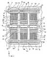
図1はこの発明の一実施の形態に係るMESFET素子の平面図である。図2は図1のA部におけるMESFET素子の部分拡大平面図である。図3は図2のB部におけるMESFET素子の一部破断平面図である。図4は図2のVI−VI断面におけるMESFET素子の部分断面図であり、図5は図2のV−V断面におけるMESFET素子の部分断面図である。
図1において、MESFET素子10は、半導体基板12上に、複数の単位MESFETが図のx軸方向に並列に配置された半導体素子群としての単位MESFET群(以下、セルという。)14(14a、14b、14c、・・・)がx軸方向に、例えば6個配設され、この6個のセル12がy軸方向に、例えば2段配設されている。セルの数は必要とされる出力の大きさによって決定される。
第1の半導体素子群としての第1セル14aと第2の半導体素子群としての第2セル14bとは第1セル14aのゲート電極の延長方向であるy軸方向に並べて配置されている。第3の半導体素子群としての第3セル14cと第4の半導体素子群としての第4セル14dとは第3セル14cのゲート電極の延長方向であるy軸方向に並べて配置されるとともに、第1セル14aと第2セル14bに対して適宜間隔を置いてx軸方向に隣接して並置されている。Embodiment 1 FIG.
FIG. 1 is a plan view of a MESFET device according to an embodiment of the present invention. FIG. 2 is a partially enlarged plan view of the MESFET element in section A of FIG. FIG. 3 is a partially broken plan view of the MESFET element in part B of FIG. 4 is a partial cross-sectional view of the MESFET element in the VI-VI cross section of FIG. 2, and FIG. 5 is a partial cross-sectional view of the MESFET element in the VV cross section of FIG.
In FIG. 1, a
The
y軸方向に隣接する二つのセル14の間にゲート電極接続配線としてのゲート電極バー16が配設されていて、第1セル14aと第2セル14bとの間、および第3セル14cと第4セル14dとの間に、第1のゲート電極接続配線としてのゲート電極バー16aが配設されている。ゲート電極バー16aには第1セル14a、第2セル14b、第3セル14c、および第4セル14d各々の各単位MESFETのゲート電極が接続されている。 このゲート電極バー16の中央にワイヤを接続するためのボンディングパッド18が配設されている。
第1セル14aおよび第2セル14bの側部で、第3セル14cと第4セル14dとが並置された側部と反対側の側部には、第5の半導体素子群としての第5セル14eと第6の半導体素子群としての第6セル14fとがゲート電極の延長方向であるy軸方向に並べて配置されるとともに、第1セル14aと第2セル14bに対して適宜間隔を置いて配置されている。第5セル14eと第6セル14fとの間に、第2のゲート電極接続配線としてのゲート電極バー16bが配設されている。ゲート電極バー16bには第5セル14eと第6セル14fそれぞれの各単位MESFETのゲート電極が接続されるとともに、第5セル14eと第6セル14fの外側にさらに隣接する二つのセル各々の各単位MESFETのゲート電極が接続されている。A
On the side opposite to the side where the
各セル14において、各単位MESFETのゲート電極バー16に近接する側の端部、即ち第2の端部としての内端部には、第2の電極としての例えばソース電極とゲート電極とを跨ぎ、第1の電極としての例えばドレイン電極を接続する、第1電極接続配線としてのドレイン電極接続配線20が配設されている。
第1セル14a、第2セル14b、第5セル14e、および第6セル14fの各ドレイン接続配線20は、第1セル14aと第5セル14eとの間および第2セル14bと6セル14fとの間に延在するように配設された第1電極引出配線としてのドレイン電極引出線22に接続されている。ドレイン電極引出線22の中央にワイヤを接続するためのボンディングパッド24が配設されている。
各セル14において、各単位MESFETのゲート電極バー16に対して外側の端部、即ち第1の端部としての外端部には、第1の電極としての例えばドレイン電極とゲート電極とを跨ぎ、第2の電極としての例えばソース電極を接続する第2電極接続配線としてのソース電極接続配線26が配設されている。この各ソース電極接続配線26はソースパッド27で接続され、ソースパッド27はバイアホール(Via Hole)28を介して半導体基板12の裏面に配設された金属膜で形成されたPHS(Plated Heat Sink)に接続され、ソース接地の場合に接地される。In each
The drain connection wirings 20 of the
In each
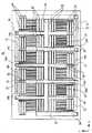
次に図2によりセル14について説明する。
図2において、単位MESFET30はドレイン電極32、ゲート電極34,およびソース電極36から構成され、互いに隣接する一つの単位MESFET30は左右に隣接する単位MESFET30と互いにドレイン電極32またはソース電極36を共有している。ゲート電極の間隔は例えば20μm程度である。
図2のセルにおいては図を分かり易くするために、図1のセルより単位MESFET30の数を少なくして描いている。またドレイン電極32とソース電極36とを区別しやすいように異なる傾きの斜線を描いているが、この斜線は断面を示すものではない。
一つのセル14に含まれる単位MESFET30の数は、許容される熱抵抗の値から決まり、一つのセルでゲート電極が、例えば12本程度配設され、12個の単位MESFET30で一つのセルが構成されている。一つのセルにあまり多くの単位MESFET30を含めると熱抵抗が増大し各セル間での均一動作が阻害されて、MESFET素子の出力特性が劣化する。Next, the
In FIG. 2, a
In the cell of FIG. 2, the number of
The number of
単位MESFET30においてゲート幅はy軸方向の長さであり、例えば800μm程度である。従ってMESFET素子10に出力を増加させるためには、単位MESFET30のゲート電極34のy軸方向の長さをゲート抵抗の増加が利得の低下を招かない程度にできるだけ長くするとともに、単位MESFET30の数を増やす必要がある。しかもチップ形状が大きくならないことが要求される。
この実施の形態では、ゲート抵抗の増加が利得の低下を招かない程度に長くしたゲート電極を有する単位MESFET30を、許容される熱抵抗の値から決まる個数だけ並置したセル14を構成することにより、熱抵抗が増大することを抑制しながら出力の増加を図り、チップのy軸方向に2段に配置し、4個のセル、例えばセル14aと14bの間、および14cと14dとの間に一つのゲート電極バー16aをx軸方向に延在させて、セル14a、14b、14c、および14dのゲート電極34を接続し、4個のセルで一つのゲート電極バー16aを共有することにより、y軸方向のチップ長さを短くしている。
またゲート電極バー16aに対して各セルの外側、すなわち基板12のチップ辺縁12aに近い側において、各単位MESFET30のドレイン電極32とゲート電極34とを跨ぎ、ソース電極36を接続する、いわゆるエアブリッジとしたソース電極接続配線26が配設されている。
さらに、ゲート電極バー16aに近接する各セルの内側、すなわちゲート電極バー16aに近接した基板の中央側に、各単位MESFET30のソース電極36とゲート電極34とを跨ぎ、ドレイン電極32を接続する、いわゆるエアブリッジとしたドレイン電極接続配線20が配設されている。In the
In this embodiment, by constructing
Further, on the outside of each cell, that is, on the side close to the
Further, the
図3および図4に示されるように、ソース電極接続配線26はエアブリッジ構造で、各単位MESFET30の外端部でドレイン電極32とゲート電極34とをエアギャップを介して跨ぎ、ソース電極36の表面においてソース電極36と、また基板12表面にソースパッド27を介して接続されている。ソース電極接続配線26とソースパッド27とはこの実施の形態においてはAuメッキ層で一体的に公知の製造方法によって形成される。
図5に示されるようにドレイン電極接続配線20もソース電極接続配線26と同様のエアブリッジ構造で、各単位MESFET30の内端部でソース電極36とゲート電極34とをエアギャップを介して跨ぎ、ドレイン電極32の表面においてドレイン電極32と接続され、基板12表面とはドレイン電極引出線22を介して接続されている。ドレイン電極接続配線20とドレイン電極引出線22とは、この実施の形態においては、Auメッキ層で一体的に公知の製造方法によって形成される。
このエアブリッジ構造は、ソース電極接続配線26およびドレイン電極接続配線20のy軸方向の幅を比較的広くしながら、エアブリッジ構造を形成しやすくするために、それぞれ平行する3分割の接続配線構造になっている。ソース電極接続配線26およびドレイン電極接続配線20それぞれのy軸方向の幅は200μm、つまりソース電極接続配線26の3分割された接続配線の幅を合わせた総幅が概ね200μm程度であり、またドレイン電極接続配線20の3分割された接続配線の幅を合わせた総幅が概ね200μm程度となっている。As shown in FIG. 3 and FIG. 4, the source
As shown in FIG. 5, the drain
In this air bridge structure, the source
従ってソース電極接続配線26およびドレイン電極接続配線20が各単位MESFET30の上に形成されたエアブリッジ構造をとることにより、y軸方向のチップ長さを短くするとともに、ソース電極接続配線26およびドレイン電極接続配線20それぞれのインダクタンスを小さくすることが出来る。この低インダクタンス化により、高周波用MESFET10の高利得化が達成でき、高周波特性を向上させることにより高速性を高めている。
図4および図5に示されるように、半導体基板12はGaAsからなる基板本体12bと基板本体12b表面上に形成された動作領域としてのGaAsのエピタキシャル層12cとから形成され、半導体基板12の裏面にはAuメッキ層からなるPHS40が形成されている。エピタキシャル層12cの表面に、ゲート電極34が整流接続され、ドレイン電極32とソース電極36とがオーミックに接続されている。
ゲート電極バー16は公知の製造方法を用い、Auメッキ層により形成されている。
この実施の形態においては、動作領域は、GaAsのエピタキシャル層12cにより形成されているが、GaAs基板に不純物を注入することにより形成してもよい。Therefore, by adopting an air bridge structure in which the source
As shown in FIGS. 4 and 5, the
The
In this embodiment, the operating region is formed by the
図2において、さらに第5セル14eと第6セル14fとを第1セル14aと第2セル14bの側部に隣接して配置し、ゲート電極バー16bに第5セル14eと第6セル14fとの各単位MESFETのゲート電極を接続し、第5セル14e、第6セル14fそれぞれのソース電極接続配線26を隣接する第1セル14a、第2セル14bのソース電極接続配線26とソースパッド27を介して接続するとともに、第5セル14e、第6セル14fそれぞれのドレイン電極引出線22を、第1セル14aと第5セル14eとの間および第2セル14bと6セル14fとの間に配設されたドレイン電極引出線22に接続している。
このように、例えば第1セル14a、第2セル14b、第3セル14cおよび第4セル14dの4セルからなる第1のセル群でゲート電極バー16bを共有し、かつ第1セル14a、第2セル14b、第5セル14eおよび第6セル14fの4セルからなる第2のセル群の電極接続配線20に接続されたドレイン電極引出線22を共有することにより、ゲート電極バー16bのボンディングパッド18とドレイン電極引出線22のボンディングパッド24とをチップ中央のチップ長手方向、つまりx軸方向に、交互に均等に配置することができ、信号の伝達を均一に行うことができる。
またボンディングパッド18およびボンディングパッド24はそれぞれ、半導体基板上に配設されたゲート電極バー16およびドレイン電極引出線22の上に形成され、エアブリッジ構造の上に形成されたボンディングパッド18およびボンディングパッド24に比べて、ワイヤボンディングに際しても単位MESFET30が機械的な損傷を被ることはない。In FIG. 2, a
Thus, for example, the first cell group consisting of four cells of the
以上のように、この実施の形態に係るMESFET素子10は、所定の個数の単位MESFET30からなるセルを基本に分散配置され、熱抵抗の増大を抑制することにより、出力増加を図ることができ、高出力化が可能になる。
またゲート電極バー16bのボンディングパッド18とドレイン電極引出線22のボンディングパッド24とをチップ中央のチップ長手方向に交互に均等に配置することができ、信号を均一に伝達することができる。
さらに、ゲート電極バー16がチップのy軸方向中央に配設することにより、ゲート電極バー16を挟んで両側に配設されたセル14においてゲート電極バー16bを共有することができ、またソース電極接続配線26およびドレイン電極接続配線20が各単位MESFET30上でエアブリッジ構造をなすことにより、y軸方向のチップ長さを短くすることができ、MESFET素子10を小形化することができる。
さらにまたソース電極接続配線26およびドレイン電極接続配線20が各単位MESFET30上でエアブリッジ構造をなすので、ソース電極接続配線26およびドレイン電極接続配線20のy軸方向の幅を比較的広くすることができる。このためそれぞれのインダクタンスを小さくすることができ、高利得化が可能になり、また素子の高周波特性が向上し高速化を図ることができる。As described above, the
Further, the
Further, by disposing the
Furthermore, since the source
また、ソース電極接続配線26およびドレイン電極接続配線20が各単位MESFET30上でエアブリッジ構造をなすことにより、絶縁膜を介してソース電極接続配線およびドレイン電極接続配線を配設する場合に比べてキャパシタンスが小さくなり、高速性能を高めることができる。
延いては、高出力で、利得の低下が少なく、高速性能にすぐれた高周波用半導体装置を構成することができる。Further, since the source
As a result, it is possible to configure a high-frequency semiconductor device that has high output, little gain reduction, and excellent high-speed performance.
図6はこの発明の一実施の形態に係るMESFET素子の変形例の平面図である。
図6において、図1〜図5と同じ符号は同じものか相当のものを示す。なお以下の各図においても同様である。
図6において、MESFET素子50は、MESFET素子10においてゲート電極バー16を共有する4個のセル、たとえば第1セル14a、第2セル14b、第3セル14cおよび第4セル14dの4セルからなるセル群の、第1セル14aと第3セル14c、および第2セル14bと第4セル14dにおいて、ソースパッド27を削除して第1セル14aと第3セル14cとの間、および第2セル14bと第4セル14dとの間に設けられた間隔を無くするとともに隣り合った単位MESFET30を交互につなぎ合わせた配置にしたものである。他の構成はMESFET素子10と同様である。
この構成をとることにより、さらにチップの長手方向、即ち、x軸方向の長さを短縮することが出来る。FIG. 6 is a plan view of a modification of the MESFET device according to one embodiment of the present invention.
In FIG. 6, the same reference numerals as those in FIGS. The same applies to the following drawings.
In FIG. 6, the
By adopting this configuration, the length of the chip, that is, the length in the x-axis direction can be further shortened.
実施の形態2.
図7はこの発明の一実施の形態に係るMESFET素子の平面図である。
図7において、MESFET素子60は、MESFET素子10においてゲート電極バー16を共有する4個のセル、たとえば第1セル14a、第2セル14b、第3セル14cおよび第4セル14dの4セルからなるセル群の、第1セル14aと第3セル14cとのソース電極接続配線26を接続するソースパッド27を削除するとともに、第1セル14aと第3セル14cとの間を、第1セル14aおよび第3セル14cの側部に沿ってゲート電極バー16aをy軸方向に、第1セル14aおよび第3セル14cの外端部まで延長し、図7においては逆T字状に形成したゲート電極バー16aの延長部16aを設け、この延長部16aの外端部にボンディングパッド18を形成している。Embodiment 2. FIG.
FIG. 7 is a plan view of a MESFET device according to an embodiment of the present invention.
In FIG. 7, the
さらにドレイン電極引出線22を共有する4個のセル、たとえば第1セル14a、第2セル14b、第5セル14eおよび第6セル14fからなるセル群の、第2セル14bと第6セル14fとのソース電極接続配線26を接続するソースパッド27を削除するとともに、ドレイン電極引出線22を第2セル14bおよび第6セル14fの側部に沿ってゲート電極バー16aが延長された方向と逆方向のy軸方向に、第2セル14bおよび第6セル14fの外端部まで延長し、このドレイン電極引出線22の延長部22aを設け、この延長部22aの外端部にボンディングパッド24を設けたものである。
即ち実施の形態1のMESFET素子10ではチップ中央の一線上に交互に、ゲート電極バー16aのボンディングパッド18とドレイン電極引出線22のボンディングパッド24とが配設されたのに対して、MESFET素子60ではチップ中央のx軸に対して逆方向に位置する一方のチップ辺縁にはゲート電極バー16aのボンディングパッド18を、また他方のチップ辺縁にはドレイン電極引出線22のボンディングパッド24を配設したものである。Further, the four cells sharing the drain
That is, in the
以上のようにこの構成のMESFET素子60においては、実施の形態1のMESFET素子10の効果に加えて、パッケージの基板にMESFET素子60を組み立てたときに、同じくパッケージの基板上に配設される入力整合回路または出力整合回路とのボンディングワイヤを短くすることができる。このためにインダクタンスが小さくなり、インピーダンス整合のバラツキが少なくなり、電気的特性の揃った高周波半導体装置を構成することができ、また歩留まりを高くすることができる。延いては電気的特性がよく安価な高周波用半導体装置を得ることができる。 As described above, in addition to the effects of the
図8はこの発明の一実施の形態に係るMESFET素子の変形例の平面図である。
図8において、MESFET素子70は、上述のMESFET素子60におけるゲート電極バー16を、ゲート電極バー16の両側のセル14、例えば第1セル14aおよび第3セル14cの側部に沿った延長部16aをセル14の外端部を越えてさらに延長し、さらにチップ辺縁12aに近づけ、またドレイン電極引出線22を、ドレイン電極引出線22の両側のセル、例えば第2セル14bおよび第6セル14fの側部に沿って延長部22aをセル14の外端部を越えてさらに延長しチップ辺縁12aに近づけるとともに、隣接するゲート電極バー16の延長部16aの間、および隣接するドレイン電極引出線22の延長部22aの間に、それぞれに発信抑制回路72、例えば抵抗を有する電極接続配線を配設し、ゲート電極バー16のボンディングパッド18およびドレイン電極引出線22のボンディングパッド24と接続するものである。
これによりセル14間の発振を抑制することができる。
以上の実施の形態においては、ゲート電極バー16に近接して、ドレイン電極接続配線20を設け、ゲート電極バー16に対して外側のチップ辺縁にソース電極接続配線26を設ける場合に説明したが、これとは逆にゲート電極バー16に近接してソース電極接続配線を設け、ゲート電極バー16に対して外側のチップ辺縁にドレイン電極接続配線を設ける構成としても、同様の効果を奏する。なお、上述の説明では、各実施の形態の一例としてMESFETを用いて説明したが、他の高周波用FET、例えばHEMT、HFETおよびMOSFETなどにおいても同様の効果を奏する。FIG. 8 is a plan view of a modification of the MESFET device according to one embodiment of the present invention.
In FIG. 8, the
Thereby, oscillation between the
In the above embodiment, the drain
以上のように、この発明に係る高周波用半導体装置は、衛星通信や移動体通信用送受信機器などの通信機器に使用される高出力増幅器などの高周波用半導体装置に適している。As described above, the high-frequency semiconductor device according to the present invention is suitable for a high-frequency semiconductor device such as a high-power amplifier used in communication equipment such as satellite communication and mobile communication transceiver equipment.
12 基板、 12c エピタキシャル層、 34 ゲート電極、 32 ドレイン電極、 36 ソース電極、 26 ソース電極接続配線、 20 ドレイン電極接続配線、 14a 第1セル、 14b 第2セル、 16a ゲート電極バー、 22 ドレイン電極引出線、 14c 第3セル、 14d 第4セル14d、 14e 第5セル、 14f 第6セル、 16b ゲート電極バー。 12 substrate, 12c epitaxial layer, 34 gate electrode, 32 drain electrode, 36 source electrode, 26 source electrode connection wiring, 20 drain electrode connection wiring, 14a first cell, 14b second cell, 16a gate electrode bar, 22 drain electrode extraction Line, 14c 3rd cell, 14d
Claims (5)
Translated fromJapaneseこの基板の活性領域の表面に配設されゲート幅の方向に延長されそれぞれ互いに並置された複数のゲート電極、これらのゲート電極に並行して延在し上記活性領域の表面にオーミックに接続され順次ゲート電極を介して一つずつ交互に配設されたそれぞれ複数の第1の電極と第2の電極、上記各ゲート電極および各第1の電極および各第2の電極の同じ側の第1の端部において上記各ゲート電極と各第1の電極とを跨ぎ上記各第2の電極を接続した第2電極接続配線、並びに上記各ゲート電極および各第1の電極および各第2の電極の第2の端部において上記各ゲート電極と各第2電極とを跨ぎ上記各第1の電極を接続した第1電極接続配線を有する第1の半導体素子群と、
この第1の半導体素子群と同じ構成を有し上記第1の半導体素子群の各ゲート電極の延長方向に配設されるとともに、上記第1の半導体素子群の第1電極接続配線に近接して第1電極接続配線が配設された第2の半導体素子群と、
上記第1、第2の半導体素子群それぞれの第1電極接続配線の間の上記基板上に配設されるとともに、上記第1、第2の半導体素子群の各ゲート電極の第2の端部が接続された第1のゲート電極接続配線と、
を備えた高周波用半導体装置。A substrate having an active region on a first major surface;
A plurality of gate electrodes arranged on the surface of the active region of the substrate, extending in the direction of the gate width and juxtaposed to each other, and extending in parallel to the gate electrodes and being ohmically connected to the surface of the active region. A plurality of first electrodes and second electrodes, which are alternately arranged one by one via the gate electrodes, the first electrodes on the same side of the gate electrodes, the first electrodes, and the second electrodes, respectively. A second electrode connection wiring connecting the second electrodes across the gate electrodes and the first electrodes at the end, and the gate electrodes, the first electrodes, and the second electrodes of the second electrodes; A first semiconductor element group having a first electrode connection wiring connecting the first electrodes across the gate electrodes and the second electrodes at two ends;
The first semiconductor element group has the same configuration and is disposed in the extending direction of each gate electrode of the first semiconductor element group, and is close to the first electrode connection wiring of the first semiconductor element group. A second semiconductor element group in which the first electrode connection wiring is disposed;
A second end portion of each gate electrode of the first and second semiconductor element groups is disposed on the substrate between the first electrode connection wirings of the first and second semiconductor element groups. A first gate electrode connection wiring to which is connected;
A high-frequency semiconductor device comprising:
Priority Applications (2)
| Application Number | Priority Date | Filing Date | Title |
|---|---|---|---|
| JP2003424335AJP2005183770A (en) | 2003-12-22 | 2003-12-22 | High frequency semiconductor devices |
| US10/995,133US20050133829A1 (en) | 2003-12-22 | 2004-11-24 | High-frequency semiconductor device |
Applications Claiming Priority (1)
| Application Number | Priority Date | Filing Date | Title |
|---|---|---|---|
| JP2003424335AJP2005183770A (en) | 2003-12-22 | 2003-12-22 | High frequency semiconductor devices |
Publications (1)
| Publication Number | Publication Date |
|---|---|
| JP2005183770Atrue JP2005183770A (en) | 2005-07-07 |
Family
ID=34675390
Family Applications (1)
| Application Number | Title | Priority Date | Filing Date |
|---|---|---|---|
| JP2003424335APendingJP2005183770A (en) | 2003-12-22 | 2003-12-22 | High frequency semiconductor devices |
Country Status (2)
| Country | Link |
|---|---|
| US (1) | US20050133829A1 (en) |
| JP (1) | JP2005183770A (en) |
Cited By (2)
| Publication number | Priority date | Publication date | Assignee | Title |
|---|---|---|---|---|
| WO2020100219A1 (en)* | 2018-11-13 | 2020-05-22 | 三菱電機株式会社 | High-frequency amplifier and high-frequency amplifier module |
| WO2025062576A1 (en)* | 2023-09-21 | 2025-03-27 | 株式会社 東芝 | Semiconductor device |
Families Citing this family (21)
| Publication number | Priority date | Publication date | Assignee | Title |
|---|---|---|---|---|
| US7456476B2 (en) | 2003-06-27 | 2008-11-25 | Intel Corporation | Nonplanar semiconductor device with partially or fully wrapped around gate electrode and methods of fabrication |
| US7042009B2 (en) | 2004-06-30 | 2006-05-09 | Intel Corporation | High mobility tri-gate devices and methods of fabrication |
| US20060086977A1 (en) | 2004-10-25 | 2006-04-27 | Uday Shah | Nonplanar device with thinned lower body portion and method of fabrication |
| US7518196B2 (en) | 2005-02-23 | 2009-04-14 | Intel Corporation | Field effect transistor with narrow bandgap source and drain regions and method of fabrication |
| US7858481B2 (en) | 2005-06-15 | 2010-12-28 | Intel Corporation | Method for fabricating transistor with thinned channel |
| US7547637B2 (en) | 2005-06-21 | 2009-06-16 | Intel Corporation | Methods for patterning a semiconductor film |
| US7279375B2 (en)* | 2005-06-30 | 2007-10-09 | Intel Corporation | Block contact architectures for nanoscale channel transistors |
| US20070090416A1 (en) | 2005-09-28 | 2007-04-26 | Doyle Brian S | CMOS devices with a single work function gate electrode and method of fabrication |
| US7485503B2 (en) | 2005-11-30 | 2009-02-03 | Intel Corporation | Dielectric interface for group III-V semiconductor device |
| US8143646B2 (en) | 2006-08-02 | 2012-03-27 | Intel Corporation | Stacking fault and twin blocking barrier for integrating III-V on Si |
| US7678632B2 (en)* | 2006-11-17 | 2010-03-16 | Infineon Technologies Ag | MuGFET with increased thermal mass |
| JP2009267347A (en)* | 2008-03-31 | 2009-11-12 | Toshiba Corp | Semiconductor device and manufacturing method thereof |
| US8362566B2 (en) | 2008-06-23 | 2013-01-29 | Intel Corporation | Stress in trigate devices using complimentary gate fill materials |
| DE102010001788A1 (en)* | 2010-02-10 | 2011-08-11 | Forschungsverbund Berlin e.V., 12489 | Scalable structure for lateral semiconductor devices with high current carrying capacity |
| CN105206590B (en)* | 2015-09-17 | 2017-11-03 | 浙江大学 | PHEMT Microwave Power Amplifier tube core transversaries and pHEMT that air bridges side is drawn |
| US10763334B2 (en) | 2018-07-11 | 2020-09-01 | Cree, Inc. | Drain and/or gate interconnect and finger structure |
| US10600746B2 (en) | 2018-07-19 | 2020-03-24 | Cree, Inc. | Radio frequency transistor amplifiers and other multi-cell transistors having gaps and/or isolation structures between groups of unit cell transistors |
| US10770415B2 (en) | 2018-12-04 | 2020-09-08 | Cree, Inc. | Packaged transistor devices with input-output isolation and methods of forming packaged transistor devices with input-output isolation |
| US11417746B2 (en) | 2019-04-24 | 2022-08-16 | Wolfspeed, Inc. | High power transistor with interior-fed fingers |
| JP2023122726A (en)* | 2022-02-24 | 2023-09-05 | 住友電工デバイス・イノベーション株式会社 | Semiconductor device |
| CN117558749B (en)* | 2024-01-11 | 2024-05-03 | 英诺赛科(珠海)科技有限公司 | A gallium nitride device structure |
Family Cites Families (3)
| Publication number | Priority date | Publication date | Assignee | Title |
|---|---|---|---|---|
| JPH04252036A (en)* | 1991-01-10 | 1992-09-08 | Fujitsu Ltd | Semiconductor device |
| JP3269475B2 (en)* | 1998-02-16 | 2002-03-25 | 日本電気株式会社 | Semiconductor device |
| JP3712111B2 (en)* | 2001-03-30 | 2005-11-02 | ユーディナデバイス株式会社 | Power amplification semiconductor device |
- 2003
- 2003-12-22JPJP2003424335Apatent/JP2005183770A/enactivePending
- 2004
- 2004-11-24USUS10/995,133patent/US20050133829A1/ennot_activeAbandoned
Cited By (2)
| Publication number | Priority date | Publication date | Assignee | Title |
|---|---|---|---|---|
| WO2020100219A1 (en)* | 2018-11-13 | 2020-05-22 | 三菱電機株式会社 | High-frequency amplifier and high-frequency amplifier module |
| WO2025062576A1 (en)* | 2023-09-21 | 2025-03-27 | 株式会社 東芝 | Semiconductor device |
Also Published As
| Publication number | Publication date |
|---|---|
| US20050133829A1 (en) | 2005-06-23 |
Similar Documents
| Publication | Publication Date | Title |
|---|---|---|
| JP2005183770A (en) | High frequency semiconductor devices | |
| US6900482B2 (en) | Semiconductor device having divided active regions with comb-teeth electrodes thereon | |
| JP7614953B2 (en) | Transistor with I/O port within active area of the transistor - Patents.com | |
| US5883407A (en) | Semiconductor device | |
| EP2088620B1 (en) | Semiconductor device | |
| EP2515435B1 (en) | Power amplifier | |
| WO2017163612A1 (en) | Power semiconductor module | |
| JP2001028425A (en) | Semiconductor device and manufacturing method thereof | |
| US20080217770A1 (en) | Mounting configuration of electronic component | |
| JP4025044B2 (en) | Semiconductor integrated circuit device | |
| US20230268343A1 (en) | Semiconductor device | |
| EP4273925A1 (en) | Packaged electronic device comprising a plurality of power transistors | |
| JP2010183100A (en) | Semiconductor amplifier | |
| JP6849060B2 (en) | amplifier | |
| JP5550224B2 (en) | Semiconductor device | |
| CN101371345B (en) | High-frequency semiconductor device | |
| JP7456517B2 (en) | transistor | |
| US7042053B2 (en) | Semiconductor device with polymer insulation of some electrodes | |
| EP0905791A2 (en) | Miniaturization of a semiconductor chip | |
| JP4579040B2 (en) | Semiconductor amplifier | |
| JPH09232334A (en) | Compound semiconductor | |
| JP2013105978A (en) | High-frequency semiconductor device | |
| US20230102118A1 (en) | Semiconductor device | |
| KR101958568B1 (en) | Semiconductor device | |
| KR20240140232A (en) | Semiconductor device and power amplifier including the same |