JP2005174977A - Ferroelectric memory device and manufacturing method thereof - Google Patents
Ferroelectric memory device and manufacturing method thereofDownload PDFInfo
- Publication number
- JP2005174977A JP2005174977AJP2003408646AJP2003408646AJP2005174977AJP 2005174977 AJP2005174977 AJP 2005174977AJP 2003408646 AJP2003408646 AJP 2003408646AJP 2003408646 AJP2003408646 AJP 2003408646AJP 2005174977 AJP2005174977 AJP 2005174977A
- Authority
- JP
- Japan
- Prior art keywords
- film
- ferroelectric
- diffusion layer
- groove
- insulating film
- Prior art date
- Legal status (The legal status is an assumption and is not a legal conclusion. Google has not performed a legal analysis and makes no representation as to the accuracy of the status listed.)
- Pending
Links
Images


Classifications
- H—ELECTRICITY
- H10—SEMICONDUCTOR DEVICES; ELECTRIC SOLID-STATE DEVICES NOT OTHERWISE PROVIDED FOR
- H10B—ELECTRONIC MEMORY DEVICES
- H10B51/00—Ferroelectric RAM [FeRAM] devices comprising ferroelectric memory transistors
- H10B51/30—Ferroelectric RAM [FeRAM] devices comprising ferroelectric memory transistors characterised by the memory core region
- H—ELECTRICITY
- H10—SEMICONDUCTOR DEVICES; ELECTRIC SOLID-STATE DEVICES NOT OTHERWISE PROVIDED FOR
- H10B—ELECTRONIC MEMORY DEVICES
- H10B12/00—Dynamic random access memory [DRAM] devices
- H10B12/01—Manufacture or treatment
- H10B12/02—Manufacture or treatment for one transistor one-capacitor [1T-1C] memory cells
- H10B12/05—Making the transistor
- H10B12/053—Making the transistor the transistor being at least partially in a trench in the substrate
- H—ELECTRICITY
- H10—SEMICONDUCTOR DEVICES; ELECTRIC SOLID-STATE DEVICES NOT OTHERWISE PROVIDED FOR
- H10B—ELECTRONIC MEMORY DEVICES
- H10B51/00—Ferroelectric RAM [FeRAM] devices comprising ferroelectric memory transistors
- H—ELECTRICITY
- H10—SEMICONDUCTOR DEVICES; ELECTRIC SOLID-STATE DEVICES NOT OTHERWISE PROVIDED FOR
- H10B—ELECTRONIC MEMORY DEVICES
- H10B53/00—Ferroelectric RAM [FeRAM] devices comprising ferroelectric memory capacitors
- H—ELECTRICITY
- H10—SEMICONDUCTOR DEVICES; ELECTRIC SOLID-STATE DEVICES NOT OTHERWISE PROVIDED FOR
- H10B—ELECTRONIC MEMORY DEVICES
- H10B12/00—Dynamic random access memory [DRAM] devices
- H10B12/30—DRAM devices comprising one-transistor - one-capacitor [1T-1C] memory cells
- H10B12/31—DRAM devices comprising one-transistor - one-capacitor [1T-1C] memory cells having a storage electrode stacked over the transistor
- H10B12/318—DRAM devices comprising one-transistor - one-capacitor [1T-1C] memory cells having a storage electrode stacked over the transistor the storage electrode having multiple segments
- H—ELECTRICITY
- H10—SEMICONDUCTOR DEVICES; ELECTRIC SOLID-STATE DEVICES NOT OTHERWISE PROVIDED FOR
- H10B—ELECTRONIC MEMORY DEVICES
- H10B12/00—Dynamic random access memory [DRAM] devices
- H10B12/30—DRAM devices comprising one-transistor - one-capacitor [1T-1C] memory cells
- H10B12/34—DRAM devices comprising one-transistor - one-capacitor [1T-1C] memory cells the transistor being at least partially in a trench in the substrate
Landscapes
- Engineering & Computer Science (AREA)
- Manufacturing & Machinery (AREA)
- Semiconductor Memories (AREA)
Abstract
Translated fromJapaneseDescription
Translated fromJapanese本発明は、強誘電体キャパシタを有する強誘電体記憶装置及びその製造方法に関する。 The present invention relates to a ferroelectric memory device having a ferroelectric capacitor and a method for manufacturing the same.
近年、不揮発性半導体メモリの一つとして、強誘電体キャパシタを用いた強誘電体メモリ(FeRAM:Ferro-electric Random Access Memory)が注目されている。このFeRAMでは、従来から、1つのトランジスタ(Tr)と1つの強誘電体キャパシタ(C)とで1セルが構成される1Tr+1C型が提案されている。 In recent years, a ferroelectric memory (FeRAM: Ferro-electric Random Access Memory) using a ferroelectric capacitor has attracted attention as one of nonvolatile semiconductor memories. For this FeRAM, a 1Tr + 1C type in which one cell is composed of one transistor (Tr) and one ferroelectric capacitor (C) has been proposed.
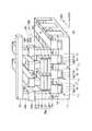
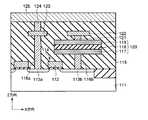
図69乃至図72は、従来技術による1Tr+1C型のFeRAMの概略的なセル構造を示す。図69乃至図72に示すように、半導体基板111上にゲート電極112が形成され、このゲート電極112の両側に一対のソース/ドレイン拡散層113a,113bが形成されることで、トランジスタ114が形成されている。このトランジスタ114上には層間絶縁膜115が形成され、この層間絶縁膜115内にはソース/ドレイン拡散層113a,113bに接続するコンタクト116a,116bが形成されている。そして、一方のコンタクト116b上には、下部電極117、強誘電体膜118及び上部電極119からなる強誘電体キャパシタ120が接続され、上部電極119上には、コンタクト121を介してプレート線122が形成されている。他方のコンタクト116a上には、配線123及びコンタクト124を介してビット線125が接続されている。 69 to 72 show a schematic cell structure of a 1Tr + 1C type FeRAM according to the prior art. As shown in FIGS. 69 to 72, a
ここで、図70のセルは、強誘電体キャパシタ120を構成する下部電極117、強誘電体膜118及び上部電極119がXY方向にのみ平面的に延在しており、半導体基板面と水平な面のみがキャパシタ面として利用する2次元キャパシタを備えている。また、図71及び図72のセルは、強誘電体キャパシタ120を構成する下部電極117、強誘電体膜118及び上部電極119の少なくとも一部がXYZ方向に立体的に延在しており、半導体基板面と水平な面のみならず、下部電極117の半導体基板面に対して水平でない側面部分をキャパシタ面として利用する3次元キャパシタを備えている。 Here, in the cell of FIG. 70, the
上記のような従来のセル構造において、ビット線125と半導体基板111との間には、強誘電体キャパシタ120、プレート線122、強誘電体キャパシタ120とトランジスタ114とを接続するコンタクト116b、強誘電体キャパシタ120とプレート線122とを接続するコンタクト121、ビット線125とトランジスタ114とを接続する配線123及びコンタクト116a,124などが存在する。従って、ビット線125と半導体基板111との間の層間絶縁膜115の膜厚が厚くなるため、ビット線125と半導体基板111とを接続するコンタクトが非常に深くなる。特に、メモリの微細化によって、このコンタクトの径は0.15〜0.18μm径程度にますます小さくなり、コンタクトのアスペクト比が高くなってしまうため、サイズを保持しつつ良好なコンタクトを形成することがさらに困難になってくると予測される。 In the conventional cell structure as described above, between the
本発明は上記課題を解決するためになされたものであり、その目的とするところは、ビット線とトランジスタとを接続するコンタクトのアスペクト比を低減させることが可能な強誘電体記憶装置及びその製造方法を提供することにある。 The present invention has been made to solve the above-described problems, and an object of the present invention is to provide a ferroelectric memory device capable of reducing the aspect ratio of a contact connecting a bit line and a transistor, and its manufacture. It is to provide a method.
本発明は、前記目的を達成するために以下に示す手段を用いている。 In order to achieve the above object, the present invention uses the following means.
本発明の第1の視点による強誘電体記憶装置は、半導体基板と、前記半導体基板内に第1の方向に延在して形成され、第1の深さを有する第1の溝と、前記半導体基板内に前記第1の溝を横切る第2の方向に延在して形成され、前記第1の深さより浅い第2の深さを有し、上部領域と下部領域とを備えた第2の溝と、前記第1の溝内に埋め込まれた第1の素子分離絶縁膜と、前記第2の溝の前記下部領域内に第1のゲート絶縁膜を介して形成された第1のゲート電極と、前記第2の溝の前記上部領域内に形成された第1の絶縁膜と、前記第2の溝における一方の側面側の前記半導体基板内に形成された第1の拡散層と、前記第2の溝における他方の側面側の前記半導体基板内に形成された第2の拡散層と、前記第1の拡散層上に配置され、第1の下部電極と第1の強誘電体膜と第1の上部電極とを有する第1の強誘電体キャパシタと、前記第1の強誘電体キャパシタ上に配置された第1のコンタクトと、前記第1のコンタクト上に配置された第1の配線層と、前記第2の拡散層上に配置された第2のコンタクトと、前記第2のコンタクト上に配置され、第1の配線層と同一レベルに配置された第2の配線層とを具備する。 A ferroelectric memory device according to a first aspect of the present invention includes a semiconductor substrate, a first groove formed in the semiconductor substrate so as to extend in a first direction and having a first depth, A second extension formed in the semiconductor substrate extending in a second direction across the first trench, having a second depth shallower than the first depth, and comprising an upper region and a lower region. , A first element isolation insulating film embedded in the first groove, and a first gate formed in the lower region of the second groove via a first gate insulating film An electrode, a first insulating film formed in the upper region of the second groove, a first diffusion layer formed in the semiconductor substrate on one side surface of the second groove, A second diffusion layer formed in the semiconductor substrate on the other side of the second groove, and disposed on the first diffusion layer, A first ferroelectric capacitor having a lower electrode, a first ferroelectric film, and a first upper electrode; a first contact disposed on the first ferroelectric capacitor; A first wiring layer disposed on one contact, a second contact disposed on the second diffusion layer, and the same level as the first wiring layer disposed on the second contact. And a second wiring layer disposed on the substrate.
本発明の第2の視点による強誘電体記憶装置の製造方法は、前記半導体基板内に、第1の方向に延在し、第1の深さを有する第1の溝を形成する工程と、前記第1の溝内に素子分離絶縁膜を形成する工程と、前記半導体基板内に、前記第1の溝を横切る第2の方向に延在し、前記第1の深さより浅い第2の深さを有し、上部領域と下部領域とを備えた第2の溝を形成する工程と、前記第2の溝の前記下部領域内にゲート絶縁膜を介してゲート電極を形成する工程と、前記第2の溝の前記上部領域内に第1の絶縁膜を形成する工程と、前記第2の溝における両側面の前記半導体基板内に第1及び第2の拡散層をそれぞれ形成する工程と、前記第1の拡散層上に、第1の下部電極と第1の強誘電体膜と第1の上部電極とを有する第1の強誘電体キャパシタを形成する工程と、前記第1の強誘電体キャパシタ上に第1のコンタクトを形成する工程と、前記第2の拡散層上に第2のコンタクトを形成する工程と、前記第1及び第2のコンタクト上に第1及び第2の配線層をそれぞれ形成する工程とを具備する。 A method of manufacturing a ferroelectric memory device according to a second aspect of the present invention includes: forming a first groove extending in a first direction and having a first depth in the semiconductor substrate; Forming an element isolation insulating film in the first trench; and a second depth extending in the second direction across the first trench in the semiconductor substrate and shallower than the first depth. Forming a second groove having an upper region and a lower region, forming a gate electrode in the lower region of the second groove through a gate insulating film, Forming a first insulating film in the upper region of the second groove; forming first and second diffusion layers in the semiconductor substrate on both side surfaces of the second groove; A first ferroelectric key having a first lower electrode, a first ferroelectric film, and a first upper electrode on the first diffusion layer. A step of forming a capacitor; a step of forming a first contact on the first ferroelectric capacitor; a step of forming a second contact on the second diffusion layer; Forming a first wiring layer and a second wiring layer on each of the two contacts.
以上説明したように本発明によれば、ビット線とトランジスタとを接続するコンタクトのアスペクト比を低減させることが可能な強誘電体記憶装置及びその製造方法を提供できる。 As described above, according to the present invention, it is possible to provide a ferroelectric memory device capable of reducing the aspect ratio of a contact connecting a bit line and a transistor, and a method for manufacturing the same.
本発明の各実施形態では、ビット線とトランジスタとを接続するコンタクトのアスペクト比を低減させるために、トランジスタを基板内に埋め込み、かつ、キャパシタを基板上に形成した構造を提案する。 Each embodiment of the present invention proposes a structure in which a transistor is embedded in a substrate and a capacitor is formed on the substrate in order to reduce the aspect ratio of the contact connecting the bit line and the transistor.
そこで、このような構造を説明するために、本発明の各実施形態では、2次元キャパシタ又は3次元キャパシタを用いた強誘電体メモリ(FeRAM:Ferro-electric Random Access Memory)を例にあげる。 Therefore, in order to explain such a structure, each embodiment of the present invention takes a ferroelectric memory (FeRAM: Ferro-electric Random Access Memory) using a two-dimensional capacitor or a three-dimensional capacitor as an example.
尚、2次元キャパシタとは、強誘電体キャパシタを構成する上部電極、下部電極及び強誘電体膜が、XY方向にのみ平面的に延在し、立体的なZ方向には延在しない構造であり、半導体基板面と水平な面のみがキャパシタ面として利用するキャパシタのことをいう。また、3次元キャパシタとは、強誘電体キャパシタを構成する上部電極、下部電極及び強誘電体膜の少なくとも一部が、XY方向に平面的に延在するだけでなく、Z方向にも立体的に延在する構造であり、半導体基板面と水平な面のみならず、下部電極の半導体基板面に対して水平でない側面部分をキャパシタ面として利用するキャパシタのことをいう。 The two-dimensional capacitor is a structure in which the upper electrode, the lower electrode and the ferroelectric film constituting the ferroelectric capacitor extend in a plane only in the XY direction and do not extend in the three-dimensional Z direction. In other words, it refers to a capacitor that uses only the surface parallel to the semiconductor substrate surface as the capacitor surface. In addition, the three-dimensional capacitor means that at least a part of the upper electrode, the lower electrode and the ferroelectric film constituting the ferroelectric capacitor extends not only in a plane in the XY direction but also in the Z direction. This means a capacitor that uses not only a surface parallel to the semiconductor substrate surface but also a side surface portion that is not horizontal to the semiconductor substrate surface of the lower electrode as a capacitor surface.
[第1の実施形態]
第1の実施形態は、2次元キャパシタを用いたFeRAMにおいて、トランジスタを基板内に埋め込み、かつ、キャパシタを基板上に形成した構造の例である。[First Embodiment]
The first embodiment is an example of a structure in which a transistor is embedded in a substrate and a capacitor is formed on the substrate in an FeRAM using a two-dimensional capacitor.
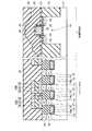
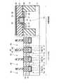
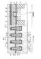
図1は、本発明の第1の実施形態に係る強誘電体記憶装置の斜視図を示す。ここでは、2セル分の概略的な構造を示しているが、セルアレイではこの2セル分の構造が繰り返されるものとする。 FIG. 1 is a perspective view of a ferroelectric memory device according to the first embodiment of the present invention. Although a schematic structure for two cells is shown here, the structure for two cells is repeated in the cell array.
図1に示すように、例えばP型の半導体基板(例えばシリコン基板)11内には、素子分離絶縁膜13からなる素子分離用溝が複数個形成され、ゲート溝14が複数個形成されている。ここで、素子分離用溝はX方向に延在し、ゲート溝14は素子分離溝を横切るようにY方向に延在する。尚、隣接セル間で導通しないようにするために、ゲート溝14は素子分離用溝よりも浅く形成することが望ましい。 As shown in FIG. 1, for example, in a P-type semiconductor substrate (for example, a silicon substrate) 11, a plurality of element isolation trenches made of an element
ゲート溝14の下部領域内にはゲート絶縁膜15を介してゲート電極16a,16b,16cが形成され、ゲート溝14の上部領域内には埋め込み絶縁膜17が形成されている。このようにして、トランジスタTra,Trb,Trcが半導体基板11内に埋め込まれている。尚、ゲート絶縁膜15は、ゲート電極16a,16b,16cとゲート溝14との間だけでなく、埋め込み絶縁膜17とゲート溝14との間にも存在してよい。
ゲート溝14及び素子分離用溝以外の半導体基板11の表面には例えばn−型の低濃度拡散層18が形成され、この低濃度拡散層18の表面には例えばn+型の高濃度拡散層23が形成されている。ここで、低濃度拡散層18は、ゲート電極16a,16b,16cの上面よりも深く形成することが望ましい。尚、低濃度及び高濃度拡散層18,23は、ゲート溝14と素子分離用溝とによって分離された素子領域に形成されるため、島状のピラー構造になっている。For example, an n− type low
ゲート電極16a,16c間の素子領域上には2次元強誘電体キャパシタ29aが形成され、ゲート電極16b,16c間の素子領域上には2次元強誘電体キャパシタ29bが形成されている。これらキャパシタ29a,29bは下部電極26と強誘電体膜27と上部電極28とでそれぞれ構成されており、これら下部電極26、強誘電体膜27及び上部電極28はセル毎に分離されている。尚、下部電極26の下に、TiAlN等からなるバリア膜(図示せず)を設けてもよい。また、キャパシタ29a,29b上には、コンタクト31b,31cを介して、Y方向に延在するプレート線32b,32cが形成されている。 A two-dimensional
ゲート電極16aを挟んでキャパシタ29aと反対側の素子領域上にはコンタクト31aが形成され、ゲート電極16bを挟んでキャパシタ29bと反対側の素子領域上にはコンタクト31dが形成されている。これらコンタクト31a,31d上にはプレート線32b,32cと同一レベルに配置された配線層32a,32dが形成されている。この配線層32a,32d上にはコンタクト34a,34bが形成され、このコンタクト34a,34d上にはX方向に延在するビット線35が形成されている。 A
このような第1の実施形態では、2つのセル間のトランジスタTrcをフィールドシールド領域として機能させるために、トランジスタTrcのソース/ドレイン間の電圧が0.5V〜4V程度の時、トランジスタTrcのゲート電極16cにはサブスレショルド電流が10−10A以下程度になるような電圧が印加されている。そして、このフィールドシールド領域を境界に、2つのセルが対称的な構造となるように配置されている。ここで、一方のセルはトランジスタTraとキャパシタ29aとで構成され、トランジスタTraにおけるゲート溝14の側面及び底面領域がチャネルとして機能し、このセルはコンタクト31a,34a及び配線層32aを介してビット線35につながっている。他方のセルはトランジスタTrbとキャパシタ29bとで構成され、トランジスタTrbにおけるゲート溝14の側面及び底面領域がチャネルとして機能し、このセルはコンタクト31d,34b及び配線層32dを介してビット線35につながっている。In such a first embodiment, in order for the transistor Trc between two cells to function as a field shield region, when the voltage between the source and drain of the transistor Trc is about 0.5 V to 4 V, the gate of the transistor Trc A voltage is applied to the
上記第1の実施形態によれば、メモリセル部のトランジスタTra,Trbを基板11内に埋め込み、ゲート溝14と素子分離用溝によって規定された島状のピラー領域を、キャパシタ29a,29bとソース/ドレインとの接続部として使う。これにより、キャパシタ29a,29bとソース/ドレインとを接続するコンタクトプラグや、キャパシタ29a,29bと基板11間の層間絶縁膜を無くすことができる。このため、第1の配線層32a,32b,32c,32dから基板11までの深さを従来の約半分にすることが可能となり、ビット線35に接続するコンタクトのアスペクト比を低減することができる。 According to the first embodiment, the transistors Tra and Trb of the memory cell portion are embedded in the
また、フィールドシールド領域として機能するゲート16cが埋め込まれた領域は、トランスファゲート16a,16bが埋め込まれた領域と同時に形成することができる上、合わせずれによるピラー領域の変動が無いので、フィールドシールド領域を容易に形成することができる。 The region embedded with the
[第2の実施形態]
第2の実施形態は、上記第1の実施形態の変形例であり、フィールドシールド領域として通常のSTI(Shallow Trench Isolation)構造の素子分離領域を採用したものである。[Second Embodiment]
The second embodiment is a modification of the first embodiment, in which an element isolation region having a normal STI (Shallow Trench Isolation) structure is employed as a field shield region.
図2は、本発明の第2の実施形態に係る強誘電体記憶装置の斜視図を示す。図2に示すように、第2の実施形態において、第1の実施形態と異なる点は、2つのセル間に素子分離用溝をY方向に形成し、この素子分離用溝を素子分離絶縁膜13で埋め込み、これをフィールドシールド領域として機能させている点である。このY方向に延在する素子分離用溝は、X方向に延在する素子分離用溝と同程度の深さで同時に形成すればよい。 FIG. 2 is a perspective view of a ferroelectric memory device according to the second embodiment of the present invention. As shown in FIG. 2, the second embodiment is different from the first embodiment in that an element isolation groove is formed in the Y direction between two cells, and the element isolation groove is formed as an element isolation insulating film. 13 is embedded, and this is functioned as a field shield region. The element isolation grooves extending in the Y direction may be formed simultaneously with the same depth as the element isolation grooves extending in the X direction.
上記第2の実施形態によれば、上記第1の実施形態と同様の効果を得ることができる。さらに、フィールドシールド領域として通常の素子分離領域を採用することで、第1の実施形態のようにフィールドシールド領域として機能させるためにトランジスタTrcを制御する必要がないため、安定したフィールドシールド領域を実現できる。 According to the second embodiment, the same effect as that of the first embodiment can be obtained. Further, by adopting a normal element isolation region as the field shield region, it is not necessary to control the transistor Trc in order to function as the field shield region as in the first embodiment, so a stable field shield region is realized. it can.
[第3の実施形態]
第3の実施形態は、上記第1の実施形態の変形例であり、TC並列ユニット直列接続型のセル構造を採用したものである。ここで、TC並列ユニット直列接続型のセル構造とは、メモリセルトランジスタ(T)のソース/ドレイン間にキャパシタ(C)の両端をそれぞれ接続し、これをユニットセルとし、このユニットセルを複数直列に接続したセル構造のことをいう。[Third Embodiment]
The third embodiment is a modification of the first embodiment and employs a TC parallel unit series connection type cell structure. Here, the TC parallel unit series connection type cell structure is such that both ends of the capacitor (C) are connected between the source / drain of the memory cell transistor (T), which is used as a unit cell, and a plurality of unit cells are connected in series. This refers to the cell structure connected to.
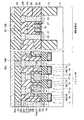
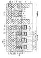
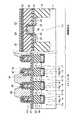
図3は、本発明の第3の実施形態に係る強誘電体記憶装置の斜視図を示す。尚、ここでは、4ビット単位のセル構造を示したが、8乃至16ビット単位等のセル構造に種々変更することは可能である。 FIG. 3 is a perspective view of a ferroelectric memory device according to the third embodiment of the present invention. Although a cell structure in units of 4 bits is shown here, various changes to cell structures in units of 8 to 16 bits are possible.
図3に示すように、第3の実施形態において、第1の実施形態と異なる点は、TC並列ユニット直列接続型のセル構造である点である。具体的には次のような構造になっている。 As shown in FIG. 3, the third embodiment is different from the first embodiment in that it has a TC parallel unit series connection type cell structure. Specifically, it has the following structure.
第1のセルは、トランジスタTraとキャパシタ29aとで構成されている。この第1のセルでは、トランジスタTraのソース/ドレインの一方には、キャパシタ29aの下部電極26が電気的に接続され、ソース/ドレインの他方には、コンタクト31c,31b及び配線32bを介してキャパシタ29aの上部電極28が電気的に接続されている。これにより、トランジスタTraのソース/ドレインとキャパシタ29aの上部電極28及び下部電極26とが並列に接続されている。 The first cell includes a transistor Tra and a
第2のセルは、トランジスタTrbとキャパシタ29bとで構成されている。この第2のセルでは、トランジスタTrbのソース/ドレインの一方には、キャパシタ29bの下部電極26が電気的に接続され、ソース/ドレインの他方には、コンタクト31c,31d及び配線32bを介してキャパシタ29bの上部電極28が電気的に接続されている。これにより、トランジスタTrbのソース/ドレインとキャパシタ29bの上部電極28及び下部電極26とが並列に接続されている。 The second cell includes a transistor Trb and a
第3のセルは、トランジスタTrcとキャパシタ29cとで構成されている。この第3のセルでは、トランジスタTrcのソース/ドレインの一方には、キャパシタ29cの下部電極26が電気的に接続され、ソース/ドレインの他方には、コンタクト31f,31e及び配線32cを介してキャパシタ29cの上部電極28が電気的に接続されている。これにより、トランジスタTrcのソース/ドレインとキャパシタ29cの上部電極28及び下部電極26とが並列に接続されている。 The third cell includes a transistor Trc and a
第4のセルは、トランジスタTrdとキャパシタ29dとで構成されている。この第4のセルでは、トランジスタTrdのソース/ドレインの一方には、キャパシタ29dの下部電極26が電気的に接続され、ソース/ドレインの他方には、コンタクト31f,31g及び配線32cを介してキャパシタ29dの上部電極28が電気的に接続されている。これにより、トランジスタTrdのソース/ドレインとキャパシタ29dの上部電極28及び下部電極26とが並列に接続されている。 The fourth cell includes a transistor Trd and a
そして、第1及び第2のセルにおいては、トランジスタTra,Trbと上部電極28との接続部分を共有することで、第1及び第2のセルが直列に接続されている。また、第3及び第4のセルにおいては、トランジスタTrc,Trdと上部電極28との接続部分を共有することで、第3及び第4のセルが直列に接続されている。また、第2及び第3のセルにおいては、トランジスタTrb,Trc間に設けられたトランジスタTrfのソース/ドレイン間の電圧が0.01V〜0.05V程度の時、トランジスタTrfのゲート電極16fに常にONとなるような電圧(10nA程度以上の電流が流れる電圧)を印加し、第2及び第3のセル間を導通させることで、第2及び第3のセルが直列に接続されている。 In the first and second cells, the first and second cells are connected in series by sharing a connection portion between the transistors Tra and Trb and the
また、トランジスタTraの左隣には、第1乃至第4のセルからなるブロックを選択するためのブロック選択トランジスタTreが配置されている。このトランジスタTreのソース/ドレインの一方は第1乃至第4のセルからなるブロックに接続され、ソース/ドレインの他方はコンタクト31a,34及び配線層32aを介してビット線35に接続されている。 Further, a block selection transistor Tre for selecting a block composed of the first to fourth cells is arranged on the left side of the transistor Tra. One of the source / drain of the transistor Tre is connected to a block made up of first to fourth cells, and the other of the source / drain is connected to a
上記第3の実施形態によれば、上記第1の実施形態と同様の効果を得ることができる。さらに、TC並列ユニット直列接続型構造にすることで、セル面積の縮小を図ることができる。 According to the third embodiment, the same effect as that of the first embodiment can be obtained. Furthermore, the cell area can be reduced by adopting the TC parallel unit series connection structure.
また、第2及び第3のセル間を導通させるために、常にオンとなる埋め込みトランジスタTrfを設けている。従って、キャパシタ29a,29b,29c,29dを加工する際、キャパシタ29a,29b,29c,29dの両端下には埋め込み絶縁膜17が存在するため、基板11がえぐれてしまうことを防止できる。 In addition, a buried transistor Trf that is always on is provided in order to make the second and third cells conductive. Therefore, when the
[第4の実施形態]
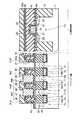
第4の実施形態は、第3の実施形態の変形例であり、第2及び第3のセル間を導通させるために、常にオンとなる埋め込みトランジスタを設けずに、第2の及び第3のセルキャパシタ下の拡散層を一続きに連続させたものである。[Fourth Embodiment]
The fourth embodiment is a modification of the third embodiment. In order to make the second and third cells conductive, the second and third transistors are not provided without providing an embedded transistor that is always turned on. The diffusion layer under the cell capacitor is continuously connected.
図4は、本発明の第4の実施形態に係る強誘電体記憶装置の斜視図を示す。図4に示すように、第4の実施形態において、第3の実施形態と異なる点は、キャパシタ29b、29c下の拡散層18,23を一続きに連続させて、第2及び第3のセル間を導通させることで、第2及び第3のセルを直列に接続している点である。 FIG. 4 is a perspective view of a ferroelectric memory device according to the fourth embodiment of the present invention. As shown in FIG. 4, the fourth embodiment differs from the third embodiment in that the diffusion layers 18 and 23 under the
上記第4の実施形態によれば、上記第3の実施形態と同様の効果を得ることができる。さらに、導通領域として通常の拡散領域を採用することで、第3の実施形態のように導通領域として機能させるためにトランジスタTrcを制御する必要がないため、安定した導通領域を実現できる。 According to the fourth embodiment, the same effects as in the third embodiment can be obtained. Furthermore, by adopting a normal diffusion region as the conduction region, it is not necessary to control the transistor Trc in order to function as a conduction region as in the third embodiment, so that a stable conduction region can be realized.
[第5の実施形態]
第5の実施形態は、メモリセル部と制御回路部とを示したものであり、メモリセル部は上記第1の実施形態の構造を適用し、制御回路部は通常の平面トランジスタを適用したものである。[Fifth Embodiment]
The fifth embodiment shows a memory cell unit and a control circuit unit. The memory cell unit applies the structure of the first embodiment, and the control circuit unit uses a normal planar transistor. It is.
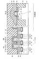
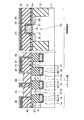
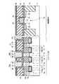
図5は、本発明の第5の実施形態に係る強誘電体記憶装置の断面図を示す。図5に示すように、制御回路部は、半導体基板11上にゲート絶縁膜19を介してゲート電極20が形成されている。このゲート電極20の側面にはスペーサ22が形成され、ゲート電極20の両側には拡散層21,23が形成されている。この拡散層21,23にはコンタクト31e,31fが接続され、このコンタクト31e,31fにはメモリセル部の配線層32a,32b,32c,32dと同一レベルに配置された配線層32e,32fが接続されている。また、メモリセル部のビット線35aと同一レベルに配線層35bが配置されている。尚、メモリセル部は第1の実施形態と同様の構造であるため説明は省略する。 FIG. 5 is a sectional view of a ferro-electric memory device according to the fifth embodiment of the present invention. As shown in FIG. 5, in the control circuit portion, a
このような構造では、メモリセル部における第1の配線層32a,32b,32c,32dから基板11までの深さを浅くすることができる。このため、基板11と第1の配線層32a,32dを接続するコンタクト31a,31dの高さ(第1の配線層下の層間絶縁膜の膜厚)をX1、2次元キャパシタ29a,29bの膜厚をY1、制御回路におけるゲート電極20の高さをZ1とした場合、次の式(1),(2)の関係が成り立つ。尚、キャパシタ29a,29bの膜厚Y1は、下部電極26の下界面から強誘電体膜27に接している上部電極28の1層目の膜の上界面までの膜厚とする。 With such a structure, the depth from the
X1≦2.5Y1…(1)
X1≦6Z1…(2)
図6乃至図15は、本発明の第5の実施形態に係る強誘電体記憶装置の製造工程の断面図を示す。以下に、第5の実施形態に係る強誘電体記憶装置の製造方法について説明する。X1 ≦ 2.5Y1 (1)
X1 ≦ 6Z1 (2)
6 to 15 are sectional views showing the steps of manufacturing a ferroelectric memory device according to the fifth embodiment of the present invention. The method for manufacturing the ferroelectric memory device according to the fifth embodiment will be described below.
まず、図6に示すように、例えばP型の半導体基板(例えばシリコン基板)11上に、例えばSiN等からなるストッパー絶縁膜12が堆積される。次に、半導体基板11内に素子分離溝が形成され、この素子分離用溝内に例えばTEOS(Tetra Ethyl Ortho Silicate)等の素子分離絶縁膜13が埋め込まれる。その後、ストッパー絶縁膜12の上面が露出するまで、素子分離絶縁膜13がCMP(Chemical Mechanical Polish)で平坦化される。これにより、半導体基板11内にSTI構造の素子分離領域が形成される。尚、図6の断面図には示されていないが、メモリセル部においても素子分離領域は形成されている。 First, as shown in FIG. 6, a
次に、図7に示すように、メモリセル部において、半導体基板11内に埋め込みトランジスタ用のゲート溝14が形成される。次に、ゲート溝14内の底面及び側面にゲート酸化膜15が形成され、その後、例えば多結晶シリコン等の導電性のゲート電極材がゲート溝14内に堆積される。次に、ストッパー絶縁膜12の上面が露出するまで、ゲート電極材がCMPで平坦化される。次に、RIE(Reactive Ion Etching)のような異方性エッチング又はCDE(Chemical Dry Etching)のような等方性エッチングにより、ゲート電極材及びゲート酸化膜15がゲート溝14内にリセスされる。これにより、半導体基板11の上面より低い位置に上面が位置するゲート電極16a,16b,16cが形成される。次に、ゲート溝14内に例えばTEOS膜等からなる埋め込み絶縁膜17が堆積され、この埋め込み絶縁膜17がCMPで平坦化され、ストッパー絶縁膜12の上面が露出される。その後、燐酸処理やCDE法で、ストッパー絶縁膜12が除去される。 Next, as shown in FIG. 7, a
次に、図8に示すように、半導体基板11の表面にダミーゲート絶縁膜(図示せず)が形成された後、メモリセル部における素子領域にn−型の低濃度拡散層18が形成される。次に、ダミーゲート絶縁膜を除去した後、半導体基板11の表面にゲート酸化膜19が形成される。次に、例えば多結晶シリコン等からなるゲート電極材が堆積され、このゲート電極材がリソグラフィ法でパターンニングされることで、制御回路部にゲート電極20が形成される。Next, as shown in FIG. 8, after a dummy gate insulating film (not shown) is formed on the surface of the
次に、図9に示すように、制御回路部において、半導体基板11の表面にn−型の低濃度拡散層21が形成された後、ゲート電極20の側面にスペーサ22が形成される。次に、制御回路部及びメモリセル部の両方において、半導体基板11の表面にn+型の高濃度拡散層23が形成される。これにより、トランジスタTra,Trb,Trc,Trdが形成される。その後、メモリセル部及び制御回路部に、例えばSiN膜、アルミナ、チタニア等からなる層間膜24が堆積され、この層間膜24上に例えばTEOS、BPSG(Boron Phosphorous Silicate Glass)、SOG(Spin On Glass)等からなる層間膜25が堆積される。Next, as shown in FIG. 9, after the n− -type low
尚、層間膜24を堆積する前に、メモリセル部及び制御回路部の拡散層23や制御回路部のゲート電極20上に、例えばNi、Ti、Co等からなる金属シリサイド膜を自己整合的に形成してもよい。この場合、メモリセル部の拡散層23上の金属シリサイド膜と制御回路部の拡散層23上の金属シリサイド膜とは、同一の材料及び同一の膜厚で形成される。このようなシリサイド膜により、低抵抗化を実現できるだけでなく、メモリセル部においては、キャパシタの下部電極材料にシリコンが拡散するのを抑制し、コンタクトを良好にするという効果も得られる。 Before depositing the
次に、図10に示すように、メモリセル部のみ、層間膜25が除去される。ここで、制御回路部に残された層間膜25の端部は、できるだけ緩やかなテーパー形状をしている方が望ましいので、層間膜25は、RIEのような異方性エッチングを用いて除去するよりも、HF、NH4F等によるウエットエッチングやCDEのような等方性エッチングを用いて除去することが望ましい。Next, as shown in FIG. 10, the
次に、図11に示すように、メモリセル部のみ層間膜24が除去され、メモリセル部のゲート酸化膜19及び埋め込み絶縁膜17の上面が露出される。ここで、層間膜24は、RIEのような異方性エッチングを用いて除去してもよいが、燐酸やCDE法を用いて除去する方が望ましい。 Next, as shown in FIG. 11, the
次に、図12に示すように、酸化膜系の薄い絶縁膜(図示せず)が堆積され、キャパシタが搭載される位置のゲート酸化膜19が露出するように、絶縁膜がリソグラフィでパターニングされる。そして、このパターニングされた絶縁膜をマスクとして、キャパシタが搭載される位置のゲート酸化膜19が除去される。尚、ゲート酸化膜19は、必ずしも部分的に除去する必要はなく、メモリセル部の全部を除去してもよい。 Next, as shown in FIG. 12, an oxide-based thin insulating film (not shown) is deposited, and the insulating film is patterned by lithography so that the
次に、スパッタ、塗布法、MOCVD(Metal Organic Chemical Vapor Deposition)法により、下部電極26、強誘電体膜27、上部電極28が順に形成される。ここで、下部電極26としては、例えば、Ir、IrO2や、IrとPtとの積層膜、IrO2とPtとの積層膜等があげられる。強誘電体膜27としては、例えば、PZT、SBT、BLT膜などがあげられる。上部電極28としては、例えば、Pt、IrO2、SrRuOや、これらPt、IrO2、SrRuOの積層膜があげられる。尚、下部電極26としてIrを含む材料を用いた場合は、下部電極26の下に例えばTiN,TiAlN等からなる酸素バリア膜を設ける方が望ましい。Next, the
次に、図13に示すように、リソグラフィ及びRIEにより下部電極26、強誘電体膜27及び上部電極28がパターニングされ、メモリセル部に強誘電体キャパシタ29a,29bが形成される。この際、パターニング時のマスク材としては、レジストを用いてもよいが、高温処理を考慮すると、酸化系の膜(アルミナ)、TiN膜、TiAlN膜等を用いるのが望ましい。尚、キャパシタ29a,29bの上面と層間膜25の上面とがほぼ等しい高さ(±1500Å程度)になるように調整しておくことが望ましい。 Next, as shown in FIG. 13, the
次に、図14に示すように、例えばTEOSやSOG等の層間絶縁膜30が堆積され、この層間絶縁膜30がCMPで平坦化される。 Next, as shown in FIG. 14, an
次に、図15に示すように、上部電極28に接続するコンタクト31b,31cが形成され、拡散層23に接続するコンタクト31a,31d,31e,31fが形成され、コンタクト31a,31b,31c,31d,31e,31fに接続する第1の配線層32a,32b,32c,32d,32e,32fが形成される。ここで、キャパシタ29a,29bに接続する第1の配線層32b,32cは、プレート線として機能する。 Next, as shown in FIG. 15,
次に、図5に示すように、層間絶縁膜30上に層間絶縁膜33が形成される。次に、この層間絶縁膜33内に、コンタクト34a,34b及び第2の配線層35a,35bが形成される。ここで、メモリセル部における第2の配線層35aは、ビット線として機能する。尚、その後、第3、第4の配線層を形成してもよく、各種配線はAlやCuのどちらでもよい。 Next, as shown in FIG. 5, an
上記第5の実施形態によれば、上記第1の実施形態における効果が得られるだけでなく、さらに次のような効果も得ることができる。 According to the fifth embodiment, not only the effects of the first embodiment but also the following effects can be obtained.
第5の実施形態では、メモリセル部は埋め込みトランジスタTra,Trbを形成し、制御回路部は通常の平面トランジスタTrdを形成している。これにより、高い信頼性や電流駆動能力を要求される制御回路部は従来と何ら変わるところ無く十分な信頼性等を確保することができる。 In the fifth embodiment, the memory cell portion forms buried transistors Tra and Trb, and the control circuit portion forms a normal planar transistor Trd. As a result, the control circuit unit that requires high reliability and current drive capability can ensure sufficient reliability without any difference from the conventional one.
また、メモリセル部のゲート電極16a,16bを基板11内に埋め込み、キャパシタ29a,29bと基板11間の層間膜をなくすことで、メモリセル部のキャパシタ29a,29bによる段差と制御回路部のゲート電極20による段差とをほぼ同じにすることができる。このため、制御回路部にダミーパターンを設けなくても、メモリセル部におけるキャパシタ29a,29b上の層間絶縁膜30の平坦化工程と、制御回路部におけるゲート電極20上の層間絶縁膜30の平坦化工程とを同時に容易に行うことができる。 Further, by embedding the
また、図10の工程において、メモリセル部の層間膜25を等方性エッチングで除去することで、制御回路部に残された層間膜25の端部をなだらかなテーパー形状にすることができる。このように、層間膜25の端部をなだらかなテーパー形状にすることで、図13のキャパシタの加工時、オーバーエッチング量を抑制することができ、キャパシタの加工が容易になる。 In the step of FIG. 10, the
また、キャパシタ29a,29bの上面と層間膜25の上面とがほぼ等しい高さにすることで、その後、層間絶縁膜30を研磨する際に、メモリセル部と制御回路部のどちらも同じ高さの突起が同様の密度で存在するため、研磨後の平坦性が良好となる。 In addition, since the upper surfaces of the
尚、メモリセル部は、上記第1の実施形態の構造に限定されず、その他の実施形態の構造を適用することも勿論可能である。 Note that the memory cell portion is not limited to the structure of the first embodiment, and it is of course possible to apply the structures of other embodiments.
[第6の実施形態]
第6の実施形態は、上記第5実施形態の2次元キャパシタを3次元キャパシタに変形した例である。[Sixth Embodiment]
The sixth embodiment is an example in which the two-dimensional capacitor of the fifth embodiment is modified to a three-dimensional capacitor.
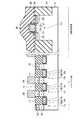
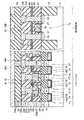
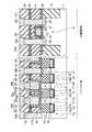
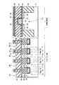
図16は、本発明の第6の実施形態に係る強誘電体記憶装置の断面図を示す。図16に示すように、第6の実施形態において、上記第5の実施形態と異なる点は、強誘電体キャパシタ29a,29bが3次元キャパシタ構造になっている点である。つまり、下部電極26の上面及び側面に強誘電体膜27が形成され、この強誘電体膜27の上面及び側面に上部電極28が形成されることで、強誘電体膜27及び上部電極28がXYZ方向に延在している。 FIG. 16 is a sectional view of a ferro-electric memory device according to the sixth embodiment of the present invention. As shown in FIG. 16, the sixth embodiment is different from the fifth embodiment in that the
このような構造では、メモリセル部における第1の配線層32a,32b,32c,32dから基板11までの深さを浅くすることができる。このため、基板11と第1の配線層32a,32dを接続するコンタクト31a,31dの高さ(第1の配線層下の層間絶縁膜の膜厚)をX2、3次元キャパシタ29a,29bの膜厚をY2、制御回路におけるゲート電極20の高さをZ2とした場合、次の式(3),(4)の関係が成り立つ。 With such a structure, the depth from the
X2≦1.6Y2…(3)
X2≦9Z2…(4)
図17乃至図22は、本発明の第6の実施形態に係る強誘電体記憶装置の製造工程の断面図を示す。以下に、第6の実施形態に係る強誘電体記憶装置の製造方法について説明する。X2 ≦ 1.6Y2 (3)
X2 ≦ 9Z2 (4)
FIGS. 17 to 22 are sectional views showing the steps of manufacturing a ferroelectric memory device according to the sixth embodiment of the present invention. The method for manufacturing the ferroelectric memory device according to the sixth embodiment will be described below.
まず、図6乃至図11に示すように、第5の実施形態同様、メモリセル部のみ、層間膜24,25が除去される。その後、キャパシタが搭載される位置のゲート酸化膜19が除去される。尚、ゲート酸化膜19は、必ずしも部分的に除去する必要はなく、メモリセル部の全部を除去してもよい。 First, as shown in FIGS. 6 to 11, the
次に、図17に示すように、メモリセル部及び制御回路部に、下部電極26が形成される。ここで、下部電極26の材料としては、Ir、IrO2や、IrとPtとの積層膜、IrO2とPtとの積層膜等があげられる。尚、下部電極26の下にTiN,TiAlN等からなる酸素バリア膜を設けてもよい。Next, as shown in FIG. 17, the
次に、図18に示すように、下部電極26上に例えば酸化膜,TiN膜,TiAlN膜等からなるマスク材(図示せず)が形成されてパターニングされる。このパターニングされたマスク材を用いて、下部電極26がRIEで加工される。これにより、メモリセル部に、通常よりも厚い下部電極26が形成される。その後、マスク材は除去される。尚、下部電極26の下に酸素バリア膜を設けた場合は、バリア膜の上面で下部電極26のエッチングを一旦ストップさせた後、酸素バリア膜をRIEでエッチングすることが望ましい。 Next, as shown in FIG. 18, a mask material (not shown) made of, for example, an oxide film, a TiN film, a TiAlN film or the like is formed on the
次に、図19に示すように、拡散バリア膜(図示せず),強誘電体膜27,上部電極28が順に堆積される。ここで、拡散バリア膜としては、TiAlN、Ir、IrO2、SrRuOなどがあげられる。強誘電体膜27としては、PZT、SBT、BLT膜などがあげられる。上部電極28としては、Pt、IrO2、SrRuOや、これらPt、IrO2、SrRuOの積層膜があげられる。尚、拡散バリア膜は、必須ではないが、特にPZTで強誘電体膜27が形成されている場合は、この強誘電体膜27のPbが下部電極26へ拡散することを防ぐために、設ける方が望ましい。Next, as shown in FIG. 19, a diffusion barrier film (not shown), a
次に、図20に示すように、上部電極28上に例えば酸化膜,TiN膜,TiAlN膜等からなるマスク材(図示せず)が形成されてパターニングされる。このパターニングされたマスク材を用いて、拡散バリア膜(図示せず),強誘電体膜27,上部電極28がRIEで加工される。これにより、メモリセル部に3次元強誘電体キャパシタ29a,29bが形成される。その後、マスク材は除去される。 Next, as shown in FIG. 20, a mask material (not shown) made of, for example, an oxide film, a TiN film, a TiAlN film or the like is formed on the
次に、図21に示すように、例えばTEOSやSOG等の層間絶縁膜30が堆積され、この層間絶縁膜30がCMPで平坦化される。 Next, as shown in FIG. 21, an
次に、図22に示すように、上部電極28に接続するコンタクト31b,31cが形成され、拡散層23に接続するコンタクト31a,31d,31e,31fが形成され、コンタクト31a,31b,31c,31d,31e,31fに接続する第1の配線層32a,32b,32c,32d,32e,32fが形成される。 Next, as shown in FIG. 22,
次に、図16に示すように、層間絶縁膜30上に層間絶縁膜33が形成される。次に、この層間絶縁膜33内に、コンタクト34a,34b及び第2の配線層35a,35bが形成される。 Next, as shown in FIG. 16, an
上記第6の実施形態によれば、上記第5の実施形態と同様の効果を得ることができる。さらに、3次元キャパシタを用いることで、キャパシタ容量を増大できるという効果も得られる。 According to the sixth embodiment, the same effect as in the fifth embodiment can be obtained. Further, the use of a three-dimensional capacitor can also provide an effect that the capacitor capacity can be increased.
[第7の実施形態]
第7の実施形態は、上記第6の実施形態における3次元キャパシタの形状を変形させたものである。[Seventh Embodiment]
In the seventh embodiment, the shape of the three-dimensional capacitor in the sixth embodiment is modified.
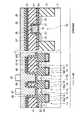
図23は、本発明の第7の実施形態に係る強誘電体記憶装置の断面図を示す。図23に示すように、第7の実施形態において、上記第6の実施形態と異なる点は、3次元キャパシタ29a,29bの形状である。つまり、第6の実施形態では、強誘電体膜27及び上部電極28をXYZ方向に延在させているのに対し、第7の実施形態では、下部電極26及び強誘電体膜27をXYZ方向に延在させている。 FIG. 23 is a sectional view of a ferro-electric memory device according to the seventh embodiment of the present invention. As shown in FIG. 23, the seventh embodiment differs from the sixth embodiment in the shapes of the three-
尚、第7の実施形態においても、第6の実施形態と同様に、上記式(3),(4)の関係を満たした構造になっている。 In the seventh embodiment, as in the sixth embodiment, the structure satisfies the relationships of the above formulas (3) and (4).
図24乃至図33は、本発明の第7の実施形態の第1の製造方法による製造工程の断面図を示す。以下に、第7の実施形態に係る強誘電体記憶装置の第1の製造方法について説明する。 24 to 33 are sectional views showing manufacturing steps according to the first manufacturing method of the seventh embodiment of the present invention. The first manufacturing method of the ferroelectric memory device according to the seventh embodiment will be explained below.
まず、図6乃至図8に示すように、第5の実施形態同様、メモリセル部に埋め込みゲート電極14が形成された後、制御回路部にゲート電極20が形成される。 First, as shown in FIGS. 6 to 8, after the embedded
次に、図24に示すように、制御回路部において、半導体基板11の表面にn−型の低濃度拡散層21が形成された後、ゲート電極20の側面にゲートスペーサー22が形成される。次に、制御回路部及びメモリセル部の両方において、n+型の高濃度拡散層23が形成される。これにより、トランジスタTra,Trb,Trc,Trdが形成される。次に、メモリセル部及び制御回路部に例えばSiN膜、アルミナ、チタニア等からなる層間膜24が形成され、この層間膜24上に例えばBPSG、TEOS、SOG等からなる絶縁膜40が形成される。Next, as shown in FIG. 24, after the n− -type low
次に、図25に示すように、絶縁膜40がパターニングされ、メモリセル部に所定の密度で絶縁膜40からなるダミーパターンが形成される。ここで、メモリセル部のダミーパターンの高さと制御回路部のゲート電極20の高さ(厳密には層間膜24の上面の高さ)とをほぼ等しくするために、絶縁膜40の堆積膜厚を調整することが望ましい。尚、このダミーパターンは、必ずしも設ける必要はないが、後のCMP時におけるメモリセル部のディッシングを防止するためには、設ける方が望ましい。但し、以下の工程においては、ダミーパターンの図示は省略する。 Next, as shown in FIG. 25, the insulating
次に、図26に示すように、層間膜24上に例えばBPSG、TEOS、SOG等からなる層間膜41が形成され、この層間膜41上に例えばアルミナ等からなる拡散防止膜42が形成される。この拡散防止膜42は、強誘電体膜27を構成するPZTやSBTの不純物が、強誘電体膜27から基板11に拡散することを防止する膜であり、特に、PZTの場合のPbが拡散することを防止するものである。 Next, as shown in FIG. 26, an
次に、図27に示すように、層間膜24,41及び拡散防止膜42がRIEで選択的に除去され、キャパシタ溝43が形成される。この際、層間膜24の上面で一旦エッチングをストップした後、層間膜24をエッチングすることが望ましい。次に、キャパシタが搭載される位置のゲート酸化膜19が除去される。 Next, as shown in FIG. 27, the
次に、図28に示すように、キャパシタ溝43内及び拡散防止膜42上に、下部電極26が形成される。この下部電極26としては、例えば、Ir、IrO2や、IrとPtとの積層膜、IrO2とPtとの積層膜等があげられる。尚、下部電極26の下にTiN,TiAlN等からなる酸素バリア膜を設ける方が望ましい。Next, as shown in FIG. 28, the
次に、図29に示すように、下部電極26上に埋め込み材44が形成される。この埋め込み材44としては、例えば、レジスト、SOG、P(リン)やB(ボロン)がドープされたSOG、TEOS、P(リン)やB(ボロン)がドープされたTEOS等があげられる。次に、拡散防止膜42上の下部電極26が露出するまで、埋め込み材44がCMPで平坦化される。ここで、埋め込み材44がSOGやレジストで形成された場合は、このCMPの工程は省略することが可能である。次に、キャパシタ溝43内の埋め込み材44の上部がRIEで除去される。 Next, as shown in FIG. 29, a filling
次に、図30に示すように、下部電極26がエッチバックされる。これにより、メモリセル部では、キャパシタ溝43毎(セル毎)に下部電極26が分断され、制御回路部では、下部電極26は全て除去される。この際、拡散防止膜42が残るようにエッチバックを制御することが望ましい。また、キャパシタ溝43内の下部電極26上には埋め込み材44が存在するため、埋め込み材44の上部が除去されるだけで、キャパシタ溝43内の下部電極26が除去されることを防ぐことができる。 Next, as shown in FIG. 30, the
次に、図31に示すように、例えばMOCVD法を用いて、強誘電体膜27、上部電極28が順に堆積される。強誘電体膜27としては、例えば、PZT、SBT、BLT膜などがあげられる。上部電極28としては、例えば、Pt、IrO2、SrRuOや、これらPt、IrO2、SrRuOの積層膜があげられる。Next, as shown in FIG. 31, the
次に、図32に示すように、強誘電体膜27が露出するまで上部電極28がエッチバックで除去された後、拡散防止膜42が露出するまで強誘電体膜27がエッチバックで除去される。これにより、キャパシタ溝43内に強誘電体キャパシタ29a,29bが形成される。 Next, as shown in FIG. 32, after the
次に、図33に示すように、例えばTEOSやSOG等の層間絶縁膜30が堆積され、この層間絶縁膜30がCMPで平坦化される。次に、上部電極28に接続するコンタクト31b,31cが形成され、拡散層23に接続するコンタクト31a,31d,31e,31fが形成され、コンタクト31a,31b,31c,31d,31e,31fに接続する第1の配線層32a,32b,32c,32d,32e,32fが形成される。 Next, as shown in FIG. 33, for example, an
次に、図23に示すように、層間絶縁膜30上に層間絶縁膜33が形成される。次に、この層間絶縁膜33内に、コンタクト34a,34b及び第2の配線層35a,35bが形成される。 Next, as shown in FIG. 23, an
図34乃至図38は、本発明の第7の実施形態の第2の製造方法による製造工程の断面図を示す。以下に、第7の実施形態に係る強誘電体記憶装置の第2の製造方法について説明する。 34 to 38 are sectional views showing manufacturing steps according to the second manufacturing method of the seventh embodiment of the present invention. The second manufacturing method of the ferroelectric memory device according to the seventh embodiment will be described below.
まず、図6乃至図8、図24乃至図30の工程を経た後、図34に示すように、例えばMOCVD法を用いて、強誘電体膜27、上部電極28が順に堆積される。強誘電体膜27としては、例えば、PZT、SBT、BLT膜などがあげられる。上部電極28としては、例えば、Pt、IrO2、SrRuOや、これらPt、IrO2、SrRuOの積層膜があげられる。First, after the steps of FIGS. 6 to 8 and FIGS. 24 to 30, as shown in FIG. 34, a
次に、図35に示すように、上部電極28上に例えば酸化膜,TiN膜,TiAlN膜等からなるマスク材45が形成されてパターニングされる。 Next, as shown in FIG. 35, a
次に、図36に示すように、上部電極28及び強誘電体膜27がRIEでエッチングされ、上部電極28及び強誘電体膜27がキャパシタ溝43毎に分断される。この際、マスク材45を用いて上部電極28が確実に残るようにエッチングする。そして、このエッチング時の条件としては、マスク材45が無くなり、上部電極28の高さを減らす程度が望ましい。 Next, as shown in FIG. 36, the
尚、図34の工程を下部電極26のリセス処理なしで行うことも可能であり、この場合は、図36の工程時に、下部電極26を上部電極28及び強誘電体膜27と同時に除去すればよい。 It is possible to perform the process of FIG. 34 without recessing the
次に、図37に示すように、上部電極28の上部がRIEで除去される。ここで、上部電極28による段差は、500Å程度に低減することが望ましい。このようにして、キャパシタ溝43内に強誘電体キャパシタ29a,29bが形成される。 Next, as shown in FIG. 37, the upper part of the
次に、図38に示すように、例えばTEOSやSOG等の層間絶縁膜30が堆積され、この層間絶縁膜30がCMPで平坦化される。次に、上部電極28に接続するコンタクト31b,31cが形成され、拡散層23に接続するコンタクト31a,31d,31e,31fが形成され、コンタクト31a,31b,31c,31d,31e,31fに接続する第1の配線層32a,32b,32c,32d,32e,32fが形成される。 Next, as shown in FIG. 38, for example, an
次に、図23に示すように、層間絶縁膜30上に層間絶縁膜33が形成される。次に、この層間絶縁膜33内に、コンタクト34a,34b及び第2の配線層35a,35bが形成される。 Next, as shown in FIG. 23, an
尚、上記第1及び第2の製造方法の説明中に用いた図において、キャパシタ29a,29bの上面部分の構造が図23のその部分の構造と多少異なっているが、理想的には図23のような構造になるようにプロセスを調整することが望ましい。 In the drawings used during the description of the first and second manufacturing methods, the structures of the upper surface portions of the
上記第7の実施形態によれば、上記第5の実施形態と同様の効果を得ることができる。さらに、3次元キャパシタを用いることで、キャパシタ容量を増大できるという効果も得られる。 According to the seventh embodiment, the same effect as in the fifth embodiment can be obtained. Further, the use of a three-dimensional capacitor can also provide an effect that the capacitor capacity can be increased.
[第8の実施形態]
第8の実施形態は、上記第6の実施形態において、ビット線とトランジスタとの接続構造を変形させたものである。[Eighth Embodiment]
In the eighth embodiment, the connection structure between the bit line and the transistor is modified in the sixth embodiment.
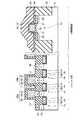
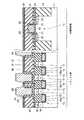
図39は、本発明の第8の実施形態に係る強誘電体記憶装置の断面図を示す。図39に示すように、第8の実施形態において、上記図16の第6の実施形態と異なる点は、ビット線35aとトランジスタTra,Trbのソース/ドレインとを、キャパシタ29c,29dの下部電極26を介して接続している点である。具体的には次のような構造になっている。 FIG. 39 is a sectional view of a ferro-electric memory device according to the eighth embodiment of the present invention. As shown in FIG. 39, the eighth embodiment differs from the sixth embodiment of FIG. 16 in that the
トランジスタTraの両側に位置する拡散層23上には、セルキャパシタ29aと、このセルキャパシタ29aと同構造のコンタクト用のキャパシタ29cとが配置されている。同様に、トランジスタTrbの両側に位置する拡散層23上には、セルキャパシタ29bと、このセルキャパシタ29bと同構造のコンタクト用のキャパシタ29dとが配置されている。そして、コンタクト用のキャパシタ29c,29dの下部電極26に、上部電極28及び強誘電体膜27を貫通するコンタクト31a,31dが接続されている。このようにして、トランジスタTra,Trbのソース/ドレインは、キャパシタ29c,29dの下部電極26、コンタクト31a,31d,34a,34b及び配線32a,32dを介して、ビット線35aに接続されている。 On the
尚、第8の実施形態においても、上記式(3),(4)の関係を満たした構造になっている。 In the eighth embodiment, the structure satisfies the relationships of the above formulas (3) and (4).
図40乃至図46は、本発明の第8の実施形態に係る強誘電体記憶装置の製造工程の断面図を示す。以下に、第8の実施形態に係る強誘電体記憶装置の製造方法について説明する。 40 to 46 are sectional views showing steps in manufacturing the ferro-electric memory device according to the eighth embodiment of the present invention. The method for manufacturing the ferroelectric memory device according to the eighth embodiment will be explained below.
まず、図6乃至図11に示すように、第5の実施形態同様、メモリセル部のみ、層間膜24,25が除去される。その後、キャパシタが搭載される位置のゲート酸化膜19が除去される。尚、ゲート酸化膜19は、必ずしも部分的に除去する必要はなく、メモリセル部の全部を除去してもよい。 First, as shown in FIGS. 6 to 11, the
次に、図40に示すように、メモリセル部及び制御回路部に、下部電極26が形成される。ここで、下部電極26の材料としては、Ir、IrO2や、IrとPtとの積層膜、IrO2とPtとの積層膜等があげられる。尚、下部電極26の下にTiN,TiAlN等からなる酸素バリア膜を設けてもよい。Next, as shown in FIG. 40, the
次に、図41に示すように、下部電極26上に例えば酸化膜,TiN膜,TiAlN膜等からなるマスク材(図示せず)が形成されてパターニングされる。このパターニングされたマスク材を用いて、下部電極26がRIEで加工される。これにより、メモリセル部に、通常よりも厚い下部電極26が形成される。その後、マスク材は除去される。尚、下部電極26の下に酸素バリア膜を設けた場合は、バリア膜の上面で下部電極26のエッチングを一旦ストップさせた後、酸素バリア膜をRIEでエッチングすることが望ましい。 Next, as shown in FIG. 41, a mask material (not shown) made of an oxide film, a TiN film, a TiAlN film or the like is formed on the
次に、図42に示すように、拡散バリア膜(図示せず),強誘電体膜27,上部電極28が順に堆積される。ここで、拡散バリア膜としては、TiAlN、Ir、IrO2、SrRuOなどがあげられる。強誘電体膜27としては、PZT、SBT、BLT膜などがあげられる。上部電極28としては、Pt、IrO2、SrRuOや、これらPt、IrO2、SrRuOの積層膜があげられる。尚、拡散バリア膜は、必須ではないが、特にPZTで強誘電体膜27が形成されている場合は、この強誘電体膜27のPbが下部電極26へ拡散することを防ぐために、設ける方が望ましい。Next, as shown in FIG. 42, a diffusion barrier film (not shown), a
次に、上部電極28上に例えば酸化膜,TiN膜,TiAlN膜等からなるマスク材(図示せず)が形成されてパターニングされる。このパターニングされたマスク材を用いて、拡散バリア膜(図示せず),強誘電体膜27,上部電極28がRIEで加工される。これにより、メモリセル部に3次元強誘電体キャパシタ29a,29b,29c,29dが形成される。その後、マスク材は除去される。 Next, a mask material (not shown) made of, for example, an oxide film, a TiN film, a TiAlN film or the like is formed on the
次に、図43に示すように、例えばTEOSやSOG等の層間絶縁膜30aが堆積され、この層間絶縁膜30aがCMPで平坦化される。次に、メモリセル部において、上部電極28を露出するコンタクトホール31b’,31c’が形成される。 Next, as shown in FIG. 43, an
次に、図44に示すように、メモリセル部において、下部電極26を露出するコンタクトホール31a’,31d’が形成される。 Next, as shown in FIG. 44,
次に、図45に示すように、制御回路部において、コンタクトホール32e’,32f’が形成される。次に、コンタクトホール31a’,31b’,31c’,31d’内に金属材が埋め込まれ、この金属材の上面が平坦化される。これにより、上部電極28に接続するコンタクト31b,31cが形成される。ここで、メモリセル部のコンタクト31a,31b,31c,31dは、AlやWで形成することが望ましく、この場合、AlやWの下部にTiNやTiAlN等の水素バリア膜を設ける方が望ましい。次に、コンタクトホール31e’,31f’内に金属材が埋め込まれ、この金属材の上面が平坦化される。これにより、拡散層23に接続するコンタクト31e,31fが形成される。 Next, as shown in FIG. 45,
次に、図46に示すように、コンタクト31a,31b,31c,31d,31e,31fに接続する第1の配線層32a,32b,32c,32d,32e,32fが形成される。 Next, as shown in FIG. 46,
次に、図39に示すように、第1の配線層32a,32b,32c,32d,32e,32fの周囲に層間絶縁膜30bが埋め込まれる。次に、第1の配線層32a,32b,32c,32d,32e,32f及び層間絶縁膜30b上に層間絶縁膜33が形成される。次に、この層間絶縁膜33内に、コンタクト34a,34b及び第2の配線層35a,35bが形成される。 Next, as shown in FIG. 39, an
上記第8の実施形態によれば、上記第6の実施形態と同様の効果を得ることができるだけでなく、さらに、ビット線35aとトランジスタTra,Trbのソース/ドレインとを接続するためのキャパシタ29c,29dを設けることで、次のような効果も得ることができる。 According to the eighth embodiment, not only the same effects as in the sixth embodiment can be obtained, but also the
下部電極26を加工する際、基板11が露出しないため、オーバーエッチングによって基板11がえぐれてしまうことを防止できる。また、キャパシタ29a,29bのコンタクトホールの31b’,31c’を形成する際、キャパシタ29a,29bはRIEによるダメージを受けるが、このダメージを回復する酸素雰囲気の回復アニールを行うことが可能となるため、より信頼性の高いキャパシタ29a,29bを形成できる。 Since the
尚、第8の実施形態において、3次元キャパシタの代わりに、2次元キャパシタを用いることも可能である。 In the eighth embodiment, a two-dimensional capacitor can be used instead of the three-dimensional capacitor.
[第9の実施形態]
第9の実施形態は、上記第7の実施形態において、ビット線とトランジスタとの接続構造を変形させたものである。[Ninth Embodiment]
In the ninth embodiment, the connection structure between the bit line and the transistor is modified in the seventh embodiment.
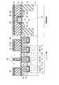
(第1の構造)
図47は、本発明の第9の実施形態に係る強誘電体記憶装置の第1の構造の断面図を示す。図47に示すように、第9の実施形態の第1の構造において、上記図23の第7の実施形態と異なる点は、ビット線35aとトランジスタTra,Trbのソース/ドレインとを、キャパシタ29c,29dの下部電極26を介して接続している点である。具体的には次のような構造になっている。(First structure)
FIG. 47 is a sectional view showing a first structure of the ferroelectric memory device according to the ninth embodiment of the present invention. As shown in FIG. 47, the first structure of the ninth embodiment differs from the seventh embodiment of FIG. 23 in that the
トランジスタTraの両側に位置する拡散層23上には、セルキャパシタ29aと、このセルキャパシタ29aと同構造のコンタクト用のキャパシタ29cとが配置されている。同様に、トランジスタTrbの両側に位置する拡散層23上には、セルキャパシタ29bと、このセルキャパシタ29bと同構造のコンタクト用のキャパシタ29dとが配置されている。そして、コンタクト用のキャパシタ29c,29dの下部電極26に、上部電極28及び強誘電体膜27を貫通するコンタクト31a,31dが接続されている。このようにして、トランジスタTra,Trbソース/ドレインは、キャパシタ29c,29dの下部電極26、コンタクト31a,31d,34a,34b及び配線32a,32dを介して、ビット線35aに接続されている。 On the
尚、第9の実施形態の第1の構造においても、上記式(3),(4)の関係を満たした構造になっている。 Note that the first structure of the ninth embodiment also has a structure that satisfies the relationships of the above expressions (3) and (4).
図48乃至図57は、本発明の第9の実施形態の第1の構造による製造工程の断面図を示す。以下に、第9の実施形態の第1の構造の製造方法について説明する。 48 to 57 are sectional views showing a manufacturing process according to the first structure of the ninth embodiment of the present invention. The method for manufacturing the first structure of the ninth embodiment will be described below.
まず、図6乃至図8に示すように、第5の実施形態同様、メモリセル部に埋め込みゲート電極14が形成された後、制御回路部にゲート電極20が形成される。 First, as shown in FIGS. 6 to 8, after the embedded
次に、図24乃至図26に示すように、第7の実施形態同様、層間膜24,41、拡散防止膜42が形成される。 Next, as shown in FIGS. 24 to 26,
次に、図48に示すように、層間膜24,41及び拡散防止膜42がRIEで選択的に除去され、キャパシタ溝43が形成される。この際、層間膜24の上面で一旦エッチングをストップした後、層間膜24をエッチングすることが望ましい。次に、キャパシタが搭載される位置のゲート酸化膜19が除去される。 Next, as shown in FIG. 48, the
次に、図49に示すように、キャパシタ溝43内及び拡散防止膜42上に、下部電極26が形成される。この下部電極26としては、例えば、Ir、IrO2や、IrとPtとの積層膜、IrO2とPtとの積層膜等があげられる。尚、下部電極26の下にTiN,TiAlN等からなる酸素バリア膜を設ける方が望ましい。Next, as shown in FIG. 49, the
次に、図50に示すように、下部電極26上に埋め込み材44が形成される。この埋め込み材44としては、例えば、レジスト、SOG、P(リン)やB(ボロン)がドープされたSOG、TEOS、P(リン)やB(ボロン)がドープされたTEOS等があげられる。次に、拡散防止膜42上の下部電極26が露出するまで、埋め込み材44がCMPで平坦化される。ここで、埋め込み材44がSOGやレジストで形成された場合は、このCMPの工程は省略することが可能である。次に、キャパシタ溝43内の埋め込み材44の上部がRIEで除去される。 Next, as shown in FIG. 50, a filling
次に、図51に示すように、下部電極26がエッチバックされる。これにより、メモリセル部では、キャパシタ溝43毎(セル毎)に下部電極26が分断され、制御回路部では、下部電極26は全て除去される。この際、拡散防止膜42が残るようにエッチバックを制御することが望ましい。また、キャパシタ溝43内の下部電極26上には埋め込み材44が存在するため、埋め込み材44の上部が除去されるだけで、キャパシタ溝43内の下部電極26が除去されることを防ぐことができる。 Next, as shown in FIG. 51, the
次に、図52に示すように、例えばMOCVD法を用いて、強誘電体膜27、上部電極28が順に堆積される。強誘電体膜27としては、例えば、PZT、SBT、BLT膜などがあげられる。上部電極28としては、例えば、Pt、IrO2、SrRuOや、これらPt、IrO2、SrRuOの積層膜があげられる。Next, as shown in FIG. 52, the
次に、図53に示すように、強誘電体膜27が露出するまで上部電極28がエッチバックで除去された後、拡散防止膜42が露出するまで強誘電体膜27がエッチバックで除去される。これにより、キャパシタ溝43内に強誘電体キャパシタ29a,29b,29c,29dが形成される。 Next, as shown in FIG. 53, after the
次に、図54に示すように、例えばTEOSやSOG等の層間絶縁膜30aが堆積され、この層間絶縁膜30aがCMPで平坦化される。次に、レジスト(図示せず)を用いてメモリセル部の層間絶縁膜30aが加工され、この加工された層間絶縁膜30aを用いて上部電極28が加工される。この上部電極28の加工は強誘電体膜27の上面で一旦止めて、その後、強誘電体膜27を除去することが望ましい。これにより、メモリセル部において、下部電極26を露出するコンタクトホール31a’,31d’が形成される。 Next, as shown in FIG. 54, an
次に、図55に示すように、メモリセル部において、上部電極28を露出するコンタクトホール31b’,31c’が形成される。 Next, as shown in FIG. 55, contact holes 31b 'and 31c' exposing the
次に、図56に示すように、制御回路部において、コンタクトホール32e’,32f’が形成される。次に、コンタクトホール31a’,31b’,31c’,31d’内に金属材が埋め込まれ、この金属材の上面が平坦化される。これにより、上部電極28に接続するコンタクト31b,31cが形成される。ここで、メモリセル部のコンタクト31a,31b,31c,31dは、AlやWで形成することが望ましく、この場合、AlやWの下部にTiNやTiAlN等の水素バリア膜を設ける方が望ましい。次に、コンタクトホール31e’,31f’内に金属材が埋め込まれ、この金属材の上面が平坦化される。これにより、拡散層23に接続するコンタクト31e,31fが形成される。 Next, as shown in FIG. 56,
次に、図57に示すように、コンタクト31a,31b,31c,31d,31e,31fに接続する第1の配線層32a,32b,32c,32d,32e,32fが形成される。 Next, as shown in FIG. 57,
次に、図47に示すように、第1の配線層32a,32b,32c,32d,32e,32fの周囲に層間絶縁膜30bが埋め込まれる。次に、第1の配線層32a,32b,32c,32d,32e,32f及び層間絶縁膜30b上に層間絶縁膜33が形成される。次に、この層間絶縁膜33内に、コンタクト34a,34b及び第2の配線層35a,35bが形成される。 Next, as shown in FIG. 47, an
(第2の構造)
図58は、本発明の第9の実施形態に係る強誘電体記憶装置の第2の構造の断面図を示す。図58に示すように、第9の実施形態の第2の構造において、上記図47の第9の実施形態の第1の構造と異なる点は、コンタクト用の下部電極26の存在するキャパシタ溝43内において、下部電極26の内側面に強誘電体膜27は存在するが、上部電極28は存在しない点である。従って、コンタクト用の下部電極26に接続するコンタクト31a,31dは、層間絶縁膜30aのみ貫通し、上部電極28及び強誘電体膜27は貫通しない。(Second structure)
FIG. 58 is a sectional view of the second structure of the ferroelectric memory device according to the ninth embodiment of the present invention. As shown in FIG. 58, the second structure of the ninth embodiment is different from the first structure of the ninth embodiment of FIG. 47 in that the
尚、第9の実施形態の第2の構造においても、上記式(3),(4)の関係を満たした構造になっている。 Note that the second structure of the ninth embodiment also has a structure satisfying the relationships of the above formulas (3) and (4).
図59乃至図64は、本発明の第9の実施形態の第2の構造による製造工程の断面図を示す。以下に、第9の実施形態に係る第2の構造の製造方法について説明する。 59 to 64 are cross-sectional views showing a manufacturing process according to the second structure of the ninth embodiment of the present invention. The method for manufacturing the second structure according to the ninth embodiment will be described below.
まず、図6乃至図8、図24乃至図26、図48乃至図52の工程を経た後、図59に示すように、上部電極28上に例えば酸化膜,TiN膜,TiAlN膜等からなるマスク材45が形成されてパターニングされる。 First, after the steps of FIGS. 6 to 8, FIGS. 24 to 26, and FIGS. 48 to 52, as shown in FIG. 59, a mask made of, for example, an oxide film, a TiN film, a TiAlN film or the like is formed on the
次に、図60に示すように、強誘電体膜27をストッパーとして上部電極28がRIEでエッチングされることで、上部電極28がキャパシタ溝43毎に分断される。この際、マスク材45を用いて上部電極28が確実に残るようにエッチングする。そして、このエッチング時の条件としては、マスク材45が無くなり、上部電極28の高さを減らす程度が望ましい。 Next, as shown in FIG. 60, the
次に、図61に示すように、上部電極28の材料が強誘電体膜27の材料よりエッチングレートが早い条件で、上部電極28の上部がリセスされた後、強誘電体膜27の材料が上部電極28の材料よりエッチングレートが早い条件で、強誘電体膜27がエッチングされる。これにより、キャパシタ溝43内に強誘電体キャパシタ29a,29bが形成されるとともに、コンタクト領域の下部電極26上の強誘電体膜27が除去される。 Next, as shown in FIG. 61, after the upper part of the
次に、図62に示すように、例えばTEOSやSOG等の層間絶縁膜30aが堆積され、この層間絶縁膜30aがCMPで平坦化される。次に、RIEにより、下部電極26を露出するコンタクトホール31a’,31d’と、上部電極28を露出するコンタクトホール31b’,31c’とが形成される。尚、このRIE工程では、層間絶縁膜30aが下部電極材及び上部電極材に対して十分にエッチング選択比がとれることが望ましいが、一般に酸化膜系のRIEの場合、メタルのエッチングレートは極端に遅いことが多く、特殊な条件は必要ないと考えられる。 Next, as shown in FIG. 62, an
次に、図63に示すように、制御回路部において、コンタクトホール32e’,32f’が形成される。次に、コンタクトホール31a’,31b’,31c’,31d’内にAlやW等からなる金属材が埋め込まれ、この金属材の上面が平坦化される。これにより、上部電極28に接続するコンタクト31b,31cが形成され、下部電極26に接続するコンタクト31a,31dが形成される。その後、コンタクトホール32e’,32f’内に金属材が埋め込まれ、この金属材の上面が平坦化される。これにより、拡散層23に接続するコンタクト31e,31fが形成される。 Next, as shown in FIG. 63,
次に、図64に示すように、コンタクト31a,31b,31c,31d,31e,31fに接続する第1の配線層32a,32b,32c,32d,32e,32fが形成される。 Next, as shown in FIG. 64,
次に、図58に示すように、第1の配線層32a,32b,32c,32d,32e,32fの周囲に層間絶縁膜30bが埋め込まれる。次に、第1の配線層32a,32b,32c,32d,32e,32f及び層間絶縁膜30b上に層間絶縁膜33が形成される。次に、この層間絶縁膜33内に、コンタクト34a,34b及び第2の配線層35a,35bが形成される。 Next, as shown in FIG. 58, an
尚、上記第2の構造による製造方法の説明中に用いた図において、キャパシタ29a,29bの上面部分の構造が図58のその部分の構造と多少異なっているが、理想的には図58のような構造になるようにプロセスを調整することが望ましい。 In the drawing used during the description of the manufacturing method according to the second structure, the structures of the upper surface portions of the
上記第9の実施形態の第1及び第2の構造によれば、上記第7の実施形態と同様の効果を得ることができる。さらに、ビット線35aとトランジスタTra,Trbのソース/ドレインとをキャパシタ29c,29dの下部電極26を介して接続することで、コンタクト31a,31d下に下部電極26が存在することから、コンタクトホール31a’,31d’の開口時に入るダメージを酸素雰囲気のアニールで回復でき、より信頼性の高い強誘電体キャパシタを提供できる。 According to the 1st and 2nd structure of the said 9th Embodiment, the effect similar to the said 7th Embodiment can be acquired. Furthermore, since the
また、図47の第1の構造には、リソグラフィ工程数の増加が発生しないという特有の効果がある。 In addition, the first structure of FIG. 47 has a specific effect that the number of lithography processes does not increase.
また、図58の第2の構造は、マスク材45を用いて上部電極28を加工することにより、次のような特有の効果がある。すなわち、マスク材45を用いることで、上部電極28ひいてはキャパシタ面積を安定に作ることが可能である。また、マスク材45を用いることで、下部電極26を露出させたい部分の上部電極28を予め除去しておけるため、コンタクトホール31a’,31d’の開口が容易となる。さらに、コンタクト31b,31cとコンタクト31a,31dとを同時に開口できる可能性がでてくる。尚、コンタクト31b,31cとコンタクト31a,31dとの同時開口が可能である場合には、図58の第2の構造においてもトータルのリソグラフィ工程数は増加しない。 Further, the second structure of FIG. 58 has the following specific effects by processing the
[第10の実施形態]
第10の実施形態は、上記第3の実施形態のTC並列ユニット直列接続型構造において、2次元キャパシタを3次元キャパシタに変形させたものである。[Tenth embodiment]
In the tenth embodiment, a two-dimensional capacitor is transformed into a three-dimensional capacitor in the TC parallel unit serial connection type structure of the third embodiment.
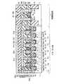
図65は、本発明の第10の実施形態に係る強誘電体記憶装置の断面図を示す。図65に示すように、第10の実施形態において、上記第3の実施形態と異なる点は、キャパシタ29a,29b,29c,29dが3次元キャパシタ構造になっている点である。つまり、下部電極26の上面及び側面に強誘電体膜27が形成され、この強誘電体膜27の上面及び側面に上部電極28が形成されることで、強誘電体膜27及び上部電極28がXYZ方向に延在している。 FIG. 65 is a sectional view of a ferro-electric memory device according to the tenth embodiment of the present invention. As shown in FIG. 65, the tenth embodiment is different from the third embodiment in that
尚、第10の実施形態においても、上記式(3),(4)の関係を満たした構造になっている。 In the tenth embodiment, the structure satisfies the relationships of the above formulas (3) and (4).
上記第10の実施形態によれば、上記第3の実施形態と同様の効果を得ることができる。さらに、3次元キャパシタを用いることで、キャパシタ容量を増大できるという効果も得られる。 According to the tenth embodiment, the same effects as in the third embodiment can be obtained. Further, the use of a three-dimensional capacitor can also provide an effect that the capacitor capacity can be increased.
尚、第10の実施形態では、第2及び第3のセル間を導通させるために、常にオンとなる埋め込みトランジスタTrfを設けているが、第4の実施形態のように、このトランジスタTrfを設けずに、第2の及び第3のセルキャパシタ下の拡散層を一続きに連続させてもよい。 In the tenth embodiment, the embedded transistor Trf that is always turned on is provided to make the second and third cells conductive. However, as in the fourth embodiment, the transistor Trf is provided. Instead, the diffusion layers under the second and third cell capacitors may be continuous.
[第11の実施形態]
第11の実施形態は、上記第10の実施形態における3次元キャパシタの形状を変形させたものである。[Eleventh embodiment]
In the eleventh embodiment, the shape of the three-dimensional capacitor in the tenth embodiment is modified.
図66は、本発明の第11の実施形態に係る強誘電体記憶装置の断面図を示す。図66に示すように、第11の実施形態において、上記第10の実施形態と異なる点は、3次元キャパシタ29a,29b,29c,29dの形状である。つまり、第10の実施形態では、強誘電体膜27及び上部電極28をXYZ方向に延在させているのに対し、第11の実施形態では、下部電極26及び強誘電体膜27をXYZ方向に延在させている。 FIG. 66 is a sectional view of a ferro-electric memory device according to the eleventh embodiment of the present invention. As shown in FIG. 66, the eleventh embodiment is different from the tenth embodiment in the shapes of three-
尚、第11の実施形態においても、上記式(3),(4)の関係を満たした構造になっている。 In the eleventh embodiment, the structure satisfies the relationships of the above formulas (3) and (4).
上記第11の実施形態によれば、上記第3の実施形態と同様の効果を得ることができる。さらに、3次元キャパシタを用いることで、キャパシタ容量を増大できるという効果も得られる。 According to the eleventh embodiment, the same effect as in the third embodiment can be obtained. Further, the use of a three-dimensional capacitor can also provide an effect that the capacitor capacity can be increased.
尚、第11の実施形態では、第2及び第3のセル間を導通させるために、常にオンとなる埋め込みトランジスタTrfを設けているが、第4の実施形態のように、このトランジスタTrfを設けずに、第2の及び第3のセルキャパシタ下の拡散層を一続きに連続させてもよい。 In the eleventh embodiment, the embedded transistor Trf that is always turned on is provided to make the second and third cells conductive. However, as in the fourth embodiment, the transistor Trf is provided. Instead, the diffusion layers under the second and third cell capacitors may be continuous.
[第12の実施形態]
第12の実施形態は、上記第10の実施形態において、ビット線とブロック選択トランジスタとの接続構造と、キャパシタの上部電極とソース/ドレインとの接続構造とを変形させたものである。[Twelfth embodiment]
The twelfth embodiment is obtained by modifying the connection structure between the bit line and the block selection transistor and the connection structure between the upper electrode of the capacitor and the source / drain in the tenth embodiment.
図67は、本発明の第12の実施形態に係る強誘電体記憶装置の断面図を示す。図67に示すように、第12の実施形態において、上記図65の第10の実施形態と異なる点は、(1)ビット線35aとブロック選択トランジスタTreのソース/ドレインとを、キャパシタ29eの下部電極26を介して接続している点と、(2)キャパシタ29a,29b,29c,29dの上部電極28とソース/ドレインとを、キャパシタ29f,29gの下部電極26を介してそれぞれ接続している点である。具体的には次のような構造になっている。 FIG. 67 is a sectional view of a ferro-electric memory device according to the twelfth embodiment of the present invention. As shown in FIG. 67, the twelfth embodiment differs from the tenth embodiment of FIG. 65 in that (1) the
ゲート電極16eの右側に位置する拡散層23上にコンタクト用の3次元キャパシタ29eが配置され、ゲート電極16a,16b間に位置する拡散層23上にコンタクト用の3次元キャパシタ29fが配置され、ゲート電極16c,16d間に位置する拡散層23上にコンタクト用の3次元キャパシタ29gが配置されている。ここで、コンタクト用のキャパシタ29e,29f,29gは、セルキャパシタ29a,29b,29c,29dと同じ構造になっている。 A contact three-
そして、コンタクト用のキャパシタ29e,29f,29gの下部電極26に、上部電極28及び強誘電体膜27を貫通するコンタクト31a,31c,31fがそれぞれ接続されている。 The
このようにして、ブロック選択トランジスタTreのソース/ドレインは、キャパシタ29eの下部電極26を介して、ビット線35aに接続されている。また、キャパシタ29a,29bの上部電極28は、キャパシタ29fの下部電極26を介して、トランジスタTra,Trbのソース/ドレインに接続されている。また、キャパシタ29c,29dの上部電極28は、キャパシタ29gの下部電極26を介して、トランジスタTrc,Trdのソース/ドレインに接続されている。 In this way, the source / drain of the block selection transistor Tre is connected to the
尚、第12の実施形態においても、上記式(3),(4)の関係を満たした構造になっている。 In the twelfth embodiment, the structure satisfies the relationships of the above formulas (3) and (4).
上記第12の実施形態によれば、上記第10の実施形態と同様の効果を得ることができる。さらに、ビット線35aとブロック選択トランジスタTreのソース/ドレインとの接続や、キャパシタ29a,29b,29c,29dの上部電極28とセルトランジスタTra,Trb,Trc,Trdのソース/ドレインとの接続に、キャパシタ29e,29f,29gの下部電極を用いることで、コンタクト31a,31c,31f下に下部電極26が存在することから、コンタクト31a,31c,31fの開口時に入るダメージを酸素雰囲気のアニールで回復でき、より信頼性の高い強誘電体キャパシタを提供できるという効果も得ることができる。 According to the twelfth embodiment, the same effect as in the tenth embodiment can be obtained. Further, the connection between the
尚、第12の実施形態では、第2及び第3のセル間を導通させるために、常にオンとなる埋め込みトランジスタTrfを設けているが、第4の実施形態のように、このトランジスタTrfを設けずに、第2の及び第3のセルキャパシタ下の拡散層を一続きに連続させてもよい。 In the twelfth embodiment, an embedded transistor Trf that is always turned on is provided in order to make the second and third cells conductive. However, as in the fourth embodiment, this transistor Trf is provided. Instead, the diffusion layers under the second and third cell capacitors may be continuous.
[第13の実施形態]
第13の実施形態は、上記第12の実施形態における3次元キャパシタの形状を変形させたものである。[Thirteenth embodiment]
In the thirteenth embodiment, the shape of the three-dimensional capacitor in the twelfth embodiment is modified.
図68は、本発明の第13の実施形態に係る強誘電体記憶装置の断面図を示す。図68に示すように、第13の実施形態において、上記第3の実施形態と異なる点は、3次元キャパシタ29a,29b,29c,29d,29e,29f,29gの形状である。つまり、第12の実施形態では、強誘電体膜27及び上部電極28をXYZ方向に延在させているのに対し、第13の実施形態では、下部電極26及び強誘電体膜27をXYZ方向に延在させている。 FIG. 68 is a sectional view of a ferro-electric memory device according to the thirteenth embodiment of the present invention. As shown in FIG. 68, the thirteenth embodiment is different from the third embodiment in the shapes of three-
尚、第13の実施形態においても、上記式(3),(4)の関係を満たした構造になっている。 In the thirteenth embodiment, the structure satisfies the relationships of the above formulas (3) and (4).
上記第13の実施形態によれば、上記第12の実施形態と同様の効果を得ることができる。 According to the thirteenth embodiment, the same effect as in the twelfth embodiment can be obtained.
尚、第13の実施形態では、第2及び第3のセル間を導通させるために、常にオンとなる埋め込みトランジスタTrfを設けているが、第4の実施形態のように、このトランジスタTrfを設けずに、第2の及び第3のセルキャパシタ下の拡散層を一続きに連続させてもよい。 In the thirteenth embodiment, the embedded transistor Trf that is always turned on is provided in order to make the second and third cells conductive. However, as in the fourth embodiment, the transistor Trf is provided. Instead, the diffusion layers under the second and third cell capacitors may be continuous.
その他、本発明は、上記各実施形態に限定されるものではなく、実施段階ではその要旨を逸脱しない範囲で、種々に変形することが可能である。さらに、上記実施形態には種々の段階の発明が含まれており、開示される複数の構成要件における適宜な組み合わせにより種々の発明が抽出され得る。例えば、実施形態に示される全構成要件から幾つかの構成要件が削除されても、発明が解決しようとする課題の欄で述べた課題が解決でき、発明の効果の欄で述べられている効果が得られる場合には、この構成要件が削除された構成が発明として抽出され得る。 In addition, the present invention is not limited to the above-described embodiments, and various modifications can be made without departing from the scope of the invention when it is practiced. Furthermore, the above embodiments include inventions at various stages, and various inventions can be extracted by appropriately combining a plurality of disclosed constituent elements. For example, even if some constituent requirements are deleted from all the constituent requirements shown in the embodiment, the problem described in the column of the problem to be solved by the invention can be solved, and the effect described in the column of the effect of the invention Can be obtained as an invention.
11…半導体基板、12…ストッパー絶縁膜、13…素子分離絶縁膜、14…ゲート溝、15,19…ゲート絶縁膜、16a,16b,16c…埋め込みゲート電極、17…埋め込み絶縁膜、18…低濃度拡散層、20…ゲート電極、21…低濃度拡散層、22…スペーサ、23…低濃度拡散層、24,25…層間膜、26…下部電極、27…強誘電体膜、28…上部電極、29a,29b…強誘電体キャパシタ、30,30a,30b,33…層間絶縁膜、31a,31b,31c,31d,31e,31f,31g,31h,31i,34,34a,34b…コンタクト、32a,32b,32c,32d,32e,32f,35,35a,35b…配線、40,41…絶縁膜、42…拡散防止膜、43…キャパシタ溝、44…埋め込み材、45…マスク材、Tra,Trb,Trc,Trd,Tre,Trf,Trg…トランジスタ。 DESCRIPTION OF
Claims (5)
Translated fromJapanese前記半導体基板内に第1の方向に延在して形成され、第1の深さを有する第1の溝と、
前記半導体基板内に前記第1の溝を横切る第2の方向に延在して形成され、前記第1の深さより浅い第2の深さを有し、上部領域と下部領域とを備えた第2の溝と、
前記第1の溝内に埋め込まれた第1の素子分離絶縁膜と、
前記第2の溝の前記下部領域内に第1のゲート絶縁膜を介して形成された第1のゲート電極と、
前記第2の溝の前記上部領域内に形成された第1の絶縁膜と、
前記第2の溝における一方の側面側の前記半導体基板内に形成された第1の拡散層と、
前記第2の溝における他方の側面側の前記半導体基板内に形成された第2の拡散層と、
前記第1の拡散層上に配置され、第1の下部電極と第1の強誘電体膜と第1の上部電極とを有する第1の強誘電体キャパシタと、
前記第1の強誘電体キャパシタ上に配置された第1のコンタクトと、
前記第1のコンタクト上に配置された第1の配線層と、
前記第2の拡散層上に配置された第2のコンタクトと、
前記第2のコンタクト上に配置され、第1の配線層と同一レベルに配置された第2の配線層と
を具備することを特徴とする強誘電体記憶装置。A semiconductor substrate;
A first groove formed in the semiconductor substrate extending in a first direction and having a first depth;
A second extension formed in the semiconductor substrate extending in a second direction across the first trench, having a second depth shallower than the first depth, and comprising an upper region and a lower region. Two grooves,
A first element isolation insulating film embedded in the first trench;
A first gate electrode formed in the lower region of the second trench via a first gate insulating film;
A first insulating film formed in the upper region of the second groove;
A first diffusion layer formed in the semiconductor substrate on one side of the second groove;
A second diffusion layer formed in the semiconductor substrate on the other side of the second groove;
A first ferroelectric capacitor disposed on the first diffusion layer and having a first lower electrode, a first ferroelectric film, and a first upper electrode;
A first contact disposed on the first ferroelectric capacitor;
A first wiring layer disposed on the first contact;
A second contact disposed on the second diffusion layer;
A ferroelectric memory device comprising: a second wiring layer disposed on the second contact and disposed at the same level as the first wiring layer.
前記第3の溝の前記下部領域内に第2のゲート絶縁膜を介して形成され、フィールドシールド領域として機能する第2のゲート電極と、
前記第3の溝の前記上部領域内に形成された第2の絶縁膜と
をさらに具備することを特徴とする請求項1に記載の強誘電体記憶装置。A third diffusion layer formed adjacent to the first diffusion layer in the semiconductor substrate and extending in the second direction, having the second depth, and comprising an upper region and a lower region; Groove,
A second gate electrode formed in the lower region of the third groove via a second gate insulating film and functioning as a field shield region;
The ferroelectric memory device according to claim 1, further comprising: a second insulating film formed in the upper region of the third groove.
前記第3の溝内に埋め込まれた第2の素子分離絶縁膜と
をさらに具備することを特徴とする請求項1に記載の強誘電体記憶装置。A third groove formed adjacent to the first diffusion layer and extending in the second direction in the semiconductor substrate and having the first depth;
The ferroelectric memory device according to claim 1, further comprising: a second element isolation insulating film embedded in the third trench.
前記第3の溝の前記下部領域内に第2のゲート絶縁膜を介して形成された第2のゲート電極と、
前記第3の溝の前記上部領域内に形成された第2の絶縁膜と、
前記第3の溝の前記第1の拡散層と反対側の側面の前記半導体基板内に形成された第3の拡散層と、
前記第3の拡散層上に配置され、前記第1の配線層に接続された第3のコンタクトと、
前記第3の拡散層と隣接して前記半導体基板内に前記第2の方向に延在して形成され、前記第2の深さを有し、上部領域と下部領域とを備えた第4の溝と、
前記第4の溝の前記下部領域内に第3のゲート絶縁膜を介して形成された第3のゲート電極と、
前記第4の溝の前記上部領域内に形成された第3の絶縁膜と、
前記第4の溝の前記第3の拡散層と反対側の側面の前記半導体基板内に形成された第4の拡散層と、
前記第4の拡散層上に配置され、第2の下部電極と第2の強誘電体膜と第2の部電極とを有する第2の強誘電体キャパシタと、
前記第2の強誘電体キャパシタ上に配置され、前記第1の配線層に接続された第4のコンタクトと
をさらに具備し、
第1のセルは、前記第1の強誘電体キャパシタと、前記第2のゲート電極と前記第1及び第3の拡散層とを有する第1のトランジスタとで構成され、
第2のセルは、前記第2の強誘電体キャパシタと、前記第3のゲート電極と前記第3及び第4の拡散層とを有する第2のトランジスタとで構成され、
前記第1の強誘電体キャパシタの一端は、前記第1の配線層、前記第1及び第3のコンタクトを介して前記第3の拡散層に電気的に接続され、前記第1の強誘電体キャパシタの他端は、前記第1の拡散層に電気的に接続され、
前記第2の強誘電体キャパシタの一端は、前記第1の配線層、前記第3及び第4のコンタクトを介して前記第3の拡散層に電気的に接続され、前記第2の強誘電体キャパシタの他端は、前記第4の拡散層に電気的に接続され、
前記第1のセルと前記第2のセルとは電気的に直列接続されていることを特徴とする請求項1に記載の強誘電体記憶装置。A third diffusion layer formed adjacent to the first diffusion layer in the semiconductor substrate and extending in the second direction, having the second depth, and comprising an upper region and a lower region; Groove,
A second gate electrode formed in the lower region of the third groove via a second gate insulating film;
A second insulating film formed in the upper region of the third groove;
A third diffusion layer formed in the semiconductor substrate on the side surface opposite to the first diffusion layer of the third groove;
A third contact disposed on the third diffusion layer and connected to the first wiring layer;
A fourth diffusion layer formed adjacent to the third diffusion layer and extending in the second direction in the semiconductor substrate, having the second depth, and having an upper region and a lower region; Groove,
A third gate electrode formed in the lower region of the fourth groove via a third gate insulating film;
A third insulating film formed in the upper region of the fourth groove;
A fourth diffusion layer formed in the semiconductor substrate on the side surface opposite to the third diffusion layer of the fourth groove;
A second ferroelectric capacitor disposed on the fourth diffusion layer and having a second lower electrode, a second ferroelectric film, and a second partial electrode;
A fourth contact disposed on the second ferroelectric capacitor and connected to the first wiring layer;
The first cell includes the first ferroelectric capacitor, the first transistor having the second gate electrode, and the first and third diffusion layers,
The second cell includes the second ferroelectric capacitor, the second transistor having the third gate electrode, and the third and fourth diffusion layers,
One end of the first ferroelectric capacitor is electrically connected to the third diffusion layer via the first wiring layer, the first and third contacts, and the first ferroelectric capacitor The other end of the capacitor is electrically connected to the first diffusion layer,
One end of the second ferroelectric capacitor is electrically connected to the third diffusion layer via the first wiring layer, the third and fourth contacts, and the second ferroelectric capacitor The other end of the capacitor is electrically connected to the fourth diffusion layer,
2. The ferroelectric memory device according to claim 1, wherein the first cell and the second cell are electrically connected in series.
前記第1の溝内に素子分離絶縁膜を形成する工程と、
前記半導体基板内に、前記第1の溝を横切る第2の方向に延在し、前記第1の深さより浅い第2の深さを有し、上部領域と下部領域とを備えた第2の溝を形成する工程と、
前記第2の溝の前記下部領域内にゲート絶縁膜を介してゲート電極を形成する工程と、
前記第2の溝の前記上部領域内に第1の絶縁膜を形成する工程と、
前記第2の溝における両側面の前記半導体基板内に第1及び第2の拡散層をそれぞれ形成する工程と、
前記第1の拡散層上に、第1の下部電極と第1の強誘電体膜と第1の上部電極とを有する第1の強誘電体キャパシタを形成する工程と、
前記第1の強誘電体キャパシタ上に第1のコンタクトを形成する工程と、
前記第2の拡散層上に第2のコンタクトを形成する工程と、
前記第1及び第2のコンタクト上に第1及び第2の配線層をそれぞれ形成する工程と
を具備することを特徴とする強誘電体記憶装置の製造方法。Forming a first groove extending in a first direction and having a first depth in the semiconductor substrate;
Forming an element isolation insulating film in the first trench;
A second extension extending in a second direction across the first trench in the semiconductor substrate, having a second depth shallower than the first depth, and comprising an upper region and a lower region. Forming a groove;
Forming a gate electrode through a gate insulating film in the lower region of the second trench;
Forming a first insulating film in the upper region of the second groove;
Forming first and second diffusion layers in the semiconductor substrate on both side surfaces of the second groove,
Forming a first ferroelectric capacitor having a first lower electrode, a first ferroelectric film, and a first upper electrode on the first diffusion layer;
Forming a first contact on the first ferroelectric capacitor;
Forming a second contact on the second diffusion layer;
Forming a first wiring layer and a second wiring layer on the first and second contacts, respectively. A method of manufacturing a ferroelectric memory device, comprising:
Priority Applications (2)
| Application Number | Priority Date | Filing Date | Title |
|---|---|---|---|
| JP2003408646AJP2005174977A (en) | 2003-12-08 | 2003-12-08 | Ferroelectric memory device and manufacturing method thereof |
| US10/933,382US7091537B2 (en) | 2003-12-08 | 2004-09-03 | Ferroelectric memory device and method of manufacturing the same |
Applications Claiming Priority (1)
| Application Number | Priority Date | Filing Date | Title |
|---|---|---|---|
| JP2003408646AJP2005174977A (en) | 2003-12-08 | 2003-12-08 | Ferroelectric memory device and manufacturing method thereof |
Publications (1)
| Publication Number | Publication Date |
|---|---|
| JP2005174977Atrue JP2005174977A (en) | 2005-06-30 |
Family
ID=34631788
Family Applications (1)
| Application Number | Title | Priority Date | Filing Date |
|---|---|---|---|
| JP2003408646APendingJP2005174977A (en) | 2003-12-08 | 2003-12-08 | Ferroelectric memory device and manufacturing method thereof |
Country Status (2)
| Country | Link |
|---|---|
| US (1) | US7091537B2 (en) |
| JP (1) | JP2005174977A (en) |
Cited By (5)
| Publication number | Priority date | Publication date | Assignee | Title |
|---|---|---|---|---|
| JP2008085178A (en)* | 2006-09-28 | 2008-04-10 | Toshiba Corp | Semiconductor device and manufacturing method thereof |
| JP2014057104A (en)* | 2013-12-16 | 2014-03-27 | Fujitsu Semiconductor Ltd | Semiconductor device and manufacturing method of the same |
| KR20160145811A (en)* | 2014-04-28 | 2016-12-20 | 마이크론 테크놀로지, 인크. | Ferroelectric memory and methods of forming the same |
| JP2017228616A (en)* | 2016-06-21 | 2017-12-28 | 富士通セミコンダクター株式会社 | Ferroelectric memory device |
| CN111863820A (en)* | 2019-04-25 | 2020-10-30 | 台湾积体电路制造股份有限公司 | Integrated wafer and method of forming integrated wafer |
Families Citing this family (11)
| Publication number | Priority date | Publication date | Assignee | Title |
|---|---|---|---|---|
| JP4371005B2 (en)* | 2004-08-12 | 2009-11-25 | セイコーエプソン株式会社 | Semiconductor device manufacturing method and semiconductor device |
| KR100672673B1 (en)* | 2004-12-29 | 2007-01-24 | 동부일렉트로닉스 주식회사 | Capacitor Structure and Manufacturing Method Thereof |
| JP5060413B2 (en)* | 2008-07-15 | 2012-10-31 | 株式会社東芝 | Semiconductor memory device |
| JP2010080628A (en)* | 2008-09-25 | 2010-04-08 | Toshiba Corp | Semiconductor memory and its production process |
| JP2012234964A (en) | 2011-04-28 | 2012-11-29 | Elpida Memory Inc | Semiconductor device and manufacturing method of the same |
| KR101929478B1 (en)* | 2012-04-30 | 2018-12-14 | 삼성전자주식회사 | Semiconductor Device Having a Buried Channel Array |
| JP2014022388A (en)* | 2012-07-12 | 2014-02-03 | Ps4 Luxco S A R L | Semiconductor device and method for manufacturing the same |
| US8796751B2 (en) | 2012-11-20 | 2014-08-05 | Micron Technology, Inc. | Transistors, memory cells and semiconductor constructions |
| US9847337B1 (en)* | 2016-12-27 | 2017-12-19 | Micron Technology, Inc. | Memory arrays comprising ferroelectric capacitors |
| JP2019179827A (en)* | 2018-03-30 | 2019-10-17 | ソニーセミコンダクタソリューションズ株式会社 | Semiconductor memory device and product-sum operation device |
| US11501812B2 (en)* | 2020-07-31 | 2022-11-15 | Taiwan Semiconductor Manufacturing Co., Ltd. | Semiconductor devices including ferroelectric memory and methods of forming the same |
Family Cites Families (5)
| Publication number | Priority date | Publication date | Assignee | Title |
|---|---|---|---|---|
| JP3311070B2 (en) | 1993-03-15 | 2002-08-05 | 株式会社東芝 | Semiconductor device |
| JP2669364B2 (en) | 1994-10-21 | 1997-10-27 | 日本電気株式会社 | Semiconductor memory device and manufacturing method thereof |
| JP3604254B2 (en) | 1997-03-25 | 2004-12-22 | 株式会社東芝 | Method for manufacturing semiconductor memory device |
| DE19805712A1 (en)* | 1998-02-12 | 1999-08-26 | Siemens Ag | Memory cell arrangement and corresponding manufacturing method |
| JP4481464B2 (en) | 2000-09-20 | 2010-06-16 | 株式会社東芝 | Semiconductor memory device and manufacturing method thereof |
- 2003
- 2003-12-08JPJP2003408646Apatent/JP2005174977A/enactivePending
- 2004
- 2004-09-03USUS10/933,382patent/US7091537B2/ennot_activeExpired - Fee Related
Cited By (9)
| Publication number | Priority date | Publication date | Assignee | Title |
|---|---|---|---|---|
| JP2008085178A (en)* | 2006-09-28 | 2008-04-10 | Toshiba Corp | Semiconductor device and manufacturing method thereof |
| US7821047B2 (en) | 2006-09-28 | 2010-10-26 | Kabushiki Kaisha Toshiba | Semiconductor apparatus and method for manufacturing the same |
| JP2014057104A (en)* | 2013-12-16 | 2014-03-27 | Fujitsu Semiconductor Ltd | Semiconductor device and manufacturing method of the same |
| KR20160145811A (en)* | 2014-04-28 | 2016-12-20 | 마이크론 테크놀로지, 인크. | Ferroelectric memory and methods of forming the same |
| JP2017518632A (en)* | 2014-04-28 | 2017-07-06 | マイクロン テクノロジー, インク. | Ferroelectric memory and method for forming the same |
| KR101965941B1 (en)* | 2014-04-28 | 2019-04-04 | 마이크론 테크놀로지, 인크. | Ferroelectric memory and methods of forming the same |
| US10707220B2 (en) | 2014-04-28 | 2020-07-07 | Micron Technology, Inc. | Ferroelectric memory and methods of forming the same |
| JP2017228616A (en)* | 2016-06-21 | 2017-12-28 | 富士通セミコンダクター株式会社 | Ferroelectric memory device |
| CN111863820A (en)* | 2019-04-25 | 2020-10-30 | 台湾积体电路制造股份有限公司 | Integrated wafer and method of forming integrated wafer |
Also Published As
| Publication number | Publication date |
|---|---|
| US20050121709A1 (en) | 2005-06-09 |
| US7091537B2 (en) | 2006-08-15 |
Similar Documents
| Publication | Publication Date | Title |
|---|---|---|
| US8344517B2 (en) | Integrated circuit devices including air spacers separating conductive structures and contact plugs and methods of fabricating the same | |
| KR100337587B1 (en) | Semiconductor device | |
| US6930347B2 (en) | Semiconductor memory device having electrical connection by side contact | |
| KR100375428B1 (en) | Semiconductor storage device and process for manufacturing the same | |
| US9236501B2 (en) | Dummy bit line MOS capacitor and device using the same | |
| KR100669928B1 (en) | Semiconductor device and manufacturing method thereof | |
| US11251188B2 (en) | Semiconductor memory device and a method of fabricating the same | |
| JP5717943B2 (en) | Semiconductor device and manufacturing method thereof | |
| KR100791339B1 (en) | Composite chip semiconductor device including planarization resistance pattern and manufacturing method | |
| KR970003953A (en) | Highly Integrated DRAM Cells and Manufacturing Method Thereof | |
| US20110260288A1 (en) | Semiconductor device and method for manufacturing the same | |
| KR100325472B1 (en) | Manufacturing Method of DRAM Memory Cells | |
| KR19980041982A (en) | Semiconductor integrated circuit device and manufacturing method thereof | |
| JP2005174977A (en) | Ferroelectric memory device and manufacturing method thereof | |
| US9685448B2 (en) | Semiconductor device | |
| US12096615B2 (en) | Semiconductor devices having contact plugs | |
| TW202236611A (en) | Semiconductor device | |
| US7511328B2 (en) | Semiconductor device having raised cell landing pad and method of fabricating the same | |
| US8999827B2 (en) | Semiconductor device manufacturing method | |
| WO2002056383A1 (en) | Semiconductor storage device and its manufacturing method | |
| US20080230818A1 (en) | Non-volatile memory device | |
| CN116896867A (en) | semiconductor memory device | |
| JP2007103652A (en) | Semiconductor device and manufacturing method thereof | |
| JP2005252283A (en) | Semiconductor device and manufacturing method thereof | |
| KR100576083B1 (en) | Semiconductor device and manufacturing method thereof |
Legal Events
| Date | Code | Title | Description |
|---|---|---|---|
| A977 | Report on retrieval | Free format text:JAPANESE INTERMEDIATE CODE: A971007 Effective date:20051102 | |
| A131 | Notification of reasons for refusal | Free format text:JAPANESE INTERMEDIATE CODE: A131 Effective date:20051129 | |
| A521 | Request for written amendment filed | Free format text:JAPANESE INTERMEDIATE CODE: A523 Effective date:20060127 | |
| A02 | Decision of refusal | Free format text:JAPANESE INTERMEDIATE CODE: A02 Effective date:20061219 |