JP2005159200A - Solid-state imaging device and manufacturing method thereof - Google Patents
Solid-state imaging device and manufacturing method thereofDownload PDFInfo
- Publication number
- JP2005159200A JP2005159200AJP2003398544AJP2003398544AJP2005159200AJP 2005159200 AJP2005159200 AJP 2005159200AJP 2003398544 AJP2003398544 AJP 2003398544AJP 2003398544 AJP2003398544 AJP 2003398544AJP 2005159200 AJP2005159200 AJP 2005159200A
- Authority
- JP
- Japan
- Prior art keywords
- color filter
- filter layer
- state imaging
- imaging device
- solid
- Prior art date
- Legal status (The legal status is an assumption and is not a legal conclusion. Google has not performed a legal analysis and makes no representation as to the accuracy of the status listed.)
- Granted
Links
Images


Classifications
- H—ELECTRICITY
- H10—SEMICONDUCTOR DEVICES; ELECTRIC SOLID-STATE DEVICES NOT OTHERWISE PROVIDED FOR
- H10F—INORGANIC SEMICONDUCTOR DEVICES SENSITIVE TO INFRARED RADIATION, LIGHT, ELECTROMAGNETIC RADIATION OF SHORTER WAVELENGTH OR CORPUSCULAR RADIATION
- H10F39/00—Integrated devices, or assemblies of multiple devices, comprising at least one element covered by group H10F30/00, e.g. radiation detectors comprising photodiode arrays
- H10F39/80—Constructional details of image sensors
- H10F39/805—Coatings
- H10F39/8053—Colour filters
- H—ELECTRICITY
- H10—SEMICONDUCTOR DEVICES; ELECTRIC SOLID-STATE DEVICES NOT OTHERWISE PROVIDED FOR
- H10F—INORGANIC SEMICONDUCTOR DEVICES SENSITIVE TO INFRARED RADIATION, LIGHT, ELECTROMAGNETIC RADIATION OF SHORTER WAVELENGTH OR CORPUSCULAR RADIATION
- H10F39/00—Integrated devices, or assemblies of multiple devices, comprising at least one element covered by group H10F30/00, e.g. radiation detectors comprising photodiode arrays
- H10F39/80—Constructional details of image sensors
- H10F39/806—Optical elements or arrangements associated with the image sensors
- H10F39/8063—Microlenses
Landscapes
- Solid State Image Pick-Up Elements (AREA)
- Transforming Light Signals Into Electric Signals (AREA)
- Optical Filters (AREA)
- Color Television Image Signal Generators (AREA)
Abstract
Description
Translated fromJapanese本発明はオンチップカラーフィルタを有する固体撮像装置とその製造方法に関するものである。 The present invention relates to a solid-state imaging device having an on-chip color filter and a manufacturing method thereof.
近年、固体撮像装置、CCD(Charge Coupled Device)型をはじめとする固体撮像装置では、小型化、高画素化が進んでいる。しかし、 従来のオンチップカラーフィルタを有する固体撮像装置は受光センサ部であるフォトダイオードの受光面積を縮小させる結果、固体撮像装置の主要特性である光電変換特性(光感度)を低下させる一因となりつつある。 In recent years, solid-state imaging devices such as a solid-state imaging device and a CCD (Charge Coupled Device) type have been reduced in size and increased in pixels. However, the conventional solid-state imaging device having the on-chip color filter reduces the light receiving area of the photodiode that is the light receiving sensor unit, and as a result, decreases the photoelectric conversion characteristic (photosensitivity) that is the main characteristic of the solid-state imaging device. It's getting on.
例えば、デジタルスチルカメラに搭載される固体撮像装置の光学サイズの主流は1/3インチ型から1/4インチ型が主流となり、更には1/6インチ型以降の検討もなされている。又、画素数も200万画素から500万画素の範囲まで広がりつつあり、更には500万画素以上の検討もなされている。こうした受光面積の縮小化、及び高画素化においても、固体撮像装置の主要特性である、光感度、及び隣接画素との混色、ライン濃淡などの特性を低下させることのない技術の確立が必要となってきている。 For example, the mainstream of the optical size of a solid-state imaging device mounted on a digital still camera is a 1/3 inch type to a 1/4 inch type, and further studies on a 1/6 inch type and later are also being made. Also, the number of pixels is expanding from 2 million pixels to 5 million pixels, and more than 5 million pixels have been studied. Even in the reduction of the light receiving area and the increase in the number of pixels, it is necessary to establish a technology that does not deteriorate the main characteristics of the solid-state imaging device, such as light sensitivity, color mixing with adjacent pixels, and line shading. It has become to.
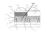
図5は特許文献1等に開示された固体撮像装置の画素部分の断面図である。この固体撮像装置は、第一導電型、例えばN型シリコン半導体からなる半導体基板1に第二導電型となるP型の第一の半導体ウエル領域2が形成され、この第一のP型半導体ウエル領域2にマトリックス配列の各受光センサ部3を構成するための、N型半導体領域が形成される。
更に、ゲート絶縁膜4を介して、例えば多結晶シリコンからなる転送電極5が形成される。転送電極5上を被覆する層間絶縁膜6を介して受光センサ部3の開口を除く他部全面に、例えばAL、Wなどによる遮光膜7が形成され、その後表面保護膜8で覆われる。FIG. 5 is a cross-sectional view of a pixel portion of the solid-state imaging device disclosed in
Further, a
更に、第1の透明平坦化膜9、カラーフィルタ層10G、10B、第2の透明平坦化膜11を順次形成し、この平坦化膜11上に各受光センサ部3への入射光を集光する、オンチップマイクロレンズ12が形成される。
第1の透明平坦化膜9は、安定したカラーフィルタ層を形成するため、下地の段差をなくすための膜である。第2の透明平坦化膜11は、精度よくオンチップマイクロレンズ12を形成するために、下地のカラーフィルタ層10上を平坦にするための膜である。Further, a first transparent
The first transparent
カラーフィルタ層10としては、補色のイエロー、シアン、マゼンタ、グリーン(単独、またはイエローとシアンを重ねて形成)からなるカラーフィルタ、または原色のレッド、グリーン、ブルーから成るカラーフィルタ等で構成される。
従来カラーフィルタ層は、例えば、染色法、或いは染料、顔料を含有したフォトレジスト膜を選択露光、現像処理を施し目的のフィルタを形成するカラーレジスト法で形成される。The
Conventional color filter layers are formed by, for example, a dyeing method or a color resist method in which a photoresist film containing a dye and a pigment is selectively exposed and developed to form a target filter.
特許文献1に開示された改善例によれば、微細化により、特に斜め光からの光感度低下、隣接画素による混色防止の対策として、半導体基板表面から第2の透明平坦化膜11までの距離を短くすることが必須であり、その手段としてシアンとイエローを重ね合わせて形成するためカラーフィルタ層の中で最も厚膜となる可能性の高い、補色グリーンフィルタの薄膜化を提案している。 According to the improved example disclosed in
その一実施例として、カラーフィルタの製造方法において、一色目のカラーフィルタ成分で感光材成分を含まないカラーフィルタ被膜を選択エッチングして形成するので、例えば補色カラーフィルタを製造するときは、グリーンフィルタ成分をこの一色目の方法で形成すれば、グリーンフィルタ成分を他の色のフィルタ成分と同じように薄い膜厚で形成でき、従って、カラーフィルタ層の薄膜化が図られる。
従来の固体撮像装置では画素サイズの縮小に対し、半導体基板から第2の透明平坦化膜11までの距離を短くする工夫が提案され、受光センサ部3の垂直に入射する光に対してはある程度の効果が期待されている。しかしながら、斜め光に対してはカラーフィルタ層10の形状による要因が大きく、構造上斜め方向から入射した光は隣接するカラーフィルタ層を透過し受光センサ部3に入射することにより混色をもたらし、必要とする分光特性が得られない。さらに、光の入射角度により混色の度合いが変わり、ライン濃淡、感度バラツキ等の課題を解決するには至っていない。 In the conventional solid-state imaging device, a device for shortening the distance from the semiconductor substrate to the second transparent flattening film 11 is proposed for reducing the pixel size. The effect is expected. However, for oblique light, the factor due to the shape of the
上記課題に鑑み本発明は、カラーフィルタ層の形状を改善することにより、隣接するカラーフィルタ層からの混色、ライン濃淡、感度バラツキを低減させ、微細化を可能にする固体撮像装置及びその製造方法を提供することを目的とする。 In view of the above problems, the present invention improves the shape of a color filter layer, thereby reducing color mixing, line shading, and sensitivity variation from adjacent color filter layers, and a solid-state imaging device that enables miniaturization and a method for manufacturing the same The purpose is to provide.
上記課題を解決するため本発明の固体撮像装置は、半導体基板上に形成された光電変換素子と前記光電変換素子の上に形成されたカラーフィルタ層とを有する画素が、複数配列された固体撮像装置であって、前記カラーフィルタ層のそれぞれの膜厚は周辺部よりも中央部が厚いことを特徴とする。これにより、斜め光に対し隣接するカラーフィルタ層からの影響を受けにくく、混色防止、ライン濃淡の改善、感度バラツキの低減が可能である。
なお、前記カラーフィルタ層は、画素部よりも狭い寸法で形成された第1のカラーフィルタ層と、画素部と同じ寸法で形成した第2のカラーフィルタ層を積層して形成されるものであって良い。
また、第1のカラーフィルタ層と第2のカラーフィルタ層は同一材料にて形成することで均一なレンズ構造とすることができる。In order to solve the above problems, a solid-state imaging device according to the present invention provides a solid-state imaging in which a plurality of pixels each having a photoelectric conversion element formed on a semiconductor substrate and a color filter layer formed on the photoelectric conversion element are arranged. An apparatus is characterized in that the film thickness of each of the color filter layers is thicker at the center than at the periphery. Thereby, it is difficult to be influenced by the adjacent color filter layer with respect to the oblique light, and it is possible to prevent color mixing, improve line shading, and reduce sensitivity variation.
The color filter layer is formed by laminating a first color filter layer formed with a size smaller than that of the pixel portion and a second color filter layer formed with the same size as the pixel portion. Good.
In addition, the first color filter layer and the second color filter layer can be formed of the same material to obtain a uniform lens structure.
また、第1のカラーフィルタと第2のカラーフィルタとは色素濃度が異なることを特徴とする。色素濃度を調整することで斜め入射光と垂直入射光の分光特性をそろえることができ色むらを防止することができる。
また、さらに光電変換素子とカラーフィルタ層との間に第1の透明膜を有し、前記カラーフィルタ層は、第1の透明膜よりも屈折率が大きいことを特徴とする。
また、さらにカラーフィルタ層の上に第2の透明膜を有し、前記第2の透明膜は、前記カラーフィルタ層よりも屈折率が小さいことを特徴とする。
また、さらに第2の透明膜上にマイクロレンズを有し、前記マイクロレンズは、前記第2の透明膜よりも大きな屈折率を有することを特徴とする。
上記構成によれば、さらにレンズの集光効果を高め、集光効率を高めることが可能である。Further, the first color filter and the second color filter have different dye concentrations. By adjusting the dye concentration, the spectral characteristics of obliquely incident light and perpendicularly incident light can be made uniform, and uneven color can be prevented.
Further, the first transparent film is further provided between the photoelectric conversion element and the color filter layer, and the color filter layer has a refractive index larger than that of the first transparent film.
Further, a second transparent film is further provided on the color filter layer, and the second transparent film has a refractive index smaller than that of the color filter layer.
Furthermore, a microlens is further provided on the second transparent film, and the microlens has a refractive index larger than that of the second transparent film.
According to the above configuration, it is possible to further improve the light condensing effect of the lens and increase the light condensing efficiency.
さらに、前記固体撮像装置は、前記カラーフィルタ上に、第2の透明平坦化膜11を介して上に凸状のマイクロレンズを備える構成としてもよい。
上記構成によれば、カラーフィルタ層のレンズ効果に加えて、その上にマイクロレンズを備えることで、より集光率を向上させ、感度を向上させることができる。Furthermore, the solid-state imaging device may be configured to include a convex microlens on the color filter via a second transparent planarization film 11.
According to the said structure, in addition to the lens effect of a color filter layer, a condensing rate can be improved more and a sensitivity can be improved by providing a micro lens on it.
ここで、マイクロレンズの屈折率については、カラーフィルタ層がマイクロレンズよりも大きい構成とすることが好ましい。
この構成によれば、2層のマイクロレンズによって段階的に効率よく集光することができ、感度の向上が期待できる。
また、本発明の固体撮像装置の製造方法は、半導体基板上に形成された光電変換素子と前記光電変換素子の上に形成されたカラーフィルタ層とを有する画素が、複数配列された固体撮像装置の製造方法であって、カラーフィルタ層は、画素部よりも狭い寸法で第1のカラーフィルタ層を形成する工程と、第1のカラーフィルタ層の上に画素部と同じ寸法で第2のカラーフィルタ層を形成する工程とを有することを特徴とする。Here, with respect to the refractive index of the microlens, the color filter layer is preferably larger than the microlens.
According to this configuration, the two-layer microlens can efficiently collect light in steps, and an improvement in sensitivity can be expected.
The solid-state imaging device manufacturing method of the present invention is a solid-state imaging device in which a plurality of pixels each having a photoelectric conversion element formed on a semiconductor substrate and a color filter layer formed on the photoelectric conversion element are arranged. The color filter layer includes a step of forming the first color filter layer with a size narrower than that of the pixel portion, and a second color with the same size as the pixel portion on the first color filter layer. And a step of forming a filter layer.
さらに、同一マスクにてアンダー露光領域で露光することにより画素サイズよりも小さな第1のカラーフィルタ層を形成し、その後第2のカラーフィルタ層を適正またはオーバー露光領域で露光することによりマスク1枚にて積層カラーフィルタ層を形成することも可能である。 Further, a first color filter layer smaller than the pixel size is formed by exposing in the underexposed area with the same mask, and then one mask is formed by exposing the second color filter layer in an appropriate or overexposed area. It is also possible to form a laminated color filter layer.
以上説明したように、本発明の固体撮像装置によれば、カラーフィルタ層の中心部が周辺部よりも厚膜に形成することにより、斜め光に対し隣接するカラーフィルタ層からの影響を受けにくく、混色防止、ライン濃淡の改善、感度バラツキの低減が可能である。
また、各カラーフィルタ層を2回に分けて形成する積層構造とすることにより中心部より周辺部が薄膜化し、上に凸のレンズ形状を実現することができる。As described above, according to the solid-state imaging device of the present invention, the central part of the color filter layer is formed to be thicker than the peripheral part, so that it is less susceptible to the influence of the color filter layer adjacent to the oblique light. It is possible to prevent color mixing, improve line shading, and reduce sensitivity variation.
Further, by forming each color filter layer in two layers, the peripheral portion is made thinner than the central portion, and a convex lens shape can be realized.
また、中央部と周辺部に色の濃淡をつけることにより、斜め光と正面光との分光を一致させることができ、色ムラを低減させることができる。 In addition, by adding color shading to the central part and the peripheral part, it is possible to match the spectra of the oblique light and the front light, and to reduce color unevenness.
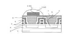
<固体撮像装置の構成>
図1は、本発明の一実施例に係る固体撮像装置の断面の構成を示す図である。同図では光電変換素子一つ分の断面を示している。
この固体撮像装置は、第一伝導型(例えばN型)の半導体基板1に第二伝導型(P型)の第一半導体ウエル2が形成され、この第一半導体ウエル2にマトリックス配列の各受光センサ部3を構成するための、N型半導体領域が形成されている。<Configuration of solid-state imaging device>
FIG. 1 is a diagram illustrating a cross-sectional configuration of a solid-state imaging device according to an embodiment of the present invention. The figure shows a cross section for one photoelectric conversion element.
In this solid-state image pickup device, a
さらに、ゲート絶縁膜4を介して多結晶シリコンからなる転送電極5、6、前記転送電極上を被覆する層間絶縁膜6を介して受光センサ部3の開口を除く他部全面に、AL等からなる遮光膜7が形成され、さらにSiON膜等からなる表面保護膜8が形成される。
前記転送電極と受光センサ3との間には凹凸ができている。その後形成するカラーフィルタ層10を精度よく形成するためにフェノール系樹脂等を主成分とする感光性透明膜を用い、周知の塗布、露光、現像工程により第1の透明平坦化膜9を形成する。Further, the
Unevenness is formed between the transfer electrode and the
その後、画素サイズよりも小さな設計により作成されたマスクを用い、塗布、露光、現像を行い、画素サイズよりも小さな第1のカラーフィルタ層13Gを作成し、連続して第1のカラーフィルタ層13G形成時よりも薄膜となる塗布条件にて同一カラーフィルタ材料を塗布後、画素サイズと同じ寸法にて設計されたマスクを用い、第2のカラーフィルタ層14Gを形成することにより、積層構造の上に凸のレンズ形状をしたカラーフィルタ層が得られる。 Thereafter, coating, exposure, and development are performed using a mask created by a design smaller than the pixel size to create a first
さらに、その後形成するオンチップマイクロレンズ12を精度よく形成するためにアクリル系透明樹脂を主成分とする透明膜を複数回塗布、ベーク後、エッチバックにより第2の透明平坦化膜11を形成後、前記オンチップマイクロレンズ12を塗布、露光、現像工程を経て形成する。
上記カラーフィルタ層は、上に凸のレンズ形状を有しているため、例えば、遮光膜7に向かう斜め入射光を集めることができ、受光サンサ部3の受光面への集効率を向上させ、感度を向上させることができる。さらに、隣接受光センサ上にある他のカラーフィルタ層の影響を受けないため、斜め入射光に対し混色を防止し、ライン濃淡、色ムラを低減できる。Further, in order to accurately form the on-
Since the color filter layer has an upwardly convex lens shape, for example, it is possible to collect oblique incident light toward the light-shielding
<固体撮像装置の製造工程>
図1に示した固体撮像装置の製造方法について、図2〜図4、及び図1を用いて説明する。図2、図1は固体撮像装置の断面を、主な製造工程の順に示す図である。<Manufacturing process of solid-state imaging device>
1 will be described with reference to FIGS. 2 to 4 and FIG. 2 and 1 are views showing cross sections of the solid-state imaging device in the order of main manufacturing steps.
図2はN型半導体基板1上に表面保護膜8までが形成された断面図である。同図に示す断面に至る製造工程を次の(1)〜(4)に説明する。
(1) N型半導体基板1上のPウエル層2、N型拡散層(受光センサ部3)は、一般にフォトリソ工程、イオン注入工程、熱拡散工程を繰り返して形成される。
(2)その後、ゲート絶縁膜4形成後、導電性多結晶シリコンからなる転送電極5、W等からなる遮光膜7が形成される。
(3)その後、例えば熱フロー処理によりBPSG膜(ホウ素−リンケイ酸ガラス)からなる表面保護膜8が形成される。
(4)さらに、アルミ等からなる配線(図外)を形成後、例えばSiON膜および電極取り出し用のボンディングパット(図外)が形成される。FIG. 2 is a sectional view in which up to the surface
(1) The
(2) Thereafter, after the
(3) Thereafter, the surface
(4) Further, after forming a wiring (not shown) made of aluminum or the like, for example, a SiON film and a bonding pad (not shown) for taking out the electrode are formed.
図3は、さらに緑色用第2のカラーフィルタ層14G形成後までの断面図を示す。同図に示す断面に至る製造工程を次の(5)〜(8)に説明する。
(5)表面保護膜上に、例えばフェノール系樹脂を主成分とする感光性透明樹脂を塗布し、露光、現像処理を施し受光センサ3上の窪みを埋める。
(6)その後、例えばアクリル系熱硬化型透明樹脂の薄膜を塗布、熱硬化するか、またはHMDS(ヘキサメチルジシラザン)膜の蒸気塗布後、緑色光用第1のカラーフィルタ層13Gを形成するためのレジストを塗布する。このレジストには、染料あるいは顔料が、例えば緑色系波長の光を選択的に透過するように調合されている。
(7)次いで、塗布されたカラーレジストを、受光センサ3上の緑色用カラーフィルタ層を形成する領域よりも小さな部分に残るように設計されたフォトマスクを用い、露光、現像を行う。例えば、緑色用カラーフィルタ層を形成する領域が2μm角の正方画素の場合、第1のカラーフィルタ層13Gは1.5μm程に仕上がるように形成する。
(8)連続して、前記同一カラーフィルタ材料を、前記第1のカラーフィルタ塗布時よりも薄く塗布し、受光センサ部3と同じサイズ(2μm角)に設計されたフォトマスクを用い、露光、現像を施し第2のカラーフィルタ層14Gを形成することにより、上に凸レンズ状で、かつ中央部が周辺部よりも濃い分光特性を併せ持った緑色用カラーフィルタ層を形成する。FIG. 3 is a cross-sectional view of the second
(5) A photosensitive transparent resin mainly composed of, for example, a phenolic resin is applied on the surface protective film, and exposure and development processes are performed to fill the depressions on the
(6) Thereafter, for example, a thin film of an acrylic thermosetting transparent resin is applied and thermoset, or after the vapor application of the HMDS (hexamethyldisilazane) film, the first
(7) Next, exposure and development are performed using a photomask designed so that the applied color resist remains in a portion smaller than the area where the green color filter layer is formed on the
(8) Continuously applying the same color filter material thinner than when applying the first color filter, and using a photomask designed to have the same size (2 μm square) as the light receiving
図4は、前記緑色カラーフィルタ形成後から、エッチバック前の平坦化膜が形成された断面図を示す。同図に示す断面に至る製造工程を次の(9)〜(10)に説明する。
(9)緑色用カラーフィルタ層形成後、同様の方法で赤色用カラーフィルタ層、青色用カラーフィルタ層をそれぞれの定められた位置に形成する。
(10)各カラーフィルタ層の上に、例えばアクリル系樹脂を主成分とする熱硬化性透明樹脂を複数回塗布、熱硬化を繰り返しカラーフィルタ形成後の表面を平坦化させる。FIG. 4 is a cross-sectional view in which a planarizing film is formed after the green color filter is formed and before etch back. The manufacturing steps leading to the cross section shown in the figure will be described in the following (9) to (10).
(9) After the green color filter layer is formed, the red color filter layer and the blue color filter layer are formed in the same positions by the same method.
(10) On each color filter layer, for example, a thermosetting transparent resin mainly composed of an acrylic resin is applied a plurality of times, and heat curing is repeated to flatten the surface after forming the color filter.
図1は、さらに、エッチバック後の平坦化膜形成からマイクロレンズ形成までの断面図を示す。同図に示す断面に至る製造工程を次の(11)〜(12)に説明する。
(11)感度向上を目的として、受光面から各カラーフィルタ層上の表面までの距離を短くするために、周知のエッチバック法により前記熱硬化性透明樹脂を可能な限り薄くエッチングを施す。
(12)その後、受光センサ3上にフェノール系樹脂を主成分とする感光性透明樹脂を塗布、露光、現像工程を経て上に凸状のオンチップマイクロレンズ12を形成する。
前記オンチップマイクロレンズ12は紫外線照射により透過率を高めている。なお、マイクロレンズのポストベーク温度は、カラーフィルタ層の分光特性の劣化を防ぐため、処理温度は200度以下にする必要がある。また、第1の透明平坦化膜9の屈折率はカラーフィルタ層の屈折率よりも低く、第2の透明平坦化膜11の屈折率は、前記カラーフィルタ層よりも低く、オンチップマイクロレンズ12の屈折率は前記第2の透明平坦化膜11よりも高くする必要がある。FIG. 1 further shows a cross-sectional view from the planarization film formation to the microlens formation after the etch back. The manufacturing process leading to the cross section shown in the figure will be described in the following (11) to (12).
(11) For the purpose of improving the sensitivity, the thermosetting transparent resin is etched as thinly as possible by a known etch back method in order to shorten the distance from the light receiving surface to the surface on each color filter layer.
(12) Thereafter, a photosensitive transparent resin mainly composed of a phenolic resin is applied onto the
The on-
上記工程により、図1に示した固体撮像装置を製造することができる。
以上説明してきたように、本発明の実施の形態における固体撮像装置によれば、カラーフィルタ層を第1のカラーフィルタ層と第2のカラーフィルタ層と2回に分けて形成するため、簡単に上凸レンズ形状のカラーフィルタ層が形成できる。その結果、斜め光による隣接カラーフィルタからの混色が防止でき、固体撮像装置として精細な画像を得ることができる。Through the above process, the solid-state imaging device shown in FIG. 1 can be manufactured.
As described above, according to the solid-state imaging device according to the embodiment of the present invention, the color filter layer is formed by dividing the color filter layer into the first color filter layer and the second color filter layer twice. An upward convex lens-shaped color filter layer can be formed. As a result, color mixing from adjacent color filters due to oblique light can be prevented, and a fine image can be obtained as a solid-state imaging device.
また、カラーフィルタ層が上凸レンズ形状をし、かつ屈折率が第1の平坦化膜よりも高いことから、入射光を効率良く受光センサ部3に集光することができ、その結果、感度を向上させることができる。
さらに、カラーフィルタ層周辺部での膜厚を薄膜化できることから、受光センサ部3上に精度良くカラーフィルタ層を形成できるため、各画素毎の色ムラがなくなり、その結果、固体撮像装置として、ライン濃淡、色シェーディング、が改善される。In addition, since the color filter layer has an upward convex lens shape and the refractive index is higher than that of the first planarization film, incident light can be efficiently collected on the light receiving
Furthermore, since the film thickness at the periphery of the color filter layer can be reduced, the color filter layer can be formed on the light receiving
また、カラーフィルタ層中心部に比べ、周辺部での分光が淡くなることから、従来構造に比べ、カラーフィルタ層周辺部からの透過光が増加し、その結果、固体撮像装置として、感度の向上が期待できる。
また、カラーフルタ膜上に形成する第2の透明平坦化膜11の屈折率は、上凸レンズ形状のカラーフィルタ層よりも低いため、前記カラーフィルタへの集光が効果的となり、感度の向上が期待できる。In addition, since the spectrum at the periphery is lighter than that at the center of the color filter layer, the transmitted light from the periphery of the color filter layer is increased compared to the conventional structure. As a result, the sensitivity of the solid-state imaging device is improved. Can be expected.
Further, since the refractive index of the second transparent flattening film 11 formed on the color filter film is lower than that of the color filter layer having an upward convex lens shape, the light condensing on the color filter becomes effective, and the sensitivity is improved. I can expect.
さらに、第2の透明平坦化膜11上に形成するオンチップマイクロレンズ12の屈折率は、前記第2の平坦化膜よりも高いため、マイクロレンズに入射する光を効率良く受光センサ部に集光することができ、その結果、感度の向上ができる。
なお、前記カラーフィルタ層の下に形成する透明平坦化膜を形成する手段としては、透明膜を塗布後、露光、現像を行い下地表面の凹を埋め込む方法、また、透明膜を複数回塗布後周知のエッチバックにより平坦化する方法、透明膜を塗布後、熱フロー処理により平坦化する方法、さらに、前記処理方法を複合してより平坦性を向上させる方法がある。Furthermore, since the refractive index of the on-
As a means for forming a transparent flattening film to be formed under the color filter layer, a method of embedding a recess on the underlying surface by applying exposure and development after applying the transparent film, or after applying the transparent film a plurality of times There are a well-known method of flattening by etch-back, a method of flattening by applying a transparent film and then heat-flowing, and a method of improving the flatness by combining the above processing methods.
前記カラーフィルタ層を2回に分けて形成する方法としては、第1のカラーフィルタ層を塗布後、画素サイズよりも小さなパターンで構成されるマスクを用い露光を行い、その後現像処理をして第1のカラーフィルタ層を形成後、前記同種類の材料を用いカラーフィルタ層を、前記第1のカラーフィルタ層と同じかそれよりも薄く塗布後、画素サイズと同等のマスクを用い露光を行い、その後現像処理を施し第2のカラーフィルタ層を形成することにより必要とする分光を備えたカラーフィルタ層を得る。 As a method for forming the color filter layer in two steps, after applying the first color filter layer, exposure is performed using a mask having a pattern smaller than the pixel size, and then development processing is performed. After forming the
また、第2のカラーフィルタ層を形成する場合、第1のカラーフィルタ層よりも色素濃度を変えてして形成する構成としてもよい。例えば、第1のカラーフィルタ層よりも色素濃度を薄くして形成して良い。
このような製造方法によれば、上記の構成、作用および効果を有する固体撮像装置を製造することができる。In addition, when the second color filter layer is formed, the second color filter layer may be formed by changing the dye concentration as compared with the first color filter layer. For example, the pigment concentration may be lower than that of the first color filter layer.
According to such a manufacturing method, a solid-state imaging device having the above-described configuration, operation, and effect can be manufactured.
以上、本発明の実施形態における固体撮像装置及び製造方法について説明したが、この発明は、本実施形態に限定されるものではなく、その趣旨を逸脱しない範囲で様々に変形することができる。
例えば、カラーフィルタ層の例として、色調が優先される固体撮像装置に用いられる原色方式について説明したが、解像度、感度が優先される固体撮像装置に用いられる補色方式としても良い。補色方式の場合には、カラーフィルタ層として、マゼンタ光用カラーフィルタ層、緑色光用カラーフィルタ層、黄色光用カラーフィルタ層、シアン光用カラーフィルタ層が周知の色配列におけるそれぞれの定められた位置に形成される。The solid-state imaging device and the manufacturing method according to the embodiment of the present invention have been described above. However, the present invention is not limited to the present embodiment, and various modifications can be made without departing from the spirit of the present invention.
For example, as an example of the color filter layer, the primary color method used for a solid-state imaging device in which color tone is given priority has been described, but a complementary color method used in a solid-state imaging device in which resolution and sensitivity are given priority may be used. In the case of the complementary color method, as the color filter layer, a magenta light color filter layer, a green light color filter layer, a yellow light color filter layer, and a cyan light color filter layer are respectively defined in known color arrangements. Formed in position.
また、カラーレジスト層を形成する材料としては、染料を含有したカラーレジスト、顔料を含有したカラーレジスト等あるが、いずれの選択も可能である。
また、第1の透明平坦化膜9の形成には感光性透明樹脂による、周知のフォトリソグラフィ技術について説明したが、熱硬化性樹脂材料を複数回塗布、熱硬化を繰り返し、周知のエッチバック法による形成方法もある。The material for forming the color resist layer includes a color resist containing a dye and a color resist containing a pigment, and any of these can be selected.
In addition, a well-known photolithography technique using a photosensitive transparent resin has been described for the formation of the first
また、第1の平坦化膜形成後、カラーレジスト材料との密着性を強化する目的で採用したアクリル系樹脂を主成分とする熱硬化型透明樹脂、またはHMDS膜は密着強度が保証されれば、省略が可能である。
また、上記実施例においてはCCD型の固体撮像装置として説明したが、これに限定されるものではなくMOS型等、他の固体撮像装置であっても適用可能である。In addition, after the first planarization film is formed, the thermosetting transparent resin or the HMDS film mainly composed of an acrylic resin employed for the purpose of strengthening the adhesion with the color resist material is guaranteed if the adhesion strength is guaranteed. It can be omitted.
In the above embodiment, the CCD type solid-state image pickup device has been described. However, the present invention is not limited to this, and other solid-state image pickup devices such as a MOS type can be applied.
本発明は、半導体基板上に形成された複数の光電変換素子と、その周囲に形成された転送電極と、光電変換素子上に形成されるカラーフィルタ層、さらにカラーフィルタ層上に形成されるマイクロレンズを有する固体撮像装置に適している。 The present invention relates to a plurality of photoelectric conversion elements formed on a semiconductor substrate, transfer electrodes formed around the photoelectric conversion elements, a color filter layer formed on the photoelectric conversion elements, and a micro formed on the color filter layer. It is suitable for a solid-state imaging device having a lens.
1 N型半導体基板
2 P型の第一半導体ウエル
3 受光センサ部(フォトダイオード)
4 ゲート絶縁膜
5 転送電極
6 層間絶縁膜
7 遮光膜
8 表面保護膜
9 第1の平坦化膜
10 カラーフィルタ層
11 第2の平坦化膜
12 マイクロレンズ
13G 緑色用第1のカラーフィルタ層
14G 緑色用第2のカラーフィルタ層1 N-type semiconductor substrate 2 P-type first semiconductor well 3 Light-receiving sensor portion (photodiode)
4
Claims (10)
Translated fromJapanese前記カラーフィルタ層は、前記画素よりも狭い寸法で第1のカラーフィルタ層を形成する工程と、
前記第1のカラーフィルタ層の上に前記画素と同じ寸法で第2のカラーフィルタ層を形成する工程と
を有する固体撮像装置の製造方法。A pixel having a photoelectric conversion element formed on a semiconductor substrate and a color filter layer formed on the photoelectric conversion element is a method for manufacturing a solid-state imaging device in which a plurality of pixels are arranged,
The color filter layer forming a first color filter layer with a narrower dimension than the pixel; and
Forming a second color filter layer having the same dimensions as the pixel on the first color filter layer.
The method for manufacturing a solid-state imaging device according to claim 9, wherein the first color filter layer and the second color filter layer are formed by performing different exposure using the same mask.
Priority Applications (3)
| Application Number | Priority Date | Filing Date | Title |
|---|---|---|---|
| JP2003398544AJP4181487B2 (en) | 2003-11-28 | 2003-11-28 | Solid-state imaging device and manufacturing method thereof |
| US10/989,002US7180112B2 (en) | 2003-11-28 | 2004-11-16 | Solid-state imaging apparatus having an upwardly convex color filter layer and method of manufacturing the same |
| CNB2004100982088ACN100459139C (en) | 2003-11-28 | 2004-11-29 | Solid-state imaging apparatus and method for producing same |
Applications Claiming Priority (1)
| Application Number | Priority Date | Filing Date | Title |
|---|---|---|---|
| JP2003398544AJP4181487B2 (en) | 2003-11-28 | 2003-11-28 | Solid-state imaging device and manufacturing method thereof |
Publications (2)
| Publication Number | Publication Date |
|---|---|
| JP2005159200Atrue JP2005159200A (en) | 2005-06-16 |
| JP4181487B2 JP4181487B2 (en) | 2008-11-12 |
Family
ID=34616577
Family Applications (1)
| Application Number | Title | Priority Date | Filing Date |
|---|---|---|---|
| JP2003398544AExpired - Fee RelatedJP4181487B2 (en) | 2003-11-28 | 2003-11-28 | Solid-state imaging device and manufacturing method thereof |
Country Status (3)
| Country | Link |
|---|---|
| US (1) | US7180112B2 (en) |
| JP (1) | JP4181487B2 (en) |
| CN (1) | CN100459139C (en) |
Cited By (3)
| Publication number | Priority date | Publication date | Assignee | Title |
|---|---|---|---|---|
| JP2007324321A (en)* | 2006-05-31 | 2007-12-13 | Fujifilm Corp | Color filter, method for manufacturing the same, solid-state imaging device using the same, and method for manufacturing the same |
| KR100788348B1 (en)* | 2005-12-29 | 2008-01-02 | 동부일렉트로닉스 주식회사 | Manufacturing Method of CMOS Image Sensor |
| JP2011216730A (en)* | 2010-03-31 | 2011-10-27 | Fujifilm Corp | Solid-state image sensor, manufacturing method thereof, and imaging apparatus |
Families Citing this family (8)
| Publication number | Priority date | Publication date | Assignee | Title |
|---|---|---|---|---|
| US8013409B2 (en)* | 2005-09-27 | 2011-09-06 | Canon Kabushiki Kaisha | Photoelectric conversion device and fabrication method therefor |
| US7884434B2 (en)* | 2005-12-19 | 2011-02-08 | Canon Kabushiki Kaisha | Photoelectric conversion apparatus, producing method therefor, image pickup module and image pickup system |
| US8610806B2 (en)* | 2006-08-28 | 2013-12-17 | Micron Technology, Inc. | Color filter array, imagers and systems having same, and methods of fabrication and use thereof |
| JP2009224980A (en)* | 2008-03-14 | 2009-10-01 | Panasonic Corp | Solid-state imaging apparatus, and manufacturing method of the same |
| US8400537B2 (en)* | 2008-11-13 | 2013-03-19 | Omnivision Technologies, Inc. | Image sensors having gratings for color separation |
| JP5356872B2 (en) | 2009-03-18 | 2013-12-04 | パナソニック株式会社 | Manufacturing method of individual imaging device |
| JPWO2013157180A1 (en)* | 2012-04-19 | 2015-12-21 | パナソニックIpマネジメント株式会社 | Solid-state imaging device and manufacturing method thereof |
| US11158661B2 (en) | 2019-09-19 | 2021-10-26 | Omnivision Technologies, Inc. | Image sensor with micro-structured color filter |
Family Cites Families (13)
| Publication number | Priority date | Publication date | Assignee | Title |
|---|---|---|---|---|
| JPS59198754A (en)* | 1983-04-26 | 1984-11-10 | Toshiba Corp | Color solid-state imaging device |
| JP2662071B2 (en) | 1990-03-30 | 1997-10-08 | シャープ株式会社 | Method for manufacturing color filter layer of solid-state imaging device |
| JPH0653457A (en)* | 1992-08-03 | 1994-02-25 | Matsushita Electron Corp | Solid state color image sensor |
| US5453611A (en) | 1993-01-01 | 1995-09-26 | Canon Kabushiki Kaisha | Solid-state image pickup device with a plurality of photoelectric conversion elements on a common semiconductor chip |
| JP3083013B2 (en) | 1993-01-19 | 2000-09-04 | キヤノン株式会社 | Image sensor and image information processing device |
| JP3420555B2 (en) | 1993-01-19 | 2003-06-23 | キヤノン株式会社 | Image sensor and image information processing device |
| JPH06232379A (en)* | 1993-02-01 | 1994-08-19 | Sharp Corp | Solid-state image pickup element |
| JPH07122720A (en) | 1993-10-22 | 1995-05-12 | Canon Inc | Image sensor and manufacturing method thereof |
| JP3405620B2 (en)* | 1995-05-22 | 2003-05-12 | 松下電器産業株式会社 | Solid-state imaging device |
| JPH11284158A (en)* | 1998-03-27 | 1999-10-15 | Sony Corp | Solid-state imaging device and method of manufacturing solid-state imaging device |
| US6362513B2 (en)* | 1999-07-08 | 2002-03-26 | Intel Corporation | Conformal color filter layer above microlens structures in an image sensor die |
| JP4483003B2 (en) | 2000-03-07 | 2010-06-16 | ソニー株式会社 | Color filter manufacturing method and solid-state imaging device manufacturing method |
| KR100477784B1 (en)* | 2000-08-31 | 2005-03-22 | 매그나칩 반도체 유한회사 | Image sensor having lens formed by air in trench and method for fabricating the same |
- 2003
- 2003-11-28JPJP2003398544Apatent/JP4181487B2/ennot_activeExpired - Fee Related
- 2004
- 2004-11-16USUS10/989,002patent/US7180112B2/ennot_activeExpired - Fee Related
- 2004-11-29CNCNB2004100982088Apatent/CN100459139C/ennot_activeExpired - Fee Related
Cited By (3)
| Publication number | Priority date | Publication date | Assignee | Title |
|---|---|---|---|---|
| KR100788348B1 (en)* | 2005-12-29 | 2008-01-02 | 동부일렉트로닉스 주식회사 | Manufacturing Method of CMOS Image Sensor |
| JP2007324321A (en)* | 2006-05-31 | 2007-12-13 | Fujifilm Corp | Color filter, method for manufacturing the same, solid-state imaging device using the same, and method for manufacturing the same |
| JP2011216730A (en)* | 2010-03-31 | 2011-10-27 | Fujifilm Corp | Solid-state image sensor, manufacturing method thereof, and imaging apparatus |
Also Published As
| Publication number | Publication date |
|---|---|
| JP4181487B2 (en) | 2008-11-12 |
| CN1622335A (en) | 2005-06-01 |
| US20050116269A1 (en) | 2005-06-02 |
| US7180112B2 (en) | 2007-02-20 |
| CN100459139C (en) | 2009-02-04 |
Similar Documents
| Publication | Publication Date | Title |
|---|---|---|
| JP4822683B2 (en) | Solid-state imaging device and manufacturing method thereof | |
| CN100472792C (en) | Solid-state imaging device and manufacturing method thereof | |
| TWI472021B (en) | A solid-state imaging device and a method for manufacturing a solid-state imaging device, an electronic device having a solid-state imaging device | |
| US7777794B2 (en) | Solid-state imaging device and method of manufacturing the same | |
| US20100253819A1 (en) | Solid state imaging device and method for manufacturing the same | |
| US20060292731A1 (en) | CMOS image sensor and manufacturing method thereof | |
| US8030117B2 (en) | Image sensor and method for manufacturing the same | |
| JP4181487B2 (en) | Solid-state imaging device and manufacturing method thereof | |
| JP2009224980A (en) | Solid-state imaging apparatus, and manufacturing method of the same | |
| JP2011171328A (en) | Solid-state image pickup element and method of manufacturing the same | |
| US20050045805A1 (en) | Solid-state image sensor and a manufacturing method thereof | |
| US7535043B2 (en) | Solid-state image sensor, method of manufacturing the same, and camera | |
| CN101183663A (en) | Image sensor and method for manufacturing the same | |
| KR100720509B1 (en) | Image sensor and its manufacturing method | |
| JP2005033074A (en) | Solid-state imaging device and manufacturing method thereof | |
| CN100405606C (en) | Image sensor with stress-reducing color filter layer and method of manufacturing the same | |
| JP5874209B2 (en) | On-chip color filter for color solid-state image sensor | |
| JP2011165791A (en) | Solid-state imaging element, and method of manufacturing the same | |
| JP2006216904A (en) | Color solid-state imaging device and manufacturing method thereof | |
| JP2005123225A (en) | Color solid-state imaging device and manufacturing method thereof | |
| KR20030001098A (en) | Method of fabricating solid state image sensor | |
| JP2009043899A (en) | Method for manufacturing solid-state imaging device | |
| JP2006332407A (en) | Optical element, manufacturing method thereof, and solid-state imaging element |
Legal Events
| Date | Code | Title | Description |
|---|---|---|---|
| A621 | Written request for application examination | Free format text:JAPANESE INTERMEDIATE CODE: A621 Effective date:20050531 | |
| A977 | Report on retrieval | Free format text:JAPANESE INTERMEDIATE CODE: A971007 Effective date:20071018 | |
| A131 | Notification of reasons for refusal | Free format text:JAPANESE INTERMEDIATE CODE: A131 Effective date:20071023 | |
| A521 | Request for written amendment filed | Free format text:JAPANESE INTERMEDIATE CODE: A523 Effective date:20071213 | |
| A131 | Notification of reasons for refusal | Free format text:JAPANESE INTERMEDIATE CODE: A131 Effective date:20080318 | |
| A521 | Request for written amendment filed | Free format text:JAPANESE INTERMEDIATE CODE: A523 Effective date:20080513 | |
| TRDD | Decision of grant or rejection written | ||
| A01 | Written decision to grant a patent or to grant a registration (utility model) | Free format text:JAPANESE INTERMEDIATE CODE: A01 Effective date:20080805 | |
| A01 | Written decision to grant a patent or to grant a registration (utility model) | Free format text:JAPANESE INTERMEDIATE CODE: A01 | |
| A61 | First payment of annual fees (during grant procedure) | Free format text:JAPANESE INTERMEDIATE CODE: A61 Effective date:20080829 | |
| R150 | Certificate of patent or registration of utility model | Free format text:JAPANESE INTERMEDIATE CODE: R150 | |
| FPAY | Renewal fee payment (event date is renewal date of database) | Free format text:PAYMENT UNTIL: 20110905 Year of fee payment:3 | |
| FPAY | Renewal fee payment (event date is renewal date of database) | Free format text:PAYMENT UNTIL: 20110905 Year of fee payment:3 | |
| FPAY | Renewal fee payment (event date is renewal date of database) | Free format text:PAYMENT UNTIL: 20120905 Year of fee payment:4 | |
| FPAY | Renewal fee payment (event date is renewal date of database) | Free format text:PAYMENT UNTIL: 20130905 Year of fee payment:5 | |
| LAPS | Cancellation because of no payment of annual fees |