JP2005136106A - Single crystal sapphire substrate, manufacturing method thereof, and semiconductor light emitting device - Google Patents
Single crystal sapphire substrate, manufacturing method thereof, and semiconductor light emitting deviceDownload PDFInfo
- Publication number
- JP2005136106A JP2005136106AJP2003369679AJP2003369679AJP2005136106AJP 2005136106 AJP2005136106 AJP 2005136106AJP 2003369679 AJP2003369679 AJP 2003369679AJP 2003369679 AJP2003369679 AJP 2003369679AJP 2005136106 AJP2005136106 AJP 2005136106A
- Authority
- JP
- Japan
- Prior art keywords
- sapphire substrate
- single crystal
- light emitting
- gan
- crystal sapphire
- Prior art date
- Legal status (The legal status is an assumption and is not a legal conclusion. Google has not performed a legal analysis and makes no representation as to the accuracy of the status listed.)
- Pending
Links
Images


Landscapes
- Drying Of Semiconductors (AREA)
- Exposure Of Semiconductors, Excluding Electron Or Ion Beam Exposure (AREA)
- Recrystallisation Techniques (AREA)
- Led Devices (AREA)
Abstract
Translated fromJapaneseDescription
Translated fromJapanese本発明は、半導体素子用単結晶サファイア基板とその製造方法及び半導体発光素子に関する物であり、特にその半導体発光素子が青色LED、紫外LED、白色LED等のLED素子を含むGaN系半導体結晶からなるものに関する。 The present invention relates to a single crystal sapphire substrate for a semiconductor device, a method for manufacturing the same, and a semiconductor light emitting device. In particular, the semiconductor light emitting device is composed of a GaN-based semiconductor crystal including LED devices such as blue LEDs, ultraviolet LEDs, and white LEDs. About things.
GaNは光デバイスのみならず、最近では高温エレクトロニクス、耐環境デバイス等への応用が注目されている。GaN系化合物半導体結晶のエピタキシャル成長は、一般的にはサファイアを結晶成長用基板として用いている。元来、単結晶サファイア基板は、特定の結晶面を表面に露出させた後、機械研磨及び、化学研磨によって鏡面状態に研磨され、この上に発光デバイス等に使用される3族窒化物系化合物半導体素子が成膜される。 GaN is attracting attention not only for optical devices but also for high-temperature electronics and environmental devices. For epitaxial growth of GaN-based compound semiconductor crystals, sapphire is generally used as a crystal growth substrate. Originally, a single crystal sapphire substrate is exposed to a specific crystal plane on the surface, then polished to a mirror surface state by mechanical polishing and chemical polishing, and a group III nitride compound used for a light emitting device or the like thereon A semiconductor element is deposited.
しかし、化学研磨を行っただけでは結晶成長用基板とGaN系化合物半導体結晶との格子不整合がまだ存在し、そのため転位が発生する(特許文献1参照)。 However, only by chemical polishing, there is still a lattice mismatch between the crystal growth substrate and the GaN-based compound semiconductor crystal, which causes dislocations (see Patent Document 1).
例えば、低温CVDのエピタキシャル成長によってバッファ層として作用するGaN膜やAlN膜を形成し、その上に特にAlを必須成分として含有するAlxGayInzN膜をエピタキシャル成長すると転位が非常に多くなる。このようなAlxGayInzN膜の転位密度は例えば109 cm2にも達するものである。For example, when a GaN film or an AlN film acting as a buffer layer is formed by epitaxial growth by low-temperature CVD, and an AlxGayInzN film containing Al as an essential component is epitaxially grown on the GaN film or AlN film, dislocations are greatly increased. The dislocation density of such an AlxGayInzN film reaches, for example, 109 cm2 .
このように転位密度が高いと、これが光の吸収センタを構成するので、デバイスの特性が劣化することになる。特に、レーザダイオードなどの高効率が要求される光デバイスにおいては重大な問題となる。また、こうした転位はpn接合の劣化を招くため、電子デバイスを制作する場合においても、転位の低減が重大な問題となる。 When the dislocation density is high as described above, this constitutes a light absorption center, and the characteristics of the device deteriorate. In particular, it becomes a serious problem in an optical device such as a laser diode that requires high efficiency. In addition, since such dislocations cause deterioration of the pn junction, reduction of dislocations becomes a serious problem even when an electronic device is manufactured.
したがって、結晶成長用基板と成膜結晶との格子定数差に起因する転位を極力少なくする研究が種々行われている。 Therefore, various studies have been made to minimize dislocations caused by the difference in lattice constant between the crystal growth substrate and the deposited crystal.
その結果、製膜用基板表面上にストライプ状の溝を有する基板が窒化ガリウム系半導体化合物のエピタキシャル成長に有利であることが明らかになってきた(特許文献1、特許文献2参照)。 As a result, it has become clear that a substrate having stripe-shaped grooves on the surface of a film-forming substrate is advantageous for epitaxial growth of a gallium nitride semiconductor compound (see
この基板に窒化ガリウム系化合物をエピタキシャル成長させると、前記ストライプ状の溝を埋めるように選択横方向成長に成長し、転位密度の小さな領域を含む膜を作成することが可能になる。 When a gallium nitride compound is epitaxially grown on this substrate, it becomes possible to produce a film including a region having a low dislocation density by growing in a selective lateral direction so as to fill the stripe-like groove.
この様にして作製した転位密度の小さい結晶層を用いて作製したLED素子はLEDの発光層で発生する光の量を増やすこと、即ちその内部量子効率を高めることにより発光効率を高めることができる。 An LED element manufactured using a crystal layer having a low dislocation density manufactured in this manner can increase the light emission efficiency by increasing the amount of light generated in the light emitting layer of the LED, that is, by increasing its internal quantum efficiency. .
また、サファイア基板の表面に凹凸を形成し、その上に窒化ガリウム系化合物をエピタキシャル成長させ、LED素子を作製することにより、LEDの発光層で発光した光の取り出し効率、いわゆる外部量子効率を高めることにより発光効率を高めることが出来ることが分かって来た(特許文献3、非特許文献1参照)。 In addition, by forming irregularities on the surface of the sapphire substrate and epitaxially growing a gallium nitride compound thereon to produce an LED element, the efficiency of extracting light emitted from the light emitting layer of the LED, so-called external quantum efficiency, is increased. It has been found that the luminous efficiency can be increased by the above (see Patent Document 3 and Non-Patent Document 1).
一方近年、シリコンやガリウムヒ素などの半導体基板のサブミクロンのリソグラフィー法として、ステッパーを用いたフォトリソグラフー法に代わって、ナノリソグラフィー法が提案されている。(特許文献4参照)
しかし、サファイア基板にサブミクロンからミクロンオーダーの凹凸を形成する技術としては従来のフォトリソグラフィー法が用いられており、サファイアの加工に非常に複雑な設備を必要とし、コスト的にも高価な物であった。
However, the conventional photolithographic method is used as a technology for forming sub-micron to micron-order irregularities on the sapphire substrate, which requires very complicated equipment for processing sapphire and is expensive in terms of cost. there were.
この為、より簡便な設備で安価にサファイア基板の表面にミクロンからサブミクロンオーダーの凹凸を形成する技術の確立が重要となってきており、特にリソグラフィー技術の確立が必要である。 For this reason, it is important to establish a technique for forming irregularities of micron to submicron order on the surface of a sapphire substrate at a low cost with simpler equipment, and it is particularly necessary to establish a lithography technique.
一般的に工業用にはリソグラフィー技術として、これまで紫外線光源を用いた縮小露光装置(ステッパー)が主に用いられており、光源の波長を超高圧水銀のg線の436nm、i線の365nm、KrFエキシマレーザーの248nmと短くすることにより解像度が向上してきた。さらに波長の短いArFエキシマレーザー(波長193nm)も開発された。しかし、これらのステッパーには非常に複雑な光学系が必要であり、また設備価格も非常に高価となりコスト的にも適用できない。このため、より簡便な設備を用い、しかも量産性が高く、コスト的にも安価にサファイア基板の表面にミクロンからサブミクロンオーダーの凹凸を形成するリソグラフィー技術の確立が必要である。 In general, a reduction exposure apparatus (stepper) using an ultraviolet light source has been mainly used as a lithography technique for industrial use, and the wavelength of the light source is 436 nm for g line of ultrahigh pressure mercury, 365 nm for i line, The resolution has been improved by shortening the KrF excimer laser to 248 nm. Furthermore, an ArF excimer laser (wavelength 193 nm) with a short wavelength was also developed. However, these steppers require a very complicated optical system, and the equipment price is very expensive and cannot be applied in terms of cost. For this reason, it is necessary to establish a lithography technique that uses a simpler facility, has high mass productivity, and forms irregularities of micron to submicron order on the surface of the sapphire substrate at low cost.
本発明者は上記問題を解決すべく研究を行った結果、サファイアの表面にミクロンからサブミクロンオーダーの凹凸を形成する微細加工としてインプリント法が適していることを見出した。 As a result of researches to solve the above problems, the present inventor has found that the imprint method is suitable as fine processing for forming irregularities on the order of micron to submicron order on the surface of sapphire.
インプリント法は、あらかじめパターンを凹凸形状に加工したモールド(=版)を基板上に形成したレジスト膜にプレスしてパターン転写を行う方法であり、微細パターンを安価に一括転写できるパターン転写技術として注目されている。特に、パターンサイズがナノメーターレベルの微細なパターンも転写が出来るため、ナノインプリント法とも呼ばれている。 The imprint method is a method of pattern transfer by pressing a mold (= plate), which has been processed into a concavo-convex pattern in advance, onto a resist film formed on a substrate, and transferring a fine pattern at a low cost. Attention has been paid. In particular, since a fine pattern having a pattern size of nanometer level can be transferred, it is also called a nanoimprint method.
即ち本発明は、主面上に複数の凹凸を有する単結晶サファイア基板の製造方法において、リソグラフィー法としてインプリント法を用いることにより上記凹凸に合致したパターンのマスクを形成する工程を含む単結晶サファイア基板の製造方法であることを特徴とする。 That is, the present invention provides a method for manufacturing a single crystal sapphire substrate having a plurality of irregularities on a main surface, and includes a step of forming a mask having a pattern matching the irregularities by using an imprint method as a lithography method. It is the manufacturing method of a board | substrate, It is characterized by the above-mentioned.
また、前記ナノインプリント法は、熱サイクル・ナノインプリント・リソグラフィ法または光ナノインプリント・リソグラフィ法または室温ナノインプリント・リソグラフィ法の何れかであることを特徴とする。 The nanoimprinting method is any one of a thermal cycle nanoimprint lithography method, an optical nanoimprint lithography method, or a room temperature nanoimprint lithography method.
さらに、前記インプリント法に用いるモールドの材料が石英、サファイア、シリコンの何れかであることを特徴とする。 Further, the material of the mold used for the imprint method is any one of quartz, sapphire, and silicon.
さらに、前記インプリント法に用いるモールドの形状が三次元的であることを特徴とする。 Furthermore, the shape of the mold used for the imprint method is three-dimensional.
さらに、前記ナノインプリント法によって作成したパターンをマスクとして、ドライエッチング法により凹凸を形成することを特徴とする。 Furthermore, it is characterized in that irregularities are formed by a dry etching method using a pattern created by the nanoimprint method as a mask.
さらに、前記マスクの材料として、ニッケルまたはSiO2またはフォトレジストを用いることを特徴とする
さらに、前記単結晶サファイア基板は、EFG法、チョクラルスキー法、カイロポーラス法、TGT法またはHEM法の何れかの方法で作製することを特徴とする
さらに、前記マスクの内、ニッケルまたはSiO2をECRスパッター法によって形成することを特徴とする。Furthermore, nickel, SiO2, or a photoresist is used as a material of the mask. Further, the single crystal sapphire substrate is any one of an EFG method, a Czochralski method, a Cairo porous method, a TGT method, or a HEM method. Further, nickel or
さらに、前記の何れかに記載の方法で製造した単結晶サファイア基板であることを特徴とする。Furthermore, it is a single crystal sapphire substrate manufactured by any one of the methods described above.
さらに、前記凹凸がストライプ状の溝である単結晶サファイア基板であることを特徴とする。 Furthermore, it is a single crystal sapphire substrate in which the unevenness is a stripe-shaped groove.
さらに、前記ストライプ状の溝の側面と主面とのなす角度が10°以上、90°未満である単結晶サファイア基板であることを特徴とする。 Further, the present invention is a single crystal sapphire substrate in which an angle formed between a side surface and a main surface of the stripe-shaped groove is 10 ° or more and less than 90 °.
さらに、前記凹凸が三角形、四角形、五角形、六角形などの多角形状のパターンであり、少なくとも側面あるいは底面を有する単結晶サファイア基板であることを特徴とする。 Further, the unevenness is a pattern of a polygon such as a triangle, a quadrangle, a pentagon, and a hexagon, and is a single crystal sapphire substrate having at least a side surface or a bottom surface.
さらに、前記多角形状のパターンの側面と主面のなす角度が10°以上、90°未満である単結晶サファイア基板であることを特徴とする。 Furthermore, it is a single crystal sapphire substrate in which the angle formed between the side surface of the polygonal pattern and the main surface is 10 ° or more and less than 90 °.
さらに、前記の何れかに記載の単結晶サファイア基板であって、前記ストライプ状の溝または多角形状のパターンの繰り返し周期が基板上に形成するGaN系半導体発光素子の発光波長の1/20以上かつ20倍以下である単結晶サファイア基板であることを特徴とする。Further, the single crystal sapphire substrate according to any one of the above, wherein a repetition period of the stripe-shaped groove or the polygonal pattern is 1/20 or more of an emission wavelength of a GaN-based semiconductor light-emitting element formed on the substrate; It is a single crystal sapphire substrate which is 20 times or less.
さらに、前記ストライプ状の溝または多角形状のパターンの深さが場所により異なる単結晶サファイア基板であることを特徴とする。 Furthermore, it is a single crystal sapphire substrate in which the depth of the stripe-shaped groove or the polygonal pattern varies depending on the location.
さらに、前記主面は、サファイアのC面±2°以内、A面±2°以内、R面±2°以内、M面±2°以内またはM面から30°±2°以内のいずれかを満たす単結晶サファイア基板であることを特徴とする。 Further, the main surface is any of sapphire C surface within ± 2 °, A surface within ± 2 °, R surface within ± 2 °, M surface within ± 2 °, or M surface within ± 2 °. It is a single crystal sapphire substrate that fills.
さらに、前記の何れかに記載の単結晶サファイア基板を用いてGaN系半導体層を形成して成る半導体発光素子であって、前記ストライプ状の溝または多角形状のパターンの繰り返し周期が当該半導体発光素子の発光波長の1/20以上かつ20倍以下である半導体発光素子であることを特徴とする。 Furthermore, it is a semiconductor light-emitting element formed by forming a GaN-based semiconductor layer using the single crystal sapphire substrate according to any one of the above, wherein the repetition period of the stripe-shaped groove or the polygonal pattern is the semiconductor light-emitting element A semiconductor light emitting device having a light emission wavelength of 1/20 or more and 20 times or less.
さらに、前記ストライプ状の溝または多角形状のパターンの深さが場所により異なる半導体発光素子であることを特徴とする。 Furthermore, the semiconductor light emitting device is characterized in that the depth of the stripe-shaped groove or the polygonal pattern varies depending on the location.
さらに、前記いずれかの単結晶サファイア基板の凹凸を有する主面上に、単結晶サファイア基板とは異なる屈折率を有する半導体材料からなる第二の結晶層が成長しており、その中に発光層を含む半導体結晶層が積層された素子構造を有する半導体発光素子であることを特徴とする。 Furthermore, a second crystal layer made of a semiconductor material having a refractive index different from that of the single crystal sapphire substrate is grown on the main surface having irregularities of the single crystal sapphire substrate, and a light emitting layer is formed therein. A semiconductor light-emitting element having an element structure in which semiconductor crystal layers containing bismuth are stacked.
さらに、前記第二の結晶層が、AlXGaYN(X+Y=1,X≧0,Y≧0)のバッファ層とその上のGaN系の半導体結晶層からなる前記の半導体発光素子で有ることを特徴とする。 Further, the second crystal layer is the semiconductor light-emitting element comprising an AlXGaYN (X + Y = 1, X ≧ 0, Y ≧ 0) buffer layer and a GaN-based semiconductor crystal layer thereon. To do.
さらに、前記単結晶サファイア基板の凹凸を有する主面から、第二の結晶層が実質的にファセット構造を形成しながら成長した前記半導体発光素子で有ることを特徴とする。 Furthermore, the second crystal layer is the semiconductor light emitting element grown from the main surface having the irregularities of the single crystal sapphire substrate while substantially forming a facet structure.
さらに、前記発光層から発せられる光の波長における、単結晶サファイア基板の屈折率と第二の結晶層の屈折率との差が0.05以上である前記の半導体発光素子で有ることを特徴とする。 Further, the semiconductor light emitting device according to
さらに、前記単結晶サファイア基板の凹凸を有する主面上に、第一のGaN系半導体結晶が上記凹凸を覆って凹凸をなすように成長し、該凹凸の少なくとも一部を覆って、第一のGaN系半導体結晶とは異なる屈折率を有する第二のGaN系半導体結晶が成長し、さらに第三のGaN系半導体結晶が前記凹凸を平坦化するまで成長し、その上に発光層を含む半導体結晶層が積層された素子構造を有する前記の半導体発光素子で有ることを特徴とする。 Furthermore, a first GaN-based semiconductor crystal is grown on the main surface having the irregularities of the single crystal sapphire substrate so as to cover the irregularities, and covers at least a part of the irregularities. A second GaN-based semiconductor crystal having a refractive index different from that of the GaN-based semiconductor crystal is grown, and further a third GaN-based semiconductor crystal is grown until the unevenness is flattened, and a semiconductor crystal including a light emitting layer thereon The semiconductor light-emitting element has an element structure in which layers are stacked.
さらに、前記単結晶サファイア基板の凹凸を有する主面上に、第一のGaN系半導体結晶が上記凹凸を覆って凹凸をなすように成長し、該凹凸の少なくとも凸部を膜状に覆って第二のGaN系半導体結晶が成長し、さらにこれを覆って第三のGaN系半導体結晶が前記凹凸を平坦化するまで成長し、その上に発光層を含む半導体結晶層が積層された素子構造を有し、前記第二のGaN系半導体結晶が多層膜構造を有する前記半導体発光素子で有ることを特徴とする。 Further, a first GaN-based semiconductor crystal is grown on the single crystal sapphire substrate having irregularities so as to cover the irregularities, and at least the convex portions of the irregularities are covered in a film shape. An element structure in which a second GaN-based semiconductor crystal is grown and a third GaN-based semiconductor crystal is further grown to cover the unevenness, and a semiconductor crystal layer including a light emitting layer is stacked thereon. And the second GaN-based semiconductor crystal is the semiconductor light emitting device having a multilayer structure.
以上のように本発明は、従来のステッパーのような複雑な光学系を持つ高価な設備を使うことなく、インプリント法による簡便でしかも安価な設備を用いて、サファイア基板の表面にミクロンからサブミクロンオーダーの凹凸を効率良く形成する事が出来、かつ量産性にも優れている。 As described above, the present invention does not use an expensive facility having a complicated optical system such as a conventional stepper, but uses a simple and inexpensive facility based on the imprint method, so that the surface of the sapphire substrate is submicron-sized. Micron-order irregularities can be formed efficiently and mass production is excellent.
さらに、この様にして作製した凹凸を形成したサファイア基板を用いて光り取り出し効率の高い半導体発光素子を作製することが出来る。 Furthermore, a semiconductor light-emitting element with high light extraction efficiency can be manufactured using the sapphire substrate formed with irregularities formed in this way.
以下、GaN系材料を用いたLED(GaN系LED)を例として挙げ、本発明の実施の形態を説明する。 Hereinafter, an embodiment using the LED using a GaN-based material (GaN-based LED) will be described as an example.
図1に示すように本発明のサファイア基板1は主面1a上に、凹凸としてストライプ状の溝1bを形成したものである。なお、上記溝1 b の代わりに三角形、四角形、五角形、六角形などの多角形状の凹凸を複数形成した物であっても良い。この様な複数のストライプ状あるいは多角形状の凹凸を形成したサファイア基板上にGaN系発光素子を作製することにより、LEDの光取り出し効率を高める事が出来るので、高効率で輝度の高いLEDを実現することが出来る。 As shown in FIG. 1, a
この様な単結晶サファイア基板1は、初めにEFG法などによって面方位、軸方位の定まったサファイア素材を引き上げ、次に、この素材を適宜切断、研削加工、研磨加工、洗浄を施し、窒化物半導体を成膜するための基板を作製する。なお、サファイアの結晶育成法としては、金型を用いて引き上げを行うEFG法の他に、種結晶を回転させながら引き上げを行うチョクラルスキー法等の他、カイロポーラス法、TGT法またはHEM法などの方法で行うことも出来る。 Such a single
引き続き、基板の主面1aにフォトレジスト、NiまたはSiO2を主成分とする保護膜を密着して積層し、該保護膜をインプリント法を用いてストライプ状または、三角形、四角形、五角形、六角形などの所定のパターン状に加工し、残された保護膜をマスクとして、RIE法などのドライエッチング法を用いて該サファイア基板1の主面をエッチングすることにより凹凸を形成するものである。なおこの時、ニッケルまたはSiO2の形成には一般的にはスパッター法を用いるが、耐プラズマ性が高い、より緻密なニッケル膜またはSiO2膜を形成するには、ECRスパッター法を用いる事が、より好ましい。 Subsequently, a photoresist, Ni or SiO2 as a main component is laminated in close contact with the main surface 1a of the substrate, and the protective film is striped or triangular, quadrangular, pentagonal, hexagonal using an imprint method. The main surface of the
なお前記主面1aは、サファイアのC面±2°以内、A面±2°以内、R面±2°以内、M面±2°以内またはM面から30°±2°以内のいずれかを満たすことが好ましいが、これはGaN系半導体を適正な結晶性でエピタキシャル成長させるために必要な範囲である。なおこの時、前記主面はそれぞれの面方位から微傾斜していても良い。 The main surface 1a is any of sapphire C surface within ± 2 °, A surface within ± 2 °, R surface within ± 2 °, M surface within ± 2 °, or within 30 ° ± 2 ° from the M surface. This is preferably satisfied, but this is the range necessary for epitaxial growth of the GaN-based semiconductor with appropriate crystallinity. At this time, the main surface may be slightly inclined from each surface orientation.
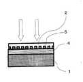
図2以下に具体的なインプリントの工程を示す。図2に示すようにインプリント用のモールドとして石英モールド2を用いた。石英モールド2の作成方法は、先ずインプリントのモールド用の材料として紫外線の透過率の良い石英を用意し、次に石英基板上にレジストを塗布し、通常のフォトリソグラフィーまたは電子線描画によりストライプ状または多角形状のパターンを露光し現像した。次に、Alを100nm程度蒸着し、リフトオフした。さらに、AlをマスクとしてCHF3を用いたRIEで石英を所定の深さまでエッチング加工を行った。加工後に残った不要なAlはリン酸で除去した。最後に純水で洗浄し乾燥させ、石英モールド2を完成させた。 A specific imprint process is shown in FIG. As shown in FIG. 2, a
次に図2のサファイア基板1にスパッター法などでNi層4を積層し、その上に紫外線硬化型のフォトレジスト5を塗布した。 Next, a
次に図3に示すように、石英モールド2をフォトレジスト5に押しつけ、図4のように加圧してフォトレジスト5を変形させ、ストライプ状とした。 Next, as shown in FIG. 3, the
次に図5に示すように、石英モールド2をストライプ状のフォトレジスト5に押しつけたまま、石英モールド2を通して紫外線7を照射してストライプ状のフォトレジスト5を硬化させた。 Next, as shown in FIG. 5, while the
この時紫外線7を照射する方向は石英モールド2側からとしたが、サファイア基板1は透明体であるので、サファイア基板1側から紫外線を照射しても構わない。なお、この場合はモールドの材質は必ずしも透明体である必要はないので、石英以外の材質、例えばシリコンなどの不透明体を用いても構わない。また、透明な材料としてサファイアをモールドに使うことも出来る。また、モールドの形状は通常は二次元のパターンを持つ物を用いるが、必要に応じて三次元のパターン形状を持つ物を作成して用いることも出来る。これにより、サファイア基板を三次元的に加工し、溝の深さを場所によって変えることも出来るの。これによって例えば、当該基板上に作成したLEDから取り出す光の方向を制御することも出来る。 At this time, the direction of irradiating the ultraviolet ray 7 is from the
なお、このインプリントの一連の工程は、フォトレジスト内に気泡が取り込まれないように真空雰囲気中で行った。なお、ここではインプリント法として光ナノインプリント法による例を示したが、この他に熱によってレジストを硬化させる熱ナノインプリント法やSOGを用いて室温で硬化させる室温ナノインプリント法を用いることも出来る。 This series of imprinting steps was performed in a vacuum atmosphere so that bubbles were not taken into the photoresist. In addition, although the example by the optical nanoimprinting method was shown here as an imprinting method, the thermal nanoimprinting method which hardens a resist with a heat | fever, and the room temperature nanoimprinting method hardened at room temperature using SOG can also be used.
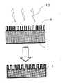
次に図6に示すようにストライプ状のフォトレジスト5を硬化させた後、石英モールド2を引き離し、ストライプ状のフォトレジスト5以外の石英モールド2の凸部に相当する部分のNi層4上に薄く残った不要なフォトレジストを酸素RIEで除去した。 Next, as shown in FIG. 6, after the stripe-shaped
その後、図7に示すようにストライプ状のレジスト5をマスクとしてNi層4をガスプラズマ8によるドライエッチングにより除去し、ストライプ状とし、その後残った不要なレジストを除去した。なお、ストライプ状のNiの形成は、先にレジストを塗布してレジストをインプリント法によりストライプ状とし、その上からNiを積層し、その後不要なNiをレジストごと除去する、いわゆるリフトオフ法で行っても良い。 Thereafter, as shown in FIG. 7, the
次に図8に示すように、このストライプ状のNi層4をマスクとしてサファイア基板3をリアクティブイオン10によりエッチングを行い、ストライプ状の凹凸を形成する。この時RIEには少なくとも塩素、フッ素、硼素、臭素の何れかを含む塩素系のガスまたはこれらの複数のガスの混合ガスを用いた。 Next, as shown in FIG. 8, the sapphire substrate 3 is etched by
最後にNi層4をウェットエッチングにより除去し、図1に示すストライプ状の溝1bを備えた単結晶サファイア基板1を得ることができる。 Finally, the
以上のように本発明の製造方法によれば、ナノインプリント法を用いることにより、ステッパーのような非常に複雑な光学系に較べ、より簡便な設備でしかもコスト的にも安価にサファイア基板上にサブミクロンからミクロンオーダーの凹凸を作製することが出来る。 As described above, according to the manufacturing method of the present invention, by using the nanoimprint method, it is possible to apply the sub-imprint on the sapphire substrate with simpler equipment and at a lower cost than a very complicated optical system such as a stepper. Irregularities on the order of microns to microns can be produced.
このとき作製したストライプ状の溝1bまたは多角形のパターンの繰り返し周期は、その上に形成するGaN系半導体発光素子の発光波長の1/20以上かつ20倍以下、より好ましくは1/10以上かつ10倍以下であることが望ましい。これは、ストライプ状の溝1bまたは多角形のパターンの繰返し周期が発光素子の発光波長に近いことにより、光の回折または散乱の効果が大きくなり、発光素子からの光取り出し効率が高くなるためである。 The repetition period of the stripe-shaped
次に本発明のストライプ状の溝1bまたは多角形のパターンの凹凸を備えたサファイア基板1を用いた半導体発光素子について説明する。 Next, a semiconductor light-emitting element using the
上記ストライプ状の溝1bまたは多角形のパターンの凹凸を備えたサファイア基板の主面1a上に窒化物半導体をエピタキシャル成長させると、窒化物半導体の縦方向の成長と横方向の成長が合体して平坦な表面を有する窒化物半導体膜が形成される。この窒化物半導体を成膜した基板を用いて発光素子を作製する。 When a nitride semiconductor is epitaxially grown on the main surface 1a of the sapphire substrate having the stripe-shaped
この時、ストライプ状の溝1bまたは多角形のパターンの凹凸は窒化物半導体で完全に埋まっていても良く、あるいはストライプ状の溝1bまたは多角形状のパターンの凹凸と窒化物半導体の間に空洞が有っても構わないが、特にLED用途で光り取り出し効率を高める必要がある場合は、好ましくは凹凸が窒化物半導体で完全に埋まっている方が良く、他方、レーザ用途でGaNの結晶性を高める必要がある場合は、好ましくは凹凸と窒化物半導体との間に空洞が有る方が良い。 At this time, the unevenness of the stripe-shaped
このようにして作製されたLEDの例を図9に示す。ストライプ状の溝1bを形成した単結晶サファイア基板1の主面上に、AlGaN低温バッファ層14を介してn型GaNコンタクト層15、n型AlGaNクラッド層16、GaN系半導体発光層(MQW構造)17、p型AlGaNクラッド層18、p型GaNコンタクト層19を形成し、この上に上部電極(通常はp型電極)20を、上記n型GaNコンタクト層15上に下部電極(通常はn型電極)21を形成したものである。 An example of the LED thus manufactured is shown in FIG. An n-type
上記ストライプ状の溝1bまたは多角形状のパターンの凹凸を有する主面1aは光散乱層を形成し、これにより、発光層17から出た光の内、下方に向かう光は主面の光散乱層で散乱され、サファイア基板1から横方向に光を取り出すことが出来る。これにより、発光層17から出た光はGaN層内で反射を繰り返して減衰することが無く、LED全体の光取り出し効率の改善が出来る。なお、このストライプ状の溝1bまたは多角形の凹凸と主面1aのなす角度は10°以上90°未満であることが好ましいが、これは光を効率良く散乱させるためにこの角度が適しているためである。 The stripe-shaped
なお、GaNの結晶成長モードとしては、前記単結晶サファイア基板1の主面1aから、第二の結晶層であるn型GaNコンタクト層15等が実質的にファセット構造を形成しながら成長していることが好ましい。これは、ファセット構造を形成することによりGaN結晶中の転位を横方向に曲げることが出来るので、より結晶性の高いGaN膜を形成する事が出来、LEDの発光効率をより高めることが出来るためである。 As a GaN crystal growth mode, the n-type
また、前記GaN系半導体発光層17から発せられる光の波長における、単結晶サファイア基板1の屈折率と第二の結晶層であるn型GaNコンタクト層15等の屈折率は異なることが好ましく、さらに屈折率の差が0.05以上であることがより好ましい。これは、屈折率に差があり、より好ましくは0.05以上の差があることによって界面での乱反射が起こり易くなり、光取り出し効率が向上するためである。 Moreover, it is preferable that the refractive index of the single
なお、上記バッファ層14としてはAlXGaYN(X+Y=1,X≧0,Y≧0)を含むGaN系またはAlN系のいずれかを用い、その上に形成する半導体結晶層としてはGaN系を用いる。この時、ストライプ状または多角形状の凹凸を持つ単結晶サファイア基板上にGaN膜を成長させる場合にも、バッファ層としてAlXGaYN(X+Y=1,X≧0,Y≧0)を用いることにより、結晶性の良いGaN膜を成長させることが出来る。 As the
さらに他の実施形態として、図示していないが、前記単結晶サファイア基板の主面上に、第一のGaN系半導体結晶がストライプ状の溝を覆って凹凸をなすように成長し、該凹凸の少なくとも一部を覆って、第一のGaN系半導体結晶とは異なる屈折率を有する第二のGaN系半導体結晶が成長し、さらに第三のGaN系半導体結晶が前記凹凸を平坦化するまで成長し、その上に発光層を含む半導体結晶層が積層された素子構造とすることもできる。この様な構造とすることによって、上記凹凸を含む界面からの光の散乱を効率的に起こし、光取り出し効率の高い半導体発光素子を形成することが出来る。 As yet another embodiment, although not shown, the first GaN-based semiconductor crystal is grown on the main surface of the single crystal sapphire substrate so as to cover the stripe-shaped groove so as to form irregularities. A second GaN-based semiconductor crystal having a refractive index different from that of the first GaN-based semiconductor crystal is grown, covering at least a part, and further grown until the third GaN-based semiconductor crystal flattens the unevenness. In addition, an element structure in which a semiconductor crystal layer including a light emitting layer is stacked thereon may be used. With such a structure, it is possible to efficiently cause light scattering from the interface including the above-described irregularities, and to form a semiconductor light emitting device with high light extraction efficiency.
あるいは、単結晶サファイア基板の主面上に、第一のGaN系半導体結晶がストライプ状の溝を覆って凹凸をなすように成長し、該凹凸の少なくとも凸部を膜状に覆って第二のGaN系半導体結晶が成長し、さらにこれを覆って第三のGaN系半導体結晶が前記凹凸を平坦化するまで成長し、その上に発光層を含む半導体結晶層が積層された素子構造を有し、前記第二のGaN系半導体結晶が多層膜構造を有するようにしても良い。この多層膜構造はMWQ構造を含む。このことにより発光効率の高い半導体発光素子を形成することが出来、高い発光効率と高い光取り出し効率の両方を同時に実現できるものである。 Alternatively, the first GaN-based semiconductor crystal is grown on the main surface of the single crystal sapphire substrate so as to cover the stripe-shaped groove so as to form an unevenness, and at least the convex portion of the unevenness is covered in a film shape to form a second A GaN-based semiconductor crystal grows, and further covers a third GaN-based semiconductor crystal until the unevenness is flattened, and a semiconductor crystal layer including a light emitting layer is stacked thereon. The second GaN-based semiconductor crystal may have a multilayer structure. This multilayer film structure includes an MWQ structure. This makes it possible to form a semiconductor light emitting device with high light emission efficiency, and to realize both high light emission efficiency and high light extraction efficiency at the same time.
なお、通常はこの半導体発光素子は上記ストライプ状の溝1bまたは多角形のパターンの凹凸を有するサファイア基板1上に作製され、サファイア基板と共にダイシングなどの切断を行い、パッケージングを行い半導体発光素子としての機能を果たす。しかし、半導体発光素子部分をサファイア基板から剥離してさらに高効率のLEDとする場合もある。その様な場合にも当該ストライプ状の溝または多角形のパターンの凹凸を有するサファイア基板は、ストライプ状の溝または多角形のパターンの凹凸と窒化物半導体膜との間に空洞を有する構造とすることにより、半導体発光素子をサファイア基板から剥離することが容易であるという特徴も有する。 In general, the semiconductor light emitting device is manufactured on the
さらに、本発明のストライプ状の溝または多角形のパターンの凹凸を有するサファイア基板1は、半導体発光素子の製造以外の用途として、当該ストライプ状の溝または多角形のパターンの凹凸を有するサファイア基板上に低転転位の窒化物半導体層を100μm以上の厚さに形成した後、サファイア基板から低転位の窒化物半導体を剥離して独立した窒化物半導体基板を作製する場合にも剥離が容易であるという特徴も有する。 Furthermore, the
さらに、本発明のストライプ状の溝または多角形のパターンの凹凸を有するサファイア基板は、半導体発光素子用の基板としてだけでなく、窒化物半導体を用いた電子デバイス用の基板として用いることも出来る。 Furthermore, the sapphire substrate having striped grooves or polygonal pattern irregularities according to the present invention can be used not only as a substrate for a semiconductor light emitting device but also as a substrate for an electronic device using a nitride semiconductor.
さらに、本発明のストライプ状の溝または多角形のパターンの凹凸を有するサファイア基板は、光学部品として用いることも出来、例えば回折格子やフォトニクス結晶用の部材として用いることも出来る。 Furthermore, the sapphire substrate having striped grooves or polygonal patterns of the present invention can be used as an optical component, for example, a diffraction grating or a member for a photonic crystal.
本実施例では半導体発光素子用のストライプ状の溝または多角形のパターンの凹凸を有するサファイア基板の製造方法を説明する。 In this example, a method for manufacturing a sapphire substrate having stripe-shaped grooves or polygonal pattern irregularities for a semiconductor light emitting device will be described.
初めにEFG法によって面方位、軸方位の定まったサファイア素材を引き上げた。本実施例では特にサファイア基板の主面がC面となるようにしたが、主面の面方位はC面だけでなく、A面、M面、R面、M面から30度回転した面などにも適応できる。また、これらの面から±2°以内でオフアングルしていても良い。 First, a sapphire material with a fixed plane orientation and axial orientation was pulled up by the EFG method. In this embodiment, the main surface of the sapphire substrate is particularly the C plane, but the plane orientation of the main surface is not only the C plane, but also a plane rotated 30 degrees from the A plane, M plane, R plane, M plane, etc. It can also be applied to. Further, it may be off-angled within ± 2 ° from these surfaces.
次に、この素材を適宜切断、研削加工、研磨加工、洗浄を施し、窒化物半導体を成膜するためのサファイア基板を作製した。 Next, this material was appropriately cut, ground, polished, and washed to produce a sapphire substrate for forming a nitride semiconductor.
引き続き、ナノインプリント法により上記サファイア基板上にストライプ状のNiのパターンを形成した。 Subsequently, a striped Ni pattern was formed on the sapphire substrate by nanoimprinting.
ここで、ナノインプリント法についてさらに詳しく説明するが、本実施例では、光インプリントリソグラフィー法に依る場合について述べる。 Here, the nanoimprint method will be described in more detail. In this embodiment, a case of using the optical imprint lithography method will be described.
先ず、インプリント用のモールドとして紫外線の透過率の良い石英を用いた。石英基板上にレジストを塗布し、通常のフォトリソグラフィーによりストライプ状のパターンを露光し、現像した。 First, quartz having a good ultraviolet transmittance was used as an imprint mold. A resist was coated on a quartz substrate, and a stripe pattern was exposed and developed by ordinary photolithography.
次に、Alを100nm程度蒸着し、リフトオフした。さらに、AlをマスクとしてCHF3を用いたRIEで石英を所定の深さまでエッチング加工を行った。加工後に残ったAlはリン酸で除去した。最後に完成した石英モールドを純水で洗浄し乾燥させた。 Next, Al was evaporated to about 100 nm and lifted off. Further, the quartz was etched to a predetermined depth by RIE using CHF3 using Al as a mask. Al remaining after processing was removed with phosphoric acid. Finally, the completed quartz mold was washed with pure water and dried.
次にスパッター法などでNiを積層したサファイア基板に紫外線硬化型のフォトレジストを塗布した後、上記石英モールドをフォトレジストに接触させて加圧し、フォトレジストを変形させ、石英モールドを通して紫外線を照射し、フォトレジストを硬化させた。このインプリントの一連の工程は、フォトレジスト内に気泡が取り込まれないように真空雰囲気中で行った。 Next, after applying an ultraviolet curable photoresist to a sapphire substrate with Ni layer deposited by sputtering, the quartz mold is brought into contact with the photoresist and pressed, the photoresist is deformed, and ultraviolet rays are irradiated through the quartz mold. The photoresist was cured. This series of imprinting steps was performed in a vacuum atmosphere so that bubbles were not taken into the photoresist.
フォトレジストを硬化させた後、石英モールドを引き離し、Niを積層したサファイア基板上の石英モールドの凸部に相当する部分に薄く残った不要なフォトレジストを酸素RIEで除去した。その後、残ったレジスト膜をマスクとしてNiをドライエッチングにより除去し、サファイア基板上にストライプ状のNiのパターンを形成した。 After the photoresist was cured, the quartz mold was pulled away, and unnecessary photoresist remaining thinly on the portion corresponding to the convex portion of the quartz mold on the Ni-laminated sapphire substrate was removed by oxygen RIE. Thereafter, Ni was removed by dry etching using the remaining resist film as a mask, and a striped Ni pattern was formed on the sapphire substrate.
次に、このストライプ状にNiのパターンを形成したサファイア基板をRIE法により、塩素系のガスを用いてドライエッチングすることにより該サファイア基板の主面上に凹凸を形成した。 Next, the sapphire substrate on which the Ni pattern was formed in a stripe shape was dry-etched using a chlorine-based gas by the RIE method to form irregularities on the main surface of the sapphire substrate.
最後にNiをウェットエッチングにより除去し、GaN系半導体発光素子用のサファイア基板を作成した。 Finally, Ni was removed by wet etching to produce a sapphire substrate for a GaN-based semiconductor light emitting device.
本実施例では、ファセット成長法によってサファイア基板のストライプ状の溝または多角形のパターンの凹凸を埋め込んで光散乱面とし、GaN系LEDを製作した。 In this example, a GaN-based LED was manufactured by embedding stripe grooves or polygonal pattern irregularities on a sapphire substrate by a facet growth method to form a light scattering surface.
先ず、実施例1の工程により、C面サファイア基板上にストライプ状の溝または多角形のパターンの凹凸を形成した。当該基板を洗浄後、MOVPE装置に基板を装着し、窒素ガス主成分雰囲気下で1100℃まで昇温し、サーマルクリーニングを行った。温度を500℃まで下げ、周期率表第3族原料としてトリメチルガリウム(以下TMG)を、N原料としてアンモニアを流し、厚さ30nmのAlGaN低温バッファ層を成長させた。 First, according to the process of Example 1, striped grooves or polygonal pattern irregularities were formed on a C-plane sapphire substrate. After cleaning the substrate, the substrate was mounted on a MOVPE apparatus, and the temperature was raised to 1100 ° C. in a nitrogen gas main component atmosphere to perform thermal cleaning. The temperature was lowered to 500 ° C., trimethylgallium (hereinafter referred to as TMG) was flown as a Group 3 raw material of the periodic rate table, and ammonia was flowed as an N raw material to grow an AlGaN low-temperature buffer layer having a thickness of 30 nm.
続いて温度を1000℃に昇温し原料としてTMG、アンモニアを、ドーパントとしてシランを流しn型GaN層(コンタクト層)を成長させた。このときのGaN層の成長は、凸部の上面、凹部の底面から、断面山形でファセット面を含む尾根状の結晶として発生した後、凹部内に空洞を形成することなく、全体を埋め込む成長であった。 Subsequently, the temperature was raised to 1000 ° C., and TMG and ammonia as raw materials and silane as a dopant were flown to grow an n-type GaN layer (contact layer). The growth of the GaN layer at this time is a growth in which the entire surface is formed without forming a cavity in the concave portion after generating from a top surface of the convex portion and a bottom surface of the concave portion as a ridge-like crystal having a mountain-shaped cross section and including a facet surface. there were.
ファセット構造成長において、GaN結晶のC面が完全に消滅し頂部が尖った凸状となった時点で、成長条件を横方向成長が優勢になる条件(成長温度を上昇させるなど)に切り替え、サファイア基板の上面から厚さ5μmまでGaN結晶を成長させた。上面が平坦な埋め込み層を得るためには5μmの厚膜成長が必要であった。 In facet growth, when the C-plane of the GaN crystal is completely extinguished and the top is pointed and convex, the growth conditions are switched to conditions in which lateral growth predominates (e.g., the growth temperature is increased). A GaN crystal was grown from the upper surface of the substrate to a thickness of 5 μm. In order to obtain a buried layer having a flat upper surface, a thick film growth of 5 μm was necessary.
続いて、n型AlGaNクラッド層、InGaN発光層(MQW構造)、p型AlGaNクラッド層、p型GaNコンタクト層を順に形成し、発光波長370nmの紫外線LED用エピ基板とし、さらに、n型コンタクト層を表出させるためのエッチング加工、電極形成、素子分離を行い、LED素子とした。 Subsequently, an n-type AlGaN clad layer, an InGaN light-emitting layer (MQW structure), a p-type AlGaN clad layer, and a p-type GaN contact layer are formed in this order to obtain an epi substrate for an ultraviolet LED having an emission wavelength of 370 nm, and further, an n-type contact layer The LED element was obtained by performing etching processing for exposing the electrode, electrode formation, and element separation.
本発明は、半導体発光素子用単結晶サファイア基板とその製造方法及び半導体発光素子に関する物であり、半導体発光素子用サファイア基板を簡易な設備で安価に製造することに寄与することが出来るものである。 The present invention relates to a single crystal sapphire substrate for a semiconductor light emitting device, a manufacturing method thereof, and a semiconductor light emitting device, and can contribute to manufacturing a sapphire substrate for a semiconductor light emitting device at low cost with simple equipment. .
1:単結晶サファイア基板
1a:主面
1b:溝
2:石英モールド
4:ニッケル層
5:フォトレジスト
7:紫外線
8:ガスプラズマ
10:リアクティブイオン
14:AlGaN低温バッファ層
15:n型GaNコンタクト層
16:n型AlGaNクラッド層
17:GaN系半導体発光層(MQW構造)
18:p型AlGaNクラッド層
19:p型GaNコンタクト層
20:上部電極
21:下部電極1: Single crystal sapphire substrate 1a:
18: p-type AlGaN cladding layer 19: p-type GaN contact layer 20: upper electrode 21: lower electrode
Claims (24)
Translated fromJapanesePriority Applications (1)
| Application Number | Priority Date | Filing Date | Title |
|---|---|---|---|
| JP2003369679AJP2005136106A (en) | 2003-10-29 | 2003-10-29 | Single crystal sapphire substrate, manufacturing method thereof, and semiconductor light emitting device |
Applications Claiming Priority (1)
| Application Number | Priority Date | Filing Date | Title |
|---|---|---|---|
| JP2003369679AJP2005136106A (en) | 2003-10-29 | 2003-10-29 | Single crystal sapphire substrate, manufacturing method thereof, and semiconductor light emitting device |
Publications (1)
| Publication Number | Publication Date |
|---|---|
| JP2005136106Atrue JP2005136106A (en) | 2005-05-26 |
Family
ID=34646924
Family Applications (1)
| Application Number | Title | Priority Date | Filing Date |
|---|---|---|---|
| JP2003369679APendingJP2005136106A (en) | 2003-10-29 | 2003-10-29 | Single crystal sapphire substrate, manufacturing method thereof, and semiconductor light emitting device |
Country Status (1)
| Country | Link |
|---|---|
| JP (1) | JP2005136106A (en) |
Cited By (38)
| Publication number | Priority date | Publication date | Assignee | Title |
|---|---|---|---|---|
| JP2007072374A (en)* | 2005-09-09 | 2007-03-22 | Tokyo Ohka Kogyo Co Ltd | Film forming composition for nanoimprint and pattern forming method |
| JP2007088277A (en)* | 2005-09-22 | 2007-04-05 | Matsushita Electric Works Ltd | Semiconductor light-emitting element and manufacturing method thereof |
| JP2007088273A (en)* | 2005-09-22 | 2007-04-05 | Matsushita Electric Works Ltd | Semiconductor light-emitting element and manufacturing method thereof |
| JP2007101799A (en)* | 2005-10-03 | 2007-04-19 | Nippon Sheet Glass Co Ltd | Transmission optical element |
| JP2007150053A (en)* | 2005-11-29 | 2007-06-14 | Kyocera Corp | Optical imprint stamper and light emitting device manufacturing method using the same |
| JP2007194550A (en)* | 2006-01-23 | 2007-08-02 | Toppan Printing Co Ltd | Imprint mold and manufacturing method thereof |
| JP2007227890A (en)* | 2005-12-21 | 2007-09-06 | Asml Netherlands Bv | Imprint lithography |
| JP2007287951A (en)* | 2006-04-18 | 2007-11-01 | Canon Inc | Substrate processing method and method for manufacturing member having pattern region |
| WO2008114685A1 (en)* | 2007-03-14 | 2008-09-25 | Omron Corporation | Method for manufacturing solar cell and solar cell |
| JP2009009978A (en)* | 2007-06-26 | 2009-01-15 | Panasonic Electric Works Co Ltd | COMPOUND SEMICONDUCTOR ELEMENT, LIGHTING DEVICE USING SAME, AND METHOD FOR PRODUCING COMPOUND SEMICONDUCTOR ELEMENT |
| JP2009054882A (en)* | 2007-08-28 | 2009-03-12 | Univ Of Tokushima | Method for manufacturing light emitting device |
| JP2009226660A (en)* | 2008-03-21 | 2009-10-08 | Fujifilm Corp | Method for patterning by dry etching, mold used for it and method for manufacturing inkjet head |
| EP2136390A2 (en) | 2008-06-19 | 2009-12-23 | Nanogan Limited | Production of semiconductor material and devices using oblique angle etched templates |
| KR100957570B1 (en) | 2008-07-25 | 2010-05-11 | 이헌 | Manufacturing method of high efficiency light emitting diode substrate |
| US7781790B2 (en) | 2006-12-21 | 2010-08-24 | Nichia Corporation | Method for manufacturing substrate for semiconductor light emitting element and semiconductor light emitting element using the same |
| JP2010263236A (en)* | 2006-12-22 | 2010-11-18 | Showa Denko Kk | Group III nitride semiconductor light emitting device manufacturing method |
| WO2011021753A1 (en)* | 2009-08-18 | 2011-02-24 | 우리엘에스티 주식회사 | Group iii-nitride semiconductor light emitting device and fabrication method thereof |
| US8118934B2 (en) | 2007-09-26 | 2012-02-21 | Wang Nang Wang | Non-polar III-V nitride material and production method |
| JP2013058767A (en)* | 2012-10-19 | 2013-03-28 | Dainippon Printing Co Ltd | Method for forming pattern and method for manufacturing template |
| US8652947B2 (en) | 2007-09-26 | 2014-02-18 | Wang Nang Wang | Non-polar III-V nitride semiconductor and growth method |
| JP2014078653A (en)* | 2012-10-12 | 2014-05-01 | Waseda Univ | Group iii nitride semiconductor layer manufacturing method |
| US8828849B2 (en) | 2007-01-19 | 2014-09-09 | Nanogan Limited | Production of single-crystal semiconductor material using a nanostructure template |
| JP2014197693A (en)* | 2014-05-29 | 2014-10-16 | 大日本印刷株式会社 | Method of forming pattern and process of manufacturing template |
| JP2015076512A (en)* | 2013-10-09 | 2015-04-20 | 株式会社トクヤマ | Pattern formation method |
| JP2015515145A (en)* | 2012-04-18 | 2015-05-21 | ヒューネット プラス カンパニー リミテッドHunet Plus Co., Ltd. | Method of manufacturing a substrate for a high-efficiency nitride-based light-emitting diode having a nano-level pattern (MethodFor Fabricating NanoPatternedSubstituteForHighEfficiencyNitridebasedLightEmittingDiode) |
| US9154678B2 (en) | 2013-12-11 | 2015-10-06 | Apple Inc. | Cover glass arrangement for an electronic device |
| KR20150119180A (en)* | 2013-02-11 | 2015-10-23 | 코닌클리케 필립스 엔.브이. | A light emitting device and method for manufacturing a light emitting device |
| US9221289B2 (en) | 2012-07-27 | 2015-12-29 | Apple Inc. | Sapphire window |
| US9225056B2 (en) | 2014-02-12 | 2015-12-29 | Apple Inc. | Antenna on sapphire structure |
| US9232672B2 (en) | 2013-01-10 | 2016-01-05 | Apple Inc. | Ceramic insert control mechanism |
| JP2016027658A (en)* | 2015-09-07 | 2016-02-18 | エルシード株式会社 | Etching method |
| JP2016155962A (en)* | 2015-02-25 | 2016-09-01 | 株式会社Flosfia | Production process for fluophor composition and light-emitting device |
| US9472736B2 (en) | 2011-11-15 | 2016-10-18 | El-Seed Corporation | Etching method |
| JP2017063099A (en)* | 2015-09-24 | 2017-03-30 | 国立研究開発法人情報通信研究機構 | Manufacturing method of substrate including uneven structure and manufacturing method of semiconductor light emitting device |
| US9632537B2 (en) | 2013-09-23 | 2017-04-25 | Apple Inc. | Electronic component embedded in ceramic material |
| US9678540B2 (en) | 2013-09-23 | 2017-06-13 | Apple Inc. | Electronic component embedded in ceramic material |
| US10052848B2 (en) | 2012-03-06 | 2018-08-21 | Apple Inc. | Sapphire laminates |
| US10406634B2 (en) | 2015-07-01 | 2019-09-10 | Apple Inc. | Enhancing strength in laser cutting of ceramic components |
- 2003
- 2003-10-29JPJP2003369679Apatent/JP2005136106A/enactivePending
Cited By (48)
| Publication number | Priority date | Publication date | Assignee | Title |
|---|---|---|---|---|
| JP2007072374A (en)* | 2005-09-09 | 2007-03-22 | Tokyo Ohka Kogyo Co Ltd | Film forming composition for nanoimprint and pattern forming method |
| JP2007088277A (en)* | 2005-09-22 | 2007-04-05 | Matsushita Electric Works Ltd | Semiconductor light-emitting element and manufacturing method thereof |
| JP2007088273A (en)* | 2005-09-22 | 2007-04-05 | Matsushita Electric Works Ltd | Semiconductor light-emitting element and manufacturing method thereof |
| JP2007101799A (en)* | 2005-10-03 | 2007-04-19 | Nippon Sheet Glass Co Ltd | Transmission optical element |
| JP2007150053A (en)* | 2005-11-29 | 2007-06-14 | Kyocera Corp | Optical imprint stamper and light emitting device manufacturing method using the same |
| JP2007227890A (en)* | 2005-12-21 | 2007-09-06 | Asml Netherlands Bv | Imprint lithography |
| JP2007194550A (en)* | 2006-01-23 | 2007-08-02 | Toppan Printing Co Ltd | Imprint mold and manufacturing method thereof |
| JP2007287951A (en)* | 2006-04-18 | 2007-11-01 | Canon Inc | Substrate processing method and method for manufacturing member having pattern region |
| US7781790B2 (en) | 2006-12-21 | 2010-08-24 | Nichia Corporation | Method for manufacturing substrate for semiconductor light emitting element and semiconductor light emitting element using the same |
| US8686457B2 (en) | 2006-12-21 | 2014-04-01 | Nichia Corporation | Method for manufacturing substrate for semiconductor light emitting element and semiconductor light emitting element using the same |
| US9054271B2 (en) | 2006-12-21 | 2015-06-09 | Nichia Corporation | Method for manufacturing substrate for semiconductor light emitting element and semiconductor light emitting element using the same |
| US8394652B2 (en) | 2006-12-21 | 2013-03-12 | Nichia Corporation | Method for manufacturing substrate for semiconductor light emitting element and semiconductor light emitting element using the same |
| US8492186B2 (en) | 2006-12-22 | 2013-07-23 | Toyoda Gosei Co., Ltd. | Method for producing group III nitride semiconductor layer, group III nitride semiconductor light-emitting device, and lamp |
| JP2010263236A (en)* | 2006-12-22 | 2010-11-18 | Showa Denko Kk | Group III nitride semiconductor light emitting device manufacturing method |
| US8828849B2 (en) | 2007-01-19 | 2014-09-09 | Nanogan Limited | Production of single-crystal semiconductor material using a nanostructure template |
| JPWO2008114685A1 (en)* | 2007-03-14 | 2010-07-01 | オムロン株式会社 | Method for manufacturing solar cell and solar cell |
| WO2008114685A1 (en)* | 2007-03-14 | 2008-09-25 | Omron Corporation | Method for manufacturing solar cell and solar cell |
| JP2009009978A (en)* | 2007-06-26 | 2009-01-15 | Panasonic Electric Works Co Ltd | COMPOUND SEMICONDUCTOR ELEMENT, LIGHTING DEVICE USING SAME, AND METHOD FOR PRODUCING COMPOUND SEMICONDUCTOR ELEMENT |
| JP2009054882A (en)* | 2007-08-28 | 2009-03-12 | Univ Of Tokushima | Method for manufacturing light emitting device |
| US8652947B2 (en) | 2007-09-26 | 2014-02-18 | Wang Nang Wang | Non-polar III-V nitride semiconductor and growth method |
| US8118934B2 (en) | 2007-09-26 | 2012-02-21 | Wang Nang Wang | Non-polar III-V nitride material and production method |
| JP2009226660A (en)* | 2008-03-21 | 2009-10-08 | Fujifilm Corp | Method for patterning by dry etching, mold used for it and method for manufacturing inkjet head |
| EP2136390A2 (en) | 2008-06-19 | 2009-12-23 | Nanogan Limited | Production of semiconductor material and devices using oblique angle etched templates |
| KR100957570B1 (en) | 2008-07-25 | 2010-05-11 | 이헌 | Manufacturing method of high efficiency light emitting diode substrate |
| WO2011021753A1 (en)* | 2009-08-18 | 2011-02-24 | 우리엘에스티 주식회사 | Group iii-nitride semiconductor light emitting device and fabrication method thereof |
| US9472736B2 (en) | 2011-11-15 | 2016-10-18 | El-Seed Corporation | Etching method |
| US10052848B2 (en) | 2012-03-06 | 2018-08-21 | Apple Inc. | Sapphire laminates |
| JP2015515145A (en)* | 2012-04-18 | 2015-05-21 | ヒューネット プラス カンパニー リミテッドHunet Plus Co., Ltd. | Method of manufacturing a substrate for a high-efficiency nitride-based light-emitting diode having a nano-level pattern (MethodFor Fabricating NanoPatternedSubstituteForHighEfficiencyNitridebasedLightEmittingDiode) |
| US9221289B2 (en) | 2012-07-27 | 2015-12-29 | Apple Inc. | Sapphire window |
| JP2014078653A (en)* | 2012-10-12 | 2014-05-01 | Waseda Univ | Group iii nitride semiconductor layer manufacturing method |
| JP2013058767A (en)* | 2012-10-19 | 2013-03-28 | Dainippon Printing Co Ltd | Method for forming pattern and method for manufacturing template |
| US9232672B2 (en) | 2013-01-10 | 2016-01-05 | Apple Inc. | Ceramic insert control mechanism |
| KR20150119180A (en)* | 2013-02-11 | 2015-10-23 | 코닌클리케 필립스 엔.브이. | A light emitting device and method for manufacturing a light emitting device |
| KR102120264B1 (en)* | 2013-02-11 | 2020-06-09 | 루미리즈 홀딩 비.브이. | A light emitting device and method for manufacturing a light emitting device |
| US9632537B2 (en) | 2013-09-23 | 2017-04-25 | Apple Inc. | Electronic component embedded in ceramic material |
| US9678540B2 (en) | 2013-09-23 | 2017-06-13 | Apple Inc. | Electronic component embedded in ceramic material |
| JP2015076512A (en)* | 2013-10-09 | 2015-04-20 | 株式会社トクヤマ | Pattern formation method |
| US10386889B2 (en) | 2013-12-11 | 2019-08-20 | Apple Inc. | Cover glass for an electronic device |
| US10324496B2 (en) | 2013-12-11 | 2019-06-18 | Apple Inc. | Cover glass arrangement for an electronic device |
| US9154678B2 (en) | 2013-12-11 | 2015-10-06 | Apple Inc. | Cover glass arrangement for an electronic device |
| US9692113B2 (en) | 2014-02-12 | 2017-06-27 | Apple Inc. | Antenna on sapphire structure |
| US9461357B2 (en) | 2014-02-12 | 2016-10-04 | Apple Inc. | Antenna on sapphire structure |
| US9225056B2 (en) | 2014-02-12 | 2015-12-29 | Apple Inc. | Antenna on sapphire structure |
| JP2014197693A (en)* | 2014-05-29 | 2014-10-16 | 大日本印刷株式会社 | Method of forming pattern and process of manufacturing template |
| JP2016155962A (en)* | 2015-02-25 | 2016-09-01 | 株式会社Flosfia | Production process for fluophor composition and light-emitting device |
| US10406634B2 (en) | 2015-07-01 | 2019-09-10 | Apple Inc. | Enhancing strength in laser cutting of ceramic components |
| JP2016027658A (en)* | 2015-09-07 | 2016-02-18 | エルシード株式会社 | Etching method |
| JP2017063099A (en)* | 2015-09-24 | 2017-03-30 | 国立研究開発法人情報通信研究機構 | Manufacturing method of substrate including uneven structure and manufacturing method of semiconductor light emitting device |
Similar Documents
| Publication | Publication Date | Title |
|---|---|---|
| JP2005136106A (en) | Single crystal sapphire substrate, manufacturing method thereof, and semiconductor light emitting device | |
| KR101897481B1 (en) | Solid state light emitting devices based on crystallographically relaxed structures | |
| JP2005064492A (en) | Single crystal sapphire substrate, manufacturing method thereof, and semiconductor light emitting device | |
| US7122827B2 (en) | Monolithic light emitting devices based on wide bandgap semiconductor nanostructures and methods for making same | |
| JP4471726B2 (en) | Method for producing single crystal sapphire substrate | |
| JP5666164B2 (en) | Method for manufacturing light emitting device | |
| JP4939099B2 (en) | Method for manufacturing vertical structure group 3 nitride light emitting device | |
| JP3471685B2 (en) | Semiconductor substrate and manufacturing method thereof | |
| JP4593890B2 (en) | Manufacturing method of semiconductor light emitting device | |
| US10622515B2 (en) | Patterned layer design for group III nitride layer growth | |
| JP5306779B2 (en) | Light emitting device and manufacturing method thereof | |
| CN101290908A (en) | Method for obtaining high quality margins of semiconductor devices fabricated on segmented substrates | |
| US20150221824A1 (en) | Substrate for semiconductor light emitting device and semiconductor light emitting device, and manufacturing methods thereof | |
| US9355840B2 (en) | High quality devices growth on pixelated patterned templates | |
| TWI491072B (en) | Pattern layer design for the growth of Group III nitride layers | |
| CN104393127B (en) | Inversion light emitting diode (LED) and production method thereof | |
| CN104157759A (en) | High density and high uniformity InGaN quantum dot structure and growth method thereof | |
| JP6429626B2 (en) | Design of substrates with patterns for layer growth | |
| TW201904086A (en) | Light-emitting diode | |
| JP3471687B2 (en) | Semiconductor substrate and manufacturing method thereof | |
| JP2009043895A (en) | Light emitting element | |
| CN102969339A (en) | Nitride semiconductor substrate and manufacturing method thereof | |
| JP2009176805A (en) | Surface roughening method for light emitting diode substrate | |
| TW200820456A (en) | Light emitting diode device and fabrication method thereof | |
| CN115863505A (en) | Nitride light-emitting diode with three-dimensional structure and preparation method thereof |
Legal Events
| Date | Code | Title | Description |
|---|---|---|---|
| A621 | Written request for application examination | Free format text:JAPANESE INTERMEDIATE CODE: A621 Effective date:20061012 | |
| A977 | Report on retrieval | Free format text:JAPANESE INTERMEDIATE CODE: A971007 Effective date:20090424 | |
| A131 | Notification of reasons for refusal | Free format text:JAPANESE INTERMEDIATE CODE: A131 Effective date:20090512 | |
| A521 | Written amendment | Free format text:JAPANESE INTERMEDIATE CODE: A523 Effective date:20090707 | |
| A02 | Decision of refusal | Free format text:JAPANESE INTERMEDIATE CODE: A02 Effective date:20100202 |