JP2005135844A - Optical element and backlight device - Google Patents
Optical element and backlight deviceDownload PDFInfo
- Publication number
- JP2005135844A JP2005135844AJP2003372753AJP2003372753AJP2005135844AJP 2005135844 AJP2005135844 AJP 2005135844AJP 2003372753 AJP2003372753 AJP 2003372753AJP 2003372753 AJP2003372753 AJP 2003372753AJP 2005135844 AJP2005135844 AJP 2005135844A
- Authority
- JP
- Japan
- Prior art keywords
- light
- guide plate
- incident
- light guide
- optical element
- Prior art date
- Legal status (The legal status is an assumption and is not a legal conclusion. Google has not performed a legal analysis and makes no representation as to the accuracy of the status listed.)
- Pending
Links
- 230000003287optical effectEffects0.000titleclaimsabstractdescription77
- 238000009792diffusion processMethods0.000claimsdescription18
- 238000013459approachMethods0.000claimsdescription2
- 238000013461designMethods0.000description12
- 239000004973liquid crystal related substanceSubstances0.000description6
- 229920000178Acrylic resinPolymers0.000description4
- 239000004925Acrylic resinSubstances0.000description4
- 238000001746injection mouldingMethods0.000description4
- 239000000463materialSubstances0.000description4
- 238000004088simulationMethods0.000description4
- 230000000694effectsEffects0.000description3
- 238000012545processingMethods0.000description3
- PPBRXRYQALVLMV-UHFFFAOYSA-NStyreneChemical compoundC=CC1=CC=CC=C1PPBRXRYQALVLMV-UHFFFAOYSA-N0.000description2
- 239000011347resinSubstances0.000description2
- 229920005989resinPolymers0.000description2
- 238000007796conventional methodMethods0.000description1
- 230000007423decreaseEffects0.000description1
- 238000010586diagramMethods0.000description1
- 238000005286illuminationMethods0.000description1
- 238000002347injectionMethods0.000description1
- 239000007924injectionSubstances0.000description1
- 239000000113methacrylic resinSubstances0.000description1
- 229920005668polycarbonate resinPolymers0.000description1
- 239000004431polycarbonate resinSubstances0.000description1
- 230000000630rising effectEffects0.000description1
- 239000000758substrateSubstances0.000description1
- 229920006352transparent thermoplasticPolymers0.000description1
Images


Landscapes
- Planar Illumination Modules (AREA)
- Light Guides In General And Applications Therefor (AREA)
- Liquid Crystal (AREA)
Abstract
Description
Translated fromJapanese本発明は、液晶表示装置(LCD:Liquid Crystal Display)のバックライト装置に関し、詳しくは、バックライト装置の部品点数を大幅に削減するために用いる光学素子及び上記光学素子を備えたバックライト装置に関する。 The present invention relates to a backlight device of a liquid crystal display (LCD), and more particularly, to an optical element used for significantly reducing the number of parts of the backlight device and a backlight device including the optical element. .
液晶表示装置のバックライト装置であるバックライトユニットは、液晶表示装置を搭載する電子機器の普及に伴い、大量生産されることが求められている。バックライトユニットは、主に、光源と、光源から出射された光を導光して面発光させる導光板とによって形成されている。 A backlight unit, which is a backlight device of a liquid crystal display device, is required to be mass-produced with the spread of electronic devices equipped with the liquid crystal display device. The backlight unit is mainly formed by a light source and a light guide plate that guides light emitted from the light source to emit light.
光源は、蛍光管や、発光ダイオード(LED:Light Emitting Diode)などが用いられ、特に小型化、薄型化された電子機器に搭載する場合は、発光ダイオードが使用されることが多い。 As the light source, a fluorescent tube, a light emitting diode (LED), or the like is used. In particular, a light emitting diode is often used when the light source is mounted on a miniaturized and thin electronic device.
一般に、図15に示すように発光ダイオードを光源とするバックライトユニット100は、導光板80、例えば、3個の発光ダイオード91a,91b,91cといった複数の発光ダイオードを有する光源90、反射シート101、拡散シート102、第1のレンズシート103、第2のレンズシート104を備えている。 In general, as shown in FIG. 15, a
バックライトユニット100は、導光板80の光入射面81に、発光ダイオード91a、91b、91cが所定のピッチで、光出射面92a、92b、92cが密着するように配置され、導光板80の光反射面82側に反射シート101が配置され、導光板80の光出射面83上に拡散シート102、第1のレンズシート103、第2のレンズシート104の順に重ねて配置され、これらがフレーム110、111内に、反射シート101をフレーム内面111A側にして、収納され組み付けられて構成されている。なお、以下の説明において、発光ダイオード91a,91b,91cは、総称して発光ダイオード91とも呼ぶ。 The
発光ダイオード91から導光板80の光入射面81に入射した光は、導光板80の光反射面82と、光出射面83との内面で全反射しながら導光される。導光板80の光反射面82には、入射された光を効率よく光出射面83方向へ立ち上げるためのプリズムパターンや、ドットパターンなどが形成されており、これらのパターンによって臨界角以内で光出射面83の内面に入射した光は、光出射面83から出射されることになる。 Light that has entered the
光出射面83から出射した光は、面内光量分布に非常にばらつきがあるため、拡散シート102に入射し均一化が計られる。 Since the light emitted from the
拡散シート102から出射された光は、第1のレンズシート103,第2のレンズシート104に入射され、光出射面83の法線方向へ集光するように偏向させる。拡散シート102を通過した光を、第1のレンズシート103、第2のレンズシート104が集光させる光の方向成分はそれぞれ異なっている。 The light emitted from the
一方の第1のレンズシート103は、Y方向レンズシートとも呼ばれ、図16に、発光ダイオード91を備えた導光板80を、光出射面83が正面となるように、XY座標平面上に配置させ、光の導光方向をX軸方向とした場合のY軸方向の光の成分を、光出射面83の法線方向に集光させるレンズシートである。他方の第2のレンズシート104は、X方向レンズシートともよばれ、図16に示すX軸方向の光の成分を、光出射面83の法線方向に集光させるレンズシートである。 One first lens sheet 103 is also called a Y-direction lens sheet. In FIG. 16, the
このように、導光板80の光出射面83から出射され、拡散シート102を介した光を、この第1のレンズシート103、第2のレンズシート104に通過させることで、バックライトユニット100の正面輝度を効率よく向上させることが可能となる。 In this way, the light emitted from the
なお、導光板80の光反射面82側に配置された反射シート101は、光入射面81から入射された光が導光板80内を全反射しながら導光する際に、光反射面82外に飛び出した光を反射して、再び導光板80内に戻す働きをしている。 The
電子機器の小型化及び薄型化の要請に伴い、このような電子機器に搭載する、例えば、液晶表示装置の照明に用いられるバックライトユニットも薄型化される傾向にある。しかしながら、図15を用いて説明したようにバックライトユニット100の部品点数は、非常に多く、中でも反射シート101、拡散シート102、第1のレンズシート103、第2のレンズシート104というようにシート類が4枚も使用されているという状況である。 With the demand for downsizing and thinning electronic devices, backlight units mounted on such electronic devices, for example, used for illumination of liquid crystal display devices tend to be thinned. However, as described with reference to FIG. 15, the number of parts of the
これらのシート類は、それぞれ0.1〜0.15mm程度の厚さがあるため、重ね合わせると少なくとも0.4mm以上となってしまい、バックライトユニット100の薄型化を妨げてしまうといった問題がある。 Since these sheets each have a thickness of about 0.1 to 0.15 mm, they are at least 0.4 mm or more when they are overlapped, and there is a problem that the
しかしながら、上述した、いずれのシート類が有する機能も、このように光源90から導光板80の光入射面81に入射された光を導光しながら、光出射面83から面発光させる機構のバックライトユニット100においては、いずれも必須であり欠くことのできないものである。 However, the functions of any of the above-described sheets are back of the mechanism for emitting light from the
特に、導光板80の光出射面83上に積層する拡散シート102、第1のレンズシート103、第2のレンズシート104は、正面輝度の劇的な改善効果を期待できる反面、非常に高価な部材である。 In particular, the
具体的には、拡散シート102、第1のレンズシート103及び第2のレンズシート104をバックライトユニット100に組み込んだ場合、この3枚のシートによって、バックライトユニット100の総コストの何割かを占めてしまうことになり、高い正面輝度が必要な場合には、必然的にコストアップが求められてしまうといった問題がある。 Specifically, when the
そこで、本発明はこのような問題を解決するために案出されたものであり、バックライト装置を構成するシート類のうち拡散シート、第1の反射シート、第2の反射シートを、当該拡散シート、第1の反射シート、第2の反射シートの有する機能を損なうことなく削減するための光学素子及び上記光学素子を備えたバックライト装置を提供することを目的とする。 Therefore, the present invention has been devised to solve such a problem, and among the sheets constituting the backlight device, the diffusion sheet, the first reflection sheet, and the second reflection sheet are used as the diffusion sheet. An object of the present invention is to provide an optical element for reducing the function of the sheet, the first reflective sheet, and the second reflective sheet without impairing the function, and a backlight device including the optical element.
上述の目的を達成するために、本発明に係る光学素子は、一側面を光入射面とし、上記光入射面から入射された光を一方主面である光出射面及び他方主面である光反射面とで全反射して導光し、上記光出射面から面発光させる導光板の上記光入射面に入射する光を調整する光学素子であって、光源より出射される光を入射し、入射された光のうち、上記導光板の光の導光方向に対して、放射状に広がって進む指向性を有する光を、上記導光板の上記光の導光方向と平行な方向へと進む指向性を有する光に偏向して、出射し、上記導光板の上記光入射面に入射させる光学手段を備えることを特徴とする。 In order to achieve the above-mentioned object, an optical element according to the present invention has one side as a light incident surface, and light incident from the light incident surface is a light exit surface that is one main surface and light that is the other main surface. It is an optical element that adjusts the light incident on the light incident surface of the light guide plate that is totally reflected by the reflecting surface and guided by light, and emits light from the light emitting surface, and receives the light emitted from the light source, Of the incident light, the light having directivity that spreads radially with respect to the light guide direction of the light of the light guide plate proceeds in a direction parallel to the light guide direction of the light of the light guide plate. And an optical means for deflecting and emitting the light having a property to enter the light incident surface of the light guide plate.
上述の目的を達成するために、本発明に係るバックライト装置は、一側面を光入射面とし、上記光入射面から入射された光を一方主面である光出射面及び他方主面である光反射面とで全反射して導光し、上記光出射面から面発光させる導光板と、上記導光板の上記光入射面の長手方向に所定の間隔で配列された複数の発光素子を有する光源と、上記光源の上記複数の発光素子より出射された光を入射し、上記導光板の上記光入射面への入射光として出射する光学素子と、上記導光板の上記光反射面側に配置される反射シートと、上記導光板に、上記光源と、上記光学素子と、上記反射シートとを保持するフレームとを備え、上記導光板は、上記光の入射方向をX軸方向とし、上記X軸方向に直交し、上記光出射面に平行な方向をY軸方向とし、上記X軸方向及び上記Y軸方向に垂直な方向を法線方向とするとき、上記光入射面から入射された光を、上記X軸方向の傾きが上記法線方向に対してゼロに近付くように偏向して、上記光出射面から出射させる配光制御をするX軸方向配光制御手段を有し、上記光学素子は、上記入射された光のうち、上記導光板の光の導光方向に対して、放射状に広がって進む指向性を有する光を、上記導光板の上記光の導光方向と平行な方向へと進む指向性を有する光に偏向して、出射し、上記導光板の上記光入射面に入射させる光学手段を有することを特徴とする。 In order to achieve the above-described object, a backlight device according to the present invention has one side as a light incident surface, and light incident from the light incident surface is a light exit surface that is one main surface and the other main surface. A light guide plate that is totally reflected by the light reflecting surface and guides light from the light emitting surface, and a plurality of light emitting elements arranged at predetermined intervals in the longitudinal direction of the light incident surface of the light guide plate. A light source, an optical element that receives light emitted from the plurality of light emitting elements of the light source, and is emitted as incident light on the light incident surface of the light guide plate, and disposed on the light reflecting surface side of the light guide plate The light guide plate includes the light source, the optical element, and a frame that holds the reflection sheet. The light guide plate has an X-axis direction as the light incident direction, and the X The direction perpendicular to the axial direction and parallel to the light exit surface is the Y-axis direction. When the normal direction is the direction perpendicular to the X-axis direction and the Y-axis direction, the light incident from the light incident surface is such that the inclination in the X-axis direction approaches zero with respect to the normal direction. The X-axis direction light distribution control means for controlling the light distribution to be emitted from the light exit surface, and the optical element is a light guide direction of the light of the light guide plate out of the incident light. In contrast, light having directivity that spreads radially is deflected to light having directivity that travels in a direction parallel to the light guide direction of the light of the light guide plate, and is emitted. It has an optical means for making it incident on the light incident surface.
本発明の光学素子は、導光板に入射させる光源からの光を、導光板の光の導光方向に対して、放射状に広がって進む指向性を有する光から、導光板の光の導光方向と平行な方向へと進む指向性を有する光に偏向して、出射し、導光板の上記光入射面に入射させる。 The optical element of the present invention is a light guide direction of light of a light guide plate from light having directivity that spreads light from a light source incident on the light guide plate in a radial direction with respect to the light guide direction of light of the light guide plate. The light is deflected to emit light having directivity that travels in a direction parallel to the light, and is incident on the light incident surface of the light guide plate.
これにより、点光源である光源から出射される光を、導光板の光入射面、全面に渡って、垂直に入射させることができるため、導光板から一定レベルの輝度以上で均一な面発光をさせることを可能とする。 As a result, light emitted from the light source, which is a point light source, can be vertically incident on the entire light incident surface of the light guide plate, so that uniform light emission from the light guide plate with a certain level of brightness or more can be achieved. It is possible to make it.
また、本発明のバックライト装置は、上記光学素子によって、導光板の光の導光方向に平行な方向へと進む指向性を有する光に偏向された光を、X軸方向配光制御手段を有する導光板に入射させることで、導光板の光出射面から出射した光に対して、Y軸方向の配光制御、X軸方向の配光制御、光の拡散処理が不要となるためX軸方向の配光制御及びY軸方向の配光制御を行うレンズシート、拡散シートを用いなくとも、一定レベルの輝度以上で均一な面発光を可能とする。 Further, the backlight device of the present invention provides the X-axis direction light distribution control means for converting the light deflected by the optical element into light having directivity that travels in a direction parallel to the light guide direction of the light from the light guide plate. By making the light incident on the light guide plate having the X-axis because light distribution control in the Y-axis direction, light distribution control in the X-axis direction, and light diffusion processing are not required for the light emitted from the light exit surface of the light guide plate Even without using a lens sheet or a diffusion sheet that performs light distribution control in the direction and light distribution control in the Y-axis direction, uniform surface light emission at a certain level or higher is possible.
したがって、このようなバックライト装置は、従来では必須となっていた高額なレンズシート、拡散シートを削減できるため、装置の薄型化及び大幅なコストダウンを可能とする。 Therefore, since such a backlight device can reduce expensive lens sheets and diffusion sheets that have been essential in the past, the device can be thinned and the cost can be significantly reduced.
以下、本発明に係る光学素子及びバックライト装置の発明を実施するための最良の形態を図面を参照して詳細に説明する。 The best mode for carrying out the invention of an optical element and a backlight device according to the present invention will be described below in detail with reference to the drawings.
図1に、本発明を実施するための最良の形態として示すバックライトユニット40を示す。バックライトユニット40は、導光板10と、光源部20と、光学素子30と、反射シート15とが、フレーム35,36内に組み付けられて構成されている。 FIG. 1 shows a
導光板10に用いられる材料としては、アクリル樹脂の他、メタクリル樹脂、スチレン樹脂、ポリカーボネート樹脂等の透明熱可塑性樹脂が用いられる。導光板10は、一例として、透明度の高いアクリル樹脂などを材料とし射出成形される。導光板10は、光入射面11から入射された光を、当該導光板10の一方主面である光反射面12で多方向へ反射させ、反射された光を光出射面13から均一な光として出射させる。 As a material used for the
光反射面12には、細かい凹凸形状、例えば、プリズムパターンや、ドットパターンなどが形成されており、入射され当該導光板10内に導光された光を効率よく光出射面13方向へ立ち上げるような処理が施されている。 The
例えば、光反射面12には、n(nは、自然数)個のプリズム12Anからなるプリズムパターンが形成されており、入射され当該導光板10内に導光された光を効率よく光出射面13方向へ立ち上げる。この光反射面12に形成するプリズムパターンは、導光板10の射出成形時に形成したり、射出成形後に直接加工(ダイレクト・カット)して形成したりする。なお、このプリズムパターン12Anについては、後で詳細に説明をする。 For example, the
導光板10は、光入射面11から入射され、導光された光の導光方向の厚みが徐々に減少するような楔形形状をしているが、本発明は、このような楔形形状以外の形状の導光板にも適用可能である。 The
導光板10の光源としては、図1に示す基板23に所定の間隔で列状に配列された発光ダイオード(LED:Light Emitting Diode)21a,21b,21cを備える光源部20が用いられる。発光ダイオード21a,21b,21cの光出射方向は、全て同一であり、光を出射する面をそれぞれ光出射面22a,22b,22cとする。なお、以下の説明においては、発光ダイオード21a,21b,21cを総称して発光ダイオード21とも呼び、それぞれの光出射面22a,22b,22cを総称して光出射面22とも呼ぶ。発光ダイオード21は、例えば、チップ型発光ダイオードである。 As the light source of the
バックライトユニット40は、導光板10の光入射面11側に、光学素子30を介して、光源部20が配置され、光反射面12側に反射シート15が配置される。このように配置された、導光板10、光源部20、光学素子30、反射シート15は、バックライトユニット40の筐体となるフレーム35、フレーム36内に反射シート15を、フレーム36のフレーム内面36A側にして、がたつきなどがないように組み付けられる。 In the
図2は、バックライトユニット40が備える導光板10、光源部20、光学素子30を、光の導光方向をX軸方向とし、光出射面13が正面となるようにXY座標平面上に配置させた図である。なお、このようにXY座標平面上に導光板10を配置した場合における、光出射面13からの光の出射方向は、Z軸方向となる。 FIG. 2 shows the
次に、導光板10の光反射面12に形成するプリズム12Anについて説明をする。 Next, the prism 12An formed on the
図3に、図1に示すAA線において、導光板10を切断した際の断面図を示す。図3に示すように、プリズム12Anは、断面形状が、光反射面12側を底辺とする三角形で、上記三角形の光入射面11側の底角が角度α=50〜60°、他方の底角が角度β=70°〜90°の範囲である溝を光反射面12上に作製することで形成される。 FIG. 3 shows a cross-sectional view of the
例えば、導光板10を射出成形する場合には、光反射面12を形成する射出形成用金型のキャビティ内面上に断面形状が、上述したように角度α=50°〜60°、角度β=70°〜90°の底角を有する三角形となるような凸部を複数形成しておけばよい。 For example, when the
図1や図3では、光反射面12に形成するプリズム12Anのピッチを固定とし、規則的に並んだプリズム12Anを示しているが、不規則に変化するようにしてもよい。また、隣り合うプリズム12An毎にピッチを変えることもできる。さらに、図3では、プリズム12Anの高さ、つまり、光反射面12上に作製する溝の深さも一定にして記載しているが、本発明はこれらに限定されることなく、光出射面13の法線方向への立ち上げを効果的に行うために、プリズム12Anのピッチや、光反射面12に作製する溝の深さで決まるプリズム12Anの高さなどの値を全て任意に設計することができる。 1 and 3, the prisms 12An formed on the
例えば、プリズム12Anを固定的なピッチで形成する場合には、作製する溝の深さを変えて、プリズム12Anの高さを変えたり、プリズム12Anのピッチを変化させて形成する場合には、作製する溝の深さを固定にし、プリズム12Anの高さを一定にしたりすることなども可能である。 For example, when the prism 12An is formed at a fixed pitch, the depth of the groove to be manufactured is changed to change the height of the prism 12An or the pitch of the prism 12An is changed. It is also possible to fix the depth of the groove to be fixed and to make the height of the prism 12An constant.
図3に示すように、導光板10の光入射面11から入射された入射光L1は、プリズム12Anに入射して、プリズム12Anの斜面Sによって、X軸方向成分が光出射面13の法線方向に偏向される偏向光L2、導光方向であるX軸方向に進む透過光L3、導光板10外に出射する偏向光L4などに分光される。 As shown in FIG. 3, the incident light L1 incident from the
偏向光L2のX軸方向成分の偏向角は、射出成形時に光反射面12上に形成される複数の溝の角度α、角度βによって決まり、図3に示すように角度α=50°〜60°、角度β=70°〜90°とすることで、偏向光L2のX軸方向成分は、光出射面13のほぼ法線方向に偏向されることになる。透過光L3は、導光方向の後段に位置する別のプリズム12Anに入射することになる。また偏向光L4は、導光板10外に出射されるが、バックライトユニット40として導光板10を構成した場合に用いられる反射シート15によって、再び導光板10内に戻されることになる。 The deflection angle of the component in the X-axis direction of the deflected light L2 is determined by the angles α and β of the plurality of grooves formed on the
このように、導光板10の光反射面12に形成するプリズムパターンによって、光入射面11から入射され導光板10内を導光する光のX軸方向成分は、配光制御され、導光板10の光出射面13の法線方向に偏向され立ち上げられることになる。具体的には、光出射面13の法線を0°とすると、導光板10内に導光された光は、例えば、角度α=58°、角度β=90°となるような溝を作製した場合に、光反射面12に形成されたプリズム12Anによって、X軸方向におよそ0°〜25°程度の範囲で立ち上げられることになる。 As described above, the X-axis direction component of the light incident from the
続いて、光学素子30の機能について説明をする。ここで、光学素子30を構成要素として加えずに、光源部20の各発光ダイオード21の光出射面22を導光板10の光入射面11に密着するようにしてバックライトユニット40を組み付けた場合について考える。 Subsequently, the function of the
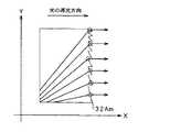
光源部20を構成する各発光ダイオード21は、それぞれ点光源として機能するため、各発光ダイオード21から出射された光は、図4に示すように、Y軸方向に放射状に広がる指向性を持って導光板10内に入射することになる。つまり、発光ダイオード21から出射され、光入射面11から入射された光は、導光板10の光の導光方向に対して、放射状に広がって進む指向性を有していることになる。このようにして入射した光は、プリズム12Anによって、上述したようにX軸方向成分が、光出射面13の法線方向に立ち上げられた偏向光となる。 Since each
この時、例えば、図4に示す偏向光L2a〜L2gのうち、偏向光L2a,L2bや、偏向光L2f,L2gといった、発光ダイオード21から広角でプリズム12Anに入射して偏向された光は、X軸方向には、光出射面13の法線近傍の方向へと立ち上げられた成分を持っているが、Y軸方向には、法線から非常に傾いた成分を持った偏向光となってしまう。 At this time, for example, among the deflected lights L2a to L2g shown in FIG. 4, the deflected lights L2a and L2b and the deflected lights L2f and L2g are incident on the prism 12An at a wide angle from the
したがって、このような偏向光が作る光出射面13の正面輝度は、図4に示すX軸方向に走るライン状の領域Kが高くなる不均一なものとなってしまう。例えば、図5に示すように光源部20が備える3つの発光ダイオード21a,21b,21cから導光板10の光入射面11に光を入射させ、光出射面13を正面から見た場合には、ライン状の領域Ka,Kb,Kcがストライプ状に現れることになる。 Therefore, the front luminance of the
このように、光出射面13から出力される光の正面輝度が、ライン状の領域で高くなってしまうような導光板10は、液晶表示装置のバックライトユニットの導光板として十分な機能を果たすことができない。 As described above, the
導光板10において、光出射面13の正面輝度がライン状に高い領域が生じてしまうのは、発光ダイオード21によって入射される光が指向性を持って、プリズム12Anに入射されるためであり、これにより、上述したように、プリズム12Anで光出射面13のX軸方向では法線方向に偏向されても、Y軸方向では、法線方向に偏向されない光もでてきてしまう。 In the
そこで、図1に示すように、バックライトユニット40では、光源部20の各発光ダイオード21から出射される光を導光板10の光入射面11に入射させる前段に光学素子30を配置し、導光板10に入射させる光の配光制御を行っている。 Therefore, as shown in FIG. 1, in the
図1に示すように、光学素子30は、光源部20の各発光ダイオード21からの光が入射される光入射面31に対向する光出射面32に、m個のプリズム32Am(mは、自然数)からなるプリズムパターンが形成されている。このプリズム32Amは、図2で示すZ軸方向を長手方向とする三角柱形状をしている。 As shown in FIG. 1, the
光学素子30の光出射面32に形成されるプリズム32Amは、連続したレンズ面を、階段状にすることで、厚みのあるレンズの光学的性質を変化させることなく薄型化したフレネルレンズとなっている。 The prism 32Am formed on the
光出射面32に形成するプリズム32Amは、光源部20の発光ダイオード21からY軸方向に放射状に広がる指向性を持って入射された光、つまり、導光板10の光の導光方向に対して放射状に広がって進む指向性を有する光を、図6に示すように、X軸方向、つまり、導光板10の光の導光方向と平行な方向に進む指向性を有する光に偏向するように設計される。このようなプリズム32Amを有する光学素子30を、光源20と、導光板10との間に挿入し、光源20から出射される光を光学素子30に入射させると、導光板10の光入射面11には、全面に渡って、光の導光方向と平行な方向に進む指向性を有する光が光学素子30から出射されて、入射されることになる。 The prism 32Am formed on the
これにより、導光板10内に入射された光は、導光板10の導光方向に対して放射状に広がって進む光を含まない。これにより、光反射面12に形成されているプリズム12Anに入射した場合に、上述したようにX軸方向の成分が光出射面13の法線方向となるように立ち上げられ、光出射面13から出射される光の正面輝度を、光出射面13全面に渡って均一化するようになる。 Thereby, the light incident on the
したがって、上述したように、光源20の発光ダイオード21から入射される光のうち、導光板10の光の導光方向に対して放射状に広がって進む指向性を有する光を、導光板10の光の導光方向と平行な方向に進む指向性を有する光に偏向するよう光学素子30のプリズム32Amを設計することで、上述した図4、図5を用いて示したようにストライプ状に現れる輝線を抑制する効果がある。 Therefore, as described above, of the light incident from the
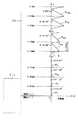
図7に、光学素子30の光出射面32に形成するプリズム32Amの具体的な設計値を示す。これは、図8に示すように光学素子30のX軸方向の厚みを6.0mmとし、光源20の各発光ダイオード21間のピッチを9.4mmとした場合のシミュレーション結果である。 FIG. 7 shows specific design values of the prism 32Am formed on the
プリズム32Amが、発光ダイオード21からY軸方向に放射状に広がる指向性を有して出射される全ての光を、X軸方向、つまり導光板10の光の導光方向と平行に進む指向性を有する光に偏向させるためには、プリズムパターンを、発光ダイオード21の中心からX軸に平行となる軸を対称軸として対称に形成する必要がある。 The prism 32Am has a directivity in which all light emitted from the
したがって、図8に示す発光ダイオード21bのように、当該発光ダイオード21bの中心からX軸方向に伸ばした対称軸に対して、上下それぞれ4.7mmの幅を持つ領域YO、領域YUに対称なプリズムパターンを形成することになる。図7に示す設計値は、発光ダイオード21の中心からX軸方向に伸びる対称軸に対して対称に形成するプリズムパターンのうち、上側領域又は下側領域のプリズムパターンの設計値となっている。Therefore, as the light-emitting
次に、図7に示すプリズム32Amの設計値を具体的に説明する。例えば、図7に示すプリズム32Amの設計値を、図8で示した発光ダイオード21bの中心からX軸方向に伸びる対称軸に対して上側の領域YOのプリズムパターンとした場合の様子を図9に示す。Next, the design value of the prism 32Am shown in FIG. 7 will be specifically described. For example, Figure a state when the design value of the prism 32Am shown in FIG. 7, and a prism pattern of the upper region YO symmetry axes extending in the X-axis direction from the center of the light-emitting
図9に示すように、プリズム32AmをプリズムPx(xは、自然数)とすると、図7の設計値に基づいて、Y軸方向、4.7mmの領域YOに、0.047mmのピッチで、プリズムP1〜P100の100個が形成されることになる。図9には、代表としてプリズムP1〜P4、P68、P69、P99、P100を示している。各プリズムPxは、図2で示したZ軸方向を長手方向とする三角柱形状をしており、図9には底面となる三角形が示されている。底面となる三角形の頂角、例えば、プリズムP68に示した頂角Aは、プリズムPxで全て同じ大きさの角度であり、48°となっている。As shown in FIG. 9, when the prism 32Am is a prism Px (x is a natural number), based on the design value of FIG. 7, the region YO in the Y-axis direction is 4.7 mm at a pitch of 0.047 mm. ,100 prisms P1 to P100 are formed. In FIG. 9, prisms P1 to P4 , P68 , P69 , P99 , and P100 are shown as representatives. Each prism Px has a triangular prism shape that the Z-axis direction shown in FIG. 2 and the longitudinal direction is shown a triangle which becomes the bottom surface in FIG. The apex angle of the triangle serving as the bottom surface, for example, the apex angle A shown in the prism P68 is an angle of the same magnitude in the prism Px and is 48 °.
図7で示す設計値の1つであるθは、図9のプリズムP68に示すように、プリズムPxの底面となる三角形の底角のうちの1つを示している。上述したように頂角が一定であることから、この底角θを可変させることで、プリズムの形状が決定されることになる。なお、図9で示す、発光ダイオード21bの中心からX軸方向に伸びる対称軸に対して下側の領域YUには、領域YOと対称のプリズムパターンが形成されることになる。Θ is one of the design values shown in FIG. 7, as shown in the prism P68 in FIG. 9 shows one of the base angles of the triangle which is a bottom surface of the prism Px. Since the apex angle is constant as described above, the prism shape is determined by varying the base angle θ. Incidentally, it is shown in Figure 9, the lower region YU with respect to the central X-axis symmetry axis extending in the direction from the light-emitting
このようにして光学素子30には、各発光ダイオード21の中心からX軸方向に伸びる対称軸と対称に、例えば、図7に示した設計値に基づいてプリズム32Amを形成することで、発光ダイオード21から入射された、導光板10の光の導光方向に対して放射状に広がって進む指向性を有する光を、導光板10の光の導光方向と平行な方向へと進む指向性を有する光に偏向することができる。 Thus, the
光学素子30を形成する材料としては、光源20から入射した光を全反射させて、効率よく導光するために、屈折率が1.44〜1.45を下限とし、これ以上の屈折率値を有する材料が選択されることになる。例えば、導光板10を形成する際にも使用されるアクリル樹脂は、屈折率が1.49であり、射出成形可能な材料でもある。光学素子30は、光出射面32にプリズム32Amを形成する必要があるため、射出成形が可能な、このアクリル樹脂を用いれば、容易にプリズム32Amが形成できるため、低コストで大量生産が可能となる。 As a material for forming the
次に、光学素子30による効果を検証するため、図7に示す設計値に基づいてプリズム32Amを形成した光学素子30を用いた場合の導光板10の正面輝度をシミュレーションにより算出した。発光ダイオード21a,21b,21cとしては、日亜化学社製、白色発光ダイオード(NSCW−215シリーズ)を用い、15mAの電流を印加するものとする。 Next, in order to verify the effect of the
図10に、シミュレーション結果として、導光板10の光出射面13の輝度分布を示す。図10に示すように、光出射面13の輝度分布は、5000cd/m2程度の輝度となる領域G1、4000cd/m2程度の輝度となる領域G2、3000cd/m2程度の輝度となる領域G3という3つの異なる輝度領域が現れた分布となる。領域G1は、各発光ダイオード21から出射された光のうちX軸方向と平行に出射された光が到達した領域であり、領域G2は、発光ダイオード21から出射された光のうちY軸方向にやや拡散した光が光学素子30で偏向されて到達した領域であり、領域G3は、発光ダイオード21から出射された光のうち、領域G2に到達した光よりもさらに、Y軸方向に拡散した光が光学素子30で偏向されて到達した領域である。FIG. 10 shows the luminance distribution of the
図10に示すように、光出射面32にプリズム32Amが形成された光学素子30を用いると、導光板10の光出射面13から出射される光による正面輝度は、輝度の異なる領域(領域G1,G2,G3)が生じるが、導光板10の光出射面13全面に渡って、平均して3000cd/m2の輝度を獲得することが可能となる。この正面輝度の向上は、光学素子30のプリズム32Amによって、導光板10の光の導光方向に対して放射状に進む指向性を有する光が、導光板10の光の導光方向と平行な方向へと進む指向性を有する光となったことで、導光板10の側面からの出射損失が大幅に軽減した結果であると考えられ、光の利用効率が非常に高くなっていることを示している。As shown in FIG. 10, when an
このように、光学素子30を用いることで、図4,5を用いて説明をしたような、ストライプ状の輝線として現れる輝度ムラが抑制されていることが分かる。例えば、上述したように、光反射面12に、断面形状が光反射面12側を底辺とする三角形で、上記三角形の光入射面11側の底角が角度α=50°〜60°、他方の底角が角度β=70°〜90°となる溝を複数作製して、プリズム12Anを光反射面12上に形成すると、X軸方向の光の立ち上げが効果的に行われ、ストライプ状の輝線が際立って出現することになるため、光学素子30を用いると特に有効となる。 Thus, it can be seen that the use of the
また、光反射面12に、断面形状が、従来の技術として一般に用いられている角度α=角度β=45°の三角形となる複数の溝を形成した場合にも、光学素子30を用いることで、点光源である発光ダイオード21を用いた場合にストライプ状の輝線として現れる輝度ムラを抑制することができる。 Even when a plurality of grooves whose cross-sectional shape is a triangle having an angle α = angle β = 45 °, which is generally used as a conventional technique, is formed on the
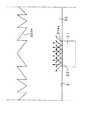
図10に示した領域G1,G2,G3の輝度分布の相違は、図11に示すように発光ダイオード21の光出射面22と接触する光学素子30の光入射面31上に、拡散プリズムとしてシリンドリカルレンズ31As(Sは、自然数)を複数個形成し、光学素子30に入射する光を拡散させることで制御することができる。発光ダイオード21から出射され、シリンドリカルレンズ31Asを介して光学素子30内を導光される光は、Y軸方向へ広がる指向性を有しつつ拡散されてプリズム32Amに入射される。したがって、シリンドリカルレンズ31As及びプリズム32Amを介して、導光板10の光入射面11に入射される光は、導光板10の光入射面11全面に渡って均一に拡散され、且つ、導光板10の光の導光方向と平行な方向に進む指向性を有するように偏向された光となっている。これにより、導光板10の光出射面13から出射される光の輝度分布を、高輝度且つ均一にすることができる。 The difference in luminance distribution between the regions G1, G2, and G3 shown in FIG. 10 is that a cylindrical prism as a diffusion prism is formed on the
このような、光学素子30を備えるバックライト装置40は、光源部20が有する各発光ダイオード21から出射された光を、光学素子30でX軸に平行な指向性を有する光に偏向することでY軸方向の配光制御をして、導光板10の光入射面11から入射させる。導光板10に入射した光は、光反射面12、反射シート15で反射して、光出射面13から出射される。このとき、導光板10内の光反射面12では、プリズム12Anに入射した光のX軸方向成分が配光制御され、光反射面13の法線方向に立ち上げられて集光される。 Such a
したがって、導光板10内では、光学素子30によってY軸方向の配光制御がなされた光が、導光板10内でプリズム12AnによってX軸方向へ立ち上げられながら導光されると共に、光出射面13から出射されることになる。光出射面13から出射された光は、フレーム35に開口された開口部35Aから、例えば、液晶表示装置などに照射される。 Therefore, in the
このように、バックライトユニット40は、例えば、従来の技術で示したバックライトユニット100が有する、拡散シート102、Y軸方向の光の成分を光出射面83の法線方向へ集光する第1のレンズシート103、X軸方向の光の成分を光出射面83の法線方向へ集光する第2のレンズシート104が不要となるため、大幅なコストダウン及び当該バックライトユニット40を薄型化することができる。 Thus, for example, the
これは、光学素子30の光出射面32に形成するプリズム32Amのプリズムパターンを、Y軸方向へ広がる指向性のある光を、X軸方向に平行な光に偏向、つまり導光板10の光の導光方向と平行な方向に進む指向性を有する光に偏向してY軸方向の配光制御をするように設計し、さらには、導光板10の光反射面12にプリズム12Anを形成するために作製する溝の断面形状を、光反射面12側を底辺とし、光入射面11側の底角が角度α=50°〜60°、他方の底角が角度β=70°〜90°である三角形となるように、適切に設計し配光制御をすることで、レンズシートを用いた場合と同じ程度の正面輝度を得られるほど十分となるからである。これにより、バックライトユニット40は、光出射面13全面に渡って、十分な正面輝度を獲得することができる。 This is because the prism pattern of the prism 32Am formed on the
光反射面12に形成されるプリズムパターンは、プリズム12An以外の形状であってもよく、本発明はこのプリズムパターンに限定されるものではない。 The prism pattern formed on the
例えば、断面形状が三角形である溝を作製することで光反射面12上にプリズム12Anを形成する場合には、角度α、角度βの値を、角度α=50°〜60°、角度β=70°〜90°以外の値に変更してプリズムパターンを形成してもよい。また、以下に示すような断面形状の溝を作製することで形成したプリズムパターンなどを用いてもよい。 For example, in the case where the prism 12An is formed on the
例えば、光反射面12に作製する溝の断面形状を図12に示すように、ラウンドを持たせた台形のような断面形状45としたり、図13に示すように2つの三角形からなる断面形状46としたり、図14に示すように一辺が任意の凹凸を有する台形のような断面形状47とすることで形成されたプリズムパターンなども用いてもよい。 For example, the cross-sectional shape of the groove formed in the
さらに、また、光学素子30を用いてバックライトユニットを構成した場合であっても、従来の技術で説明した拡散シート102、第1のレンズシート103、第2のレンズシート104といったシート類を適宜用いて導光板の光出射面から出射された出射光を整えるようにしてもかまわない。 Furthermore, even when a backlight unit is configured using the
10 導光板、11 光入射面、12 光反射面、12An(nは、自然数) プリズム、13 光出射面、20 光源部、30 光学素子、31 光入射面、32 光出射面、32Am(mは、自然数) プリズム、40 バックライトユニット
DESCRIPTION OF
Claims (9)
Translated fromJapanese光源より出射される光を入射し、入射された光のうち、上記導光板の光の導光方向に対して、放射状に広がって進む指向性を有する光を、上記導光板の上記光の導光方向と平行な方向へと進む指向性を有する光に偏向して、出射し、上記導光板の上記光入射面に入射させる光学手段を備えること
を特徴とする光学素子。One side is a light incident surface, and the light incident from the light incident surface is totally reflected by the light exit surface as one main surface and the light reflection surface as the other main surface, and guided from the light exit surface. An optical element that adjusts light incident on the light incident surface of the light guide plate that emits light,
The light emitted from the light source is incident. Of the incident light, the light having directivity that spreads radially with respect to the light guide direction of the light of the light guide plate is guided by the light of the light guide plate. An optical element comprising: an optical unit that deflects and emits light having directivity that travels in a direction parallel to the light direction and enters the light incident surface of the light guide plate.
を特徴とする請求項1記載の光学素子。2. The optical element according to claim 1, wherein the optical means is a Fresnel lens including a plurality of prisms formed in a longitudinal direction of a light exit surface of the optical element in contact with the light incident surface of the light guide plate. .
を特徴とする請求項1記載の光学素子。The optical element according to claim 1, further comprising a diffusion prism that diffuses incident light on a light incident surface of the optical element on which light from the light source is incident.
上記導光板の上記光入射面の長手方向に所定の間隔で配列された複数の発光素子を有する光源と、
上記光源の上記複数の発光素子より出射された光を入射し、上記導光板の上記光入射面への入射光として出射する光学素子と、
上記導光板の上記光反射面側に配置される反射シートと、
上記導光板に、上記光源と、上記光学素子と、上記反射シートとを保持するフレームとを備え、
上記導光板は、上記光の入射方向をX軸方向とし、上記X軸方向に直交して上記光出射面に平行な方向をY軸方向とし、上記X軸方向及び上記Y軸方向に垂直な方向を法線方向とするとき、上記光入射面から入射された光を、上記X軸方向の傾きが上記法線方向に対してゼロに近付くように偏向して、上記光出射面から出射させる配光制御をするX軸方向配光制御手段を有し、
上記光学素子は、上記入射された光のうち、上記導光板の光の導光方向に対して、放射状に広がって進む指向性を有する光を、上記導光板の上記光の導光方向と平行な方向へと進む指向性を有する光に偏向して、出射し、上記導光板の上記光入射面に入射させる光学手段を有すること
を特徴とするバックライト装置。One side is a light incident surface, and the light incident from the light incident surface is totally reflected by the light exit surface as one main surface and the light reflection surface as the other main surface, and guided from the light exit surface. A light guide plate for surface emission;
A light source having a plurality of light emitting elements arranged at predetermined intervals in the longitudinal direction of the light incident surface of the light guide plate;
An optical element that receives light emitted from the plurality of light emitting elements of the light source and emits light as incident light on the light incident surface of the light guide plate;
A reflective sheet disposed on the light reflecting surface side of the light guide plate;
The light guide plate includes the light source, the optical element, and a frame that holds the reflection sheet.
The light guide plate has an incident direction of the light as an X-axis direction, a direction perpendicular to the X-axis direction and parallel to the light emitting surface as a Y-axis direction, and perpendicular to the X-axis direction and the Y-axis direction. When the direction is the normal direction, the light incident from the light incident surface is deflected so that the inclination in the X-axis direction approaches zero with respect to the normal direction, and is emitted from the light emitting surface. X-axis direction light distribution control means for performing light distribution control,
The optical element emits light having directivity that spreads radially in the light guide direction of the light of the light guide plate among the incident light and is parallel to the light guide direction of the light of the light guide plate. A backlight device comprising: an optical unit that deflects and emits light having directivity that travels in any direction, and causes the light to enter the light incident surface of the light guide plate.
を特徴とする請求項4記載のバックライト装置。The optical means of the optical element is a Fresnel lens composed of a plurality of prisms formed in the longitudinal direction of the light emitting surface of the optical element in contact with the light incident surface of the light guide plate. The backlight device described.
を特徴とする請求項4記載のバックライト装置。The backlight device according to claim 4, wherein the optical element has a diffusion prism that diffuses incident light on a light incident surface of the optical element on which light from the light source is incident.
を特徴とする請求項4記載のバックライト装置。The X-axis direction light distribution control means of the light guide plate is a plurality of prisms formed in the X-axis direction on the light reflecting surface and having a longitudinal direction in the Y-axis direction. 4. The backlight device according to 4.
上記溝は、当該溝の断面形状が上記光反射面側を底辺とする三角形で、上記三角形の上記光入射面側の底角αがα=50°〜60°、他方の底角βがβ=70°〜90°の角度であること
を特徴とする請求項7記載のバックライト装置。The prism is formed by forming a plurality of grooves having a predetermined shape with the Y-axis direction as a longitudinal direction on the light reflecting surface in the X-axis direction,
The groove has a triangular cross-sectional shape with the light reflecting surface side as the base, the base angle α of the triangle on the light incident surface side is α = 50 ° to 60 °, and the other base angle β is β The backlight device according to claim 7, wherein the angle is 70 ° to 90 °.
を特徴とする請求項4記載のバックライト装置。
The backlight device according to claim 4, wherein the plurality of light emitting elements included in the light source are light emitting diodes (LEDs).
Priority Applications (1)
| Application Number | Priority Date | Filing Date | Title |
|---|---|---|---|
| JP2003372753AJP2005135844A (en) | 2003-10-31 | 2003-10-31 | Optical element and backlight device |
Applications Claiming Priority (1)
| Application Number | Priority Date | Filing Date | Title |
|---|---|---|---|
| JP2003372753AJP2005135844A (en) | 2003-10-31 | 2003-10-31 | Optical element and backlight device |
Publications (1)
| Publication Number | Publication Date |
|---|---|
| JP2005135844Atrue JP2005135844A (en) | 2005-05-26 |
Family
ID=34649039
Family Applications (1)
| Application Number | Title | Priority Date | Filing Date |
|---|---|---|---|
| JP2003372753APendingJP2005135844A (en) | 2003-10-31 | 2003-10-31 | Optical element and backlight device |
Country Status (1)
| Country | Link |
|---|---|
| JP (1) | JP2005135844A (en) |
Cited By (50)
| Publication number | Priority date | Publication date | Assignee | Title |
|---|---|---|---|---|
| JP2006012800A (en)* | 2004-05-28 | 2006-01-12 | Sun Tec Kk | Refraction-condensing plate for backlight |
| WO2007140077A1 (en)* | 2006-05-24 | 2007-12-06 | 3M Innovative Properties Company | Backlight wedge with adjacent reflective surfaces |
| WO2007140076A1 (en)* | 2006-05-24 | 2007-12-06 | 3M Innovative Properties Company | Backlight wedge with side mounted light source |
| WO2007140092A1 (en)* | 2006-05-24 | 2007-12-06 | 3M Innovative Properties Company | Backlight asymmetric light input wedge |
| WO2007140087A1 (en)* | 2006-05-24 | 2007-12-06 | 3M Innovative Properties Company | Backlight wedge with encapsulated light source |
| WO2008102762A1 (en)* | 2007-02-20 | 2008-08-28 | Nobuo Oyama | Light source apparatus, lighting apparatus using the light source apparatus, and plant growing apparatus using lighting apparatus |
| WO2009054160A1 (en)* | 2007-10-23 | 2009-04-30 | Sharp Kabushiki Kaisha | Backlight unit and display unit |
| JP2009259653A (en)* | 2008-04-17 | 2009-11-05 | Citizen Electronics Co Ltd | Linear light source, planar light unit, and display |
| KR101165128B1 (en) | 2008-09-30 | 2012-07-12 | 코오롱인더스트리 주식회사 | Diffuser Plate |
| CN102767754A (en)* | 2012-06-25 | 2012-11-07 | 中航华东光电有限公司 | Backlight module structure |
| WO2013173760A1 (en)* | 2012-05-18 | 2013-11-21 | Reald Inc. | Source conditioning for imaging directional backlights |
| US8651726B2 (en) | 2010-11-19 | 2014-02-18 | Reald Inc. | Efficient polarized directional backlight |
| US8917441B2 (en) | 2012-07-23 | 2014-12-23 | Reald Inc. | Observe tracking autostereoscopic display |
| US9188731B2 (en) | 2012-05-18 | 2015-11-17 | Reald Inc. | Directional backlight |
| US9235057B2 (en) | 2012-05-18 | 2016-01-12 | Reald Inc. | Polarization recovery in a directional display device |
| US9237337B2 (en) | 2011-08-24 | 2016-01-12 | Reald Inc. | Autostereoscopic display with a passive cycloidal diffractive waveplate |
| US9250448B2 (en) | 2010-11-19 | 2016-02-02 | Reald Inc. | Segmented directional backlight and related methods of backlight illumination |
| US9350980B2 (en) | 2012-05-18 | 2016-05-24 | Reald Inc. | Crosstalk suppression in a directional backlight |
| US9420266B2 (en) | 2012-10-02 | 2016-08-16 | Reald Inc. | Stepped waveguide autostereoscopic display apparatus with a reflective directional element |
| US9429764B2 (en) | 2012-05-18 | 2016-08-30 | Reald Inc. | Control system for a directional light source |
| US9436015B2 (en) | 2012-12-21 | 2016-09-06 | Reald Inc. | Superlens component for directional display |
| US9482874B2 (en) | 2010-11-19 | 2016-11-01 | Reald Inc. | Energy efficient directional flat illuminators |
| US9551825B2 (en) | 2013-11-15 | 2017-01-24 | Reald Spark, Llc | Directional backlights with light emitting element packages |
| US9594261B2 (en) | 2012-05-18 | 2017-03-14 | Reald Spark, Llc | Directionally illuminated waveguide arrangement |
| US9678267B2 (en) | 2012-05-18 | 2017-06-13 | Reald Spark, Llc | Wide angle imaging directional backlights |
| US9709723B2 (en) | 2012-05-18 | 2017-07-18 | Reald Spark, Llc | Directional backlight |
| US9739928B2 (en) | 2013-10-14 | 2017-08-22 | Reald Spark, Llc | Light input for directional backlight |
| US9740034B2 (en) | 2013-10-14 | 2017-08-22 | Reald Spark, Llc | Control of directional display |
| US9835792B2 (en) | 2014-10-08 | 2017-12-05 | Reald Spark, Llc | Directional backlight |
| US9872007B2 (en) | 2013-06-17 | 2018-01-16 | Reald Spark, Llc | Controlling light sources of a directional backlight |
| TWI622811B (en)* | 2013-02-22 | 2018-05-01 | 瑞爾D斯帕克有限責任公司 | Directional backlight |
| US10062357B2 (en) | 2012-05-18 | 2018-08-28 | Reald Spark, Llc | Controlling light sources of a directional backlight |
| US10126575B1 (en) | 2017-05-08 | 2018-11-13 | Reald Spark, Llc | Optical stack for privacy display |
| US10228505B2 (en) | 2015-05-27 | 2019-03-12 | Reald Spark, Llc | Wide angle imaging directional backlights |
| US10303030B2 (en) | 2017-05-08 | 2019-05-28 | Reald Spark, Llc | Reflective optical stack for privacy display |
| US10321123B2 (en) | 2016-01-05 | 2019-06-11 | Reald Spark, Llc | Gaze correction of multi-view images |
| US10330843B2 (en) | 2015-11-13 | 2019-06-25 | Reald Spark, Llc | Wide angle imaging directional backlights |
| US10356383B2 (en) | 2014-12-24 | 2019-07-16 | Reald Spark, Llc | Adjustment of perceived roundness in stereoscopic image of a head |
| US10359561B2 (en) | 2015-11-13 | 2019-07-23 | Reald Spark, Llc | Waveguide comprising surface relief feature and directional backlight, directional display device, and directional display apparatus comprising said waveguide |
| US10359560B2 (en) | 2015-04-13 | 2019-07-23 | Reald Spark, Llc | Wide angle imaging directional backlights |
| US10393946B2 (en) | 2010-11-19 | 2019-08-27 | Reald Spark, Llc | Method of manufacturing directional backlight apparatus and directional structured optical film |
| US10459321B2 (en) | 2015-11-10 | 2019-10-29 | Reald Inc. | Distortion matching polarization conversion systems and methods thereof |
| US10475418B2 (en) | 2015-10-26 | 2019-11-12 | Reald Spark, Llc | Intelligent privacy system, apparatus, and method thereof |
| US10627670B2 (en) | 2018-01-25 | 2020-04-21 | Reald Spark, Llc | Reflective optical stack for privacy display |
| US10788710B2 (en) | 2017-09-15 | 2020-09-29 | Reald Spark, Llc | Optical stack for switchable directional display |
| US11067736B2 (en) | 2014-06-26 | 2021-07-20 | Reald Spark, Llc | Directional privacy display |
| US11327358B2 (en) | 2017-05-08 | 2022-05-10 | Reald Spark, Llc | Optical stack for directional display |
| US11821602B2 (en) | 2020-09-16 | 2023-11-21 | Reald Spark, Llc | Vehicle external illumination device |
| US11966049B2 (en) | 2022-08-02 | 2024-04-23 | Reald Spark, Llc | Pupil tracking near-eye display |
| US12282168B2 (en) | 2022-08-11 | 2025-04-22 | Reald Spark, Llc | Anamorphic directional illumination device with selective light-guiding |
- 2003
- 2003-10-31JPJP2003372753Apatent/JP2005135844A/enactivePending
Cited By (89)
| Publication number | Priority date | Publication date | Assignee | Title |
|---|---|---|---|---|
| JP2006012800A (en)* | 2004-05-28 | 2006-01-12 | Sun Tec Kk | Refraction-condensing plate for backlight |
| US8059933B2 (en) | 2006-05-24 | 2011-11-15 | 3M Innovative Properties Company | Backlight asymmetric light input wedge |
| US9008486B2 (en) | 2006-05-24 | 2015-04-14 | 3M Innovative Properties Company | Backlight asymmetric light input wedge |
| WO2007140092A1 (en)* | 2006-05-24 | 2007-12-06 | 3M Innovative Properties Company | Backlight asymmetric light input wedge |
| WO2007140087A1 (en)* | 2006-05-24 | 2007-12-06 | 3M Innovative Properties Company | Backlight wedge with encapsulated light source |
| US7941028B2 (en) | 2006-05-24 | 2011-05-10 | 3M Innovative Properties Company | Backlight asymmetric light input wedge |
| WO2007140077A1 (en)* | 2006-05-24 | 2007-12-06 | 3M Innovative Properties Company | Backlight wedge with adjacent reflective surfaces |
| US9207384B2 (en) | 2006-05-24 | 2015-12-08 | 3M Innovative Properties Company | Backlight asymmetric light input wedge |
| US8920015B2 (en) | 2006-05-24 | 2014-12-30 | 3M Innovative Properties Company | Backlight wedge with adjacent reflective surfaces |
| US7660509B2 (en) | 2006-05-24 | 2010-02-09 | 3M Innovative Properties Company | Backlight asymmetric light input wedge |
| US7740387B2 (en) | 2006-05-24 | 2010-06-22 | 3M Innovative Properties Company | Backlight wedge with side mounted light source |
| WO2007140076A1 (en)* | 2006-05-24 | 2007-12-06 | 3M Innovative Properties Company | Backlight wedge with side mounted light source |
| US7607814B2 (en) | 2006-05-24 | 2009-10-27 | 3M Innovative Properties Company | Backlight with symmetric wedge shaped light guide input portion with specular reflective surfaces |
| WO2008102762A1 (en)* | 2007-02-20 | 2008-08-28 | Nobuo Oyama | Light source apparatus, lighting apparatus using the light source apparatus, and plant growing apparatus using lighting apparatus |
| US8376601B2 (en) | 2007-10-23 | 2013-02-19 | Sharp Kabushiki Kaisha | Backlight unit and display unit |
| WO2009054160A1 (en)* | 2007-10-23 | 2009-04-30 | Sharp Kabushiki Kaisha | Backlight unit and display unit |
| JP2009259653A (en)* | 2008-04-17 | 2009-11-05 | Citizen Electronics Co Ltd | Linear light source, planar light unit, and display |
| KR101165128B1 (en) | 2008-09-30 | 2012-07-12 | 코오롱인더스트리 주식회사 | Diffuser Plate |
| US10393946B2 (en) | 2010-11-19 | 2019-08-27 | Reald Spark, Llc | Method of manufacturing directional backlight apparatus and directional structured optical film |
| US10473947B2 (en) | 2010-11-19 | 2019-11-12 | Reald Spark, Llc | Directional flat illuminators |
| US9519153B2 (en) | 2010-11-19 | 2016-12-13 | Reald Inc. | Directional flat illuminators |
| US8651726B2 (en) | 2010-11-19 | 2014-02-18 | Reald Inc. | Efficient polarized directional backlight |
| US9482874B2 (en) | 2010-11-19 | 2016-11-01 | Reald Inc. | Energy efficient directional flat illuminators |
| US9250448B2 (en) | 2010-11-19 | 2016-02-02 | Reald Inc. | Segmented directional backlight and related methods of backlight illumination |
| US9237337B2 (en) | 2011-08-24 | 2016-01-12 | Reald Inc. | Autostereoscopic display with a passive cycloidal diffractive waveplate |
| US10048500B2 (en) | 2012-05-18 | 2018-08-14 | Reald Spark, Llc | Directionally illuminated waveguide arrangement |
| US10062357B2 (en) | 2012-05-18 | 2018-08-28 | Reald Spark, Llc | Controlling light sources of a directional backlight |
| US9350980B2 (en) | 2012-05-18 | 2016-05-24 | Reald Inc. | Crosstalk suppression in a directional backlight |
| US9235057B2 (en) | 2012-05-18 | 2016-01-12 | Reald Inc. | Polarization recovery in a directional display device |
| US9429764B2 (en) | 2012-05-18 | 2016-08-30 | Reald Inc. | Control system for a directional light source |
| US10902821B2 (en) | 2012-05-18 | 2021-01-26 | Reald Spark, Llc | Controlling light sources of a directional backlight |
| US9188731B2 (en) | 2012-05-18 | 2015-11-17 | Reald Inc. | Directional backlight |
| CN104302965A (en)* | 2012-05-18 | 2015-01-21 | 瑞尔D股份有限公司 | Light Source Conditioning for Imaging Directional Backlights |
| US9541766B2 (en) | 2012-05-18 | 2017-01-10 | Reald Spark, Llc | Directional display apparatus |
| US10365426B2 (en) | 2012-05-18 | 2019-07-30 | Reald Spark, Llc | Directional backlight |
| US9594261B2 (en) | 2012-05-18 | 2017-03-14 | Reald Spark, Llc | Directionally illuminated waveguide arrangement |
| CN104302965B (en)* | 2012-05-18 | 2017-04-12 | 瑞尔D斯帕克有限责任公司 | Light Source Conditioning for Imaging Directional Backlights |
| US9678267B2 (en) | 2012-05-18 | 2017-06-13 | Reald Spark, Llc | Wide angle imaging directional backlights |
| US9709723B2 (en) | 2012-05-18 | 2017-07-18 | Reald Spark, Llc | Directional backlight |
| US11287878B2 (en) | 2012-05-18 | 2022-03-29 | ReaID Spark, LLC | Controlling light sources of a directional backlight |
| WO2013173760A1 (en)* | 2012-05-18 | 2013-11-21 | Reald Inc. | Source conditioning for imaging directional backlights |
| US10175418B2 (en) | 2012-05-18 | 2019-01-08 | Reald Spark, Llc | Wide angle imaging directional backlights |
| US11681359B2 (en) | 2012-05-18 | 2023-06-20 | Reald Spark, Llc | Controlling light sources of a directional backlight |
| US9910207B2 (en) | 2012-05-18 | 2018-03-06 | Reald Spark, Llc | Polarization recovery in a directional display device |
| US10712582B2 (en) | 2012-05-18 | 2020-07-14 | Reald Spark, Llc | Directional display apparatus |
| CN102767754A (en)* | 2012-06-25 | 2012-11-07 | 中航华东光电有限公司 | Backlight module structure |
| US8917441B2 (en) | 2012-07-23 | 2014-12-23 | Reald Inc. | Observe tracking autostereoscopic display |
| US9420266B2 (en) | 2012-10-02 | 2016-08-16 | Reald Inc. | Stepped waveguide autostereoscopic display apparatus with a reflective directional element |
| US9436015B2 (en) | 2012-12-21 | 2016-09-06 | Reald Inc. | Superlens component for directional display |
| US10054732B2 (en) | 2013-02-22 | 2018-08-21 | Reald Spark, Llc | Directional backlight having a rear reflector |
| TWI622811B (en)* | 2013-02-22 | 2018-05-01 | 瑞爾D斯帕克有限責任公司 | Directional backlight |
| CN111487707A (en)* | 2013-02-22 | 2020-08-04 | 瑞尔D斯帕克有限责任公司 | directional backlight |
| US9872007B2 (en) | 2013-06-17 | 2018-01-16 | Reald Spark, Llc | Controlling light sources of a directional backlight |
| US10488578B2 (en) | 2013-10-14 | 2019-11-26 | Reald Spark, Llc | Light input for directional backlight |
| US9740034B2 (en) | 2013-10-14 | 2017-08-22 | Reald Spark, Llc | Control of directional display |
| US9739928B2 (en) | 2013-10-14 | 2017-08-22 | Reald Spark, Llc | Light input for directional backlight |
| US9551825B2 (en) | 2013-11-15 | 2017-01-24 | Reald Spark, Llc | Directional backlights with light emitting element packages |
| US10185076B2 (en) | 2013-11-15 | 2019-01-22 | Reald Spark, Llc | Directional backlights with light emitting element packages |
| US11067736B2 (en) | 2014-06-26 | 2021-07-20 | Reald Spark, Llc | Directional privacy display |
| US9835792B2 (en) | 2014-10-08 | 2017-12-05 | Reald Spark, Llc | Directional backlight |
| US10356383B2 (en) | 2014-12-24 | 2019-07-16 | Reald Spark, Llc | Adjustment of perceived roundness in stereoscopic image of a head |
| US10359560B2 (en) | 2015-04-13 | 2019-07-23 | Reald Spark, Llc | Wide angle imaging directional backlights |
| US10634840B2 (en) | 2015-04-13 | 2020-04-28 | Reald Spark, Llc | Wide angle imaging directional backlights |
| US10459152B2 (en) | 2015-04-13 | 2019-10-29 | Reald Spark, Llc | Wide angle imaging directional backlights |
| US11061181B2 (en) | 2015-04-13 | 2021-07-13 | Reald Spark, Llc | Wide angle imaging directional backlights |
| US10228505B2 (en) | 2015-05-27 | 2019-03-12 | Reald Spark, Llc | Wide angle imaging directional backlights |
| US10475418B2 (en) | 2015-10-26 | 2019-11-12 | Reald Spark, Llc | Intelligent privacy system, apparatus, and method thereof |
| US11030981B2 (en) | 2015-10-26 | 2021-06-08 | Reald Spark, Llc | Intelligent privacy system, apparatus, and method thereof |
| US10459321B2 (en) | 2015-11-10 | 2019-10-29 | Reald Inc. | Distortion matching polarization conversion systems and methods thereof |
| US10359561B2 (en) | 2015-11-13 | 2019-07-23 | Reald Spark, Llc | Waveguide comprising surface relief feature and directional backlight, directional display device, and directional display apparatus comprising said waveguide |
| US10712490B2 (en) | 2015-11-13 | 2020-07-14 | Reald Spark, Llc | Backlight having a waveguide with a plurality of extraction facets, array of light sources, a rear reflector having reflective facets and a transmissive sheet disposed between the waveguide and reflector |
| US10330843B2 (en) | 2015-11-13 | 2019-06-25 | Reald Spark, Llc | Wide angle imaging directional backlights |
| US11067738B2 (en) | 2015-11-13 | 2021-07-20 | Reald Spark, Llc | Surface features for imaging directional backlights |
| US10750160B2 (en) | 2016-01-05 | 2020-08-18 | Reald Spark, Llc | Gaze correction of multi-view images |
| US10321123B2 (en) | 2016-01-05 | 2019-06-11 | Reald Spark, Llc | Gaze correction of multi-view images |
| US11327358B2 (en) | 2017-05-08 | 2022-05-10 | Reald Spark, Llc | Optical stack for directional display |
| US10126575B1 (en) | 2017-05-08 | 2018-11-13 | Reald Spark, Llc | Optical stack for privacy display |
| US10303030B2 (en) | 2017-05-08 | 2019-05-28 | Reald Spark, Llc | Reflective optical stack for privacy display |
| US11016318B2 (en) | 2017-05-08 | 2021-05-25 | Reald Spark, Llc | Optical stack for switchable directional display |
| US11092851B2 (en) | 2017-09-15 | 2021-08-17 | Reald Spark, Llc | Optical stack for switchable directional display |
| US11181780B2 (en) | 2017-09-15 | 2021-11-23 | Reald Spark, Llc | Optical stack for switchable directional display |
| US10788710B2 (en) | 2017-09-15 | 2020-09-29 | Reald Spark, Llc | Optical stack for switchable directional display |
| US10976578B2 (en) | 2018-01-25 | 2021-04-13 | Reald Spark, Llc | Reflective optical stack for privacy display |
| US10712608B2 (en) | 2018-01-25 | 2020-07-14 | Reald Spark, Llc | Reflective optical stack for privacy display |
| US10627670B2 (en) | 2018-01-25 | 2020-04-21 | Reald Spark, Llc | Reflective optical stack for privacy display |
| US11821602B2 (en) | 2020-09-16 | 2023-11-21 | Reald Spark, Llc | Vehicle external illumination device |
| US12222077B2 (en) | 2020-09-16 | 2025-02-11 | Reald Spark, Llc | Vehicle external illumination device |
| US11966049B2 (en) | 2022-08-02 | 2024-04-23 | Reald Spark, Llc | Pupil tracking near-eye display |
| US12282168B2 (en) | 2022-08-11 | 2025-04-22 | Reald Spark, Llc | Anamorphic directional illumination device with selective light-guiding |
Similar Documents
| Publication | Publication Date | Title |
|---|---|---|
| JP2005135844A (en) | Optical element and backlight device | |
| JP4273930B2 (en) | Light guide plate and backlight device | |
| US7522809B2 (en) | Planar light source and light guide for use therein | |
| US7507011B2 (en) | Surface light source equipment and apparatus using the same | |
| JP4006918B2 (en) | Surface light source device and manufacturing method thereof | |
| JP5510038B2 (en) | Collimated light source and surface light source device | |
| KR100723857B1 (en) | Light guide plate, surface light source device, and display device | |
| KR101607287B1 (en) | Light guiding plate, backlight assembly and display apparatus having the same | |
| JP2004319482A (en) | Light guide plate including light deflecting member and side emission type backlight device | |
| JP4172008B2 (en) | Surface light source device | |
| KR20130004178A (en) | Symmetric serrated edge light guide film having elliptical base segments | |
| JP2005085671A (en) | Light guide plate and plane light source device | |
| JP5853739B2 (en) | Collimated light source and surface light source device | |
| JP2005063913A (en) | Light guide plate | |
| US8885118B2 (en) | Illumination device and liquid crystal display having a light guide plate with protrusions of multiple heights | |
| JP2004152496A (en) | Light guide plate | |
| US20170285244A1 (en) | Planar illumination device | |
| JP4389529B2 (en) | Surface illumination device and light guide plate | |
| JP2005063912A (en) | Light guide plate and its manufacturing method | |
| JP2011258362A (en) | Surface light source device | |
| US20170123130A1 (en) | Light guide plate, backlight module and display device | |
| KR101472338B1 (en) | Backlight Unit | |
| JP6751452B2 (en) | Area lighting device | |
| CN117255911A (en) | Planar lighting device | |
| JP2004079418A (en) | Light guide plate and backlight device using the same |
Legal Events
| Date | Code | Title | Description |
|---|---|---|---|
| A621 | Written request for application examination | Free format text:JAPANESE INTERMEDIATE CODE: A621 Effective date:20060830 | |
| A977 | Report on retrieval | Free format text:JAPANESE INTERMEDIATE CODE: A971007 Effective date:20081112 | |
| A131 | Notification of reasons for refusal | Free format text:JAPANESE INTERMEDIATE CODE: A131 Effective date:20081224 | |
| A521 | Written amendment | Free format text:JAPANESE INTERMEDIATE CODE: A523 Effective date:20090219 | |
| A02 | Decision of refusal | Free format text:JAPANESE INTERMEDIATE CODE: A02 Effective date:20090818 |