JP2005129607A - Wafer division method - Google Patents
Wafer division methodDownload PDFInfo
- Publication number
- JP2005129607A JP2005129607AJP2003361471AJP2003361471AJP2005129607AJP 2005129607 AJP2005129607 AJP 2005129607AJP 2003361471 AJP2003361471 AJP 2003361471AJP 2003361471 AJP2003361471 AJP 2003361471AJP 2005129607 AJP2005129607 AJP 2005129607A
- Authority
- JP
- Japan
- Prior art keywords
- wafer
- laser beam
- deteriorated layer
- dividing
- forming step
- Prior art date
- Legal status (The legal status is an assumption and is not a legal conclusion. Google has not performed a legal analysis and makes no representation as to the accuracy of the status listed.)
- Pending
Links
Images


Classifications
- H—ELECTRICITY
- H01—ELECTRIC ELEMENTS
- H01L—SEMICONDUCTOR DEVICES NOT COVERED BY CLASS H10
- H01L21/00—Processes or apparatus adapted for the manufacture or treatment of semiconductor or solid state devices or of parts thereof
- H01L21/02—Manufacture or treatment of semiconductor devices or of parts thereof
- H01L21/04—Manufacture or treatment of semiconductor devices or of parts thereof the devices having potential barriers, e.g. a PN junction, depletion layer or carrier concentration layer
- H01L21/18—Manufacture or treatment of semiconductor devices or of parts thereof the devices having potential barriers, e.g. a PN junction, depletion layer or carrier concentration layer the devices having semiconductor bodies comprising elements of Group IV of the Periodic Table or AIIIBV compounds with or without impurities, e.g. doping materials
- H01L21/30—Treatment of semiconductor bodies using processes or apparatus not provided for in groups H01L21/20 - H01L21/26
- H01L21/302—Treatment of semiconductor bodies using processes or apparatus not provided for in groups H01L21/20 - H01L21/26 to change their surface-physical characteristics or shape, e.g. etching, polishing, cutting
- H01L21/304—Mechanical treatment, e.g. grinding, polishing, cutting
- H01L21/3043—Making grooves, e.g. cutting
- B—PERFORMING OPERATIONS; TRANSPORTING
- B23—MACHINE TOOLS; METAL-WORKING NOT OTHERWISE PROVIDED FOR
- B23K—SOLDERING OR UNSOLDERING; WELDING; CLADDING OR PLATING BY SOLDERING OR WELDING; CUTTING BY APPLYING HEAT LOCALLY, e.g. FLAME CUTTING; WORKING BY LASER BEAM
- B23K26/00—Working by laser beam, e.g. welding, cutting or boring
- B23K26/36—Removing material
- B23K26/40—Removing material taking account of the properties of the material involved
- B—PERFORMING OPERATIONS; TRANSPORTING
- B23—MACHINE TOOLS; METAL-WORKING NOT OTHERWISE PROVIDED FOR
- B23K—SOLDERING OR UNSOLDERING; WELDING; CLADDING OR PLATING BY SOLDERING OR WELDING; CUTTING BY APPLYING HEAT LOCALLY, e.g. FLAME CUTTING; WORKING BY LASER BEAM
- B23K26/00—Working by laser beam, e.g. welding, cutting or boring
- B23K26/50—Working by transmitting the laser beam through or within the workpiece
- B23K26/53—Working by transmitting the laser beam through or within the workpiece for modifying or reforming the material inside the workpiece, e.g. for producing break initiation cracks
- B—PERFORMING OPERATIONS; TRANSPORTING
- B28—WORKING CEMENT, CLAY, OR STONE
- B28D—WORKING STONE OR STONE-LIKE MATERIALS
- B28D5/00—Fine working of gems, jewels, crystals, e.g. of semiconductor material; apparatus or devices therefor
- B28D5/0005—Fine working of gems, jewels, crystals, e.g. of semiconductor material; apparatus or devices therefor by breaking, e.g. dicing
- B28D5/0011—Fine working of gems, jewels, crystals, e.g. of semiconductor material; apparatus or devices therefor by breaking, e.g. dicing with preliminary treatment, e.g. weakening by scoring
- B—PERFORMING OPERATIONS; TRANSPORTING
- B23—MACHINE TOOLS; METAL-WORKING NOT OTHERWISE PROVIDED FOR
- B23K—SOLDERING OR UNSOLDERING; WELDING; CLADDING OR PLATING BY SOLDERING OR WELDING; CUTTING BY APPLYING HEAT LOCALLY, e.g. FLAME CUTTING; WORKING BY LASER BEAM
- B23K2103/00—Materials to be soldered, welded or cut
- B23K2103/50—Inorganic material, e.g. metals, not provided for in B23K2103/02 – B23K2103/26
- H—ELECTRICITY
- H01—ELECTRIC ELEMENTS
- H01L—SEMICONDUCTOR DEVICES NOT COVERED BY CLASS H10
- H01L21/00—Processes or apparatus adapted for the manufacture or treatment of semiconductor or solid state devices or of parts thereof
- H01L21/70—Manufacture or treatment of devices consisting of a plurality of solid state components formed in or on a common substrate or of parts thereof; Manufacture of integrated circuit devices or of parts thereof
- H01L21/77—Manufacture or treatment of devices consisting of a plurality of solid state components or integrated circuits formed in, or on, a common substrate
- H01L21/78—Manufacture or treatment of devices consisting of a plurality of solid state components or integrated circuits formed in, or on, a common substrate with subsequent division of the substrate into plural individual devices
Landscapes
- Engineering & Computer Science (AREA)
- Physics & Mathematics (AREA)
- Mechanical Engineering (AREA)
- Optics & Photonics (AREA)
- Plasma & Fusion (AREA)
- Manufacturing & Machinery (AREA)
- Microelectronics & Electronic Packaging (AREA)
- Power Engineering (AREA)
- Computer Hardware Design (AREA)
- Chemical & Material Sciences (AREA)
- Chemical Kinetics & Catalysis (AREA)
- General Chemical & Material Sciences (AREA)
- Oil, Petroleum & Natural Gas (AREA)
- General Physics & Mathematics (AREA)
- Condensed Matter Physics & Semiconductors (AREA)
- Dicing (AREA)
- Laser Beam Processing (AREA)
Abstract
Translated fromJapaneseDescription
Translated fromJapanese本発明は、表面に分割ラインが形成されたウエーハを分割予定ラインに沿って分割するウエーハの加工方法に関する。 The present invention relates to a wafer processing method in which a wafer having a dividing line formed on a surface thereof is divided along a scheduled dividing line.
半導体デバイス製造工程においては、略円板形状であるシリコン等の半導体ウエーハの表面に格子状に配列されたストリートと呼ばれる切断予定ラインによって多数の矩形領域を区画し、該矩形領域の各々にIC、LSI等の回路を形成する。このように多数の回路が形成された半導体ウエーハを切断予定ラインに沿って分離することにより、個々の半導体チップを形成する。この半導体チップは、携帯電話やパソコン等の電気機器に広く利用されている。この切断予定ラインに沿った分割は、通常ダイサーと称されている切削装置によって行われている。この切削装置は、半導体ウエーハ等の板状物を保持するチャックテーブルと、該チャックテーブルに保持された被加工物を切削するための切削手段と、チャックテーブルと切削手段とを相対的に移動せしめる移動手段とを具備している。切削手段は、高速回転せしめられる回転スピンドルと該スピンドルに装着された切削ブレードを含んでいる。切削ブレードは円盤状の基台と該基台の側面外周部に装着された環状の切れ刃からなっており、切れ刃は例えば粒径3μm程度のダイヤモンド砥粒を電鋳によって基台に固定し厚さ20μm程度に形成されている。 In the semiconductor device manufacturing process, a large number of rectangular areas are defined by lines to be cut called streets arranged in a lattice pattern on the surface of a semiconductor wafer such as silicon having a substantially disk shape, and each rectangular area has an IC, A circuit such as an LSI is formed. Individual semiconductor chips are formed by separating the semiconductor wafer on which a large number of circuits are formed in this manner along a line to be cut. This semiconductor chip is widely used in electric devices such as mobile phones and personal computers. The division along the planned cutting line is usually performed by a cutting device called a dicer. This cutting apparatus moves a chuck table that holds a plate-like object such as a semiconductor wafer, a cutting means for cutting a workpiece held on the chuck table, and the chuck table and the cutting means relative to each other. Moving means. The cutting means includes a rotating spindle that is rotated at a high speed and a cutting blade attached to the spindle. The cutting blade is composed of a disk-shaped base and an annular cutting edge mounted on the outer periphery of the side surface of the base. The cutting edge is fixed to the base by electroforming, for example, diamond abrasive grains having a particle size of about 3 μm. It is formed to a thickness of about 20 μm.
一方、近年半導体ウエーハ等の板状の被加工物を分割する方法として、その被加工物に対して透過性を有するパルスレーザー光線を用い、分割すべき領域の内部に集光点を合わせてパルスレーザー光線を照射するレーザー加工方法も試みられている。このレーザー加工方法を用いた分割方法は、被加工物の一方の面側から内部に集光点を合わせて被加工物に対して透過性を有する赤外光領域のパルスレーザー光線を照射し、被加工物の内部に分割予定ラインに沿って改質層を連続的に形成し、この改質層が形成されることによって強度が低下した分割予定ラインに沿って外力を加えることにより、被加工物を分割するものである。(例えば、特許文献1参照。)
上記特開平2002−192667号公報に開示された技術によれば、パルスレーザー光線のパルス幅を1μs以下とし、加工部のピークパワー密度を1×10⁸(W/cm2)以上とする条件で改質層が形成されることが示されている。そして、上記公報にはレーザー光線の波長が1.06μm、パルス幅が30μs、パルス繰り返し周波数が100kHz、加工送り速度が100mm/秒の加工条件で改質層が形成できることが示されている。According to the technique disclosed in the above Japanese Patent Application Laid-Open No. 2002-192667, the pulse width of the pulse laser beam is set to 1 μs or less, and the peak power density of the processed part is set to 1 × 10⁸ (W / cm2 ) or more. It is shown that a quality layer is formed. The above publication shows that a modified layer can be formed under processing conditions of a laser beam wavelength of 1.06 μm, a pulse width of 30 μs, a pulse repetition frequency of 100 kHz, and a processing feed rate of 100 mm / second.
而して、上述した分割方法においては、ウエーハの内部にストリートに沿って改質層を形成しただけでは分割予定ラインに沿って分割されず、分割予定ラインに沿って改質層を形成した後に分割予定ラインのそれぞれに外力を加える必要があり、生産性が悪いという問題がある。 Thus, in the dividing method described above, simply forming the modified layer along the street inside the wafer is not divided along the planned dividing line, but after forming the modified layer along the planned dividing line. There is a problem in that productivity is poor because it is necessary to apply external force to each of the division lines.
本発明は上記事実に鑑みてなされたものであり、その主たる技術的課題は、ウエーハの内部に分割予定ラインに沿ってレーザー光線を照射することにより変質層を形成し、この変質層に沿って効率良く分割することができるウエーハの分割方法を提供することである。 The present invention has been made in view of the above-mentioned facts, and its main technical problem is that a deteriorated layer is formed by irradiating a laser beam along a predetermined division line inside the wafer, and the efficiency is improved along the deteriorated layer. It is an object of the present invention to provide a wafer dividing method that can be divided well.
上記主たる技術課題を解決するため、本発明によれば、ウエーハを所定の分割予定ラインに沿って分割するウエーハの加工方法であって、
該ウエーハに対して透過性を有するパルスレーザー光線を該分割予定ラインに沿って照射し、該ウエーハの内部に該分割予定ラインに沿って変質層を形成する変質層形成工程と、
該変質層形成工程を実施する前または該変質層形成工程を実施した後に、該ウエーハの一方の面に伸長可能な保護テープを貼着する保護テープ貼着工程と、
該変質層形成工程を実施した後に、該ウエーハに貼着された保護テープを拡張することにより該ウエーハを該変質層に沿って分割する分割工程と、を含む、
ことを特徴とするウエーハの分割方法が提供される。In order to solve the above main technical problem, according to the present invention, a wafer processing method for dividing a wafer along a predetermined division line,
A deteriorated layer forming step of irradiating a pulse laser beam having transparency to the wafer along the division line and forming a deteriorated layer along the division line inside the wafer;
A protective tape attaching step for attaching an extensible protective tape to one surface of the wafer before the altered layer forming step or after the altered layer forming step;
A step of dividing the wafer along the deteriorated layer by expanding the protective tape attached to the wafer after performing the deteriorated layer forming step.
A method of dividing a wafer is provided.
上記変質層形成工程において、パルスレーザー光線の繰り返し周波数をY(Hz)、パルスレーザー光線の集光スポット径をD(mm)、加工送り速度(ウエーハとパルスレーザー光線との相対移動速度)をV(mm/秒)とした場合に、1.0≦V/(Y×D)≦2.5を満たす加工条件に設定することが望ましい。また、上記変質層形成工程におけるパルスレーザー光線の周波数は、200kHz以上に設定されていることが望ましい。更に、上記変質層形成工程において形成される該変質層は溶融再固化層であることが望ましく、ウエーハの一方の面から他方の面に渡って形成されることが望ましい。 In the deteriorated layer forming step, the repetition frequency of the pulse laser beam is Y (Hz), the focused spot diameter of the pulse laser beam is D (mm), and the processing feed rate (the relative movement speed of the wafer and the pulse laser beam) is V (mm / Second), it is desirable to set the processing conditions to satisfy 1.0 ≦ V / (Y × D) ≦ 2.5. Moreover, it is desirable that the frequency of the pulse laser beam in the deteriorated layer forming step is set to 200 kHz or more. Further, the deteriorated layer formed in the deteriorated layer forming step is preferably a melt-resolidified layer, and is preferably formed from one surface of the wafer to the other surface.
また、上記保護テープ貼着工程においてウエーハの一方の面に貼着する保護テープは、外周部が環状のダイシングフレームに装着されている。 Further, the protective tape to be attached to one surface of the wafer in the protective tape attaching step is attached to a dicing frame having an outer peripheral portion.
本発明においては、ウエーハに対して透過性を有するパルスレーザー光線を分割予定ラインに沿って照射することによりウエーハの内部に分割予定ラインに沿って変質層を形成し、該変質層が形成されたウエーハの一方の面に貼着された伸長可能な保護テープを拡張することにより該ウエーハを該変質層に沿って分割するので、ウエーハを効率良く分割することができる。 In the present invention, a deteriorated layer is formed in the wafer along the planned division line by irradiating the wafer with a pulse laser beam having transparency to the wafer, and the wafer in which the modified layer is formed is formed. The wafer is divided along the deteriorated layer by expanding the stretchable protective tape attached to one surface of the wafer, so that the wafer can be divided efficiently.
以下、本発明によるウエーハの分割方法の好適な実施形態について、添付図面を参照して詳細に説明する。 Preferred embodiments of a wafer dividing method according to the present invention will be described below in detail with reference to the accompanying drawings.
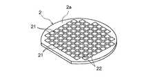
図1には、本発明に従って分割されるウエーハとしての半導体ウエーハの斜視図が示されている。図1に示す半導体ウエーハ2は、例えば厚さが300μmのシリコンウエーハからなっており、表面2aに複数の分割予定ライン21が格子状に形成されているとともに該複数の分割予定ライン21によって区画された複数の領域に回路22が形成されている。以下、この半導体ウエーハ2を個々の半導体チップに分割する分割方法について説明する。 FIG. 1 shows a perspective view of a semiconductor wafer as a wafer to be divided according to the present invention. The
半導体ウエーハ2を個々の半導体チップに分割するには、ウエーハに対して透過性を有するパルスレーザー光線を分割予定ラインに沿って照射し、該ウエーハの内部に分割予定ラインに沿って変質層を形成する変質層形成工程を実施する。この変質層形成工程は、図2乃至4に示すレーザー加工装置を用いて実施する。図2乃至図4に示すレーザー加工装置3は、被加工物を保持するチャックテーブル31と、該チャックテーブル31上に保持された被加工物にレーザー光線を照射するレーザー光線照射手段32と、チャックテーブル31上に保持された被加工物を撮像する撮像手段33を具備している。チャックテーブル31は、被加工物を吸引保持するように構成されており、図示しない移動機構によって図2において矢印Xで示す加工送り方向および矢印Yで示す割り出し送り方向に移動せしめられるようになっている。 In order to divide the
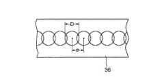
上記レーザー光線照射手段32は、実質上水平に配置された円筒形状のケーシング321を含んでいる。ケーシング321内には図3に示すようにパルスレーザー光線発振手段322と伝送光学系323とが配設されている。パルスレーザー光線発振手段322は、YAGレーザー発振器或いはYVO4レーザー発振器からなるパルスレーザー光線発振器322aと、これに付設された繰り返し周波数設定手段322bとから構成されている。伝送光学系323は、ビームスプリッタの如き適宜の光学要素を含んでいる。上記ケーシング321の先端部には、それ自体は周知の形態でよい組レンズから構成される集光レンズ(図示せず)を収容した集光器324が装着されている。上記パルスレーザー光線発振手段322から発振されたレーザー光線は、伝送光学系323を介して集光器324に至り、集光器324から上記チャックテーブル31に保持される被加工物に所定の集光スポット径Dで照射される。この集光スポット径Dは、図4に示すようにガウス分布を示すパルスレーザー光線が集光器324の対物レンズ324aを通して照射される場合、D(μm)=4×λ×f/(π×W)、ここでλはパルスレーザー光線の波長(μm)、Wは対物レンズ324aに入射されるパルスレーザー光線の直径(mm)、fは対物レンズ324aの焦点距離(mm)、で規定される。 The laser beam irradiation means 32 includes a
上記レーザー光線照射手段32を構成するケーシング321の先端部に装着された撮像手段33は、図示の実施形態においては可視光線によって撮像する通常の撮像素子(CCD)の外に、被加工物に赤外線を照射する赤外線照明手段と、該赤外線照明手段によって照射された赤外線を捕らえる光学系と、該光学系によって捕らえられた赤外線に対応した電気信号を出力する撮像素子(赤外線CCD)等で構成されており、撮像した画像信号を後述する制御手段に送る。 In the illustrated embodiment, the imaging means 33 mounted on the tip of the
上述したレーザー加工装置3を用いて実施する変質層形成工程について、図2、図5および図6を参照して説明する。
この変質層形成行程は、先ず上述した図2に示すレーザー加工装置3のチャックテーブル31上に半導体ウエーハ2を裏面2bを上にして載置し、該チャックテーブル31上に半導体ウエーハ2を吸着保持する。半導体ウエーハ2を吸引保持したチャックテーブル31は、図示しない移動機構によって撮像手段33の直下に位置付けられる。The deteriorated layer forming step performed using the
In this deteriorated layer forming step, first, the
チャックテーブル31が撮像手段33の直下に位置付けられると、撮像手段33および図示しない制御手段によって半導体ウエーハ2のレーザー加工すべき加工領域を検出するアライメント作業を実行する。即ち、撮像手段33および図示しない制御手段は、半導体ウエーハ2の所定方向に形成されている分割予定ライン21と、分割予定ライン21に沿ってレーザー光線を照射するレーザー光線照射手段32の集光器324との位置合わせを行うためのパターンマッチング等の画像処理を実行し、レーザー光線照射位置のアライメントを遂行する。また、半導体ウエーハ2に形成されている上記所定方向に対して直角に延びる分割予定ライン21に対しても、同様にレーザー光線照射位置のアライメントが遂行される。このとき、半導体ウエーハ2の分割予定ライン21が形成されている表面2aは下側に位置しているが、撮像手段33が上述したように赤外線照明手段と赤外線を捕らえる光学系および赤外線に対応した電気信号を出力する撮像素子(赤外線CCD)等で構成された撮像手段を備えているので、裏面2bから透かして分割予定ライン21を撮像することができる。 When the chuck table 31 is positioned immediately below the image pickup means 33, an alignment operation for detecting a processing region to be laser processed of the
以上のようにしてチャックテーブル31上に保持されている半導体ウエーハ2に形成されている分割予定ライン21を検出し、レーザー光線照射位置のアライメントが行われたならば、図5の(a)で示すようにチャックテーブル31をレーザー光線を照射するレーザー光線照射手段32の集光器324が位置するレーザー光線照射領域に移動し、所定の分割予定ライン21の一端(図5の(a)において左端)をレーザー光線照射手段32の集光器324の直下に位置付ける。そして、集光器324から透過性を有するパルスレーザー光線を照射しつつチャックテーブル31即ち半導体ウエーハ2を図5の(a)において矢印X1で示す方向に所定の送り速度で移動せしめる。そして、図5の(b)で示すようにレーザー光線照射手段32の集光器324の照射位置が分割予定ライン21の他端の位置に達したら、パルスレーザー光線の照射を停止するとともにチャックテーブル31即ち半導体ウエーハ2の移動を停止する。この変質層形成工程においては、パルスレーザー光線の集光点Pを半導体ウエーハ2の表面2a(下面)付近に合わせることにより、表面2a(下面)に露出するとともに表面2aから内部に向けて変質層210が形成される。この変質層210は、溶融再固化層として形成される。 If the
なお、上記変質層形成工程における加工条件は、例えば次のように設定されている。
光源 ;LD励起QスイッチNd:YVO4スレーザー
波長 ;1064nmのパルスレーザー
パルス出力 :10μJ
集光スポット径 ;φ1μm
パルス幅 ;100ns
集光点のピークパワー密度;1.3×10¹⁰W/cm2
繰り返し周波数 :200〜400kHz
加工送り速度 ;200〜400mm/秒Note that the processing conditions in the deteriorated layer forming step are set as follows, for example.
Light source: LD excitation Q switch Nd: YVO4 laser wavelength: 1064 nm pulse laser Pulse output: 10 μJ
Condensing spot diameter: φ1μm
Pulse width: 100 ns
Peak power density at the focal point; 1.3 × 10¹⁰ W / cm2
Repetition frequency: 200 to 400 kHz
Processing feed rate: 200 to 400 mm / sec
なお、半導体ウエーハ2の厚さが厚い場合には、図6に示すように集光点Pを段階的に変えて上述した変質層形成工程を複数回実行することにより、複数の変質層210を形成する。なお、上述した加工条件においては1回に形成される変質層の厚さは約50μmであるため、図示の実施形態においては厚さが300μmのウエーハ2に対して6層の変質層を形成する。この結果、半導体ウエーハ2の内部に形成される変質層210は、分割予定ライン21に沿って表面2aから裏面2bに渡って形成される。 When the thickness of the
上記加工条件においては、パルスレーザー光線の繰り返し周波数Y(Hz)、パルスレーザー光線の、集光スポット径D(mm)、加工送り速度V(mm/秒)によって規定される係数k、k=V/(Y×D)を1.0乃至2.5に設定することが望ましい。換言すれば、繰り返し周波数Y、集光スポット径Dおよび加工送り速度Vの関係を、1.0≦V/(Y×D)≦2.5に設定することが望ましい。
Under the above processing conditions, the coefficient k defined by the repetition frequency Y (Hz) of the pulse laser beam, the focused spot diameter D (mm) of the pulse laser beam, and the processing feed rate V (mm / second), k = V / ( It is desirable to set Y × D) to 1.0 to 2.5. In other words, it is desirable to set the relationship of the repetition frequency Y, the focused spot diameter D, and the processing feed speed V to 1.0 ≦ V / (Y × D) ≦ 2.5.
更に詳述すると、レーザー光線照射手段32の集光器324から繰り返し周波数Yのパルスレーザー光線を集光スポット径Dで半導体ウエーハ2に照射し、チャックテーブル31即ち半導体ウエーハ2を加工送りする場合、上記係数kが1である場合には図7に示すようにパルスレーザー光線のスポットのピッチpは集光スポット径Dと同一、従ってパルスレーザー光線を集光スポットは相互の接した状態(即ち互いに重なり合うことがなく且つ隣接するスポット間に隙間が生じない状態)で、分割予定ライン21に沿って連続して照射されることになる。また、上記係数kが1未満になると、図8に示すようにパルスレーザー光線のスポットは相互に重なり合って、分割予定ライン21に沿って連続して照射されることになる。一方、上記係数kが1より大きくなると図9に示すようにパルスレーザー光線のスポットは隣接するスポット間に隙間を設けて、分割予定ライン21に沿って連続して照射されることになり、上記係数kが2になると隣接するスポット間の間隔sは集光スポット径Dと同じ長さとなる。 More specifically, when the
実験例
直径が6インチで厚さが300μmの半導体ウエーハに上述した加工条件で上記係数kを0.1から4.0の変位に変化させて上記変質層を形成し、それぞれの場合に分割予定ラインに沿って半導体ウエーハを破断するために要した応力を測定した。応力測定の際には、半導体ウエーハの裏面を分割予定ラインから両側に2.0mm離れた部位に分割予定ラインに沿って支持し、半導体ウエーハの表面に分割予定ラインに沿って荷重を加える三点曲げ試験を実施し、測定された応力は半導体ウエーハが破断した時の荷重に基づいた断面における応力である。測定結果は図10に示すとおりであり、係数kが1.0〜2.5の場合には半導体ウエーハを破断するのに要する応力が小さいことが判る。Experimental Example A semiconductor wafer having a diameter of 6 inches and a thickness of 300 μm is formed by changing the coefficient k from 0.1 to 4.0 under the above-described processing conditions to form the deteriorated layer, and to be divided in each case. The stress required to break the semiconductor wafer along the line was measured. When measuring stress, the back side of the semiconductor wafer is supported along the planned dividing line at a location 2.0 mm away from the planned dividing line on both sides, and a load is applied to the surface of the semiconductor wafer along the planned dividing line. The stress measured in the bending test is the stress in the cross section based on the load when the semiconductor wafer is broken. The measurement results are as shown in FIG. 10, and it can be seen that the stress required to break the semiconductor wafer is small when the coefficient k is 1.0 to 2.5.
上述した変質層形成工程によって半導体ウエーハ2の内部に分割予定ライン21に沿って変質層210を形成したならば、ウエーハの一方の面に拡張可能な保護テープを貼着する保護テープ貼着工程を実施する。即ち、図11に示すように環状のダイシングフレーム41の内側開口部を覆うように外周部が装着された伸長可能な保護テープ42の表面を半導体ウエーハ2の裏面2bに貼着する。なお、上記保護テープ42は、図示の実施形態においては厚さが70μmのポリ塩化ビニル(PVC)からなるシート基材の表面にアクリル樹脂系の糊が厚さが5μm程度塗布されている。この糊は紫外線等の外的刺激によって粘着力が低下する性質を有するものが用いられている。なお、保護テープ貼着工程は、上述した変質層形成工程を実施する前に実施してもよい。即ち、半導体ウエーハ2の裏面2bを上側にして表面2aにして保護テープ42に貼着し、ダイシングフレーム41に支持された状態で変質層形成工程を実施する。 If the deteriorated
上述した変質層形成工程および保護テープ貼着工程を実施したならば、半導体ウエーハ2に貼着された保護テープ42を伸長することにより半導体ウエーハ2を変質層210に沿って分割する分割工程を実施する。この分割工程は、図12および図13に示すピックアップ装置5によって実施される。ここで、ピックアップ装置5について説明する。図示のピックアップ装置5は、上記ダイシングフレーム41を載置する載置面511が形成された円筒状のベース51と、該ベース51内に同心的に配設されダイシングフレーム41に装着された保護テープ42を押し広げるための拡張手段52を具備している。拡張手段52は、上記保護テープ42における半導体ウエーハ2が存在する領域421を支持する筒状の拡張部材521を具備している。この拡張部材521は、図示しない昇降手段によって図13の(a)に示す基準位置と該基準位置から上方の図13の(b)に示す拡張位置の間を上下方向(円筒状のベース51の軸方向)に移動可能に構成されている。なお、図示の実施形態においては拡張部材521内には、紫外線照射ランプ53が配設されている。 After performing the above-described deteriorated layer forming step and protective tape attaching step, the dividing step of dividing the
上述したピックアップ装置5を用いて実施する分割工程について、図12および図13を参照して説明する。
上述したように半導体ウエーハ2の裏面に貼着された保護テープ42を装着したダイシングフレーム41は、図12および図13の(a)に示すように円筒状のベース51の載置面511上に載置され、クランプ54によってベース51に固定される。次に、図13の(b)に示すように上記保護テープ42における半導体ウエーハ2が存在する領域421を支持した拡張手段52の拡張部材521を図示しない昇降手段によって図13(a)の基準位置から上方の図13の(b)に示す拡張位置まで移動する。この結果、伸長可能な保護テープ42は拡張されるので、保護テープ42が貼着されている半導体ウエーハ2は放射状に引張力が作用する。このように半導体ウエーハ2に放射状に引張力が作用すると、分割予定ラインに沿って形成された変質層210は強度が低下せしめられているので、半導体ウエーハ2は変質層210に沿って破断され個々の半導体チップ20に分割される。なお、上記分割工程における保護テープ42の拡張量即ち伸び量は拡張部材521の上方への移動量によって調整することができ、本発明者等の実験によると保護テープ42を20mm程度を引き伸ばしたときに半導体ウエーハ2を変質層210に沿って破断することができた。The dividing process performed using the
As described above, the dicing
実験例
直径が6インチで厚さが300μmの半導体ウエーハ(シリコンウエーハ)を上述した方法によって2mm×2mmの半導体チップに分割した。このとき、上記変質層形成工程において照射するパルスレーザー光線の繰り返し周波数を100kHz、150kHz、200kHz、300kHz、400kHzとした場合(なお、上記係数kは1で実施した)に、上述した分割工程(以下、テープエキスパンド法という)を実施することにより半導体ウエーハが変質層に沿って破断され分割された半導体チップの割合を示したのが図15である。図15において横軸は上記変質層形成工程において照射するパルスレーザー光線の繰り返し周波数、縦軸は上記半導体ウエーハが上述したテープエキスパンド法を実施することにより個々の半導体チップに分割された個数を上記半導体ウエーハに形成された半導体チップの個数で除算した値に100を乗算したチップ化率である。Experimental Example A semiconductor wafer (silicon wafer) having a diameter of 6 inches and a thickness of 300 μm was divided into 2 mm × 2 mm semiconductor chips by the method described above. At this time, when the repetition frequency of the pulse laser beam irradiated in the deteriorated layer forming step is 100 kHz, 150 kHz, 200 kHz, 300 kHz, 400 kHz (note that the coefficient k is 1), the above-described dividing step (hereinafter, FIG. 15 shows the ratio of the semiconductor chips in which the semiconductor wafer is broken and divided along the deteriorated layer by performing the tape expanding method). In FIG. 15, the horizontal axis represents the repetition frequency of the pulse laser beam irradiated in the deteriorated layer forming step, and the vertical axis represents the number of the semiconductor wafer divided into individual semiconductor chips by performing the tape expanding method described above. The chip ratio is obtained by multiplying the value divided by the number of semiconductor chips formed in 100 by 100.
図15から判るように、上記変質層形成工程において照射するパルスレーザー光線の繰り返し周波数が100kHzの場合には、上述したテープエキスパンド法によって約半分しかチップ化されず、残りの約半分はチップ化されない。このチップ化されないものに対して保護テープ42の引張力を増加したが変質層が破断することはなかったが、変質層に曲げ荷重を作用せしめ曲げ応力を発生させると容易に破断した。また、上記変質層形成工程において照射するパルスレーザー光線の繰り返し周波数が150kHzの場合には、上述したテープエキスパンド法によって95%がチップ化された。これに対して上記変質層形成工程において照射するパルスレーザー光線の繰り返し周波数が200kHz以上になると、チップ化率が100%に達することが判る。 As can be seen from FIG. 15, when the repetition frequency of the pulse laser beam applied in the deteriorated layer forming step is 100 kHz, only about half is formed by the tape expanding method, and the remaining about half is not formed. Although the tensile force of the
次に、上記変質層形成工程において照射するパルスレーザー光線の繰り返し周波数が150kHz以下の場合にチップ化率が低下した理由について検討する。なお、上記各繰り返し周波数のパルスレーザー光線を照射して形成した変質層の破断面を観察したが、いずれも半導体チップの厚さ方向全域に変質層が形成されていた。これを確認したのは、変質層が形成されていない部分が存在すると、分割に必要な応力が著しく大きくなるため、これが起因してチップ化率が低下する可能性があるためである。
図16は、三点曲げ試験法により上記変質層を破断するのに必要な曲げ応力を測定した試験結果であり、横軸は変質層を形成したパルスレーザー光線の繰り返し周波数(kHz)、縦軸は変質層を破断するのに必要な曲げ応力(MPa)である。図16から判るように変質層を形成するパルスレーザー光線の繰り返し周波数が150kHz以下では変質層を破断するのに必要な曲げ応力が増大していくが、変質層を形成するパルスレーザー光線の繰り返し周波数が200kHz以上では変質層を破断するのに必要な曲げ応力が2MPa以下となる。なお、変質層を破断するのに必要な応力と上述したテープエキスパンド法によるチップ化率には関係があり、応力が大きいほどテープエキスパンド法によるチップ化率は低下するが、所定の応力以下になればテープエキスパンド法によるチップ化率は100%となる。従って、上記変質層形成工程において照射するパルスレーザー光線の繰り返し周波数は、200kHz以上に設定することが望ましい。Next, the reason why the chip formation rate is reduced when the repetition frequency of the pulse laser beam irradiated in the deteriorated layer forming step is 150 kHz or less will be examined. In addition, although the fracture surface of the deteriorated layer formed by irradiating the pulse laser beam of each said repetition frequency was observed, all had the deteriorated layer formed in the whole thickness direction of a semiconductor chip. This is confirmed because if there is a portion where the deteriorated layer is not formed, the stress required for the division becomes remarkably large, which may reduce the chip formation rate.
FIG. 16 shows the test results obtained by measuring the bending stress necessary for breaking the above-mentioned deteriorated layer by the three-point bending test method, where the horizontal axis represents the repetition frequency (kHz) of the pulse laser beam that formed the deteriorated layer, and the vertical axis represents It is a bending stress (MPa) necessary for breaking the deteriorated layer. As can be seen from FIG. 16, when the repetition frequency of the pulsed laser beam for forming the deteriorated layer is 150 kHz or less, the bending stress required to break the deteriorated layer increases, but the repetition frequency of the pulsed laser beam for forming the deteriorated layer is 200 kHz. As described above, the bending stress necessary for breaking the deteriorated layer is 2 MPa or less. There is a relationship between the stress required to break the damaged layer and the above-mentioned chip expansion rate by the tape expanding method. The higher the stress, the lower the chip forming rate by the tape expanding method, but it is below the predetermined stress. For example, the chip formation rate by the tape expanding method is 100%. Therefore, it is desirable to set the repetition frequency of the pulse laser beam irradiated in the deteriorated layer forming step to 200 kHz or more.
上述したようにテープエキスパンド法による分割工程を実施することにより、ダイシングテープ62と半導体チップ20との間にズレが生じ密着性が低下するため、半導体チップ20が保護テープ42から容易に離脱できる状態となるとともに、図13の(b)に示すように個々の半導体チップ20間には隙間は形成される。 As described above, by performing the dividing process by the tape expanding method, a gap is generated between the dicing tape 62 and the
次に、図12に示すようにピックアップ装置5の上方に配置されたピックアップコレット6を作動して、個々の半導体チップ20を保護テープ42の上面から離脱し、図示しないトレーに搬送する。このとき、拡張部材521内に配設された紫外線照射ランプ53を点灯して保護テープ42に紫外線を照射し、保護テープ42の粘着力を低下せしめることにより、より容易に離脱することができる。このようにして、保護テープ42から離脱された半導体チップ20は、図14に示すように半導体チップ20が得られる。 Next, as shown in FIG. 12, the pickup collet 6 disposed above the
2:半導体ウエーハ
20:半導体チップ
21:分割予定ライン
22:回路
210:変質層
3:レーザー加工装置
31:レーザー加工装置のチャックテーブル
31:レーザー光線照射手段
33:撮像手段
41:ダイシングフレーム
4:保護テープ
5:ピックアップ装置
51:円筒状のベース
52:拡張手段
521:拡張部材
53:紫外線照射ランプ
6:ピックアップコレット2: Semiconductor wafer 20: Semiconductor chip 21: Divided line 22: Circuit 210: Altered layer 3: Laser processing device 31: Chuck table of laser processing device 31: Laser beam irradiation means 33: Imaging means 41: Dicing frame 4: Protective tape 5: Pickup device 51: Cylindrical base 52: Expansion means 521: Expansion member 53: Ultraviolet irradiation lamp 6: Pickup collet
Claims (6)
Translated fromJapanese該ウエーハに対して透過性を有するパルスレーザー光線を該分割予定ラインに沿って照射し、該ウエーハの内部に該分割予定ラインに沿って変質層を形成する変質層形成工程と、
該変質層形成工程を実施する前または該変質層形成工程を実施した後に、該ウエーハの一方の面に伸長可能な保護テープを貼着する保護テープ貼着工程と、
該変質層形成工程を実施した後に、該ウエーハに貼着された保護テープを拡張することにより該ウエーハを該変質層に沿って分割する分割工程と、を含む、
ことを特徴とするウエーハの分割方法。A wafer processing method for dividing a wafer along a predetermined division line,
A deteriorated layer forming step of irradiating a pulse laser beam having transparency to the wafer along the division line and forming a deteriorated layer along the division line inside the wafer;
A protective tape attaching step for attaching an extensible protective tape to one surface of the wafer before the altered layer forming step or after the altered layer forming step;
A step of dividing the wafer along the deteriorated layer by expanding the protective tape attached to the wafer after performing the deteriorated layer forming step.
A wafer dividing method characterized by the above.
Priority Applications (4)
| Application Number | Priority Date | Filing Date | Title |
|---|---|---|---|
| JP2003361471AJP2005129607A (en) | 2003-10-22 | 2003-10-22 | Wafer division method |
| US10/968,100US7232741B2 (en) | 2003-10-22 | 2004-10-20 | Wafer dividing method |
| DE102004051180ADE102004051180B4 (en) | 2003-10-22 | 2004-10-20 | Wafer dividing method |
| CNB2004100870487ACN100444326C (en) | 2003-10-22 | 2004-10-22 | Wafer Separation Method |
Applications Claiming Priority (1)
| Application Number | Priority Date | Filing Date | Title |
|---|---|---|---|
| JP2003361471AJP2005129607A (en) | 2003-10-22 | 2003-10-22 | Wafer division method |
Publications (1)
| Publication Number | Publication Date |
|---|---|
| JP2005129607Atrue JP2005129607A (en) | 2005-05-19 |
Family
ID=34509940
Family Applications (1)
| Application Number | Title | Priority Date | Filing Date |
|---|---|---|---|
| JP2003361471APendingJP2005129607A (en) | 2003-10-22 | 2003-10-22 | Wafer division method |
Country Status (4)
| Country | Link |
|---|---|
| US (1) | US7232741B2 (en) |
| JP (1) | JP2005129607A (en) |
| CN (1) | CN100444326C (en) |
| DE (1) | DE102004051180B4 (en) |
Cited By (26)
| Publication number | Priority date | Publication date | Assignee | Title |
|---|---|---|---|---|
| JP2006120797A (en)* | 2004-10-20 | 2006-05-11 | Disco Abrasive Syst Ltd | Wafer divider |
| JP2007019159A (en)* | 2005-07-06 | 2007-01-25 | Disco Abrasive Syst Ltd | Wafer divider |
| JP2007142002A (en)* | 2005-11-16 | 2007-06-07 | Denso Corp | Semiconductor wafer pressing tool and usage thereof |
| JP2007150206A (en)* | 2005-11-30 | 2007-06-14 | Furukawa Electric Co Ltd:The | Dicing tape |
| US7329564B2 (en) | 2004-08-10 | 2008-02-12 | Disco Corporation | Wafer dividing method |
| US7341926B2 (en) | 2005-03-01 | 2008-03-11 | Disco Corporation | Wafer dividing method |
| US7348199B2 (en) | 2004-07-07 | 2008-03-25 | Disco Corporation | Wafer dividing method |
| US7350446B2 (en) | 2004-10-26 | 2008-04-01 | Disco Corporation | Wafer dividing apparatus |
| US7446020B2 (en) | 2004-10-04 | 2008-11-04 | Disco Corporation | Wafer dividing method and dividing apparatus |
| DE112007000608T5 (en) | 2006-03-14 | 2009-01-15 | Hamamatsu Photonics K.K., Hamamatsu | Laser processing and laser processing system |
| US7754583B2 (en) | 2005-11-18 | 2010-07-13 | Hamamatsu Photonics K.K. | Laser processing method |
| CN102248608A (en)* | 2010-05-19 | 2011-11-23 | 株式会社迪思科 | Plate object dividing device |
| US8415234B2 (en) | 2011-05-12 | 2013-04-09 | Disco Corporation | Wafer dividing method |
| JP2013105823A (en)* | 2011-11-11 | 2013-05-30 | Disco Abrasive Syst Ltd | Method for dividing plate-like object |
| JP2013149900A (en)* | 2012-01-23 | 2013-08-01 | Disco Abrasive Syst Ltd | Workpiece division method |
| US8642920B2 (en) | 2009-12-18 | 2014-02-04 | Disco Corporation | Wafer dividing apparatus and laser processing apparatus |
| DE102005014740B4 (en)* | 2004-03-31 | 2014-11-27 | Disco Corporation | Band expander |
| CN104439711A (en)* | 2013-09-17 | 2015-03-25 | 上海华虹集成电路有限责任公司 | Laser scribing method reducing chip physical stress damage |
| CN109003897A (en)* | 2017-06-07 | 2018-12-14 | 株式会社迪思科 | The dividing method and segmenting device of chip |
| DE102018220595A1 (en) | 2017-11-30 | 2019-06-06 | Disco Corporation | Laser processing method for a wafer |
| KR20190064440A (en) | 2017-11-30 | 2019-06-10 | 가부시기가이샤 디스코 | Wafer dividing method and wafer dividing apparatus |
| DE102019200462A1 (en) | 2018-01-16 | 2019-07-18 | Disco Corporation | METHOD FOR WORKING A WORKPIECE WITH A LASER BEAM |
| DE102019216642A1 (en) | 2018-10-30 | 2020-04-30 | Disco Corporation | WAFER EXPANSION METHOD AND WAFER EXPANSION DEVICE |
| DE102019216640A1 (en) | 2018-10-30 | 2020-04-30 | Disco Corporation | WAFER EXPANSION METHOD AND WAFER EXPANSION DEVICE |
| KR20210070212A (en) | 2019-12-04 | 2021-06-14 | 가부시기가이샤 디스코 | Laser machining method |
| KR20230149733A (en) | 2022-04-20 | 2023-10-27 | 가부시기가이샤 디스코 | Holding unit |
Families Citing this family (21)
| Publication number | Priority date | Publication date | Assignee | Title |
|---|---|---|---|---|
| JP2005203541A (en)* | 2004-01-15 | 2005-07-28 | Disco Abrasive Syst Ltd | Wafer laser processing method |
| JP4447392B2 (en)* | 2004-07-23 | 2010-04-07 | 株式会社ディスコ | Wafer dividing method and dividing apparatus |
| JP2006114691A (en)* | 2004-10-14 | 2006-04-27 | Disco Abrasive Syst Ltd | Wafer division method |
| JP2006269897A (en)* | 2005-03-25 | 2006-10-05 | Disco Abrasive Syst Ltd | Wafer laser processing method |
| JP4749851B2 (en)* | 2005-11-29 | 2011-08-17 | 株式会社ディスコ | Wafer dividing method |
| JP2007242787A (en)* | 2006-03-07 | 2007-09-20 | Disco Abrasive Syst Ltd | Wafer division method |
| US20070272666A1 (en)* | 2006-05-25 | 2007-11-29 | O'brien James N | Infrared laser wafer scribing using short pulses |
| JP4480728B2 (en)* | 2006-06-09 | 2010-06-16 | パナソニック株式会社 | Method for manufacturing MEMS microphone |
| JP2008227276A (en)* | 2007-03-14 | 2008-09-25 | Disco Abrasive Syst Ltd | Wafer division method |
| DE102007012815B4 (en) | 2007-03-16 | 2024-06-06 | Dmg Mori Ultrasonic Lasertec Gmbh | Method and device for forming a die |
| CN102308372A (en) | 2008-12-05 | 2012-01-04 | 新加坡科技研究局 | A wafer cutting method and a system thereof |
| US9701581B2 (en)* | 2009-06-04 | 2017-07-11 | Corelase Oy | Method and apparatus for processing substrates using a laser |
| US7977213B1 (en)* | 2010-03-31 | 2011-07-12 | Electro Scientific Industries, Inc. | Use of laser energy transparent stop layer to achieve minimal debris generation in laser scribing a multilayer patterned workpiece |
| FI125379B (en)* | 2010-10-25 | 2015-09-15 | Jot Automation Oy | Chassis |
| JP5480169B2 (en) | 2011-01-13 | 2014-04-23 | 浜松ホトニクス株式会社 | Laser processing method |
| JP2012238746A (en)* | 2011-05-12 | 2012-12-06 | Disco Abrasive Syst Ltd | Division method of optical device wafer |
| CN106467289B (en)* | 2015-08-20 | 2020-09-18 | 共达电声股份有限公司 | Wafer structure and wafer processing method |
| JP2017168736A (en)* | 2016-03-17 | 2017-09-21 | 株式会社ディスコ | Wafer processing method |
| JP6979296B2 (en)* | 2017-07-28 | 2021-12-08 | 株式会社ディスコ | Cutting method |
| CN110165008B (en)* | 2018-02-11 | 2023-04-25 | 苏州沃特维自动化系统有限公司 | Solar cell connection method |
| CN109175726A (en)* | 2018-09-18 | 2019-01-11 | 苏州斯尔特微电子有限公司 | A kind of automation wafer cutting and positioning device |
Family Cites Families (9)
| Publication number | Priority date | Publication date | Assignee | Title |
|---|---|---|---|---|
| JP3455102B2 (en)* | 1998-02-06 | 2003-10-14 | 三菱電機株式会社 | Semiconductor wafer chip separation method |
| US6451152B1 (en)* | 2000-05-24 | 2002-09-17 | The Boeing Company | Method for heating and controlling temperature of composite material during automated placement |
| JP4659300B2 (en) | 2000-09-13 | 2011-03-30 | 浜松ホトニクス株式会社 | Laser processing method and semiconductor chip manufacturing method |
| JP3626442B2 (en)* | 2000-09-13 | 2005-03-09 | 浜松ホトニクス株式会社 | Laser processing method |
| JP2003019583A (en)* | 2000-09-13 | 2003-01-21 | Hamamatsu Photonics Kk | Method for laser beam machining |
| JP3612317B2 (en)* | 2001-11-30 | 2005-01-19 | 株式会社東芝 | Manufacturing method of semiconductor device |
| JP2004111601A (en)* | 2002-09-18 | 2004-04-08 | Tokyo Seimitsu Co Ltd | Die bonder |
| JP4494728B2 (en)* | 2003-05-26 | 2010-06-30 | 株式会社ディスコ | Non-metallic substrate division method |
| US20050064683A1 (en)* | 2003-09-19 | 2005-03-24 | Farnworth Warren M. | Method and apparatus for supporting wafers for die singulation and subsequent handling |
- 2003
- 2003-10-22JPJP2003361471Apatent/JP2005129607A/enactivePending
- 2004
- 2004-10-20DEDE102004051180Apatent/DE102004051180B4/ennot_activeExpired - Lifetime
- 2004-10-20USUS10/968,100patent/US7232741B2/ennot_activeExpired - Lifetime
- 2004-10-22CNCNB2004100870487Apatent/CN100444326C/ennot_activeExpired - Lifetime
Cited By (38)
| Publication number | Priority date | Publication date | Assignee | Title |
|---|---|---|---|---|
| DE102005014740B4 (en)* | 2004-03-31 | 2014-11-27 | Disco Corporation | Band expander |
| US7348199B2 (en) | 2004-07-07 | 2008-03-25 | Disco Corporation | Wafer dividing method |
| US7329564B2 (en) | 2004-08-10 | 2008-02-12 | Disco Corporation | Wafer dividing method |
| US7446020B2 (en) | 2004-10-04 | 2008-11-04 | Disco Corporation | Wafer dividing method and dividing apparatus |
| US7497213B2 (en) | 2004-10-20 | 2009-03-03 | Disco Corporation | Wafer dividing apparatus |
| JP2006120797A (en)* | 2004-10-20 | 2006-05-11 | Disco Abrasive Syst Ltd | Wafer divider |
| US7350446B2 (en) | 2004-10-26 | 2008-04-01 | Disco Corporation | Wafer dividing apparatus |
| US7341926B2 (en) | 2005-03-01 | 2008-03-11 | Disco Corporation | Wafer dividing method |
| JP2007019159A (en)* | 2005-07-06 | 2007-01-25 | Disco Abrasive Syst Ltd | Wafer divider |
| JP2007142002A (en)* | 2005-11-16 | 2007-06-07 | Denso Corp | Semiconductor wafer pressing tool and usage thereof |
| US8124500B2 (en) | 2005-11-18 | 2012-02-28 | Hamamatsu Photonics K.K. | Laser processing method |
| US7754583B2 (en) | 2005-11-18 | 2010-07-13 | Hamamatsu Photonics K.K. | Laser processing method |
| JP2007150206A (en)* | 2005-11-30 | 2007-06-14 | Furukawa Electric Co Ltd:The | Dicing tape |
| US8890027B2 (en) | 2006-03-14 | 2014-11-18 | Hamamatsu Photonics K.K. | Laser processing method and laser processing system |
| DE112007000608T5 (en) | 2006-03-14 | 2009-01-15 | Hamamatsu Photonics K.K., Hamamatsu | Laser processing and laser processing system |
| US8642920B2 (en) | 2009-12-18 | 2014-02-04 | Disco Corporation | Wafer dividing apparatus and laser processing apparatus |
| CN102248608A (en)* | 2010-05-19 | 2011-11-23 | 株式会社迪思科 | Plate object dividing device |
| US8415234B2 (en) | 2011-05-12 | 2013-04-09 | Disco Corporation | Wafer dividing method |
| JP2013105823A (en)* | 2011-11-11 | 2013-05-30 | Disco Abrasive Syst Ltd | Method for dividing plate-like object |
| JP2013149900A (en)* | 2012-01-23 | 2013-08-01 | Disco Abrasive Syst Ltd | Workpiece division method |
| CN104439711A (en)* | 2013-09-17 | 2015-03-25 | 上海华虹集成电路有限责任公司 | Laser scribing method reducing chip physical stress damage |
| CN109003897A (en)* | 2017-06-07 | 2018-12-14 | 株式会社迪思科 | The dividing method and segmenting device of chip |
| KR20180133789A (en) | 2017-06-07 | 2018-12-17 | 가부시기가이샤 디스코 | Wafer dividing method and wafer dividing apparatus |
| CN109003897B (en)* | 2017-06-07 | 2023-08-01 | 株式会社迪思科 | Wafer dividing method and dividing device |
| US10559487B2 (en) | 2017-06-07 | 2020-02-11 | Disco Corporation | Wafer dividing method and dividing apparatus |
| DE102018220595A1 (en) | 2017-11-30 | 2019-06-06 | Disco Corporation | Laser processing method for a wafer |
| KR20190064434A (en) | 2017-11-30 | 2019-06-10 | 가부시기가이샤 디스코 | Laser machining method of wafer |
| KR20190064440A (en) | 2017-11-30 | 2019-06-10 | 가부시기가이샤 디스코 | Wafer dividing method and wafer dividing apparatus |
| DE102018220595B4 (en) | 2017-11-30 | 2021-07-15 | Disco Corporation | Laser processing method for a wafer |
| US10573559B2 (en) | 2017-11-30 | 2020-02-25 | Disco Corporation | Laser processing method for wafer |
| DE102019200462A1 (en) | 2018-01-16 | 2019-07-18 | Disco Corporation | METHOD FOR WORKING A WORKPIECE WITH A LASER BEAM |
| KR20190087288A (en) | 2018-01-16 | 2019-07-24 | 가부시기가이샤 디스코 | Laser machining method of workpiece to be processed |
| DE102019216640A1 (en) | 2018-10-30 | 2020-04-30 | Disco Corporation | WAFER EXPANSION METHOD AND WAFER EXPANSION DEVICE |
| DE102019216642A1 (en) | 2018-10-30 | 2020-04-30 | Disco Corporation | WAFER EXPANSION METHOD AND WAFER EXPANSION DEVICE |
| DE102019216640B4 (en) | 2018-10-30 | 2023-01-26 | Disco Corporation | WAFER EXPANSION PROCESS |
| KR20210070212A (en) | 2019-12-04 | 2021-06-14 | 가부시기가이샤 디스코 | Laser machining method |
| KR20230149733A (en) | 2022-04-20 | 2023-10-27 | 가부시기가이샤 디스코 | Holding unit |
| US12330251B2 (en) | 2022-04-20 | 2025-06-17 | Disco Corporation | Holding unit |
Also Published As
| Publication number | Publication date |
|---|---|
| DE102004051180B4 (en) | 2011-02-24 |
| DE102004051180A1 (en) | 2005-07-07 |
| CN1612304A (en) | 2005-05-04 |
| US7232741B2 (en) | 2007-06-19 |
| US20050090077A1 (en) | 2005-04-28 |
| CN100444326C (en) | 2008-12-17 |
Similar Documents
| Publication | Publication Date | Title |
|---|---|---|
| JP2005129607A (en) | Wafer division method | |
| JP4733934B2 (en) | Wafer processing method | |
| JP4769560B2 (en) | Wafer division method | |
| JP4694795B2 (en) | Wafer division method | |
| JP2005135964A (en) | Wafer division method | |
| JP2006114691A (en) | Wafer division method | |
| JP2006054246A (en) | Wafer separation method | |
| JP2005086161A (en) | Wafer processing method | |
| JP5992731B2 (en) | Wafer processing method | |
| JP2007173475A (en) | Wafer division method | |
| JP2009200140A (en) | Method of manufacturing semiconductor chip | |
| JP2008294191A (en) | Wafer division method | |
| JP2006229021A (en) | Wafer division method | |
| JP2011003757A (en) | Method of dividing wafer | |
| JP4447392B2 (en) | Wafer dividing method and dividing apparatus | |
| JP2007157887A (en) | Wafer division method | |
| JP2008042110A (en) | Wafer division method | |
| JP4471627B2 (en) | Wafer division method | |
| JP4630689B2 (en) | Wafer division method | |
| JP4402974B2 (en) | Wafer division method | |
| JP2006202933A (en) | Wafer division method | |
| JP2008227276A (en) | Wafer division method | |
| JP2006024676A (en) | Wafer division method | |
| JP2015023135A (en) | Wafer processing method | |
| JP2005223283A (en) | Wafer division method |
Legal Events
| Date | Code | Title | Description |
|---|---|---|---|
| A621 | Written request for application examination | Free format text:JAPANESE INTERMEDIATE CODE: A621 Effective date:20060712 | |
| A977 | Report on retrieval | Free format text:JAPANESE INTERMEDIATE CODE: A971007 Effective date:20090423 | |
| A131 | Notification of reasons for refusal | Free format text:JAPANESE INTERMEDIATE CODE: A131 Effective date:20090428 | |
| A521 | Request for written amendment filed | Free format text:JAPANESE INTERMEDIATE CODE: A523 Effective date:20090624 | |
| A02 | Decision of refusal | Free format text:JAPANESE INTERMEDIATE CODE: A02 Effective date:20100223 |