JP2005123506A - Semiconductor device - Google Patents
Semiconductor deviceDownload PDFInfo
- Publication number
- JP2005123506A JP2005123506AJP2003359106AJP2003359106AJP2005123506AJP 2005123506 AJP2005123506 AJP 2005123506AJP 2003359106 AJP2003359106 AJP 2003359106AJP 2003359106 AJP2003359106 AJP 2003359106AJP 2005123506 AJP2005123506 AJP 2005123506A
- Authority
- JP
- Japan
- Prior art keywords
- electrical connection
- same
- connection
- semiconductor device
- rows
- Prior art date
- Legal status (The legal status is an assumption and is not a legal conclusion. Google has not performed a legal analysis and makes no representation as to the accuracy of the status listed.)
- Withdrawn
Links
Images


Landscapes
- Solid State Image Pick-Up Elements (AREA)
- Light Receiving Elements (AREA)
Abstract
Translated fromJapaneseDescription
Translated fromJapanese本発明は、半導体装置に関り、例えば、大面積プロセスを用いて形成する液晶テレビ・液晶プロジェクター等の薄膜トランジスタを用いた表示装置やファクシミリ・デジタルコピー機、あるいはX線撮像装置等の放射線検出装置等に係る半導体装置に関する。 The present invention relates to a semiconductor device, for example, a display device using a thin film transistor such as a liquid crystal television and a liquid crystal projector formed by using a large area process, a radiation detection device such as a facsimile and digital copier, or an X-ray imaging device. And the like.
従来、ファクシミリや複写機、スキャナあるいはX線撮像装置等の読み取り装置として、縮小光学系とCCD型センサーを組み合わせたシステムがあった。しかしながら、近年になり水素化アモルファスシリコン(以下a−Siと記す)に代表される光電変換半導体材料の開発により、光電変換素子及び信号処理部を大面積の基板に形成し、情報源と等倍の光学系で読み取る密着型センサーの開発が進んでいる。 Conventionally, there has been a system that combines a reduction optical system and a CCD sensor as a reading device such as a facsimile, a copying machine, a scanner, or an X-ray imaging device. However, in recent years, with the development of photoelectric conversion semiconductor materials typified by hydrogenated amorphous silicon (hereinafter referred to as a-Si), photoelectric conversion elements and signal processing parts are formed on a large-area substrate, and the same size as the information source. Development of contact-type sensors that can be read by optical systems is progressing.
特にa−Siは光電変換材料としてだけでなく、薄膜電界効果型トランジスタ(以下TFTと記す)の半導体材料としても用いることができるので光電変換半導体層とTFTの半導体層と同時に形成することができる利点を有している。 In particular, a-Si can be used not only as a photoelectric conversion material but also as a semiconductor material of a thin film field effect transistor (hereinafter referred to as TFT), and therefore can be formed simultaneously with the photoelectric conversion semiconductor layer and the semiconductor layer of the TFT. Has advantages.
以下、従来技術について図を用いて説明する。 Hereinafter, the prior art will be described with reference to the drawings.
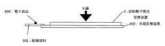
図3(A)(B)は従来の半導体装置としての一例として放射線撮像装置の概略の構成を示した図であり、図3(A)は模式的平面図、図3(B)は図3(A)のA−−−A′の模式的断面図である。 3A and 3B are diagrams showing a schematic configuration of a radiation imaging apparatus as an example of a conventional semiconductor device, FIG. 3A is a schematic plan view, and FIG. 3B is FIG. It is typical sectional drawing of A --- A 'of (A).
図3(A)(B)において、半導体基板である光電変換装置300は、ガラス等からなる基板1上の画素領域に画素が二次元的に配列されており、画素はフォトダイオード等からなる光電変換素子及び薄膜トランジスタ(TFT)等による信号転送素子で構成されている。また、画素領域の周辺には、画素を構成する素子の駆動や信号を読み出す為に必要な配線及び前記配線に接続され外部との接続を行う為の接続電極が電気接続部500に形成されている。 3A and 3B, in a photoelectric conversion device 300 that is a semiconductor substrate, pixels are two-dimensionally arranged in a pixel region on a substrate 1 made of glass or the like, and the pixel is a photoelectric conversion device made of a photodiode or the like. The signal transfer element includes a conversion element and a thin film transistor (TFT). Further, in the periphery of the pixel region, wirings necessary for driving the elements constituting the pixel and reading signals and connection electrodes connected to the wirings for connection with the outside are formed in the electrical connection portion 500. Yes.
光電変換装置の光電変換素子や信号転送素子、配線及び接続電極は、ガラス基板上に薄膜半導体プロセスによって作製されている。 The photoelectric conversion element, the signal transfer element, the wiring, and the connection electrode of the photoelectric conversion device are manufactured on a glass substrate by a thin film semiconductor process.
本従来例では、フォトダイオードの電源であるバイアスラインと光電変換された信号を読み出すデータラインを垂直上方向に、また、光電変換された信号の転送制御を行うTFTのゲートラインを水平左方向に光電変換装置の各々一辺に引き出される。更に、外部との接続を行う電気接続部に形成された接続電極に接続されている。 In this conventional example, the bias line which is the power source of the photodiode and the data line for reading the photoelectrically converted signal are vertically upward, and the gate line of the TFT for controlling the transfer of the photoelectrically converted signal is horizontally horizontal. Each of the photoelectric conversion devices is pulled out to one side. Furthermore, it is connected to the connection electrode formed in the electrical connection part which connects with the exterior.
更に、バイアスラインとデータラインは接続電極からフレキシブル配線板等の配線部材101に接続され外部の電気回路基板である読み出し装置(不図示)に、またゲートラインはもう一方のフレキシブル配線板等の配線部材102に接続され外部の電気回路基板であるゲート駆動装置(不図示)に接続される。 Further, the bias line and the data line are connected to the wiring member 101 such as a flexible wiring board from the connection electrode, to a reading device (not shown) which is an external electric circuit board, and the gate line is a wiring of the other flexible wiring board or the like. It is connected to the member 102 and connected to a gate driving device (not shown) which is an external electric circuit board.
本従来例では、電子部品搭載配線部材101及び102はTCP(Tape Carrier Package)やCOF(Chip On Flexible printed circuit board)等の半導体チップからなる電子部品600,700を実装した配線板を用い配線部材の電気回路基板側の接続電極数を減らし、配線部材と電気回路基板との実装を容易にしている。 In this conventional example, the electronic component mounting wiring members 101 and 102 use wiring boards on which electronic components 600 and 700 made of semiconductor chips such as TCP (Tape Carrier Package) and COF (Chip On Flexible printed circuit board) are mounted. The number of connection electrodes on the electric circuit board side is reduced, and mounting of the wiring member and the electric circuit board is facilitated.
図3(B)に示すように、光電変換装置300の上には画素領域を覆うように、X線を可視光に変換するための蛍光板からなる放射線可視光変換装置4が配置されている。 As shown in FIG. 3B, a radiation-visible light conversion device 4 made of a fluorescent plate for converting X-rays into visible light is disposed on the photoelectric conversion device 300 so as to cover the pixel region.
蛍光板へ入射したX線は、可視光に変換され、変換された可視光は光電変換装置300の光電変換素子に入射し電気信号として蓄積され光電変換される。光電変換された信号は、信号転送素子によって読出し装置(不図示)に読み出され、更に信号処理回路等により処理されX線画像データを得ることができる。 The X-rays incident on the fluorescent plate are converted into visible light, and the converted visible light enters the photoelectric conversion element of the photoelectric conversion device 300, accumulates as an electrical signal, and is photoelectrically converted. The photoelectrically converted signal is read by a signal transfer element to a reading device (not shown), and further processed by a signal processing circuit or the like to obtain X-ray image data.
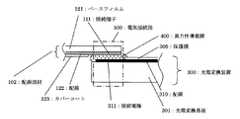
図4は、光電変換装置300と配線部材102の電気接続部の拡大図であり、図4(A)は、図3(A)a部の模式的部分拡大平面図、図4(B)は、図4(A)のA−−−A′の模式的断面図である。 FIG. 4 is an enlarged view of an electrical connection portion between the photoelectric conversion device 300 and the wiring member 102. FIG. 4A is a schematic partial enlarged plan view of FIG. 3A and FIG. FIG. 5 is a schematic cross-sectional view taken along the line A --- A ′ in FIG.
光電変換装置300には、配線部材102との接続をするための接続電極311が基板1上にAl等の導電層により同一ピッチで複数形成されている。305は画素領域に形成された素子の半導体表面や配線を覆い保護安定化するためのSiNx膜等からなる保護層である。 In the photoelectric conversion device 300, a plurality of connection electrodes 311 for connecting to the wiring member 102 are formed on the substrate 1 with a conductive layer such as Al at the same pitch. Reference numeral 305 denotes a protective layer made of a SiNx film or the like for covering and stabilizing the semiconductor surface and wiring of the element formed in the pixel region.
また、配線部材側においては、ポリイミド等からなるベースフィルム121上に形成されたCu等からなる導電層により、接続端子111が接続電極311と同一ピッチで複数形成されている。また、配線部材102には導電層からなる配線130上を覆い保護するエポキシ等からなるカバーコート125が形成されている。 On the wiring member side, a plurality of connection terminals 111 are formed at the same pitch as the connection electrodes 311 by a conductive layer made of Cu or the like formed on a base film 121 made of polyimide or the like. The wiring member 102 is formed with a cover coat 125 made of epoxy or the like that covers and protects the wiring 130 made of a conductive layer.
光電変換装置300に形成された接続電極311と配線部材102に形成された接続端子111とは重なるよう位置決め配置され、異方性導電膜400を用い加熱圧着し電気的に接続されると共に接着固定されている。
しかしながら、光電変換装置の高画質化により画素サイズが小さく高密度化になると外部への接続数が多くなり配線部材102の接続端子111及び光電変換装置の接続電極311を狭ピッチで配置し接続する必要がある。狭ピッチで接続電極を配置した場合、接続ズレのマージンの減少によるショートやオープンなどの接続不良や環境信頼性の低下を引き起こし、製造歩留の悪化による製品のコスト高や製品寿命の低下を招いてしまう。 However, when the pixel size is reduced and the density is increased due to higher image quality of the photoelectric conversion device, the number of connections to the outside increases, and the connection terminals 111 of the wiring member 102 and the connection electrodes 311 of the photoelectric conversion device are arranged and connected at a narrow pitch. There is a need. If the connection electrodes are arranged at a narrow pitch, connection margins such as shorts and opens due to a reduction in connection misalignment and environmental reliability may be reduced, resulting in high product costs and reduced product life due to deteriorated manufacturing yield. I will.
また、画素ピッチ以上で接続電極や接続端子を配置した場合、接続電極の配置の為に光電変換基板が大きくなるという不具合が生じ、更に、配線部材も多く必要となり製造工数の増加による製品のコスト高を招いてしまう。 In addition, when the connection electrodes and connection terminals are arranged at a pixel pitch or more, there is a problem that the photoelectric conversion substrate becomes large due to the arrangement of the connection electrodes, and more wiring members are required, resulting in an increase in manufacturing man-hours. Invite high.
本発明は、以上の点に着目してなされたもので、配線部材の電気接続部を複数列に配置し、各列の電気接続部の構成を同一とすると共に構成する各層の厚さを同一とすることにより、接続電極が増加しても接続電極間のピッチを狭ピッチにせずとも接続電極の配置ができ、更に配線部材と半導体装置との接続が、配線部材の複数列の電気接続部を一括で同時に接続ができ工数があがることなく、且つ安価な装置で安定した接続ができる半導体装置を提供することを目的とする。 The present invention has been made paying attention to the above points, and the electrical connection portions of the wiring members are arranged in a plurality of rows, the configuration of the electrical connection portions in each row is made the same, and the thickness of each layer constituting the same is made the same. As a result, even if the number of connection electrodes increases, the connection electrodes can be arranged without reducing the pitch between the connection electrodes, and the connection between the wiring member and the semiconductor device can be performed in a plurality of rows of electrical connection portions of the wiring member. It is an object of the present invention to provide a semiconductor device that can be connected simultaneously in a lump without increasing man-hours and that can be stably connected with an inexpensive device.
配線部材が、少なくともベースフィルムと2層以上の導電層からなり、接続電極が配置された電気接続部が同一面方向に複数列に配置され、前記複数列の電気接続部の構成が同じであると共に構成する各層の厚さが同じである。 The wiring member is composed of at least a base film and two or more conductive layers, and the electrical connection portions where the connection electrodes are arranged are arranged in a plurality of rows in the same plane direction, and the configuration of the electrical connection portions of the plurality of rows is the same. The thicknesses of the layers constituting the same are the same.
また、前記複数列の電気接続部を構成する各層の材料が同一である。 Moreover, the material of each layer which comprises the said multiple rows | lines electrical connection part is the same.
また、前記複数列の電気接続部における各列の接続電極のパターンが同一で、且つ、電気接続部における各列の接続電極上の導電層が同一パターンで形成されている。 Further, the patterns of the connection electrodes in each column in the plurality of rows of electrical connection portions are the same, and the conductive layers on the connection electrodes in each row in the electrical connection portion are formed in the same pattern.
以上、本発明を整理して要約すれば以下の構成に集約できる。 As described above, if the present invention is organized and summarized, it can be integrated into the following configurations.
(1)二次元的に配列された半導体素子を備える半導体基板と、前記半導体装置を駆動する電気回路基板からなる駆動装置と前記半導体基板を電気的に接続する為の配線部材とを備える半導体装置において、前記配線部材が、少なくともベースフィルムと2層以上の導電層からなり、接続電極が配置された電気接続部が複数列に配置され、前記複数列の電気接続部の構成が同じであると共に構成する各層の厚さが同じであることを特徴とする半導体装置。 (1) A semiconductor device comprising a semiconductor substrate comprising two-dimensionally arranged semiconductor elements, a driving device comprising an electric circuit substrate for driving the semiconductor device, and a wiring member for electrically connecting the semiconductor substrate. The wiring member is composed of at least a base film and two or more conductive layers, the electrical connection portions where the connection electrodes are disposed are disposed in a plurality of rows, and the configuration of the electrical connection portions in the plurality of rows is the same. A semiconductor device characterized in that each layer constituting the same has the same thickness.
(2)前記複数列の電気接続部を構成する各層の材料が同一であることを特徴とする前記(1)記載の半導体装置。 (2) The semiconductor device according to (1), wherein the material of each layer constituting the plurality of rows of electrical connection portions is the same.
(3)前記複数列の電気接続部における各列の接続電極のパターンが同一で、且つ、電気接続部における各列の接続電極上の導電層が同一パターンで形成されていることを特徴とする前記(1)または(2)記載の半導体装置。 (3) The pattern of the connection electrodes in each column in the plurality of rows of electrical connection portions is the same, and the conductive layer on the connection electrode in each row in the electrical connection portion is formed in the same pattern. The semiconductor device according to (1) or (2).
(作用)
よって、配線部材の電気接続部を複数列に配置し、各列の電気接続部の構成を同一とすると共に構成する各層の厚さを同一とすることにより、光電変換装置の高画質化に伴い接続電極が増加しても接続電極間のピッチを狭ピッチにせずとも接続電極の配置が可能となり、更に配線部材と半導体装置との接続が、配線部材の複数列の電気接続部を一括で同時に接続が可能となり工数があがることなく、且つ安価な装置で安定した接続ができる。(Function)
Therefore, by arranging the electrical connection portions of the wiring members in a plurality of rows, making the configuration of the electrical connection portions in each row the same, and making the thickness of each layer the same, with the improvement in the image quality of the photoelectric conversion device Even if the number of connection electrodes increases, it is possible to arrange the connection electrodes without reducing the pitch between the connection electrodes. Furthermore, the connection between the wiring member and the semiconductor device can be performed simultaneously in a plurality of rows of electrical connection portions of the wiring member. Connection is possible and man-hours are not increased, and stable connection can be achieved with an inexpensive device.
更に、配線部材の複数列の電気接続部を構成する各層の材料を同一にし、また、接続端子上の導電層を接続電極と同一パターンで形成することにより、接続時の熱伝導や加圧及び加熱による材料変位を同一にでき、より安定した接続ができる。 Furthermore, by making the material of each layer constituting the plurality of rows of electrical connection portions of the wiring member the same, and forming the conductive layer on the connection terminal in the same pattern as the connection electrode, heat conduction and pressurization at the time of connection and The material displacement by heating can be made the same, and a more stable connection can be made.
以上説明したように、本発明によれば、配線部材の電気接続部を複数列に配置し、各列の電気接続部の構成を同一とすると共に構成する各層の厚さを同一とすることにより、接続電極が増加しても接続電極間のピッチを狭ピッチにせずとも接続電極の配置ができ、更に配線部材と半導体装置との接続が、配線部材の複数列の電気接続部を一括で同時に接続ができ工数があがることなく、且つ安価な装置で安定した接続ができる。 As described above, according to the present invention, the electrical connection portions of the wiring members are arranged in a plurality of rows, and the configuration of the electrical connection portions in each row is the same and the thickness of each layer is the same. Even if the number of connection electrodes increases, the connection electrodes can be arranged without narrowing the pitch between the connection electrodes, and the connection between the wiring member and the semiconductor device can be performed simultaneously in a plurality of rows of electrical connection portions of the wiring member. Connection is possible and man-hours are not increased, and stable connection can be made with an inexpensive device.
よって、高画質、高精細の半導体装置を製造歩留りの低下及び工数の増加なく作製でき、低コストで高品質の半導体装置を提供することができる。 Therefore, a high-quality and high-definition semiconductor device can be manufactured without a decrease in manufacturing yield and an increase in man-hours, and a high-quality semiconductor device can be provided at low cost.
以下、本発明の実施例を図面に基づいて説明する。 Embodiments of the present invention will be described below with reference to the drawings.
図1及び図2は本発明の放射線撮像装置の概略の構成図であり、1図(A)は模式的平面図、図1(B)は図1(A)のA−−−A′の模式的断面図である。 1 and 2 are schematic configuration diagrams of the radiation imaging apparatus of the present invention. FIG. 1 (A) is a schematic plan view, and FIG. 1 (B) is a cross-sectional view taken along line A--A ′ of FIG. 1 (A). It is typical sectional drawing.
尚、前述の従来例の説明に用いた図3(A)、(B)と同一または同等のものには、同一番号を付し、説明を簡略あるいは省略する。 The same or equivalent parts as those shown in FIGS. 3A and 3B used in the description of the above-described conventional example are designated by the same reference numerals, and the description thereof is simplified or omitted.
図1(A)(B)においては配線部材10及び40を用い、配線部材に形成された接続端子と光電変換装置に形成された接続電極が接続されている。 1A and 1B, the wiring members 10 and 40 are used to connect the connection terminals formed on the wiring member and the connection electrodes formed on the photoelectric conversion device.
図2は、光電変換装置3と配線部材10の電気接続部の拡大図であり、図2(A)は、図1(A)のa部の模式的部分拡大平面図、図2(B)(C)及び(D)は、それぞれ図2(A)のA−−−A′の模式的断面図、B−−−B′の模式的断面図、C−−−C′の模式的断面図である。 2 is an enlarged view of an electrical connection portion between the photoelectric conversion device 3 and the wiring member 10, and FIG. 2 (A) is a schematic partial enlarged plan view of a portion in FIG. 1 (A), FIG. 2 (B). (C) and (D) are respectively a schematic cross-sectional view of A --- A ′, a schematic cross-sectional view of B --- B ′, and a schematic cross-section of C --- C ′ in FIG. FIG.
図2(A)及び(B)において、光電変換装置3には、基板1上に配線部材10との接続をするための接続電極がAl等の導電層により第1列の電気接続部50に第1列の接続電極30を、第2列の電気接続部51に第2の接続電極31を同一ピッチでそれぞれの列に複数形成されている。 2A and 2B, in the photoelectric conversion device 3, a connection electrode for connecting to the wiring member 10 on the substrate 1 is connected to the electrical connection portion 50 in the first row by a conductive layer such as Al. A plurality of first connection electrodes 30 are formed in the second row of electrical connection portions 51 and second connection electrodes 31 are formed at the same pitch in each row.
配線部材10は、Cu等からなる第1の導電層14、第2の導電層15、第3の導電層16とポリイミド等の絶縁材料からなる第1のベースフィルム21、第2のベースフィルム22、第3のベースフィルム23とエポキシ等からなるカバーコート25で構成され、接続端子が形成される電気接続部は、光電変換装置3に形成されている接続電極と同様に第1列の電気接続部50に第1列の接続端子11、第2列の電気接続部51に第2列の接続端子12がそれぞれの列に複数形成されている。配線部材10には接続電極以外の第1の導電層14で形成される配線(不図示)上を覆い保護するエポキシ等からなるカバーコート25が形成されている。 The wiring member 10 includes a first conductive layer 14 made of Cu or the like, a second conductive layer 15, a third conductive layer 16, a first base film 21 made of an insulating material such as polyimide, and a second base film 22. The electrical connection portion, which is composed of the third base film 23 and the cover coat 25 made of epoxy or the like, and in which the connection terminals are formed, is electrically connected in the first row in the same manner as the connection electrodes formed in the photoelectric conversion device 3. A plurality of connection terminals 11 in the first row are formed in the section 50, and a plurality of connection terminals 12 in the second row are formed in the second row of electrical connection sections 51. The wiring member 10 is formed with a cover coat 25 made of epoxy or the like that covers and protects the wiring (not shown) formed of the first conductive layer 14 other than the connection electrodes.
光電変換装置3に形成された各列の接続電極と配線部材10に形成された接続端子とは、対向し重なる様配置され、その間に異方性導電膜400を介して電気的に接続されている。異方性導電膜400は、熱硬化性または熱可塑性のフィルム状の接着材内に微小の金属粒子等の導電粒子が分散されており、加熱圧着することにより上・下電極間に存在する導電粒子が圧接触し電気的な接続がなされると共に、接着剤が硬化し、光電変換装置3と配線部材10が接着固定される。 The connection electrodes in each column formed in the photoelectric conversion device 3 and the connection terminals formed in the wiring member 10 are arranged so as to face each other and are electrically connected through the anisotropic conductive film 400 therebetween. Yes. In the anisotropic conductive film 400, conductive particles such as fine metal particles are dispersed in a thermosetting or thermoplastic film adhesive, and the conductive film existing between the upper and lower electrodes by thermocompression bonding. The particles are brought into pressure contact to be electrically connected, the adhesive is cured, and the photoelectric conversion device 3 and the wiring member 10 are bonded and fixed.
図2(B)(C)及び(D)に示すように、第1列及び第2列の電気接続部50、51における配線部材10の構成は同一構成となっており、第1列の電気接続部50は順に、第1列の接続端子11を形成する第1の導電層14、第1のベースフィルム21、第2の導電層15、第2のベースフィルム22で構成され、第2列の電気接続部51は順に、第2列の接続端子12を形成する第2の導電層15、第2のベースフィルム22、第3の導電層16、第3のベースフィルム23で構成されており、電気接続部の構成は、導電層+絶縁層+導電層+絶縁層の構成をなしている。 As shown in FIGS. 2B, 2C, and 2D, the wiring members 10 in the first row and the second row of the electrical connection portions 50 and 51 have the same configuration, and the first row of electric connections The connection part 50 is composed of a first conductive layer 14, a first base film 21, a second conductive layer 15, and a second base film 22 that form the first row of connection terminals 11, in the second row. The electrical connection portion 51 is composed of a second conductive layer 15, a second base film 22, a third conductive layer 16, and a third base film 23 that form the connection terminals 12 in the second row in order. The configuration of the electrical connection portion is a configuration of conductive layer + insulating layer + conductive layer + insulating layer.
更に、第1〜第3の導電層の厚さ及び第1〜第3の絶縁材料からなるベースフィルムの厚さはそれぞれ同一の厚さで構成されおり、本実施例においては、第1〜第3の導電層の厚さを18um、第1〜第3のベースフィルムの厚さを25umで作製した。 Furthermore, the thickness of the first to third conductive layers and the thickness of the base film made of the first to third insulating materials are respectively configured to be the same thickness. The thickness of the conductive layer 3 was 18 μm, and the thickness of the first to third base films was 25 μm.
更に、図2(C)及び(D)に示すように、電気接続部の接続電極上の導電層となる、第1列の電気接続部50の第2の導電層15のパターンと第2列の電気接続部51の第3の導電層16のパターンは同一に形成されており、本実施例においては第1及び第2の接続端子のパターンと同一に形成している。 Further, as shown in FIGS. 2C and 2D, the pattern and the second row of the second conductive layer 15 of the first row of electrical connection portions 50 that become the conductive layer on the connection electrodes of the electrical connection portion. The pattern of the third conductive layer 16 of the electrical connection portion 51 is the same, and in this embodiment, the pattern is the same as the pattern of the first and second connection terminals.
本実施例においては、配線部材10の電気接続部を第1列の電気接続部50と第2列の電気接続部51の2列に配置し接続電極が形成されており、光電変換装置の高画質化に伴い接続電極が増加しても接続電極間のピッチを狭ピッチにせずとも接続電極の配置ができた。また、配線部材10の第1及び第2の電気接続部50、51の構成が同じであると共に構成する各層の厚さが同じであるため、配線部材10の第1及び第2の電気接続部を一括で同時の接続が安価な装置ができた。 In this embodiment, the electrical connection portions of the wiring member 10 are arranged in two rows of the first row electrical connection portion 50 and the second row electrical connection portion 51 to form connection electrodes. Even if the number of connection electrodes increased with the increase in image quality, the connection electrodes could be arranged without reducing the pitch between the connection electrodes. In addition, since the first and second electrical connection portions 50 and 51 of the wiring member 10 have the same configuration and the thicknesses of the layers constituting the same, the first and second electrical connection portions of the wiring member 10 are the same. A device that can be connected simultaneously and at a low cost has been made.
更に、配線部材10の複数列の第1及び第2の電気接続部50、51の構成する各層の材料である第1〜第3の導電層、第1〜第3のベースフィルムが同じであり、また、接続端子上の導電層が接続電極と同一パターンで形成することにより、接続時の熱伝導や加圧及び加熱による材料変位を同一にでき、より安定した接続ができた。 Further, the first to third conductive layers and the first to third base films which are the materials of the respective layers constituting the first and second electric connection portions 50 and 51 of the plurality of rows of the wiring member 10 are the same. In addition, since the conductive layer on the connection terminal is formed in the same pattern as the connection electrode, the heat conduction at the time of connection, the material displacement due to pressurization and heating can be made the same, and a more stable connection can be achieved.
尚、本実施例において配線部材40については説明を省略したが、光電変換装置3との電気接続部を同様に形成し同様の効果を得ることができる。 In addition, although description about the wiring member 40 was abbreviate | omitted in the present Example, the electrical connection part with the photoelectric conversion apparatus 3 can be formed similarly, and the same effect can be acquired.
また、本実施例の半導体装置は、放射線撮像装置を一例に説明したが、半導体基板の光電変換装置を発光素子や液晶制御素子などを備える表示装置にすることによって液晶テレビ等の画像表示装置においてもの同様の効果を得る事ができる。 The semiconductor device of the present embodiment has been described by taking the radiation imaging device as an example. However, in the image display device such as a liquid crystal television by changing the photoelectric conversion device of the semiconductor substrate to a display device including a light emitting element and a liquid crystal control element. The same effect can be obtained.
1 光電変換基板
3,300 光電変換装置(半導体基板)
4 放射線可視光変換装置
10,40,101,102 配線部材
11,12,111,112 接続端子
14,15,16 導電層
21,22,23,121 ベースフィルム
25,125 カバーコート
30,31,311 接続電極
50,51,500 電気接続部
60,70,600,700 半導体からなる電子部品
130 配線(配線部材上の)
305 保護膜
310 配線(光電変換基板上の)
400 異方性導電膜1 Photoelectric conversion substrate 3,300 Photoelectric conversion device (semiconductor substrate)
4 Radiation-visible light conversion device 10, 40, 101, 102 Wiring member 11, 12, 111, 112 Connection terminal 14, 15, 16 Conductive layer 21, 22, 23, 121 Base film 25, 125 Cover coat 30, 31, 311 Connection electrode 50, 51, 500 Electrical connection part 60, 70, 600, 700 Electronic component 130 made of semiconductor Wiring (on wiring member)
305 Protective film 310 Wiring (on photoelectric conversion substrate)
400 Anisotropic conductive film
Claims (3)
Translated fromJapanesePriority Applications (1)
| Application Number | Priority Date | Filing Date | Title |
|---|---|---|---|
| JP2003359106AJP2005123506A (en) | 2003-10-20 | 2003-10-20 | Semiconductor device |
Applications Claiming Priority (1)
| Application Number | Priority Date | Filing Date | Title |
|---|---|---|---|
| JP2003359106AJP2005123506A (en) | 2003-10-20 | 2003-10-20 | Semiconductor device |
Publications (1)
| Publication Number | Publication Date |
|---|---|
| JP2005123506Atrue JP2005123506A (en) | 2005-05-12 |
Family
ID=34615438
Family Applications (1)
| Application Number | Title | Priority Date | Filing Date |
|---|---|---|---|
| JP2003359106AWithdrawnJP2005123506A (en) | 2003-10-20 | 2003-10-20 | Semiconductor device |
Country Status (1)
| Country | Link |
|---|---|
| JP (1) | JP2005123506A (en) |
Cited By (2)
| Publication number | Priority date | Publication date | Assignee | Title |
|---|---|---|---|---|
| JP2007147525A (en)* | 2005-11-30 | 2007-06-14 | Hitachi Ltd | Eddy current flaw detection probe and lift-off amount evaluation method of test object, its evaluation apparatus, eddy current flaw detection method and eddy current flaw detection apparatus |
| WO2017163953A1 (en)* | 2016-03-25 | 2017-09-28 | ソニー株式会社 | Semiconductor device, solid imaging element, imaging device, and electronic apparatus |
- 2003
- 2003-10-20JPJP2003359106Apatent/JP2005123506A/ennot_activeWithdrawn
Cited By (4)
| Publication number | Priority date | Publication date | Assignee | Title |
|---|---|---|---|---|
| JP2007147525A (en)* | 2005-11-30 | 2007-06-14 | Hitachi Ltd | Eddy current flaw detection probe and lift-off amount evaluation method of test object, its evaluation apparatus, eddy current flaw detection method and eddy current flaw detection apparatus |
| WO2017163953A1 (en)* | 2016-03-25 | 2017-09-28 | ソニー株式会社 | Semiconductor device, solid imaging element, imaging device, and electronic apparatus |
| US10680026B2 (en) | 2016-03-25 | 2020-06-09 | Sony Corporation | Semiconductor device, solid-state image pickup element, image pickup device, and electronic apparatus |
| US11923395B2 (en) | 2016-03-25 | 2024-03-05 | Sony Group Corporation | Semiconductor device, solid-state image pickup element, image pickup device, and electronic apparatus |
Similar Documents
| Publication | Publication Date | Title |
|---|---|---|
| US8823872B2 (en) | Image pickup module with improved flatness of image sensor and via electrodes | |
| US10283064B2 (en) | Liquid crystal display, device and connection structure of display panel and system circuit | |
| US9293434B2 (en) | Electronic device mounted on a substrate | |
| US20050104991A1 (en) | Imaging element, imaging device, camera module and camera system | |
| WO2010070735A1 (en) | Optical matrix device | |
| JP2004242166A (en) | Optical module, method of manufacturing the same, and electronic device | |
| WO2020039733A1 (en) | Semiconductor device, electronic apparatus, and method for manufacturing semiconductor device | |
| WO2019007412A1 (en) | Encapsulation structure of image sensing chip, and encapsulation method therefor | |
| US12167114B2 (en) | Image pickup module, image pickup apparatus, and electronic device | |
| US20010027873A1 (en) | Image pickup device and portable telephone | |
| WO2017138443A1 (en) | Semiconductor device and display device | |
| JP2005123506A (en) | Semiconductor device | |
| JP7467168B2 (en) | Image pickup device and imaging device | |
| EP1154638A1 (en) | Image pickup device and portable telephone | |
| JP4693224B2 (en) | TAB tape and radiation imaging apparatus | |
| JP2005123259A (en) | Manufacturing method of semiconductor device | |
| US12418983B2 (en) | Electronic module and apparatus | |
| JP2008166521A (en) | Solid-state imaging device | |
| JP3817859B2 (en) | Imaging device | |
| JP2005100896A (en) | Semiconductor device connection structure and semiconductor device having the connection structure | |
| JP7739730B2 (en) | Imaging unit and imaging device | |
| JP3849248B2 (en) | Imaging device | |
| TWI811751B (en) | Connector assembly and sensor system | |
| US11675094B2 (en) | X-ray device | |
| JP3118805B2 (en) | Mounting structure of sensor and its signal processing circuit |
Legal Events
| Date | Code | Title | Description |
|---|---|---|---|
| A300 | Application deemed to be withdrawn because no request for examination was validly filed | Free format text:JAPANESE INTERMEDIATE CODE: A300 Effective date:20070109 |