JP2005123089A - Color organic EL display and manufacturing method thereof - Google Patents
Color organic EL display and manufacturing method thereofDownload PDFInfo
- Publication number
- JP2005123089A JP2005123089AJP2003358320AJP2003358320AJP2005123089AJP 2005123089 AJP2005123089 AJP 2005123089AJP 2003358320 AJP2003358320 AJP 2003358320AJP 2003358320 AJP2003358320 AJP 2003358320AJP 2005123089 AJP2005123089 AJP 2005123089A
- Authority
- JP
- Japan
- Prior art keywords
- organic
- layer
- color
- color conversion
- conversion filter
- Prior art date
- Legal status (The legal status is an assumption and is not a legal conclusion. Google has not performed a legal analysis and makes no representation as to the accuracy of the status listed.)
- Pending
Links
Images


Landscapes
- Electroluminescent Light Sources (AREA)
Abstract
Translated fromJapaneseDescription
Translated fromJapanese本発明は、長期の信頼性を有するカラー有機ELディスプレイおよびその製造方法に関する。特に本発明は、色変換フィルタ基板と有機EL素子を貼り合わせた形式のカラー有機ELディスプレイにおいて、貼り合わせた際の間隙に所定機能を有する隔壁を設けたものおよび該カラー有機ELディスプレイの製造方法に関する。 The present invention relates to a color organic EL display having long-term reliability and a manufacturing method thereof. In particular, the present invention relates to a color organic EL display of a type in which a color conversion filter substrate and an organic EL element are bonded together, in which a partition having a predetermined function is provided in the gap when bonded, and a method for manufacturing the color organic EL display About.
近年、情報技術の多様化が進んでおり、該分野における素子の中でも、表示デバイスについては、「美・軽・薄・優」が求められ、さらに、低消費電力・高速応答へ向けて活発な開発が進められている。特に、高精細なフルカラー表示デバイスにおける開発が広くなされている。 In recent years, the diversification of information technology has progressed, and among the elements in this field, display devices require “beauty, lightness, thinness, and excellence”, and they are also active toward low power consumption and high-speed response. Development is underway. In particular, development in high-definition full-color display devices has been widely performed.
1980年の後半に、Tangらによって、有機分子薄膜を積層した構造を有する有機エレクトロルミネセンス(以下有機ELという)が印加電圧10Vにおいて1000cd/m2以上の高輝度が得られるとの報告(非特許文献1参照)がなされた。この積層型有機EL素子は、液晶表示素子等に比べて、視野角依存性、高速応答性などの特性に優れており、前記Tangらの報告をきっかけとして、その後、有機EL素子の研究が活発に行われており、一部実用化もされている。また、有機高分子材料を用いた同様の素子も活発に開発が進められている。In the latter half of 1980, Tang et al. Reported that organic electroluminescence having a structure in which organic molecular thin films were laminated (hereinafter referred to as organic EL) can obtain high luminance of 1000 cd / m2 or more at an applied voltage of 10 V (non- (See Patent Document 1). This multilayer organic EL element is superior in characteristics such as viewing angle dependency and high-speed response compared to a liquid crystal display element and the like. Based on the report by Tang et al. Have been put into practical use. Similar devices using organic polymer materials are also being actively developed.
有機EL素子は、低電圧で高い電流密度が実現できるため、無機EL素子やLEDに比べて高い発光輝度と発光効率が期待できる。 Since an organic EL element can realize a high current density at a low voltage, it can be expected to have higher light emission luminance and light emission efficiency than inorganic EL elements and LEDs.
有機ELディスプレイとしての特徴には、高輝度および高コントラストであること、低電圧駆動および高い発光効率であること、高解像度であること、高視野性であること、応答速度が速いこと、微細化およびカラー化が可能であること、軽さと薄さを備えること等がある。以上の点から、有機EL素子の美・軽・薄・優なフラットパネルディスプレイへの応用が期待されている。 Features as an organic EL display include high brightness and high contrast, low voltage drive and high luminous efficiency, high resolution, high field of view, fast response speed, miniaturization In addition, there is a possibility of colorization, provision of lightness and thinness, and the like. From the above points, application of organic EL elements to beautiful, light, thin, and excellent flat panel displays is expected.
また、有機ELディスプレイのマルチカラーまたはフルカラー化も盛んに検討されている。有機ELディスプレイのマルチカラーまたはフルカラー化の方法としては、有機EL素子の発光域の光を吸収し、可視光域の蛍光を発光する蛍光材料をフィルタに用いる色変換方式と呼ばれる方式が、提案されている(特許文献1および2など参照)。この方式では、有機EL素子の発光色は白色に限定されないため、より輝度の高い有機EL素子を光源に適用でき、青色発光の有機EL素子を用いた色変換方式(特許文献3〜5参照)では、青色光を緑色光や赤色光に波長変換している。波長変換作用を有する蛍光色素を含む蛍光変換膜を高精細にパターニングすれば、発光体の近紫外光ないし可視光のような弱いエネルギー線を用いても、フルカラーの発光型ディスプレイが構築できる。このような色変換方式を採用する有機ELディスプレイのうち、蛍光変換膜を含む色変換フィルタ基板と有機EL素子を貼り合わせてフルカラー化を達成するものがある。このようなカラー有機ELディスプレイを作成する場合、色変換フィルタと有機EL素子を貼り合わせる際に色変換フィルタと有機EL素子の間隔を一定に保つための隔壁または支柱を画素間に設けることが行われている(特許文献6参照)。 In addition, multi-color or full-color organic EL displays have been actively studied. As a method for making the organic EL display multi-colored or full-colored, a method called a color conversion method using a fluorescent material that absorbs light in the light emitting region of the organic EL element and emits fluorescence in the visible light region as a filter has been proposed. (See Patent Documents 1 and 2, etc.). In this method, since the emission color of the organic EL element is not limited to white, an organic EL element having higher luminance can be applied to the light source, and a color conversion method using a blue light-emitting organic EL element (see Patent Documents 3 to 5) Then, the wavelength of blue light is converted into green light or red light. If a fluorescent conversion film containing a fluorescent dye having a wavelength converting action is patterned with high definition, a full-color light-emitting display can be constructed even using weak energy rays such as near-ultraviolet light or visible light of a light emitter. Among organic EL displays that employ such a color conversion method, there are some that achieve full color by bonding a color conversion filter substrate including a fluorescent conversion film and an organic EL element. When creating such a color organic EL display, it is necessary to provide a partition or support between the pixels to keep the distance between the color conversion filter and the organic EL element constant when the color conversion filter and the organic EL element are bonded together. (See Patent Document 6).
また、カラー有機ELディスプレイは、素子内を乾燥環境下に置くため、素子内に乾燥剤などを配置することも開示されている(特許文献7〜10など参照)。 In addition, since the color organic EL display is placed in a dry environment, it is also disclosed that a desiccant or the like is placed in the element (see Patent Documents 7 to 10).
上記のような隔壁や支柱には光透過性のレジストなどが用いられるが、光透過性のものでは、隣の画素への光のクロストークが生じ問題であった。また、貼り合わせによりカラー有機ELディスプレイを製造する場合、色変換フィルタと有機EL素子の間の間隙が狭すぎるため、シート状の吸湿剤を挿入することが困難であり、素子内の乾燥が不十分となり、カラー有機ELディスプレイの長期間の信頼性に問題があった。 A light-transmitting resist or the like is used for the above-described partition walls and support columns. However, in the case of the light-transmitting resist, crosstalk of light to an adjacent pixel occurs, which is a problem. In addition, when a color organic EL display is manufactured by bonding, the gap between the color conversion filter and the organic EL element is too narrow, so that it is difficult to insert a sheet-like moisture absorbent, and drying in the element is difficult. There was a problem with the long-term reliability of the color organic EL display.
そこで本発明の目的は、色変換フィルタと有機EL素子間の間隙を隔壁により一定に保ち、該隔壁の光のクロストークを防止し、隔壁による光の吸収を防止したカラー有機ELディスプレイを提供することである。さらに、本発明の目的は、該隔壁に吸湿効果も併せ持たせ、長期安定性を有するカラー有機ELディスプレイを提供することである。 SUMMARY OF THE INVENTION Accordingly, an object of the present invention is to provide a color organic EL display that keeps the gap between the color conversion filter and the organic EL element constant by the partition wall, prevents light crosstalk of the partition wall, and prevents light absorption by the partition wall. That is. Furthermore, an object of the present invention is to provide a color organic EL display having long-term stability by providing the partition wall with a moisture absorption effect.
本発明の第一の側面は、カラー有機ELディスプレイに関する。このカラー有機ELディスプレイは、色変換フィルタ基板と有機EL素子を、間隙を介して貼り合わせたカラー有機ELディスプレイであり、このカラー有機ELディスプレイの前記間隙に光散乱性または反射性の隔壁を形成したことを特徴とする。 The first aspect of the present invention relates to a color organic EL display. This color organic EL display is a color organic EL display in which a color conversion filter substrate and an organic EL element are bonded via a gap, and a light-scattering or reflective partition is formed in the gap of the color organic EL display. It is characterized by that.
本発明の第二の側面は、カラー有機ELディスプレイの製造方法である。この製造方法は、(a)色変換フィルタ基板と有機EL素子を提供する工程と、(b)前記色変換フィルタ基板上または前記有機EL素子上のいずれか一方に光散乱性または光反射性である隔壁を形成する工程と、(c)色変換フィルタ基板に隔壁を形成した場合には、隔壁を形成した色変換フィルタ基板と有機EL素子とを貼り合わせ、有機EL素子に隔壁を形成した場合には、色変換フィルタと隔壁を形成した有機EL素子とを貼り合わせる工程とを含む。本発明の第一の側面および第二の側面では、隔壁が吸湿性を有することを特徴とする。 The second aspect of the present invention is a method for producing a color organic EL display. This manufacturing method includes (a) a step of providing a color conversion filter substrate and an organic EL element, and (b) light scattering or light reflecting on either the color conversion filter substrate or the organic EL element. A step of forming a partition; and (c) when the partition is formed on the color conversion filter substrate, the color conversion filter substrate on which the partition is formed and the organic EL element are bonded, and the partition is formed on the organic EL element Includes a step of bonding the color conversion filter and the organic EL element on which the partition walls are formed. In the first aspect and the second aspect of the present invention, the partition wall is hygroscopic.
本発明のカラー有機ELディスプレイは、光反射性または光散乱性の微粉末を含む材料で構成されるため、色変換フィルタ基板へ斜めに入射する有機EL素子からの光が色変換フィルタ層側へ反射されるので、隣接画素への光のクロストークが防止される。また、微粉末は吸湿性であるのでディスプレイ内の雰囲気を乾燥させることもでき、カラー有機ELディスプレイの信頼性の向上につながる。 Since the color organic EL display of the present invention is made of a material containing a light-reflective or light-scattering fine powder, light from the organic EL element obliquely incident on the color conversion filter substrate is directed to the color conversion filter layer side. Since the light is reflected, crosstalk of light to adjacent pixels is prevented. Further, since the fine powder is hygroscopic, the atmosphere in the display can be dried, leading to an improvement in the reliability of the color organic EL display.
本発明のカラー有機ELディスプレイの製造方法は、クロストークを防止し、長期安定性に優れるカラー有機ELディスプレイを提供できる。 The method for producing a color organic EL display of the present invention can provide a color organic EL display that prevents crosstalk and is excellent in long-term stability.
本発明のカラー有機ELディスプレイおよびその製造方法を具体的に説明する。以下の説明では、適宜図面を参照するが、図面に示される有機EL素子およびその製造方法は、例示であり、本発明はこれに限定されない。 The color organic EL display and the manufacturing method thereof of the present invention will be specifically described. In the following description, the drawings are referred to as appropriate, but the organic EL element and the manufacturing method thereof shown in the drawings are exemplifications, and the present invention is not limited thereto.
まず、本発明のカラー有機ELディスプレイについて図1および図2を参照して説明する。図1は、本発明のカラー有機ELディスプレイの第一の実施形態(アクティブマトリックス型(以下TFT型とも称する))を示す概略断面図である。図2は、本発明のカラー有機ELディスプレイの第二の実施形態(パッシブマトリックス型)を示す概略断面図である。 First, the color organic EL display of the present invention will be described with reference to FIG. 1 and FIG. FIG. 1 is a schematic sectional view showing a first embodiment (active matrix type (hereinafter also referred to as TFT type)) of a color organic EL display of the present invention. FIG. 2 is a schematic sectional view showing a second embodiment (passive matrix type) of the color organic EL display of the present invention.
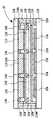
本発明のカラー有機ELディスプレイの第一の実施形態は、図1に示される、いわゆるトップエミッション方式のアクティブマトリックス型カラー有機ELディスプレイ10である。本発明のカラー有機ELディスプレイ10は、色変換フィルタ基板と有機EL素子を貼り合わせた構造を有する。本発明では、色変換フィルタ基板と有機EL素子は所定の間隙を介して張り合わされ、この間隙の部分に隔壁124が設けられる。 The first embodiment of the color organic EL display of the present invention is a so-called top emission type active matrix color
有機EL素子は、支持基板102上にTFT、平坦化層112、さらに下部電極104と、その上に設けられた有機発光層116、上部電極106を有する。本発明では、有機EL素子には、パッシベーション層114aを設けることが好ましい。 The organic EL element includes a TFT, a
色変換フィルタ基板は、透明基板118上にブラックマトリックス108、色変換層110、オーバーコート層128およびパッシベーション層114bを設けたものである。 In the color conversion filter substrate, a
本発明のカラー有機ELディスプレイは、この色変換フィルタ基板および有機EL素子を外周封止層120を用いて貼り合わせ、必要に応じて充填剤層126を設ける。また、本発明のカラー有機ELディスプレイは、色変換フィルタ基板と有機EL素子の間の間隙であって、色変換フィルタ層のない部分、即ちサブピクセル間に隔壁124を有する。 In the color organic EL display of the present invention, the color conversion filter substrate and the organic EL element are bonded together using the outer
図1では、カラー有機ELディスプレイは一画素として表してあるが、複数の画素の場合は、有機EL素子には、対応する複数の薄膜トランジスタとパターンニングした下部電極を設け、色変換フィルタ基板には、このパターンに相当する色変換フィルタ層を設ければよい。 In FIG. 1, the color organic EL display is represented as one pixel. However, in the case of a plurality of pixels, the organic EL element is provided with a plurality of corresponding thin film transistors and a patterned lower electrode, and the color conversion filter substrate is provided on the color conversion filter substrate. A color conversion filter layer corresponding to this pattern may be provided.
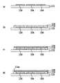
本発明の第二の実施形態は、図2に示される、いわゆるトップエミッション方式のパッシブマトリックス型カラー有機ELディスプレイ20である。図2に示されるように、本発明のカラー有機ELディスプレイは、パッシブマトリックス型の有機EL素子と、色変換フィルタ基板を貼り合わせたものである。 The second embodiment of the present invention is a so-called top emission type passive matrix color
有機EL素子は、支持基板102上に下部電極104と、その上に設けられた有機発光層116、上部電極106を有する。さらに図2では、一画素として本発明のカラー有機ELディスプレイを表したが、複数の画素を含むことでき、この場合、これをパッシブマトリクス方式で駆動するには、下部電極および上部電極はそれぞれラインパターン状に形成され、下部電極のラインパターンと上部電極のラインパターンは直交する方向に延びることができる。 The organic EL element has a
なお、本発明では、下部電極上には任意に絶縁膜(図示せず)を設けることができる。また本発明では、有機EL素子の気密性を保つため、上部電極および有機発光層上にパッシベーション層114aを設けることが好ましい。また、支持基板102上には、任意に反射膜(図示せず)を設けてもよい。 In the present invention, an insulating film (not shown) can be arbitrarily provided on the lower electrode. Moreover, in this invention, in order to maintain the airtightness of an organic EL element, it is preferable to provide the
色変換フィルタ基板は、上記第一の実施形態で説明したものと同じである。 The color conversion filter substrate is the same as that described in the first embodiment.
本発明のカラー有機ELディスプレイでは、この色変換フィルタ基板および有機EL素子を、外周封止層120を用いて貼り合わせ、必要に応じて充填剤層126を設ける。また、本発明のカラー有機ELディスプレイは、色変換フィルタ基板と有機EL素子の間の間隙であって、色変換フィルタ層のない部分、即ちサブピクセル間に隔壁124を有する。図2に示されるように、本発明のカラー有機ELディスプレイは、隔壁124を間隙の部分に設けることを特徴とする。 In the color organic EL display of the present invention, the color conversion filter substrate and the organic EL element are bonded together using the outer
以下に本発明のカラー有機ELディスプレイの隔壁124について説明する。
本発明では隔壁124は、有機EL素子と色変換フィルタ基板の基板間の間隙に設けられ、この間隙を一定の間隔に保つ。また、この隔壁は、光のクロストークを防止し、隔壁による光の吸収を防止する。さらにこの隔壁は、吸湿効果を有する。このような機能を有する本発明の隔壁は、例えばレジスト材料に、上記機能を有する微粉末を混合したものからなる。レジスト材料としては、有機フォトレジスト(例えば商品名ZPN1000(日本ゼオン製)など)などを好適に用いることができる。The
In the present invention, the
また、本発明の隔壁に含有される微粉末は、例えば、光反射性または光散乱性の材料、光反射性または光散乱性の材料であって吸湿性を有する材料、光反射性または光散乱性の材料と吸湿剤の混合物などが挙げられる。具体的には、光反射性または光散乱性の材料としては、例えばAl、Zn、Ti、Agなどの金属微粉末が挙げられる。本発明では、隔壁がパッシベーション層のような絶縁性の膜上に形成される限り、導電性であってもよい。 In addition, the fine powder contained in the partition wall of the present invention is, for example, a light-reflective or light-scattering material, a light-reflective or light-scattering material and a hygroscopic material, light-reflective or light-scattering. For example, a mixture of a water-soluble material and a hygroscopic agent. Specifically, examples of the light reflective or light scattering material include fine metal powders such as Al, Zn, Ti, and Ag. In the present invention, as long as the partition wall is formed on an insulating film such as a passivation layer, it may be conductive.
光反射性または光散乱性の材料であって吸湿性を有する材料としては、例えばTiO2、CaO、SrO、BaOなどの吸湿性のある白色酸化物粉末、光反射性または光散乱性の材料と吸湿剤の混合物としては、例えば上記Al、Zn、Ti、Agと活性シリカ、ゼオライトなどとの混合物が挙げられる。特に本発明では、吸湿性のある白色微粉末が好ましい。Examples of the light-reflective or light-scattering material that has hygroscopicity include, for example, a white oxide powder having hygroscopicity such as TiO2 , CaO, SrO, and BaO, a light-reflective or light-scattering material, and the like. As a mixture of a hygroscopic agent, the mixture of said Al, Zn, Ti, Ag, activated silica, zeolite etc. is mentioned, for example. In the present invention, a white fine powder having hygroscopicity is particularly preferable.
本発明では、レジスト材料と光反射性または光散乱性材料の比率は、1:1〜10:1、好ましくは5:1である。 In the present invention, the ratio of resist material to light reflective or light scattering material is 1: 1 to 10: 1, preferably 5: 1.
本発明の隔壁は、有機EL素子と色変換フィルタ基板の間の間隙に設けられるので、隔壁の厚さは、この間隙の寸法であり、1〜30μmであることが好ましい。 Since the partition wall of the present invention is provided in the gap between the organic EL element and the color conversion filter substrate, the thickness of the partition wall is the dimension of this gap, and is preferably 1 to 30 μm.
このように本発明の隔壁を、上記のような微粉末を含む材料で構成することにより光反射性または光散乱性とする(不透明化する)ことにより、色変換フィルタ基板へ斜めに入射する有機EL素子からの光が、色変換フィルタ層側へ反射されるので、隣接画素への光のクロストークが防止される。また、微粉末が吸湿性である場合にはディスプレイ内の雰囲気を乾燥させることもでき、カラー有機ELディスプレイの信頼性の向上につながる。特に吸湿性のある白色微粉末を含む隔壁(白色の隔壁)を用いることにより、上記特性をすべて併せ持つカラー有機ELディスプレイを構築することができる。 As described above, the partition wall of the present invention is made of a material containing the fine powder as described above to make it light reflective or light scattering (opaque), so that the organic light incident obliquely on the color conversion filter substrate is obtained. Since light from the EL element is reflected to the color conversion filter layer side, crosstalk of light to adjacent pixels is prevented. Further, when the fine powder is hygroscopic, the atmosphere in the display can be dried, leading to an improvement in the reliability of the color organic EL display. In particular, a color organic EL display having all of the above characteristics can be constructed by using partition walls (white partition walls) containing white hygroscopic powder.
以下に本発明の有機EL素子と色変換フィルタ基板の各要素について説明する。なお、以下の説明では、図3または図4に示されていない任意要素についても説明する。 Hereinafter, each element of the organic EL element and the color conversion filter substrate of the present invention will be described. In the following description, optional elements not shown in FIG. 3 or 4 will be described.
(I)有機EL素子
(i)下部電極、有機発光層および上部電極
本発明の有機EL素子は、一対の電極の間に少なくとも有機発光層を挟持し、必要に応じ、正孔注入層や電子注入層などを導入した構造を有する。即ち、本発明の有機EL素子は、下部電極と、正孔注入層、有機発光層、電子輸送層などを含む有機発光層と上部電極とを少なくとも含む。具体的には、例えば、下記のような層構造を有する。
(1)陽極/有機EL層/陰極
(2)陽極/正孔注入層/有機EL層/陰極
(3)陽極/有機発光層/電子輸送層/陰極
(4)陽極/正孔注入層/有機EL層/電子輸送層/陰極
(5)陽極/正孔注入層/正孔輸送層/有機EL層/電子輸送層/陰極
(6)陽極/正孔注入層/正孔輸送層/有機EL層/電子輸送層/電子注入層/陰極(I) Organic EL device (i) Lower electrode, organic light emitting layer and upper electrode The organic EL device of the present invention sandwiches at least an organic light emitting layer between a pair of electrodes, and if necessary, a hole injection layer or an electron. It has a structure in which an injection layer or the like is introduced. That is, the organic EL device of the present invention includes at least a lower electrode, an organic light emitting layer including a hole injection layer, an organic light emitting layer, an electron transport layer, and the like, and an upper electrode. Specifically, for example, it has the following layer structure.
(1) Anode / organic EL layer / cathode (2) Anode / hole injection layer / organic EL layer / cathode (3) Anode / organic light emitting layer / electron transport layer / cathode (4) Anode / hole injection layer / organic EL layer / electron transport layer / cathode (5) anode / hole injection layer / hole transport layer / organic EL layer / electron transport layer / cathode (6) anode / hole injection layer / hole transport layer / organic EL layer / Electron transport layer / electron injection layer / cathode
上記の層構造において、陽極および陰極の少なくとも一方(本発明では上部電極)は、有機発光層の発する光の波長域において透明である。この透明な電極を通して光が放出される。 In the above layer structure, at least one of the anode and the cathode (in the present invention, the upper electrode) is transparent in the wavelength range of light emitted by the organic light emitting layer. Light is emitted through this transparent electrode.
なお、本明細書において、下部電極および上部電極に挟持された有機層(有機EL層、正孔注入層、正孔輸送層、電子輸送層および/または電子注入層)の部分を有機発光層と称する。また、本明細書において、下部電極、有機発光層、および上部電極を併せて発光部と称する。 In this specification, a portion of an organic layer (organic EL layer, hole injection layer, hole transport layer, electron transport layer and / or electron injection layer) sandwiched between the lower electrode and the upper electrode is referred to as an organic light emitting layer. Called. Moreover, in this specification, a lower electrode, an organic light emitting layer, and an upper electrode are collectively called a light emission part.
まず、下部電極および上部電極について説明する。本発明では、以下に示す下部電極および上部電極を用いることができる。 First, the lower electrode and the upper electrode will be described. In the present invention, the following lower electrode and upper electrode can be used.
イ)下部電極(104)
下部電極104は、TFT型の場合、支持基板上にパターンニングされたTFTが形成され、その上の平坦化層が形成され、この平坦化層上に下部電極が形成される。各画素に対応した下部電極104とTFTはソース電極またはドレイン電極により接続される。パッシブマトリックス型の場合、支持基板102上に形成される。下部電極104は、有機発光層に対して効率よく電子または正孔を注入することができるものである。下部電極は、陽極または陰極として用いることができるが、本発明では陽極として用いることが好ましい。B) Lower electrode (104)
When the
下部電極を陽極として用いる場合、正孔の注入を効率よく行うために、仕事関数が大きい材料が用いられる。トップエミッション方式である本発明の有機EL素子では下部電極は透明であることは必要ではないが、ITO、IZOなどの導電性金属酸化物を用いて下部電極を形成することができる。さらに、ITOなどの導電性金属酸化物を用いる場合、その下に反射率の高いメタル電極(Al,Ag,Mo,Wなど)を用いることが好ましい。このメタル電極は、導電性金属酸化物より抵抗率が低いので補助電極として機能すると同時に、有機発光層にて発光される光を色変換フィルタ基板側に反射して光の有効利用を図ることが可能となる。また、下部電極は反射機能を持った下部電極とすることができる。具体的には、IZOなどの代わりに反射率の高いNiやCrを紫外線処理して、仕事関数をIZOなどと同等にする。このようにすることにより正孔の注入ができ、所定の反射性金属を陽極として用いることができる。 When the lower electrode is used as an anode, a material having a high work function is used in order to efficiently inject holes. In the organic EL device of the present invention which is a top emission method, the lower electrode does not need to be transparent, but the lower electrode can be formed using a conductive metal oxide such as ITO or IZO. Further, when a conductive metal oxide such as ITO is used, it is preferable to use a metal electrode (Al, Ag, Mo, W, etc.) having a high reflectance underneath. Since this metal electrode has a lower resistivity than the conductive metal oxide, it functions as an auxiliary electrode, and at the same time, the light emitted from the organic light emitting layer can be reflected to the color conversion filter substrate side to effectively use the light. It becomes possible. The lower electrode can be a lower electrode having a reflection function. Specifically, Ni or Cr having a high reflectivity is treated with ultraviolet rays instead of IZO or the like to make the work function equivalent to that of IZO or the like. In this way, holes can be injected and a predetermined reflective metal can be used as the anode.
下部電極を陰極として用いる場合、トップエミッション方式では、仕事関数が小さい材料であるリチウム、ナトリウム等のアルカリ金属、カリウム、カルシウム、マグネシウム、ストロンチウムなどのアルカリ土類金属、またはこれらのフッ化物等からなる電子注入性の金属、その他の金属との合金や化合物が用いられる。前述と同様に、その下に反射率の高いメタル電極(Al,Ag,Mo,Wなど)を用いてもよく、その場合には低抵抗化および反射による有機発光層の発光の有効利用を図ることができる。 When the lower electrode is used as a cathode, the top emission method is made of an alkaline metal such as lithium or sodium, an alkaline earth metal such as potassium, calcium, magnesium or strontium, or a fluoride thereof, which is a material having a low work function. An electron injecting metal or an alloy or compound with other metals is used. Similarly to the above, a metal electrode (Al, Ag, Mo, W, etc.) having a high reflectance may be used underneath, and in that case, low resistance and effective use of light emission of the organic light emitting layer by reflection are achieved. be able to.
ロ)上部電極(108)
上部電極は、有機発光層に対して効率よく電子または正孔を注入することができるものである。B) Upper electrode (108)
The upper electrode can efficiently inject electrons or holes into the organic light emitting layer.
トップエミッション方式である本発明の場合、上部電極は有機発光層の発光波長域において透明であることが求められる。例えば、上部電極は、波長400〜800nmの光に対して50%以上、好ましくは90%以上の透過率を有することが好ましい。 In the case of the present invention which is a top emission method, the upper electrode is required to be transparent in the light emission wavelength region of the organic light emitting layer. For example, the upper electrode preferably has a transmittance of 50% or more, preferably 90% or more with respect to light having a wavelength of 400 to 800 nm.
トップエミッション方式において上部電極を陰極として用いる場合、有機発光層の発する光の波長域において透明であることが必要とされる。したがって、この場合にはITOまたはIZOのような透明導電性材料を用いることが好ましい。また、上部電極の材料には、電子を効率よく注入するために仕事関数が小さいことが求められる。上記の仕事関数の小さいことと透明であることの2つの特性を両立するために、本発明において上部電極は透明電極層と仕事関数の小さい材料からなる層(これは、有機発光層中の電子注入層に相当する。)との複数層からなっていてもよい。一般に、仕事関数の小さい材料は、透明性が低いので、このようにすることは有効である。例えば、リチウム、ナトリウム等のアルカリ金属、カリウム、カルシウム、マグネシウム、ストロンチウムなどのアルカリ土類金属、またはこれらのフッ化物等からなる電子注入性の金属、その他の金属との合金や化合物などの材料の極薄膜(10nm以下)を用いることができる。また、Al、Mg/Agのような材料を用いることもできる。 When the top electrode is used as a cathode in the top emission method, it is required to be transparent in the wavelength range of light emitted from the organic light emitting layer. Therefore, in this case, it is preferable to use a transparent conductive material such as ITO or IZO. The material of the upper electrode is required to have a small work function in order to inject electrons efficiently. In order to satisfy both of the above-mentioned two characteristics of low work function and transparency, in the present invention, the upper electrode is composed of a transparent electrode layer and a layer made of a material having a low work function (this is the electron in the organic light emitting layer). It corresponds to an injection layer). In general, since a material having a small work function has low transparency, this is effective. For example, materials such as alkali metals such as lithium and sodium, alkaline earth metals such as potassium, calcium, magnesium and strontium, or electron injecting metals such as fluorides thereof, alloys and compounds with other metals, etc. An extremely thin film (10 nm or less) can be used. A material such as Al or Mg / Ag can also be used.
これらの仕事関数の小さい材料を用いることにより効率のよい電子注入を可能とし、さらに極薄膜とすることによりこれら材料による透明性低下を最低限とすることが可能となる。この極薄膜の上には、ITOまたはIZOなどの透明導電膜を形成する。上記の極薄膜は補助電極として機能し、上部電極全体の抵抗値を減少させ有機発光層に対して充分な電流を供給することを可能にする。 By using these materials having a low work function, efficient electron injection can be performed, and by using an ultrathin film, it is possible to minimize the decrease in transparency due to these materials. A transparent conductive film such as ITO or IZO is formed on the ultrathin film. The ultrathin film functions as an auxiliary electrode, and reduces the resistance value of the entire upper electrode, making it possible to supply a sufficient current to the organic light emitting layer.
上部電極を陽極として用いる場合、正孔注入効率を高めるために仕事関数の大きな材料を用いる必要がある。トップエミッション方式である場合、有機発光層からの発光が上部電極を通過するために透明性の高い材料を用いる必要がある。したがって、この場合にはITOまたはIZOのような透明導電性材料を用いることが好ましい。 When the upper electrode is used as the anode, it is necessary to use a material having a large work function in order to increase the hole injection efficiency. In the case of the top emission method, it is necessary to use a highly transparent material in order for light emitted from the organic light emitting layer to pass through the upper electrode. Therefore, in this case, it is preferable to use a transparent conductive material such as ITO or IZO.
ハ)有機発光層(116)
有機発光層の各層の材料は、公知のものが使用できる。青色から青緑色の発光を得るためには、有機発光層中に、例えばベンゾチアゾール系、ベンゾイミダゾール系、ベンゾオキサゾール系などの蛍光増白剤、金属キレート化オキソニウム化合物、スチリルベンゼン系化合物、芳香族ジメチリディン系化合物などが好ましく使用される。電子注入層としては、上記電極の欄で説明した仕事関数の小さな材料を使用し、上記極薄膜を電子注入層として機能させることができる。また、電子輸送層としては、金属錯体系(Alq3)とオキサジアゾール、トリアゾール系化合物等を用いることができる。また、正孔注入層としては、芳香族アミン化合物、スターバースト型アミンや、ベンジジン型アミンの多量体および銅フタロシアニン(CuPc)などを用いることができる。正孔輸送層としては、スターバースト型アミン、芳香族ジアミンなどを用いることができる。
上記下部電極および有機発光層の各層の厚さは、従来通りである。C) Organic light emitting layer (116)
As the material of each layer of the organic light emitting layer, known materials can be used. In order to obtain light emission from blue to blue-green, in the organic light emitting layer, for example, optical brighteners such as benzothiazole, benzimidazole and benzoxazole, metal chelated oxonium compounds, styrylbenzene compounds, aromatics Dimethylidin compounds and the like are preferably used. As the electron injection layer, the material having a small work function described in the column of the electrode can be used, and the ultrathin film can function as the electron injection layer. As the electron transport layer, a metal complex (Alq3), oxadiazole, a triazole compound, or the like can be used. For the hole injection layer, aromatic amine compounds, starburst amines, benzidine amine multimers, copper phthalocyanine (CuPc), and the like can be used. As the hole transport layer, a starburst amine, an aromatic diamine, or the like can be used.
The thicknesses of the lower electrode and the organic light emitting layer are the same as conventional ones.
(ii)TFT(122)
TFTは、アクティブマトリクス駆動を行う場合に設けられる。TFTは、支持基板102上にマトリックス状に配置され、各画素に対応した下部電極104にソース電極またはドレイン電極が接続される。好ましくは、TFTは、ゲート電極をゲート絶縁膜の下に設けたボトムゲートタイプで、能動層として多結晶シリコン膜を用いた構造である。(Ii) TFT (122)
The TFT is provided when active matrix driving is performed. The TFTs are arranged in a matrix on the
TFTのドレイン電極およびゲート電極に対する配線部、並びにTFT自身の構造は、所望される耐圧性、オフ電流特性、オン電流特性を達成するように、当該技術において知られている方法により作成することができる。また、トップエミッション方式を用いる本発明の有機ELディスプレイにおいてはTFT部を光が通過しないので、開口率を増加させるためにTFTを小さくする必要がなく、TFT設計の自由度を高くすることができるので、上記の特性を達成するために有利である。 The wiring portion for the drain electrode and the gate electrode of the TFT, and the structure of the TFT itself can be created by a method known in the art so as to achieve the desired withstand voltage, off-current characteristics, and on-current characteristics. it can. In addition, in the organic EL display of the present invention using the top emission method, since light does not pass through the TFT portion, it is not necessary to reduce the TFT in order to increase the aperture ratio, and the degree of freedom in designing the TFT can be increased. Therefore, it is advantageous to achieve the above characteristics.
(iii)平坦化層(112)
アクティブマトリクス駆動を行う場合、平坦化層を、TFT122の上部に形成することが好ましい。平坦化層は、TFT122のソース電極またはドレイン電極と下部電極104との接続およびその他の回路の接続に必要な部分以外に設けられ、基板表面を平坦化して引き続く層の高精細なパターン形成を容易にする。平坦化層は、当該技術に知られている任意の材料により形成することができる。好ましくは、無機酸化物または窒化物、あるいはポリイミドまたはアクリル樹脂から形成される。(Iii) Planarization layer (112)
In the case of performing active matrix driving, a planarization layer is preferably formed on the
(iv)パッシベーション層(114a)
本発明のカラー有機ELディスプレイでは、上部電極以下の各層を覆うパッシベーション層114aを設けることが好ましい。パッシベーション層は、外部環境からの酸素、低分子成分および水分の透過を防止し、それらによる有機発光層の機能低下を防止することに有効である。パッシベーション層は、任意選択の層であるが、上記目的のために設けることが好ましい。パッシベーション層は、有機発光層の発光を外部へと透過させるために、その発光波長域において透明であることが好ましい。(Iv) Passivation layer (114a)
In the color organic EL display of the present invention, it is preferable to provide a
これらの要請を満たすために、パッシベーション層は、可視域における透明性が高く(400〜800nmの範囲で透過率50%以上)、電気絶縁性を有し、水分、酸素および低分子成分に対するバリア性を有し、好ましくは鉛筆硬度2H以上の膜硬度を有する材料で形成される。例えば、SiOx、SiNx、SiNxOy、AlOx、TiOx、TaOx、ZnOx等の無機酸化物、無機窒化物等の材料を使用できる。In order to satisfy these requirements, the passivation layer has high transparency in the visible region (transmittance of 50% or more in the range of 400 to 800 nm), electrical insulation, and barrier property against moisture, oxygen and low molecular components. Preferably, it is formed with the material which has the film hardness of 2H or more of pencil hardness. For example, materials such as inorganic oxides and inorganic nitrides such as SiOx , SiNx , SiNx Oy , AlOx , TiOx , TaOx , and ZnOx can be used.
また、パッシベーション層として種々のポリマー材料を用いることができる。イミド変性シリコーン樹脂(特許文献11〜13)等、無機金属化合物(TiO、Al2O3、SiO2等)をアクリル、ポリイミド、シリコーン樹脂等の中に分散した材料(特許文献14、15)等、アクリレートモノマー/オリゴマー/ポリマーの反応性ビニル基を有した樹脂、レジスト樹脂(特許文献16〜19)等、フッ素系樹脂(特許文献20、21)等、または高い熱伝導率を有するメソゲン構造を有するエポキシ樹脂などの光硬化性樹脂および/または熱硬化性樹脂を挙げることができる。In addition, various polymer materials can be used for the passivation layer. Imide-modified silicone resins (Patent Documents 11 to 13), etc., materials in which inorganic metal compounds (TiO, Al2 O3 , SiO2, etc.) are dispersed in acrylic, polyimide, silicone resins, etc. (Patent Documents 14 and 15), etc. A resin having a reactive vinyl group of acrylate monomer / oligomer / polymer, a resist resin (Patent Documents 16 to 19), a fluorine-based resin (
上述のパッシベーション層は、単層であっても、複数の層が積層されたものであってもよい。パッシベーション層の厚さ(複数の層の積層物である場合は全厚)は、0.1〜10μmであることが好ましい。 The above-described passivation layer may be a single layer or a stack of a plurality of layers. The thickness of the passivation layer (the total thickness in the case of a laminate of a plurality of layers) is preferably 0.1 to 10 μm.
本発明では、後述する色変換フィルタ基板にもパッシベーション層114bを設けることが好ましい。 In the present invention, it is preferable to provide a
(v)支持基板(102)
支持基板102として、ガラスやプラスチックなどからなる絶縁性基板、または、半導電性や導電性基板に絶縁性の薄膜を形成した基板を用いることができる。あるいはまた、ポリオレフィン、アクリル樹脂、ポリエステル樹脂またはポリイミド樹脂などから形成される可撓性フィルムを、支持基板102として用いてもよい。(V) Support substrate (102)
As the supporting
支持基板の膜厚などのパラメータは従来の通りであり、当業者により適切に選択されうる。 Parameters such as the thickness of the support substrate are conventional and can be appropriately selected by those skilled in the art.
本発明では、支持基板102は、少なくとも基板と以下に説明する反射膜から構成されていてもよい。この基板として上記の材料をそのまま使用できる。 In the present invention, the
(vi)反射膜
本発明では、発光部から発せられた光のうち、下部電極側に向かう光を、反射膜を設けることにより上部電極側に効率よく反射させる。本発明で使用されうる反射膜は、特に限定されるものではなく、有機発光層からの光を上部電極側に効率よく反射させることが可能であればよい。例えば光を反射する金属または合金からなるものが挙げられる。透明基板上に設けられる反射膜は、有機発光層の下地層にもなるため平坦性に優れたアモルファス膜とすることが好ましい。アモルファス膜を形成するのに好適な金属および合金としては、CrB、CrP、またはNiPなどが挙げられる。(Vi) Reflective film In the present invention, of the light emitted from the light emitting portion, the light directed to the lower electrode side is efficiently reflected to the upper electrode side by providing the reflective film. The reflective film that can be used in the present invention is not particularly limited as long as it can efficiently reflect light from the organic light emitting layer to the upper electrode side. For example, those made of a metal or an alloy that reflects light can be mentioned. The reflective film provided on the transparent substrate is preferably an amorphous film having excellent flatness because it also serves as a base layer of the organic light emitting layer. Suitable metals and alloys for forming the amorphous film include CrB, CrP, or NiP.
反射膜は、ガラスまたはプラスチックなどの支持基板の上面または裏面(背面)に設けることができる。また、下部電極の形状に合わせてパターン化された反射膜を支持基板上に設けてもよい。 The reflective film can be provided on the upper surface or the back surface (back surface) of a support substrate such as glass or plastic. In addition, a reflective film patterned in accordance with the shape of the lower electrode may be provided on the support substrate.
さらに、支持基板の代りに絶縁層を介して、光を反射する金属または合金からなる基板を用いることにより、基板と反射膜とを兼ねてもよい。反射膜の膜厚などのパラメータは従来の通りであり、当業者により適切に選択されうる。なお、導電性金属を反射膜として用いる場合には、反射膜上に絶縁性の薄膜を形成する。絶縁性の薄膜の材料には、上述のパッシベーション層や平坦化層の無機酸化物膜、無機窒化物膜、有機材料などを用いることができる。 Furthermore, instead of the support substrate, a substrate made of a metal or alloy that reflects light may be used via an insulating layer, so that the substrate and the reflection film may be used together. Parameters such as the thickness of the reflective film are conventional and can be appropriately selected by those skilled in the art. Note that when a conductive metal is used as the reflective film, an insulating thin film is formed on the reflective film. As the material of the insulating thin film, the above-described passivation layer and planarization layer inorganic oxide film, inorganic nitride film, organic material, and the like can be used.
(vii)絶縁膜
本発明の有機EL素子では、支持基板上の下部電極の設けられていない部分に絶縁膜(図示せず)を配設することができる。絶縁膜の材料としては、発光部の駆動電圧に対し、十分な絶縁耐性を有し、且つ、発光部へ悪影響を及ぼさないものであればよい。例えば、無機酸化物膜または無機窒化物膜を用いることが好ましい。このような無機酸化物膜または無機窒化物膜には、例えば、窒化ケイ素、酸化チタン、酸化タンタル、窒化アルミニウム等がある。(Vii) Insulating film In the organic EL device of the present invention, an insulating film (not shown) can be provided on a portion of the support substrate where the lower electrode is not provided. As a material for the insulating film, any material may be used as long as it has sufficient insulation resistance against the driving voltage of the light emitting portion and does not adversely affect the light emitting portion. For example, it is preferable to use an inorganic oxide film or an inorganic nitride film. Examples of such an inorganic oxide film or inorganic nitride film include silicon nitride, titanium oxide, tantalum oxide, and aluminum nitride.
絶縁膜の膜厚などのパラメータは従来の通りであり、当業者により適切に選択されうる。例えば、膜厚は、200〜400nm、好ましくは250〜350nmである。 Parameters such as the thickness of the insulating film are conventional and can be appropriately selected by those skilled in the art. For example, the film thickness is 200 to 400 nm, preferably 250 to 350 nm.
(II)色変換フィルタ基板
色変換フィルタ基板は、上述のように透明基板118に、色変換フィルタ層110(例えば、青色フィルタ層、緑色フィルタと緑色蛍光変換層からなる緑色変換フィルタ層、赤色フィルタ層と赤色蛍光変換層からなる赤色変換フィルタ層)、ブラックマトリックス108、オーバーコート層128、パッシベーション層114bなどを含むことができる。なお、パッシベーション層には、先に(iv)パッシベーション層114aの欄で説明した材料を用いることができる。また、色変換フィルタ基板は、その色変換フィルタ層側を図1および図2に示したように、有機EL素子の上部電極側に対向するように貼り合わせる。貼り合わせに際し、後述する外周封止層120を充填剤層126などを隔壁124と共に用いることができる。(II) Color Conversion Filter Substrate As described above, the color conversion filter substrate is formed on the
以下に本発明の色変換フィルタ基板の各要素について説明する。
1.色変換フィルタ層
本明細書において、色変換フィルタ層は、カラーフィルタ層、蛍光変換層、およびカラーフィルタ層と蛍光変換層との積層体の総称である。蛍光変換層は、有機発光層で発光される近紫外領域ないし可視領域の光、特に青色ないし青緑色領域の光を吸収して異なる波長の可視光を蛍光として発光するものである。フルカラー表示を可能にするためには、少なくとも青色(B)領域、緑色(G)領域および赤色(R)領域の光を放出する独立した色変換フィルタ層が設けられる。RGBそれぞれの蛍光変換層は、少なくとも有機蛍光色素とマトリクス樹脂とを含む。Each element of the color conversion filter substrate of the present invention will be described below.
1. Color Conversion Filter Layer In this specification, the color conversion filter layer is a general term for a color filter layer, a fluorescence conversion layer, and a laminate of a color filter layer and a fluorescence conversion layer. The fluorescence conversion layer absorbs near-ultraviolet to visible light, particularly blue to blue-green light emitted from the organic light-emitting layer, and emits visible light having different wavelengths as fluorescence. In order to enable full color display, an independent color conversion filter layer that emits light of at least the blue (B) region, the green (G) region, and the red (R) region is provided. Each of the RGB fluorescence conversion layers includes at least an organic fluorescent dye and a matrix resin.
本発明では、有機蛍光色素として、少なくとも赤色領域の蛍光を発する蛍光色素の一種類以上が用いられ、緑色領域の蛍光を発する蛍光色素の一種以上と組み合わせることが好ましい。これは以下の理由による。有機発光層が発光源である場合、青色ないし青緑色領域の光を発光するものが得やすいが、これを単なる赤色フィルタに通して赤色領域の光に変更しようとすると、元々赤色領域の波長の光が少ないため、極めて暗い出力光になってしまう。従って、十分な強度の出力を持った赤色領域の光を得るためには、発光体としての有機発光層からの光を蛍光色素によって一旦吸収させ、赤色領域の光に変換させることが必要となる。このように、赤色領域の光は、発光体からの光を蛍光色素によって赤色領域の光に変換させることにより、十分な強度の出力が可能となる。 In the present invention, at least one kind of fluorescent dye that emits fluorescence in the red region is used as the organic fluorescent dye, and it is preferable to combine with one or more fluorescent dyes that emit fluorescence in the green region. This is due to the following reason. When the organic light emitting layer is a light source, it is easy to obtain one that emits light in the blue to blue-green region. However, if this is changed to light in the red region through a simple red filter, the wavelength of the red region is originally increased. Because there is little light, it becomes very dark output light. Therefore, in order to obtain light in the red region having a sufficiently strong output, it is necessary to temporarily absorb the light from the organic light emitting layer as the light emitter by the fluorescent dye and convert it into light in the red region. . As described above, the light in the red region can be output with sufficient intensity by converting the light from the light emitter into the light in the red region by the fluorescent dye.
一方、緑色領域の光は、赤色領域の光と同様に、発光体からの光を別の蛍光色素によって緑色領域の光に変換させて出力させてもよいし、または、発光体の発光が緑色領域の光を十分に含むならば、この発光体からの光を単に緑色フィルタを通して出力してもよい。 On the other hand, the light in the green region may be output by converting the light from the illuminant into the light in the green region by another fluorescent dye, or the light emitted from the illuminant is green. The light from this illuminator may simply be output through the green filter if it contains enough light in the area.
また、青色領域の光に関しては、発光源からの光(例えば有機発光層からの光)を単なる青色フィルタに通して出力させることが可能である。 As for the light in the blue region, light from the light source (for example, light from the organic light emitting layer) can be output through a simple blue filter.
1)有機蛍光色素
本発明において、有機蛍光色素は、有機発光層のような発光体から発せられる近紫外領域ないし可視領域の光、特には青色ないし青緑色領域の光を吸収して、該発光体とは異なる波長の可視光を発するものであれば特に限定されない。1) Organic fluorescent dye In the present invention, the organic fluorescent dye absorbs light in the near-ultraviolet region or visible region, particularly blue or blue-green region, emitted from a light emitter such as an organic light emitting layer, and emits the light. There is no particular limitation as long as it emits visible light having a wavelength different from that of the body.
有機発光層から発せられる青色から青緑色領域の光を吸収して、赤色領域の蛍光を発する蛍光色素には、例えば以下のような有機蛍光色素がある。すなわち、ローダミンB、ローダミン6G、ローダミン3B、ローダミン101、ローダミン110、スルホローダミン、べーシックバイオレット11、べーシックレッド2などのローダミン系色素、シアニン系色素、1−エチル−2−[4−(p−ジメチルアミノフェニル)−13−ブタジエニル]−ピリジウム−パークロレート(ピリジン1)などのピリジン系色素、あるいはオキサジン系色素などである。さらに、各種染料(直接染料、酸性染料、塩基性染料、分散染料など)も所望の蛍光を発することができれば使用することができる。 Examples of fluorescent dyes that absorb blue to blue-green light emitted from the organic light emitting layer and emit red fluorescent light include the following organic fluorescent dyes. That is, rhodamine dyes such as rhodamine B, rhodamine 6G, rhodamine 3B, rhodamine 101,
有機発光層から発せられる青色ないし青緑色領域の光を吸収して、緑色領域の蛍光を発する蛍光色素には、例えば以下のような有機蛍光色素がある。すなわち、3−(2−ベンゾチアゾリル)−7−ジエチルアミノクマリン(クマリン6)、3−(2’−ベンゾイミダゾリル)−7−N,N−ジエチルアミノクマリン(クマリン7)、3−(2’−N−メチルベンゾイミダゾリル)−7−N,N−ジエチルアミノクマリン(クマリン30)、2,3,5,6−1H,4H−テトラヒドロ−8−トリフルオロメチルキノリジン(9,9a,1−gh)クマリン(クマリン153)などのクマリン系色素、または、クマリン色素系染料であるべーシックイエロー51、さらにはソルベントイエロー11、ソルベントイエロー116などのナフタルイミド系色素などである。さらに、各種染料(直接染料、酸性染料、塩基性染料、分散染料など)も所望の蛍光を発することができれば使用することができる。 Examples of fluorescent dyes that absorb blue to blue-green light emitted from the organic light emitting layer and emit green light include the following organic fluorescent dyes. That is, 3- (2-benzothiazolyl) -7-diethylaminocoumarin (coumarin 6), 3- (2′-benzoimidazolyl) -7-N, N-diethylaminocoumarin (coumarin 7), 3- (2′-N-methyl) Benzimidazolyl) -7-N, N-diethylaminocoumarin (coumarin 30), 2,3,5,6-1H, 4H-tetrahydro-8-trifluoromethylquinolidine (9,9a, 1-gh) coumarin (coumarin 153 Or the like, or basic yellow 51 which is a coumarin dye-based dye, and naphthalimide dyes such as solvent yellow 11 and solvent yellow 116. Furthermore, various dyes (direct dyes, acid dyes, basic dyes, disperse dyes, etc.) can be used as long as they can emit desired fluorescence.
なお、本発明に用いることができる有機蛍光色素を、ポリメタクリル酸エステル、ポリ塩化ビニル、塩化ビニル−酢酸ビニル共重合樹脂、アルキッド樹脂、芳香族スルホンアミド樹脂、尿素樹脂、メラミン樹脂、ベンゾグアナミン樹脂およびこれらの樹脂混合物などに予め練り込んで顔料化して、有機蛍光顔料としてもよい。また、これらの有機蛍光色素や有機蛍光顔料(本明細書中で、前記2つを合わせて有機蛍光色素と総称する)は単独で用いてもよく、蛍光の色相を調整するために二種以上を組み合わせて用いてもよい。本発明に用いる有機蛍光色素は、色変換フィルタ層に対して、この変換フィルタ層の重量を基準として0.01〜5重量%、より好ましくは0.1〜2重量%の量で含有される。有機蛍光色素の含有量が0.01重量%未満の場合には、十分な波長変換を行うことができず、その含有量が5%を越える場合には、濃度消光等の効果により色変換効率の低下が起こる。 The organic fluorescent dye that can be used in the present invention includes polymethacrylate, polyvinyl chloride, vinyl chloride-vinyl acetate copolymer resin, alkyd resin, aromatic sulfonamide resin, urea resin, melamine resin, benzoguanamine resin, and An organic fluorescent pigment may be obtained by kneading into a resin mixture or the like in advance to obtain a pigment. In addition, these organic fluorescent dyes and organic fluorescent pigments (in the present specification, the above two are collectively referred to as organic fluorescent dyes) may be used alone, or two or more of them may be used to adjust the hue of fluorescence. May be used in combination. The organic fluorescent dye used in the present invention is contained in an amount of 0.01 to 5% by weight, more preferably 0.1 to 2% by weight, based on the weight of the conversion filter layer, with respect to the color conversion filter layer. . When the content of the organic fluorescent dye is less than 0.01% by weight, sufficient wavelength conversion cannot be performed, and when the content exceeds 5%, color conversion efficiency is obtained due to effects such as concentration quenching. Decrease occurs.
本発明では、色変換フィルタ層の線幅、ピッチなどは、特に制限されない。有機EL素子の目的に合わせて適宜選択すればよい。また、色変換層の膜厚も適宜選択することができるが、例えば10μmとすることができる。 In the present invention, the line width and pitch of the color conversion filter layer are not particularly limited. What is necessary is just to select suitably according to the objective of an organic EL element. The thickness of the color conversion layer can also be selected as appropriate, and can be, for example, 10 μm.
2)マトリックス樹脂
次に、本発明の色変換フィルタ層に用いられるマトリックス樹脂について説明する。マトリックス樹脂は、光硬化性樹脂または光熱併用型の硬化性樹脂からなる。これを、光および/または熱処理して、ラジカル種やイオン種を発生させて重合または架橋させ、樹脂を不溶不融化させて、色変換フィルタ層を形成する。2) Matrix resin Next, the matrix resin used for the color conversion filter layer of this invention is demonstrated. The matrix resin is made of a photocurable resin or a photothermal combination type curable resin. This is subjected to light and / or heat treatment to generate radical species and ionic species to be polymerized or crosslinked to insolubilize the resin to form a color conversion filter layer.
光硬化性または光熱併用型の硬化性樹脂には、(1)アクロイル基やメタクロイル基を複数有するアクリル系多官能モノマーおよびオリゴマー、(2)ポリビニル桂皮酸エステル、(3)鎖状または環状オレフィン、(4)エポキシ基を有するモノマーなどが含まれる。また、光硬化性樹脂または光熱併用型の硬化性樹脂は、色変換フィルタ層として硬化されない状態では、有機溶媒またはアルカリ溶液に可溶であることが好ましい。 Photocurable or photothermal combination type curable resins include (1) acrylic polyfunctional monomers and oligomers having a plurality of acryloyl groups and methacryloyl groups, (2) polyvinyl cinnamate, (3) chain or cyclic olefins, (4) Monomers having an epoxy group are included. In addition, the photocurable resin or photothermal combination type curable resin is preferably soluble in an organic solvent or an alkaline solution in a state where it is not cured as a color conversion filter layer.
これらの硬化性樹脂は、例えば以下のような組成物として使用され、基板上に塗布された後、パターンニングされる。例えば、(1)の硬化性樹脂は、光または熱重合開始剤と混合され、この組成物を塗布した後、光または熱処理して、光ラジカルや熱ラジカルを発生させて重合させる。また、(2)の硬化性樹脂は、増感剤と混合され、この組成物を塗布した後、光または熱処理により二量化させて架橋する。(3)の硬化性樹脂は、ビスアジドと混合され、この組成物を塗布した後、光または熱処理によりナイトレンを発生させ、オレフィンと架橋させる。(4)の硬化剤は、光酸発生剤と混合され、この組成物を塗布した後、光または熱処理により、酸(カチオン)を発生させて重合させる。本発明では、特に(1)の光硬化性または光熱併用型硬化性樹脂からなる組成物が高精細でパターンニングが可能であり、耐溶剤性、耐熱性等の信頼性の面でも好ましい。 These curable resins are used as, for example, the following compositions, and are coated on a substrate and then patterned. For example, the curable resin (1) is mixed with light or a thermal polymerization initiator, and after applying the composition, it is subjected to light or heat treatment to generate photoradicals or thermal radicals for polymerization. Further, the curable resin (2) is mixed with a sensitizer, and after applying the composition, it is dimerized by light or heat treatment to be crosslinked. The curable resin (3) is mixed with bisazide, and after applying the composition, nitrene is generated by light or heat treatment to crosslink with the olefin. The curing agent (4) is mixed with a photoacid generator, and after applying this composition, an acid (cation) is generated and polymerized by light or heat treatment. In the present invention, the composition comprising the photocurable or photothermal combination curable resin (1) can be patterned with high definition, and is preferable in terms of reliability such as solvent resistance and heat resistance.
3)ブラックマトリックス
ブラックマトリックスは、可視光をよく吸収し、発光部および色変換フィルタ層へ悪影響を与えないものであれば特に限定されない。本発明では、黒色の無機層、黒色顔料または黒色染料を樹脂に分散した層等によりブラックマトリックスを形成することが好ましい。例えば、黒色の無機層としては、クロム膜(酸化クロム/クロム積層膜)などを挙げることができる。また、黒色顔料または黒色染料を樹脂に分散した層としては、例えば、カーボンブラック、フタロシアニン、キナクリドン等の顔料または染料をポリイミドなどの樹脂に分散したもの、カラーレジストなどが挙げられる。これらのブラックマトリックスは、スパッタ法、CVD法、真空蒸着等のドライプロセス、スピンコート法のようなウエットプロセスにより形成することができ、フォトリソグラフィー法等によりパターンニングすることができる。3) Black matrix A black matrix will not be specifically limited if it absorbs visible light well and does not have a bad influence on a light emission part and a color conversion filter layer. In the present invention, the black matrix is preferably formed by a black inorganic layer, a layer in which a black pigment or a black dye is dispersed in a resin, or the like. For example, as the black inorganic layer, a chromium film (chromium oxide / chromium laminated film) and the like can be given. Moreover, as a layer which disperse | distributed black pigment or black dye to resin, what disperse | distributed pigments or dyes, such as carbon black, phthalocyanine, and quinacridone, to resin, such as a polyimide, a color resist, etc. are mentioned, for example. These black matrices can be formed by a wet process such as a dry process such as a sputtering method, a CVD method, or vacuum deposition, or a spin coating method, and can be patterned by a photolithography method or the like.
本発明では、ブラックマトリックスの光反射率は、40%以下、好ましくは30%以下、より好ましくは10%以下である。これ以上の反射率であると、外部からの入射光を反射し、コントラストを低下させる原因となる。本発明では、上記クロム膜(数十%)、および顔料分散樹脂層(10%以下)が好ましい光反射率を有するが、クロム膜よりも顔料分散樹脂層の方が低い反射率を有するため好ましい。但し、無機層は、材料により電気伝導性を持たせることが可能であり、透明電極の補助電極としての機能を持たせることができる場合があるので、ブラックマトリックスの材料は、色変換フィルタ基板の用途に応じて適宜選択すればよい。
ブラックマトリックスは、好ましくは0.5〜2.0μmの厚さを有する。In the present invention, the light reflectance of the black matrix is 40% or less, preferably 30% or less, more preferably 10% or less. If the reflectance is higher than this, incident light from the outside is reflected, which causes a decrease in contrast. In the present invention, the chromium film (several tens of percent) and the pigment-dispersed resin layer (10% or less) have preferable light reflectance, but the pigment-dispersed resin layer is preferable because it has a lower reflectance than the chromium film. . However, since the inorganic layer can have electrical conductivity depending on the material and may have a function as an auxiliary electrode of the transparent electrode, the material of the black matrix is the color conversion filter substrate. What is necessary is just to select suitably according to a use.
The black matrix preferably has a thickness of 0.5 to 2.0 μm.
4)オーバーコート層128
本発明に用いることができるオーバーコート層は、色変換フィルタ基板の各要素を密閉し、外部の有害なガスや水分などから、色変換フィルタ層、ブラックマトリックスなどを保護する機能を有する。本発明の色変換フィルタ基板では、オーバーコート層は任意要素であるが、上記機能を発揮するため、オーバーコート層を設けることが好ましい。オーバーコート層の材料は、色変換フィルタ層へ悪影響を与えないものであれば特に限定されない。また、本実施形態において、色変換フィルタ基板を発光素子のような素子に用いる場合、オーバーコート層は下部電極、有機発光層、上部電極、パッシベーション層などへ悪影響を与えないことも必要である。
また、オーバーコート層は、平坦性を有することも好ましい。4)
The overcoat layer that can be used in the present invention has a function of sealing each element of the color conversion filter substrate and protecting the color conversion filter layer, the black matrix, and the like from external harmful gases and moisture. In the color conversion filter substrate of the present invention, the overcoat layer is an optional element, but it is preferable to provide an overcoat layer in order to exhibit the above functions. The material of the overcoat layer is not particularly limited as long as it does not adversely affect the color conversion filter layer. In this embodiment, when the color conversion filter substrate is used for an element such as a light emitting element, it is necessary that the overcoat layer does not adversely affect the lower electrode, the organic light emitting layer, the upper electrode, the passivation layer, and the like.
The overcoat layer preferably has flatness.
本発明のオーバーコート層層は、例えば、可視域における透明性が高く(400〜800nmの範囲で透過率50%以上)、Tgが100℃以上であり、表面硬度が鉛筆硬度で2H以上である層である。本発明の平坦化層に使用できる材料は、基板上に表面が平坦となるように塗膜を形成でき、色変換フィルタ層の機能を低下させない材料であればよい。例えば、イミド変性シリコーン樹脂(特許文献11〜13)等、無機金属化合物(TiO2、Al2O3、SiO2等)をアクリル樹脂、ポリイミド樹脂、シリコーン樹脂等の中に分散したもの(特許文献14、15)等、紫外線硬化型樹脂としてのエポキシ変性アクリレート樹脂(特許文献22))、アクリレートモノマー/オリゴマー/ポリマーの反応性ビニル基を有する樹脂、レジスト樹脂(特許文献16〜19)等、無機化合物のゾル−ゲル法を用いることができる材料(非特許文献2に記載のもの、特許文献18)等、フッ素系樹脂(特許文献20、21)等の光硬化型樹脂および/または熱硬化型樹脂がある。The overcoat layer of the present invention has, for example, high transparency in the visible region (transmittance of 50% or more in the range of 400 to 800 nm), Tg of 100 ° C. or more, and surface hardness of 2H or more in pencil hardness. Is a layer. The material that can be used for the planarizing layer of the present invention may be any material that can form a coating film on the substrate so that the surface is flat and does not deteriorate the function of the color conversion filter layer. For example, an imide-modified silicone resin (Patent Documents 11 to 13) or the like, in which an inorganic metal compound (TiO2 , Al2 O3 , SiO2 or the like) is dispersed in an acrylic resin, a polyimide resin, a silicone resin, or the like (Patent Document) 14, 15), etc., epoxy-modified acrylate resin as ultraviolet curable resin (Patent Document 22)), resin having reactive vinyl group of acrylate monomer / oligomer / polymer, resist resin (Patent Documents 16-19), inorganic Materials that can use the sol-gel method of compounds (things described in Non-Patent Literature 2, Patent Literature 18), photo-curing resins such as fluororesins (
上述のオーバーコート層は単層であっても、または、複数の層が積層された積層体でもよい。また、複数層からなる場合、各層は同じ材料でも異なる材料でもよいが、バリア性を向上させるためには、異なる材料を用いることが好ましい。 The overcoat layer described above may be a single layer or a stacked body in which a plurality of layers are stacked. Moreover, when it consists of multiple layers, each layer may be the same material or different materials, but in order to improve the barrier properties, it is preferable to use different materials.
オーバーコート層の膜厚などの諸条件は、表示性能、特に視野角特性に及ぼす影響を考慮して、当業者により適宜選択される。例えば、オーバーコート層の厚さと、有機EL素子の画素の最小幅との関係を開示する文献(非特許文献3)に従って膜厚などを求めることができる。本発明では、オーバーコート層の厚さは、例えば3から20μm、好ましくは5から15μmである。 Various conditions such as the film thickness of the overcoat layer are appropriately selected by those skilled in the art in consideration of the influence on display performance, particularly viewing angle characteristics. For example, the film thickness and the like can be obtained according to a document (Non-Patent Document 3) that discloses the relationship between the thickness of the overcoat layer and the minimum pixel width of the organic EL element. In the present invention, the thickness of the overcoat layer is, for example, 3 to 20 μm, preferably 5 to 15 μm.
なお、オーバーコート層に色変換フィルタ基板の各要素を密閉し、外部の有害なガスや水分などから、色変換フィルタ層、ブラックマトリックスなどを保護する機能(保護機能)と平坦化の機能を合わせ持つようにしてもよいが、平坦化の機能と保護機能を別々の層として持たせてもよい。例えば、平坦化の機能を有する層を平坦化層とし、保護機能を有する層をパッシベーション層として別々に設けてもよい。 In addition, each element of the color conversion filter substrate is sealed in the overcoat layer, and the function (protection function) that protects the color conversion filter layer, black matrix, etc. from harmful gases and moisture, etc. is combined with the flattening function. However, the planarization function and the protection function may be provided as separate layers. For example, a layer having a planarization function may be provided separately as a planarization layer, and a layer having a protection function may be provided separately as a passivation layer.
5)透明基板118
透明基板118には、ガラスやプラスチックなどからなる絶縁性基板を用いることができる。あるいはまた、ポリオレフィン、アクリル樹脂、ポリエステル樹脂またはポリイミド樹脂などから形成される可撓性フィルムを基板として用いてもよい。5)
As the
次に、外周封止層(120)および充填剤層(126)について説明する。これらは、本発明の有機EL素子の気密性を保つために必要に応じて設けられるものである。 Next, the outer peripheral sealing layer (120) and the filler layer (126) will be described. These are provided as necessary in order to maintain the airtightness of the organic EL device of the present invention.
A)外周封止層
外周封止層は、有機EL素子と色変換フィルタ基板を接着すると共に、内部の各構成要素を外部環境の酸素、水分などから保護する機能を有する。外周封止層は、例えば紫外線硬化型樹脂から形成ることができる。A) Outer peripheral sealing layer The outer peripheral sealing layer has a function of adhering the organic EL element and the color conversion filter substrate and protecting internal components from oxygen and moisture in the external environment. The outer peripheral sealing layer can be formed from, for example, an ultraviolet curable resin.
有機EL素子と色変換フィルタ基板とのアライメントが完了したならば、紫外線を照射して、紫外線硬化型樹脂を硬化させればよい。 When the alignment between the organic EL element and the color conversion filter substrate is completed, ultraviolet rays may be irradiated to cure the ultraviolet curable resin.
また、外周封止層に用いる前記紫外線硬化型樹脂は、ガラスビーズ、シリカビーズなど(例えば直径5〜50μm、好ましくは直径5〜25μmのもの)を含んでいてもよい。これらは、接着のために印加される圧力を負担する。 Moreover, the said ultraviolet curable resin used for an outer periphery sealing layer may contain glass beads, a silica bead, etc. (For example, 5-50 micrometers in diameter, Preferably 5-25 micrometers in diameter). These bear the pressure applied for bonding.
B)充填剤層
充填剤層は、外周封止層、封止用基板、発光部および色変換フィルタ基板により形成される内部空間を充填して、有機カラー素子の密閉性を高めるためものである。B) Filler layer The filler layer is for filling the internal space formed by the outer peripheral sealing layer, the sealing substrate, the light emitting part, and the color conversion filter substrate to enhance the sealing property of the organic color element. .
充填剤層を形成するための充填剤は、発光部、色変換フィルタ層などの特性に悪影響を及ぼさない不活性液体または不活性なゲルであればよい。また、充填剤は、内部空間に注入した後にゲル化する液体であってもよい。本発明で使用しうるこのタイプの充填剤の例は、シリコーン樹脂、フッ素系不活性液体、またはフッ素系オイルなどを含む。充填剤の所要量は、当業者によって容易に決定されうるものである。なお、内部空間への充填剤の封入は従来通りに行えばよい。 The filler for forming the filler layer may be an inert liquid or an inert gel that does not adversely affect the characteristics of the light emitting portion, the color conversion filter layer, and the like. The filler may be a liquid that gels after being injected into the internal space. Examples of this type of filler that can be used in the present invention include silicone resins, fluorinated inert liquids, fluorinated oils, and the like. The required amount of filler can be readily determined by one skilled in the art. In addition, what is necessary is just to perform enclosure of the filler in internal space as usual.
次に、本発明の第二の側面であるカラー有機ELディスプレイの製造方法について説明する。
本発明のカラー有機ELディスプレイの製造方法は、(a)色変換フィルタ基板と有機EL素子を提供する工程と、(b)前記色変換フィルタ基板または前記有機EL素子のいずれか一方に光散乱性または光反射性である隔壁を形成する工程と、(c)色変換フィルタ基板に隔壁を形成した場合には、隔壁を形成した色変換フィルタ基板と有機EL素子とを貼り合わせ、有機EL素子に隔壁を形成した場合には、色変換フィルタと隔壁を形成した有機EL素子とを貼り合わせる工程とを含む。以下に各工程を説明する。まず、TFT型の有機EL素子およびパッシブマトリックス型の有機EL素子の製造方法(図3および図4参照)を説明し、次いで色変換フィルタ基板の製造方法(図5参照)を説明する。以下の説明では、適宜参照符号を用いながら、下部電極を陽極とする場合を例に取り説明するが、本発明はこれに限定されず、下部電極を陰極とする場合も包含される。この場合も、当業者は、下部電極、有機発光層、上部電極の材料の選択、成膜方法を適宜選択して適用することができる。Next, the manufacturing method of the color organic EL display which is the 2nd side surface of this invention is demonstrated.
The method for producing a color organic EL display of the present invention includes (a) a step of providing a color conversion filter substrate and an organic EL element, and (b) a light scattering property on either the color conversion filter substrate or the organic EL element. Or a step of forming a light-reflective partition, and (c) when the partition is formed on the color conversion filter substrate, the color conversion filter substrate on which the partition is formed and the organic EL element are bonded together, and the organic EL element In the case where the partition walls are formed, a step of bonding the color conversion filter and the organic EL element formed with the partition walls is included. Each step will be described below. First, a manufacturing method (see FIGS. 3 and 4) of the TFT type organic EL element and the passive matrix type organic EL element will be described, and then a manufacturing method of the color conversion filter substrate (see FIG. 5) will be described. In the following description, the case where the lower electrode is used as an anode will be described as an example using appropriate reference numerals, but the present invention is not limited to this and includes the case where the lower electrode is used as a cathode. Also in this case, those skilled in the art can select and apply the selection of materials for the lower electrode, the organic light emitting layer, and the upper electrode, and the film forming method.
工程(a)は、有機EL素子と色変換フィルタ基板を提供する工程である。まず有機EL素子の製造工程について図3を参照して説明する。 Step (a) is a step of providing an organic EL element and a color conversion filter substrate. First, the manufacturing process of the organic EL element will be described with reference to FIG.
(1)TFT型の有機EL素子の製造方法
この有機EL素子の製造方法は、以下の工程(A)〜(D)を含む(図3(a)〜(d))。(1) Manufacturing method of TFT type organic EL element This manufacturing method of an organic EL element includes the following steps (A) to (D) (FIGS. 3A to 3D).
(A)TFTおよび平坦化層の形成(図3(a))
支持基板上に、TFTおよび平坦化層を形成する。支持基板は、上述したものを用いることができる。支持基板は、予め平滑化処理などの表面処理を施しておくことが好ましい。(A) Formation of TFT and planarization layer (FIG. 3A)
A TFT and a planarization layer are formed on the support substrate. The support substrate described above can be used. The support substrate is preferably subjected to a surface treatment such as a smoothing treatment in advance.
TFTおよび平坦化層の形成は当該技術において知られている手段を用いて製造することができる。即ち、スパッタ法、蒸着法、スピンコート法などを含む被覆方法、フォトリソグラフ法などを適宜組み合わせて、支持基板102上に、複数のTFT122、平坦化層112を形成すればよい。 The formation of the TFT and the planarization layer can be manufactured using means known in the art. That is, the plurality of
(B)下部電極の形成(図3(b))
次に、下部電極を形成する。上記平坦化層上にスパッタ法、フォトリソグラフィー法などにより下部電極を成膜すればよい。本発明では、例えば下部電極を全面成膜し、この上にレジスト剤を塗布した後、フォトリソグラフィー法などによりパターンニングを行い、下部電極(陽極)104を形成することができる。例えば、IZOを下部電極として用いる場合、フォトレジスト材料(例えばOFPR−800(東京応化工業社製))をスピンコート法によりIZO上に塗布し、これをクリーンオーブンまたはホットプレートを用い、50℃〜150℃で60秒〜240秒の条件でプリベイクおよび露光した後、現像して下部電極のパターンを形成すればよい。次いで、シュウ酸のような弱酸性溶液でIZOをエッチングすることにより下部電極を形成できる。本発明では、必要に応じて、絶縁膜を形成することができる。絶縁膜の形成は、リフトオフレジスト法など、当業者に公知の適切な方法で形成することができる。(B) Formation of the lower electrode (FIG. 3B)
Next, a lower electrode is formed. A lower electrode may be formed on the planarizing layer by sputtering, photolithography, or the like. In the present invention, the lower electrode (anode) 104 can be formed, for example, by forming a film on the entire surface of the lower electrode and applying a resist agent thereon, followed by patterning by a photolithography method or the like. For example, when IZO is used as the lower electrode, a photoresist material (for example, OFPR-800 (manufactured by Tokyo Ohka Kogyo Co., Ltd.)) is applied onto IZO by a spin coating method, and this is applied at 50 ° C. to 50 ° C. using a clean oven or a hot plate. After prebaking and exposure at 150 ° C. for 60 seconds to 240 seconds, development may be performed to form a lower electrode pattern. Then, the lower electrode can be formed by etching IZO with a weakly acidic solution such as oxalic acid. In the present invention, an insulating film can be formed as necessary. The insulating film can be formed by an appropriate method known to those skilled in the art, such as a lift-off resist method.
(C)有機発光層の形成(図3(c))
次に、TFT、平坦化層、下部電極の形成された支持基板上に有機発光層116を形成する。有機発光層は、抵抗加熱蒸着装置などを用いて、例えば正孔注入層、正孔輸送層、有機発光層、電子輸送層、電子注入層を、真空を破らずに順次成膜すればよい。なお、有機発光層116はこの構成に限らず、先に説明したような種々の形態をとりうる。それぞれの形態においても、各層は抵抗加熱蒸着装置などを用いて成膜すればよい。(C) Formation of organic light emitting layer (FIG. 3C)
Next, the organic
(D)上部電極および任意の層の形成(図3(d))
次に、有機発光層上に上部電極を形成する工程である。
TFT型のカラー有機ELディスプレイの場合、有機発光層上に下部電極を全面成膜する。(D) Formation of upper electrode and arbitrary layer (FIG. 3 (d))
Next, it is a step of forming an upper electrode on the organic light emitting layer.
In the case of a TFT type color organic EL display, a lower electrode is formed on the entire surface of the organic light emitting layer.
上部電極の成膜にはスパッタリング法、イオンプレーティング法、蒸着法などを用いることができる。本発明では、DCスパッタ法を用いることが好ましい。 A sputtering method, an ion plating method, a vapor deposition method, or the like can be used for forming the upper electrode. In the present invention, it is preferable to use a DC sputtering method.
次に、必要に応じて、上部電極側にパッシベーション層を形成する。該パッシベーション層の形成方法としては特に制約はなく、無機材料を用いる場合には、スパッタ法、CVD法、真空蒸着法、ディップ法、ゾル−ゲル法等の慣用の手法により形成できる。また、ポリマー材料を用いる場合にも、その形成法は特に制限はない。例えば、乾式法(スパッタ法、蒸着法、CVD法など)、あるいは湿式法(スピンコート法、ロールコート法、キャスト法など)のような慣用の手法により形成することができる。 Next, a passivation layer is formed on the upper electrode side as necessary. The method for forming the passivation layer is not particularly limited, and when an inorganic material is used, it can be formed by a conventional method such as a sputtering method, a CVD method, a vacuum deposition method, a dip method, or a sol-gel method. Further, when a polymer material is used, the formation method is not particularly limited. For example, it can be formed by a conventional method such as a dry method (sputtering method, vapor deposition method, CVD method, etc.) or a wet method (spin coating method, roll coating method, casting method, etc.).
(2)パッシブマトリックス型有機EL素子の製造方法
パッシブマトリックス型の有機EL素子の製造方法について図4(a)〜(d)を参照して説明する。この有機EL素子では、支持基板上に、図4(a)に示すように下部電極104を設け、その上に有機発光層116を形成し(図4(b))、上部電極106を成膜する(図4(c))。(2) Method for Producing Passive Matrix Type Organic EL Element A method for producing a passive matrix type organic EL element will be described with reference to FIGS. In this organic EL element, a
これらの工程は、先に示した(A)〜(D)で説明した通りであるが、パッシブマトリックス型の場合には、上部電極は、例えば下部電極のラインパターンと垂直なパターンに上部電極(陰極)108を形成する。このようなパターン形成は、下部電極に垂直なパターンを有するマスクを用いるなどの公知の手順により行うことができる。 These steps are as described in the above (A) to (D), but in the case of the passive matrix type, the upper electrode has a pattern perpendicular to the line pattern of the lower electrode, for example, the upper electrode ( Cathode) 108 is formed. Such pattern formation can be performed by a known procedure such as using a mask having a pattern perpendicular to the lower electrode.
本発明のカラー有機ELディスプレイでは、支持基板上に反射膜(図示せず)を設けることができる。反射膜は、スパッタ法、CVD法、真空蒸着法、ディップ法、ゾル−ゲル法等の慣用の手法により形成することができる。また、必要に応じて反射膜上に絶縁層(図示せず)を形成する。絶縁層は、スパッタ法、CVD法、真空蒸着法、ディップ法、ゾル−ゲル法等の慣用の手段により形成することができる。なお、絶縁層の材料は、先に説明した無機酸化物膜、無機窒化物膜、有機材料などを用いることができる。 In the color organic EL display of the present invention, a reflective film (not shown) can be provided on the support substrate. The reflective film can be formed by a conventional method such as a sputtering method, a CVD method, a vacuum deposition method, a dip method, or a sol-gel method. Further, an insulating layer (not shown) is formed on the reflective film as necessary. The insulating layer can be formed by a conventional means such as a sputtering method, a CVD method, a vacuum deposition method, a dip method, or a sol-gel method. Note that as the material of the insulating layer, the above-described inorganic oxide film, inorganic nitride film, organic material, or the like can be used.
次いで、上部電極上にパッシベーション層を全面成膜する(図4(d))。この手順は上記工程(D)で説明した通りである。 Next, a passivation layer is formed on the entire surface of the upper electrode (FIG. 4D). This procedure is as described in the above step (D).
(3)色変換フィルタ基板の製造方法
色変換フィルタ基板の製造方法は、以下のI)〜IV)の工程を含む(図5参照)。本明細書において色変換フィルタ基板とは、色変換フィルタ層を含み、その他、例えば透明な基板、ブラックマトリックス、平坦化層、パッシベーション層などを任意に含むものである。色変換フィルタ層とはカラーフィルタ、色変換層、およびカラーフィルタと色変換層との積層体の総称である。色変換層は、有機発光層で発光される光を波長分布変換して異なる波長の光として発光するものである。カラーフィルタは、波長分布変換を行わず特定の波長域の光を透過させるものである。(3) Manufacturing Method of Color Conversion Filter Substrate The manufacturing method of the color conversion filter substrate includes the following steps I) to IV) (see FIG. 5). In this specification, the color conversion filter substrate includes a color conversion filter layer, and optionally includes, for example, a transparent substrate, a black matrix, a planarization layer, a passivation layer, and the like. The color conversion filter layer is a general term for a color filter, a color conversion layer, and a laminate of a color filter and a color conversion layer. The color conversion layer emits light having a different wavelength by converting the wavelength of light emitted from the organic light emitting layer. The color filter transmits light in a specific wavelength range without performing wavelength distribution conversion.
I)基板上に赤、緑および青の色変換フィルタ層の領域に相当する開口部を備えるブラックマトリックスを形成する工程(図5(a))
本発明では、例えばコーニング社製のガラス(ノンアルカリガラスである、コーニング1737ガラス)のような透明な基板上に先に説明したブラックマトリックスの材料を、スピンコート法、噴霧法、ディップ法のような塗布手段により支持基板全面に塗布し、加熱乾燥した後、フォトリソグラフ法によりパターン形成する。すなわち、基板上に全面塗布し、乾燥されたブラックマトリックス上に、レジストをスピンコート法、噴霧法、ディップ法のような塗布手段で塗布し、赤、緑および青の色変換フィルタ層の領域に相当する開口部が形成されるようなマスクを通して露光(UV照射など)し、パターンニングを行う。次いで、各色の開口部に相当する部分のブラックマトリックスおよびレジストを現像により除去し、所望のパターンを有するブラックマトリックスを形成する。なお、ブラックマトリックスとしては、光透過率が10%以下であるものを用いることが好ましい。I) Step of forming a black matrix having openings corresponding to regions of red, green, and blue color conversion filter layers on the substrate (FIG. 5A)
In the present invention, for example, the black matrix material described above on a transparent substrate such as Corning glass (non-alkaline glass, Corning 1737 glass) is applied by spin coating, spraying, dipping, or the like. The coating is applied to the entire surface of the support substrate by a suitable coating means, heated and dried, and then patterned by a photolithography method. That is, a resist is applied to the entire area of the substrate and then applied to the dried black matrix by a coating means such as a spin coating method, a spraying method, or a dip method, and applied to the red, green and blue color conversion filter layer regions. Exposure (UV irradiation or the like) is performed through a mask that forms a corresponding opening, and patterning is performed. Next, the black matrix and the resist corresponding to the openings of each color are removed by development to form a black matrix having a desired pattern. Note that it is preferable to use a black matrix having a light transmittance of 10% or less.
II)ブラックマトリックスの開口部に赤、緑および青の色変換フィルタ層を順次形成する工程(図5(b))
本発明では、染料または顔料を含有したマトリックス樹脂を、ブラックマトリックスを形成した透明基板上に、スピンコート法などを用いて塗布し、フォトリソグラフィー法などによりパターンニングを行うことにより色変換フィルタ層を形成する。例えば青色の蛍光を発する蛍光色素を含有するマトリックス樹脂を、スピンコート法などによりブラックマトリックスを形成した基板上に全面塗布し、加熱乾燥した後、フォトリソグラフ法によりパターン形成する。これを他の色変換フィルタ層に対しても行うことにより色変換フィルタ層を形成する。II) Step of sequentially forming red, green and blue color conversion filter layers in the openings of the black matrix (FIG. 5B)
In the present invention, a color conversion filter layer is formed by applying a matrix resin containing a dye or a pigment on a transparent substrate on which a black matrix is formed using a spin coating method or the like, and performing patterning using a photolithography method or the like. Form. For example, a matrix resin containing a fluorescent dye that emits blue fluorescence is applied on the entire surface of a substrate on which a black matrix is formed by spin coating or the like, dried by heating, and then patterned by a photolithographic method. This is performed also for the other color conversion filter layers to form a color conversion filter layer.
以下に各色フィルタ層の形成方法を具体的に説明するが、本発明はこれに限定されない。なお、以下の説明は、青緑色の光を発する有機発光層を用いた場合の各フィルタ層の形成方法を例にとる。 Although the formation method of each color filter layer is demonstrated concretely below, this invention is not limited to this. In the following description, a method for forming each filter layer when an organic light emitting layer emitting blue-green light is used is taken as an example.
[青色フィルタ層の作製]
青色フィルタ層の材料を透明な支持基板上に、スピンコート法などを用いて塗布し、フォトリソグラフィー法などによりパターンニングを実施すことにより、青色フィルタ層のラインパターンを得ることができる。すなわち、青色フィルタ層の材料を塗布、乾燥した後、この上に、レジストをスピンコート法、噴霧法、ディップ法のような塗布手段で塗布し、青色フィルタ層の領域が形成されるようなマスクを通して露光(UV照射など)し、パターンニングを行う。次いで、現像して所望のパターンを有する青色フィルタ層15を形成する。[Preparation of blue filter layer]
A blue filter layer line pattern can be obtained by applying the material of the blue filter layer on a transparent support substrate using a spin coating method or the like and performing patterning by a photolithography method or the like. That is, after a blue filter layer material is applied and dried, a resist is applied thereon by a coating means such as a spin coat method, a spray method, or a dip method to form a blue filter layer region. Through exposure (UV irradiation, etc.), patterning is performed. Next, development is performed to form a blue filter layer 15 having a desired pattern.
[緑色変換フィルタ層の作製]
緑色変換用の蛍光色素を溶剤へ溶解させ、これに光重合性樹脂を加えて、硬化性樹脂組成物の溶液を得る。この溶液を、青色フィルタのラインパターンをすでに形成した、透明な支持基板上に、スピンコート法などを用いて塗布し、フォトリソグラフィー法などによりパターンニングを実施すことにより、緑色変換フィルタ層のラインパターンを得ることができる。すなわち、緑色変換フィルタ層の材料を塗布、乾燥した後、この上に、レジストをスピンコート法、噴霧法、ディップ法のような塗布手段で塗布し、緑色の色変換フィルタ層の領域が形成されるようなマスクを通して露光(UV照射など)し、パターンニングを行う。次いで、現像して所望のパターンを有する緑色変換フィルタ層を形成する。[Production of green conversion filter layer]
A fluorescent dye for green conversion is dissolved in a solvent, and a photopolymerizable resin is added thereto to obtain a solution of a curable resin composition. This solution is applied to a transparent support substrate on which a blue filter line pattern has already been formed, using a spin coating method or the like, and patterning is performed using a photolithography method or the like, whereby the green conversion filter layer line is formed. A pattern can be obtained. That is, after the green conversion filter layer material is applied and dried, a resist is applied thereon by a coating means such as a spin coat method, a spray method, or a dip method, thereby forming a green color conversion filter layer region. Then, exposure (such as UV irradiation) is performed through such a mask to perform patterning. Next, development is performed to form a green color conversion filter layer having a desired pattern.
[赤色変換フィルタ層の作製]
赤色変換用の蛍光色素を溶剤へ溶解させ、これに光重合性樹脂を加えて、硬化性樹脂組成物の溶液を得る。この溶液を、青色フィルタ層および緑色変換フィルタ層のラインパターンを形成した透明な支持基板上に、スピンコート法などを用いて塗布し、フォトリソグラフィー法などによりパターンニングを実施すことにより、赤色変換フィルタ層を得る。すなわち、赤色変換フィルタ層の材料を塗布、乾燥した後、この上に、レジストをスピンコート法、噴霧法、ディップ法のような塗布手段で塗布し、赤色変換フィルタ層の領域が形成されるようなマスクを通して露光(UV照射など)し、パターンニングを行う。次いで、現像して所望のパターンを有する赤色変換フィルタ層を形成する。[Production of red conversion filter layer]
A fluorescent dye for red conversion is dissolved in a solvent, and a photopolymerizable resin is added thereto to obtain a solution of a curable resin composition. This solution is applied to a transparent support substrate on which the line pattern of the blue filter layer and green conversion filter layer is formed using a spin coating method, etc., and patterning is performed by a photolithography method, etc., thereby converting red color Obtain a filter layer. That is, after the material for the red color conversion filter layer is applied and dried, a resist is applied thereon by a coating means such as a spin coat method, a spray method, or a dip method, so that the region of the red color conversion filter layer is formed. Exposure (such as UV irradiation) through a simple mask is performed for patterning. Next, development is performed to form a red color conversion filter layer having a desired pattern.
なお、上記各フィルタ層の形成において、乾燥は、60℃から100℃、好ましくは80℃で行われる。そのほかの条件は、従来より知られた条件を用いることができ、あるいは、そのような条件から当業者により容易に導くことができる。例えば、青色フィルタでは、スピンコート後のプリベイク温度80℃15分、露光・現像後の乾燥温度は、例えば200℃30分である。また、緑色変換フィルタでは、例えばスピンコート後のプリベイク温度80℃15分、露光・現像後の乾燥温度180℃30分である。緑色変換フィルタでは、例えばスピンコート後のプリベイク温度80℃10分、露光・現像後の乾燥温度は180℃30分である。 In addition, in formation of each said filter layer, drying is performed at 60 to 100 degreeC, Preferably it is 80 degreeC. As other conditions, conventionally known conditions can be used, or those conditions can be easily derived by those skilled in the art. For example, in a blue filter, the prebaking temperature after spin coating is 80 ° C. for 15 minutes, and the drying temperature after exposure and development is, for example, 200 ° C. for 30 minutes. In the green conversion filter, for example, the prebaking temperature after spin coating is 80 ° C. for 15 minutes, and the drying temperature after exposure and development is 180 ° C. for 30 minutes. In the green conversion filter, for example, the pre-baking temperature after spin coating is 80 ° C. for 10 minutes, and the drying temperature after exposure and development is 180 ° C. for 30 minutes.
本発明では、各色変換フィルタ層は、ブラックマトリックスの開口部と同じ領域を有していることが好ましいが、ブラックマトリックスの開口部より大きい領域であってもよい。 In the present invention, each color conversion filter layer preferably has the same region as the opening of the black matrix, but may be a region larger than the opening of the black matrix.
さらに本発明では、色変換層と基板の間に、カラーフィルタ層をさらに設けてもよい。すなわち、上記の緑色または赤色の変換フィルタ層のみでは十分な色純度が得られない場合は、カラーフィルタ層を設けることができる。カラーフィルタ層の厚さは1〜1.5μmが好ましい。また、このカラーフィルタ層は、上記青色フィルタ層と同様の方法で形成することができる。
以上のようにして、本発明の色変換フィルタ層が得られる。In the present invention, a color filter layer may be further provided between the color conversion layer and the substrate. That is, when sufficient color purity cannot be obtained with only the green or red conversion filter layer, a color filter layer can be provided. The thickness of the color filter layer is preferably 1 to 1.5 μm. The color filter layer can be formed by the same method as the blue filter layer.
As described above, the color conversion filter layer of the present invention is obtained.
III)オーバーコート層の形成工程(図5(c))
本発明のオーバーコート層の形成工程は、上記の色変換フィルタ基板上に、オーバーコート層を形成するための材料を、スピンコート法等で塗布し、オーブンのような加熱手段でベーキング(例えば100℃から180℃、好ましくは130℃)することにより形成することができる。本発明では、180℃で30分の温度条件が好適である。
なお、オーバーコート層の形成に使用される材料は、上述の通りである。III) Overcoat layer forming step (FIG. 5C)
In the overcoat layer forming step of the present invention, the material for forming the overcoat layer is applied on the color conversion filter substrate by a spin coat method or the like, and baked by a heating means such as an oven (for example, 100 The film can be formed by heating to 180 ° C., preferably 130 ° C. In the present invention, the temperature condition at 180 ° C. for 30 minutes is preferable.
The material used for forming the overcoat layer is as described above.
IV)パッシベーション層の形成工程(図5(d))
オーバーコート層上にパッシベーション層を形成する。該パッシベーション層の形成方法としては特に制約はなく、無機材料を用いる場合には、スパッタ法、CVD法、真空蒸着法、ディップ法、ゾル−ゲル法等の慣用の手法により形成できる。また、ポリマー材料を用いる場合にも、その形成法は特に制限はない。例えば、スピンコート法などのような慣用の手法により形成することができる。
以上のようにして色変換フィルタ基板を製造することができる。IV) Passivation layer forming step (FIG. 5D)
A passivation layer is formed on the overcoat layer. The method for forming the passivation layer is not particularly limited, and when an inorganic material is used, it can be formed by a conventional method such as a sputtering method, a CVD method, a vacuum deposition method, a dip method, or a sol-gel method. Further, when a polymer material is used, the formation method is not particularly limited. For example, it can be formed by a conventional method such as a spin coating method.
The color conversion filter substrate can be manufactured as described above.
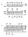
次に、図6を参照して工程(b)を説明する。
工程(b)は、工程(a)で得られた、有機EL素子または色変換フィルタ基板のいずれか一方に隔壁124を設ける工程である。Next, a process (b) is demonstrated with reference to FIG.
Step (b) is a step of providing
図6(a)はTFT型の有機EL素子に隔壁を設けた場合の図である。また、図6(b)はパッシブマトリックス型の有機EL素子に隔壁を設けた場合の図である。図6(c)は、色変換フィルタ基板に隔壁を設けた場合の図である。 FIG. 6A is a diagram in the case where a partition wall is provided in a TFT type organic EL element. FIG. 6B is a diagram in the case where a partition is provided in a passive matrix type organic EL element. FIG. 6C is a diagram in the case where a partition wall is provided on the color conversion filter substrate.
これらの図に示されるように、隔壁124は、有機EL素子上のサブピクセル間、または色変換フィルタ基板上のサブピクセル間(色変換フィルタ層の設けられていない部分)に形成される。 As shown in these drawings, the
隔壁124は、例えば上述のような光反射性または光散乱性の微粉末を含むレジスト材料をスピンコート法のような手段で成膜し、フォトリソグラフィー法を適用してパターンニングを行うことにより形成される。また、大画素であればスクリーン印刷のような印刷手段により形成することもできる。 The
本発明では、有機EL素子または色変換フィルタ基板のいずれか一方に隔壁124を設ければよい。 In the present invention, the
工程(c)は、得られた有機EL素子と色変換フィルタ基板を貼り合わせる工程である。 Step (c) is a step of bonding the obtained organic EL element and the color conversion filter substrate together.
具体的には、上記のように形成したTFT型またはパッシブマトリックス型有機EL素子と色変換フィルタ基板を乾燥窒素雰囲気(望ましくは、酸素および水分濃度ともに1ppm以下)内に配置する。そして、ディスペンサーロボットを用いて外周部に紫外線硬化型接着剤を塗布する。その後に、有機EL素子と色変換フィルタ基板とを密着させる。続いて、有機EL素子の発光部と色変換フィルタ層とのアライメントを行う。アクティブマトリクス駆動の場合には、下部電極と色変換フィルタ層との位置合わせを行う。一方、パッシブマトリクス駆動の場合には、下部電極および上部電極のラインパターンの交差部分と色変換フィルタ層との位置合わせを行う。 Specifically, the TFT type or passive matrix type organic EL element formed as described above and the color conversion filter substrate are placed in a dry nitrogen atmosphere (desirably, oxygen and moisture concentrations are both 1 ppm or less). And an ultraviolet curable adhesive is apply | coated to an outer peripheral part using a dispenser robot. Thereafter, the organic EL element and the color conversion filter substrate are brought into close contact with each other. Subsequently, the light emitting portion of the organic EL element and the color conversion filter layer are aligned. In the case of active matrix driving, the lower electrode and the color conversion filter layer are aligned. On the other hand, in the case of passive matrix driving, the color conversion filter layer is aligned with the intersection of the line pattern of the lower electrode and the upper electrode.
その後に、前述の紫外線硬化型接着剤に対して紫外線を照射して、該接着剤を硬化させて外周封止層120を形成する。紫外線照射は、例えば100mW/cm2の照度で30秒間にわたって行うことが好ましい。After that, the outer
本工程では、図7(a)に示されるように、隔壁124を有機EL素子に設けた場合は、色変換フィルタ基板と隔壁を設けた有機EL素子を貼り合わせる。貼り合わせに際し、外周封止層120および充填剤層126を設けた(図7(b))。また、図8(a)に示されるように色変換フィルタ基板に隔壁を設けた場合は、隔壁を設けた色変換フィルタ基板と有機EL素子を貼り合わせる。貼り合わせに際し、外周封止層120および充填剤層126を設けた(図8(b))。
以上のようにして、カラー有機EL素子を形成することができる。In this step, as shown in FIG. 7A, when the
As described above, a color organic EL element can be formed.
(実施例)
(実施例1)
従来から知られた手法により、ガラス基板上に、TFTをパターン形成した。次いで、下部電極であるIZOを、DCスパッタガスとしてArを用いたスパッタリングにより100nm積層した。この後、有機蒸着装置で正孔注入層として厚さ40nmのαNPDを、有機発光層として厚さ60nmのアルミキレート(Alq3)を、電子注入層として、厚さ1nmのLiを積層した。次に、DCスパッタリング法により上部の透明電極であるIZOを形成した。IZOの成膜条件は、スパッタガスにはArを用い、ターゲットにはIZOを用いた。この後、形成した各層を覆うように、従来の手順に従いパッシベーション層を形成した。(Example)
(Example 1)
A TFT was patterned on a glass substrate by a conventionally known method. Next, IZO, which is the lower electrode, was deposited to a thickness of 100 nm by sputtering using Ar as a DC sputtering gas. Thereafter, αNPD having a thickness of 40 nm was stacked as a hole injection layer by an organic vapor deposition apparatus, aluminum chelate (Alq3) having a thickness of 60 nm was stacked as an organic light emitting layer, and Li having a thickness of 1 nm was stacked as an electron injection layer. Next, IZO, which is the upper transparent electrode, was formed by DC sputtering. The film formation conditions for IZO were Ar for the sputtering gas and IZO for the target. Thereafter, a passivation layer was formed according to a conventional procedure so as to cover each formed layer.
[隔壁の形成]
得られた有機EL素子上に、隔壁を形成した。隔壁はSrOの吸湿性白色微粉末を含むレジスト材料(ZPN1100(日本ゼオン製))をスピンコート法などで塗布し、フォトリソグラフィー法を適用してパターンニングすることにより形成した。なお、SrOとレジスト材料の混合割合は、重量比で5:1であった。[Partition formation]
A partition wall was formed on the obtained organic EL element. The partition walls were formed by applying a resist material (ZPN1100 (manufactured by Zeon Japan)) containing hygroscopic white fine powder of SrO by spin coating and patterning by applying a photolithography method. The mixing ratio of SrO and resist material was 5: 1 by weight.
このようにして得られた、隔壁を有するTFT型有機EL素子に、以下の色変換フィルタ基板を貼り合わせ、カラー有機EL素子を作製した。本実施例では、長辺方向のピッチ195μm、短辺方向のピッチ65μmを有して、陽極を配置した。各陽極と陰極が対向するエリアの寸法は、長辺方向180μm、短辺方向50μmであった。 The following color conversion filter substrate was bonded to the TFT-type organic EL element having the partition walls obtained in this manner, to produce a color organic EL element. In this example, the anode was arranged with a pitch of 195 μm in the long side direction and a pitch of 65 μm in the short side direction. The dimensions of the area where each anode and cathode face each other were 180 μm in the long side direction and 50 μm in the short side direction.
[色変換フィルタ基板の作製]
下記要領で、青色フィルタ、緑色変換フィルタ、赤色変換フィルタおよび平坦化層の作製で説明した手順に従い、透明な基板上に各層を形成し、色変換フィルタ基板を形成した。各カラーフィルタ層および蛍光変換層は、48×178μmの寸法を有した。[Production of color conversion filter substrate]
In the following manner, each layer was formed on a transparent substrate according to the procedure described in the preparation of the blue filter, the green conversion filter, the red conversion filter, and the planarization layer, thereby forming a color conversion filter substrate. Each color filter layer and fluorescence conversion layer had a size of 48 × 178 μm.
[青色フィルタの作製]
青色フィルタ材料(富士フィルムアーチ社製、カラーモザイクCB−7001)を、透明基板としてのコーニングガラス(50×50×1.1mm)上にスピンコート法により塗布し、フォトリソグラフィー法によりパターンニングを実施して青色フィルタを得た。[Production of blue filter]
A blue filter material (Fuji Film Arch Co., Ltd., Color Mosaic CB-7001) is applied on a coning glass (50 x 50 x 1.1 mm) as a transparent substrate by spin coating, and patterning is performed by photolithography. A blue filter was obtained.
[緑色変換フィルタの作製]
蛍光色素としてクマリン(0.7重量部)を溶剤のプロピレングリコールモノエチルアセテート(PGMEA)(120重量部)へ溶解させた。これに光重合性樹脂V259PA/P5(商品名、新日鐵化学(株))(100重量部)を加えて溶解させ、塗布液を得た。この塗布液を、青色フィルタのラインパターンが形成された透明基板上にスピンコート法を用いて塗布し、フォトリソグラフ法によりパターンニングを実施して緑色変換フィルタを得た。[Production of green conversion filter]
Coumarin (0.7 parts by weight) as a fluorescent dye was dissolved in propylene glycol monoethyl acetate (PGMEA) (120 parts by weight) as a solvent. A photopolymerizable resin V259PA / P5 (trade name, Nippon Steel Chemical Co., Ltd.) (100 parts by weight) was added thereto and dissolved to obtain a coating solution. This coating solution was applied onto a transparent substrate on which a blue filter line pattern was formed by using a spin coating method, and was patterned by a photolithographic method to obtain a green conversion filter.
[赤色変換フィルタの作製]
蛍光色素としてクマリン(0.6重量部)、ローダミン6G(0.3重量部)、ベーシックバイオレット11(0.3重量部)を溶剤のプロピレングリコールモノエチルアセテート(PGMEA)(120重量部)へ溶解させた。これに光重合性樹脂V259PA/P5(商品名、新日鐵化学(株))(100重量部)を加えて溶解させ、塗布液を得た。この塗布液を、青色フィルタおよび緑色変換フィルタのラインパターンが形成された透明基板上にスピンコート法を用いて塗布し、フォトリソグラフ法によりパターンニングを実施して赤色変換フィルタを得た。[Production of red conversion filter]
Coumarin (0.6 parts by weight), rhodamine 6G (0.3 parts by weight) and basic violet 11 (0.3 parts by weight) as fluorescent dyes are dissolved in propylene glycol monoethyl acetate (PGMEA) (120 parts by weight) as a solvent. I let you. A photopolymerizable resin V259PA / P5 (trade name, Nippon Steel Chemical Co., Ltd.) (100 parts by weight) was added thereto and dissolved to obtain a coating solution. This coating solution was applied onto a transparent substrate on which a line pattern of a blue filter and a green conversion filter was formed by using a spin coating method, and patterning was performed by a photolithographic method to obtain a red conversion filter.
「オーバーコート層およびパッシベーション層の形成]
i)オーバーコート層の作製
上記の工程で作製された蛍光変換フィルタ上に、UV硬化型樹脂(エポキシ変性アクリレート)をスピンコート法により塗布し、高圧水銀灯で照射して膜厚8μmのオーバーコート層を形成した。オーバーコート層を形成した後の蛍光変換フィルタのパターンは変形していなかった。また、オーバーコート層の上面は平坦であった。“Formation of overcoat layer and passivation layer”
i) Production of overcoat layer On the fluorescence conversion filter produced in the above process, a UV curable resin (epoxy-modified acrylate) is applied by a spin coat method, and irradiated with a high-pressure mercury lamp to form an overcoat layer having a thickness of 8 μm. Formed. The pattern of the fluorescence conversion filter after forming the overcoat layer was not deformed. The upper surface of the overcoat layer was flat.
ii)パッシベーション層の作製
無機膜層として、DCスパッタ法により、室温において、膜厚300nmのSiOx膜を形成した。スパッタターゲットにはSiを用い、スパッタガスとしてArおよび酸素の混合ガス(Ar:酸素=5:1)を使用した。ii) Preparation of Passivation Layer A 300-nm thick SiOx film was formed at room temperature as the inorganic film layer by DC sputtering. Si was used as the sputtering target, and a mixed gas of Ar and oxygen (Ar: oxygen = 5: 1) was used as the sputtering gas.
[貼り合わせ工程]
上述のように形成された有機EL素子と色変換フィルタ基板を、グローブボックス内で、乾燥窒素雰囲気下(酸素および水分濃度共に1ppm以下)においてUV硬化接着剤を用いて貼り合わせ、封止した。[Lamination process]
The organic EL element and the color conversion filter substrate formed as described above were bonded and sealed using a UV curable adhesive in a glove box under a dry nitrogen atmosphere (both oxygen and moisture concentrations were 1 ppm or less).
(実施例2)
ガラス基板上にDCスパッタリングにより100nmのCrB(反射膜)を形成した。スパッタガスとしてArを用い300Wのパワーを印加した。さらに下部電極であるIZOを、DCスパッタガスとしてArを用いたスパッタリングにより100nm積層し、フォトリソグラフ法によりパターンニングを施した。この後、有機蒸着装置で正孔注入層として厚さ40nmのαNPDを、有機発光層として厚さ60nmのアルミキレート(Alq3)を、電子注入層として、厚さ1nmのLiを積層した。次に、DCスパッタリング法により上部の透明電極であるIZOを形成し、下部電極と垂直の方向にパターンニングを施した。上部電極(IZO)の成膜条件は、スパッタガスにはArを用い、ターゲットにはIZOを用いた。これに実施例1と同様の手順で、隔壁を形成し、実施例1で説明した色変換フィルタ基板を貼り合わせ、カラー有機ELディスプレイを作製した。(Example 2)
A 100 nm CrB (reflection film) was formed on the glass substrate by DC sputtering. A power of 300 W was applied using Ar as the sputtering gas. Further, IZO, which is the lower electrode, was deposited to a thickness of 100 nm by sputtering using Ar as a DC sputtering gas, and was patterned by a photolithographic method. Thereafter, αNPD having a thickness of 40 nm was stacked as a hole injection layer by an organic vapor deposition apparatus, aluminum chelate (Alq3) having a thickness of 60 nm was stacked as an organic light emitting layer, and Li having a thickness of 1 nm was stacked as an electron injection layer. Next, IZO, which is an upper transparent electrode, was formed by DC sputtering, and patterning was performed in a direction perpendicular to the lower electrode. The film formation conditions for the upper electrode (IZO) were Ar for the sputtering gas and IZO for the target. In the same procedure as in Example 1, partition walls were formed, and the color conversion filter substrate described in Example 1 was bonded to produce a color organic EL display.
(実施例3)
実施例1に示した方法により、TFT型の有機EL素子を作成した。次に実施例1に示した方法により色変換フィルタ基板を作成した。この色変換フィルタ基板上に隔壁を形成した。隔壁はSrOの吸湿性白色微粉末を含むレジスト材料(ZPN1100(日本ゼオン製))をスピンコート法などで塗布し、フォトリソグラフィー法を適用してパターンニングすることにより形成した。なお、SrOとレジスト材料の混合割合は、重量比で5:1であった。(Example 3)
By the method shown in Example 1, a TFT type organic EL device was prepared. Next, a color conversion filter substrate was prepared by the method shown in Example 1. A partition wall was formed on the color conversion filter substrate. The partition walls were formed by applying a resist material (ZPN1100 (manufactured by Zeon Japan)) containing hygroscopic white fine powder of SrO by spin coating and patterning by applying a photolithography method. The mixing ratio of SrO and resist material was 5: 1 by weight.
隔壁を有する色変換フィルタ基板とTFT型の有機EL素子をグローブボックス内で、乾燥窒素雰囲気下(酸素および水分濃度共に1ppm以下)においてUV硬化接着剤を用いて貼り合わせ、封止した。 A color conversion filter substrate having a partition wall and a TFT type organic EL element were bonded and sealed in a glove box using a UV curable adhesive in a dry nitrogen atmosphere (both oxygen and moisture concentrations were 1 ppm or less).
(比較例1、2、3)
隔壁を形成しないことをのぞいて実施例1、2および3と同様にしてカラー有機ELディスプレイを形成した。(Comparative Examples 1, 2, 3)
A color organic EL display was formed in the same manner as in Examples 1, 2, and 3 except that no partition wall was formed.
(評価)
カラー有機ELディスプレイの評価を以下の通り行った。(Evaluation)
The color organic EL display was evaluated as follows.
(発光効率試験)
上記各実施例および比較例の有機EL素子を100cd/m2の輝度で点灯させ、その際の電流を測定して電流効率の相対値を求めることにより評価した。結果を表1に示す。いずれの実施例共に比較例に対して高い発光効率を示した。(Luminescence efficiency test)
The organic EL elements of the above examples and comparative examples were lit at a luminance of 100 cd / m2 , and the current at that time was measured to obtain a relative value of current efficiency. The results are shown in Table 1. Both examples showed higher luminous efficiency than the comparative example.

(耐久試験)
本発明のカラー有機ELディスプレイの長期安定性を試験するため、室温で1000時間の駆動試験を行い、ダークスポットの発生の有無を試験した。結果を表2に示す。(An endurance test)
In order to test the long-term stability of the color organic EL display of the present invention, a driving test was performed at room temperature for 1000 hours to test whether dark spots were generated. The results are shown in Table 2.
10、20 カラー有機ELディスプレイ
102 支持基板
104 下部電極
106 上部電極
108 ブラックマトリックス
110 色変換層
112 平坦化層
114a、114b パッシベーション層
116 有機発光層
118 透明基板
120 外周封止層
122 TFT
124 隔壁
126 充填剤層
128 オーバーコート層
10, 20 Color
124
Claims (4)
Translated fromJapanese(a)有機EL素子と色変換フィルタ基板を提供する工程と、
(b)前記有機EL素子上または前記色変換フィルタ基板上のいずれか一方に光散乱性または光反射性である隔壁を形成する工程と、
(c)有機EL素子に隔壁を形成した場合には、色変換フィルタと隔壁を形成した有機EL素子とを貼り合わせ、色変換フィルタ基板に隔壁を形成した場合には、隔壁を形成した色変換フィルタ基板と有機EL素子とを貼り合わせる工程とを含むことを特徴とするカラー有機ELディスプレイの製造方法。A method for producing a color organic EL display,
(A) providing an organic EL element and a color conversion filter substrate;
(B) forming a light-scattering or light-reflecting partition on either the organic EL element or the color conversion filter substrate;
(C) When a partition wall is formed on the organic EL element, the color conversion filter and the organic EL element on which the partition wall is formed are bonded together, and when the partition wall is formed on the color conversion filter substrate, the color conversion with the partition wall is formed. A method for producing a color organic EL display, comprising a step of bonding a filter substrate and an organic EL element.
Priority Applications (1)
| Application Number | Priority Date | Filing Date | Title |
|---|---|---|---|
| JP2003358320AJP2005123089A (en) | 2003-10-17 | 2003-10-17 | Color organic EL display and manufacturing method thereof |
Applications Claiming Priority (1)
| Application Number | Priority Date | Filing Date | Title |
|---|---|---|---|
| JP2003358320AJP2005123089A (en) | 2003-10-17 | 2003-10-17 | Color organic EL display and manufacturing method thereof |
Publications (1)
| Publication Number | Publication Date |
|---|---|
| JP2005123089Atrue JP2005123089A (en) | 2005-05-12 |
Family
ID=34614924
Family Applications (1)
| Application Number | Title | Priority Date | Filing Date |
|---|---|---|---|
| JP2003358320APendingJP2005123089A (en) | 2003-10-17 | 2003-10-17 | Color organic EL display and manufacturing method thereof |
Country Status (1)
| Country | Link |
|---|---|
| JP (1) | JP2005123089A (en) |
Cited By (29)
| Publication number | Priority date | Publication date | Assignee | Title |
|---|---|---|---|---|
| JP2007157404A (en)* | 2005-12-01 | 2007-06-21 | Seiko Epson Corp | Display device and electronic device |
| JP2007200887A (en)* | 2006-01-25 | 2007-08-09 | Samsung Sdi Co Ltd | Organic electroluminescent display device and manufacturing method thereof |
| JP2007234310A (en)* | 2006-02-28 | 2007-09-13 | Fuji Electric Holdings Co Ltd | Manufacturing method and manufacturing apparatus for organic EL display |
| JP2008059868A (en)* | 2006-08-30 | 2008-03-13 | Seiko Epson Corp | ORGANIC ELECTROLUMINESCENT DEVICE, ITS MANUFACTURING METHOD, AND ELECTRONIC DEVICE |
| WO2008102694A1 (en)* | 2007-02-21 | 2008-08-28 | Ulvac, Inc. | Display device, apparatus for manufacturing display device, and method for manufacturing display device |
| JP2009503780A (en)* | 2005-07-29 | 2009-01-29 | サエス ゲッタース ソチエタ ペル アツィオニ | Getter system comprising an adhesion layer of one or more getter materials and a layer of material for H2O transfer |
| WO2010004865A1 (en)* | 2008-07-10 | 2010-01-14 | 富士電機ホールディングス株式会社 | Organic el display and method for manufacturing same |
| JP2010118273A (en)* | 2008-11-13 | 2010-05-27 | Sony Corp | Display |
| US7825594B2 (en) | 2006-01-25 | 2010-11-02 | Samsung Mobile Display Co., Ltd. | Organic light emitting display and fabricating method of the same |
| JP2010272214A (en)* | 2009-05-19 | 2010-12-02 | Fuji Electric Holdings Co Ltd | Color conversion type organic EL display |
| US7944143B2 (en) | 2006-01-25 | 2011-05-17 | Samsung Mobile Display Co., Ltd. | Organic light-emitting display device with frit seal and reinforcing structure bonded to frame |
| US8038495B2 (en) | 2006-01-20 | 2011-10-18 | Samsung Mobile Display Co., Ltd. | Organic light-emitting display device and manufacturing method of the same |
| US8063561B2 (en) | 2006-01-26 | 2011-11-22 | Samsung Mobile Display Co., Ltd. | Organic light emitting display device |
| US8120249B2 (en) | 2006-01-23 | 2012-02-21 | Samsung Mobile Display Co., Ltd. | Organic light emitting display and method of fabricating the same |
| US8125146B2 (en) | 2006-01-27 | 2012-02-28 | Samsung Mobile Display Co., Ltd. | Organic light emitting display having a second frit portion configured to melt more easily than a frit portion |
| WO2012063700A1 (en)* | 2010-11-11 | 2012-05-18 | シャープ株式会社 | Light diffusing plate, organic electroluminescent display device, and electronic apparatus |
| WO2012081568A1 (en)* | 2010-12-16 | 2012-06-21 | シャープ株式会社 | Fluorescent substrate, display device, and lighting device |
| US8299705B2 (en) | 2006-01-26 | 2012-10-30 | Samsung Display Co., Ltd. | Organic light emitting display device and manufacturing method thereof |
| WO2013039072A1 (en)* | 2011-09-16 | 2013-03-21 | シャープ株式会社 | Light-emitting device, display apparatus, illumination apparatus, and electricity-generating apparatus |
| US8415880B2 (en) | 2006-01-20 | 2013-04-09 | Samsung Display Co., Ltd. | Organic light-emitting display device with frit seal and reinforcing structure |
| JP2013069480A (en)* | 2011-09-21 | 2013-04-18 | Semiconductor Energy Lab Co Ltd | Light-emitting device, electronic equipment, and illuminating device |
| WO2013118510A1 (en)* | 2012-02-08 | 2013-08-15 | パナソニック株式会社 | Organic electroluminescent light emitting device and method for manufacturing same |
| JP2014160644A (en)* | 2013-02-19 | 2014-09-04 | Au Optronics Corp | Color light emitting diode, display panel and method for manufacturing the same |
| WO2014091010A3 (en)* | 2012-12-13 | 2014-09-18 | Osram Opto Semiconductors Gmbh | Organic, electronic component and method for producing an organic, electronic component |
| JP2015050059A (en)* | 2013-09-02 | 2015-03-16 | 株式会社ジャパンディスプレイ | Display device |
| US9161397B2 (en) | 2012-10-10 | 2015-10-13 | Rohm Co., Ltd. | Organic EL device |
| KR101747268B1 (en)* | 2015-11-30 | 2017-06-14 | 엘지디스플레이 주식회사 | Organic light emitting display device and head mounted display including the same |
| US20190165316A1 (en)* | 2017-11-29 | 2019-05-30 | Lg Display Co., Ltd. | Display Device |
| CN110908168A (en)* | 2018-09-14 | 2020-03-24 | 三星显示有限公司 | display screen |
- 2003
- 2003-10-17JPJP2003358320Apatent/JP2005123089A/enactivePending
Cited By (46)
| Publication number | Priority date | Publication date | Assignee | Title |
|---|---|---|---|---|
| JP2009503780A (en)* | 2005-07-29 | 2009-01-29 | サエス ゲッタース ソチエタ ペル アツィオニ | Getter system comprising an adhesion layer of one or more getter materials and a layer of material for H2O transfer |
| US8911862B2 (en) | 2005-07-29 | 2014-12-16 | Saes Getters S.P.A. | Getter systems comprising one or more deposits of getter material and a layer of material for the transport of water |
| JP2007157404A (en)* | 2005-12-01 | 2007-06-21 | Seiko Epson Corp | Display device and electronic device |
| US9004972B2 (en) | 2006-01-20 | 2015-04-14 | Samsung Display Co., Ltd. | Organic light-emitting display device with frit seal and reinforcing structure |
| US8415880B2 (en) | 2006-01-20 | 2013-04-09 | Samsung Display Co., Ltd. | Organic light-emitting display device with frit seal and reinforcing structure |
| US8038495B2 (en) | 2006-01-20 | 2011-10-18 | Samsung Mobile Display Co., Ltd. | Organic light-emitting display device and manufacturing method of the same |
| US8120249B2 (en) | 2006-01-23 | 2012-02-21 | Samsung Mobile Display Co., Ltd. | Organic light emitting display and method of fabricating the same |
| US7944143B2 (en) | 2006-01-25 | 2011-05-17 | Samsung Mobile Display Co., Ltd. | Organic light-emitting display device with frit seal and reinforcing structure bonded to frame |
| JP2007200887A (en)* | 2006-01-25 | 2007-08-09 | Samsung Sdi Co Ltd | Organic electroluminescent display device and manufacturing method thereof |
| US7825594B2 (en) | 2006-01-25 | 2010-11-02 | Samsung Mobile Display Co., Ltd. | Organic light emitting display and fabricating method of the same |
| US8299705B2 (en) | 2006-01-26 | 2012-10-30 | Samsung Display Co., Ltd. | Organic light emitting display device and manufacturing method thereof |
| US8063561B2 (en) | 2006-01-26 | 2011-11-22 | Samsung Mobile Display Co., Ltd. | Organic light emitting display device |
| US8125146B2 (en) | 2006-01-27 | 2012-02-28 | Samsung Mobile Display Co., Ltd. | Organic light emitting display having a second frit portion configured to melt more easily than a frit portion |
| JP2007234310A (en)* | 2006-02-28 | 2007-09-13 | Fuji Electric Holdings Co Ltd | Manufacturing method and manufacturing apparatus for organic EL display |
| JP2008059868A (en)* | 2006-08-30 | 2008-03-13 | Seiko Epson Corp | ORGANIC ELECTROLUMINESCENT DEVICE, ITS MANUFACTURING METHOD, AND ELECTRONIC DEVICE |
| US7857673B2 (en) | 2007-02-21 | 2010-12-28 | Ulvac, Inc. | Display device, apparatus for producing display device, and method for producing display device |
| WO2008102694A1 (en)* | 2007-02-21 | 2008-08-28 | Ulvac, Inc. | Display device, apparatus for manufacturing display device, and method for manufacturing display device |
| WO2010004865A1 (en)* | 2008-07-10 | 2010-01-14 | 富士電機ホールディングス株式会社 | Organic el display and method for manufacturing same |
| KR101209128B1 (en) | 2008-07-10 | 2012-12-06 | 샤프 가부시키가이샤 | Organic el display and method for manufacturing same |
| US8629614B2 (en) | 2008-07-10 | 2014-01-14 | Sharp Kabushiki Kaisha | Organic EL display and method for manufacturing same |
| JP2010118273A (en)* | 2008-11-13 | 2010-05-27 | Sony Corp | Display |
| JP2010272214A (en)* | 2009-05-19 | 2010-12-02 | Fuji Electric Holdings Co Ltd | Color conversion type organic EL display |
| WO2012063700A1 (en)* | 2010-11-11 | 2012-05-18 | シャープ株式会社 | Light diffusing plate, organic electroluminescent display device, and electronic apparatus |
| WO2012081568A1 (en)* | 2010-12-16 | 2012-06-21 | シャープ株式会社 | Fluorescent substrate, display device, and lighting device |
| WO2013039072A1 (en)* | 2011-09-16 | 2013-03-21 | シャープ株式会社 | Light-emitting device, display apparatus, illumination apparatus, and electricity-generating apparatus |
| JP2013069480A (en)* | 2011-09-21 | 2013-04-18 | Semiconductor Energy Lab Co Ltd | Light-emitting device, electronic equipment, and illuminating device |
| WO2013118510A1 (en)* | 2012-02-08 | 2013-08-15 | パナソニック株式会社 | Organic electroluminescent light emitting device and method for manufacturing same |
| US9161397B2 (en) | 2012-10-10 | 2015-10-13 | Rohm Co., Ltd. | Organic EL device |
| WO2014091010A3 (en)* | 2012-12-13 | 2014-09-18 | Osram Opto Semiconductors Gmbh | Organic, electronic component and method for producing an organic, electronic component |
| JP2014160644A (en)* | 2013-02-19 | 2014-09-04 | Au Optronics Corp | Color light emitting diode, display panel and method for manufacturing the same |
| US9035286B2 (en) | 2013-02-19 | 2015-05-19 | Au Optronics Corporation | Multi-color light emitting diode and method for making same |
| JP2015050059A (en)* | 2013-09-02 | 2015-03-16 | 株式会社ジャパンディスプレイ | Display device |
| KR101747268B1 (en)* | 2015-11-30 | 2017-06-14 | 엘지디스플레이 주식회사 | Organic light emitting display device and head mounted display including the same |
| US10439167B2 (en) | 2015-11-30 | 2019-10-08 | Lg Display Co., Ltd. | Organic light emitting display device and head-mounted display including the same |
| KR20190063321A (en)* | 2017-11-29 | 2019-06-07 | 엘지디스플레이 주식회사 | Display Device |
| EP3493290A1 (en)* | 2017-11-29 | 2019-06-05 | LG Display Co., Ltd. | Display device |
| CN109841654A (en)* | 2017-11-29 | 2019-06-04 | 乐金显示有限公司 | Display device |
| US20190165316A1 (en)* | 2017-11-29 | 2019-05-30 | Lg Display Co., Ltd. | Display Device |
| US10673023B2 (en) | 2017-11-29 | 2020-06-02 | Lg Display Co., Ltd. | Display device |
| TWI696295B (en)* | 2017-11-29 | 2020-06-11 | 南韓商Lg顯示器股份有限公司 | Display device |
| KR102407978B1 (en)* | 2017-11-29 | 2022-06-13 | 엘지디스플레이 주식회사 | Display Device |
| CN109841654B (en)* | 2017-11-29 | 2023-09-15 | 乐金显示有限公司 | display device |
| CN110908168A (en)* | 2018-09-14 | 2020-03-24 | 三星显示有限公司 | display screen |
| KR20200031750A (en)* | 2018-09-14 | 2020-03-25 | 삼성디스플레이 주식회사 | Color filter and display device including the same |
| KR102572718B1 (en)* | 2018-09-14 | 2023-08-31 | 삼성디스플레이 주식회사 | Color filter and display device including the same |
| CN110908168B (en)* | 2018-09-14 | 2024-05-28 | 三星显示有限公司 | display screen |
Similar Documents
| Publication | Publication Date | Title |
|---|---|---|
| JP2005123089A (en) | Color organic EL display and manufacturing method thereof | |
| US7215075B2 (en) | Organic el device having upper electrode including plurality of transparent electrode layers and method for manufacturing the same | |
| JP3594018B2 (en) | Organic EL display | |
| US7182664B2 (en) | Method and an apparatus for manufacturing an organic EL display device | |
| JPWO2004036960A1 (en) | Organic electroluminescence display device and manufacturing method thereof | |
| JP2004207065A (en) | Color conversion light emitting device, method of manufacturing the same, and display using the device | |
| JP2007164123A (en) | Color filter with color conversion function, organic EL display, and manufacturing method thereof | |
| JP2008165108A (en) | Color filter substrate having rib function, color conversion filter substrate having rib function, color organic EL element using the same, and manufacturing method thereof | |
| JP2003243153A (en) | Organic EL display | |
| JP3726789B2 (en) | Organic EL display | |
| JP2008077943A (en) | Multicolor light emitting device | |
| JP4729754B2 (en) | Display device using a plurality of organic EL light emitting elements | |
| JP2004319143A (en) | Organic EL display and manufacturing method thereof | |
| JP2004103519A (en) | Color conversion color filter substrate and organic color display using the same | |
| JP4618562B2 (en) | Manufacturing method of organic EL display | |
| JP4419130B2 (en) | Manufacturing method of color conversion filter and color filter with color conversion function | |
| JP2005123088A (en) | Color conversion filter and organic EL display using the same | |
| JP2006278082A (en) | Full-color organic EL display device manufacturing method and optical processing device for manufacturing the same | |
| JP2003264081A (en) | Red fluorescence conversion filter and organic light emitting device using the same | |
| JP2009129586A (en) | Organic EL device | |
| JP4010286B2 (en) | Manufacturing method of organic EL display | |
| JP2012174334A (en) | Organic el panel and manufacturing method therefor | |
| JP2004227811A (en) | Organic EL display and manufacturing method thereof | |
| JP3861821B2 (en) | Organic EL display panel and manufacturing method thereof | |
| JP2007220431A (en) | Multicolor light emitting device and manufacturing method thereof |
Legal Events
| Date | Code | Title | Description |
|---|---|---|---|
| A621 | Written request for application examination | Free format text:JAPANESE INTERMEDIATE CODE: A621 Effective date:20060315 | |
| A977 | Report on retrieval | Free format text:JAPANESE INTERMEDIATE CODE: A971007 Effective date:20090303 | |
| A131 | Notification of reasons for refusal | Free format text:JAPANESE INTERMEDIATE CODE: A131 Effective date:20090306 | |
| A521 | Request for written amendment filed | Free format text:JAPANESE INTERMEDIATE CODE: A523 Effective date:20090416 | |
| A02 | Decision of refusal | Free format text:JAPANESE INTERMEDIATE CODE: A02 Effective date:20090901 |