JP2005085718A - Planar light emitting device - Google Patents
Planar light emitting deviceDownload PDFInfo
- Publication number
- JP2005085718A JP2005085718AJP2003319457AJP2003319457AJP2005085718AJP 2005085718 AJP2005085718 AJP 2005085718AJP 2003319457 AJP2003319457 AJP 2003319457AJP 2003319457 AJP2003319457 AJP 2003319457AJP 2005085718 AJP2005085718 AJP 2005085718A
- Authority
- JP
- Japan
- Prior art keywords
- light
- light emitting
- guide plate
- light guide
- emitting device
- Prior art date
- Legal status (The legal status is an assumption and is not a legal conclusion. Google has not performed a legal analysis and makes no representation as to the accuracy of the status listed.)
- Withdrawn
Links
Images
Landscapes
- Illuminated Signs And Luminous Advertising (AREA)
- Light Guides In General And Applications Therefor (AREA)
- Liquid Crystal (AREA)
- Planar Illumination Modules (AREA)
Abstract
Description
Translated fromJapanese本発明は面状発光装置に関する。詳しくは、発光素子の光を面状光に変換する面状発光装置に関する。 The present invention relates to a planar light emitting device. Specifically, the present invention relates to a planar light emitting device that converts light from a light emitting element into planar light.
発光素子の光を導光板によって面状の光に変換する面状発光装置が、液晶モニタや携帯電話のバックライトなど様々な用途に利用されている。このような面状発光装置では、導光板の端面に対向するように発光素子が配置され、発光素子の光は導光板の端面を介して導光板内へと取り込まれる。一般に、光の導入効率を高めるために発光素子は導光板の端面にできるだけ近接して配置される。しかし、いくら近接して発光素子を配置したとしても、入射面となる導光板端面が平面であるため、臨界角を越える光、即ち浅い入射角の光は入射の際に導光板端面で反射されてしまう。このような反射現象によって一部の光を有効に利用できず、十分な輝度の面状光を得られないという問題があった。
一方、特開2002−260423号公報(特許文献1)や特表2002−538577号公報(特許文献2)に開示される面状発光装置では、発光素子を導光板に組み込むことによって、上記のような導光板への導入の際に生ずる光のロスをなくし、光の利用効率を高めている。2. Description of the Related Art A planar light emitting device that converts light of a light emitting element into planar light by a light guide plate is used for various applications such as a liquid crystal monitor and a backlight of a mobile phone. In such a planar light emitting device, the light emitting element is disposed so as to face the end face of the light guide plate, and light of the light emitting element is taken into the light guide plate through the end face of the light guide plate. Generally, in order to increase the light introduction efficiency, the light emitting element is disposed as close as possible to the end face of the light guide plate. However, no matter how close the light emitting elements are arranged, the end face of the light guide plate serving as the entrance surface is flat, so that light exceeding the critical angle, that is, light having a shallow incident angle, is reflected by the end face of the light guide plate upon incidence. End up. Due to such a reflection phenomenon, part of the light cannot be used effectively, and there is a problem that planar light with sufficient luminance cannot be obtained.
On the other hand, in the planar light emitting device disclosed in Japanese Patent Application Laid-Open No. 2002-260423 (Patent Document 1) and Japanese Translation of PCT International Publication No. 2002-538577 (Patent Document 2), the light emitting element is incorporated into the light guide plate as described above. This eliminates the loss of light that occurs when it is introduced into a light guide plate, and increases the light utilization efficiency.
導光板内に発光素子を組み込むことにした場合であっても、発光素子の光は広がりを有することから、面状発光に有効に利用できる方向に向かって全ての光が進行することはなく、一部の光は発光に寄与できない。そこで本発明は、従来の構成では利用できないこのような光を有効に利用できる、光利用効率の高い面状発光装置を提供することを目的とする。 Even when it is decided to incorporate a light emitting element in the light guide plate, the light of the light emitting element has a spread, so that all the light does not travel in a direction that can be effectively used for planar light emission, Some light cannot contribute to light emission. Accordingly, an object of the present invention is to provide a planar light emitting device with high light utilization efficiency that can effectively use such light that cannot be used in the conventional configuration.
本発明は以上の目的を達成するために、以下の構成を提供する。即ち、
発光面を有する導光板と、
前記導光板の端部に埋入されている発光素子と、
前記端部の表面に密着した状態で備えられる反射面と、を備え、
前記端部の表面の少なくとも一部が、そこに到達する前記発光素子の光を前記反射面によって前記導光板の他端側へと反射できる二次又は高次曲面からなる、面状発光装置である。In order to achieve the above object, the present invention provides the following configurations. That is,
A light guide plate having a light emitting surface;
A light emitting device embedded in an end of the light guide plate;
A reflection surface provided in close contact with the surface of the end,
In the planar light emitting device, at least a part of the surface of the end portion is formed of a secondary or higher-order curved surface that can reflect the light of the light emitting element that reaches the other end side of the light guide plate by the reflecting surface. is there.
本発明では、発光素子が導光板の端部に埋入されていることから、発光素子の光は実質的なロスのない状態で導光板内へと導入される。しかも、発光素子から放出された光の中で、発光素子が配置される側の導光板端部の表面方向へ進行した光が、当該端部表面に設けられる反射面によって反射されて導光板の他端側へ向かう光に変換される。即ち、反射面の作用によって、導光板の他端側へと直接向かうことのできない光の外部漏出が防止されるとともに、良好な導光作用に寄与できる光が生ずる。このように、本発明の構成によれば、導光板への導入の際の光のロスが実質的にないことに加えて、導光板に導入された光のより多くを面状光に利用できることから高い光利用率を達成できる。 In the present invention, since the light emitting element is embedded in the end portion of the light guide plate, the light of the light emitting element is introduced into the light guide plate without substantial loss. In addition, among the light emitted from the light emitting element, the light traveling in the surface direction of the end portion of the light guide plate on the side where the light emitting element is disposed is reflected by the reflecting surface provided on the end surface and is reflected on the light guide plate. It is converted into light traveling toward the other end. That is, the action of the reflecting surface prevents the external leakage of light that cannot be directed directly to the other end of the light guide plate, and generates light that can contribute to a good light guide action. Thus, according to the configuration of the present invention, in addition to substantially no light loss when introduced into the light guide plate, more of the light introduced into the light guide plate can be used for planar light. High light utilization can be achieved.
本発明では導光体を板状に成形した導光板が使用される。典型的には平板状の導光板が使用されるが、平板状を基本として一部に凹凸を形成した形状や、一端側から他端側に向かって厚さが連続的又は段階的に変化する形状、或は略棒状の形状であってもよい。導光板には発光面が形成される。六面体からなる平板状の導光板を用いる場合を例に採れば、面積が最大の面のいずれか片方を発光面とすることができる。 In the present invention, a light guide plate in which a light guide is formed into a plate shape is used. Typically, a flat light guide plate is used, but the thickness changes continuously or stepwise from one end side to the other end side, or a shape with irregularities formed in part on the basis of a flat plate shape. It may be a shape or a substantially rod-like shape. A light emitting surface is formed on the light guide plate. Taking a case where a flat light guide plate made of hexahedron is used as an example, one of the surfaces with the largest area can be used as the light emitting surface.
導光板の端部(以下、「光導入部」ともいう)には後述の発光素子が埋入される。このように、本発明は導光板内に発光素子が直接組み込まれていることを一つの特徴とする。
導光板の光導入部の表面には、そこに密着した状態で反射面が備えられる。光導入部の表面の一部は、そこに到達する前記発光素子の光をこの反射面によって前記導光板の他端側へと反射できる二次又は高次曲面形状となっている。このような構成によって、発光素子の光の中で導光板の他端側へと進行せずに光導入部の表面方向へと進行した光の有効利用が図られる。A light emitting element to be described later is embedded in an end portion of the light guide plate (hereinafter also referred to as “light introducing portion”). Thus, the present invention is characterized in that the light emitting element is directly incorporated in the light guide plate.
The surface of the light introducing part of the light guide plate is provided with a reflecting surface in close contact therewith. A part of the surface of the light introducing portion has a secondary or higher order curved surface shape that can reflect the light of the light emitting element that reaches the light introducing portion to the other end side of the light guide plate by the reflection surface. With such a configuration, it is possible to effectively use the light that has traveled toward the surface of the light introducing portion without proceeding to the other end side of the light guide plate in the light of the light emitting element.
光導入部の具体的な形状としては例えば、発光素子の光軸を通り且つ導光板の発光面に垂直な断面において光導入部の外周が、部分放物線、部分楕円、若しくは部分双曲線、又はこれらの組み合わせによって規定されるものを挙げることができる。この中でも好ましいものとして部分放物線を挙げることができる。特に好ましい一態様として、本発明では上記のごとき断面における光導入部の外周が部分放物線となる光導入部(この場合には光導入部の外形が放物柱面又は放物面の一部を含むこととなる)が採用され、当該部分放物線の焦点位置に発光素子が配置される。この態様では光導入部の上に形成される反射面の作用によって、発光面に略平行な光を反射光として得ることが可能となる。このような反射光は導光板内を良好に導光し、最終的に得られる面状光の輝度上昇及び輝度ムラの軽減に寄与する。
尚、光導入部において一部を平坦な面としてもよい。例えば、後述の実施例に示すように光導入部の発光面側の外形を平面としてもよい。As a specific shape of the light introducing portion, for example, the outer periphery of the light introducing portion in a cross section passing through the optical axis of the light emitting element and perpendicular to the light emitting surface of the light guide plate is a partial parabola, a partial ellipse, a partial hyperbola, or these The thing prescribed | regulated by the combination can be mentioned. Among these, a partial parabola is preferable. As a particularly preferred embodiment, in the present invention, a light introducing portion in which the outer periphery of the light introducing portion in the cross section as described above is a partial parabola (in this case, the outer shape of the light introducing portion is a parabolic column surface or a part of a parabolic surface). The light emitting element is arranged at the focal position of the partial parabola. In this aspect, it is possible to obtain light substantially parallel to the light emitting surface as reflected light by the action of the reflecting surface formed on the light introducing portion. Such reflected light guides the inside of the light guide plate satisfactorily and contributes to an increase in luminance and reduction in luminance unevenness of the finally obtained planar light.
A part of the light introducing part may be a flat surface. For example, the outer shape on the light emitting surface side of the light introducing portion may be a flat surface as shown in the examples described later.
ここで、光源の光量が十分でない場合や、十分な導光作用が得られない場合などでは導光板内の光の分布にムラが生ずる惧れがある。例えば、光源から離れた領域で光量が低下し、その結果導光板の発光面から放射される光において輝度ムラが発生する惧れがある。このような場合には導光板の二箇所以上の端部に光導入部を設けてもよい。 Here, when the light amount of the light source is not sufficient, or when a sufficient light guiding effect cannot be obtained, there is a possibility that the light distribution in the light guide plate may be uneven. For example, the amount of light decreases in a region away from the light source, and as a result, there is a risk of uneven brightness in the light emitted from the light emitting surface of the light guide plate. In such a case, you may provide a light introduction part in the edge part of two or more places of a light-guide plate.
反射面は、光導入部の表面に密着した状態で形成される。かかる構成を採用することによって反射面による良好な反射作用が奏される。光導入部表面の全体に反射面を設け、光導入部から外部へと漏出する光の量をできるだけ少なくすることが好ましい。反射面は光反射性材料の蒸着や塗布などによって形成することができる。光反射性材料としては例えばAl、Agなどの金属材料を挙げることができるが、発光素子の光に対して反射率が高い材料であれば特にその種類は問わない。少なくとも貼付面が光反射性材料からなるテープやフィルム(例えば白色材料性のテープ)を光導入部の表面に貼付することによって反射面を形成してもよい。 The reflecting surface is formed in close contact with the surface of the light introducing portion. By adopting such a configuration, a good reflecting action by the reflecting surface is exhibited. It is preferable to provide a reflection surface on the entire surface of the light introducing portion so as to minimize the amount of light leaking from the light introducing portion to the outside. The reflective surface can be formed by vapor deposition or coating of a light reflective material. Examples of the light-reflective material include metal materials such as Al and Ag. However, the type of the light-reflective material is not particularly limited as long as the material has a high reflectance with respect to the light of the light-emitting element. You may form a reflective surface by sticking the tape or film (for example, white material-like tape) from which a sticking surface consists of a light-reflective material at least on the surface of a light introduction part.
光導入部以外の部分(但し発光面を除く)においても、その表面上に反射面を形成してもよい。例えば、発光面以外の表面を全て反射面で被覆してもよく、このようにすれば発光面以外からの光の漏出を防止でき、光の利用効率の上昇が期待できる。尚、反射面を設ければ光の反射作用のみならず光の拡散作用も生ずる。したがって、導光板内での光の拡散が促進され、もって発光面からより均一な光の放射が可能となる。 Also in a portion other than the light introducing portion (excluding the light emitting surface), a reflective surface may be formed on the surface. For example, the entire surface other than the light emitting surface may be covered with the reflecting surface. In this way, leakage of light from other than the light emitting surface can be prevented, and an increase in light utilization efficiency can be expected. If a reflecting surface is provided, not only the light reflecting action but also the light diffusing action occurs. Therefore, the diffusion of light within the light guide plate is promoted, so that more uniform light can be emitted from the light emitting surface.
以上のように発光素子が組み込まれた導光板は、インモールド成形によって簡便に作製することができる。具体的には、レンズ型LEDを作製するときと同様の要領で、所望の形状の金型を用意し、一端側に発光素子が封入されるようにして導光材料を硬化及び成形する。 The light guide plate in which the light emitting element is incorporated as described above can be easily manufactured by in-mold molding. Specifically, a mold having a desired shape is prepared in the same manner as when manufacturing a lens-type LED, and the light guide material is cured and molded so that the light emitting element is sealed on one end side.
導光板の材質は発光素子の光に対して透過性であれば特に限定されない。好ましくは透明(無色透明、有色透明を含む)な材料により導光板を構成する。また、加工が容易で耐久性に優れた材料により導光板を構成することが好ましい。導光板の材料としては例えば、アクリル樹脂、ポリエチレンテレフタレート(PET)、ポリカーボネート樹脂、エポキシ樹脂、ガラス等を用いることができる。 The material of the light guide plate is not particularly limited as long as it is transmissive to the light of the light emitting element. The light guide plate is preferably made of a transparent material (including colorless and transparent, and colored and transparent). Moreover, it is preferable to comprise a light-guide plate with the material which is easy to process and was excellent in durability. Examples of the material of the light guide plate include acrylic resin, polyethylene terephthalate (PET), polycarbonate resin, epoxy resin, and glass.
導光板の発光面又は裏面(発光面と表裏の関係にある面)の表面に凹凸部を形成することができる。このような凹凸部は、導光板内での光の拡散を促進することや、導光板内の配光を制御して発光面からの良好な光の放出を可能にすることなどに利用される。ここでの凹凸には三角溝、角溝、丸溝などの溝形状、及びピット形状などが含まれる。異なる形状の凹凸を複数組み合わせて用いても良い。このような凹凸を連続的に形成することもでき、またドット状など不連続的に形成することもできる。また、規則的に形成されていてもランダムに形成されていてもよい。
このような凹凸部は針状あるいは鋸歯状の加工具を用いて導光板の表面の一部を削り取ることや、導光板の表面にカッティング処理や研磨処理などを施すことにより形成することができる。または所望の凹凸部が形成されるような型を用いた型成形によって導光板を作製することによっても、このような凹凸部を形成することができる。An uneven part can be formed on the surface of the light emitting surface or the back surface of the light guide plate (the surface having the relationship between the light emitting surface and the front and back surfaces). Such uneven portions are used to promote the diffusion of light in the light guide plate, to control the light distribution in the light guide plate, and to allow good light emission from the light emitting surface. . The irregularities here include groove shapes such as triangular grooves, square grooves, and round grooves, and pit shapes. A plurality of uneven portions having different shapes may be used in combination. Such irregularities can be formed continuously, or can be formed discontinuously such as dots. Moreover, it may be formed regularly or randomly.
Such a concavo-convex part can be formed by scraping off a part of the surface of the light guide plate using a needle-like or saw-toothed processing tool, or by performing a cutting process or a polishing process on the surface of the light guide plate. Alternatively, such a concavo-convex portion can also be formed by producing a light guide plate by molding using a mold in which a desired concavo-convex portion is formed.
導光板にシリカなどの光拡散剤を含有させ、導光板内での光の拡散を促進させてもよい。光拡散剤を使用する場合には、発光素子から遠い領域ほど光拡散剤の含量が多くなるようにすることが好ましい。光の到達量が減少する領域において拡散効率が上昇し、輝度ムラが軽減されるからである。 A light diffusing agent such as silica may be included in the light guide plate to promote light diffusion in the light guide plate. When a light diffusing agent is used, it is preferable that the content of the light diffusing agent is increased in a region farther from the light emitting element. This is because diffusion efficiency increases in a region where the amount of light arrival decreases, and luminance unevenness is reduced.
導光板の裏面に光拡散層を形成することもできる。かかる光拡散層は、導光板内の光を発光面方向の光へと変換すること、及び導光板内の光の分布を均一化することを目的として形成される。輝度ムラの少ない光を発光面から放出するために、導光板裏面の実質的な全面に光拡散層を形成することが好ましい。但し、平面視において所定のパターンが形成されるように、導光板裏面の一部に光拡散層を形成することもできる。ここでのパターンとしては不規則的なものでもよいが、光拡散層全体に亘って均一な光の反射及び拡散を行い、これによって光放射面から輝度ムラのより少ない光を照射すべく、規則的なものを採用することが好ましい。規則的なパターンとしては所望の大きさのドットがマトリックス状に形成されるもの、スリット状のパターン、格子状のパターンなどを例示できる。 A light diffusion layer may be formed on the back surface of the light guide plate. Such a light diffusion layer is formed for the purpose of converting the light in the light guide plate into light in the direction of the light emitting surface and uniforming the light distribution in the light guide plate. In order to emit light with little luminance unevenness from the light emitting surface, it is preferable to form a light diffusion layer on substantially the entire back surface of the light guide plate. However, the light diffusion layer can be formed on a part of the rear surface of the light guide plate so that a predetermined pattern is formed in plan view. The pattern here may be irregular, but the light is uniformly reflected and diffused over the entire light diffusing layer, so that light with less luminance unevenness is emitted from the light emitting surface. It is preferable to adopt a typical one. Examples of the regular pattern include a pattern in which dots having a desired size are formed in a matrix, a slit pattern, a lattice pattern, and the like.
導光板の裏面に、光導入部から遠ざかるにつれて発光面側にテーパーする面を形成することができる。導光板の裏面全体をこのようなテーパー面とすることもできる。例えば、導光板の上端部を光導入部とする場合において導光板の裏面を、導光板の上端部から下端部に向かってテーパーする面とする。導光板の裏面をこのようなテーパー面とした場合において、例えば発光素子をその光軸が導光板発光面に平行となるように配置すれば、導光板裏面において光導入部からの距離が遠い領域でも光が到達しやすくなる。したがって、光導入部からの距離が遠くても受光量の低下が少なくなる。このように、発光面から放出される光の輝度分布がほぼ均一化されることとなる。 On the back surface of the light guide plate, a surface that tapers toward the light emitting surface as the distance from the light introducing portion increases can be formed. The entire back surface of the light guide plate may be a tapered surface. For example, when the upper end portion of the light guide plate is used as the light introducing portion, the back surface of the light guide plate is a surface that tapers from the upper end portion to the lower end portion of the light guide plate. In the case where the back surface of the light guide plate has such a tapered surface, for example, if the light emitting element is arranged so that the optical axis thereof is parallel to the light guide plate light emitting surface, the distance from the light introducing portion on the back surface of the light guide plate is long. But light is easy to reach. Therefore, the decrease in the amount of received light is reduced even when the distance from the light introducing portion is long. In this way, the luminance distribution of light emitted from the light emitting surface is substantially uniformed.
発光素子としては半導体発光素子(LED)が好適に使用される。LEDは消費電力及び発熱量が小さくかつ長寿命であることから、長時間連続的に点灯させることに適した光源である。また、小型であるため光源用のスペースが少なくてすみ、本発明の面状発光装置の小型化、薄型化が可能となる。これにより面状発光装置のハンドリング性も向上する。またLEDは振動、衝撃に強いことから、信頼性の高い面状発光装置を構成できるといった利点もある。
採用する光源の発光色も特に限定されず、白、赤、橙、緑、青等の可視領域の光を発光する光源を採用できる。好ましい光源としては、白色光を発光するものを挙げることができる。白色光を発光する光源を採用すれば、照明対象に表示された数字、文字、図形、バックグラウンドなどが本来の色で観察(視認)されるように構成できるからである。一方、白色以外の色の光源を用いれば、例えば照明対象を加色するなど、照明対象の意匠を変化させたり、意匠性を高めたりすることもできる。A semiconductor light emitting device (LED) is preferably used as the light emitting device. An LED is a light source suitable for lighting continuously for a long time because it has low power consumption and heat generation and has a long lifetime. Further, since the space is small, the space for the light source can be reduced, and the planar light emitting device of the present invention can be reduced in size and thickness. Thereby, the handleability of the planar light emitting device is also improved. Further, since the LED is resistant to vibration and impact, there is an advantage that a highly reliable planar light emitting device can be configured.
The light emission color of the light source to be employed is not particularly limited, and a light source that emits light in the visible region such as white, red, orange, green, and blue can be employed. As a preferable light source, one emitting white light can be cited. This is because if a light source that emits white light is employed, numbers, characters, figures, backgrounds, and the like displayed on the illumination target can be observed (viewed) in their original colors. On the other hand, if a light source of a color other than white is used, the design of the illumination target can be changed, for example, the color of the illumination target can be changed, or the design can be enhanced.
紫外領域の光を発光する光源を用いることもできる。この場合には、紫外領域の光を受けて蛍光する蛍光体を併せて用いることができる。尚、可視領域及び紫外領域の光を発光可能な発光素子を用いてもよい。
蛍光体を用いる場合には、例えば蛍光体を含む層を導光板表面(例えば発光面の表面)に設けることができる。このような蛍光体を含む層は蛍光体含有インク若しくは塗料の印刷、塗布などにより、又は蛍光体を含むシートの貼着などによって形成することができる。また、蛍光体を導光板内に含有させることができる。このような構成では導光板内で蛍光が生じ、この蛍光が導光板の発光面から放射することによって照明が行われる。蛍光体を導光板内に含有させる場合には、特に有機系の蛍光体を用いることが好ましい。有機系の蛍光体を用いれば導光板の透明性を維持でき、クリアー感のある照明効果が得られるからである。A light source that emits light in the ultraviolet region can also be used. In this case, a phosphor that receives light in the ultraviolet region and fluoresces can be used together. Note that a light-emitting element that can emit light in the visible region and the ultraviolet region may be used.
In the case of using a phosphor, for example, a layer containing the phosphor can be provided on the surface of the light guide plate (for example, the surface of the light emitting surface). Such a layer containing a phosphor can be formed by printing or applying a phosphor-containing ink or paint, or by attaching a sheet containing the phosphor. Moreover, a fluorescent substance can be contained in the light guide plate. In such a configuration, fluorescence is generated in the light guide plate, and illumination is performed by emitting this fluorescence from the light emitting surface of the light guide plate. In the case where the phosphor is contained in the light guide plate, it is particularly preferable to use an organic phosphor. This is because if the organic phosphor is used, the transparency of the light guide plate can be maintained, and a clear lighting effect can be obtained.
蛍光体の種類は特に限定されず、有機系、無機系を問わず採用することができる。有機系の蛍光体を用いることにより、上記のようにクリアー感のある蛍光色の光を得ることができる。他方、無機系の蛍光体を用いると、艶消し感のある蛍光色の光を得ることができる。様々な蛍光色を有する蛍光体を採用することができ、例えば光の三原色である赤色、緑色、又は青色の蛍光色を有する蛍光体の他、それらの中間色を蛍光する蛍光体を用いることができる。複数の蛍光体を組み合わせて用いることもでき、例えば赤色系蛍光体、緑色系蛍光体、及び青色系蛍光体を混合して用いることができる。 The kind of fluorescent substance is not specifically limited, It can employ | adopt regardless of an organic type and an inorganic type. By using an organic phosphor, it is possible to obtain fluorescent light with a clear feeling as described above. On the other hand, when an inorganic phosphor is used, fluorescent light with a matte feeling can be obtained. Phosphors having various fluorescent colors can be employed. For example, phosphors having fluorescent colors of red, green, or blue, which are the three primary colors of light, and phosphors that fluoresce their intermediate colors can be used. . A plurality of phosphors can be used in combination. For example, a red phosphor, a green phosphor, and a blue phosphor can be mixed and used.
本発明では必要に応じて複数個の発光素子が使用される。複数個の発光素子を使用する場合には、同種の発光素子を複数用いても、又は発光色などが異なる発光素子を組み合わせて用いてもよい。複数個の発光素子を用いることにより、発光面積のより広い面状発光装置を構成でき、また輝度の増強を図ることができる。尚、発光素子の使用数は、各発光素子の輝度、導光板の大きさ、必要な輝度等を総合的に考慮して定めることができる。
複数個の発光素子を用いる応用例として、赤色系LED、緑色系LED、青色系LEDの3種を用いて白色光を得る態様を挙げることができる。この態様では各LEDの発光状態、発光量を制御すれば、所望の色の面状光が得られる。
複数個の発光素子を用いる場合には例えば、導光板の光導入部において一端側から他端側に向かって一列に各発光素子が配置される。尚、複数の発光素子を用いる場合の配置態様は特に限定されるものではなく、面状発光装置に求められる発光態様を考慮して自由に設計できる。In the present invention, a plurality of light emitting elements are used as necessary. When a plurality of light emitting elements are used, a plurality of the same kind of light emitting elements may be used, or light emitting elements having different emission colors may be used in combination. By using a plurality of light emitting elements, a planar light emitting device having a wider light emitting area can be formed, and luminance can be enhanced. Note that the number of light emitting elements used can be determined by comprehensively considering the brightness of each light emitting element, the size of the light guide plate, the required brightness, and the like.
As an application example using a plurality of light emitting elements, an embodiment in which white light is obtained using three types of red LEDs, green LEDs, and blue LEDs can be given. In this aspect, planar light of a desired color can be obtained by controlling the light emission state and light emission amount of each LED.
When a plurality of light emitting elements are used, for example, the light emitting elements are arranged in a line from one end side to the other end side in the light introducing portion of the light guide plate. In addition, the arrangement | positioning aspect in the case of using a several light emitting element is not specifically limited, It can design freely in consideration of the light emission aspect calculated | required by the planar light-emitting device.
発光素子は、その光軸が所定の方向を向くように導光板内に配置される。例えば、導光板の発光面に光軸が略平行となるように発光素子を配置することができる。このように配置すれば良好な導光作用が得られる。後述の実施例に示すように、光導入部において導光板の裏面側方向に光軸が位置するように発光素子を配置してもよい。 The light emitting element is disposed in the light guide plate so that the optical axis thereof faces a predetermined direction. For example, the light emitting element can be arranged so that the optical axis is substantially parallel to the light emitting surface of the light guide plate. If it arrange | positions in this way, a favorable light guide effect will be acquired. As shown in the examples described later, the light emitting elements may be arranged so that the optical axis is positioned in the direction of the back surface of the light guide plate in the light introducing portion.
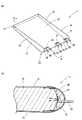
以下、実施例を用いて本発明の構成をより詳細に説明する。図1は本発明の実施例である面状発光装置1を示す図であって、図1aは面状発光装置1の斜視図、図1bは図1aのA−A線断面図である。面状発光装置1は例えば液晶モニタのバックライトに利用される。
面状発光装置1は導光板10及び発光素子構造20を備える。導光板10はアクリル樹脂製であって、略平板状の形状を有する。導光板10の一端部(光導入部11)には3つの発光素子構造20が埋入されている。導光板10の裏面13は、光導入部11側から他端14側に向かって次第に発光面12に近づくようにテーパーしている。尚、導光板10の発光面12及び裏面13は共に全体に渡って平坦な面である。
導光板10の光導入部11は部分放物柱形状に成形されている。詳細には、図1aにおけるA−A線位置での断面(図1b)においては、光導入部11の外形が放物線形状となる(外周が放物線によって規定されている)。光導入部11の表面、導光板裏面13の表面、及び導光板端面14の表面には、光反射率の高い金属の蒸着による反射面30が形成されている。一方、発光面12の表面は鏡面状となっている。Hereinafter, the configuration of the present invention will be described in more detail using examples. FIG. 1 is a diagram showing a planar light emitting device 1 according to an embodiment of the present invention, in which FIG. 1a is a perspective view of the planar light emitting device 1, and FIG. 1b is a cross-sectional view taken along line AA of FIG. The planar light emitting device 1 is used for a backlight of a liquid crystal monitor, for example.
The planar light emitting device 1 includes a
The
各発光素子構造20は、LED21、マウントフレーム22、及びリードフレーム23からなる。LED21は青色系の発光色を有するLEDである。LED21は、その光軸が導光板10の発光面12と平行でかつ導光板10の両側面15、16とも平行となる状態で、マウントフレーム22のカップ状部に載置・固定されている。尚、光導入部11の外形を規定する放物線の焦点位置にLED21が配置されるように、マウントフレーム22の位置が設定されている。
マウントフレーム22のカップ状部には黄色系の蛍光を発する蛍光体を分散させた光透過性樹脂25が充填されている。各LED21はマウントフレーム22及びリードフレーム23を介して給電される。尚、マウントフレーム22及びリードフレーム23は、図示しない回路基板に接続されている。Each light emitting
The cup-shaped portion of the
以上の構成の面状発光装置1では、LED21が点灯するとまず青色系の光が生ずる。この光の一部はLED21の周囲に存在する蛍光体の励起に利用され、黄色系の光を発生させる。これによって青色系の光と黄色系の光とが混色して得られる白色系の光が導光板10に導入されることとなる。導入光の中でその放射角度がLED21の光軸を基準として一定角度範囲内の光は、光導入部11が形成される側と反対側の導光板端部14側に向かって導光板10内を進行する。そして、放射角度に応じて一部の光は発光面12より直接外部に放射され、他の一部の光は導光板裏面13に至る。導光板裏面13に至った光は反射面30による反射作用を受け、発光面12方向の光へ変換される。これによって得られた光の中で一定の角度以上で発光面12に入射する光は発光面12を介して外部に取り出される。一方、発光面12への入射角度が十分でない光は発光面12による反射作用を受けて再び導光板裏面13方向の光となる。このような反射現象が繰り返された後、発光面12に対する入射角が一定の角度以上になった光から外部に取り出される。 In the planar light emitting device 1 having the above configuration, when the
一方、LED21の光軸方向から大きくずれて放出された光(横方向に放出された光)は光導入部11の表面方向へと進行し、光導入部11の表面に形成された反射面30によって反射される。上述のように、光導入部11の表面が放物柱面形状であって、この放物柱面形状を規定する放物線の焦点位置にLED21が配置されていることから、反射面30の作用によって生ずる反射光は、導光板発光面12に対して平行ないし平行に近いものとなり、導光板11内を良好に導光する。以上の作用によって、光の有効利用率が高まるとともに発光面12から放射される面状光の輝度の均一化が図られる。 On the other hand, light (light emitted in the lateral direction) emitted greatly deviating from the optical axis direction of the
ここで、導入光の一部は直接又は光導入部11での反射作用を受けた後に導光板裏面13に至るが、導光板裏面13上にも反射面30が形成されているため、ここでの光の漏出が防止される。同時に反射面30の反射・拡散作用によって、発光面12側へ向かう光の生成が良好に行われるとともに導光板10内での光密度分布が均一化され、高輝度かつ輝度ムラの少ない高品位の面状光が得られる。
また一方で導光板裏面13をテーパー面としたことから、光導入部11から離れた領域の導光板裏面13における受光量の増大、及び当該領域における光の取出効率の向上が図られ、もって発光面12から放出される面状光の輝度ムラが一層低減されることとなる。Here, a part of the introduced light reaches the light guide plate back
On the other hand, since the
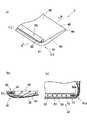
本発明の他の実施例を図2に示す。図2aは面状発光装置2の斜視図、図2bは図2aのB−B線断面図、図2cは図2aのC−C線断面図である。尚、上記図面における要素と同一の要素には同一の符号を付してその説明を省略する。上記の面状発光装置1と同様に、面状発光装置2も例えば液晶モニタのバックライトに利用される。
面状発光装置2は概略して導光板40及び光源50から構成される。導光板40はアクリル樹脂製であって、略平板状の形状を有する。導光板40の一端部(光導入部41)には光源50が組み込まれている。面状発光装置2では、光源50が組み込まれる側の面が発光面42となる。
導光板40の光導入部41は部分楕円柱形状に成形されている。詳細には、図2aにおけるB−B線位置での断面(図2b)においては、光導入部41の外形が、発光面42側から導光板裏面43側にかけて楕円形状となる(外周が楕円によって規定されている)。光導入部41において、光源50の端部50aに対向するエッジ部41aもまた、その断面形状が楕円によって規定される形状となっている(図2cを参照)。Another embodiment of the present invention is shown in FIG. 2a is a perspective view of the planar
The planar
The
光源50は、複数の発光素子部51とリフレクタ52とから構成される。リフレクタ52は棒状に成形された白色系樹脂からなり、その一面側には一条の溝が形成されている。この溝内に複数の発光素子部51が等間隔となるように一列に配置されている。各発光素子部51は三個のLED(赤系LED、緑系LED、青系LED)からなる。これらのLEDの光の混色によって各発光素子部51からは白色系の光が放出される。 The
以上の構成の面状発光装置2では、発光素子部51の各LEDが点灯すると、リフレクタ52の溝によって配光制御された白色光が放出される。この中で一部の光は、図2bに示すように、導光板裏面43側へと進行する。このような光の中で光導入部41の表面に至った光は反射面30の作用によって反射されることとなるが、上述のように光導入部41を楕円柱面状としたことから、導光板40の他端44側へ進行する光の生成が良好に行われる。一方、発光素子部51から放出された光の中で、リフレクタ52の溝に沿ってその長手方向に進行し、最終的にリフレクタ52の端部50aから放出される光は光導入部41のエッジ部41aに至る。ここで、当該エッジ部41aも楕円によって規定される外形とされていることから、ここにおいても図2cに示すように導光板他端44側へと進行する光が良好に生成する。
以上の各作用によって、光の有効利用率が高まるとともに発光面42から放射される面状光の輝度の均一化が図られる。In the planar
By the above actions, the effective utilization rate of light is increased and the luminance of the planar light emitted from the
尚、上記の面状発光装置1と同様に、導光板裏面43上などに形成された反射面30による反射・拡散作用が奏され、これによって高輝度かつ輝度ムラの少ない高品位の面状光が得られる。また面状発光装置1と同様に、光導入部41側から他端44側に向かって次第に発光面42に近づくように導光板裏面43がテーパーしており(図2bを参照)、これによって発光面42を介して放出される面状光の輝度ムラが一層低減されることとなる。 Similar to the planar light emitting device 1 described above, the reflection / diffusion action is exerted by the
この発明は、上記発明の実施の形態及び実施例の説明に何ら限定されるものではない。特許請求の範囲の記載を逸脱せず、当業者が容易に想到できる範囲で種々の変形態様もこの発明に含まれる。 The present invention is not limited to the description of the embodiments and examples of the invention described above. Various modifications may be included in the present invention as long as those skilled in the art can easily conceive without departing from the description of the scope of claims.
本発明の面状発光装置の適用対象(照明対象)としては例えば、PC(パーソナルコンピュータ)や携帯電話等の液晶モニタ、車両のライセンスプレート、屋外又は屋内で使用される指示板及び広告(板)等の情報伝達媒体、並びに書籍などを挙げることができる。尚、このような適用対象と本発明の面状発光装置とを一体的に構成することもできる。 As an application target (illumination target) of the planar light emitting device of the present invention, for example, a liquid crystal monitor such as a PC (personal computer) or a cellular phone, a license plate of a vehicle, an instruction board and an advertisement (board) used outdoors or indoors An information transmission medium such as, a book, and the like can be given. In addition, such an application object and the planar light emitting device of the present invention can also be configured integrally.
1、2 面状発光装置
10 40 導光板
11 41 光導入部
12 42 発光面
20 発光素子構造
21 LED
30 反射面
50 光源
51 発光素子部
52 リフレクタDESCRIPTION OF
30
Claims (5)
Translated fromJapanese前記導光板の端部に埋入されている発光素子と、
前記端部の表面に密着した状態で備えられる反射面と、を備え、
前記端部の表面の少なくとも一部が、そこに到達する前記発光素子の光を前記反射面によって前記導光板の他端側へと反射できる二次又は高次曲面からなる、面状発光装置。A light guide plate having a light emitting surface;
A light emitting device embedded in an end of the light guide plate;
A reflection surface provided in close contact with the surface of the end,
A planar light-emitting device, wherein at least a part of the surface of the end portion is formed of a secondary or higher-order curved surface that can reflect the light of the light emitting element that reaches the end to the other end side of the light guide plate by the reflecting surface.
Priority Applications (1)
| Application Number | Priority Date | Filing Date | Title |
|---|---|---|---|
| JP2003319457AJP2005085718A (en) | 2003-09-11 | 2003-09-11 | Planar light emitting device |
Applications Claiming Priority (1)
| Application Number | Priority Date | Filing Date | Title |
|---|---|---|---|
| JP2003319457AJP2005085718A (en) | 2003-09-11 | 2003-09-11 | Planar light emitting device |
Publications (1)
| Publication Number | Publication Date |
|---|---|
| JP2005085718Atrue JP2005085718A (en) | 2005-03-31 |
Family
ID=34418393
Family Applications (1)
| Application Number | Title | Priority Date | Filing Date |
|---|---|---|---|
| JP2003319457AWithdrawnJP2005085718A (en) | 2003-09-11 | 2003-09-11 | Planar light emitting device |
Country Status (1)
| Country | Link |
|---|---|
| JP (1) | JP2005085718A (en) |
Cited By (17)
| Publication number | Priority date | Publication date | Assignee | Title |
|---|---|---|---|---|
| WO2007013364A1 (en)* | 2005-07-27 | 2007-02-01 | Tohoku University | Backlight unit for liquid crystal display |
| US7826698B1 (en) | 2007-12-19 | 2010-11-02 | Oree, Inc. | Elimination of stitch artifacts in a planar illumination area |
| US7929816B2 (en) | 2007-12-19 | 2011-04-19 | Oree, Inc. | Waveguide sheet containing in-coupling, propagation, and out-coupling regions |
| US8128272B2 (en) | 2005-06-07 | 2012-03-06 | Oree, Inc. | Illumination apparatus |
| US8215815B2 (en) | 2005-06-07 | 2012-07-10 | Oree, Inc. | Illumination apparatus and methods of forming the same |
| US8231237B2 (en) | 2008-03-05 | 2012-07-31 | Oree, Inc. | Sub-assembly and methods for forming the same |
| US8272758B2 (en) | 2005-06-07 | 2012-09-25 | Oree, Inc. | Illumination apparatus and methods of forming the same |
| US8297786B2 (en) | 2008-07-10 | 2012-10-30 | Oree, Inc. | Slim waveguide coupling apparatus and method |
| US8301002B2 (en) | 2008-07-10 | 2012-10-30 | Oree, Inc. | Slim waveguide coupling apparatus and method |
| US8328406B2 (en) | 2009-05-13 | 2012-12-11 | Oree, Inc. | Low-profile illumination device |
| WO2013061886A1 (en)* | 2011-10-28 | 2013-05-02 | シャープ株式会社 | Lighting device, display device, and television receiver device |
| US8591072B2 (en) | 2011-11-16 | 2013-11-26 | Oree, Inc. | Illumination apparatus confining light by total internal reflection and methods of forming the same |
| US8727597B2 (en) | 2009-06-24 | 2014-05-20 | Oree, Inc. | Illumination apparatus with high conversion efficiency and methods of forming the same |
| WO2014087445A1 (en)* | 2012-12-03 | 2014-06-12 | Empire Technology Development Llc | Illuminating device |
| JP2016180823A (en)* | 2015-03-24 | 2016-10-13 | パナソニックIpマネジメント株式会社 | Display device |
| US9857519B2 (en) | 2012-07-03 | 2018-01-02 | Oree Advanced Illumination Solutions Ltd. | Planar remote phosphor illumination apparatus |
| US10001594B2 (en) | 2015-09-30 | 2018-06-19 | Nichia Corporation | Lighting device and method for manufacturing the same |
- 2003
- 2003-09-11JPJP2003319457Apatent/JP2005085718A/ennot_activeWithdrawn
Cited By (30)
| Publication number | Priority date | Publication date | Assignee | Title |
|---|---|---|---|---|
| US8641254B2 (en) | 2005-06-07 | 2014-02-04 | Oree, Inc. | Illumination apparatus |
| US8414174B2 (en) | 2005-06-07 | 2013-04-09 | Oree, Inc. | Illumination apparatus |
| US8272758B2 (en) | 2005-06-07 | 2012-09-25 | Oree, Inc. | Illumination apparatus and methods of forming the same |
| US8215815B2 (en) | 2005-06-07 | 2012-07-10 | Oree, Inc. | Illumination apparatus and methods of forming the same |
| US8128272B2 (en) | 2005-06-07 | 2012-03-06 | Oree, Inc. | Illumination apparatus |
| US7787076B2 (en) | 2005-07-27 | 2010-08-31 | Tohoku University | Backlight unit for liquid crystal display |
| WO2007013364A1 (en)* | 2005-07-27 | 2007-02-01 | Tohoku University | Backlight unit for liquid crystal display |
| US8182128B2 (en) | 2007-12-19 | 2012-05-22 | Oree, Inc. | Planar white illumination apparatus |
| US8172447B2 (en) | 2007-12-19 | 2012-05-08 | Oree, Inc. | Discrete lighting elements and planar assembly thereof |
| US8064743B2 (en) | 2007-12-19 | 2011-11-22 | Oree, Inc. | Discrete light guide-based planar illumination area |
| US7929816B2 (en) | 2007-12-19 | 2011-04-19 | Oree, Inc. | Waveguide sheet containing in-coupling, propagation, and out-coupling regions |
| US7907804B2 (en) | 2007-12-19 | 2011-03-15 | Oree, Inc. | Elimination of stitch artifacts in a planar illumination area |
| US7826698B1 (en) | 2007-12-19 | 2010-11-02 | Oree, Inc. | Elimination of stitch artifacts in a planar illumination area |
| US8459856B2 (en) | 2007-12-19 | 2013-06-11 | Oree, Inc. | Planar white illumination apparatus |
| US8550684B2 (en) | 2007-12-19 | 2013-10-08 | Oree, Inc. | Waveguide-based packaging structures and methods for discrete lighting elements |
| US8231237B2 (en) | 2008-03-05 | 2012-07-31 | Oree, Inc. | Sub-assembly and methods for forming the same |
| US8297786B2 (en) | 2008-07-10 | 2012-10-30 | Oree, Inc. | Slim waveguide coupling apparatus and method |
| US8301002B2 (en) | 2008-07-10 | 2012-10-30 | Oree, Inc. | Slim waveguide coupling apparatus and method |
| US9164218B2 (en) | 2008-07-10 | 2015-10-20 | Oree, Inc. | Slim waveguide coupling apparatus and method |
| US8328406B2 (en) | 2009-05-13 | 2012-12-11 | Oree, Inc. | Low-profile illumination device |
| US8727597B2 (en) | 2009-06-24 | 2014-05-20 | Oree, Inc. | Illumination apparatus with high conversion efficiency and methods of forming the same |
| WO2013061886A1 (en)* | 2011-10-28 | 2013-05-02 | シャープ株式会社 | Lighting device, display device, and television receiver device |
| US8591072B2 (en) | 2011-11-16 | 2013-11-26 | Oree, Inc. | Illumination apparatus confining light by total internal reflection and methods of forming the same |
| US8840276B2 (en) | 2011-11-16 | 2014-09-23 | Oree, Inc. | Illumination apparatus confining light by total internal reflection and methods of forming the same |
| US9039244B2 (en) | 2011-11-16 | 2015-05-26 | Oree, Inc. | Illumination apparatus confining light by total internal reflection and methods of forming the same |
| US9857519B2 (en) | 2012-07-03 | 2018-01-02 | Oree Advanced Illumination Solutions Ltd. | Planar remote phosphor illumination apparatus |
| WO2014087445A1 (en)* | 2012-12-03 | 2014-06-12 | Empire Technology Development Llc | Illuminating device |
| US10001585B2 (en) | 2012-12-03 | 2018-06-19 | Empire Technology Development Llc | Illuminating device |
| JP2016180823A (en)* | 2015-03-24 | 2016-10-13 | パナソニックIpマネジメント株式会社 | Display device |
| US10001594B2 (en) | 2015-09-30 | 2018-06-19 | Nichia Corporation | Lighting device and method for manufacturing the same |
Similar Documents
| Publication | Publication Date | Title |
|---|---|---|
| JP5025612B2 (en) | LED light source and light emitter using the same | |
| JP5518881B2 (en) | Light emitting device, surface light source, and liquid crystal display device | |
| JP5849193B2 (en) | Light emitting device, surface light source, liquid crystal display device, and lens | |
| JP2005085718A (en) | Planar light emitting device | |
| CN101479525A (en) | Illuminating device and liquid crystal display | |
| JP4127098B2 (en) | Surface light source device | |
| JP2006267991A (en) | Backlight module | |
| JP2008016429A (en) | Backlight assembly and liquid crystal display device | |
| KR20060108244A (en) | Lighting device, display device and phosphor film | |
| JP4161042B2 (en) | Light source device for display | |
| JP2001035230A (en) | Flat lighting system | |
| US8517587B2 (en) | Light source device and display unit equipped with light source device | |
| WO2013114747A1 (en) | Band-shaped illumination device | |
| JP7244480B2 (en) | Ultra Wide Light-Emitting Diode (LED) Lenses for Thin Direct Backlights | |
| KR102160582B1 (en) | Light unit and Lamp unit for automobile of using the same | |
| JP2009026708A (en) | Light source device | |
| JP5538479B2 (en) | LED light source and light emitter using the same | |
| JP2004317976A (en) | Light guide | |
| JP2004062139A (en) | Light guide | |
| WO2001006175A1 (en) | Method of forming flat light and diffuse pattern | |
| JP2005347010A (en) | Planar lighting device | |
| JP4122964B2 (en) | License plate lighting device | |
| JP2010218693A (en) | Light guide plate for point-like light source | |
| CN100529879C (en) | Straight down type back light module unit | |
| CN116387440A (en) | Light-emitting module, display panel and display device |
Legal Events
| Date | Code | Title | Description |
|---|---|---|---|
| A621 | Written request for application examination | Free format text:JAPANESE INTERMEDIATE CODE: A621 Effective date:20051025 | |
| A977 | Report on retrieval | Free format text:JAPANESE INTERMEDIATE CODE: A971007 Effective date:20080516 | |
| A131 | Notification of reasons for refusal | Free format text:JAPANESE INTERMEDIATE CODE: A131 Effective date:20080520 | |
| A761 | Written withdrawal of application | Free format text:JAPANESE INTERMEDIATE CODE: A761 Effective date:20080624 |