JP2005083800A - Defect inspection method and defect inspection apparatus - Google Patents
Defect inspection method and defect inspection apparatusDownload PDFInfo
- Publication number
- JP2005083800A JP2005083800AJP2003313897AJP2003313897AJP2005083800AJP 2005083800 AJP2005083800 AJP 2005083800AJP 2003313897 AJP2003313897 AJP 2003313897AJP 2003313897 AJP2003313897 AJP 2003313897AJP 2005083800 AJP2005083800 AJP 2005083800A
- Authority
- JP
- Japan
- Prior art keywords
- liquid
- sample
- defect inspection
- wafer
- immersion
- Prior art date
- Legal status (The legal status is an assumption and is not a legal conclusion. Google has not performed a legal analysis and makes no representation as to the accuracy of the status listed.)
- Pending
Links
Images


Classifications
- G—PHYSICS
- G01—MEASURING; TESTING
- G01N—INVESTIGATING OR ANALYSING MATERIALS BY DETERMINING THEIR CHEMICAL OR PHYSICAL PROPERTIES
- G01N21/00—Investigating or analysing materials by the use of optical means, i.e. using sub-millimetre waves, infrared, visible or ultraviolet light
- G01N21/84—Systems specially adapted for particular applications
- G01N21/88—Investigating the presence of flaws or contamination
- G01N21/95—Investigating the presence of flaws or contamination characterised by the material or shape of the object to be examined
- G01N21/9501—Semiconductor wafers
- G—PHYSICS
- G01—MEASURING; TESTING
- G01N—INVESTIGATING OR ANALYSING MATERIALS BY DETERMINING THEIR CHEMICAL OR PHYSICAL PROPERTIES
- G01N21/00—Investigating or analysing materials by the use of optical means, i.e. using sub-millimetre waves, infrared, visible or ultraviolet light
- G01N21/84—Systems specially adapted for particular applications
- G01N21/88—Investigating the presence of flaws or contamination
- G01N21/8806—Specially adapted optical and illumination features
- G—PHYSICS
- G01—MEASURING; TESTING
- G01N—INVESTIGATING OR ANALYSING MATERIALS BY DETERMINING THEIR CHEMICAL OR PHYSICAL PROPERTIES
- G01N21/00—Investigating or analysing materials by the use of optical means, i.e. using sub-millimetre waves, infrared, visible or ultraviolet light
- G01N21/84—Systems specially adapted for particular applications
- G01N21/88—Investigating the presence of flaws or contamination
- G01N21/95—Investigating the presence of flaws or contamination characterised by the material or shape of the object to be examined
- G01N21/956—Inspecting patterns on the surface of objects
- G01N21/95607—Inspecting patterns on the surface of objects using a comparative method
- G—PHYSICS
- G01—MEASURING; TESTING
- G01N—INVESTIGATING OR ANALYSING MATERIALS BY DETERMINING THEIR CHEMICAL OR PHYSICAL PROPERTIES
- G01N21/00—Investigating or analysing materials by the use of optical means, i.e. using sub-millimetre waves, infrared, visible or ultraviolet light
- G01N21/84—Systems specially adapted for particular applications
- G01N21/88—Investigating the presence of flaws or contamination
- G01N21/95—Investigating the presence of flaws or contamination characterised by the material or shape of the object to be examined
- G01N21/956—Inspecting patterns on the surface of objects
- G01N21/95623—Inspecting patterns on the surface of objects using a spatial filtering method
- G—PHYSICS
- G01—MEASURING; TESTING
- G01N—INVESTIGATING OR ANALYSING MATERIALS BY DETERMINING THEIR CHEMICAL OR PHYSICAL PROPERTIES
- G01N21/00—Investigating or analysing materials by the use of optical means, i.e. using sub-millimetre waves, infrared, visible or ultraviolet light
- G01N21/01—Arrangements or apparatus for facilitating the optical investigation
- G01N21/15—Preventing contamination of the components of the optical system or obstruction of the light path
- G01N2021/154—Ultrasonic cleaning
- G—PHYSICS
- G01—MEASURING; TESTING
- G01N—INVESTIGATING OR ANALYSING MATERIALS BY DETERMINING THEIR CHEMICAL OR PHYSICAL PROPERTIES
- G01N21/00—Investigating or analysing materials by the use of optical means, i.e. using sub-millimetre waves, infrared, visible or ultraviolet light
- G01N21/84—Systems specially adapted for particular applications
- G01N21/88—Investigating the presence of flaws or contamination
- G01N21/8806—Specially adapted optical and illumination features
- G01N2021/8822—Dark field detection
- G01N2021/8825—Separate detection of dark field and bright field
- G—PHYSICS
- G01—MEASURING; TESTING
- G01N—INVESTIGATING OR ANALYSING MATERIALS BY DETERMINING THEIR CHEMICAL OR PHYSICAL PROPERTIES
- G01N21/00—Investigating or analysing materials by the use of optical means, i.e. using sub-millimetre waves, infrared, visible or ultraviolet light
- G01N21/84—Systems specially adapted for particular applications
- G01N21/88—Investigating the presence of flaws or contamination
- G01N21/95—Investigating the presence of flaws or contamination characterised by the material or shape of the object to be examined
- G01N2021/9513—Liquid crystal panels
- G—PHYSICS
- G01—MEASURING; TESTING
- G01N—INVESTIGATING OR ANALYSING MATERIALS BY DETERMINING THEIR CHEMICAL OR PHYSICAL PROPERTIES
- G01N21/00—Investigating or analysing materials by the use of optical means, i.e. using sub-millimetre waves, infrared, visible or ultraviolet light
- G01N21/01—Arrangements or apparatus for facilitating the optical investigation
- G01N21/13—Moving of cuvettes or solid samples to or from the investigating station
Landscapes
- General Health & Medical Sciences (AREA)
- Health & Medical Sciences (AREA)
- Life Sciences & Earth Sciences (AREA)
- Chemical & Material Sciences (AREA)
- Analytical Chemistry (AREA)
- Biochemistry (AREA)
- Physics & Mathematics (AREA)
- General Physics & Mathematics (AREA)
- Immunology (AREA)
- Pathology (AREA)
- Investigating Materials By The Use Of Optical Means Adapted For Particular Applications (AREA)
- Length Measuring Devices By Optical Means (AREA)
- Testing Or Measuring Of Semiconductors Or The Like (AREA)
Abstract
Translated fromJapaneseDescription
Translated fromJapanese本発明は、半導体製造工程やフラットパネルディスプレイの製造工程に代表される薄膜プロセスを経て基板上に形成された微小パターンの欠陥や異物欠陥などの欠陥の検査や観察に用いる欠陥検査方法及び欠陥検査装置に関するものである。 The present invention relates to a defect inspection method and defect inspection used for inspection and observation of defects such as micropattern defects and foreign matter defects formed on a substrate through a thin film process typified by a semiconductor manufacturing process and a flat panel display manufacturing process. It relates to the device.
半導体の高集積化やフラットパネルディスプレイの高精細化に伴い、フォトリソグラフィ工程で形成されるパターンは微細化が進展している。製造工程においては、歩留まり向上を図るためパターン形成後にパターンの欠陥検査等を行っている。欠陥検査では光学系等によりパターンを画像として検出し、隣接するダイ(あるいはセル)の画像を比較して欠陥を抽出する。 With the high integration of semiconductors and the high definition of flat panel displays, the patterns formed in the photolithography process have been miniaturized. In the manufacturing process, pattern defect inspection or the like is performed after pattern formation in order to improve yield. In defect inspection, a pattern is detected as an image by an optical system or the like, and images of adjacent dies (or cells) are compared to extract defects.
ところで、従来の欠陥検査用光学系において、解像度向上技術として、短波長化及び偏光を利用した超解像検出技術として、特開2000−155099(特許文献1)が知られている。 By the way, in the conventional defect inspection optical system, Japanese Patent Laid-Open No. 2000-155099 (Patent Document 1) is known as a super-resolution detection technique using a shorter wavelength and polarized light as a resolution improvement technique.
上記偏光を利用した超解像検出技術では、特定の偏光を乾燥系対物レンズを介して試料に落射照明し、反射・回折した光を同じ対物レンズで捕捉して、試料の像をイメージセンサで検出するものである。反射・回折した光のうち、特定の偏光成分のみを用いて試料の像を検出することにより、試料の光学像を高コントラストに検出できる特徴を有していた。 In the super-resolution detection technology using the above polarized light, a specific polarized light is incident on the sample via a dry objective lens, the reflected / diffracted light is captured by the same objective lens, and the sample image is captured by an image sensor. It is to detect. Of the reflected and diffracted light, the optical image of the sample can be detected with high contrast by detecting the image of the sample using only a specific polarization component.
しかしながら、パターン寸法がサブ100nmの超微細の世代になると、上記高解像度化された欠陥検査用光学系だけでは解像度が不足し、パターン像を忠実に検出することが難しくなってきている。そのため、欠陥検査用光学系として、更に高NA(Numerical Aperture)化を図って解像度を向上させる要求が生じてきている。 However, when the ultra-fine generation of the pattern dimension is sub-100 nm, the resolution is insufficient only by the defect inspection optical system with high resolution, and it is difficult to detect the pattern image faithfully. Therefore, there is a demand for improving the resolution by further increasing NA (Numerical Aperture) as an optical system for defect inspection.
さらに、被検査対象物として、半導体ウェハに代表される薄膜プロセスを経た試料では、層間絶縁膜としてSiO2などの透明膜が形成されている。この透明膜は、ウェハ内で膜厚むらがある。この膜厚むらは、デバイスにとって致命性がないため検査上検出すべきではないが、乾燥系レンズでは透明膜での薄膜干渉の影響により、検出した像に明るさむらとなって現れる。例えば、隣接ダイの比較検査を行う場合、隣接ダイで透明膜の膜厚むらがあると検出画像の明るさに違いが生じるため欠陥として誤検出してしまう。この誤検出を防止するため、検査しきい値を大きくすると、検査全体の検査感度が低下してしまう課題がある。Further, in a sample subjected to a thin film process typified by a semiconductor wafer as an object to be inspected, a transparent film such as SiO2 is formed as an interlayer insulating film. This transparent film has uneven film thickness within the wafer. This film thickness unevenness should not be detected in inspection because it is not fatal to the device, but in the case of a dry lens, it appears as uneven brightness in the detected image due to the influence of thin film interference on the transparent film. For example, when a comparative inspection of adjacent dies is performed, if there is uneven film thickness of the transparent film between adjacent dies, the brightness of the detected image is different, so that it is erroneously detected as a defect. If the inspection threshold value is increased in order to prevent this erroneous detection, there is a problem that the inspection sensitivity of the entire inspection is lowered.
また、欠陥検査の対象となる被検査対象物としては、製造工程および品種に応じてパターンの材料や段差が相違して多種多様となる。 In addition, the inspection target object to be subjected to defect inspection varies depending on the manufacturing process and product type, and the pattern material and level difference are different.
本発明の目的は、上記課題を解決すべく、実効NAを大きくして解像度を向上させ、サブ100nm程度以下の欠陥の検査や観察を光学的に可能にした欠陥検査方法及び欠陥検査装置を提供することにある。 In order to solve the above-described problems, an object of the present invention is to provide a defect inspection method and a defect inspection apparatus capable of optically inspecting and observing defects of sub-100 nm or less by increasing the effective NA and improving the resolution. There is to do.
また、本発明の他の目的は、隣接ダイ等の比較検査を行う場合、透明膜の膜厚むらの影響をなくして高感度検査を可能にした欠陥検査方法及び欠陥検査装置を提供することにある。 Another object of the present invention is to provide a defect inspection method and a defect inspection apparatus that enable high-sensitivity inspection by eliminating the influence of uneven film thickness of a transparent film when performing comparative inspection of adjacent dies and the like. is there.
上記目的を達成するために、本発明は、対物レンズと前記試料の間を液で満たして、実効NA(Numerical Aperture)を大きくすることにより、検出光学系の解像度を向上することにある。
また、本発明は、対物レンズと試料の間を透明膜に近い屈折率の液体で浸すことにより、試料表面に透明な層間絶縁膜が形成されている場合においても液と絶縁膜界面での振幅分割が抑制され、薄膜干渉による明るさむらを低減することにある。
また、本発明は、前記対物レンズを通したTTL(Through The Lens)方式で焦点検出することにより、液表面の形状不均一性による焦点検出誤差を防止した高精度な焦点検出結果を得ることが可能となる。
また、本発明は、対物レンズとウェハ間のみを局所液浸することにより、コンパクトな装置構成にすることが可能となる。In order to achieve the above object, an object of the present invention is to improve the resolution of a detection optical system by filling a space between an objective lens and the sample with a liquid and increasing an effective NA (Numerical Aperture).
The present invention also provides an amplitude at the interface between the liquid and the insulating film even when a transparent interlayer insulating film is formed on the sample surface by immersing the objective lens and the sample with a liquid having a refractive index close to that of the transparent film. The division is suppressed and brightness unevenness due to thin film interference is reduced.
In addition, the present invention can obtain a highly accurate focus detection result that prevents a focus detection error due to non-uniform shape of the liquid surface by performing focus detection with a TTL (Through The Lens) method through the objective lens. It becomes possible.
Further, according to the present invention, it is possible to make a compact apparatus configuration by locally immersing only between the objective lens and the wafer.
また、本発明は、試料と検出光学系の先端部との間を液浸にした状態で、前記試料の光学像を前記検出光学系で形成する光学像形成ステップと、該光学像形成ステップで形成された試料の光学像をイメージセンサで画像信号として取得する信号取得ステップと、該信号取得ステップで取得された画像信号を基に前記試料上の欠陥を検出する欠陥検出ステップとを有する欠陥検査工程を有することを特徴とする欠陥検査方法及びその装置である。 The present invention also provides an optical image forming step of forming an optical image of the sample with the detection optical system in a state where the space between the sample and the tip of the detection optical system is immersed, and the optical image forming step. Defect inspection comprising: a signal acquisition step of acquiring an optical image of the formed sample as an image signal by an image sensor; and a defect detection step of detecting a defect on the sample based on the image signal acquired in the signal acquisition step A defect inspection method and an apparatus therefor characterized by comprising steps.
また、本発明は、前記欠陥検査工程における光学像形成ステップにおいて、前記試料と前記検出光学系との間に液体を連続的に供給し、前記液体の供給量以下の液体を連続的に排出する液体供給・排出ステップを含むことを特徴とする。
また、本発明は、前記欠陥検査工程における光学像形成ステップにおいて、前記液浸を前記試料上における局所液浸であることを特徴とする。
また、本発明は、前記局所液浸を、前記試料を移動する方向に液体を流すことによって実現することを特徴とする。また、本発明は、前記局所液浸を、前記試料が前記検出光学系の視野を通過する前に液体を供給し、前記視野を通過後液体を排出することによって実現することを特徴とする。
また、本発明は、前記欠陥検査工程における光学像形成ステップにおいて、前記液浸を前記試料全面液浸であることを特徴とする。According to the present invention, in the optical image forming step in the defect inspection step, a liquid is continuously supplied between the sample and the detection optical system, and a liquid less than the supply amount of the liquid is continuously discharged. A liquid supply / discharge step is included.
Further, the invention is characterized in that, in the optical image forming step in the defect inspection step, the liquid immersion is a local liquid immersion on the sample.
Further, the present invention is characterized in that the local liquid immersion is realized by flowing a liquid in a direction in which the sample is moved. Further, the present invention is characterized in that the local immersion is realized by supplying a liquid before the sample passes through the visual field of the detection optical system and discharging the liquid after passing through the visual field.
The present invention is also characterized in that, in the optical image forming step in the defect inspection step, the immersion is the entire sample immersion.
また、本発明は、前記欠陥検査工程における光学像形成ステップにおいて、前記試料への照明は、落射照明方式或いはオフアクシス照明方式或いは落射照明方式とオフアクシス照明方式の混載方式のいずれかであることを特徴とする。
また、本発明は、前記欠陥検査工程における光学像形成ステップにおいて、前記検出光学系を介して前記試料を照明し、前記試料からの反射光を用いて前記検出光学系の焦点と前記試料の位置関係とを示す焦点検出情報を得る焦点検出ステップを含むことを特徴とする。Further, according to the present invention, in the optical image forming step in the defect inspection process, the illumination of the sample is any one of an epi-illumination method, an off-axis illumination method, or a mixed mounting method of the epi-illumination method and the off-axis illumination method. It is characterized by.
In the optical image forming step in the defect inspection step, the present invention illuminates the sample through the detection optical system, and uses the reflected light from the sample to focus the detection optical system and the position of the sample. And a focus detection step of obtaining focus detection information indicating the relationship.
また、本発明は、試料と検出光学系の先端部との間を液浸にした状態で、前記試料を楕円偏光照明することによって得られる反射・回折した光を前記検出光学系により偏光検出して前記試料の光学像を形成する光学像形成ステップと、該光学像形成ステップで形成された試料の光学像をイメージセンサで画像信号として取得する信号取得ステップと、該信号取得ステップで取得された画像信号を基に前記試料上の欠陥を検出する欠陥検出ステップとを有する欠陥検査工程を有することを特徴とする欠陥検査方法である。 The present invention also provides a detection optical system for detecting the polarization of reflected / diffracted light obtained by elliptically illuminating the sample in a state where the sample and the tip of the detection optical system are immersed. An optical image forming step for forming an optical image of the sample, a signal acquiring step for acquiring the optical image of the sample formed in the optical image forming step as an image signal with an image sensor, and the signal acquiring step A defect inspection method comprising: a defect inspection step including a defect detection step of detecting a defect on the sample based on an image signal.
また、本発明は、更に、前記欠陥検査工程の前に、試料を液浸させて試料界面の泡抜き処理を行う検査準備工程を有することを特徴とする。
また、本発明は、更に、前記欠陥検査工程の後に、試料を乾燥させる後工程を有することを特徴とする。
また、本発明は、前記欠陥検査工程において、さらに、前記検出光学系の液浸エリアに対して表面活性化処理を行うステップを有することを特徴とする。In addition, the present invention is further characterized by having an inspection preparation step of performing bubble removal processing of the sample interface by immersing the sample before the defect inspection step.
The present invention is further characterized by having a post-process for drying the sample after the defect inspection process.
In the defect inspection step, the present invention further includes a step of performing a surface activation process on the immersion area of the detection optical system.
以上説明したように、本発明によれば、対物レンズと試料間を液浸することにより、(1)解像度向上が可能(液の屈折率nに比例して解像度が向上)(2)薄膜干渉による隣接ダイあるいは隣接セルの画像の明るさむらを抑制することが可能となるため検査しきい値を低減することが可能となり、それぞれ検査感度の向上に効果がある。 As described above, according to the present invention, by submerging the objective lens and the sample, (1) resolution can be improved (resolution is improved in proportion to the refractive index n of the liquid) (2) thin film interference Therefore, it is possible to reduce the unevenness of the brightness of the image of the adjacent die or the adjacent cell, and it is possible to reduce the inspection threshold value, which is effective in improving the inspection sensitivity.
本発明に係る実施の形態を図面を用いて説明する。 Embodiments according to the present invention will be described with reference to the drawings.
まず、全面液浸による検査の実施の形態について図1〜図10、図26、図31、図32を用いて説明する。 First, an embodiment of inspection by whole surface immersion will be described with reference to FIGS. 1 to 10, FIG. 26, FIG. 31, and FIG.
本発明を半導体ウェハの光学式外観検査装置に適用した一実施の形態を図1に示す。図26には検査シーケンスおよびその手段を示す。82は、光学式外観検査装置におけるウェハ搬送ロボット85を含めた外側の筐体を示す。検査対象となるウェハは、カセット80に格納されており、ウェハ搬送ロボット85などの搬送系により検査準備室90に搬送され(S262)、ウェハのノッチ(あるいはオリエンテーションフラット)検出部95に搭載される。このノッチ検出部95でウェハの方位をプリアライメントする(S263)。そして、検査準備室90において、事前液浸(S264)、ウェハ界面の泡抜き(S265)および事前液浸液抜き(ウェハ表面の液切りはしない)(S266)を行う。ウェハ界面の泡抜きの方法としては、ウェハ液中スピンの方法、ウェハ液中超音波振動の方法および減圧処理の方法が考えられる。そしてこのウェハを検査ステーション3に搬入する(S267)。この検査ステーション3では、ウェハ1がチャック2で固定されており、ウェハ1は液槽7に満たされた液体5の中に全面液浸されている(S269)。なお、液槽7に満たされる液体には、液体の屈折率変動を抑えるために熱電冷却手段などによる温度調整、液体に含まれるマイクロバブルの除去のための減圧手段による泡抜き、及びウェハの酸化防止のための酸素濃度調整手段による酸素濃度制御が行われる(S268)。そして、この液槽7は、液体供給・排出機構10とパイプ15により配管されており、ウェハ1のローディング後に液体5の供給(S269)、アンローディング前に液体5の排出(S271)を実施する。このチャック2及び液槽7は、Z方向ステージ200、θ方向ステージ205、X方向ステージ210、Y方向ステージ215に搭載されている。これらのステージとウェハ1の像を形成する光学系20は、石定盤220に搭載されている。 An embodiment in which the present invention is applied to an optical visual inspection apparatus for semiconductor wafers is shown in FIG. FIG. 26 shows an inspection sequence and its means.
次に、ウェハ走査および画像検出が行われて欠陥の検査が行われることになる(S270)。即ち、光学系20の光源22で発した照明光24は、ビームスプリッタ40で反射する。反射した照明光は、対物レンズ30及び液体5を介してウェハ1を落射照明する。ウェハ1上を反射・回折した光は、再び液体5及び対物レンズ30を介してビームスプリッタ40に到達する。このビームスプリッタ40を透過した光は、焦点検出光路45と像検出光路46を分岐するビームスプリッタ41に入射し、ビームスプリッタ41を透過した光がイメージセンサ44上にウェハ1の像を形成する。また、ビームスプリッタ41を反射した光は、ウェハ1と対物レンズ30の焦点のズレ量を検出する光であり、焦点検出用センサ43に入射する。焦点検出方式の一例として、照明光路に配置したストライプパターン47をウェハ1上に投影し、ウェハ1で反射したストライプパターン47の像を焦点検出用センサ43で検出する。このストライプパターン47の像は、イメージセンサ44で検出する視野と分離していることが望ましい。この検出像のコントラストをメカニカルコントローラ部58で算出し、デフォーカスが生じている場合はZステージ200を駆動してフォーカシングする。これにより、イメージセンサ44上に形成される光学像のフォーカスを合わせる。尚、液浸法による焦点検出方式は、対物レンズ30を通すTTL方式で焦点検出することにより、液体5の表面の形状不均一性(例えば液体5の表面に発生する波による形状不均一性)や温度による焦点位置変動の影響を受けない高精度な焦点検出精度を得ることが可能となる。尚、焦点検出に用いる光は、イメージセンサ44に結像する波長域と同等あるいは対物レンズ30で色収差補正された光が望ましい。 Next, wafer scanning and image detection are performed to inspect defects (S270). That is, the
また、イメージセンサ44で検出された画像は、A/D変換回路50にてデジタル画像に変換され、画像処理部54に転送される。この画像処理部54で、隣接するダイ(あるいはセル)の画像を比較し、欠陥を抽出する。イメージセンサ44が、リニアイメージセンサタイプ(TDIセンサ(Time Delay Integrationタイプ)を含む)の場合は、ウェハ1を定速走査させながら、画像を検出する。このステージ類の制御やウェハ搬送ロボット85及び液体5の供給・排出機構10等の制御はメカニカルコントローラ58で行われる。このメカニカルコントローラ58は、装置全体を制御するオペレーティングコントローラ60の指令により、機構系を制御する。また、画像処理部54で検出した欠陥は、データサーバ62に欠陥情報を格納される。格納される欠陥情報としては、欠陥座標,欠陥サイズ,欠陥分類情報などがある。この欠陥情報は、オペレーティングコントローラ60で表示・検索が可能である。 The image detected by the
次に、欠陥検査が終了すると、液槽7から検査用液浸液抜きが行われ(S271)、ウェハがアンローデイングされる(S272)。そして、検査待ち時に、対物レンズ30のウェハ対向面にUV光を照射するなどして、対物レンズ30の液浸エリアについて表面活性化(光触媒効果による親水性の持続処理)を行う(S273)。なお、対物レンズ30の液浸エリアは親水性処理が施されるものとする。 Next, when the defect inspection is completed, the inspection immersion liquid is removed from the liquid tank 7 (S271), and the wafer is unloaded (S272). Then, when waiting for the inspection, the surface of the liquid immersion area of the
更に、検査準備室90等において、アンローデングされたウェハ1に対して減圧IPA(イソプロピルアルコール)ベーパー、ウェハスピンまたは気体噴射等により乾燥が実行される(S274)。そして、ウェハ搬送ロボット85などの搬送系により、図9に示す検査準備室90等の開閉機構136によって開口されたゲート137から搬出され(S275)、カセット80に収納されて検査の全てが終了することになる。 Further, in the
次に、全面液浸、部分液浸に関係なく、液浸検査による1)解像度向上効果、2)薄膜干渉の抑制効果について説明する。 Next, a description will be given of 1) the resolution improvement effect and 2) the thin film interference suppressing effect by the immersion inspection regardless of the whole surface immersion or the partial immersion.
1)解像度向上効果
光学系の解像度Rを求める一般式として、(1)式が知られている。1) Resolution Improvement Effect As a general formula for obtaining the resolution R of the optical system, the formula (1) is known.
R=λ/(2NA) (1)
ここで、λは照明波長,NAは対物レンズの開口数を示す。R = λ / (2NA) (1)
Here, λ is the illumination wavelength, and NA is the numerical aperture of the objective lens.
NAとは対物レンズとウェハ間の屈折率nであり、(2)式で求まる。 NA is the refractive index n between the objective lens and the wafer, and is obtained by the equation (2).
NA=nsinθ (2)
ここで、θはウェハ上の1点で回折・散乱した光のうち、対物レンズ1で捕捉できる角度範囲を示す。NA = nsinθ (2)
Here, θ represents an angle range that can be captured by the
通常の乾燥系対物レンズの場合は、対物レンズとウェハ間は空気であり、屈折率は1となる。これに対して、対物レンズとウェハ間を屈折率が1よりも大きい液体で満たすことにより、実効NAが大きくなる。 In the case of a normal dry system objective lens, the space between the objective lens and the wafer is air, and the refractive index is 1. On the other hand, when the gap between the objective lens and the wafer is filled with a liquid having a refractive index greater than 1, the effective NA is increased.
例えば、対物レンズ30とウェハ1間を純水で満たした場合は、水の屈折率が1.35程度(波長365nmの時)となるため、乾燥系対物レンズに対してNAが1.35倍程度となり、解像度もこれに対応して1.35倍程度向上する。尚、液浸対物レンズ30による高NA化の上限は、対物レンズ30と液体5が接触する境界の全反射角が関係する。対物レンズ30の先端部の硝材が石英であった場合、波長365nmの屈折率n1は1.48程度となる。これに対して、液体5として純水を用いた場合、屈折率nは1.35(波長365nmの時)となる。ここでは、対物レンズ30の先端部の石英の表面形状が、対向するウェハ1と平行であるとする。光源22側から対物レンズ30に光が入射した場合、先端部の石英を全反射する入射角は、石英の屈折率n1と液体5(ここでは、純水)の屈折率nで求まる臨界角θc(次の(3)式)で定義される。 For example, when the gap between the
θc≧sin−1(n1/n) (3)
この臨界角θcは、入射角66°となる。この臨界角では、液体5側に透過する光がなくなる。実用的には、対物レンズ30の先端部の石英から液体5側に透過する光が90%以上(ランダム偏光の時)必要であり、この入射角(石英側から液体側への入射角)は56°程度となる。この56°はウェハ1上において、65°の入射角となる。このため、液体5でのNAの絶対値は0.91に対応する(液体5中のNA)。このNA絶対値が0.91は、乾燥系対物レンズの場合に換算するとNA絶対値が1.23である。従って、実用的には、乾燥系に換算時のNA絶対値1.23が上限値となる(波長365nmの時)。但し、波長が相違しても、NA絶対値の上限が多少変動する程度である。このように、本発明の場合、液浸によりNAの絶対値を0.8程度〜1.23程度の範囲内にすることが可能となる。θc ≧ sin−1 (n1 / n) (3)
This critical angle θc is an incident angle of 66 °. At this critical angle, no light is transmitted to the
以上説明した液浸対物レンズ30による高NA化効果により、乾燥系対物レンズでは解像しない微細な欠陥を、液浸系対物レンズでは高コントラストな像として解像することが可能となり、欠陥検出感度を向上することが可能となる。 Due to the high NA effect of the
2)薄膜干渉抑制効果
図2を用いて薄膜干渉抑制効果を示す。(a)に乾燥系対物レンズを用いた場合の実施例を示す。対物レンズ30を介してウェハ1を照明する。ウェハ1は、下地層シリコン1aの上に絶縁膜1b(例えば、SiO2)が膜付けされている。絶縁膜1bは、光学的には透明であり、照明光24は絶縁膜1bの表層で反射した光46aと絶縁膜1bを透過する光に振幅分割される。絶縁膜1bを透過した光は、さらに下地層1aで反射して空気と絶縁膜の界面を透過する光46bと界面を反射する光に分割される。空気と絶縁膜1aの界面を反射した光は、多重反射を繰返して空気中に抜けてくる光46c…が生じる。対物レンズにより形成される光学像は、空気中に抜けてきた光46a,46b,46c…の干渉強度で決定する。これが薄膜干渉である。この薄膜干渉強度は、絶縁膜1aの膜厚dの関数であるため、膜厚dが異なると光学像の明るさも異なってくる。この膜厚むらは、デバイスにとって致命性はないため、欠陥として検出するべきものではない。しかし、ダイ比較方式による欠陥検査を行う場合、隣接するダイ間で絶縁膜1aの膜厚むらがあると、画像の明るさが異なってしまうため、欠陥として誤検出してしまう可能性が大きくなる。この誤検出を防ぐためには、欠陥検査しきい値を大きくする必要があるが、しきい値を大きくすると検査感度が低下してしまうという課題が発生する。2) Thin film interference suppression effect The thin film interference suppression effect is shown using FIG. (A) shows an embodiment in the case of using a dry objective lens. The
そこで、薄膜干渉を抑制し、検査感度を向上する手法が望まれていた。この手法を(b)に示す。対物レンズ30とウェハ1間を絶縁膜1aに近い屈折率の液体で満たす(前記1)の液浸と同じ方式)。この場合、照明光24は、液体5を介して絶縁膜1aを照明するが、液体5と絶縁膜1aの屈折率が同じである場合は、液体5と絶縁膜1aの界面で振幅分割が起こらず、全て絶縁膜1aに入射する。絶縁膜1aを透過した光は下地層1bで反射し、対物レンズ30に捕捉される。このため、絶縁膜1aの表層で振幅分割が起こらないため、薄膜干渉も生じない。これにより、絶縁膜1aの膜厚むらに起因した画像の明るさむらを抑制することが可能となり、膜厚むらに起因した欠陥の誤検出を抑制することが可能となる。これにより、検査しきい値を低く設定することが可能となり、高感度検査を実現することが可能となる。 Therefore, a method for suppressing the thin film interference and improving the inspection sensitivity has been desired. This technique is shown in (b). The
尚、絶縁膜1aがSiO2の場合は、屈折率1.48[波長365nmの時]であり、絶縁膜1aによる薄膜干渉を抑制する液体5としては、絶縁膜1aと同等の屈折率を有する液体(純水、アルコール系液体またはこれらの混合液)が好ましい。但し、例えば屈折率1.35の純水[波長365nmの時]を液体5として用いた場合でも、乾燥系対物レンズを用いた場合に対して絶縁膜1aの表層界面での屈折率差が小さくなるため、薄膜干渉を抑制する効果は十分ある。従って、空気よりも屈折率の大きい液体5(屈折率1以上の液体5)による液浸技術は、本発明の範囲内である。Note that when the insulating
以上、液浸による欠陥検査の効果を説明したが、液体5の選択方法としては、以下の3点を考慮する必要がある。
1)解像度向上上の観点では屈折率が高い液体(例えば屈折率が1.6程度の油系液体)が好ましい
2)薄膜干渉向上の観点では絶縁膜1aと同等の屈折率の液体(例えば屈折率が1.3〜1.5程度の純水、アルコール系液体またはこれらの混合液)が好ましい
3)ウェハ1に浸すため、液がデバイスの特性に影響を与えない液体(純水、アルコール系液体またはこれらの混合液など)が好ましい
(破壊検査の場合は、この限りではない)
液浸に用いる液体としては、純水やイソプロピルアルコール等のアルコール系液体及びフッ素系液体さらには油系液体並びにこれらの混合液などが考えられる。しかしながら、上記1)、2)、3)の3点を考慮すると、純水、アルコール系液体またはこれらの混合液が好ましいことになる。さらに、クリーンルーム内で供給しやすい点からすると、純水に微量のアルコール系液体を加えた混合液が適する。As described above, the effect of the defect inspection by the liquid immersion has been described. However, as a method for selecting the
1) A liquid having a high refractive index (for example, an oil-based liquid having a refractive index of about 1.6) is preferable from the viewpoint of improving resolution. 2) A liquid having a refractive index equivalent to that of the insulating
As the liquid used for the immersion, alcohol-based liquids such as pure water and isopropyl alcohol, fluorine-based liquids, oil-based liquids, and mixtures thereof can be considered. However, considering the three points 1), 2), and 3), pure water, alcohol-based liquid, or a mixture thereof is preferable. Furthermore, from the viewpoint of easy supply in a clean room, a mixed liquid obtained by adding a small amount of an alcoholic liquid to pure water is suitable.
また、本液浸検査に用いる照明光は、可視域から真空紫外域の何れでも効果がある。光源としては、水銀ランプやキセノンランプなどの放電管やレーザー光源などがある。また、照明波長幅についても、単一波長あるいは広帯域波長(マルチスペクトルを含む)であっても良い。 Moreover, the illumination light used for this immersion inspection is effective in any visible region to vacuum ultraviolet region. Examples of the light source include discharge tubes such as mercury lamps and xenon lamps and laser light sources. Also, the illumination wavelength width may be a single wavelength or a broadband wavelength (including a multispectrum).
次に、レンズ表面への気泡の付着防止および液体の流れをスムーズにして泡の巻き込み等を抑制する実施例について図3〜図5を用いて説明する。 Next, an example in which bubbles are prevented from adhering to the lens surface and the flow of liquid is smoothed to suppress entrainment of bubbles and the like will be described with reference to FIGS.
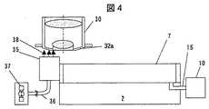
図3に液浸部分の図を示す。対物レンズ30の先端部とウェハ1は液槽7に供給された液5に浸されている。液槽7と液供給・排出機構10はパイプ15で配管されている。ウェハ1をチャック2にローディングする前は、液槽7は空である。ウェハ1をチャック2にローディング後、液槽7に液5を供給し、対物レンズ30とウェハ1を液で満たす。ローディング後、ウェハ1上の位置決めマークをイメージセンサ44などで撮像してその位置を画像処理部54で検出してメカニカルコントローラ58を介してステージを位置決めしてアライメントを行い、検査を開始する。ウェハ全面を検査するためには、ウェハ1を水平方向に走査させる必要がある。この走査するときに液体5の表面に波が生じ、対物レンズ30とウェハ1の間に泡が入り込む可能性がある。この泡が光学像として形成された場合、ウェハ1の欠陥ではないため、欠陥の誤検出となる。これを防止するため、対物レンズ30の先端部に整流板34を配置する。対物レンズ30の鏡筒の外径を40mmφ程度にした場合、整流板34の外径は60〜80mmφ程度となる。この整流板34により、ウェハ1と対物レンズ30間の液体5の流れをスムーズにし、泡の巻き込み等も抑制する。 FIG. 3 shows a liquid immersion portion. The tip of the
また、対物レンズ30の先端部32aは、表面改質しておくと良いケースがある。この目的は、レンズ表面への気泡の付着防止や液体5のスムーズな流れである。このため、レンズ表面やレンズ先端部32aのレンズホルダ部を予め表面改質しておく。例えば、レンズ先端部32aを予め酸化チタン膜をコーティングし、親水性処理を施しておく。この処理は、時間と共に特性が変化するため、液槽7の周辺にUV(Ultraviolet)光源37を配置しておき、発光したUV光を光ファイバ36でUV光照射部35に導く。ウェハ1がチャック2からアンローディングされている時に、図4で示すとおり、対物レンズの先端部32aにUV光38を照射し、光触媒効果により親水性を持続させるようにする。 In some cases, the
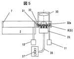
また、対物レンズ30の先端部32aに汚れなどが付着すると光学像の像質が低下する。この汚れ洗浄方法について、図5を用いて説明する。ウェハ1をアンローディングしている間は、対物レンズ1の先端部32aを、洗浄効果のある液体9(5)を供給した対物レンズ洗浄槽33に浸しておく。同時に、対物レンズ30の先端部32aをUV光照射部35で透明窓31を通してUV光照射することにより、親水性も改善する。この洗浄液9としては、アルコール系液体や純水及びフッ素系液体などが考えられる。また、洗浄液9を検査時に液浸する液体5と同じ液を用いることにより、液体供給排出機構や配管を共有化することが可能となり、装置の省スペース・低コスト化に有利である。尚、洗浄槽33の洗浄液9(5)は供給排出機構11により、液体の供給と排出を行う。 Further, if dirt or the like adheres to the
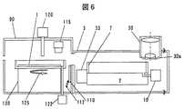
次に、液浸検査を行う前の準備処理の実施例について、図6を用いて説明する。ところで、欠陥検査の場合、図31に示すように、パターンの材質や構造に関する液浸方式において課題を有することになる。図31は、検査ウェハ1上に形成されたパターン1bを液体5で浸した例を示す。ウェハ1の表面に液体5を液浸して検査しようとしたとき、パターン1bの段差部に水が満たされず、気泡600が付着する可能性がある。このように気泡600が付着していると、対物レンズ30で拡大投影した光学像に気泡600の像が形成されることになる。しかしながら、この気泡600の像は、パターン1bの形状不良ではないため、パターン1bの欠陥として検出すべきではない。従って、液浸して検査する前の準備過程として気泡600を除く処理が必要となる。 Next, an example of the preparation process before the immersion inspection will be described with reference to FIG. By the way, in the case of defect inspection, as shown in FIG. 31, there is a problem in the liquid immersion method regarding the material and structure of the pattern. FIG. 31 shows an example in which the
また、欠陥検査では、図32に示すように、埋め込み前のコンタクトホール(スルーホール)を検査対象となる機会が多い。コンタクトホール1dが導通材を埋め込み前である場合、コンタクトホール1dは中空である。この表面に液体5を浸した場合、特定のコンタクトホール径以下の場合は、液体5がコンタクトホール1dに入り込まない。従って、液浸して検査するときには、コンタクトホール1dの形状や径が均一に形成されている場合は、コンタクトホールの表面層において液体5も同様な形状であることが望ましい。しかしながら、液浸して検査するとき、形状5dのように異なる形状になってしまった場合には、5dに示すコンタクトホール部が不均一な光学像として検出するため、虚報欠陥となる可能性がある。従って、液浸して検査する前の準備過程として、コンタクトホール1dの表面層において液体5の界面形状も同様な形状にしておく処理が必要となる。 In defect inspection, as shown in FIG. 32, there are many opportunities to inspect contact holes (through holes) before filling. When the
そこで、液浸して検査する前の準備過程として、検査準備室90に搬送されたウェハ1をノッチ検出用回転機構130に搭載し、この回転機構130を矢印125で示すように回転し、ノッチ検出器115でノッチを検出する。このあと、ノッチを所定の方位に粗位置合わせし、ウェハ1を検査ステーション3に搬入されてチャック2に搭載して液体5で浸して実際の検査が行われることになる。 Therefore, as a preparatory process prior to immersion and inspection, the
このように液浸して検査する前の準備過程において、気泡600を除く処理とコンタクトホール1dの表面層において液体5の界面形状も同様な形状にしておく処理とが必要となる。 Thus, in the preparatory process before immersion inspection, processing for removing the
図7には、全面液浸による検査ステーション3と検査準備室90とを備えた光学式外観検査装置の概略構成を示す。 FIG. 7 shows a schematic configuration of an optical appearance inspection apparatus provided with an
図7に示すとおり、検査準備室90でノッチを所定の方位に粗位置合わせした後、事前液浸機構120により液5aを供給することによってウェハ1上に浸す。単純に浸しただけでは、ウェハ1の表面に気泡が付着したままである恐れがあるため、事前に、回転機構130でウェハ1を回転させること(ウェハ液中スピン)によって気泡が除去されると共に、コンタクトホール1dが形成されている場合コンタクトホール1dの表面層において液体5の界面形状も均一な形状となる。尚、事前液浸機構120により供給する液5aは、全体になじませたいので、親水性の高いものでよく、検査時の液5と同一である必要はない(同一であっても良い)。また、液5aと検査時の液5が異なる場合、それぞれの蒸気が化学反応を起こすような場合は、準備室90と検査ステーション3を間仕切り110で開閉する機構112を設けておくと化学反応を防止できる。 As shown in FIG. 7, after the notch is roughly aligned in a predetermined orientation in the
また、他の気泡除去等の処理手段を図8に示す。ノッチを所定の方位に位置合わせ後、事前液浸機構120により液5aを供給してウェハ1上に浸す。次に振動発生装置140で駆動される超音波振動源141により液体を振動させ(ウェハ液中超音波振動)、ウェハ1に付着した気泡を除去すると共に、コンタクトホール1dが形成されている場合コンタクトホール1dの表面層において液体5の界面形状も均一な形状となる。 FIG. 8 shows another processing means such as bubble removal. After aligning the notch in a predetermined direction, the liquid 5 a is supplied by the
即ち、事前準備処理として、図26に示すように、Vノッチ合せによるプリアライメント(S263)、事前液浸(S264)、ウェハ界面の泡抜き(S265)および事前液浸液抜き(ウェハ表面の液切りはしない)(S266)を行う。ウェハ界面の泡抜きの方法としては、上述したように、ウェハ液中スピンの方法、ウェハ液中超音波振動の方法または減圧処理の方法を実行することになる。なお、検査準備室の圧力を減圧する減圧処理でも、ウェハ1に付着した気泡を除去すること(ウェハ界面の泡抜き)は可能である。 That is, as shown in FIG. 26, as pre-preparation processing, pre-alignment by V-notch alignment (S263), pre-immersion (S264), bubble removal from the wafer interface (S265), and pre-immersion liquid removal (wafer surface liquid (Do not cut) (S266). As described above, as a method for removing bubbles at the wafer interface, a method for spinning in the wafer liquid, a method for ultrasonic vibration in the wafer liquid, or a method for reducing the pressure is performed. In addition, it is possible to remove bubbles adhering to the wafer 1 (foam removal from the wafer interface) even by a decompression process in which the pressure in the inspection preparation chamber is reduced.
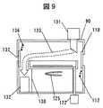
次に、液浸検査を実施した後のウェハ乾燥の実施例について、図9を用いて説明する。即ち、検査を終えたウェハ1は、準備室90に搬入されてウェハ1に付着した水分を乾燥させてカセット80に戻される(S274、S275)。準備室90におけるウェハ1の水分乾燥機能として、回転機構130によるスピン乾燥を行う。このとき、飛ばされた水分が霧となって乾燥後のウェハ1に再付着する恐れがある。この再付着を防止するため、送風機構131により気体を送り、吸気機構132により気体を排気する。これにより、霧をスムーズに検査準備室90から排出でき、ウェハ1への再付着を防ぐ。また、図10にエアナイフによる乾燥手段を示す。検査後、検査準備室90に搬送されたウェハ1は気体噴射器150でウェハ1の表面に気体を噴射し、ウェハ1表面の液体を吹き飛ばす。吹き飛ばされた液滴は吸気機構155に吸い込まれる構成である。これにより、吹き飛ばされた霧状の液滴も検査準備室90から排出することが可能となり、ウェハ1への再付着を防ぐことが可能となる。 Next, an example of wafer drying after the immersion inspection will be described with reference to FIG. In other words, the
尚、図9及び図10で送風・噴射する気体は、空気や窒素及びイソプロピルアルコールの蒸気などが考えられる。特に、イソプロピルアルコールの蒸気を用いた場合は、乾燥の効果が高くなることが期待できる。 9 and 10 may be air, nitrogen, isopropyl alcohol vapor, or the like. In particular, when isopropyl alcohol vapor is used, it can be expected that the drying effect is enhanced.
また、ウェハ乾燥の方法としては、減圧IPA(イソプロピルアルコール)のベーパー処理が考えられる。 As a method for drying the wafer, a vapor treatment with reduced pressure IPA (isopropyl alcohol) is conceivable.
次に、局所液浸による検査の実施の形態について図11〜図20を用いて説明する。 Next, an embodiment of inspection by local liquid immersion will be described with reference to FIGS.
液浸手法としては、図1で示したウェハ1の全面液浸手法と対物レンズ30とウェハ1の間のみを液浸する局所液浸手法がある。図11に局所液浸手法を示す。基本構成は、図1と同じである。異なる点は、検査ステーション3の内部のみである。例えば、イメージセンサ44がリニアイメージセンサタイプであった場合、ウェハ1を定速移動させながら画像を取得する。液体5は、液体供給排出機構10から特定の圧力(流量)で液体供給制御部181に送り込まれる。液体供給制御部181で流量や温度などを制御された液体は、ウェハ1が対物レンズ30を通過する手前の配管170をたどってウェハ1上に供給される。ウェハ1に供給された液体5は、ウェハ1の移動(ここでは、図面上、左から右に移動)方向に沿って対物レンズ30の下を流れ、対物レンズ30を通過した後、配管175aをたどって液体排出制御部179に導かれて排出される。液体排出制御部179に排出された液体は、液体供給排出機構10に流れ出る。これにより、ウェハ1が移動中であっても、ウェハ1と対物レンズ30の間は常に水で満たすことが可能となる。また、ウェハ1の移動方向が反対(ここでは、図面上、右から左に移動)方向になった場合は、配管170aで液体をウェハ1上に供給し、対物レンズの下を流れ、配管175で吸い取られる。従って、ウェハ1を移動させながら画像を取得する場合、対物レンズ30に対して手前で液体を供給し、対物レンズを通過後に液体を排出する機構とする。尚、液体の供給制御部181及び排出制御部179は、それぞれ特定の圧力で液体供給排出機構10に配管されている。この液体の供給及び排出方式について、図12を用いて説明する。液体供給制御部181からの液体5は、2つの配管170と170aに分岐されている。ウェハ1が矢印211の方向に定速移動しているとした場合、配管170の弁171が開放され、配管170aの弁171aが閉まっている。このため、ウェハ1への液体の供給は、配管170のみで行う。配管170を通してウェハ1上に供給された液体5は、対物レンズ30とウェハ1の間を通過後、弁176aが開放されている配管175aを通じて液体排出制御部179に導かれる。このとき、配管175側の弁176は閉まっている。また、ウェハ1が矢印211と逆方向に移動している場合は、供給側の弁171aが開放され弁171が閉まり、排出側の弁176が開放され弁176aが閉まる。この弁の開閉制御を行うことにより、ウェハ1の移動方向が反転しても、対物レンズ30とウェハ1の間を常に満たすことが可能となる。尚、液体供給制御部181は、液体供給量を調整するレギュレータ182と液体の酸素濃度調整器183及び液体の温度制御器184で構成されている。また、液体排出制御部179は、液体排出量を調整するレギュレータ177が搭載されている。酸素濃度調整器(減圧による泡抜きの機能も含まれる。)183は、1)液体5によるウェハ1の酸化を防止するため、2)供給する液体に含まれるマイクロバブルを除去するため等に必要であることが望ましい。また、液中の酸素濃度調整手段183としては、ヘンリーの法則を利用した方式などが考えられる。また、液体5は温度が変わると屈折率も変化する。対物レンズ30は液体の屈折率を特定の値として光学設計しているため、屈折率変動があると収差が大きくなる。このため、液体5の屈折率変動を抑えるために温度制御器184が必要となる。この温度制御手段184としては、ペルチェ効果(熱電冷却)を利用した方式などが考えられる。これら酸素濃度調整機能183と液体温度制御機能184は、図1で示したウェハ全面液浸方式においても備えておくことが望ましい。 As the liquid immersion method, there are a whole surface liquid immersion method of the
特に、局所液浸法によるウェハ端の検査を行う場合には、ウェハの厚み分の段差が生じるため、ウェハ端からチャック2の表面に液体5が流れ出てしまう。このため、対物レンズ30とウェハ1の間を液体5で満たせなくなる。そこで、ウェハ1の外周部にウェハ1の厚みと同等となる段差4を近接して設けることが必要となる。これにより、ウェハ1の外周部を検査する場合においても、ウェハ1の外周部と段差部4の間の間隙は少量であるため、対物レンズ30とウェハ1の間を液体5で満たすことが可能となる(図11に記載)。また、ウェハローディング後から検査する前までに、ウェハ1の外周部と段差部4の間隙を液体5で満たしておくことにより、対物レンズ30とウェハ1の間を液体5で満たすことが可能となる。 In particular, when the wafer edge inspection is performed by the local liquid immersion method, a step corresponding to the thickness of the wafer is generated, so that the liquid 5 flows out from the wafer edge to the surface of the
対物レンズ30について、ウェハ1と対向する面の外観を図13に示す。ガラス31は照明する光やパターンで反射・回折した光が透過するウィンドである。液体供給排出口185は、ウィンド31を中心として対称に配置されている。また、幅Yd,深さZdで形成された溝は、供給した液を満たしたい領域である。ウェハ1に最も近接するのは面188aであり、この面188aとウェハ1の間隔がWD(Working Distance)となる。液はできる限りウェハ1上には残したくないため、溝以外(例えば、ウェハ1の進行方向と直交する水平面内の方向)に液が溢れ出るのを低減したい。このため、液で満たしたい溝の部分32bは親水性、溝以外の面188aは撥水性の表面処理を行うことによりウェハ1上への液残り低減効果が期待できる。また、WD量の調整によっても液残りの低減を期待できる。望ましいWD量としては、0.7mm程度以下(より良くは0.3mm程度以下となる。)である。また、次の(4)式に供給する液と排出する液の関係式を示す。液で満たすZ寸法をZd+WD,液で満たすY寸法をYd,ステージ走査速度をVst,液供給量をVin,液排出量をVoutとした場合、液供給量Vinは液排出量Vout以上の量とすべきである。この関係式を(4)式に示す。 The appearance of the surface of the
Vin≧Vout=(Zd+WD)×Yd×Vst (4)
液体供給排出口185の形状の一例を図14に示す。(a)ではウィンド31を中心として対称的にそれぞれ1つの液体供給排出口185が形成されている。これに対して、(b)では液体供給排出口185がそれぞれ複数の穴で構成されている。これにより、溝の中心部と周辺部で水の供給及び排出量を比較的均等にすることが可能となる。Vin ≧ Vout = (Zd + WD) × Yd × Vst (4)
An example of the shape of the liquid supply /
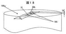
局所液浸方式として、液の供給排出口を対物レンズ30の鏡筒と分離した実施例を図15に示す。ウェハ1が矢印211の方向に走査する場合、液体供給制御部181の弁171が開放され、鏡筒から分離した位置191からウェハ1に対して液体5が連続して供給される。供給された液体5は表面張力によりウェハ1上に付着し、ウェハ1の移動に伴って対物レンズ30の溝の領域を満たすことになる。その後、対物レンズ30を通過した液体5は、液体排出制御部176aの弁が開放されることによって、鏡筒から分離した位置190から吸い上げられて液体5を排出する。ウェハ1の走査方向が逆転した場合の液体供給制御部181及び液体排出制御部179に配置されている弁171、171a、176、176aの開閉状態は、図12と同様である。また、図16に対物レンズ30のウェハ対向面の形状を示す。面188aがウェハ1に最も近接する面であり、面32bが液を満たしたい溝の部分である。ウィンド31付近では、溝の幅を狭くして液が満たされ易くし、空気層ができにくくする。 FIG. 15 shows an embodiment in which the liquid supply / discharge port is separated from the lens barrel of the
次に、図12で示した局所液浸方式の変形例を図17を用いて説明する。液体供給制御部181及び液体排出制御部179の動作及び弁171,171a,176,176aの開閉状態は、図12と同様である。液体5を満たす溝32bには、全周囲に壁188bが形成されている。図18には対物レンズ30のウェハ対向面の形状を示す。液体を満たす溝32bには、ステージ進行方向にも面188bの段差が設けられている。この溝の形状の一実施例を図19に示す。(a)ではウィンド31を中心として対称的にそれぞれ1つの液体供給排出口185が形成されている。これに対して、(b)では液体供給排出口185がそれぞれ複数の穴で構成されている。(c)ではウェハの2次元的な動きに対応させるため、ウェハ1に最も近接する段差面188bをリング状に形成する。このリングの内側に液体供給口185aが形成されており、液5を供給する。この内径部で液を供給すると、段差面188bから液が溢れ出る。この溢れ出た液体を段差面188bの外側に配置した複数の排出口185bで排出する。これにより、ウェハ1が面内で様々な方向に移動した場合でも段差面188bの内側で液体を満たし、外側で排出することが可能な形状となる。これは、検出した欠陥の観察を行うとき等にも有効である。即ち、欠陥の観察を行う場合、欠陥と欠陥との間を最短距離で移動したいため、欠陥の位置によって様々な方向に移動させる必要があるからである。 Next, a modification of the local liquid immersion method shown in FIG. 12 will be described with reference to FIG. The operations of the liquid
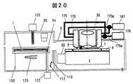
以上説明した局所液浸による検査の場合でも、全面液浸による検査の実施の形態で説明したように、ウェハに対する準備処理および検査後のウェハに対する乾燥処理は準備しておくことが望ましい。図20には、局所液浸による検査ステーション3と検査準備室90とを備えた光学式外観検査装置の概略構成を示す。 Even in the case of the inspection by the local liquid immersion described above, it is desirable to prepare the wafer preparation process and the wafer dry process after the inspection as described in the embodiment of the whole surface liquid immersion inspection. FIG. 20 shows a schematic configuration of an optical appearance inspection apparatus including the
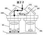
次に、光学式外観検査装置において、対物レンズの倍率を変更する実施例について図21を用いて説明する。即ち、検査装置では、対物レンズの倍率を変更ケースがある。例えば、高感度検査が必要なウェハでは高倍率検査,比較的低感度検査で問題ないウェハでは低倍率高スループット検査が効率的である。このため、要求される検査感度に応じて検査倍率を変更するケースがある。倍率を大幅に変更する場合は、対物レンズの交換が有効である。この複数の対物レンズを搭載する方法を図21に示す。レボルバ355に複数の対物レンズ30,30aが配置されている。これらの対物レンズは、少なくても1本は液浸用対物レンズである。レボルバ355は、モータ365に取り付けられた歯車360の回転によって、水平方向に回転350する。これによって、対物レンズを交換する。但し、対物レンズ30の先端に液体の供給排出口がある場合は、レボルバ355の回転時に液体供給排出機構と対物レンズの液配管を一時的に切り離し、レボルバ停止後に配管を接続する必要がある。このため、レボルバを利用する場合は、図15に示した対物レンズ30と液体供給・排出口を分離した構成が構成上シンプルである。また、液浸系対物レンズと乾燥系対物レンズを混載するケースも考えられる。この場合の実施例を図22に示す。液浸系対物レンズ30と乾燥系対物レンズ30bが1本ずつ搭載されているケースでは、対物レンズをそれぞれベース356に固定する。液浸系対物レンズ30で検査する場合は、照明光24を三角ミラー370によりミラー380の方に反射させ、液浸系対物レンズ30側に導く。また、乾燥系対物レンズ30bを用いて検査する場合は、三角ミラー370を三角ミラースライド機構375を移動させて、照明光をミラー381側に反射させる。これにより、乾燥系対物レンズ30b側に照明光を導き、乾燥系対物レンズ30bによる光学像を形成することが可能となる。これにより、三角ミラー370から対物レンズ30,30bまでの光路以外の光学系(照明系や検出系)は共通な光路となり、比較的シンプルな構成で液浸系と乾燥系の切換えが可能となる。液浸系対物レンズ30を乾燥系にも使える構成を図23に示す。(a)は液浸用に収差補正された対物レンズ30である。液浸による検査の場合は、対物レンズ30とウェハ1の間を液体で満たして検査する。この液浸系対物レンズ30を乾燥系で使う場合は、対物レンズ30とウェハ1の間を空気などの気体にする。この場合、液体と空気では屈折率が異なるため、収差が増大する。このため、光学像の解像度は極端に悪くなる。これを補正するための平行平板ガラス390と平行平板ガラススライド機構391を備えておく。(b)に示す通り、乾燥した状態で液浸系対物レンズ30を使う場合は、平行平板ガラス390を平行平板ガラススライド機構391で対物レンズ30とウェハ1の間に配置する。これにより、液浸系対物レンズ30を乾燥した状態で使用しても、収差を補正することが可能となる。これにより、液浸系対物レンズ30の2通りの使用が実現できる。尚、平行平板ガラス390は、ウェハ1とは接触しないギャップを設けて配置される。 Next, an embodiment in which the magnification of the objective lens is changed in the optical appearance inspection apparatus will be described with reference to FIG. That is, in the inspection apparatus, there is a case where the magnification of the objective lens is changed. For example, a high-magnification inspection is efficient for a wafer that requires a high-sensitivity inspection, and a low-magnification high-throughput inspection is efficient for a wafer that has no problem with a relatively low-sensitivity inspection. For this reason, there are cases where the inspection magnification is changed according to the required inspection sensitivity. When the magnification is changed greatly, it is effective to replace the objective lens. A method of mounting the plurality of objective lenses is shown in FIG. A plurality of
次に、液浸法による暗視野照明方式の実施例について図24及び図25を用いて説明する。図24は、全面液浸法を用いた暗視野照明方式の実施例を示す図である。暗視野照明方式として、ウェハ1を斜方照明(オフアクシス照明)400し、ウェハ1の異物やパターンで散乱・回折した光を対物レンズ30で捕捉し、暗視野像を形成する。照明光は液体表面の波による入射角の変動を抑えるため、液体5の中に浸した光学ウィンド405を通して照明する必要がある。また、対物レンズ30からイメージセンサ44までの構成は、図1と同じである。また、対物レンズ30の射出瞳位置或いは射出瞳と共役な位置に空間フィルタを配置し、特定の周波数帯をカットすることにより、周期的なパターンからの回折光をカットすることが可能となる。これにより、異物からの散乱光のみを検出することが可能となり、異物や凹凸欠陥の検査に有利となる。尚、図24では斜方照明系を1系統しか記載していないが、複数系統の斜方照明系を搭載し、複数方向からの照明を行うことも可能である。 Next, an embodiment of a dark field illumination method using an immersion method will be described with reference to FIGS. FIG. 24 is a diagram showing an example of a dark field illumination method using the whole surface immersion method. As the dark field illumination method, the
図25は、局所液浸法を用いた暗視野照明方式の実施例を示す図である。図25に示すように、対物レンズ30の外側に斜方照明光路410を設け、プリズム415に暗視野照明光を入射させる。このプリズム415の反射面417で対物レンズ30の視野を斜方照明する。ウェハ1の異物やパターンで散乱・回折した光を対物レンズ30で捕捉し、暗視野像を形成する。尚、図25では斜方照明系410、415を対物レンズ30を挟み込む2系統を記載しているが、暗視野照明系をさらに増やすことも容易に考えられる。極端な例では、リング状のプリズムを用いることにより、対物レンズ30の光軸を中心とした全方位の暗視野照明を行うことが可能となる。 FIG. 25 is a diagram illustrating an example of a dark field illumination method using a local liquid immersion method. As shown in FIG. 25, an oblique
以上、液浸法による暗視野照明方式の構成を説明したが、乾燥系の暗視野照明に比べて有利な点は、1)解像度の向上、2)薄膜干渉の抑制による散乱光検出強度の安定化がある。これにより、暗視野照明方式においても、高感度検査が可能となる。 In the above, the configuration of the dark field illumination method by the immersion method has been described. However, the advantages of the dark field illumination of the dry system are as follows: 1) Improvement of resolution, 2) Stable detection of scattered light intensity by suppressing thin film interference There is. As a result, high-sensitivity inspection is possible even in the dark field illumination system.
また、図24及び図25で示した暗視野照明方式と、図1や図11で示した明視野照明方式の混載する構成も考えられる。混載した場合は、明暗視野複合照明や明視野単独照明及び暗視野単独照明が可能となり、様々な欠陥への欠陥検出対応力が強化できる。 A configuration in which the dark field illumination method shown in FIGS. 24 and 25 and the bright field illumination method shown in FIGS. 1 and 11 are mixedly mounted is also conceivable. In the case of mixed mounting, bright / dark field composite illumination, bright field single illumination and dark field single illumination are possible, and the ability to detect defects to various defects can be enhanced.
これまでに説明した実施例についての、検査フローの一実施例を図26に示す。まず、カセット80内に検査着工待ちのウェハが格納されている。搬送系85でウェハを検査準備室90に搬送する(S262)。搬送されたウェハ1は、ウェハのVノッチ(或いはオリエンテーションフラット)を検出し、ウェハのθ方向の粗位置合わせを行う(S263)。次に、事前液浸を行い(S264)、ウェハと液の界面の泡抜きを行う(S265)。泡抜きの手法としては、1)ウェハの液中スピン、2)ウェハ液中超音波振動、3)減圧処理、などがある。泡抜き処理を終えたあとは、事前液浸の液抜きを行う(S266)。このとき、乾燥処理は行わないため、ウェハパターンの微小な段差に入り込んだ液は、付着したままとなる。次にウェハを検査ステーション3にローディングする(S267)。検査ステーションのチャックに配置されたウェハは、検査用の液浸を行う(S269)。この液浸方法としては、上述したように、1)ウェハ全面液浸、2)局所液浸、がある。尚、液浸用の供給液は、温調(手段の例:ペルチェ効果による熱電冷却など),泡抜き(手段の例:減圧処理など),酸素濃度制御(手段の例:低酸素濃度雰囲気処理など)等の処理を行っている(S268)。これらの液体で液浸した後にウェハ走査と画像検出を行い、画像処理部で画像比較による欠陥検査を行う(S270)。検査終了後は、検査用液浸の液抜きを行い(S271)、ウェハを検査準備室90にアンローディングする(S272)。アンローディングされたウェハは、ウェハの乾燥を行う(S274)。乾燥処理としては、1)減圧IPA(イソプロピルアルコール)ベーパー処理、2)ウェハスピン、3)気体噴射、などが考えられる。乾燥したウェハは、搬送系によりカセットに格納される(S275)。以上が検査シーケンスである。尚、非検査中は、対物レンズの液浸エリアを活性化させるため(S273)、ウェハ対向面にUVを照射させることも考えられる。以上、簡単な検査シーケンスを説明したが、シーケンス順の変更や不要な処理を省くことは容易に推測できることであり、本発明に含まれる内容である。 FIG. 26 shows an embodiment of the inspection flow for the embodiments described so far. First, a wafer waiting for inspection start is stored in the
次に、半導体ウェハパターンの形成プロセスの実施例について図27を用いて説明する。図27(a)に半導体ウェハパターンの形成プロセスを示す。まず、ウェハ1にパターンの材料を成膜し、レジストを塗布する。次にパターンを露光し、現像及びエッチングする。次にレジストを除去して洗浄し、欠陥検査を行う。これらのパターンの上にパターンを積層する場合は、また成膜処理されるというループになる。このうち、洗浄と欠陥検査処理のフローを図27(b)に示す。洗浄工程では、薬液洗浄され純水洗浄する。この薬液洗浄と純水洗浄は、洗浄対象物に応じて複数回行われることがある。この後、乾燥処理が施され、欠陥検査工程に進む。検査工程では、光学式外観検査装置を用いてウェハを液浸して欠陥検査する。この後、ウェハを乾燥させる。ここで、洗浄から欠陥検査の間に2回の乾燥処理が施される。これを1回にするショートカットプロセスを図27(c)に示す。例えば、洗浄と欠陥検査は、1つの装置で実施される。この場合、薬液洗浄,水洗浄の後に液浸処理を行い、欠陥検査の後に乾燥処理を行う。この場合、乾燥処理は、検査後の1回のみであり、製造プロセスの簡素化に有効である。この簡易プロセスを実現する形態を図28に示す。レジスト除去が終了してカセット80に格納されているウェハは、搬送系85で洗浄室325に搬入される。洗浄室では、洗浄対象に応じた複数の液槽330a,b,c(水洗槽も含む)があり、洗浄と水洗が行われる。尚、洗浄液はタンク335aより供給される。最後の水洗の後、ウェハは光学系が配置されている検査ステーションに搬入され、ノッチ検出部でθ方向の粗位置合わせが行われる。次に、ウェハチャック2にウェハを搭載し、液浸法による欠陥検査を行う。検査終了後はウェハを洗浄室に搬入し、必要に応じてウェハを水洗する。次に、このウェハは乾燥室300に搬入され、例えば減圧・過熱IPAベーパー処理が行われる。加熱プレート320で乾燥チャンバ305内を所定の温度に調節し、IPA315の蒸気をチャンバ305内に送り込み、真空ポンプ310で減圧する。これにより、ウェハパターンに付着した水分を乾燥させることが可能である。この乾燥処理後に、ウェハをカセット80に格納する。 Next, an example of a semiconductor wafer pattern forming process will be described with reference to FIG. FIG. 27A shows a process for forming a semiconductor wafer pattern. First, a pattern material is formed on the
次に、液浸法を用いた外観検査用光学系の構成例を図29を用いて、光学系の解像度向上手段を以下に説明する。
(1)対物レンズ30とウェハ1の間隔を液体5で浸して、解像度を向上する。
(2)落射照明・明視野検出方式において、ケーラー照明方式を適用している場合、光源22の像を開口絞り425に結像する。この開口絞り425の像を対物レンズ30の瞳に結像させる。この開口絞り425の開口部を輪帯状(リング状)にすることにより、ウェハ1の一点を照明する光は、垂直照明成分がない斜方照明となる。この照明により、空間周波数の高周波側MTF(Modulation Transfer Function)が向上する。
(3)更に、ビームスプリッタ40aを偏光ビームスプリッタタイプとすることにより、ビームスプリッタ40aを反射した光は、直線偏光となる。この直線偏光が波長板430を透過して楕円偏光となって、ウェハ1を落射照明する。照明した偏光光は、ウェハ1のパターンで反射・回折・散乱するときに偏光状態に変調を受ける。これらの光が再び波長板430を透過し、偏光ビームスプリッタ40aに入射する。この偏光ビームスプリッタ40aを透過したP偏光がウェハ1の光学像を形成し、イメージセンサ44で検出される。このように、偏光ビームスプリッタ40aは検光子の役目を果たすことになる。従って、ウェハ1のパターンで反射・回折・散乱するときの偏光状態に応じて照明光の偏光状態を調整しておき、偏光ビームスプリッタ40aを透過する正反射光・高次回折光・散乱光で形成される光学像が欠陥検出上有利な像となるように調整する。欠陥検出上有利な像とは、欠陥部のコントラストを向上できる像を指す。
(4)上記(2)で説明した輪帯状の開口絞り425を用いてウェハ1を照明した場合、対物レンズ30の瞳位置では、0次光(正反射光)と高次回折光が分離している。このため、この瞳位置に0次光と高次回折光(1次以上)のそれぞれについて透過率や相対的な位相差を調整する空間フィルタ420を配置することにより、ウェハ1のパターンを強調して検出することが可能である。これは、位相差顕微鏡の原理による。尚、対物レンズ30の瞳位置は、対物レンズ30の内部に形成されることが多く、空間フィルタを配置するスペースがない。このため、対物レンズ30の瞳と共役な位置を設け、この共役位置に空間フィルタ420を配置する。これにより、光学像の高解像度化や欠陥検出に有利な像を形成することが可能となる。Next, a configuration example of an optical system for appearance inspection using the liquid immersion method will be described below with reference to FIG.
(1) The interval between the
(2) In the epi-illumination / bright field detection method, when the Kohler illumination method is applied, an image of the
(3) Furthermore, by making the
(4) When the
以上、(1)に液浸法、(2)〜(4)に解像度向上技術を記載した。これらの組合せにより、さらに光学系の高解像度化を実現することが可能となり、高感度検査に有効となる。 As described above, the immersion method is described in (1), and the resolution improvement technique is described in (2) to (4). By combining these, it becomes possible to realize higher resolution of the optical system, which is effective for high-sensitivity inspection.
次に、図1、図11で示した画像処理部54の具体的実施例について説明する。イメージセンサ44(ここでは、リニアイメージセンサとする)で検出されたウェハ1の画像は、A/D変換器50でデジタル画像として画像処理部54に入力される。入力された画像は、位置ずれ検出部510と遅延メモリ500に分岐される。遅延メモリ500は、ダイ比較の場合は隣接したダイに対応した時間(あるいは、セル比較の場合は隣接したセルに対応した時間)分を遅延させた画像を、位置ずれ検出部510に入力する。このため、位置ずれ検出部510に入力される画像は、ウェハ1に形成された設計上同一パターンである隣接ダイ(あるいは、セル)の画像である。この2画像の位置ずれ量を位置ずれ検出部510で検出した後、このずれを位置合わせ部520で位置合わせする。この位置合わせ部520における位置合わせは、サブ画素単位で実施する。この位置合わせした画像の差画像を差画像演算部530で実施する。この差画像の特徴量に基づいて、欠陥判定部540で欠陥候補550を判定する。この欠陥判定部540にて欠陥として判定する特徴量としては、濃淡差,濃淡差しきい値以上となるサイズ,検出画像の明るさ,画像のコントラスト,欠陥座標情報などがある。この欠陥判定部540で検出された欠陥候補550は、欠陥の座標情報を欠陥分類部570に入力される。位置合わせ部520から分岐された隣接ダイの画像は、画像メモリ560に一時格納されており、欠陥分類部570に入力された欠陥候補の座標に対応した画像を読み出すことが可能である。欠陥分類部570では、読み出した隣接ダイの画像を用いて、欠陥の分類を行う。この分類結果と欠陥候補550の情報をデータサーバ62に格納する。尚、欠陥分類部570は、異物やパターン欠陥及び欠陥によるデバイスへの致命性などが判断される。従って、データサーバ62に格納される情報は、欠陥候補550の座標情報や大きさ及び分類結果が格納され、さまざまな欠陥情報を有機的に欠陥観察工程へ送られる。 Next, a specific example of the
以上、液浸法による欠陥検査手段及び液浸検査シーケンスなどを説明したが、それぞれの実施例の組合せや複合及び検査シーケンス順の変更や省略などは容易に考案できるものであり、それらの内容は本発明に含まれるものである。 As described above, the defect inspection means and the immersion inspection sequence by the immersion method have been described, but the combination and combination of each embodiment and the change or omission of the inspection sequence order can be easily devised, and their contents are as follows. It is included in the present invention.
1…ウェハ(被検査対象物:試料)、2…チャック、3…検査ステーション、4…段差部、5…液体、7…液槽、10…液体供給排出機構、22…光源、24…照明光、30…対物レンズ、31…ウィンド、32a…対物レンズの先端部分、32b…溝、34…整流板、35…UV照射部、37…UV光源、40…ビームスプリッタ、43…焦点検出用センサ、44…イメージセンサ、46…検出光、50…AD変換器、54…画像処理部、58…メカニカルコントローラ部、60…オペレーティングコントローラ、62…データサーバ、90…準備室、115…ノッチ検出器、120…事前液浸機構、130…回転機構、131…送風機構、132…吸気機構、141…超音波振動源、170…液体供給用配管、175…液体排出用配管、171…液体供給用弁、176…液体排出用弁、179…液体排出制御部、181…液体供給制御部、185…液体供給排出口、188a…面、188b…壁(段差)、300…乾燥室、310…ポンプ、315…イソプロピルアルコール、320…加熱プレート、325…洗浄室、330…洗浄液槽、335…タンク、370…三角ミラー、390…平行平板ガラス、391…ガラススライド機構、400…オフアクシス照明光、405…光学ウィンド、415…プリズム。 DESCRIPTION OF
Claims (21)
Translated fromJapanese前記光学像形成ステップにおいて、前記検出光学系を介して前記試料を照明し、前記試料からの反射光を用いて前記検出光学系の焦点と前記試料の位置関係とを示す焦点検出情報を得る焦点検出ステップを含むことを特徴とする欠陥検査方法。An optical image forming step of forming an optical image of the sample with the detection optical system in a state where the space between the sample and the tip of the detection optical system is immersed, and the optical of the sample formed in the optical image forming step A defect inspection step including a signal acquisition step of acquiring an image as an image signal by an image sensor, and a defect detection step of detecting a defect on the sample based on the image signal acquired in the signal acquisition step;
In the optical image formation step, the focus is obtained by illuminating the sample through the detection optical system and using the reflected light from the sample to obtain focus detection information indicating the focus of the detection optical system and the positional relationship of the sample A defect inspection method comprising a detection step.
Priority Applications (2)
| Application Number | Priority Date | Filing Date | Title |
|---|---|---|---|
| JP2003313897AJP2005083800A (en) | 2003-09-05 | 2003-09-05 | Defect inspection method and defect inspection apparatus |
| US10/893,988US7599545B2 (en) | 2003-09-05 | 2004-07-20 | Method and its apparatus for inspecting defects |
Applications Claiming Priority (1)
| Application Number | Priority Date | Filing Date | Title |
|---|---|---|---|
| JP2003313897AJP2005083800A (en) | 2003-09-05 | 2003-09-05 | Defect inspection method and defect inspection apparatus |
Publications (1)
| Publication Number | Publication Date |
|---|---|
| JP2005083800Atrue JP2005083800A (en) | 2005-03-31 |
Family
ID=34225149
Family Applications (1)
| Application Number | Title | Priority Date | Filing Date |
|---|---|---|---|
| JP2003313897APendingJP2005083800A (en) | 2003-09-05 | 2003-09-05 | Defect inspection method and defect inspection apparatus |
Country Status (2)
| Country | Link |
|---|---|
| US (1) | US7599545B2 (en) |
| JP (1) | JP2005083800A (en) |
Cited By (19)
| Publication number | Priority date | Publication date | Assignee | Title |
|---|---|---|---|---|
| JP2005234458A (en)* | 2004-02-23 | 2005-09-02 | Nikon Corp | Microscope observation device |
| WO2006093208A1 (en)* | 2005-02-28 | 2006-09-08 | Nikon Corporation | Microscope-use adaptor and microscope device |
| JP2006337073A (en)* | 2005-05-31 | 2006-12-14 | Advantest Corp | Testing apparatus and device manufacturing method |
| JP2009264739A (en)* | 2008-04-21 | 2009-11-12 | Nec Corp | Optical appearance inspection device and optical appearance inspection method |
| JP2009539109A (en)* | 2006-06-01 | 2009-11-12 | ケーエルエー−テンカー テクノロジィース コーポレイション | Order-selected overlay measurement |
| JP2010078400A (en)* | 2008-09-25 | 2010-04-08 | Toshiba Corp | Template inspecting method and defect inspection device |
| US7796343B2 (en) | 2007-12-26 | 2010-09-14 | Lasertec Corporation | Photomask inspection apparatus |
| US7868996B2 (en) | 2005-10-21 | 2011-01-11 | Nikon Corporation | Liquid immersion microscope |
| JP2013231741A (en)* | 2007-02-26 | 2013-11-14 | Corning Inc | Distortion measurement imaging system |
| KR20150013892A (en)* | 2012-09-28 | 2015-02-05 | 가부시키가이샤 히다치 하이테크놀로지즈 | Defect inspection device and defect inspection method |
| US9128064B2 (en) | 2012-05-29 | 2015-09-08 | Kla-Tencor Corporation | Super resolution inspection system |
| JP2015200610A (en)* | 2014-04-10 | 2015-11-12 | 株式会社レイテックス | Defect measurement device and defect measurement method |
| JP2017146294A (en)* | 2016-02-12 | 2017-08-24 | 国立研究開発法人産業技術総合研究所 | Indenter transmission type specimen surface observation device and observation method, moving image analysis program, device control program, and characteristic value calculation program |
| JP2018077148A (en)* | 2016-11-10 | 2018-05-17 | 株式会社ディスコ | Inspection method |
| JP2020173141A (en)* | 2019-04-09 | 2020-10-22 | 株式会社ミツトヨ | Surface shape measuring system and surface shape measuring method using surface shape measuring instrument |
| CN113299547A (en)* | 2020-02-21 | 2021-08-24 | 株式会社迪思科 | Method for processing wafer |
| CN113299546A (en)* | 2020-02-21 | 2021-08-24 | 株式会社迪思科 | Method for processing wafer |
| CN113299545A (en)* | 2020-02-21 | 2021-08-24 | 株式会社迪思科 | Method for processing wafer |
| JP2023531253A (en)* | 2020-06-29 | 2023-07-21 | 深▲セン▼華大智造科技股▲ふん▼有限公司 | Systems and methods for optical scanning and imaging through fluid media for nucleic acid sequencing |
Families Citing this family (34)
| Publication number | Priority date | Publication date | Assignee | Title |
|---|---|---|---|---|
| DE10343876B4 (en)* | 2003-09-23 | 2011-01-13 | Vistec Semiconductor Systems Gmbh | Device for measuring feature widths on masks for the semiconductor industry |
| JP4192118B2 (en)* | 2004-05-31 | 2008-12-03 | 株式会社日立ハイテクノロジーズ | Defect inspection apparatus and defect inspection system |
| WO2005124833A1 (en)* | 2004-06-21 | 2005-12-29 | Nikon Corporation | Exposure device, exposure device member cleaning method, exposure device maintenance method, maintenance device, and device manufacturing method |
| US8698998B2 (en)* | 2004-06-21 | 2014-04-15 | Nikon Corporation | Exposure apparatus, method for cleaning member thereof, maintenance method for exposure apparatus, maintenance device, and method for producing device |
| JP3870207B2 (en)* | 2004-08-05 | 2007-01-17 | キヤノン株式会社 | Immersion exposure apparatus and device manufacturing method |
| US20060055927A1 (en)* | 2004-09-16 | 2006-03-16 | Rosemount Analytical Inc. | Turbidity sensor |
| JP4708876B2 (en)* | 2005-06-21 | 2011-06-22 | キヤノン株式会社 | Immersion exposure equipment |
| JP4413831B2 (en)* | 2005-08-11 | 2010-02-10 | 株式会社日立ハイテクノロジーズ | Wafer surface inspection apparatus and wafer surface inspection method |
| IL181484A0 (en)* | 2007-02-21 | 2007-07-04 | Haim Shlezinger | A method for evaluation of a gemstone |
| DE102006011904B4 (en)* | 2006-03-09 | 2017-09-21 | Nagel Maschinen- Und Werkzeugfabrik Gmbh | Measuring method, measuring system and processing machine with measuring system |
| US8045134B2 (en) | 2006-03-13 | 2011-10-25 | Asml Netherlands B.V. | Lithographic apparatus, control system and device manufacturing method |
| JP4877075B2 (en)* | 2007-05-29 | 2012-02-15 | 東京エレクトロン株式会社 | Coating, developing device, coating, developing device operating method, and storage medium |
| US9151943B2 (en) | 2008-08-04 | 2015-10-06 | Fluid Imaging Technologies, Inc. | System and method for monitoring birefringent particles in a fluid |
| US8345239B1 (en)* | 2008-08-04 | 2013-01-01 | Fluid Imaging Technologies, Inc. | System and method for monitoring birefringent particles in a fluid |
| US20110143287A1 (en)* | 2009-09-14 | 2011-06-16 | Nikon Corporation | Catadioptric system, aberration measuring apparatus, method of adjusting optical system, exposure apparatus, and device manufacturing method |
| JP2012164812A (en)* | 2011-02-07 | 2012-08-30 | Toshiba Corp | System and method of manufacturing semiconductor device |
| US8994945B2 (en) | 2011-10-27 | 2015-03-31 | Fluid Imaging Technologies, Inc. | Method of treatment analysis with particle imaging |
| US8879073B2 (en)* | 2012-02-24 | 2014-11-04 | Kla-Tencor Corporation | Optical metrology using targets with field enhancement elements |
| KR101376831B1 (en)* | 2012-03-27 | 2014-03-20 | 삼성전기주식회사 | Surface defect detecting apparatus and control method thereof |
| US9164388B2 (en) | 2012-04-10 | 2015-10-20 | Kla-Tencor Corporation | Temperature control in EUV reticle inspection tool |
| US8879797B2 (en) | 2012-05-25 | 2014-11-04 | Fluid Imaging Technologies, Inc. | System and method for total internal reflection enhanced imaging flow cytometry |
| JP6228751B2 (en)* | 2013-04-26 | 2017-11-08 | 株式会社ニューフレアテクノロジー | Inspection device |
| US9885671B2 (en) | 2014-06-09 | 2018-02-06 | Kla-Tencor Corporation | Miniaturized imaging apparatus for wafer edge |
| US9645097B2 (en) | 2014-06-20 | 2017-05-09 | Kla-Tencor Corporation | In-line wafer edge inspection, wafer pre-alignment, and wafer cleaning |
| US10375901B2 (en) | 2014-12-09 | 2019-08-13 | Mtd Products Inc | Blower/vacuum |
| US9983115B2 (en) | 2015-09-21 | 2018-05-29 | Fluid Imaging Technologies, Inc. | System and method for monitoring particles in a fluid using ratiometric cytometry |
| JP7134096B2 (en)* | 2016-06-02 | 2022-09-09 | 東京エレクトロン株式会社 | Substrate inspection method, device and system |
| CN108387587B (en)* | 2018-01-22 | 2020-07-31 | 京东方科技集团股份有限公司 | Defect detection method and defect detection equipment |
| IL310215A (en)* | 2018-06-13 | 2024-03-01 | Asml Netherlands Bv | Metrology apparatus |
| US11544838B2 (en)* | 2020-03-21 | 2023-01-03 | Kla Corporation | Systems and methods of high-resolution review for semiconductor inspection in backend and wafer level packaging |
| CN112466787B (en)* | 2020-11-25 | 2025-03-14 | 上海果纳半导体技术有限公司 | Wafer defect inspection equipment |
| CN113720815B (en)* | 2021-07-21 | 2024-07-12 | 中国工程物理研究院激光聚变研究中心 | Fused quartz subsurface defect high-resolution imaging method under weak fluorescence imaging condition |
| US11761905B2 (en)* | 2021-08-26 | 2023-09-19 | Taiwan Semiconductor Manufacturing Company Limited | Inspection layer to improve the detection of defects through optical systems and methods of inspecting semiconductor device for defects |
| TW202505656A (en)* | 2023-07-20 | 2025-02-01 | 亞亞科技股份有限公司 | Detection equipment for defects after wafer dicing or arrangement |
Family Cites Families (18)
| Publication number | Priority date | Publication date | Assignee | Title |
|---|---|---|---|---|
| US4509852A (en)* | 1980-10-06 | 1985-04-09 | Werner Tabarelli | Apparatus for the photolithographic manufacture of integrated circuit elements |
| JPH05340885A (en)* | 1992-06-08 | 1993-12-24 | Matsushita Electric Ind Co Ltd | Particle inspection method |
| JPH06124873A (en) | 1992-10-09 | 1994-05-06 | Canon Inc | Immersion projection exposure system |
| JP2753930B2 (en)* | 1992-11-27 | 1998-05-20 | キヤノン株式会社 | Immersion type projection exposure equipment |
| US5825043A (en) | 1996-10-07 | 1998-10-20 | Nikon Precision Inc. | Focusing and tilting adjustment system for lithography aligner, manufacturing apparatus or inspection apparatus |
| US5900354A (en)* | 1997-07-03 | 1999-05-04 | Batchelder; John Samuel | Method for optical inspection and lithography |
| JPH1163944A (en) | 1997-08-15 | 1999-03-05 | Toshiba Corp | Surface pattern inspection method and inspection device |
| JPH11118728A (en)* | 1997-10-17 | 1999-04-30 | Kazama Engineering Kk | Work appearance inspection method and device |
| WO1999049504A1 (en) | 1998-03-26 | 1999-09-30 | Nikon Corporation | Projection exposure method and system |
| JP3610837B2 (en) | 1998-09-18 | 2005-01-19 | 株式会社日立製作所 | Sample surface observation method and apparatus, defect inspection method and apparatus |
| JP2001356278A (en) | 2000-06-13 | 2001-12-26 | Olympus Optical Co Ltd | Microscope system |
| US6630996B2 (en)* | 2000-11-15 | 2003-10-07 | Real Time Metrology, Inc. | Optical method and apparatus for inspecting large area planar objects |
| JP4059644B2 (en) | 2001-05-23 | 2008-03-12 | オリンパス株式会社 | Observation optical system |
| US6788477B2 (en)* | 2002-10-22 | 2004-09-07 | Taiwan Semiconductor Manufacturing Co., Ltd. | Apparatus for method for immersion lithography |
| US6781670B2 (en)* | 2002-12-30 | 2004-08-24 | Intel Corporation | Immersion lithography |
| US7130037B1 (en)* | 2003-01-09 | 2006-10-31 | Kla-Tencor Technologies Corp. | Systems for inspecting wafers and reticles with increased resolution |
| US6867844B2 (en)* | 2003-06-19 | 2005-03-15 | Asml Holding N.V. | Immersion photolithography system and method using microchannel nozzles |
| JP4192118B2 (en)* | 2004-05-31 | 2008-12-03 | 株式会社日立ハイテクノロジーズ | Defect inspection apparatus and defect inspection system |
- 2003
- 2003-09-05JPJP2003313897Apatent/JP2005083800A/enactivePending
- 2004
- 2004-07-20USUS10/893,988patent/US7599545B2/ennot_activeExpired - Fee Related
Cited By (34)
| Publication number | Priority date | Publication date | Assignee | Title |
|---|---|---|---|---|
| JP2005234458A (en)* | 2004-02-23 | 2005-09-02 | Nikon Corp | Microscope observation device |
| WO2006093208A1 (en)* | 2005-02-28 | 2006-09-08 | Nikon Corporation | Microscope-use adaptor and microscope device |
| JPWO2006093208A1 (en)* | 2005-02-28 | 2008-08-07 | 株式会社ニコン | Microscope adapter and microscope apparatus |
| JP2006337073A (en)* | 2005-05-31 | 2006-12-14 | Advantest Corp | Testing apparatus and device manufacturing method |
| US7868996B2 (en) | 2005-10-21 | 2011-01-11 | Nikon Corporation | Liquid immersion microscope |
| JP2009539109A (en)* | 2006-06-01 | 2009-11-12 | ケーエルエー−テンカー テクノロジィース コーポレイション | Order-selected overlay measurement |
| JP2014160874A (en)* | 2006-06-01 | 2014-09-04 | Kla-Encor Corp | Order selected overlay metrology |
| JP2013231741A (en)* | 2007-02-26 | 2013-11-14 | Corning Inc | Distortion measurement imaging system |
| US7796343B2 (en) | 2007-12-26 | 2010-09-14 | Lasertec Corporation | Photomask inspection apparatus |
| JP2009264739A (en)* | 2008-04-21 | 2009-11-12 | Nec Corp | Optical appearance inspection device and optical appearance inspection method |
| US8227267B2 (en) | 2008-09-25 | 2012-07-24 | Kabushiki Kaisha Toshiba | Template inspection method and manufacturing method for semiconductor device |
| JP2010078400A (en)* | 2008-09-25 | 2010-04-08 | Toshiba Corp | Template inspecting method and defect inspection device |
| US9128064B2 (en) | 2012-05-29 | 2015-09-08 | Kla-Tencor Corporation | Super resolution inspection system |
| KR20150013892A (en)* | 2012-09-28 | 2015-02-05 | 가부시키가이샤 히다치 하이테크놀로지즈 | Defect inspection device and defect inspection method |
| KR101895255B1 (en) | 2012-09-28 | 2018-09-05 | 가부시키가이샤 히다치 하이테크놀로지즈 | Defect inspection device and defect inspection method |
| JP2015200610A (en)* | 2014-04-10 | 2015-11-12 | 株式会社レイテックス | Defect measurement device and defect measurement method |
| JP2017146294A (en)* | 2016-02-12 | 2017-08-24 | 国立研究開発法人産業技術総合研究所 | Indenter transmission type specimen surface observation device and observation method, moving image analysis program, device control program, and characteristic value calculation program |
| JP2018077148A (en)* | 2016-11-10 | 2018-05-17 | 株式会社ディスコ | Inspection method |
| JP2020173141A (en)* | 2019-04-09 | 2020-10-22 | 株式会社ミツトヨ | Surface shape measuring system and surface shape measuring method using surface shape measuring instrument |
| JP7254422B2 (en) | 2019-04-09 | 2023-04-10 | 株式会社ミツトヨ | SURFACE PROFILE MEASURING METHOD USING SURFACE PROFILE MEASURING SYSTEM AND SURFACE PROFILE MEASUREMENT |
| KR20210106891A (en)* | 2020-02-21 | 2021-08-31 | 가부시기가이샤 디스코 | Wafer processing method |
| KR102814933B1 (en)* | 2020-02-21 | 2025-05-29 | 가부시기가이샤 디스코 | Wafer processing method |
| CN113299546A (en)* | 2020-02-21 | 2021-08-24 | 株式会社迪思科 | Method for processing wafer |
| KR20210106890A (en)* | 2020-02-21 | 2021-08-31 | 가부시기가이샤 디스코 | Wafer processing method |
| JP2021136247A (en)* | 2020-02-21 | 2021-09-13 | 株式会社ディスコ | Wafer processing method |
| JP2021136246A (en)* | 2020-02-21 | 2021-09-13 | 株式会社ディスコ | Wafer processing method |
| CN113299547A (en)* | 2020-02-21 | 2021-08-24 | 株式会社迪思科 | Method for processing wafer |
| CN113299545A (en)* | 2020-02-21 | 2021-08-24 | 株式会社迪思科 | Method for processing wafer |
| JP7446673B2 (en) | 2020-02-21 | 2024-03-11 | 株式会社ディスコ | Wafer processing method |
| JP7446672B2 (en) | 2020-02-21 | 2024-03-11 | 株式会社ディスコ | Wafer processing method |
| KR102864216B1 (en)* | 2020-02-21 | 2025-09-24 | 가부시기가이샤 디스코 | Method for processing wafer |
| KR102799914B1 (en)* | 2020-02-21 | 2025-04-23 | 가부시기가이샤 디스코 | Wafer processing method |
| JP2023531253A (en)* | 2020-06-29 | 2023-07-21 | 深▲セン▼華大智造科技股▲ふん▼有限公司 | Systems and methods for optical scanning and imaging through fluid media for nucleic acid sequencing |
| JP7639029B2 (en) | 2020-06-29 | 2025-03-04 | 深▲セン▼華大智造科技股▲ふん▼有限公司 | Systems and methods for optical scanning and imaging through fluid media for nucleic acid sequencing - Patents.com |
Also Published As
| Publication number | Publication date |
|---|---|
| US20050052642A1 (en) | 2005-03-10 |
| US7599545B2 (en) | 2009-10-06 |
Similar Documents
| Publication | Publication Date | Title |
|---|---|---|
| JP2005083800A (en) | Defect inspection method and defect inspection apparatus | |
| JP4192118B2 (en) | Defect inspection apparatus and defect inspection system | |
| US10267745B2 (en) | Defect detection method and defect detection device and defect observation device provided with same | |
| US6563586B1 (en) | Wafer metrology apparatus and method | |
| US9436990B2 (en) | Defect observation method and device therefor | |
| US6842298B1 (en) | Broad band DUV, VUV long-working distance catadioptric imaging system | |
| KR100995450B1 (en) | Optical device inspection mechanism and inspection method considering contamination | |
| JP5529729B2 (en) | Catadioptric microscope objective lens with immersion liquid for use in broadband microscopy | |
| US7359044B2 (en) | Method and apparatus for inspecting pattern defects | |
| US7268343B2 (en) | Method and system for detecting defects | |
| US20040095573A1 (en) | Excimer laser inspection system | |
| KR102630492B1 (en) | Method and system for characterizing optical surface defect materials | |
| KR20100007968A (en) | Surface tester and surface testing method | |
| JP2016008941A (en) | Defect observation method and apparatus, and defect detection apparatus | |
| US7130037B1 (en) | Systems for inspecting wafers and reticles with increased resolution | |
| US7796343B2 (en) | Photomask inspection apparatus | |
| US7868996B2 (en) | Liquid immersion microscope | |
| JP5571969B2 (en) | Defect inspection method and apparatus | |
| JP2009283987A (en) | Sensor shield | |
| US7136234B2 (en) | Broad band DUV, VUV long-working distance catadioptric imaging system | |
| JP2001133416A (en) | System and method for optical inspection | |
| JP2001228096A (en) | Defect inspection equipment | |
| KR20250093679A (en) | Equipment and method for inspecting specimen using OCT | |
| JP2005208626A (en) | Microscope device and immersion objective lens | |
| KR20140020195A (en) | Method for manufacturing substrate for mask blank, method for manufacturing mask blank, method for manufacturing transfer mask, method for manufacturing semiconductor device and inspecting apparatus |
Legal Events
| Date | Code | Title | Description |
|---|---|---|---|
| A711 | Notification of change in applicant | Free format text:JAPANESE INTERMEDIATE CODE: A711 Effective date:20050317 | |
| A621 | Written request for application examination | Free format text:JAPANESE INTERMEDIATE CODE: A621 Effective date:20051101 Free format text:JAPANESE INTERMEDIATE CODE: A621 Effective date:20051101 | |
| RD02 | Notification of acceptance of power of attorney | Free format text:JAPANESE INTERMEDIATE CODE: A7422 Effective date:20051101 | |
| A977 | Report on retrieval | Free format text:JAPANESE INTERMEDIATE CODE: A971007 Effective date:20080527 | |
| A131 | Notification of reasons for refusal | Free format text:JAPANESE INTERMEDIATE CODE: A131 Effective date:20080603 | |
| A521 | Written amendment | Free format text:JAPANESE INTERMEDIATE CODE: A523 Effective date:20080804 | |
| A131 | Notification of reasons for refusal | Free format text:JAPANESE INTERMEDIATE CODE: A131 Effective date:20081111 | |
| A521 | Written amendment | Free format text:JAPANESE INTERMEDIATE CODE: A523 Effective date:20090113 | |
| A131 | Notification of reasons for refusal | Free format text:JAPANESE INTERMEDIATE CODE: A131 Effective date:20090728 | |
| A02 | Decision of refusal | Free format text:JAPANESE INTERMEDIATE CODE: A02 Effective date:20091201 |