JP2005079283A - Thin film semiconductor device and manufacturing method thereof, electro-optical device, and electronic apparatus - Google Patents
Thin film semiconductor device and manufacturing method thereof, electro-optical device, and electronic apparatusDownload PDFInfo
- Publication number
- JP2005079283A JP2005079283AJP2003306802AJP2003306802AJP2005079283AJP 2005079283 AJP2005079283 AJP 2005079283AJP 2003306802 AJP2003306802 AJP 2003306802AJP 2003306802 AJP2003306802 AJP 2003306802AJP 2005079283 AJP2005079283 AJP 2005079283A
- Authority
- JP
- Japan
- Prior art keywords
- thin film
- gate electrode
- insulating film
- insulating layer
- channel region
- Prior art date
- Legal status (The legal status is an assumption and is not a legal conclusion. Google has not performed a legal analysis and makes no representation as to the accuracy of the status listed.)
- Withdrawn
Links
- 239000010409thin filmSubstances0.000titleclaimsabstractdescription181
- 239000004065semiconductorSubstances0.000titleclaimsabstractdescription169
- 238000004519manufacturing processMethods0.000titleclaimsabstractdescription43
- 239000010408filmSubstances0.000claimsabstractdescription205
- 229920002120photoresistant polymerPolymers0.000claimsdescription163
- 239000000758substrateSubstances0.000claimsdescription64
- 239000012535impuritySubstances0.000claimsdescription50
- 238000000034methodMethods0.000claimsdescription44
- 238000000059patterningMethods0.000claimsdescription13
- 239000010410layerSubstances0.000abstractdescription111
- 230000005684electric fieldEffects0.000abstractdescription22
- 239000011229interlayerSubstances0.000abstractdescription17
- 230000002040relaxant effectEffects0.000abstractdescription2
- 239000004973liquid crystal related substanceSubstances0.000description33
- 150000002500ionsChemical class0.000description20
- VYPSYNLAJGMNEJ-UHFFFAOYSA-NSilicium dioxideChemical compoundO=[Si]=OVYPSYNLAJGMNEJ-UHFFFAOYSA-N0.000description11
- 230000002093peripheral effectEffects0.000description11
- 229910052814silicon oxideInorganic materials0.000description11
- 229910052581Si3N4Inorganic materials0.000description10
- 239000003990capacitorSubstances0.000description10
- 229910052751metalInorganic materials0.000description10
- 239000002184metalSubstances0.000description10
- HQVNEWCFYHHQES-UHFFFAOYSA-Nsilicon nitrideChemical compoundN12[Si]34N5[Si]62N3[Si]51N64HQVNEWCFYHHQES-UHFFFAOYSA-N0.000description10
- 238000005268plasma chemical vapour depositionMethods0.000description7
- 229910004298SiO 2Inorganic materials0.000description6
- 239000011159matrix materialSubstances0.000description6
- 239000002994raw materialSubstances0.000description6
- VYZAMTAEIAYCRO-UHFFFAOYSA-NChromiumChemical compound[Cr]VYZAMTAEIAYCRO-UHFFFAOYSA-N0.000description5
- ZOKXTWBITQBERF-UHFFFAOYSA-NMolybdenumChemical compound[Mo]ZOKXTWBITQBERF-UHFFFAOYSA-N0.000description5
- RTAQQCXQSZGOHL-UHFFFAOYSA-NTitaniumChemical compound[Ti]RTAQQCXQSZGOHL-UHFFFAOYSA-N0.000description5
- 229910045601alloyInorganic materials0.000description5
- 239000000956alloySubstances0.000description5
- 229910052782aluminiumInorganic materials0.000description5
- XAGFODPZIPBFFR-UHFFFAOYSA-NaluminiumChemical compound[Al]XAGFODPZIPBFFR-UHFFFAOYSA-N0.000description5
- 229910052804chromiumInorganic materials0.000description5
- 239000011651chromiumSubstances0.000description5
- 150000002739metalsChemical class0.000description5
- 229910052750molybdenumInorganic materials0.000description5
- 239000011733molybdenumSubstances0.000description5
- 229910052715tantalumInorganic materials0.000description5
- GUVRBAGPIYLISA-UHFFFAOYSA-Ntantalum atomChemical compound[Ta]GUVRBAGPIYLISA-UHFFFAOYSA-N0.000description5
- 229910052719titaniumInorganic materials0.000description5
- 239000010936titaniumSubstances0.000description5
- 238000010586diagramMethods0.000description4
- 238000000206photolithographyMethods0.000description4
- 238000003860storageMethods0.000description4
- ZOXJGFHDIHLPTG-UHFFFAOYSA-NBoronChemical compound[B]ZOXJGFHDIHLPTG-UHFFFAOYSA-N0.000description3
- OAICVXFJPJFONN-UHFFFAOYSA-NPhosphorusChemical compound[P]OAICVXFJPJFONN-UHFFFAOYSA-N0.000description3
- 229910052796boronInorganic materials0.000description3
- 230000015556catabolic processEffects0.000description3
- 239000012141concentrateSubstances0.000description3
- 239000007789gasSubstances0.000description3
- 239000011521glassSubstances0.000description3
- 238000002513implantationMethods0.000description3
- 238000009413insulationMethods0.000description3
- 238000010030laminatingMethods0.000description3
- 229910052698phosphorusInorganic materials0.000description3
- 239000011574phosphorusSubstances0.000description3
- 229910021420polycrystalline siliconInorganic materials0.000description3
- 239000002356single layerSubstances0.000description3
- 238000004544sputter depositionMethods0.000description3
- QGZKDVFQNNGYKY-UHFFFAOYSA-NAmmoniaChemical compoundNQGZKDVFQNNGYKY-UHFFFAOYSA-N0.000description2
- GQPLMRYTRLFLPF-UHFFFAOYSA-NNitrous OxideChemical compound[O-][N+]#NGQPLMRYTRLFLPF-UHFFFAOYSA-N0.000description2
- BLRPTPMANUNPDV-UHFFFAOYSA-NSilaneChemical compound[SiH4]BLRPTPMANUNPDV-UHFFFAOYSA-N0.000description2
- 229910021417amorphous siliconInorganic materials0.000description2
- PZPGRFITIJYNEJ-UHFFFAOYSA-NdisilaneChemical compound[SiH3][SiH3]PZPGRFITIJYNEJ-UHFFFAOYSA-N0.000description2
- 238000001312dry etchingMethods0.000description2
- 238000005401electroluminescenceMethods0.000description2
- 238000005530etchingMethods0.000description2
- 230000001678irradiating effectEffects0.000description2
- 239000000463materialSubstances0.000description2
- -1Ion IonChemical class0.000description1
- BOTDANWDWHJENH-UHFFFAOYSA-NTetraethyl orthosilicateChemical compoundCCO[Si](OCC)(OCC)OCCBOTDANWDWHJENH-UHFFFAOYSA-N0.000description1
- 229910021529ammoniaInorganic materials0.000description1
- 238000000137annealingMethods0.000description1
- QVGXLLKOCUKJST-UHFFFAOYSA-Natomic oxygenChemical compound[O]QVGXLLKOCUKJST-UHFFFAOYSA-N0.000description1
- 230000000694effectsEffects0.000description1
- CWAFVXWRGIEBPL-UHFFFAOYSA-NethoxysilaneChemical compoundCCO[SiH3]CWAFVXWRGIEBPL-UHFFFAOYSA-N0.000description1
- AMGQUBHHOARCQH-UHFFFAOYSA-Nindium;oxotinChemical compound[In].[Sn]=OAMGQUBHHOARCQH-UHFFFAOYSA-N0.000description1
- 239000011810insulating materialSubstances0.000description1
- 229960001730nitrous oxideDrugs0.000description1
- 235000013842nitrous oxideNutrition0.000description1
- 230000003287optical effectEffects0.000description1
- 229910052760oxygenInorganic materials0.000description1
- 239000001301oxygenSubstances0.000description1
- 230000003071parasitic effectEffects0.000description1
- 230000001681protective effectEffects0.000description1
- 230000000717retained effectEffects0.000description1
- 239000007790solid phaseSubstances0.000description1
- 238000004506ultrasonic cleaningMethods0.000description1
Images


Landscapes
- Liquid Crystal (AREA)
- Electroluminescent Light Sources (AREA)
- Thin Film Transistor (AREA)
Abstract
Translated fromJapaneseDescription
Translated fromJapanese本発明は、薄膜半導体装置及びその製造方法、電気光学装置、並びに電子機器に係り、特に、LDD(Lightly Doped Drain)構造の薄膜半導体装置のオン電流やオフリーク電流を制御することが可能な技術に関するものである。 The present invention relates to a thin film semiconductor device and a manufacturing method thereof, an electro-optical device, and an electronic apparatus, and more particularly to a technique capable of controlling an on-current and an off-leak current of a thin film semiconductor device having an LDD (Lightly Doped Drain) structure. Is.
液晶装置、エレクトロルミネッセンス(EL)装置、プラズマディスプレイ等の電気光学装置として、マトリクス状に配置された多数のドットを、ドット毎に駆動するために、各ドットに薄膜半導体装置であるTFTを設けたアクティブマトリクス型の電気光学装置が知られている。
また、かかる用途に用いられるTFTとして、透明基板上に、下絶縁膜、チャネル領域、ソース領域及びドレイン領域を有する半導体薄膜、上絶縁膜が順次積層され、前記チャネル領域に、下絶縁膜を介して下ゲート電極が対向配置されるとともに、上絶縁膜を介して上ゲート電極が対向配置された構造のダブルゲートTFTが知られている(例えば、特許文献1〜3参照)。As electro-optical devices such as liquid crystal devices, electroluminescence (EL) devices, plasma displays, etc., each dot is provided with a TFT, which is a thin film semiconductor device, in order to drive a large number of dots arranged in a matrix. An active matrix type electro-optical device is known.
In addition, as a TFT used in such applications, a lower insulating film, a channel region, a semiconductor thin film having a source region and a drain region, and an upper insulating film are sequentially stacked on a transparent substrate, and the lower insulating film is interposed in the channel region. There is known a double gate TFT having a structure in which a lower gate electrode is disposed oppositely and an upper gate electrode is disposed oppositely via an upper insulating film (see, for example,
このダブルゲートTFTでは、透明基板上に、パターニングされた下ゲート電極、下絶縁膜、チャネル領域及びソース・ドレイン領域を有する半導体薄膜、上絶縁膜を順次積層し、この上絶縁膜上にレジスト膜を形成し、このレジスト膜を下絶縁膜をマスクとして透明基板の裏面側から露光することによりパターニングし、その後、レジスト膜の露光・除去された部分に上ゲート電極を形成する方法が採られている。
このダブルゲートTFTでは、下ゲート電極と上ゲート電極とを同じ大きさとすることにより、ゲートとソース・ドレインとの間の寄生容量を低減している。In this double gate TFT, a patterned lower gate electrode, a lower insulating film, a semiconductor thin film having a channel region and source / drain regions, and an upper insulating film are sequentially laminated on a transparent substrate, and a resist film is formed on the upper insulating film. The resist film is patterned by exposing from the back side of the transparent substrate using the lower insulating film as a mask, and then an upper gate electrode is formed on the exposed / removed portion of the resist film. Yes.
In this double gate TFT, the lower gate electrode and the upper gate electrode have the same size, thereby reducing the parasitic capacitance between the gate and the source / drain.
一方、かかる用途に用いられる他のTFTとして、透明基板上に、下絶縁膜、チャネル領域、ソース領域及びドレイン領域を有する半導体薄膜、上絶縁膜が順次積層され、前記チャネル領域に、上絶縁膜を介してゲート電極が対向配置され、さらに、ソース領域及びドレイン領域に、各々、不純物濃度が相対的に高い高濃度領域と相対的に低い低濃度領域(LDD領域)とが形成されたLDD構造のTFTが知られている(例えば、特許文献4参照)。 On the other hand, as another TFT used in such applications, a lower insulating film, a channel region, a semiconductor thin film having a source region and a drain region, and an upper insulating film are sequentially stacked on a transparent substrate, and the upper insulating film is formed on the channel region. An LDD structure in which a gate electrode is opposed to each other, and a high concentration region and a relatively low concentration region (LDD region) having a relatively high impurity concentration are formed in the source region and the drain region, respectively. TFT is known (for example, see Patent Document 4).
このLDD構造のTFTでは、透明基板上に、下絶縁膜、パターニングされた半導体薄膜、上絶縁膜を順次積層し、この上絶縁膜上かつ前記半導体薄膜のチャネル領域に対応する部分にゲート電極を形成し、このゲート電極をマスクとして前記半導体薄膜に低濃度の不純物イオンを注入することにより低濃度のソース領域及びドレイン領域、及び不純物イオンが注入されないチャネル領域を形成し、その後、このゲート電極上に該ゲート電極より幅広の絶縁膜を形成し、この絶縁膜をマスクとして前記低濃度のソース領域及びドレイン領域に高濃度の不純物イオンを注入することにより高濃度のソース領域及びドレイン領域を形成し、その後全面に層間絶縁膜を成膜する方法が採られている。
このLDD構造のTFTでは、チャネル領域の一方の側に低濃度ソース領域及び高濃度ソース領域を、他方の側に低濃度ドレイン領域及び高濃度ドレイン領域を、それぞれ形成しているので、耐圧性、電流−電圧特性等の動特性に優れたものとなっている。
In this TFT having an LDD structure, a low concentration source region and a high concentration source region are formed on one side of the channel region, and a low concentration drain region and a high concentration drain region are formed on the other side. It has excellent dynamic characteristics such as current-voltage characteristics.
ところで、上述したダブルゲートTFTでは、上絶縁膜の厚みが均一であることから、チャネル領域では、周縁部であるソース領域及びドレイン領域に近い領域、すなわちソース・ドレイン端近傍の電界強度に起因するオフリーク電流が大きいという問題点があった。
このように、オフリーク電流が大きい場合、消費電力が大きくなり、電圧に対する耐性が低下し、信頼性が低下する虞がある。
また、上述したLDD構造のTFTでは、耐圧性、電流−電圧特性等の動特性に優れているものの、大きなオン電流を得ることができないという問題点があった。
大きなオン電流が得られない場合、TFTの動特性の高速化が難しく、したがって、高速度で駆動させることが難しい。By the way, in the above-described double gate TFT, the thickness of the upper insulating film is uniform. Therefore, in the channel region, it is caused by the electric field strength in the vicinity of the source region and the drain region, that is, in the vicinity of the source / drain edges. There was a problem that off-leakage current was large.
As described above, when the off-leakage current is large, the power consumption is increased, the resistance to voltage is lowered, and the reliability may be lowered.
Further, although the above-mentioned LDD structure TFT has excellent dynamic characteristics such as withstand voltage and current-voltage characteristics, there is a problem that a large on-current cannot be obtained.
When a large on-current cannot be obtained, it is difficult to increase the dynamic characteristics of the TFT, and therefore, it is difficult to drive at a high speed.
本発明は、上記事情に鑑みてなされたものであって、チャネル領域の周縁部、すなわちソース・ドレイン端近傍における電界強度を緩和することにより、オフリーク電流を低減することができ、その結果、消費電力を低減することができ、電圧に対する耐性を向上させることができ、さらに、大きなオン電流を得ることができ、耐圧性、電流−電圧特性等の動特性、及びデバイスとしての信頼性を向上させることができる薄膜半導体装置及びその製造方法、電気光学装置、並びに電子機器を提供することを目的とする。 The present invention has been made in view of the above circumstances, and it is possible to reduce off-leakage current by relaxing the electric field strength in the periphery of the channel region, that is, in the vicinity of the source / drain ends. Power can be reduced, voltage tolerance can be improved, large on-current can be obtained, dynamic characteristics such as withstand voltage, current-voltage characteristics, and device reliability can be improved. An object of the present invention is to provide a thin film semiconductor device that can be manufactured, a manufacturing method thereof, an electro-optical device, and an electronic apparatus.
本発明者等は、鋭意研究した結果、半導体薄膜の上層に形成された絶縁膜を、半導体薄膜のチャネル領域の中央部分に対応する部分を薄く、同チャネル領域の周縁部に対応する部分を厚くすれば、チャネル領域の周縁部、すなわちソース・ドレイン端近傍における電界強度を緩和することができ、したがって、オフリーク電流を低減することができ、その結果、消費電力を低減させることができ、電圧に対する耐性及び信頼性を向上させることができることを見出し、本発明に到達するに至った。 As a result of diligent research, the inventors of the present invention have made the insulating film formed in the upper layer of the semiconductor thin film thin in the portion corresponding to the central portion of the channel region of the semiconductor thin film and thicken the portion corresponding to the peripheral portion of the channel region. Thus, the electric field strength in the peripheral portion of the channel region, that is, in the vicinity of the source / drain end can be relaxed, and therefore the off-leakage current can be reduced, resulting in the reduction in power consumption and The inventors have found that resistance and reliability can be improved and have reached the present invention.
すなわち、本発明の薄膜半導体装置は、第1の絶縁膜、チャネル領域、ソース領域及びドレイン領域を有する半導体薄膜、第2の絶縁膜が順次積層され、前記チャネル領域に、前記第1の絶縁膜を介して第1のゲート電極が対向配置されるとともに、前記第2の絶縁膜を介して第2のゲート電極が対向配置され、前記ソース領域及びドレイン領域には、それぞれ不純物濃度が相対的に高い高濃度領域と不純物濃度が相対的に低い低濃度領域とが形成されてなる薄膜半導体装置において、前記第2の絶縁膜は、前記チャネル領域の中央部に対応する部分の厚みが、前記チャネル領域の前記ソース領域及びドレイン領域それぞれの近傍に対応する部分の厚みより薄いことを特徴とする。 That is, in the thin film semiconductor device of the present invention, a first insulating film, a channel region, a semiconductor thin film having a source region and a drain region, and a second insulating film are sequentially stacked, and the first insulating film is formed in the channel region. The first gate electrode is disposed oppositely via the second insulating film, the second gate electrode is disposed oppositely via the second insulating film, and the source region and the drain region each have a relatively low impurity concentration. In the thin film semiconductor device in which a high concentration region and a low concentration region having a relatively low impurity concentration are formed, the second insulating film has a thickness corresponding to a central portion of the channel region. The region is thinner than the thickness of the portion corresponding to the vicinity of each of the source region and the drain region.
この薄膜半導体装置においては、前記第2の絶縁膜を、前記チャネル領域の中央部に対応する部分の厚みが前記ソース・ドレイン端近傍に対応する部分の厚みより薄くなるようにしたことにより、第1及び第2のゲート電極により前記チャネル領域に電圧を印加した場合、前記ソース・ドレイン端近傍への電界強度が緩和されるので、オフリーク電流を低減することができる。また、ゲート電圧に対する耐性あるいはドレイン電圧に対する耐性等の耐圧性が向上し、信頼性を向上させることができる。 In this thin film semiconductor device, the second insulating film is formed such that the thickness of the portion corresponding to the central portion of the channel region is smaller than the thickness of the portion corresponding to the vicinity of the source / drain end. When a voltage is applied to the channel region by the first and second gate electrodes, the electric field strength in the vicinity of the source / drain ends is relaxed, so that off-leakage current can be reduced. In addition, withstand voltage characteristics such as resistance to gate voltage or resistance to drain voltage are improved, and reliability can be improved.
この薄膜半導体装置においては、前記第2の絶縁膜を、前記半導体薄膜上に形成される第1の絶縁層と、該第1の絶縁層上に形成される第2の絶縁層とを備えた構成とし、前記第1の絶縁層の前記チャネル領域に対応する位置に、前記第1のゲート電極と同じ大きさの開口部を形成することとすれば、前記ソース・ドレイン端近傍の電界強度が緩和され、オフリーク電流を低減することができると共に、チャネル領域のオン電流を増大させることができる。 In the thin film semiconductor device, the second insulating film includes a first insulating layer formed on the semiconductor thin film and a second insulating layer formed on the first insulating layer. If an opening having the same size as the first gate electrode is formed at a position corresponding to the channel region of the first insulating layer, the electric field strength in the vicinity of the source / drain end is As a result, the off-leakage current can be reduced and the on-current of the channel region can be increased.
この薄膜半導体装置においては、前記第2の絶縁膜を、前記半導体薄膜上に形成される第1の絶縁層と、該第1の絶縁層上に形成される第2の絶縁層とを備えた構成とし、前記第1の絶縁層の前記チャネル領域に対応する位置に、前記第1のゲート電極より狭い開口部を形成することとすれば、前記ソース・ドレイン端近傍の電界強度が緩和され、オフリーク電流を大きく低減することができると共に、チャネル領域のオン電流を増大させることができる。 In the thin film semiconductor device, the second insulating film includes a first insulating layer formed on the semiconductor thin film and a second insulating layer formed on the first insulating layer. If an opening narrower than the first gate electrode is formed at a position corresponding to the channel region of the first insulating layer, the electric field strength in the vicinity of the source / drain end is reduced, The off-leakage current can be greatly reduced and the on-current of the channel region can be increased.
この薄膜半導体装置においては、前記第2の絶縁膜を、前記半導体薄膜上に形成される第1の絶縁層と、該第1の絶縁層上に形成される第2の絶縁層とを備えた構成とし、前記第1の絶縁層の前記チャネル領域に対応する位置に、前記第1のゲート電極より広い開口部を形成することとすれば、前記ソース・ドレイン端近傍の電界強度が緩和され、オフリーク電流を低減することができると共に、チャネル領域のオン電流を大きく増大させることができる。 In the thin film semiconductor device, the second insulating film includes a first insulating layer formed on the semiconductor thin film and a second insulating layer formed on the first insulating layer. If an opening wider than the first gate electrode is formed at a position corresponding to the channel region of the first insulating layer, the electric field strength in the vicinity of the source / drain end is reduced, The off-leak current can be reduced and the on-current of the channel region can be greatly increased.
本発明の薄膜半導体装置の製造方法は、第1の絶縁膜、チャネル領域、ソース領域及びドレイン領域を有する半導体薄膜、第1及び第2の絶縁層からなる第2の絶縁膜が順次積層され、前記チャネル領域に、前記第1の絶縁膜を介して第1のゲート電極が対向配置されるとともに、前記第2の絶縁膜を介して第2のゲート電極が対向配置され、前記ソース領域及びドレイン領域には、それぞれ不純物濃度が相対的に高い高濃度領域と不純物濃度が相対的に低い低濃度領域とが形成されてなる薄膜半導体装置の製造方法であって、透光性基板上に、遮光性を有する第1のゲート電極を形成する工程と、前記第1のゲート電極を含む前記透光性基板上に、第1の絶縁膜、半導体薄膜を順次積層する工程と、前記半導体薄膜上にポジ型フォトレジストを塗布する工程と、前記透光性基板の裏面側から前記第1のゲート電極をマスクとして前記フォトレジストを露光し、所定形状にパターニングする工程と、このパターニングされたフォトレジストをマスクとして前記半導体薄膜に低濃度の不純物を注入する工程と、これらパターニングされたフォトレジスト及び半導体薄膜を含む第1の絶縁膜上に第1の絶縁層を成膜する工程と、リフトオフ法により前記パターニングされたフォトレジストと該フォトレジスト上の前記第1の絶縁層を除去し、該第1の絶縁層の前記半導体薄膜のチャネル領域の中央部に対応する部分を開口部とする工程と、残部の第1の絶縁層を含む前記半導体薄膜上に第2の絶縁層を形成する工程と、この第2の絶縁層上に前記第1のゲート電極より幅広の第2のゲート電極を形成する工程と、この第2のゲート電極をマスクとして、前記半導体薄膜に高濃度の不純物を注入する工程と、を有することを特徴とする。 In the method for manufacturing a thin film semiconductor device of the present invention, a first insulating film, a semiconductor thin film having a channel region, a source region and a drain region, and a second insulating film composed of first and second insulating layers are sequentially stacked, A first gate electrode is disposed opposite to the channel region via the first insulating film, and a second gate electrode is disposed opposite to the channel region via the second insulating film. A method of manufacturing a thin film semiconductor device in which a high-concentration region having a relatively high impurity concentration and a low-concentration region having a relatively low impurity concentration are formed in each region. Forming a first gate electrode having conductivity, a step of sequentially laminating a first insulating film and a semiconductor thin film on the translucent substrate including the first gate electrode, Positive photoregis Applying the photoresist, exposing the photoresist from the back side of the translucent substrate using the first gate electrode as a mask, patterning the photoresist into a predetermined shape, and using the patterned photoresist as a mask, the semiconductor A step of injecting a low-concentration impurity into the thin film, a step of forming a first insulating layer on the first insulating film including the patterned photoresist and the semiconductor thin film, and the patterned photo by a lift-off method. Removing the resist and the first insulating layer on the photoresist, and opening the portion corresponding to the center of the channel region of the semiconductor thin film of the first insulating layer; and the remaining first Forming a second insulating layer on the semiconductor thin film including the insulating layer; and forming a second gate wider than the first gate electrode on the second insulating layer. Forming an electrode, a second mask gate electrode, and having a implanting high concentration impurities into the semiconductor thin film.
この薄膜半導体装置の製造方法では、半導体薄膜上にポジ型フォトレジストを塗布し、次いで、透光性基板の裏面側から前記第1のゲート電極をマスクとして前記フォトレジストを露光し、所定形状にパターニングし、次いで、このパターニングされたフォトレジストをマスクとして前記半導体薄膜に低濃度の不純物を注入し、これらパターニングされたフォトレジスト及び半導体薄膜を含む第1の絶縁膜上に第1の絶縁層を形成し、次いで、リフトオフ法により前記パターニングされたフォトレジストと該フォトレジスト上の前記第1の絶縁層を除去し、該第1の絶縁層の前記半導体薄膜のチャネル領域の中央部に対応する部分を開口部とし、次いで、残部の第1の絶縁層を含む前記半導体薄膜上に第2の絶縁層を形成する。
この場合、ポジ型フォトレジストの露光条件、例えば、光強度と露光時間を変えれば、このポジ型フォトレジストの硬化領域が変化し、このポジ型フォトレジストのパターニング部分の大きさも変化する。In this method of manufacturing a thin film semiconductor device, a positive photoresist is applied on the semiconductor thin film, and then the photoresist is exposed from the back side of the translucent substrate using the first gate electrode as a mask to form a predetermined shape. Then, a low-concentration impurity is implanted into the semiconductor thin film using the patterned photoresist as a mask, and a first insulating layer is formed on the first insulating film including the patterned photoresist and the semiconductor thin film. Next, the patterned photoresist and the first insulating layer on the photoresist are removed by a lift-off method, and a portion corresponding to the central portion of the channel region of the semiconductor thin film of the first insulating layer Then, a second insulating layer is formed on the semiconductor thin film including the remaining first insulating layer.
In this case, if the exposure conditions of the positive photoresist, for example, the light intensity and the exposure time are changed, the cured region of the positive photoresist changes, and the size of the patterning portion of the positive photoresist also changes.
例えば、光強度及び露光時間が適切であった場合、このポジ型フォトレジストは前記第1のゲート電極に対応する領域を除いて露光されることとなるので、このポジ型フォトレジストの硬化領域は第1のゲート電極と同じ大きさとなる。したがって、リフトオフ法により該ポジ型フォトレジストと該ポジ型フォトレジスト上の前記第1の絶縁層を除去した場合、前記第1の絶縁層の開口部は前記第1のゲート電極と同じ大きさとなる。
また、光強度、露光時間の少なくとも一方を大きくした場合、露光過多となるためにマスクの裏側に回り込む光量が増加し、前記ポジ型フォトレジストの硬化領域は第1のゲート電極より狭くなる。したがって、リフトオフ法により該ポジ型フォトレジストと該ポジ型フォトレジスト上の前記第1の絶縁層を除去した場合、前記第1の絶縁層の開口部は前記第1のゲート電極より狭いものとなる。
また、光強度、露光時間の少なくとも一方を小さくした場合、露光不足となるためにマスクの周辺部分の光量が減少し、前記ポジ型フォトレジストの硬化領域は第1のゲート電極より広くなる。したがって、リフトオフ法により該ポジ型フォトレジストと該ポジ型フォトレジスト上の前記第1の絶縁層を除去した場合、前記第1の絶縁層の開口部は前記第1のゲート電極より広いものとなる。For example, when the light intensity and the exposure time are appropriate, the positive photoresist is exposed except for the region corresponding to the first gate electrode. Therefore, the cured region of the positive photoresist is The size is the same as that of the first gate electrode. Therefore, when the positive photoresist and the first insulating layer on the positive photoresist are removed by a lift-off method, the opening of the first insulating layer has the same size as the first gate electrode. .
When at least one of the light intensity and the exposure time is increased, the amount of light that wraps around the back side of the mask increases due to overexposure, and the hardened region of the positive photoresist becomes narrower than the first gate electrode. Therefore, when the positive photoresist and the first insulating layer on the positive photoresist are removed by a lift-off method, the opening of the first insulating layer is narrower than the first gate electrode. .
Further, when at least one of the light intensity and the exposure time is reduced, the exposure is insufficient, so that the amount of light in the peripheral portion of the mask is reduced and the hardened region of the positive photoresist becomes wider than the first gate electrode. Therefore, when the positive photoresist and the first insulating layer on the positive photoresist are removed by a lift-off method, the opening of the first insulating layer is wider than the first gate electrode. .
以上により、半導体薄膜のチャネル領域の中央部に対応する部分の厚みが、前記ソース・ドレイン端近傍に対応する部分の厚みより薄い第1及び第2の絶縁層からなる第2の絶縁膜を有する薄膜半導体装置を作製することができる。
この第1の絶縁層の開口部の大きさは、ポジ型フォトレジストの露光条件を変えることにより調整することができる。
したがって、ソース・ドレイン端近傍の電界強度が緩和され、オフリーク電流を低減することができると共に、チャネル領域のオン電流を大きく増大させることができる薄膜半導体装置を容易に作製することができる。As described above, the thickness of the portion corresponding to the central portion of the channel region of the semiconductor thin film has the second insulating film composed of the first and second insulating layers thinner than the thickness corresponding to the vicinity of the source / drain end. A thin film semiconductor device can be manufactured.
The size of the opening of the first insulating layer can be adjusted by changing the exposure condition of the positive photoresist.
Therefore, the electric field strength in the vicinity of the source / drain ends can be relaxed, the off-leak current can be reduced, and a thin film semiconductor device capable of greatly increasing the on-current of the channel region can be easily manufactured.
本発明の他の薄膜半導体装置の製造方法は、第1の絶縁膜、チャネル領域、ソース領域及びドレイン領域を有する半導体薄膜、第1及び第2の絶縁層からなる第2の絶縁膜が順次積層され、前記チャネル領域に、前記第1の絶縁膜を介して第1のゲート電極が対向配置されるとともに、前記第2の絶縁膜を介して第2のゲート電極が対向配置され、前記ソース領域及びドレイン領域には、それぞれ不純物濃度が相対的に高い高濃度領域と不純物濃度が相対的に低い低濃度領域とが形成されてなる薄膜半導体装置の製造方法であって、透光性基板上に、遮光性を有する第1のゲート電極を形成する工程と、前記第1のゲート電極を含む前記透光性基板上に、第1の絶縁膜、半導体薄膜を順次積層する工程と、前記半導体薄膜上にポジ型フォトレジストを塗布する工程と、前記透光性基板の裏面側から前記第1のゲート電極をマスクとして前記フォトレジストを露光し、所定形状にパターニングする工程と、これらパターニングされたフォトレジスト及び半導体薄膜を含む第1の絶縁膜上に第1の絶縁層を成膜する工程と、これらパターニングされたフォトレジスト及び第1の絶縁層をマスクとして前記半導体薄膜に低濃度の不純物を注入する工程と、リフトオフ法により前記パターニングされたフォトレジストと該フォトレジスト上の前記第1の絶縁層を除去し、該第1の絶縁層の前記半導体薄膜のチャネル領域の中央部に対応する部分を開口部とする工程と、残部の第1の絶縁層を含む前記半導体薄膜上に第2の絶縁層を形成する工程と、この第2の絶縁層上に前記第1のゲート電極より幅広の第2のゲート電極を形成する工程と、この第2のゲート電極をマスクとして、前記半導体薄膜に高濃度の不純物を注入する工程と、を有することを特徴とする。 According to another method of manufacturing a thin film semiconductor device of the present invention, a first insulating film, a semiconductor thin film having a channel region, a source region and a drain region, and a second insulating film composed of a first insulating layer and a second insulating layer are sequentially stacked. A first gate electrode is disposed opposite to the channel region via the first insulating film, and a second gate electrode is disposed opposite to the channel region via the second insulating film; And a drain region in which a high concentration region with a relatively high impurity concentration and a low concentration region with a relatively low impurity concentration are formed, respectively, on a translucent substrate Forming a first light-shielding gate electrode; sequentially laminating a first insulating film and a semiconductor thin film on the light-transmitting substrate including the first gate electrode; and the semiconductor thin film. On top of the positive photo Applying a strike, exposing the photoresist from the back side of the translucent substrate using the first gate electrode as a mask, patterning the photoresist into a predetermined shape, and applying the patterned photoresist and semiconductor thin film Forming a first insulating layer on the first insulating film including the step of implanting low-concentration impurities into the semiconductor thin film using the patterned photoresist and the first insulating layer as a mask; Removing the patterned photoresist and the first insulating layer on the photoresist by a method, and forming a portion of the first insulating layer corresponding to the central portion of the channel region of the semiconductor thin film as an opening Forming a second insulating layer on the semiconductor thin film including the remaining first insulating layer; and forming the first gate electrode on the second insulating layer. Forming a wider second gate electrode, a second mask gate electrode, and having a implanting high concentration impurities into the semiconductor thin film.
この薄膜半導体装置の製造方法では、半導体薄膜上にポジ型フォトレジストを塗布し、次いで、透光性基板の裏面側から前記第1のゲート電極をマスクとして前記フォトレジストを露光し、所定形状にパターニングし、次いで、これらパターニングされたフォトレジスト及び半導体薄膜を含む第1の絶縁膜上に第1の絶縁層を形成し、次いで、これらパターニングされたフォトレジスト及び第1の絶縁層をマスクとして前記半導体薄膜に低濃度の不純物を注入し、次いで、リフトオフ法により前記パターニングされたフォトレジストと該フォトレジスト上の前記第1の絶縁層を除去し、該第1の絶縁層の前記半導体薄膜のチャネル領域の中央部に対応する部分を開口部とし、次いで、残部の第1の絶縁層を含む前記半導体薄膜上に第2の絶縁層を形成する。
この場合も、上述した本発明の薄膜半導体装置の製造方法と全く同様、ポジ型フォトレジストの露光条件、例えば、光強度と露光時間を変えれば、このポジ型フォトレジストの硬化領域が変化し、このポジ型フォトレジストのパターニング部分の大きさも変化する。In this method of manufacturing a thin film semiconductor device, a positive photoresist is applied on the semiconductor thin film, and then the photoresist is exposed from the back side of the translucent substrate using the first gate electrode as a mask to form a predetermined shape. Then, a first insulating layer is formed on the first insulating film including the patterned photoresist and the semiconductor thin film, and the patterned photoresist and the first insulating layer are used as a mask. A low concentration impurity is implanted into the semiconductor thin film, and then the patterned photoresist and the first insulating layer on the photoresist are removed by a lift-off method, and the channel of the semiconductor thin film in the first insulating layer is removed. A portion corresponding to the central portion of the region is used as an opening, and then a second insulating layer is formed on the semiconductor thin film including the remaining first insulating layer. To form.
Also in this case, just like the above-described manufacturing method of the thin film semiconductor device of the present invention, if the exposure conditions of the positive photoresist, for example, the light intensity and the exposure time are changed, the cured region of the positive photoresist changes, The size of the patterning portion of the positive photoresist also changes.
この製造方法においても、上述した本発明の薄膜半導体装置の製造方法と全く同様、半導体薄膜のチャネル領域の中央部に対応する部分の厚みが、前記ソース・ドレイン端近傍に対応する部分の厚みより薄い第1及び第2の絶縁層からなる第2の絶縁膜を有する薄膜半導体装置を作製することができる。
この第1の絶縁層の開口部の大きさは、ポジ型フォトレジストの露光条件を変えることにより調整することができる。
したがって、ソース・ドレイン端近傍の電界強度が緩和され、オフリーク電流を低減することができると共に、チャネル領域のオン電流を大きく増大させることができる薄膜半導体装置を容易に作製することができる。Also in this manufacturing method, the thickness of the portion corresponding to the central portion of the channel region of the semiconductor thin film is more than the thickness of the portion corresponding to the vicinity of the source / drain ends, just like the manufacturing method of the thin film semiconductor device of the present invention described above. A thin film semiconductor device having a second insulating film made of thin first and second insulating layers can be manufactured.
The size of the opening of the first insulating layer can be adjusted by changing the exposure condition of the positive photoresist.
Therefore, the electric field strength in the vicinity of the source / drain ends can be relaxed, the off-leak current can be reduced, and a thin film semiconductor device capable of greatly increasing the on-current of the channel region can be easily manufactured.
本発明の更に他の薄膜半導体装置の製造方法は、第1の絶縁膜、チャネル領域、ソース領域及びドレイン領域を有する半導体薄膜、第2の絶縁膜が順次積層され、前記チャネル領域に、前記第1の絶縁膜を介して第1のゲート電極が対向配置されるとともに、前記第2の絶縁膜を介して第2のゲート電極が対向配置され、前記ソース領域及びドレイン領域には、それぞれ不純物濃度が相対的に高い高濃度領域と不純物濃度が相対的に低い低濃度領域とが形成されてなる薄膜半導体装置の製造方法であって、透光性基板上に、遮光性を有する第1のゲート電極を形成する工程と、前記第1のゲート電極を含む前記透光性基板上に、第1の絶縁膜、半導体薄膜を順次積層する工程と、前記半導体薄膜上にポジ型フォトレジストを塗布する工程と、前記透光性基板の裏面側から前記第1のゲート電極をマスクとして前記ポジ型フォトレジストを露光し、所定形状にパターニングする工程と、このパターニングされたポジ型フォトレジストをマスクとして前記半導体薄膜に低濃度の不純物を注入する工程と、これらパターニングされたフォトレジスト及び半導体薄膜を含む第1の絶縁膜上に第2の絶縁膜を成膜する工程と、前記第2の絶縁膜上にネガ型フォトレジストを塗布する工程と、前記透光性基板の裏面側から前記第1のゲート電極をマスクとして前記ネガ型フォトレジストを露光し、所定形状にパターニングする工程と、このパターニングされたネガ型フォトレジストをマスクとして前記第2の絶縁膜を選択除去し、該第2の絶縁膜の前記半導体薄膜のチャネル領域の中央部に対応する部分の厚みを、この部分以外の厚みより薄くする工程と、前記ネガ型フォトレジストを除去し、前記第2の絶縁膜上に前記第1のゲート電極より幅広の第2のゲート電極を形成する工程と、この第2のゲート電極をマスクとして、前記半導体薄膜に高濃度の不純物を注入する工程と、を有することを特徴とする。 According to still another method of manufacturing a thin film semiconductor device of the present invention, a first insulating film, a channel region, a semiconductor thin film having a source region and a drain region, and a second insulating film are sequentially stacked. The first gate electrode is disposed opposite to the first insulating film, and the second gate electrode is disposed opposite to the second insulating film. The source region and the drain region each have an impurity concentration. A method of manufacturing a thin film semiconductor device in which a high concentration region having a relatively high concentration and a low concentration region having a relatively low impurity concentration are formed, wherein the first gate having a light shielding property is formed on a light transmitting substrate A step of forming an electrode; a step of sequentially laminating a first insulating film and a semiconductor thin film on the translucent substrate including the first gate electrode; and applying a positive photoresist on the semiconductor thin film. Process, Exposing the positive photoresist from the back side of the translucent substrate using the first gate electrode as a mask and patterning the positive photoresist, and patterning the semiconductor thin film using the patterned positive photoresist as a mask A step of implanting low-concentration impurities, a step of forming a second insulating film on the first insulating film including the patterned photoresist and semiconductor thin film, and a negative type on the second insulating film A step of applying a photoresist, a step of exposing the negative photoresist from the back side of the translucent substrate using the first gate electrode as a mask, and patterning the negative photoresist, and a pattern of the patterned negative photo Using the resist as a mask, the second insulating film is selectively removed to correspond to the central portion of the channel region of the semiconductor thin film of the second insulating film Forming the thickness of the portion to be thinner than other portions, removing the negative photoresist, and forming a second gate electrode wider than the first gate electrode on the second insulating film And a step of implanting high-concentration impurities into the semiconductor thin film using the second gate electrode as a mask.
この薄膜半導体装置の製造方法では、半導体薄膜上にポジ型フォトレジストを塗布し、次いで、透光性基板の裏面側から前記第1のゲート電極をマスクとして前記ポジ型フォトレジストを露光し、所定形状にパターニングし、次いで、このパターニングされたポジ型フォトレジストをマスクとして前記半導体薄膜に低濃度の不純物を注入し、次いで、これらパターニングされたフォトレジスト及び半導体薄膜を含む第1の絶縁膜上に第2の絶縁膜を成膜し、この第2の絶縁膜上にネガ型フォトレジストを塗布し、透光性基板の裏面側から前記第1のゲート電極をマスクとして前記ネガ型フォトレジストを露光し、所定形状にパターニングし、次いで、このパターニングされたネガ型フォトレジストをマスクとして前記第2の絶縁膜を選択除去し、該第2の絶縁膜の前記半導体薄膜のチャネル領域の中央部に対応する部分の厚みを、この部分以外の厚みより薄くする。
この場合、前記ネガ型フォトレジストの露光条件、例えば、光強度と露光時間を変えれば、前記ネガ型フォトレジストの硬化領域が変化し、このネガ型フォトレジストのパターニング部分の大きさも変化する。In this method of manufacturing a thin film semiconductor device, a positive photoresist is applied onto a semiconductor thin film, and then the positive photoresist is exposed from the back surface side of the translucent substrate using the first gate electrode as a mask. Then, a low-concentration impurity is implanted into the semiconductor thin film using the patterned positive photoresist as a mask, and then on the first insulating film including the patterned photoresist and the semiconductor thin film. A second insulating film is formed, a negative photoresist is applied on the second insulating film, and the negative photoresist is exposed from the rear surface side of the translucent substrate using the first gate electrode as a mask. Then, the second insulating film is selectively removed using the patterned negative photoresist as a mask. , The thickness of the portion corresponding to the central portion of the channel region of the semiconductor thin film of the second insulating film is thinner than the thickness of other than this portion.
In this case, if the exposure conditions of the negative photoresist, for example, the light intensity and the exposure time are changed, the cured region of the negative photoresist changes, and the size of the patterning portion of the negative photoresist also changes.
例えば、光強度及び露光時間が適切であった場合、前記ネガ型フォトレジストは前記第1のゲート電極に対応する領域を除いて露光されることとなるので、このネガ型フォトレジストの非硬化領域は第1のゲート電極と同じ大きさとなる。したがって、このネガ型フォトレジストをマスクとした場合、前記第2の絶縁膜の選択除去される領域は前記第1のゲート電極と同じ大きさとなる。
また、光強度、露光時間の少なくとも一方を大きくした場合、露光過多となるためにマスクの裏側に回り込む光量が増加し、前記ネガ型フォトレジストの非硬化領域は第1のゲート電極より狭くなる。よって、マスクの開口部となるネガ型フォトレジストの非硬化領域は第1のゲート電極より狭くなる。したがって、このネガ型フォトレジストをマスクとした場合、前記第2の絶縁膜の選択除去される領域は前記第1のゲート電極より狭いものとなる。
また、光強度、露光時間の少なくとも一方を小さくした場合、露光不足となるためにマスクの裏側の周辺部分の光量が減少し、前記ネガ型フォトレジストの非硬化領域は第1のゲート電極より広くなる。よって、マスクの開口部となるネガ型フォトレジストの非硬化領域は第1のゲート電極より広くなる。したがって、このネガ型フォトレジストをマスクとした場合、前記第2の絶縁膜の選択除去される領域は前記第1のゲート電極より広いものとなる。For example, when the light intensity and the exposure time are appropriate, the negative photoresist is exposed except for the region corresponding to the first gate electrode. Is the same size as the first gate electrode. Therefore, when this negative photoresist is used as a mask, the region of the second insulating film to be selectively removed has the same size as the first gate electrode.
When at least one of the light intensity and the exposure time is increased, the amount of light that wraps around the back side of the mask increases due to overexposure, and the uncured region of the negative photoresist becomes narrower than the first gate electrode. Therefore, the non-cured region of the negative photoresist that becomes the opening of the mask is narrower than the first gate electrode. Therefore, when this negative photoresist is used as a mask, the region of the second insulating film to be selectively removed is narrower than that of the first gate electrode.
Further, when at least one of the light intensity and the exposure time is reduced, the amount of light in the peripheral portion on the back side of the mask is reduced due to insufficient exposure, and the uncured region of the negative photoresist is wider than the first gate electrode. Become. Therefore, the non-cured region of the negative photoresist that becomes the opening of the mask is wider than the first gate electrode. Therefore, when this negative photoresist is used as a mask, the region of the second insulating film to be selectively removed is wider than the first gate electrode.
以上により、半導体薄膜のチャネル領域の中央部に対応する部分の厚みが、前記ソース・ドレイン端近傍に対応する部分の厚みより薄い第2の絶縁膜を有する薄膜半導体装置を作製することができる。
この厚みの薄い部分の平面上の大きさは、前記ネガ型フォトレジストの露光条件を変えることにより調整することができる。
したがって、ソース・ドレイン端近傍の電界強度が緩和され、オフリーク電流を低減することができ、さらに、耐圧性及び信頼性が向上した薄膜半導体装置を容易に作製することができる。As described above, a thin film semiconductor device having the second insulating film in which the thickness of the portion corresponding to the central portion of the channel region of the semiconductor thin film is thinner than the thickness of the portion corresponding to the vicinity of the source / drain ends can be manufactured.
The size of the thin portion on the plane can be adjusted by changing the exposure conditions of the negative photoresist.
Therefore, the electric field strength in the vicinity of the source / drain ends can be relaxed, the off-leakage current can be reduced, and a thin film semiconductor device with improved breakdown voltage and reliability can be easily manufactured.
本発明の電気光学装置は、本発明の薄膜半導体装置を備えたことを特徴とする。
本発明の電気光学装置では、本発明の薄膜半導体装置を備えたことにより、薄膜半導体装置の電圧に対する耐性及びデバイスとしての信頼性が向上することとなり、したがって、耐圧性及び信頼性が向上した電気光学装置を提供することができる。さらに、本発明のようにオフリーク電流の小さい薄膜半導体装置を備えたことにより、消費電力の低い電気光学装置を提供することができる。The electro-optical device of the present invention includes the thin film semiconductor device of the present invention.
In the electro-optical device according to the present invention, the provision of the thin film semiconductor device according to the present invention improves the voltage resistance of the thin film semiconductor device and the reliability as a device. An optical device can be provided. Further, by providing a thin film semiconductor device with a small off-leakage current as in the present invention, an electro-optical device with low power consumption can be provided.
本発明の電子機器は、本発明の電気光学装置を備えたことを特徴とする。
本発明の電子機器では、本発明の電気光学装置を備えたことにより、電気光学装置の耐圧性及び信頼性が向上することとなり、したがって、耐圧性及び信頼性が向上した電子機器を提供することができる。さらに、消費電力の低い電気光学装置を提供することができる。An electronic apparatus according to the present invention includes the electro-optical device according to the present invention.
In the electronic apparatus of the present invention, by providing the electro-optical device of the present invention, the pressure resistance and reliability of the electro-optical device are improved. Therefore, an electronic apparatus having improved pressure resistance and reliability is provided. Can do. Furthermore, an electro-optical device with low power consumption can be provided.
本発明に係る各実施例について詳細に説明する。なお、各実施例においては、図面を参照しながら説明するが、各図において、各層や各部材を図面上で認識可能な程度の大きさとするため、各層や各部材毎に縮尺を異ならせてある。
なお、係る各実施例は、本発明の実施態様を示すものであり、本発明はこれらの実施態様に限定されるものではなく、本発明の技術的思想の範囲内で任意に変更可能である。Embodiments according to the present invention will be described in detail. Each example will be described with reference to the drawings. In each figure, the scale of each layer and each member is made different so that each layer and each member can be recognized on the drawing. is there.
Each of the examples shows embodiments of the present invention, and the present invention is not limited to these embodiments, and can be arbitrarily changed within the scope of the technical idea of the present invention. .
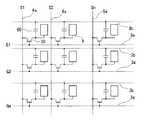
図1〜図4に基づいて、本発明に係る実施例1の電気光学装置の構造について説明する。本実施形態では、スイッチング素子としてLDD構造のダブルゲートTFT(薄膜半導体装置)を用いたアクティブマトリクス型の透過型液晶装置(電気光学装置)を例にとり説明する。
図1は本実施例の液晶装置の画像表示領域を構成するマトリクス状に配置された複数のドットにおけるスイッチング素子、信号線等の等価回路図、図2はデータ線、走査線、画素電極等が形成されたTFTアレイ基板の1ドットを拡大して示す平面図、図3は本実施例の液晶装置の構造を示す断面図であって、図2のA−A’線に沿う断面図、図4はLDD構造のダブルゲートTFTを示す断面図である。なお、図3においては、図示上側が光入射側、図示下側が視認側(観察者側)である場合について図示している。また、各図においては、各層や各部材を図面上で認識可能な程度の大きさとするため、各層や各部材毎に縮尺を異ならせてある。The structure of the electro-optical device according to the first embodiment of the present invention will be described with reference to FIGS. In this embodiment, an active matrix transmissive liquid crystal device (electro-optical device) using a double gate TFT (thin film semiconductor device) having an LDD structure as a switching element will be described as an example.
FIG. 1 is an equivalent circuit diagram of switching elements, signal lines and the like in a plurality of dots arranged in a matrix constituting the image display area of the liquid crystal device of this embodiment, and FIG. 2 is a diagram showing data lines, scanning lines, pixel electrodes and the like. 3 is an enlarged plan view showing one dot of the formed TFT array substrate, FIG. 3 is a cross-sectional view showing the structure of the liquid crystal device of this embodiment, and is a cross-sectional view taken along the line AA ′ of FIG. 4 is a cross-sectional view showing a double gate TFT having an LDD structure. Note that FIG. 3 illustrates the case where the upper side in the drawing is the light incident side and the lower side in the drawing is the viewing side (observer side). Moreover, in each figure, in order to make each layer and each member the size which can be recognized on drawing, the scale is varied for every layer and each member.
本実施例の液晶装置において、図1に示すように、画像表示領域を構成するマトリクス状に配置された複数のドットには、画素電極9と当該画素電極9を制御するためのスイッチング素子であるLDD構造のダブルゲートTFT(薄膜半導体装置)30がそれぞれ形成されており、画像信号が供給されるデータ線6aが当該TFT30のソースに電気的に接続されている。データ線6aに書き込む画像信号S1、S2、…、Snは、この順に線順次に供給されるか、あるいは相隣接する複数のデータ線6aに対してグループ毎に供給される。 In the liquid crystal device of the present embodiment, as shown in FIG. 1, a plurality of dots arranged in a matrix that forms an image display area are
また、走査線3aがTFT30のゲートに電気的に接続されており、複数の走査線3aに対して走査信号G1、G2、…、Gmが所定のタイミングでパルス的に線順次で印加される。また、画素電極9はTFT30のドレインに電気的に接続されており、スイッチング素子であるTFT30を一定期間だけオンすることにより、データ線6aから供給される画像信号S1、S2、…、Snを所定のタイミングで書き込む。 Further, the
画素電極9を介して液晶に書き込まれた所定レベルの画像信号S1、S2、…、Snは、後述する共通電極との間で一定期間保持される。液晶は、印加される電圧レベルにより分子集合の配向や秩序が変化することにより、光を変調し、階調表示を可能にする。ここで、保持された画像信号がリークすることを防止するために、画素電極9と共通電極との間に形成される液晶容量と並列に蓄積容量60が付加されている。 A predetermined level of image signals S1, S2,..., Sn written to the liquid crystal via the
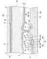
図3に示すように、本実施例の液晶装置は、液晶層50を挟持して対向配置され、TFT30や画素電極9が形成されたTFTアレイ基板10と、共通電極21が形成された対向基板20とを具備して概略構成されている。 As shown in FIG. 3, the liquid crystal device of this embodiment is arranged so as to face each other with a
以下、TFTアレイ基板10の平面構造について図2に基づき説明する。
TFTアレイ基板10には、矩形状の画素電極9が複数、マトリクス状に設けられており、各画素電極9の縦横の境界に沿って、データ線6a、走査線3a及び容量線3bが設けられている。本実施例において、各画素電極9及び各画素電極9を囲むように配設されたデータ線6a、走査線3a等が形成された領域が1ドットとなっている。Hereinafter, the planar structure of the
A plurality of
データ線6aは、TFT30を構成する多結晶シリコンからなる半導体薄膜35のうちソース領域35xに、コンタクトホール13を介して電気的に接続されており、画素電極9は、半導体薄膜35のうちドレイン領域35yに、コンタクトホール15、ソース線6b、コンタクトホール14を介して電気的に接続されている。また、走査線3aの一部が半導体薄膜35のうちチャネル領域35aに対向するように拡幅されており、走査線3aの拡幅された部分が、下部ゲート電極33及び上部ゲート電極37として機能する。以下、走査線3aにおいて、ゲート電極として機能する部分を単に「ゲート電極」と称し、符号3cで示す。また、TFT30を構成する半導体薄膜35は、容量線3bと対向する部分にまで延設されており、この延設部分35fを下電極、容量線3bを上電極とする蓄積容量(蓄積容量素子)60が形成されている。 The
次に、図3に基づいて、本実施例の液晶装置の断面構造について説明する。
TFTアレイ基板10は、ガラス等の透光性材料からなる基板本体(透光性基板)10Aとその液晶層50側表面に形成された画素電極9、TFT30、配向膜12を主体として構成されており、対向基板20はガラス等の透光性材料からなる基板本体20Aとその液晶層50側表面に形成された共通電極21と配向膜22とを主体として構成されている。Next, the cross-sectional structure of the liquid crystal device of this embodiment will be described with reference to FIG.
The
詳細には、TFTアレイ基板10において、基板本体10Aの直上に、シリコン酸化膜等の絶縁材料からなる下地保護膜を兼ねる下部ゲート絶縁膜(第1の絶縁膜)34が形成されている。また、基板本体10Aの液晶層50側表面にはインジウム錫酸化物(ITO)等の透明導電性薄膜からなる画素電極9が設けられ、各画素電極9に隣接する位置に、各画素電極9をスイッチング制御する画素スイッチング用のTFT30が設けられている。
なお、本実施例では、透過型液晶装置を例としたので、画素電極9はITO等の透明導電性薄膜からなるが、反射型液晶装置では、画素電極9はAl等の金属薄膜からなり、反射半透過型液晶装置では、ITO等の透明導電性薄膜とAl等の金属薄膜の積層構造からなる。Specifically, in the
In this embodiment, since the transmissive liquid crystal device is taken as an example, the
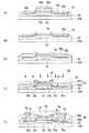
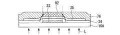
この画素スイッチング用のTFT30は、nチャネル型またはpチャネル型のLDD構造のダブルゲートTFT(Thin-Film Transistor)(薄膜半導体装置)であり、図4に示すように、透光性を有する基板本体(透光性基板)10A上に、アルミニウム、タンタル、モリブデン、チタン、クロム、あるいはこれらの金属を成分とする合金等の遮光性を有する所定パターンの導電膜からなる下部ゲート電極(第1のゲート電極)33、酸化珪素、窒化珪素等からなる下部ゲート絶縁膜(第1の絶縁膜)34、多結晶シリコンからなる島状の半導体薄膜35、酸化珪素、窒化珪素等からなる上部ゲート絶縁膜(第2の絶縁膜)36、アルミニウム、タンタル、モリブデン、チタン、クロム、あるいはこれらの金属を成分とする合金等の遮光性を有する所定パターンの導電膜からなる上部ゲート電極(第2のゲート電極)37、酸化珪素、窒化珪素等からなる層間絶縁膜38が積層されている。 This
半導体薄膜35は、チャネル領域35aと、このチャネル領域35aの両側それぞれに形成されたソース領域35x及びドレイン領域35yとを備えている。
このソース領域35xは、チャネル領域35a側の不純物濃度が相対的に低い低濃度ソース領域35bと、この低濃度ソース領域35bに隣接して形成された不純物濃度が相対的に高い高濃度ソース領域35dとを備えている。また、ドレイン領域35yは、チャネル領域35a側の不純物濃度が相対的に低い低濃度ドレイン領域35cと、この低濃度ドレイン領域35cに隣接して形成された不純物濃度が相対的に高い高濃度ドレイン領域35eとを備えている。The semiconductor
The
この上部ゲート絶縁膜37上には、走査線3a(ゲート電極3c)が形成され、本実施例では、ゲート電極3cの側面は上部ゲート絶縁膜36の表面に対して略垂直となっている。また、半導体薄膜35のうち、下部ゲート絶縁膜34を介して下部ゲート電極33と対向する領域、及び上部ゲート絶縁膜37を介して上部ゲート電極37と対向する領域が、下部ゲート電極33及び上部ゲート電極37それぞれからの電界によりチャネルが形成されるチャネル領域35aとなっている。 A
このチャネル領域35aには、下部ゲート絶縁膜34を介して下部ゲート電極33が対向配置されるとともに、上部ゲート絶縁膜36を介して上部ゲート電極37が対向配置されている。
上部ゲート絶縁膜36は、第1絶縁層36a及び第2絶縁層36bの2層構造からなるもので、第1絶縁層6aには、チャネル領域35aの中央部に対応する部分に開口部39が形成され、これによって、上部ゲート絶縁膜36のチャネル領域35aの中央部に対応する部分の厚みが、このチャネル領域35aのソース・ドレイン端、すなわち低濃度ソース領域35b及び低濃度ドレイン領域35c近傍に対応する部分の厚みより薄くなるようになっている。A
The upper
また、走査線3a(ゲート電極3c)が形成された基板本体10A上には、シリコン酸化膜等からなる層間絶縁膜38が形成されており、この層間絶縁膜38上に、データ線6a及びソース線6bが形成されている。データ線6aは層間絶縁膜38に形成されたコンタクトホール13を介して半導体薄膜35の高濃度ソース領域35dに電気的に接続されており、ソース線6bは、層間絶縁膜38に形成されたコンタクトホール14を介して半導体薄膜35の高濃度ドレイン領域35eに電気的に接続されている。 An interlayer insulating
また、データ線6a、ソース線6bが形成された層間絶縁膜38上には、シリコン窒化膜等からなる第2層間絶縁膜5が形成されており、第2層間絶縁膜5上に、画素電極9が形成されている。画素電極9は、第2層間絶縁膜5に形成されたコンタクトホール15を介して、ソース線6bに電気的に接続されている。
また、半導体薄膜35の高濃度ドレイン領域35eからの延設部分35f(下電極)に対して、上部ゲート絶縁膜37と一体形成された絶縁膜(誘電体膜)を介して、走査線3aと同層に形成された容量線3bが上電極として対向配置されており、これら延設部分35fと容量線3bにより蓄積容量60が形成されている。
また、TFTアレイ基板10の液晶層50側最表面には、液晶層50内の液晶分子の配列を制御するための配向膜12が形成されている。A second interlayer insulating film 5 made of a silicon nitride film or the like is formed on the
Further, the
An
他方、対向基板20においては、基板本体20Aの液晶層50側表面に、液晶装置に入射した光が、少なくとも、半導体薄膜35のチャネル領域35a、低濃度ソース領域35b及び低濃度ドレイン領域35cに入射するのを防止するための遮光膜23が形成されている。また、遮光膜23が形成された基板本体20A上には、そのほぼ全面に渡って、ITO等からなる共通電極21が形成され、その液晶層50側には、液晶層50内の液晶分子の配列を制御するための配向膜22が形成されている。 On the other hand, in the
このTFT30では、上部ゲート絶縁膜36のチャネル領域35aの中央部付近の厚みが、チャネル領域35aのソース・ドレイン端付近の厚みより薄くなっていることにより、下部ゲート電極33及び上部ゲート電極37によりチャネル領域35aに電圧を印加した場合に、電界は上部ゲート電極37から上部ゲート絶縁膜36のうち厚みの薄い部分を介してチャネル領域35aの中央部付近に集中し、下部ゲート電極33から下部ゲート絶縁膜34を介してチャネル領域35aの中央部付近に集中する。これにより、チャネル領域35aの周辺部分すなわちソース・ドレイン端近傍の電界強度が緩和される。 In the
以上説明したように、このダブルゲートTFT30によれば、チャネル領域35aのソース・ドレイン端近傍の電界強度が緩和されるので、オフリーク電流を低減することができ、さらに、耐圧性及び信頼性を向上させることができる。
また、ゲート電圧に対する耐性あるいはドレイン電圧に対する耐性等の耐圧性を向上させることができ、信頼性を向上させることができる。
また、チャネル領域35aの下方に下部ゲート電極33を、上方に上部ゲート電極37を、それぞれ対向配置したので、チャネルの構造を上下それぞれにチャネルを有するダブルチャネル構造とすることができ、したがって、単位面積当たりの電流密度を高くすることができ、オン電流を増大させることができる。
さらに、LDD構造としたので、ゲート電圧に対する耐性あるいはドレイン電圧に対する耐性等の耐圧性を向上させることができ、信頼性を向上させることができる。As described above, according to the
In addition, withstand voltage characteristics such as resistance to gate voltage or drain voltage can be improved, and reliability can be improved.
Further, since the
In addition, since the LDD structure is employed, it is possible to improve withstand voltage properties such as resistance to gate voltage or resistance to drain voltage, and reliability can be improved.
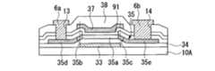
図5は、本発明の実施例2のnチャネル型のLDD構造のダブルゲートTFT(Thin-Film Transistor)(薄膜半導体装置)を示す断面図である。
このダブルゲートTFTが、実施例1のダブルゲートTFTと異なる点は、実施例1のダブルゲートTFTでは、第1絶縁層36aのチャネル領域35aの中央部に対応する位置に単に開口部39を形成しただけであるのに対し、本実施例2のダブルゲートTFTでは、第1絶縁層36aのチャネル領域35aの中央部に対応する位置に、下部ゲート電極33と同じ大きさの開口部71を形成した点であり、それ以外の構成要素については実施例1のダブルゲートTFTと全く同様である。FIG. 5 is a cross-sectional view showing an n-channel LDD structure double gate TFT (Thin-Film Transistor) (thin film semiconductor device) according to a second embodiment of the present invention.
This double gate TFT is different from the double gate TFT of the first embodiment in that, in the double gate TFT of the first embodiment, an
このダブルゲートTFTでは、第1絶縁層36aのチャネル領域35aの中央部に対応する位置に、下部ゲート電極33と同じ大きさの開口部71を形成したので、下部ゲート電極33及び上部ゲート電極37によりチャネル領域35aに電圧を印加した場合に、電界は上部ゲート電極37から第1絶縁層36aの開口部71を介してチャネル領域35aの中央部付近に集中し、下部ゲート電極33から下部ゲート絶縁膜34を介してチャネル領域35aの中央部付近に集中する。
これにより、チャネル領域35aの周辺部分であるソース・ドレイン端近傍の電界強度が緩和される。In this double gate TFT, the
As a result, the electric field strength in the vicinity of the source / drain end, which is the peripheral portion of the
また、チャネル領域35aの下方に下部ゲート電極33を、上方に上部ゲート電極37を、それぞれ対向配置したことにより、チャネルの構造が半導体薄膜35の上下面それぞれにチャネルを有するダブルチャネル構造となる。これにより、単位面積当たりの電流密度が高まり、オン電流が大きく増大する。 Further, the
次に、このダブルゲートTFTの製造方法について、図6及び図7に基づき説明する。
まず、図6(a)に示すように、表面を超音波洗浄等により清浄化したガラス基板等からなる透光性を有する基板本体10Aを用意し、この基板本体10A全面に、スパッタリング法等によりアルミニウム、タンタル、モリブデン、チタン、クロム等の金属、またはこれらの金属のいずれかを主成分とする合金等からなる遮光性を有する10〜500nmの厚みの導電膜72を形成し、その後、この導電膜72をフォトリソグラフィー法によりパターニングし、所定形状にパターニングされた遮光性を有する下部ゲート電極33とする。この下部ゲート電極33のパターンエッジになだらかな傾斜を持たせてテーパー形状にすると、その後の工程で、薄膜を形成する時に、この下部ゲート電極33上の薄膜の被覆性が向上する。Next, a method for manufacturing the double gate TFT will be described with reference to FIGS.
First, as shown in FIG. 6A, a
次いで、この下部ゲート電極33を含む基板本体10A上に、プラズマCVD法等により、基板温度が100〜600℃となる条件下で、酸化珪素(SiO2)、窒化珪素(Si3N4)等からなる10〜50nmの厚みの下部ゲート絶縁膜34を成膜する。
この成膜工程に用いられる原料としては、モノシラン(SiH4)と一酸化二窒素(N2O)との混合ガス、ジシラン(Si2H6)とアンモニア(NH3)との混合ガス、テトラエトキシシラン(TEOS:Si(OC2H5)4)と酸素(O2)との混合ガス等が好適である。Next, silicon oxide (SiO2 ), silicon nitride (Si3 N4 ) or the like is formed on the substrate
The raw material used in this film forming process includes a mixed gas of monosilane (SiH4 ) and dinitrogen monoxide (N2 O), a mixed gas of disilane (Si2 H6 ) and ammonia (NH3 ), tetra A mixed gas of ethoxysilane (TEOS: Si (OC2 H5 )4 ) and oxygen (O2 ) is preferable.
次いで、図6(b)に示すように、下部ゲート絶縁膜34上に、プラズマCVD法等により、基板温度が100〜600℃となる条件下で、非晶質シリコン(a−Si)からなる10〜100nmの厚みの非晶質半導体薄膜73を成膜する。
この成膜工程に用いられる原料としては、モノシラン(SiH4)、ジシラン(Si2H6)等が好適である。
次いで、この非晶質半導体薄膜73にレーザ光を照射する等して加熱することにより多結晶化し、多結晶シリコンからなる多結晶半導体薄膜74とする。その他にも、400〜700℃程度でアニールすることにより非晶質半導体薄膜73を多結晶化する固相成長法を用いてもよい。
次いで、フォトリソグラフィ法により多結晶半導体薄膜74をパターニングし、島状の半導体薄膜35とする。Next, as shown in FIG. 6B, the lower
Monosilane (SiH4 ), disilane (Si2 H6 ), and the like are suitable as raw materials used in this film forming process.
Next, the amorphous semiconductor
Next, the polycrystalline semiconductor thin film 74 is patterned by a photolithography method to form an island-shaped semiconductor
次いで、図6(c)に示すように、この半導体薄膜35を含む下部ゲート絶縁膜34上に、ポジ型フォトレジスト76を塗布し、下部ゲート電極33をマスクとして基板本体10Aの裏面側(下部ゲート電極33と反対側)から光Lを照射し、このフォトレジスト76を露光する。
次いで、このフォトレジスト76を現像し、このフォトレジスト76に所定形状のパターニングを施す。これにより、図6(d)に示すように、フォトレジスト76は、下部ゲート電極33と同じ大きさの島状のフォトレジスト76aを除いて除去される。Next, as shown in FIG. 6C, a
Next, the
ここでは、このフォトレジスト76に下部ゲート電極33と同じ大きさの島状のフォトレジストを形成するために、このフォトレジスト76に適切な露光が行われる様に、光Lの光強度及び露光時間を適切に制御する必要がある。これにより、フォトレジスト76は下部ゲート電極33に対応する領域のみを除いて露光され、フォトレジスト76の硬化領域は下部ゲート電極33と同じ大きさとなる。
このフォトレジスト76を現像することにより、このフォトレジスト76に下部ゲート電極33と同じ大きさの島状のフォトレジスト76aが形成される。Here, in order to form an island-shaped photoresist having the same size as that of the
By developing the
次いで、図6(e)に示すように、島状のフォトレジスト76aをマスクとして、半導体薄膜35に上方より約0.1×10¹³〜10×1013/cm2のドーズ量で低濃度の不純物イオン(リン(P)イオンまたはボロン(B)イオン)77を注入する。
この低濃度の不純物イオン77注入により、半導体薄膜35のうちフォトレジスト76aに覆われていない部分は上部ゲート電極33に対して自己整合的に低濃度のソース領域35b及びドレイン領域35cが形成され、フォトレジスト76aに覆われている部分は不純物イオン77注入が成されないのでチャネル領域35aとなる。Next, as shown in FIG. 6E, with the island-shaped
By this low-
次いで、図7(f)に示すように、島状のフォトレジスト76a及び半導体薄膜35を含む下部ゲート絶縁膜34上に、プラズマCVD法等により、基板温度が100〜600℃となる条件下で、酸化珪素(SiO2)、窒化珪素(Si3N4)等からなる20〜1000nmの厚みの第1絶縁層36aを成膜する。
この成膜工程に用いられる原料は、下部ゲート絶縁膜34と全く同様である。
この結果、島状のフォトレジスト76a上、及びこの島状のフォトレジスト76a上を除く半導体薄膜35及び下部ゲート絶縁膜34上それぞれに、第1絶縁層36aが成膜されることとなる。Next, as shown in FIG. 7F, on the lower
The raw material used in this film forming process is exactly the same as that of the lower
As a result, the first insulating
次いで、リフトオフ法により、島状のフォトレジスト76aと該島状のフォトレジスト76上の第1絶縁層36aを除去する。
これにより、図7(g)に示すように、半導体薄膜35及び下部ゲート絶縁膜34上に、島状のフォトレジスト76aと平面視同一形状の開口部71を有する第1絶縁層36aが形成されることとなる。
次いで、図7(h)に示すように、半導体薄膜35を含む第1絶縁層36a上に、プラズマCVD法等により、基板温度が100〜600℃となる条件下で、酸化珪素(SiO2)、窒化珪素(Si3N4)等からなる20〜1000nmの厚みの第2絶縁層36bを成膜する。
この成膜工程に用いられる原料は、下部ゲート絶縁膜34と全く同様である。これら第1絶縁層36a及び第2絶縁層36bにより上部ゲート絶縁膜36が構成される。Next, the island-
As a result, as shown in FIG. 7G, the first insulating
Next, as shown in FIG. 7H, silicon oxide (SiO2 ) is formed on the first insulating
The raw material used in this film forming process is exactly the same as that of the lower
次いで、図7(i)に示すように、第2絶縁層36b全面に、スパッタリング法等によりアルミニウム、タンタル、モリブデン、チタン、クロム等の金属、またはこれらの金属のいずれかを主成分とする合金等からなる10〜500nmの厚みの導電膜79を形成し、その後、この導電膜79をフォトリソグラフィー法によりパターニングし、上部ゲート電極37より幅が広くかつ半導体薄膜35より幅が狭い上部ゲート電極37とする。 Next, as shown in FIG. 7 (i), a metal such as aluminum, tantalum, molybdenum, titanium, or chromium, or an alloy containing any of these metals as a main component is formed on the entire surface of the second insulating
次いで、上部ゲート電極37をマスクとして、半導体薄膜35に上方より約0.1×10¹⁵〜10×1015/cm2のドーズ量で高濃度の不純物イオン(リン(P)イオンまたはボロン(B)イオン)81を注入する。
この高濃度の不純物イオン81注入により、半導体薄膜35のうち上部ゲート電極37に覆われていない部分は上部ゲート電極37に対して自己整合的に高濃度のソース領域35d及びドレイン領域35eが形成される。なお、上部ゲート電極37に覆われている部分は高濃度の不純物イオン81注入が成されないので、低濃度のソース領域35b、ドレイン領域35c及びチャネル領域35aのままである。Next, high-concentration impurity ions (phosphorus (P) ions or boron (B) with a dose of about 0.1 × 10¹⁵ to 10 × 1015 / cm2 from above are formed on the semiconductor
By this high
次いで、図7(j)に示すように、上部ゲート電極37を含む第2絶縁層36b上に、プラズマCVD法等により、基板温度が100〜600℃となる条件下で、酸化珪素(SiO2)、窒化珪素(Si3N4)等からなる100〜1000nmの厚みの層間絶縁膜38を成膜する。この成膜工程に用いられる原料は、下部ゲート絶縁膜34、第1絶縁層36a及び第2絶縁層36bと全く同様である。
次いで、層間絶縁膜38上に所定形状のフォトレジスト(図示略)を形成し、このフォトレジストをマスクとして上部ゲート絶縁膜36及び層間絶縁膜38にドライエッチングを施し、これら上部ゲート絶縁膜36及び層間絶縁膜38に、高濃度ソース領域35dに達するコンタクトホール13及び高濃度ドレイン領域35eに達するコンタクトホール14をそれぞれ形成する。Next, as shown in FIG. 7J, silicon oxide (SiO2 ) is formed on the second insulating
Next, a photoresist (not shown) having a predetermined shape is formed on the
次いで、層間絶縁膜38全面に、スパッタリング法等により、アルミニウム、タンタル、モリブデン、チタン、クロム等の金属、あるいはこれらの金属のうち少なくとも1種を含む合金等からなる導電膜を形成し、その後、この導電膜をフォトリソグラフィ法によりパターニングし、ソース電極6a及びドレイン電極6bとする。
以上により、nチャネル型またはpチャネル型のLDD構造のダブルゲートTFTを作製することができる。Next, a conductive film made of a metal such as aluminum, tantalum, molybdenum, titanium, or chromium, or an alloy containing at least one of these metals is formed on the entire surface of the
As described above, a double-gate TFT having an n-channel or p-channel LDD structure can be manufactured.
以上説明した様に、このLDD構造のダブルゲートTFTによれば、第1絶縁層36aのチャネル領域35aの中央部に対応する位置に、下部ゲート電極33と同じ大きさの開口部71を形成したので、下部ゲート電極33及び上部ゲート電極37によりチャネル領域35aに電圧を印加した場合に、電界は上部ゲート電極37から第1絶縁層36aの開口部71を介してチャネル領域35aの中央部付近に集中し、下部ゲート電極33から下部ゲート絶縁膜34を介してチャネル領域35aの中央部付近に集中することとなり、チャネル領域35aのソース・ドレイン端近傍の電界強度が緩和される。したがって、オフリーク電流を低減することができ、さらに、耐圧性及び信頼性を向上させることができる。 As described above, according to the double gate TFT having the LDD structure, the
また、チャネル領域4aの下方に下部ゲート電極2を、上方に上部ゲート電極6を、それぞれ対向配置したので、チャネルの構造を上下それぞれにチャネルを有するダブルチャネル構造とすることができる。したがって、チャネル領域4aの中央部へ電流を集中させることができ、オン電流を増大させることができる。
さらに、LDD構造としたので、ゲート電圧に対する耐性あるいはドレイン電圧に対する耐性等の耐圧性を向上させることができ、信頼性を向上させることができる。Further, since the
In addition, since the LDD structure is employed, it is possible to improve withstand voltage properties such as resistance to gate voltage or resistance to drain voltage, and reliability can be improved.
また、このダブルゲートTFTの製造方法によれば、半導体薄膜35を含む下部ゲート絶縁膜34上に、ポジ型フォトレジスト76を塗布し、下部ゲート電極33をマスクとして基板本体10Aの裏面側から光Lを照射し、このフォトレジスト76を露光して島状のフォトレジスト76aとし、このフォトレジスト76aを含む全面に第1絶縁層36aを成膜し、リフトオフ法により、島状のフォトレジスト76aと該島状のフォトレジスト76上の第1絶縁層36aを除去するので、第1絶縁層36aのチャネル領域35aの中央部に対応する位置に、下部ゲート電極33と同じ大きさの開口部71を形成することができ、オフリーク電流を低減するとともに、オン電流を増大させることができ、さらに、耐圧性及び信頼性を向上させることができるLDD構造のダブルゲートTFTを、容易にかつ低コストで作製することができる。 Further, according to this method for manufacturing a double gate TFT, a
図8は、本発明の実施例3のnチャネル型のLDD構造のダブルゲートTFTの製造方法を示す過程図であり、この製造方法により上述した実施例2のnチャネル型のLDD構造のダブルゲートTFTが得られる。
このダブルゲートTFTの製造方法について、図8に基づき説明する。
この製造方法においては、半導体薄膜35上に下部ゲート電極33と同じ大きさの島状のフォトレジスト76aを形成するまでは、上記実施例2と全く同様である。FIG. 8 is a process diagram showing a method of manufacturing an n-channel type LDD structure double gate TFT according to the third embodiment of the present invention. By this manufacturing method, the n-channel LDD structure double gate according to the second embodiment described above. A TFT is obtained.
A method for manufacturing the double gate TFT will be described with reference to FIG.
This manufacturing method is exactly the same as that of the second embodiment until the island-shaped
その後、図8(a)に示すように、島状のフォトレジスト76a及び半導体薄膜35を含む下部ゲート絶縁膜34上に、プラズマCVD法等により、基板温度が100〜600℃となる条件下で、酸化珪素(SiO2)、窒化珪素(Si3N4)等からなる20〜1000nmの厚みの第1絶縁層36aを成膜する。
この成膜工程に用いられる原料は、下部ゲート絶縁膜34と全く同様である。
この結果、島状のフォトレジスト76a上、及びこの島状のフォトレジスト76a上を除く半導体薄膜35及び下部ゲート絶縁膜34上それぞれに、第1絶縁層36aが成膜されることとなる。Thereafter, as shown in FIG. 8A, on the lower
The raw material used in this film forming process is exactly the same as that of the lower
As a result, the first insulating
次いで、図8(b)に示すように、島状のフォトレジスト76a及び第1絶縁層36aをマスクとして、半導体薄膜35に上方より約0.1×10¹³〜10×1013/cm2のドーズ量で低濃度の不純物イオン(リン(P)イオンまたはボロン(B)イオン)77を注入する。
この低濃度の不純物イオン77注入により、半導体薄膜35のうち第1絶縁層36aのみにより覆われている部分は上部ゲート電極33に対して自己整合的に低濃度のソース領域35b及びドレイン領域35cが形成され、フォトレジスト76a及び第1絶縁層36aに覆われている部分は不純物イオン77注入が成されないのでチャネル領域35aとなる。Next, as shown in FIG. 8B, the island-shaped
By this low
リフトオフ法により、島状のフォトレジスト76aと該島状のフォトレジスト76上の第1絶縁層36aを除去する工程以降は、実施例2のダブルゲートTFTの製造方法と全く同様である。
このダブルゲートTFTの製造方法においても、実施例2のダブルゲートTFTの製造方法と全く同様、オフリーク電流を低減することができ、オン電流を増大させることができ、耐圧性及び信頼性を向上させることができるダブルゲートTFTを、容易にかつ低コストで作製することができる。After the step of removing the island-
Also in this double gate TFT manufacturing method, the off-leakage current can be reduced, the on-current can be increased, and the withstand voltage and the reliability can be improved, just like the double gate TFT manufacturing method of the second embodiment. A double-gate TFT that can be manufactured can be easily manufactured at low cost.
図9は、本発明の実施例4のnチャネル型またはpチャネル型のLDD構造のダブルゲートTFT(Thin-Film Transistor)(薄膜半導体装置)を示す断面図である。
このダブルゲートTFTが、実施例2のダブルゲートTFTと異なる点は、実施例2のダブルゲートTFTでは、第1絶縁層36aのチャネル領域35aの中央部に対応する位置に、下部ゲート電極33と同じ大きさの開口部71を形成したのに対し、本実施例4のダブルゲートTFTでは、第1絶縁層36aのチャネル領域35aの中央部に対応する位置に、下部ゲート電極33より幅が狭い開口部91を形成した点であり、それ以外の構成要素については実施例2のTFTと全く同様である。FIG. 9 is a cross-sectional view showing an n-channel or p-channel LDD double-gate TFT (Thin-Film Transistor) (thin film semiconductor device) according to a fourth embodiment of the present invention.
This double gate TFT is different from the double gate TFT of the second embodiment in that, in the double gate TFT of the second embodiment, the
このダブルゲートTFTでは、第1絶縁層36aのチャネル領域35aの中央部に対応する位置に、下部ゲート電極33より幅が狭い開口部91を形成したことにより、下部ゲート電極33及び上部ゲート電極37によりチャネル領域35aに電圧を印加した場合に、電界は上部ゲート電極37から第1絶縁層36aの開口部91を介してチャネル領域35aの中央部付近に集中し、下部ゲート電極33から下部ゲート絶縁膜34を介してチャネル領域35aの中央部付近に集中する。 In this double gate TFT, an
これにより、チャネル領域35aのソース・ドレイン端近傍の電界強度が緩和され、オフリーク電流が大きく低減され、さらに、耐圧性及び信頼性がさらに向上する。
また、チャネル領域35aの下方に下部ゲート電極33を、上方に上部ゲート電極37を、それぞれ対向配置したことにより、チャネルの構造が上下それぞれにチャネルを有するダブルチャネル構造となり、単位面積当たりの電流密度が高まり、オン電流が増大する。As a result, the electric field strength in the vicinity of the source / drain ends of the
Further, the
このダブルゲートTFTの製造方法は、ポジ型フォトレジスト76の露光条件を除いて上記実施例2と全く同様である。
この露光条件は、上記実施例2では、露光過多や露光不足にならない適切な露光条件を選択したのに対し、本実施例では、光強度、露光時間の少なくとも一方を大きくする「露光過多」を選択する。露光過多の場合、図10に示すように、マスクとなる下部ゲート電極33の裏側に回り込む光Lの光量が増加し、ポジ型フォトレジスト76の硬化領域92は下部ゲート電極33の幅より狭くなる。よって、島状のポジ型フォトレジスト76aとなるフォトレジスト76の硬化領域92は下部ゲート電極33の幅より狭くなる。The manufacturing method of this double gate TFT is exactly the same as that of the second embodiment except for the exposure condition of the
As for the exposure conditions, in Example 2 described above, appropriate exposure conditions that do not cause overexposure or underexposure are selected, whereas in this embodiment, “overexposure” that increases at least one of light intensity and exposure time is set. select. In the case of overexposure, as shown in FIG. 10, the amount of light L that wraps around the back side of the
したがって、フォトレジスト76を露光過多とすることにより、下部ゲート電極33より幅の狭い島状のポジ型フォトレジストを形成することができ、この島状のポジ型フォトレジストを用いて、第1絶縁層36aのチャネル領域35aの中央部に対応する位置に、下部ゲート電極33より幅が狭い開口部91を形成することができる。 Therefore, by making the
このダブルゲートTFTによれば、第1絶縁層36aのチャネル領域35aの中央部に対応する位置に、下部ゲート電極33より幅が狭い開口部91を形成したので、オフリーク電流を低減することができ、オン電流を大きく増大させることができ、耐圧性及び信頼性をさらに向上させることができる。 According to this double gate TFT, since the
図11は、本発明の実施例5のnチャネル型またはpチャネル型のLDD構造のダブルゲートTFT(Thin-Film Transistor)(薄膜半導体装置)を示す断面図である。
このダブルゲートTFTが、実施例2のダブルゲートTFTと異なる点は、実施例2のダブルゲートTFTでは、第1絶縁層36aのチャネル領域35aの中央部に対応する位置に、下部ゲート電極33と同じ大きさの開口部71を形成したのに対し、本実施例5のダブルゲートTFTでは、第1絶縁層36aのチャネル領域35aの中央部に対応する位置に、下部ゲート電極33より幅が広い開口部101を形成した点であり、それ以外の構成要素については実施例2のTFTと全く同様である。FIG. 11 is a sectional view showing an n-channel or p-channel LDD structure double gate TFT (Thin-Film Transistor) (thin film semiconductor device) of Example 5 of the present invention.
This double gate TFT is different from the double gate TFT of the second embodiment in that, in the double gate TFT of the second embodiment, the
このダブルゲートTFTでは、チャネル領域35aのソース・ドレイン端近傍の電界強度が緩和され、オフリーク電流が大きく低減され、さらに、耐圧性及び信頼性がさらに向上する。
また、チャネル領域35aの下方に下部ゲート電極33を、上方に上部ゲート電極37を、それぞれ対向配置したことにより、チャネルの構造が上下それぞれにチャネルを有するダブルチャネル構造となり、単位面積当たりの電流密度が高まり、オン電流が増大する。In this double gate TFT, the electric field strength in the vicinity of the source / drain end of the
Further, the
このダブルゲートTFTの製造方法は、ポジ型フォトレジスト76の露光条件を除いて上記実施例2と全く同様である。
この露光条件は、上記実施例2では、露光過多や露光不足にならない適切な露光条件を選択したのに対し、本実施例では、光強度、露光時間の少なくとも一方を小さくする「露光不足」を選択する。露光不足の場合、図12に示すように、マスクとなる下部ゲート電極33の裏側には光Lが回り込まず、ポジ型フォトレジスト76の硬化領域92は下部ゲート電極33の幅より広くなる。よって、島状のポジ型フォトレジスト76aとなるフォトレジスト76の硬化領域92は下部ゲート電極33の幅より広くなる。The manufacturing method of this double gate TFT is exactly the same as that of the second embodiment except for the exposure condition of the
As for the exposure conditions, in Example 2 described above, appropriate exposure conditions that do not cause overexposure or underexposure are selected, whereas in this embodiment, “underexposure” that reduces at least one of light intensity and exposure time is reduced. select. In the case of underexposure, as shown in FIG. 12, the light L does not enter the back side of the
したがって、この露光不足のフォトレジスト76を現像することにより、このフォトレジスト76の非硬化領域が除去されるので、下部ゲート電極33より幅の広い島状のポジ型フォトレジストが形成されることとなる。
また、露光条件によらず、露光後の現像処理時間を長くしたり、あるいは、現像時の現像液の温度を通常よりも高くすることで、同様に、下部ゲート電極33より幅の広い島状のポジ型フォトレジストが形成される。本発明においては、いずれの方法を用いてもよい。Therefore, by developing the underexposed
Also, regardless of the exposure conditions, by increasing the development processing time after exposure, or by increasing the temperature of the developing solution during development, the island shape is wider than the
このダブルゲートTFTによれば、第1絶縁層36aのチャネル領域35aの中央部に対応する位置に、下部ゲート電極33より幅が広い開口部101を形成したので、オフリーク電流をさらに低減することができ、オン電流を増大させることができ、耐圧性及び信頼性をさらに向上させることができる。 According to the double gate TFT, since the
図13は、本発明の実施例6のnチャネル型またはpチャネル型のLDD構造のダブルゲートTFT(Thin-Film Transistor)(薄膜半導体装置)を示す断面図である。
このダブルゲートTFTが、実施例1のダブルゲートTFTと異なる点は、実施例1のダブルゲートTFTでは、上部ゲート絶縁膜36を第1及び第2絶縁層36a、36bの2層構造とし、第1絶縁層36aのチャネル領域35aの中央部に対応する位置に開口部39を形成したのに対し、本実施例6のダブルゲートTFTでは、上部ゲート絶縁膜(第2の絶縁膜)を単層構造とし、この上部ゲート絶縁膜111の厚みを、チャネル領域35aの中央部に対応する中央部分111aの厚みが、このチャネル領域35aのソース・ドレイン端近傍に対応する周辺部分111bの厚みより薄くなるようにした点であり、それ以外の構成要素については実施例1のダブルゲートTFTと全く同様である。FIG. 13 is a cross-sectional view showing an n-channel or p-channel LDD structure double gate TFT (Thin-Film Transistor) (thin film semiconductor device) according to
This double gate TFT differs from the double gate TFT of the first embodiment in that the upper
このダブルゲートTFTでは、上部ゲート絶縁膜111の厚みを、チャネル領域35aの中央部に対応する中央部分111aの厚みが、このチャネル領域35aのソース・ドレイン端近傍に対応する周辺部分111bの厚みより薄くなるようにしたので、オフリーク電流が低減され、さらに、耐圧性及び信頼性が向上する。
また、チャネルの構造が上下それぞれにチャネルを有するダブルチャネル構造となり、単位面積当たりの電流密度が高まり、オン電流が増大する。In this double gate TFT, the thickness of the upper
In addition, the channel structure is a double channel structure having channels on the upper and lower sides, the current density per unit area is increased, and the on-current is increased.
次に、このダブルゲートTFTの製造方法について、図14及び図15に基づき説明する。
この製造方法においては、半導体薄膜35に低濃度の不純物イオン77を注入し、チャネル領域35aの両側それぞれに低濃度ソース領域35b及び低濃度ドレイン領域35cを形成するまでは、上記実施例2と全く同様である。
その後、図14(a)に示すように、半導体薄膜35を含む下部ゲート絶縁膜34上に、プラズマCVD法等により、基板温度が100〜600℃となる条件下で、酸化珪素(SiO2)、窒化珪素(Si3N4)等からなる10〜50nmの厚みの上部ゲート絶縁膜111を成膜する。Next, a method for manufacturing the double gate TFT will be described with reference to FIGS.
In this manufacturing method, low
Thereafter, as shown in FIG. 14A, silicon oxide (SiO2 ) is formed on the lower
次いで、図14(b)に示すように、上部ゲート絶縁膜111上に、ネガ型フォトレジスト112を塗布し、下部ゲート電極33をマスクとして基板本体10Aの裏面側(下部ゲート電極33と反対側)から光Lを照射し、このフォトレジスト112を露光する。
次いで、このフォトレジスト112を現像する。これにより、図14(c)に示すように、フォトレジスト112には、下部ゲート電極33と同じ大きさの開口部113が形成される。Next, as shown in FIG. 14B, a
Next, the
ここでは、このフォトレジスト112に下部ゲート電極33と同じ大きさの開口部113を形成するために、上記実施例2と同様、適切な露光が行われる様に、光Lの光強度及び露光時間を適切に制御する必要がある。これにより、フォトレジスト112は下部ゲート電極33に対応する領域のみを除いて露光され、フォトレジスト112の非硬化領域は下部ゲート電極33と同じ大きさとなる。
このフォトレジスト112を現像することにより、このフォトレジスト112に下部ゲート電極33と同じ大きさの開口部113が形成される。Here, in order to form the
By developing the
次いで、図15(d)に示すように、このフォトレジスト112をマスクとして上部ゲート絶縁膜111にドライエッチング等の異方性エッチングを施し、この上部ゲート絶縁膜111にフォトレジスト112の開口部113と平面視同一形状の凹部114を形成する。
次いで、このフォトレジスト112を剥離することにより、図15(e)に示すように、この凹部114が形成された上部ゲート絶縁膜111は、チャネル領域35aの中央部に対応する中央部分111aの厚みが、このチャネル領域35aの低濃度ソース領域35b及び低濃度ドレイン領域35cの近傍に対応する周辺部分111bの厚みより薄い上部ゲート絶縁膜111となる。Next, as shown in FIG. 15D, anisotropic etching such as dry etching is performed on the upper
Next, by removing the
この上部ゲート絶縁膜111上に所定形状の上部ゲート電極37を形成する工程以降は、上記実施例2と全く同様であるから、説明を省略する。
以上により、単層構造の上部ゲート絶縁膜111の厚みを、チャネル領域35aの中央部に対応する部分の厚みが、このチャネル領域35aのソース・ドレイン端近傍に対応する部分の厚みより薄くなるようにしたnチャネル型のLDD構造のダブルゲートTFTを作製することができる。Since the process of forming the
As described above, the thickness of the upper
以上説明した様に、このダブルゲートTFTによれば、単層構造の上部ゲート絶縁膜111の厚みを、チャネル領域35aの中央部に対応する中央部分111aの厚みが、このチャネル領域35aのソース・ドレイン端近傍に対応する周辺部分111bの厚みより薄くなるようにしたので、実施例1のダブルゲートTFTと全く同様の効果を奏することができる。 As described above, according to this double-gate TFT, the thickness of the upper
また、このダブルゲートTFTの製造方法によれば、半導体薄膜35を含む下部ゲート絶縁膜34上に厚みのある上部ゲート絶縁膜111を成膜し、下部ゲート電極33と同じ大きさの開口部113が形成されたネガ型フォトレジスト112をマスクとして上部ゲート絶縁膜111にドライエッチング等の異方性エッチングを施し、この上部ゲート絶縁膜111にフォトレジスト112の開口部113と平面視同一形状の凹部114を形成するので、上部ゲート絶縁膜111の成膜が1回の工程で済み、工程が簡単化され、製造コストの低減を図ることができる。 Further, according to the method for manufacturing the double gate TFT, the thick upper
[電子機器]
次に、本発明の上記実施例1〜6のLDD構造のダブルゲートTFTを備えた電気光学装置を有する電子機器の具体例について説明する。
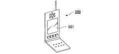
図16は、携帯電話の一例を示した斜視図である。図16において、500は携帯電話本体を示し、501は前記のダブルゲートTFTを備えた液晶装置(電気光学装置)の液晶表示部を示している。
図16に示す電子機器は、上記実施例のLDD構造のダブルゲートTFTを備えた液晶装置を有するものであるので、性能に優れたものとなる。[Electronics]
Next, specific examples of the electronic apparatus having the electro-optical device including the double gate TFT having the LDD structure according to the first to sixth embodiments of the present invention will be described.
FIG. 16 is a perspective view showing an example of a mobile phone. In FIG. 16,
The electronic device shown in FIG. 16 has a liquid crystal device including the double gate TFT of the LDD structure of the above embodiment, and thus has excellent performance.
10A 透光性を有する基板本体(透光性基板)
33 下部ゲート電極(第1のゲート電極)
34 下部ゲート絶縁膜(第1の絶縁膜)
35 半導体薄膜
35a チャネル領域
35b 低濃度ソース領域
35c 低濃度ドレイン領域
35d 高濃度ソース領域
35e 高濃度ドレイン領域
36 上部ゲート絶縁膜(第2の絶縁膜)
36a 第1絶縁層
36b 第2絶縁層
37 上部ゲート電極(第2のゲート電極)
38 層間絶縁膜
39 開口部
71 開口部
76 ポジ型フォトレジスト
76a 硬化領域
77 低濃度の不純物イオン
81 高濃度の不純物イオン
91 開口部
111 上部ゲート絶縁膜(第2の絶縁膜)
111a 中央部分
111b 周辺部分
112 ネガ型フォトレジスト
113 開口部
114 凹部
10A Translucent substrate body (translucent substrate)
33 Lower gate electrode (first gate electrode)
34 Lower gate insulating film (first insulating film)
35 Semiconductor
36a
38
111a
Claims (9)
Translated fromJapanese前記チャネル領域に、前記第1の絶縁膜を介して第1のゲート電極が対向配置されるとともに、前記第2の絶縁膜を介して第2のゲート電極が対向配置され、前記ソース領域及びドレイン領域には、それぞれ不純物濃度が相対的に高い高濃度領域と不純物濃度が相対的に低い低濃度領域とが形成されてなる薄膜半導体装置において、
前記第2の絶縁膜は、前記チャネル領域の中央部に対応する部分の厚みが、前記チャネル領域の前記ソース領域及びドレイン領域それぞれの近傍に対応する部分の厚みより薄いことを特徴とする薄膜半導体装置。A first insulating film, a channel region, a semiconductor thin film having a source region and a drain region, and a second insulating film are sequentially stacked;
A first gate electrode is disposed opposite to the channel region via the first insulating film, and a second gate electrode is disposed opposite to the channel region via the second insulating film. In the thin film semiconductor device in which a high concentration region having a relatively high impurity concentration and a low concentration region having a relatively low impurity concentration are formed in each region,
The thin film semiconductor, wherein the second insulating film has a thickness corresponding to a central portion of the channel region that is smaller than a thickness corresponding to the vicinity of each of the source region and the drain region of the channel region. apparatus.
前記第1の絶縁層の前記チャネル領域に対応する位置には、前記第1のゲート電極と同じ大きさの開口部が形成されていることを特徴とする請求項1記載の薄膜半導体装置。The second insulating film includes a first insulating layer formed on the semiconductor thin film, and a second insulating layer formed on the first insulating layer,
2. The thin film semiconductor device according to claim 1, wherein an opening having the same size as that of the first gate electrode is formed at a position corresponding to the channel region of the first insulating layer.
前記第1の絶縁層の前記チャネル領域に対応する位置には、前記第1のゲート電極より狭い開口部が形成されていることを特徴とする請求項1記載の薄膜半導体装置。The second insulating film includes a first insulating layer formed on the semiconductor thin film, and a second insulating layer formed on the first insulating layer,
2. The thin film semiconductor device according to claim 1, wherein an opening narrower than the first gate electrode is formed at a position corresponding to the channel region of the first insulating layer.
前記第1の絶縁層の前記チャネル領域に対応する位置には、前記第1のゲート電極より広い開口部が形成されていることを特徴とする請求項1記載の薄膜半導体装置。The second insulating film includes a first insulating layer formed on the semiconductor thin film, and a second insulating layer formed on the first insulating layer,
2. The thin film semiconductor device according to claim 1, wherein an opening wider than the first gate electrode is formed at a position corresponding to the channel region of the first insulating layer.
前記チャネル領域に、前記第1の絶縁膜を介して第1のゲート電極が対向配置されるとともに、前記第2の絶縁膜を介して第2のゲート電極が対向配置され、前記ソース領域及びドレイン領域には、それぞれ不純物濃度が相対的に高い高濃度領域と不純物濃度が相対的に低い低濃度領域とが形成されてなる薄膜半導体装置の製造方法であって、
透光性基板上に、遮光性を有する第1のゲート電極を形成する工程と、
前記第1のゲート電極を含む前記透光性基板上に、第1の絶縁膜、半導体薄膜を順次積層する工程と、
前記半導体薄膜上にポジ型フォトレジストを塗布する工程と、
前記透光性基板の裏面側から前記第1のゲート電極をマスクとして前記フォトレジストを露光し、所定形状にパターニングする工程と、
このパターニングされたフォトレジストをマスクとして前記半導体薄膜に低濃度の不純物を注入する工程と、
これらパターニングされたフォトレジスト及び半導体薄膜を含む第1の絶縁膜上に第1の絶縁層を成膜する工程と、
リフトオフ法により前記パターニングされたフォトレジストと該フォトレジスト上の前記第1の絶縁層を除去し、該第1の絶縁層の前記半導体薄膜のチャネル領域の中央部に対応する部分を開口部とする工程と、
残部の第1の絶縁層を含む前記半導体薄膜上に第2の絶縁層を形成する工程と、
この第2の絶縁層上に前記第1のゲート電極より幅広の第2のゲート電極を形成する工程と、
この第2のゲート電極をマスクとして、前記半導体薄膜に高濃度の不純物を注入する工程と、
を有することを特徴とする薄膜半導体装置の製造方法。A first insulating film, a channel region, a semiconductor thin film having a source region and a drain region, and a second insulating film composed of first and second insulating layers are sequentially stacked;
A first gate electrode is disposed opposite to the channel region via the first insulating film, and a second gate electrode is disposed opposite to the channel region via the second insulating film. Each of the regions is a method of manufacturing a thin film semiconductor device in which a high concentration region having a relatively high impurity concentration and a low concentration region having a relatively low impurity concentration are formed.
Forming a light-shielding first gate electrode on a light-transmitting substrate;
Sequentially stacking a first insulating film and a semiconductor thin film on the translucent substrate including the first gate electrode;
Applying a positive photoresist on the semiconductor thin film;
Exposing the photoresist from the back side of the translucent substrate using the first gate electrode as a mask, and patterning the photoresist into a predetermined shape;
Implanting low-concentration impurities into the semiconductor thin film using the patterned photoresist as a mask;
Forming a first insulating layer on the first insulating film including the patterned photoresist and semiconductor thin film; and
The patterned photoresist and the first insulating layer on the photoresist are removed by a lift-off method, and a portion corresponding to the central portion of the channel region of the semiconductor thin film of the first insulating layer is used as an opening. Process,
Forming a second insulating layer on the semiconductor thin film including the remaining first insulating layer;
Forming a second gate electrode wider than the first gate electrode on the second insulating layer;
Using the second gate electrode as a mask, implanting high-concentration impurities into the semiconductor thin film;
A method for manufacturing a thin film semiconductor device, comprising:
前記チャネル領域に、前記第1の絶縁膜を介して第1のゲート電極が対向配置されるとともに、前記第2の絶縁膜を介して第2のゲート電極が対向配置され、前記ソース領域及びドレイン領域には、それぞれ不純物濃度が相対的に高い高濃度領域と不純物濃度が相対的に低い低濃度領域とが形成されてなる薄膜半導体装置の製造方法であって、
透光性基板上に、遮光性を有する第1のゲート電極を形成する工程と、
前記第1のゲート電極を含む前記透光性基板上に、第1の絶縁膜、半導体薄膜を順次積層する工程と、
前記半導体薄膜上にポジ型フォトレジストを塗布する工程と、
前記透光性基板の裏面側から前記第1のゲート電極をマスクとして前記フォトレジストを露光し、所定形状にパターニングする工程と、
これらパターニングされたフォトレジスト及び半導体薄膜を含む第1の絶縁膜上に第1の絶縁層を成膜する工程と、
これらパターニングされたフォトレジスト及び第1の絶縁層をマスクとして前記半導体薄膜に低濃度の不純物を注入する工程と、
リフトオフ法により前記パターニングされたフォトレジストと該フォトレジスト上の前記第1の絶縁層を除去し、該第1の絶縁層の前記半導体薄膜のチャネル領域の中央部に対応する部分を開口部とする工程と、
残部の第1の絶縁層を含む前記半導体薄膜上に第2の絶縁層を形成する工程と、
この第2の絶縁層上に前記第1のゲート電極より幅広の第2のゲート電極を形成する工程と、
この第2のゲート電極をマスクとして、前記半導体薄膜に高濃度の不純物を注入する工程と、
を有することを特徴とする薄膜半導体装置の製造方法。A first insulating film, a channel region, a semiconductor thin film having a source region and a drain region, and a second insulating film composed of first and second insulating layers are sequentially stacked;
A first gate electrode is disposed opposite to the channel region via the first insulating film, and a second gate electrode is disposed opposite to the channel region via the second insulating film. Each of the regions is a method of manufacturing a thin film semiconductor device in which a high concentration region having a relatively high impurity concentration and a low concentration region having a relatively low impurity concentration are formed.
Forming a light-shielding first gate electrode on a light-transmitting substrate;
Sequentially stacking a first insulating film and a semiconductor thin film on the translucent substrate including the first gate electrode;
Applying a positive photoresist on the semiconductor thin film;
Exposing the photoresist from the back side of the translucent substrate using the first gate electrode as a mask, and patterning the photoresist into a predetermined shape;
Forming a first insulating layer on the first insulating film including the patterned photoresist and semiconductor thin film; and
Implanting low-concentration impurities into the semiconductor thin film using the patterned photoresist and the first insulating layer as a mask;
The patterned photoresist and the first insulating layer on the photoresist are removed by a lift-off method, and a portion corresponding to the central portion of the channel region of the semiconductor thin film of the first insulating layer is used as an opening. Process,
Forming a second insulating layer on the semiconductor thin film including the remaining first insulating layer;
Forming a second gate electrode wider than the first gate electrode on the second insulating layer;
Using the second gate electrode as a mask, implanting high-concentration impurities into the semiconductor thin film;
A method for manufacturing a thin film semiconductor device, comprising:
前記チャネル領域に、前記第1の絶縁膜を介して第1のゲート電極が対向配置されるとともに、前記第2の絶縁膜を介して第2のゲート電極が対向配置され、前記ソース領域及びドレイン領域には、それぞれ不純物濃度が相対的に高い高濃度領域と不純物濃度が相対的に低い低濃度領域とが形成されてなる薄膜半導体装置の製造方法であって、
透光性基板上に、遮光性を有する第1のゲート電極を形成する工程と、
前記第1のゲート電極を含む前記透光性基板上に、第1の絶縁膜、半導体薄膜を順次積層する工程と、
前記半導体薄膜上にポジ型フォトレジストを塗布する工程と、
前記透光性基板の裏面側から前記第1のゲート電極をマスクとして前記ポジ型フォトレジストを露光し、所定形状にパターニングする工程と、
このパターニングされたポジ型フォトレジストをマスクとして前記半導体薄膜に低濃度の不純物を注入する工程と、
これらパターニングされたフォトレジスト及び半導体薄膜を含む第1の絶縁膜上に第2の絶縁膜を成膜する工程と、
前記第2の絶縁膜上にネガ型フォトレジストを塗布する工程と、
前記透光性基板の裏面側から前記第1のゲート電極をマスクとして前記ネガ型フォトレジストを露光し、所定形状にパターニングする工程と、
このパターニングされたネガ型フォトレジストをマスクとして前記第2の絶縁膜を選択除去し、該第2の絶縁膜の前記半導体薄膜のチャネル領域の中央部に対応する部分の厚みを、この部分以外の厚みより薄くする工程と、
前記ネガ型フォトレジストを除去し、前記第2の絶縁膜上に前記第1のゲート電極より幅広の第2のゲート電極を形成する工程と、
この第2のゲート電極をマスクとして、前記半導体薄膜に高濃度の不純物を注入する工程と、
を有することを特徴とする薄膜半導体装置の製造方法。A first insulating film, a channel region, a semiconductor thin film having a source region and a drain region, and a second insulating film are sequentially stacked;
A first gate electrode is disposed opposite to the channel region via the first insulating film, and a second gate electrode is disposed opposite to the channel region via the second insulating film. Each of the regions is a method of manufacturing a thin film semiconductor device in which a high concentration region having a relatively high impurity concentration and a low concentration region having a relatively low impurity concentration are formed.
Forming a light-shielding first gate electrode on a light-transmitting substrate;
Sequentially stacking a first insulating film and a semiconductor thin film on the translucent substrate including the first gate electrode;
Applying a positive photoresist on the semiconductor thin film;
Exposing the positive photoresist from the back side of the translucent substrate using the first gate electrode as a mask, and patterning it into a predetermined shape;
Implanting low-concentration impurities into the semiconductor thin film using the patterned positive photoresist as a mask;
Forming a second insulating film on the first insulating film including the patterned photoresist and semiconductor thin film; and
Applying a negative photoresist on the second insulating film;
Exposing the negative photoresist from the back side of the translucent substrate using the first gate electrode as a mask, and patterning the negative photoresist;
The second insulating film is selectively removed using the patterned negative photoresist as a mask, and the thickness of the portion of the second insulating film corresponding to the central portion of the channel region of the semiconductor thin film is set to a portion other than this portion. Making it thinner than the thickness;
Removing the negative photoresist and forming a second gate electrode wider than the first gate electrode on the second insulating film;
Using the second gate electrode as a mask, implanting high-concentration impurities into the semiconductor thin film;
A method for manufacturing a thin film semiconductor device, comprising:
Priority Applications (1)
| Application Number | Priority Date | Filing Date | Title |
|---|---|---|---|
| JP2003306802AJP2005079283A (en) | 2003-08-29 | 2003-08-29 | Thin film semiconductor device and manufacturing method thereof, electro-optical device, and electronic apparatus |
Applications Claiming Priority (1)
| Application Number | Priority Date | Filing Date | Title |
|---|---|---|---|
| JP2003306802AJP2005079283A (en) | 2003-08-29 | 2003-08-29 | Thin film semiconductor device and manufacturing method thereof, electro-optical device, and electronic apparatus |
Publications (1)
| Publication Number | Publication Date |
|---|---|
| JP2005079283Atrue JP2005079283A (en) | 2005-03-24 |
Family
ID=34409783
Family Applications (1)
| Application Number | Title | Priority Date | Filing Date |
|---|---|---|---|
| JP2003306802AWithdrawnJP2005079283A (en) | 2003-08-29 | 2003-08-29 | Thin film semiconductor device and manufacturing method thereof, electro-optical device, and electronic apparatus |
Country Status (1)
| Country | Link |
|---|---|
| JP (1) | JP2005079283A (en) |
Cited By (24)
| Publication number | Priority date | Publication date | Assignee | Title |
|---|---|---|---|---|
| JP2006278623A (en)* | 2005-03-29 | 2006-10-12 | Sanyo Epson Imaging Devices Corp | Thin film transistor, electro-optical device and electronic device |
| KR100647690B1 (en) | 2005-04-22 | 2006-11-23 | 삼성에스디아이 주식회사 | Thin film transistor and flat panel display device having same |
| JP2007273956A (en)* | 2006-03-31 | 2007-10-18 | Genta Kagi Kogyo Kofun Yugenkoshi | Thin film transistor array substrate and electronic ink display device |
| JP2008058850A (en)* | 2006-09-04 | 2008-03-13 | Mitsubishi Electric Corp | Display device and manufacturing method thereof |
| WO2009091176A3 (en)* | 2008-01-14 | 2009-11-05 | 서울대학교산학협력단 | Light emitting device using diode structure controlled by double gate, and semiconductor apparatus including the same |
| KR100971716B1 (en) | 2008-01-14 | 2010-07-21 | 서울대학교산학협력단 | Light emitting device using diode structure controlled by double gate |
| JP2011064805A (en)* | 2009-09-15 | 2011-03-31 | Toshiba Mobile Display Co Ltd | Liquid crystal display apparatus |
| US8012812B2 (en) | 2007-07-17 | 2011-09-06 | Semiconductor Energy Laboratory Co., Ltd. | Semiconductor device and method for manufacturing the same |
| CN102299178A (en)* | 2010-06-22 | 2011-12-28 | 中国科学院微电子研究所 | Semiconductor structure and preparation method thereof |
| US8493292B2 (en) | 2006-01-10 | 2013-07-23 | Samsung Display Co., Ltd. | Organic light emitting diode display and manufacturing method thereof |
| JP2013201435A (en)* | 2009-07-03 | 2013-10-03 | Semiconductor Energy Lab Co Ltd | Semiconductor device |
| KR101334177B1 (en) | 2007-02-15 | 2013-11-28 | 재단법인서울대학교산학협력재단 | Thin Film Transistor And Method for Manufacturing the Same |
| US8704219B2 (en) | 2010-03-26 | 2014-04-22 | Semiconductor Energy Laboratory Co., Ltd. | Method for manufacturing semiconductor device |
| KR101442800B1 (en) | 2008-09-02 | 2014-09-23 | 서울대학교산학협력단 | A semiconductor device comprising a dual gate controlled diode structure |
| GB2515750A (en)* | 2013-07-01 | 2015-01-07 | Plastic Logic Ltd | Supressing Leakage Currents in a Multi - TFT Device |
| JP2015041629A (en)* | 2013-08-20 | 2015-03-02 | ソニー株式会社 | Radiation imaging apparatus and radiation imaging display system |
| JP2015092620A (en)* | 2011-02-02 | 2015-05-14 | 株式会社半導体エネルギー研究所 | Semiconductor device |
| JP2016018759A (en)* | 2014-07-11 | 2016-02-01 | 株式会社ジャパンディスプレイ | Organic EL display device and manufacturing method thereof |
| US9349752B2 (en) | 2011-01-12 | 2016-05-24 | Semiconductor Energy Laboratory Co., Ltd. | Semiconductor device and manufacturing method thereof |
| CN106483726A (en)* | 2016-12-21 | 2017-03-08 | 昆山龙腾光电有限公司 | Thin-film transistor array base-plate and preparation method and display panels |
| KR20180000792A (en)* | 2016-06-23 | 2018-01-04 | 삼성디스플레이 주식회사 | Thin film transistor array panel and manufacturing method thereof |
| KR20190075424A (en)* | 2017-12-21 | 2019-07-01 | 엘지디스플레이 주식회사 | Dual gate thin film transistor and self light emitting display device including the same |
| KR20190112229A (en)* | 2018-03-22 | 2019-10-04 | 삼성디스플레이 주식회사 | Thin film transistor array panel |
| US20240085752A1 (en)* | 2022-09-09 | 2024-03-14 | Sharp Display Technology Corporation | Active matrix substrate and liquid crystal display device |
- 2003
- 2003-08-29JPJP2003306802Apatent/JP2005079283A/ennot_activeWithdrawn
Cited By (48)
| Publication number | Priority date | Publication date | Assignee | Title |
|---|---|---|---|---|
| JP2006278623A (en)* | 2005-03-29 | 2006-10-12 | Sanyo Epson Imaging Devices Corp | Thin film transistor, electro-optical device and electronic device |
| KR100647690B1 (en) | 2005-04-22 | 2006-11-23 | 삼성에스디아이 주식회사 | Thin film transistor and flat panel display device having same |
| US8493292B2 (en) | 2006-01-10 | 2013-07-23 | Samsung Display Co., Ltd. | Organic light emitting diode display and manufacturing method thereof |
| JP2007273956A (en)* | 2006-03-31 | 2007-10-18 | Genta Kagi Kogyo Kofun Yugenkoshi | Thin film transistor array substrate and electronic ink display device |
| JP2008058850A (en)* | 2006-09-04 | 2008-03-13 | Mitsubishi Electric Corp | Display device and manufacturing method thereof |
| KR101334177B1 (en) | 2007-02-15 | 2013-11-28 | 재단법인서울대학교산학협력재단 | Thin Film Transistor And Method for Manufacturing the Same |
| US8012812B2 (en) | 2007-07-17 | 2011-09-06 | Semiconductor Energy Laboratory Co., Ltd. | Semiconductor device and method for manufacturing the same |
| US8674360B2 (en) | 2007-07-17 | 2014-03-18 | Semiconductor Energy Laboratory Co., Ltd. | Semiconductor device having first gate electrode and second gate electrode |
| WO2009091176A3 (en)* | 2008-01-14 | 2009-11-05 | 서울대학교산학협력단 | Light emitting device using diode structure controlled by double gate, and semiconductor apparatus including the same |
| KR100971716B1 (en) | 2008-01-14 | 2010-07-21 | 서울대학교산학협력단 | Light emitting device using diode structure controlled by double gate |
| KR101442800B1 (en) | 2008-09-02 | 2014-09-23 | 서울대학교산학협력단 | A semiconductor device comprising a dual gate controlled diode structure |
| US10714503B2 (en) | 2009-07-03 | 2020-07-14 | Semiconductor Energy Laboratory Co., Ltd. | Display device including transistor and manufacturing method thereof |
| US11637130B2 (en) | 2009-07-03 | 2023-04-25 | Semiconductor Energy Laboratory Co., Ltd. | Display device including transistor and manufacturing method thereof |
| US12272698B2 (en) | 2009-07-03 | 2025-04-08 | Semiconductor Energy Laboratory Co., Ltd. | Semiconductor device comprising driver circuit |
| US9837441B2 (en) | 2009-07-03 | 2017-12-05 | Semiconductor Energy Laboratory Co., Ltd. | Display device including transistor and manufacturing method thereof |
| US8735884B2 (en) | 2009-07-03 | 2014-05-27 | Semiconductor Energy Laboratory Co., Ltd. | Semiconductor device including oxide semiconductor |
| JP2013201435A (en)* | 2009-07-03 | 2013-10-03 | Semiconductor Energy Lab Co Ltd | Semiconductor device |
| US11257847B2 (en) | 2009-07-03 | 2022-02-22 | Semiconductor Energy Laboratory Co., Ltd. | Display device including transistor and manufacturing method thereof |
| US9812465B2 (en) | 2009-07-03 | 2017-11-07 | Semiconductor Energy Laboratory Co., Ltd. | Display device including transistor and manufacturing method thereof |
| US10211231B2 (en) | 2009-07-03 | 2019-02-19 | Semiconductor Energy Laboratory Co., Ltd. | Display device including transistor and manufacturing method thereof |
| US11978741B2 (en) | 2009-07-03 | 2024-05-07 | Semiconductor Energy Laboratory Co., Ltd. | Display device including transistor and manufacturing method thereof |
| US9130046B2 (en) | 2009-07-03 | 2015-09-08 | Semiconductor Energy Laboratory Co., Ltd. | Display device including transistor and manufacturing method thereof |
| JP2011064805A (en)* | 2009-09-15 | 2011-03-31 | Toshiba Mobile Display Co Ltd | Liquid crystal display apparatus |
| US8704219B2 (en) | 2010-03-26 | 2014-04-22 | Semiconductor Energy Laboratory Co., Ltd. | Method for manufacturing semiconductor device |
| CN102299178A (en)* | 2010-06-22 | 2011-12-28 | 中国科学院微电子研究所 | Semiconductor structure and preparation method thereof |
| CN102299178B (en)* | 2010-06-22 | 2014-03-26 | 中国科学院微电子研究所 | Semiconductor structure and preparation method thereof |
| TWI570809B (en)* | 2011-01-12 | 2017-02-11 | 半導體能源研究所股份有限公司 | Semiconductor device and method of manufacturing same |
| US9349752B2 (en) | 2011-01-12 | 2016-05-24 | Semiconductor Energy Laboratory Co., Ltd. | Semiconductor device and manufacturing method thereof |
| US9882062B2 (en) | 2011-01-12 | 2018-01-30 | Semiconductor Energy Laboratory Co., Ltd. | Semiconductor device and manufacturing method thereof |
| US9799773B2 (en) | 2011-02-02 | 2017-10-24 | Semiconductor Energy Laboratory Co., Ltd. | Transistor and semiconductor device |
| JP2015092620A (en)* | 2011-02-02 | 2015-05-14 | 株式会社半導体エネルギー研究所 | Semiconductor device |
| GB2515750B (en)* | 2013-07-01 | 2017-11-15 | Flexenable Ltd | Supressing Leakage Currents in a Multi - TFT Device |
| GB2515750A (en)* | 2013-07-01 | 2015-01-07 | Plastic Logic Ltd | Supressing Leakage Currents in a Multi - TFT Device |
| CN104425530A (en)* | 2013-08-20 | 2015-03-18 | 索尼公司 | Radiation image-pickup device and radiation image-pickup display system |
| JP2015041629A (en)* | 2013-08-20 | 2015-03-02 | ソニー株式会社 | Radiation imaging apparatus and radiation imaging display system |
| JP2016018759A (en)* | 2014-07-11 | 2016-02-01 | 株式会社ジャパンディスプレイ | Organic EL display device and manufacturing method thereof |
| KR20180000792A (en)* | 2016-06-23 | 2018-01-04 | 삼성디스플레이 주식회사 | Thin film transistor array panel and manufacturing method thereof |
| CN107546231B (en)* | 2016-06-23 | 2023-08-04 | 三星显示有限公司 | Thin Film Transistor Array Panel |
| KR102660292B1 (en)* | 2016-06-23 | 2024-04-24 | 삼성디스플레이 주식회사 | Thin film transistor array panel and manufacturing method thereof |
| CN107546231A (en)* | 2016-06-23 | 2018-01-05 | 三星显示有限公司 | Thin-film transistor display panel |
| CN106483726A (en)* | 2016-12-21 | 2017-03-08 | 昆山龙腾光电有限公司 | Thin-film transistor array base-plate and preparation method and display panels |
| KR20190075424A (en)* | 2017-12-21 | 2019-07-01 | 엘지디스플레이 주식회사 | Dual gate thin film transistor and self light emitting display device including the same |
| KR102532088B1 (en) | 2017-12-21 | 2023-05-12 | 엘지디스플레이 주식회사 | Dual gate thin film transistor and self light emitting display device including the same |
| KR20190112229A (en)* | 2018-03-22 | 2019-10-04 | 삼성디스플레이 주식회사 | Thin film transistor array panel |
| KR102579829B1 (en)* | 2018-03-22 | 2023-09-18 | 삼성디스플레이 주식회사 | Thin film transistor array panel |
| US12057509B2 (en) | 2018-03-22 | 2024-08-06 | Samsung Display Co., Ltd. | Thin film transistor array panel |
| US20240085752A1 (en)* | 2022-09-09 | 2024-03-14 | Sharp Display Technology Corporation | Active matrix substrate and liquid crystal display device |
| US12078903B2 (en) | 2022-09-09 | 2024-09-03 | Sharp Display Technology Corporation | Active matrix substrate and liquid crystal display device |
Similar Documents
| Publication | Publication Date | Title |
|---|---|---|
| JP2005079283A (en) | Thin film semiconductor device and manufacturing method thereof, electro-optical device, and electronic apparatus | |
| JP5111867B2 (en) | Display device | |
| JP4179393B2 (en) | Display device and manufacturing method thereof | |
| TWI401802B (en) | Thin film transistor plate and method of manufacturing same | |
| CN1873989B (en) | Thin film transistor and method of fabricating thin film transistor substrate | |
| US10361229B2 (en) | Display device | |
| KR100831881B1 (en) | Thin-film semiconductor device | |
| JP2009099887A (en) | Display device | |
| CN101853883B (en) | Thin film transistor, manufacturing method thereof, liquid crystal display panel and electronic device using same | |
| JP2005072144A (en) | Thin film semiconductor device and manufacturing method thereof, electro-optical device, and electronic apparatus | |
| JPH08250742A (en) | Semiconductor device | |
| JP2005072126A (en) | Circuit board, array substrate, manufacturing method therefor, liquid crystal display device and manufacturing method therefor | |
| US6847414B2 (en) | Manufacturing method for liquid crystal display | |
| KR20170077383A (en) | Substrate for display and display including the same | |
| JP2009130016A (en) | Semiconductor device manufacturing method and electronic apparatus | |
| JPH1065177A (en) | Thin film transistor device, method of manufacturing thin film transistor device, and liquid crystal display device | |
| JP4305192B2 (en) | Thin film semiconductor device manufacturing method, electro-optical device manufacturing method | |
| JP3536518B2 (en) | Polycrystalline semiconductor TFT, manufacturing method thereof, and TFT substrate | |
| JP2005033009A (en) | Thin-film semiconductor device manufacturing method, thin-film semiconductor device, electro-optical device manufacturing method, electro-optical device, and electronic apparatus | |
| JP2009272534A (en) | Semiconductor device, display and integrated circuit | |
| JP3966024B2 (en) | Thin film semiconductor device manufacturing method and electro-optical device manufacturing method | |
| JP2009210681A (en) | Display and manufacturing method therefor | |
| JP2010114160A (en) | Semiconductor element, method of manufacturing the same, and display device | |
| KR20070072208A (en) | Liquid Crystal Display Using Polysilicon Thin Film Transistor and Manufacturing Method Thereof | |
| KR20030096674A (en) | a thin film transistor array panel of using poly silicon and a method for manufacturing the same |
Legal Events
| Date | Code | Title | Description |
|---|---|---|---|
| A300 | Application deemed to be withdrawn because no request for examination was validly filed | Free format text:JAPANESE INTERMEDIATE CODE: A300 Effective date:20061107 |