JP2005069852A - Capacitive mechanical quantity sensor - Google Patents
Capacitive mechanical quantity sensorDownload PDFInfo
- Publication number
- JP2005069852A JP2005069852AJP2003299517AJP2003299517AJP2005069852AJP 2005069852 AJP2005069852 AJP 2005069852AJP 2003299517 AJP2003299517 AJP 2003299517AJP 2003299517 AJP2003299517 AJP 2003299517AJP 2005069852 AJP2005069852 AJP 2005069852A
- Authority
- JP
- Japan
- Prior art keywords
- fixed electrode
- mechanical quantity
- electrode
- quantity sensor
- substrate
- Prior art date
- Legal status (The legal status is an assumption and is not a legal conclusion. Google has not performed a legal analysis and makes no representation as to the accuracy of the status listed.)
- Withdrawn
Links
Images


Classifications
- G—PHYSICS
- G01—MEASURING; TESTING
- G01C—MEASURING DISTANCES, LEVELS OR BEARINGS; SURVEYING; NAVIGATION; GYROSCOPIC INSTRUMENTS; PHOTOGRAMMETRY OR VIDEOGRAMMETRY
- G01C19/00—Gyroscopes; Turn-sensitive devices using vibrating masses; Turn-sensitive devices without moving masses; Measuring angular rate using gyroscopic effects
- G01C19/56—Turn-sensitive devices using vibrating masses, e.g. vibratory angular rate sensors based on Coriolis forces
- G01C19/5719—Turn-sensitive devices using vibrating masses, e.g. vibratory angular rate sensors based on Coriolis forces using planar vibrating masses driven in a translation vibration along an axis
- G—PHYSICS
- G01—MEASURING; TESTING
- G01P—MEASURING LINEAR OR ANGULAR SPEED, ACCELERATION, DECELERATION, OR SHOCK; INDICATING PRESENCE, ABSENCE, OR DIRECTION, OF MOVEMENT
- G01P15/00—Measuring acceleration; Measuring deceleration; Measuring shock, i.e. sudden change of acceleration
- G01P15/02—Measuring acceleration; Measuring deceleration; Measuring shock, i.e. sudden change of acceleration by making use of inertia forces using solid seismic masses
- G01P15/08—Measuring acceleration; Measuring deceleration; Measuring shock, i.e. sudden change of acceleration by making use of inertia forces using solid seismic masses with conversion into electric or magnetic values
- G01P15/125—Measuring acceleration; Measuring deceleration; Measuring shock, i.e. sudden change of acceleration by making use of inertia forces using solid seismic masses with conversion into electric or magnetic values by capacitive pick-up
- H—ELECTRICITY
- H10—SEMICONDUCTOR DEVICES; ELECTRIC SOLID-STATE DEVICES NOT OTHERWISE PROVIDED FOR
- H10D—INORGANIC ELECTRIC SEMICONDUCTOR DEVICES
- H10D48/00—Individual devices not covered by groups H10D1/00 - H10D44/00
- H10D48/50—Devices controlled by mechanical forces, e.g. pressure
- G—PHYSICS
- G01—MEASURING; TESTING
- G01P—MEASURING LINEAR OR ANGULAR SPEED, ACCELERATION, DECELERATION, OR SHOCK; INDICATING PRESENCE, ABSENCE, OR DIRECTION, OF MOVEMENT
- G01P15/00—Measuring acceleration; Measuring deceleration; Measuring shock, i.e. sudden change of acceleration
- G01P15/02—Measuring acceleration; Measuring deceleration; Measuring shock, i.e. sudden change of acceleration by making use of inertia forces using solid seismic masses
- G01P15/08—Measuring acceleration; Measuring deceleration; Measuring shock, i.e. sudden change of acceleration by making use of inertia forces using solid seismic masses with conversion into electric or magnetic values
- G01P2015/0805—Measuring acceleration; Measuring deceleration; Measuring shock, i.e. sudden change of acceleration by making use of inertia forces using solid seismic masses with conversion into electric or magnetic values being provided with a particular type of spring-mass-system for defining the displacement of a seismic mass due to an external acceleration
- G01P2015/0822—Measuring acceleration; Measuring deceleration; Measuring shock, i.e. sudden change of acceleration by making use of inertia forces using solid seismic masses with conversion into electric or magnetic values being provided with a particular type of spring-mass-system for defining the displacement of a seismic mass due to an external acceleration for defining out-of-plane movement of the mass
- G01P2015/084—Measuring acceleration; Measuring deceleration; Measuring shock, i.e. sudden change of acceleration by making use of inertia forces using solid seismic masses with conversion into electric or magnetic values being provided with a particular type of spring-mass-system for defining the displacement of a seismic mass due to an external acceleration for defining out-of-plane movement of the mass the mass being suspended at more than one of its sides, e.g. membrane-type suspension, so as to permit multi-axis movement of the mass
Landscapes
- Physics & Mathematics (AREA)
- General Physics & Mathematics (AREA)
- Engineering & Computer Science (AREA)
- Radar, Positioning & Navigation (AREA)
- Remote Sensing (AREA)
- Gyroscopes (AREA)
- Pressure Sensors (AREA)
Abstract
Translated fromJapaneseDescription
Translated fromJapaneseこの発明は、加速度、角速度といった力学的物理量を検出する装置に関する。特に、半導体プロセスを用いて製造する構造体が変位することによる容量変化を検出することにより力学的物理量を検出する容量型力学量センサに関する。 The present invention relates to an apparatus for detecting mechanical physical quantities such as acceleration and angular velocity. In particular, the present invention relates to a capacitive mechanical quantity sensor that detects a mechanical physical quantity by detecting a change in capacity caused by displacement of a structure manufactured using a semiconductor process.
従来、外部から加わる加速度や角速度により変位する錘やその錘を支持する梁を半導体基板内に形成し、錘の可動電極に対し微小間隔を隔てて形成された固定電極との静電容量変化を検出する静電容量型力学量センサが知られている(例えば、特許文献1参照))。図7にその概略図を示す。このセンサでは、錘71と梁72を微細加工で半導体基板73内に作製し、両面から上側基板74、下側基板75で接合し封止している。こうした静電容量型のセンサは、微小隙間76,77に対し、センサ感度が敏感であり、微小隙間ばらつきがセンサ感度特性に大きく影響する。微小隙間76、77は、上側基板74と下側基板75、或いは半導体基板73をエッチングすることにより形成したギャップと、上側基盤74と下側基板75の、半導体基板73と対向する面に形成する固定電極78の厚みにより決定される。従って、固定電極の厚み制御は重要である。例えば、固定電極上にヒロックが発生した場合、微小隙間76,77のばらつきを生じさせる他に、錘の可動範囲を狭め、感度低下を招く。
しかしながら、特開平8-94666の方法によれば、
上側基板と下側基板に硝子基板を使用しており、硝子基板上に形成する固定電極からヒロックが発生することを回避する方法として、Tiを下地層としてAlとの2層電極構造を採用している。しかし、多層電極とすることにより製造コストが大きくなる。さらに、異種電極間の熱膨張差により電極の膜剥がれを引き起こし易くなり、信頼性が低下する。さらに、Tiの抵抗値が高い為、Alの厚みを厚くして抵抗値の低減を図る必要があり、トータルの電極厚みが厚くなることから、電極厚みのばらつきが発生しやすくなる。However, according to the method of JP-A-8-94666,
A glass substrate is used for the upper substrate and the lower substrate, and as a method of avoiding hillocks from the fixed electrode formed on the glass substrate, a two-layer electrode structure of Ti with Ti as an underlayer is adopted. ing. However, the production cost increases by using a multilayer electrode. Further, the difference in thermal expansion between different types of electrodes tends to cause peeling of the electrode film, resulting in a decrease in reliability. Furthermore, since the resistance value of Ti is high, it is necessary to increase the thickness of Al to reduce the resistance value. Since the total electrode thickness is increased, variations in the electrode thickness are likely to occur.
本発明は、上記の問題に鑑みてなされたものであり、加速度、角速度といった力学的物理量を、半導体プロセスを用いて製造する構造体が変位することによる容量変化を検出する容量型力学量センサにおいて、
梁により支持され、外部より印加される加速度や角速度といった力学量により変位する錘を有する半導体基板と、半導体基板の表面の一部と接合し、錘の対向する位置に微小隙間1を隔てて配置した固定電極1を積層させた、上部基板と、半導体基板の裏面の一部と接合し、錘の対向する位置に微小隙間2を隔てて配置した固定電極2を積層させた、下部基板とから成り、錘の変位による固定電極1及び固定電極2の容量変化から力学量を測定する容量型力学量センサにおいて、固定電極1の一部、若しくは固定電極2の一部に、複数の溝、若しくは複数の穴を形成する。
また、前記複数の溝、若しくは前記複数の穴が等間隔に配置されていることを特徴としている。
また、固定電極1、若しくは固定電極2が、単一金属で形成されることを特徴としている。The present invention has been made in view of the above problems, and is a capacitive mechanical quantity sensor that detects a change in capacitance caused by displacement of a structure manufactured using a semiconductor process, such as a mechanical physical quantity such as acceleration and angular velocity. ,
A semiconductor substrate having a weight supported by a beam and displaced by a mechanical quantity such as acceleration or angular velocity applied from the outside, and a part of the surface of the semiconductor substrate are joined, and a
Further, the plurality of grooves or the plurality of holes are arranged at equal intervals.
Further, the
従って、固定電極が単一材料であってもヒロックを回避でき、膜剥がれ等の信頼性も向上できる。また、Al等低コストの材料が採用でき、電極厚みばらつきの改善とともに、製造コスト・歩留まりの改善も見込める。 Therefore, even if the fixed electrode is a single material, hillocks can be avoided and the reliability such as film peeling can be improved. In addition, low-cost materials such as Al can be used, which can improve the manufacturing cost and yield as well as the variation in electrode thickness.
静電容量型力学量センサにおいて、上下基板表面の金属電極に溝や穴のパターンを一定間隔で形成することにより、単一電極においても電極上のヒロック回避が可能となる為、膜剥がれの心配が少ない信頼性の高い力学量センサを低価格で供給できる。 Capacitance-type mechanical quantity sensors can prevent hillocks on the electrode even if a single electrode is formed by forming grooves and holes in the metal electrodes on the upper and lower substrate surfaces at regular intervals. Highly reliable mechanical quantity sensors with low cost can be supplied at a low price.
以下、本発明の力学量センサを代表して角速度センサを例にあげ、添付の図面を参照して詳細に説明する。 Hereinafter, an angular velocity sensor will be taken as an example of the mechanical quantity sensor of the present invention and will be described in detail with reference to the accompanying drawings.
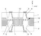
まず、図1に、本発明の実施の形態1に係わる角速度センサの断面図を図1に示す。本力学量センサは、上部硝子基板1、シリコン基板2、下部硝子基板3の3層構造をしており、それら3基板を接合して構造体を作製する。シリコン基板2内には、エッチングにより梁4と錘5を有した振動体が形成されており、外部より加わる力により、振動させたり、捩れる動きが可能となる。梁4の厚み、長さ、幅及び、錘5の厚み、面積等の形状は、任意の共振周波数及びバネ定数が得られるよう設計される。また、シリコン基板2の梁4及び錘5と、それぞれ対向する硝子との間には、微小隙間6、7が存在する。振動体を形成したシリコン基板2を上下より挟み込む上側硝子基板1と下側硝子基板3の一部には、貫通穴8が形成され、これら貫通穴8を通して、硝子内側に形成した電極を外側に引き出す構造をしている。貫通穴8の外側には、導電性材料9が積層されており、硝子内の封止は維持される。硝子基板の内側に形成された固定電極は、貫通穴8の側壁に形成した配線を通し、この導電性材料9から外へ取り出している。 First, FIG. 1 shows a sectional view of an angular velocity sensor according to
本角速度センサは、シリコン基板2の電位を制御する必要があるが、硝子内面に形成する電極の一部をシリコン基板2に形成した基板電極12と接触させることにより、シリコン基板2の電位を確保する。ここで、本角速度センサの動作原理を以下簡単に説明する。上側硝子基板1と下側硝子基板3の内面側に設けた励起用固定電極10に交流電圧を印加させ、グランドに保持した振動体(可動電極)との間に働く静電力により錘を上下振動させる。このようにz軸方向に速度が与えられた振動体に、y軸周りの角速度が加わると、x軸方向にそれらの積のコリオリ力が与えられ、図2に示すように、梁が撓む。上側硝子基板1と下側硝子基板3の内面側には、検出用固定電極11を設けてあり、梁の撓みによる錘の傾きから、検出用固定電極11と可動電極の容量に変化が生じ、この容量変化から角速度の大きさを検出する。 Although this angular velocity sensor needs to control the potential of the
このように、容量検出型の角速度センサでは、固定電極と可動電極との距離が直接容量の大きさに係わる為、その距離にばらつきがあると、励起用固定電極10と可動電極との間に働く静電力が変化し上下振動の速度がばらつくと共に、検出用固定電極11と可動電極間の容量もばらつき、検出感度へ大きく影響する。また、励起用固定電極10上、若しくは検出用固定電極11上にヒロックが発生すると、微小隙間6、7のばらつきによる検出感度ばらつきが発生するとともに、錘の可動範囲が狭まり、センサの感度低下を招く。一般に、金や白金を使用することにより、ヒロックを回避でき、抵抗値も低く設定できるが、高価な材料であり、製造コストが増加する。また、これらの金属は、硝子との密着力が弱いため、硝子との間に密着を強化する膜を積層する必要があり、多層構造が強いられる。多層構造は、膜剥がれの原因となる為、信頼性の面で劣る。 As described above, in the capacitance detection type angular velocity sensor, the distance between the fixed electrode and the movable electrode is directly related to the size of the capacitance. Therefore, if the distance varies, the distance between the excitation fixed
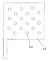
図3は、本実施の形態1に係わる角速度センサの固定電極(励起用固定電極10、検出用固定電極11)を説明した図である。固定電極31には、丸形状の穴32が等間隔に規則的に形成されている。例えば、穴32が無いような固定電極に、Al等低エネルギーで移動が容易な材料を使用した場合、熱工程により表面にヒロックが発生しやすい。しかし、図3のように穴32が形成されている場合、Alのエネルギーが穴の側面方向に分散され、表面にはヒロックが発生しにくくなる。穴32の間隔は、任意に設定でき、プロセス(特に熱工程)に適した間隔により、表面へのヒロック発生を阻止できる。この穴32の形状は、丸に限らず、多角形であっても勿論良い。 FIG. 3 is a diagram illustrating the fixed electrodes (excitation
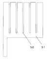
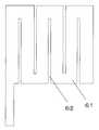
また、図4に示すように、溝42を等間隔に配置しても同様の効果を得ることは可能である。この溝42は、長方形に限らす、多角形や楕円であっても構わない。またその長辺及び長軸の方向も図示する方向に限ったものでは無い。また、図5及び図6のように、溝の一辺が固定電極の外周に接した構造であっても良く、つまり、電極が電位的に繋がれている構造であれば構わない。このような図3から図6に示した電極の形状は、電極形成時のフォトマスクに書き込むことにより、一般の半導体プロセス同様、容易に作製できる。また、Al等材料費が安く、抵抗値の低い材料により作製でき、低コスト化に対応できる。また単一膜で固定電極を形成でき、膜剥がれを起こし難く、信頼性に優れたデバイスが作製できる。 As shown in FIG. 4, the same effect can be obtained even if the
このような例は、角速度センサに限らず、加速度センサや圧力センサ等の容量変化検出型の力学量センサ全般に当てはまる。 Such an example applies not only to the angular velocity sensor but also to general capacitance change detection type mechanical quantity sensors such as an acceleration sensor and a pressure sensor.
小型化・低コスト化に適した、本発明の実施の形態1に係る静電容量型力学量センサは、主に、携帯・ハンディ機器や、バーチャルリアリティ等における、運動をモニタリングする機能で使用されることが予想される。例えば、重力を利用して傾き角の情報を検知するセンサや、カメラ等における手ぶれを補正する為に用いるセンサとして有効であり、低コスト・小型というメリットから民生用として多くに活用されると考えられる。 The capacitance type mechanical quantity sensor according to the first embodiment of the present invention, which is suitable for downsizing and cost reduction, is mainly used for the function of monitoring movement in portable / handy devices, virtual reality, and the like. Is expected. For example, it is effective as a sensor for detecting tilt angle information using gravity and a sensor used to correct camera shake in cameras, etc., and is considered to be widely used for consumer use due to its low cost and small size. It is done.
1 上部硝子基板
2 シリコン基板
3 下部硝子基板
4 梁
5 錘
6、7 微小隙間
8 貫通穴
9 導電性材料
10 励起用固定電極
11 検出用固定電極
12 基板電極
31、41、51、61 固定電極
32 穴
42、52、62 溝
71 錘
72 梁
73 半導体基板
74 上側基板
75 下側基板
76、77 微小隙間
78 固定電極DESCRIPTION OF
Claims (3)
Translated fromJapanese前記半導体基板の表面の一部と接合し、前記錘の対向する位置に微小隙間1を隔てて配置した固定電極1を積層させた、上部基板と、
前記半導体基板の裏面の一部と接合し、前記錘の対向する位置に微小隙間2を隔てて配置した固定電極2を積層させた、下部基板とから成り、
前記錘の変位による、前記固定電極1及び前記固定電極2の容量変化から前記力学量を測定する容量型力学量センサにおいて、
前記固定電極1の一部、若しくは前記固定電極2の一部に、複数の溝、若しくは複数の穴を形成することを特徴とする容量型力学量センサ。A semiconductor substrate having a weight supported by a beam and displaced by a mechanical quantity such as acceleration or angular velocity applied from the outside;
An upper substrate formed by laminating a fixed electrode 1 bonded to a part of the surface of the semiconductor substrate and arranged with a minute gap 1 at a position opposed to the weight;
A lower substrate formed by laminating a fixed electrode 2 bonded to a part of the back surface of the semiconductor substrate and arranged with a minute gap 2 at a position opposed to the weight;
In a capacitive mechanical quantity sensor that measures the mechanical quantity from the capacitance change of the fixed electrode 1 and the fixed electrode 2 due to displacement of the weight,
A capacitive mechanical quantity sensor, wherein a plurality of grooves or a plurality of holes are formed in a part of the fixed electrode 1 or a part of the fixed electrode 2.
Priority Applications (5)
| Application Number | Priority Date | Filing Date | Title |
|---|---|---|---|
| JP2003299517AJP2005069852A (en) | 2003-08-25 | 2003-08-25 | Capacitive mechanical quantity sensor |
| US10/920,017US7225675B2 (en) | 2003-08-25 | 2004-08-17 | Capacitance type dynamic quantity sensor |
| TW093124698ATW200522374A (en) | 2003-08-25 | 2004-08-17 | Capacitance type dynamic quantity sensor |
| KR1020040066793AKR20050022368A (en) | 2003-08-25 | 2004-08-24 | Capacitance type dynamic quantity sensor |
| CN200410068230ACN100580956C (en) | 2003-08-25 | 2004-08-25 | Capacitive Dynamic Quantity Sensor |
Applications Claiming Priority (1)
| Application Number | Priority Date | Filing Date | Title |
|---|---|---|---|
| JP2003299517AJP2005069852A (en) | 2003-08-25 | 2003-08-25 | Capacitive mechanical quantity sensor |
Publications (1)
| Publication Number | Publication Date |
|---|---|
| JP2005069852Atrue JP2005069852A (en) | 2005-03-17 |
Family
ID=34372410
Family Applications (1)
| Application Number | Title | Priority Date | Filing Date |
|---|---|---|---|
| JP2003299517AWithdrawnJP2005069852A (en) | 2003-08-25 | 2003-08-25 | Capacitive mechanical quantity sensor |
Country Status (5)
| Country | Link |
|---|---|
| US (1) | US7225675B2 (en) |
| JP (1) | JP2005069852A (en) |
| KR (1) | KR20050022368A (en) |
| CN (1) | CN100580956C (en) |
| TW (1) | TW200522374A (en) |
Cited By (4)
| Publication number | Priority date | Publication date | Assignee | Title |
|---|---|---|---|---|
| JP2006226989A (en)* | 2005-01-18 | 2006-08-31 | Denso Corp | Manufacturing method for pressure sensor |
| JP2008256598A (en)* | 2007-04-06 | 2008-10-23 | Denso Corp | Semiconductor dynamic quantity sensor |
| JP2010536036A (en)* | 2007-08-03 | 2010-11-25 | フリースケール セミコンダクター インコーポレイテッド | Symmetric differential capacitance sensor and manufacturing method thereof |
| JP2013217823A (en)* | 2012-04-11 | 2013-10-24 | Seiko Epson Corp | Physical quantity sensor and electronic apparatus |
Families Citing this family (8)
| Publication number | Priority date | Publication date | Assignee | Title |
|---|---|---|---|---|
| DE102008040368A1 (en)* | 2008-07-11 | 2010-02-18 | Airbus Deutschland Gmbh | Method for detecting a detachment of a stiffening component |
| DE102008043790B4 (en)* | 2008-11-17 | 2017-04-06 | Robert Bosch Gmbh | Micromechanical component |
| DE102008043788A1 (en)* | 2008-11-17 | 2010-05-20 | Robert Bosch Gmbh | Micromechanical component |
| CN102275860B (en)* | 2010-06-11 | 2014-12-31 | 张家港丽恒光微电子科技有限公司 | Manufacturing method of inertia micro-electro-mechanical sensor |
| JP6655281B2 (en)* | 2014-08-19 | 2020-02-26 | セイコーエプソン株式会社 | Physical quantity sensors, electronic devices and moving objects |
| US11268976B2 (en)* | 2017-02-23 | 2022-03-08 | Invensense, Inc. | Electrode layer partitioning |
| JP6691882B2 (en)* | 2017-03-03 | 2020-05-13 | 株式会社日立製作所 | Acceleration sensor |
| JP7238954B2 (en)* | 2021-01-13 | 2023-03-14 | 株式会社村田製作所 | MEMS device with meandering electrodes |
Family Cites Families (6)
| Publication number | Priority date | Publication date | Assignee | Title |
|---|---|---|---|---|
| US5228341A (en)* | 1989-10-18 | 1993-07-20 | Hitachi, Ltd. | Capacitive acceleration detector having reduced mass portion |
| EP0459723B1 (en)* | 1990-05-30 | 1996-01-17 | Hitachi, Ltd. | Semiconductor acceleration sensor and vehicle control system using the same |
| JP2728807B2 (en)* | 1991-07-24 | 1998-03-18 | 株式会社日立製作所 | Capacitive acceleration sensor |
| US5456111A (en)* | 1994-01-24 | 1995-10-10 | Alliedsignal Inc. | Capacitive drive vibrating beam accelerometer |
| US6035714A (en)* | 1997-09-08 | 2000-03-14 | The Regents Of The University Of Michigan | Microelectromechanical capacitive accelerometer and method of making same |
| US6105427A (en)* | 1998-07-31 | 2000-08-22 | Litton Systems, Inc. | Micro-mechanical semiconductor accelerometer |
- 2003
- 2003-08-25JPJP2003299517Apatent/JP2005069852A/ennot_activeWithdrawn
- 2004
- 2004-08-17USUS10/920,017patent/US7225675B2/ennot_activeExpired - Lifetime
- 2004-08-17TWTW093124698Apatent/TW200522374A/enunknown
- 2004-08-24KRKR1020040066793Apatent/KR20050022368A/ennot_activeCeased
- 2004-08-25CNCN200410068230Apatent/CN100580956C/ennot_activeExpired - Fee Related
Cited By (4)
| Publication number | Priority date | Publication date | Assignee | Title |
|---|---|---|---|---|
| JP2006226989A (en)* | 2005-01-18 | 2006-08-31 | Denso Corp | Manufacturing method for pressure sensor |
| JP2008256598A (en)* | 2007-04-06 | 2008-10-23 | Denso Corp | Semiconductor dynamic quantity sensor |
| JP2010536036A (en)* | 2007-08-03 | 2010-11-25 | フリースケール セミコンダクター インコーポレイテッド | Symmetric differential capacitance sensor and manufacturing method thereof |
| JP2013217823A (en)* | 2012-04-11 | 2013-10-24 | Seiko Epson Corp | Physical quantity sensor and electronic apparatus |
Also Published As
| Publication number | Publication date |
|---|---|
| KR20050022368A (en) | 2005-03-07 |
| CN100580956C (en) | 2010-01-13 |
| CN1591907A (en) | 2005-03-09 |
| US20050066729A1 (en) | 2005-03-31 |
| TW200522374A (en) | 2005-07-01 |
| US7225675B2 (en) | 2007-06-05 |
Similar Documents
| Publication | Publication Date | Title |
|---|---|---|
| US9831803B2 (en) | Membrane-based nano-electromechanical systems device and methods to make and use same | |
| CN110058051B (en) | Z-axis micro-electromechanical detection structure with drift reduction function | |
| JP5301767B2 (en) | Inertial sensor | |
| JP5450451B2 (en) | XY Axis Dual Mass Tuning Fork Gyroscope with Vertically Integrated Electronic Circuits and Wafer Scale Sealed Packaging | |
| CN103528578B (en) | Mems | |
| JP2010078500A (en) | Inertial sensor | |
| JP2005069852A (en) | Capacitive mechanical quantity sensor | |
| US20120125103A1 (en) | Z-axis capacitive accelerometer | |
| WO2013094208A1 (en) | Vibration-type angular velocity sensor | |
| US10371711B2 (en) | Damped linear accerelometer | |
| JP4555612B2 (en) | Capacitive mechanical quantity sensor | |
| US11112246B2 (en) | Torsional oscillator micro electro mechanical systems accelerometer | |
| CN106441260A (en) | On-silicon piezoelectric film multi-supporting-beam MEMS gyroscope and preparation method thereof | |
| JP4913467B2 (en) | Potential sensor | |
| JP4628018B2 (en) | Capacitive mechanical quantity sensor and manufacturing method thereof | |
| JP2001349731A (en) | Micromachine device and angular acceleration sensor and acceleration sensor | |
| JP4611005B2 (en) | Sensor element | |
| JP2006153481A (en) | Dynamic quantity sensor | |
| JP4367111B2 (en) | Semiconductor dynamic quantity sensor | |
| JP6594527B2 (en) | Compound sensor | |
| JP2008190887A (en) | Sensor | |
| JP5729316B2 (en) | Capacitive physical quantity detector | |
| JP2007309658A (en) | Contact pressure detection sensor | |
| JP2016090260A (en) | Sensor | |
| JP2016070738A (en) | Sensor |
Legal Events
| Date | Code | Title | Description |
|---|---|---|---|
| A621 | Written request for application examination | Free format text:JAPANESE INTERMEDIATE CODE: A621 Effective date:20060706 | |
| A977 | Report on retrieval | Free format text:JAPANESE INTERMEDIATE CODE: A971007 Effective date:20080930 | |
| A131 | Notification of reasons for refusal | Free format text:JAPANESE INTERMEDIATE CODE: A131 Effective date:20081021 | |
| A761 | Written withdrawal of application | Free format text:JAPANESE INTERMEDIATE CODE: A761 Effective date:20081222 |