JP2005065014A - Imaging device - Google Patents
Imaging deviceDownload PDFInfo
- Publication number
- JP2005065014A JP2005065014AJP2003294372AJP2003294372AJP2005065014AJP 2005065014 AJP2005065014 AJP 2005065014AJP 2003294372 AJP2003294372 AJP 2003294372AJP 2003294372 AJP2003294372 AJP 2003294372AJP 2005065014 AJP2005065014 AJP 2005065014A
- Authority
- JP
- Japan
- Prior art keywords
- imaging
- shield member
- circuit board
- image pickup
- image
- Prior art date
- Legal status (The legal status is an assumption and is not a legal conclusion. Google has not performed a legal analysis and makes no representation as to the accuracy of the status listed.)
- Withdrawn
Links
Images


Landscapes
- Camera Bodies And Camera Details Or Accessories (AREA)
- Studio Devices (AREA)
- Shielding Devices Or Components To Electric Or Magnetic Fields (AREA)
Abstract
Translated fromJapaneseDescription
Translated fromJapanese本発明は、被写体像を電気信号に変換する撮像素子と、該撮像素子より出力される画像データを記録媒体に記録する記録手段を備えたデジタルカメラ等の撮像装置に係り、特に撮像素子と撮像信号処理回路基板を含む電気回路基板の配置と各々のシールド部材の配置と接続構造に関するものである。 The present invention relates to an imaging device such as a digital camera provided with an imaging device for converting a subject image into an electrical signal and recording means for recording image data output from the imaging device on a recording medium. The present invention relates to an arrangement of an electric circuit board including a signal processing circuit board, an arrangement of each shield member, and a connection structure.
撮影レンズから入射された被写体像をCCD等の固体撮像素子により光電変換し、この光電変換された画像信号をA/D変換して記録媒体に記録し、更に内蔵の液晶モニタで画像の表示が可能なデジタルカメラが一般的に知られている。内視鏡に応用した例として下記特許文献1が知られている。 The subject image incident from the photographic lens is photoelectrically converted by a solid-state imaging device such as a CCD, the photoelectrically converted image signal is A / D converted and recorded on a recording medium, and further, the image is displayed on a built-in liquid crystal monitor. Possible digital cameras are generally known. The following
特にレンズ鏡筒が交換可能なデジタル一眼レフカメラでは、銀塩フィルムカメラと同様に良好な操作性及び高速連写性能を有しつつ、撮影できる画像が高画質であること、撮影できる被写体輝度範囲が広いことなどが要求される。このため、画素数が多く且つ感度の高い撮像素子の採用が必要となっている。従って撮像面積の大きな撮像素子が使用され、必然的に撮像素子が接続される基板の面積も大きなものとなっている。又、銀塩フィルムカメラと比較して、撮像回路、画像処理回路及び画像表示回路など多くの電気部品を使用した大規模な電気回路が付加されているため、相応の基板面積が必要となり、複数の基板を適切に配置することが要求されている。 Especially for digital single-lens reflex cameras with interchangeable lens barrels, they have good operability and high-speed continuous shooting performance, as with silver-salt film cameras. Is required to be wide. For this reason, it is necessary to employ an image sensor having a large number of pixels and high sensitivity. Accordingly, an image pickup device having a large image pickup area is used, and the area of the substrate to which the image pickup device is connected is inevitably large. In addition, compared with the silver halide film camera, a large-scale electric circuit using many electric parts such as an image pickup circuit, an image processing circuit, and an image display circuit is added. It is required to properly arrange the substrate.
図6及び7は、従来例としてデジタル一眼レフカメラの一例を示している。図6は、水平断面図、図7は垂直断面図を示している。 6 and 7 show an example of a digital single-lens reflex camera as a conventional example. 6 shows a horizontal sectional view, and FIG. 7 shows a vertical sectional view.
図6,7において、101はカメラ筐体であり、前方に突出したグリップ部101aの内部に電池102を配置している。103は交換可能なレンズ鏡筒であり、撮影レンズ104を保持している。105はミラーボックスであり、マウント部105aでレンズ鏡筒103と連結される。また、ミラーボックス105の内部には、撮影レンズ104を通った光をファインダ接眼部へ導くため光軸L0に対して45°の角度に保持されるクイックリターンミラー106を備え、その後方にフォーカルプレーンシャッタ107を備えている。108はペンタプリズム、109は被写体像を観察するためのファインダ接眼レンズ群である。6 and 7,
110はメインシャーシで、ミラーボックス105を保持し、カメラ全体の強度を確保している。 A
111はフォーカルプレーンシャッタ107の後方で光軸L0に対して垂直な面を撮像面とするセンサチップを収納した撮像素子パッケージであり、その上下より後方へ曲げて延伸したリード端子111aを複数有している。112は光学ローパスフィルタで、撮像素子パッケージ111のレンズ側に備えられている。113は撮像回路基板で、図のように撮像素子パッケージ111の撮像面と平行に配置されており、撮像回路基板113に設けられた穴にリード端子111aを差込んで半田付けすることにより、撮像素子112と撮像回路基板113は直に接続されている。
撮像回路基板113の後方には、基板の大部分を覆うようなシールドケース114が備えられている。撮像回路基板113の側方には、第1回路基板115と第2回路基板116、また、前方には第3回路基板117が配置されている。第1回路基板115と第2回路基板116には、例えば機構駆動制御回路、画像処理回路、画像表示回路などが搭載されている。第3回路基板117にはメインコンデンサ118が接続されたストロボ回路あるいは電源回路が搭載されている。119は接続用フレキで、撮像回路基板113に搭載されたコネクタ113aと第1回路基板115搭載されたコネクタ115aによって両基板間を接続するものである。撮像回路基板113の更に後方には、照明用光源120と液晶表示部121が配置されている。122は外部記録媒体であるメモリカード123が装着されるカードスロットであり、第1回路基板115に沿って電池102との間に設けられている。
大型の撮像素子を用いたデジタル一眼レフカメラの場合、撮像素子と光学ファインダの相対的位置関係と撮影ピント方向の位置決めが必要である。そこでピント方向の位置調整、片ボケ防止のための上下左右の傾き調整、画角合わせの為の水平垂直方向の位置調整と回転調整が必要となり、結果として前記6軸の調整が必要となる。 In the case of a digital single-lens reflex camera using a large image sensor, the relative positional relationship between the image sensor and the optical viewfinder and positioning in the photographing focus direction are necessary. Therefore, it is necessary to adjust the position in the focus direction, to adjust the vertical and horizontal tilts to prevent one-sided blurring, and to adjust the position and rotation in the horizontal and vertical directions to adjust the angle of view. As a result, the six axes need to be adjusted.
上述した従来例のデジタル一眼レフカメラのように、撮像素子パッケージの背面に配置した撮像回路基板に対してリード端子を直に半田付けした構造では、撮像素子の位置・傾き調整を行うとリード端子を直に付けた基板も同様に位置変化や傾き変化が発生してしまう。特に片ボケを抑制するための上下左右の傾き調整を行った場合、前記基板が大きなものでは基板端部での変移量が大きくなってしまい、隣接する構造部品と干渉する恐れがあり、その結果基板を大きくすることはできなかった。従って、撮像素子が接続される基板は適度な大きさにとどめ、他の回路ブロックを切り分けて分割した複数の基板を設けて配置しなければならなかった。 In the structure in which the lead terminal is directly soldered to the image pickup circuit board disposed on the back surface of the image pickup device package like the above-described conventional digital single-lens reflex camera, when the position / tilt adjustment of the image pickup device is performed, the lead terminal Similarly, a change in position or inclination also occurs in a substrate directly attached with. In particular, when the vertical / left / right tilt adjustment for suppressing single-sided blurring is performed, if the substrate is large, the amount of displacement at the end of the substrate becomes large, which may cause interference with adjacent structural components. The substrate could not be enlarged. Therefore, the substrate to which the image sensor is connected has to be of an appropriate size, and it has been necessary to provide and arrange a plurality of substrates obtained by dividing other circuit blocks.
そのため、基板の分割化による部品コストと組立コストの増大に加えて、複数の基板間を接続するフレキシブル配線基板やコネクタを必要とし、カメラ全体として製造コストの増大を招くものであった。 Therefore, in addition to the increase in component cost and assembly cost due to the division of the substrate, a flexible wiring substrate and a connector for connecting a plurality of substrates are required, and the manufacturing cost of the entire camera is increased.
又、撮像素子パッケージ111と撮像回路基板113とを接続しているリード端子111aについてはシールドされずに露出した部分があるため、隣接した第1回路基板115や第2回路基板116に搭載したデジタル信号系回路から発生するノイズ、及び第3回路基板117に備えたストロボ回路や電源回路に搭載した昇圧トランスなどから発生するノイズが撮像素子自身と撮像回路基板113との接続リード端子部111aに影響を及ぼしていた。 In addition, since the
本発明はかかる実情に鑑み、撮像装置内の回路基板を最適に配置してシールドすることにより、デジタル信号系回路や電源回路等からのノイズに強く、撮影された画像の質を良好に保つことができる電子カメラ等の撮像装置を安価なコストで提供することを目的とする。 In view of such a situation, the present invention is resistant to noise from a digital signal system circuit, a power supply circuit, and the like by optimally arranging and shielding a circuit board in an imaging apparatus, and maintains a good quality of a photographed image. An object of the present invention is to provide an imaging device such as an electronic camera at a low cost.
本発明の撮像装置は、被写体像を電気信号に変換する撮像素子と、該撮像素子より出力される画像データを記録媒体に記録する記録手段とを有する撮像装置であって、前記撮像素子を保持する保持部材と、前記保持部材に支持された第1シールド部材と、前記撮像素子から出力される電気信号を処理する撮像回路を搭載したプリント回路基板と、前記プリント回路基板上の撮像回路ブロックの少なくとも一部を覆う第2シールド部材と、前記撮像素子と前記プリント回路基板とを接続するフレキシブル配線基板とを備え、前記第1シールド部材で前記フレキシブル配線基板を覆うと共に、前記第1シールド部材と前記第2シールド部材を導電的に接続したことを特徴とする。 An image pickup apparatus according to the present invention is an image pickup apparatus having an image pickup element that converts a subject image into an electrical signal, and a recording unit that records image data output from the image pickup element on a recording medium, and holds the image pickup element. A holding member, a first shield member supported by the holding member, a printed circuit board on which an imaging circuit for processing an electric signal output from the imaging element is mounted, and an imaging circuit block on the printed circuit board A second shield member that covers at least a portion; and a flexible wiring board that connects the imaging device and the printed circuit board; and the first shield member covers the flexible wiring board, and the first shield member The second shield member is conductively connected.
特に、本発明の撮像装置は、前記第1シールド部材と前記第2シールド部材は、半田付けされて互いが固定されることを特徴とする。 In particular, the imaging apparatus according to the present invention is characterized in that the first shield member and the second shield member are soldered and fixed to each other.
また、本発明の撮像装置は、前記第1シールド部材と前記第2シールド部材は、どちらか一方にバネ形状を有し、他方に対して弾性的に圧接して保持されることを特徴とする。 In the imaging device of the present invention, either the first shield member or the second shield member has a spring shape in one of them, and is held in elastic contact with the other. .
また、本発明の撮像装置は、前記撮像素子から出力される電気信号を処理する撮像回路を搭載したプリント回路基板は、前記撮像素子の後方において撮像面と略平行に配置され、前記フレキシブル配線基板はUターン形状を有し、前記フレキシブル配線基板を覆う前記第1シールド部材は、前記フレキシブル配線基板と同等の幅で後方へ曲げた形状から成ることを特徴とする。 In the imaging device of the present invention, a printed circuit board on which an imaging circuit for processing an electrical signal output from the imaging element is mounted is disposed substantially parallel to an imaging surface behind the imaging element, and the flexible wiring board Has a U-turn shape, and the first shield member covering the flexible wiring board has a shape bent backward with a width equivalent to that of the flexible wiring board.
また、本発明の撮像装置は、前記第1シールド部材と前記第2シールド部材の接続箇所は、前記フレキシブル配線基板の幅の外側であることを特徴とする。 In the image pickup apparatus of the present invention, the connection portion of the first shield member and the second shield member is outside the width of the flexible wiring board.
また、本発明の撮像装置は、前記第1シールド部材は、前記撮像素子の撮像面と略平行となる面を有する部分と前記フレキシブル配線基板を覆うように後方へ延伸した部分から成り、前記撮像素子の撮像面と略平行となる面には、撮像素子に入射する光束を決定する開口を有することを特徴とする。 In the image pickup apparatus of the present invention, the first shield member includes a portion having a surface substantially parallel to the image pickup surface of the image pickup element and a portion extending rearward so as to cover the flexible wiring board. A surface that is substantially parallel to the imaging surface of the element has an opening that determines a light beam incident on the imaging element.
さらに、本発明の撮像装置は、前記撮像素子の位置と傾きを調整するように、前記撮像素子を保持する保持部材を撮像装置筐体側に取り付ける手段を有することを特徴とする。 Furthermore, the image pickup apparatus of the present invention includes means for attaching a holding member for holding the image pickup element to the image pickup apparatus housing side so as to adjust the position and inclination of the image pickup element.
本発明によれば、撮像素子と撮像回路基板をフレキシブル配線基板で接続することで、撮像素子パッケージの位置・傾き調整をしても後方の撮像回路基板が傾くことがないので、基板面積を大型化でき、製造コストの増大を抑えることができる。同時に、撮像素子周囲及び撮像回路基板へ接続したフレキシブル配線基板を覆うシールド部材と撮像回路を覆うシールド部材とを共通電位とすることで強固なGNDシールドが達成され、デジタル信号系回路やストロボ回路・電源回路等から発せられるノイズの影響を撮像信号処理回路へ及ぼすことなく、撮影される画像の質を良好に保つことができる。 According to the present invention, the image pickup device and the image pickup circuit board are connected by the flexible wiring board so that the rear image pickup circuit board does not tilt even if the position / tilt adjustment of the image pickup device package is adjusted. And an increase in manufacturing cost can be suppressed. At the same time, a strong GND shield is achieved by using a common potential for the shield member that covers the periphery of the image sensor and the flexible wiring board connected to the image sensor circuit board and the shield member that covers the image sensor circuit. The quality of the captured image can be kept good without affecting the imaging signal processing circuit by noise generated from the power supply circuit or the like.
また、第1シールド部材と第2シールド部材のどちらか一方にバネ形状を有し、他方に対して弾性的に圧接して保持することにより、シールド部材間の接続作業及び分解作業が容易になる。 In addition, one of the first shield member and the second shield member has a spring shape and is elastically pressed and held against the other, thereby facilitating connection work and disassembly work between the shield members. .
また、撮像素子と撮像回路基板とを接続したフレキシブル配線基板を覆うシールド部材をフレキシブル接続基板と同等の幅で後方へ曲げた形状とすることにより、フレキシブル配線基板はシールド部材に沿って曲げられるため、フレキシブル配線基板を撮像回路基板に接続する際の作業性が向上される。 Moreover, since the flexible wiring board is bent along the shield member by forming the shield member covering the flexible wiring board connecting the imaging element and the imaging circuit board to the rear with the same width as the flexible connection board. The workability when connecting the flexible wiring board to the imaging circuit board is improved.
また、第1シールド部材と第2シールド部材の接続箇所を、フレキシブル配線基板の幅の外側にすることで、フレキシブル配線基板がシールド部材に沿って曲げられた形態を阻害することなく、撮像回路基板に接続する際の作業性を良好に保つことができる。 In addition, the connection portion between the first shield member and the second shield member is located outside the width of the flexible wiring board, thereby preventing the flexible wiring board from being bent along the shield member without obstructing the form of the imaging circuit board. The workability when connecting to can be kept good.
また、撮像素子周囲の第1シールド部材で、撮像素子に入射する光束を決定するマスク開口の機能を備えるので、部品の共有化が図れ、製造コストの増大を抑えることができる。 In addition, since the first shield member around the image sensor has a function of a mask opening that determines a light beam incident on the image sensor, the parts can be shared and an increase in manufacturing cost can be suppressed.
さらに、前記撮像素子を保持する保持部材を、撮像装置筐体側に撮像素子の位置と傾きを調整するように取り付けることができる。 Furthermore, a holding member that holds the image sensor can be attached to the image pickup apparatus housing so as to adjust the position and inclination of the image sensor.
以下、本発明の好適な実施の形態について図面を用いて詳細に説明する。 DESCRIPTION OF EMBODIMENTS Hereinafter, preferred embodiments of the present invention will be described in detail with reference to the drawings.
図1〜図5により本発明を適用した撮像装置について、この実施形態ではデジタル一眼レフカメラを例にして説明する。 An imaging apparatus to which the present invention is applied will be described with reference to FIGS. 1 to 5 by taking a digital single lens reflex camera as an example in this embodiment.
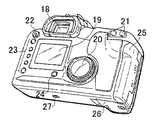
図1及び図2はデジタル一眼レフカメラの外観図を示し、図1はカメラ前方より見た斜視図であり、レンズ鏡筒を外した状態を示す。図2はカメラ背面側より見た斜視図である。 1 and 2 are external views of a digital single-lens reflex camera, and FIG. 1 is a perspective view as seen from the front of the camera, showing a state where a lens barrel is removed. FIG. 2 is a perspective view seen from the back side of the camera.
先ず、図1と図2を参照して外観される部分について説明する。1はカメラ筐体であり、撮影時に使用者がカメラを安定して握り易いように前方に突出したグリップ部1aが設けられている。2はマウント部であり、着脱可能なレンズ鏡筒3(図4及び図5参照)がカメラ本体に取り付けられる部位である。4はレンズ鏡筒3を取り外す際に押し込むレンズロック解除釦である。5はカメラ筐体内に配置されたミラーボックスで、撮影レンズを通ってきた光束を囲んだ形状である。また、撮影レンズを通った光をファインダへ導くため45°の角度に保持されるクイックリターンミラー6を内蔵している。 First, a portion that is externally described will be described with reference to FIGS. 1 and 2.
カメラ上部(正面より見て)左方には、撮影開始の起動スイッチとしてのシャッタボタン7と、撮影時の動作モードに応じてシャッタスピードやレンズ絞り値を設定するメイン操作ダイヤル8と、カメラの各動作モードを示すLCD表示パネル9と、撮影系の上面動作モード設定ボタン10が配置されている。上面動作モード設定ボタン10は、シャッタボタン7の1回の押込みで連写になるか1コマのみの撮影となるかの設定やセルフ撮影モードの設定などを行うものであり、LCD表示パネル9にその設定状況が表示されるようになっている。 To the left of the upper part of the camera (as viewed from the front), a
カメラ上部中央には、カメラ本体に対してポップアップするストロボユニット11とフラッシュ取付け用のシュー溝12とフラッシュ接点13が有り、カメラ上部右よりには撮影モード設定ダイヤル14が配置されている。 A
カメラ右側面には、開閉可能な外部端子蓋15が設けられていて、この蓋15を開けた内部には外部インターフェイスとしてビデオ信号出力用ジャック16とUSB出力用コネクタ17が納められている。 An openable / closable external
カメラ背面には、光軸中心上の上方にファインダ接眼窓18が設けられ、更にカメラ背面中央には画像表示可能なカラー液晶表示部19が設けられている。カラー液晶表示部19の横に配置されたサブ操作ダイヤル20は、メイン操作ダイヤル8の機能の補助的役割を担い、例えばカメラのAEモードでは自動露出装置により算出された適正露出値に対する露出補正量を設定するために使用される。あるいはまた、シャッタスピードとレンズ絞り値の各々を使用者の意志によって設定するマニュアルモードにおいて、メイン操作ダイヤル8でシャッタスピードを設定し、サブ操作ダイヤル20でレンズ絞り値を設定する。また、このサブ操作ダイヤル20は、カラー液晶表示部19に表示される撮影済み画像の表示選択手段としても用いられる。 A
21は背面動作モード設定ボタンであり、AEロック設定などを設定することができ、上面動作モード設定ボタン10と同様にLCD表示パネル9にその設定状況が表示されるようになっている。22はカメラの電源投入を行うためのメイン電源スイッチであり、所定角度回転させることでスイッチのON、OFFを切り替える。カラー液晶表示部19の背面より見て左わきに整列した押しボタンスイッチ23は、カラー液晶操作スイッチでカメラの各種設定を行うためのメニュー表示や撮影済み画像の表示方法の変更などを行える。 A rear operation
24は一旦記録媒体に記録された画像データを消去するための消去ボタンであり、誤って押し込んでしまうことがないようにLCD操作スイッチ24から離れて配置されている。
25は外部記録媒体であるメモリカードの挿入口を覆うための開閉可能なカード蓋であり、少量のスライド移動に加えて回動することが可能に支持されている。26は電池蓋であり、電池をカメラの底面より挿抜できるように回動可能に支持されている。27はカメラ底面に設けられた三脚取付け用ネジである。 An openable /
次に、図3〜図5を参照してカメラ内部の光学部材、電池収納室、回路基板、メモリカード装着部などの各構成部材の配置及び作用等について説明する。 Next, with reference to FIG. 3 to FIG. 5, the arrangement and operation of each component member such as an optical member inside the camera, a battery storage chamber, a circuit board, and a memory card mounting portion will be described.
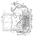
図3はカメラ背面の筐体を切断して内部を示す背面図、図4は図3のA−A線に沿って切断した水平断面図、図5は図3のB−B線に沿って切断したレンズ光軸を含む垂直断面図であり、内蔵ストロボをポップアップさせた状態を示している。 3 is a rear view showing the inside of the camera by cutting the housing on the back of the camera, FIG. 4 is a horizontal sectional view taken along the line AA in FIG. 3, and FIG. 5 is along the line BB in FIG. It is a vertical sectional view including the cut lens optical axis, and shows a state where the built-in strobe is popped up.
これらの図において、3はカメラ本体より着脱可能なレンズ鏡筒であり、撮影レンズ30を保持している。カメラ筐体1の前方に突出したグリップ部1aの内部には、電源である電池31が配置されている。 In these drawings, reference numeral 3 denotes a lens barrel that is detachable from the camera body, and holds the taking
32はフォーカルプレーンシャッタであり、クイックリターンミラー6の後方に配置され、ミラーボックス5に保持される。 A
33はペンタプリズム、34は被写体像を観察するためのファインダ接眼レンズ群である。
35は光軸Lに対して垂直な面を撮像面とするセンサチップで、被写体画像を電気撮像信号に変換する半導体である。36は前パッケージ36aと後パッケージ36bから構成され、セラミックを材料としたセンサパッケージで、センサチップ35を収納し、撮影レンズから入射された被写体像を取り込む側をカバーガラス37で密閉している。38aと38bはリードフレームで、センサチップ35とワイヤボンディングされる金属プレートであり、各々センサチップ35からの信号線及び電源線をセンサパッケージ36の外側へ引き出された複数のリード端子として機能する。
上述35〜38の部材から成る構造を総称して一般的に「撮像センサ」と呼称している。 The structure composed of the above-mentioned
39はセンサプレートで、前記撮像センサを保持する金属プレートで、撮影光束に対して十分な余裕をもつ開口部39aが形成されている。
40は上側フレキシブル基板で、一方の端部近傍において上部複数のリード端子38aと半田等で接続されている。同様に41は下側フレキシブル基板で、下部複数のリード端子38bに半田等で接続されている。上側フレキシブル基板40と下側フレキシブル基板41各々他方の端部は後述する撮像回路基板に接続される。
42はシールドプレートで、上側フレキシブル基板40と下側フレキシブル基板41をシールドするためのそれぞれの延長部42aと42b及び上側の延長部42aの背面側先端に後述するシールドケースとの接触部42cを有している。 Reference numeral 42 denotes a shield plate having
43はローパスフィルタマスクで、フォーカルプレーンシャッタ32の後方に配置され、撮影光束を規制してゴースト等の発生を防止している。
44は光学ローパスフィルタで、ローパスフィルタホルダ45に保持されており、撮影画像にモアレや擬色の発生を防止する。 An optical low-
46は粘着テープで、カバーガラス37と光学ローパスフィルタ44の間にゴミ等が進入することのないように密閉されたユニットを構成するため、ローパスフィルタホルダ45の裏面とカバーガラス37の前面との間に貼り付けられている。
上述した撮像センサを含み、39〜46の部材から成る構造を総称して、以下「撮像センサユニット」と呼称する。
The structure including the above-described imaging sensor and including
47は取付けワッシャで、後述する調整工程により厚みが選択された後、撮像センサを保持したセンサプレート39とミラーボックス5の間に挟まれていて、撮像センサユニットは、ミラーボックス5に対してビスで固定されている。
48は金属板を加工したメインシャーシで、撮像面と平行に配置されている。
このメインシャーシ48は、ミラーボックス5とビス等で強固に締結されており、ミラーボックス5と共にカメラ本体の全体的な強度を確保する骨組みを成している。また、カメラ底面部にはメインシャーシ48の一部を前方へ曲げた部位48aを有し、三脚取付けネジ27が固定されている。
The
49はモータであり、フォーカルプレーンシャッタ32のチャージやクイックリターンミラーのアップダウン動作及びストロボのポップアップ動作の駆動源であり、ミラーボックス5に保持されている。 A
50はメイン回路基板であり、撮像面と平行に配置されてメインシャーシ48に固定されている。メイン回路基板50には、撮像センサの出力信号をサンプリングして増幅し、A/D変換する電気回路、ホワイトバランス、露出調整、ガンマ補正等の画像信号に所定の処理を施す撮像信号処理回路、及びデジタル画像信号を内部メモリへ格納あるいは読み出し動作を制御するメモリコントロール回路、及び機構系の駆動等カメラ全体のシステムコントロールを行う制御回路、及び後述するカラー液晶モニタ55のドライバ回路等の画像表示回路が組み込まれていて、大きな面積が確保されている。
メイン回路基板50には、背面側上部にコネクタ51を、全面側下部にコネクタ52を実装しており、それぞれのコネクタには上述した撮像センサに接続されている上側フレキシブル基板40と下側フレキシブル基板41が接続されている。 The
更にメイン回路基板50には、前面側に撮像回路ブロックを覆う前シールドケース53が、背面側には同じく撮像回路ブロックを覆う後シールドケース54がそれぞれ取り付けられている。後ろシールドケース54には先に説明したシールドプレート42の接触部42Cに対して圧接する腕部54aを有している。 Further, a
メイン回路基板50の更に後方には、カラー液晶表示部19が配置されている。カラー液晶表示部19は、カラー液晶モニタ55と照明用光源56と筐体1の開口窓から構成されている。カラー液晶モニタ55と照明用光源56とは、板金ケース57に収納されている。 A color liquid
58はストロボ回路基板であり、ミラーボックス5の左側方に配置され、充電用のメインコンデンサ59が接続されており、このメインコンデンサ59への充電制御やストロボユニット11内の発光部60の制御を行う回路が組み込まれている。 A
61は外部記録媒体であるメモリカード、62メモリカード61が接続されるカードコネクタであり、メイン回路基板50に沿ってメインシャーシ48との間に設けられている。メモリカード61の挿抜は、カード蓋25を光軸に沿ってカメラ後方へ引いてからヒンジ25aを回動中心として反時計方向へ(図4参照)回転させて開き、カメラのグリップ側側面より行えるようになっている。
次に、以上のように構成された本実施形態におけるデジタル一眼レフカメラにおける撮像センサの位置・傾き調整について説明する。 Next, the position / tilt adjustment of the image sensor in the digital single-lens reflex camera according to the present embodiment configured as described above will be described.
センサチップ35の撮像面は、後パッケージ36bの配置面に対して、製造上、位置と傾きにばらつきがあるため、カメラを製造する上では、撮影レンズとセンサチップの撮像面との相関位置を合わせ込むための調整が必要となっている。そこで、事前に撮像センサユニットの状態でセンサチップの位置と傾きを測定し、更に撮像センサユニットを取り付けるミラーボックス5の複数ある取付け面各々の位置と傾きの測定値を考慮して取付けワッシャ47の厚みを割り出して決定する。そして、ミラーボックス5の複数ある取付け面各々に対して決定した厚みの取付けワッシャ47をしき込み、センサプレート39をビスで固定することで、撮像センサユニットの固定が完結される。 Since the image pickup surface of the
従って、前記調整により、センサチップ35は光軸Lに垂直となるものの、パッケージ36やセンサプレート39は光軸Lに対して垂直とならず、傾きをもった状態になる。 Therefore, although the
一方、大きな面積をもったメイン回路基板50はメインシャーシ48に固定されているため、カメラボディ毎に傾き量の異なる撮像センサとメイン回路基板50の間の接続は、図5に示すようなUターンしたフレキシブル基板40、41を用いてばらつきを吸収することができるようになっている。 On the other hand, since the
次に、本実施形態におけるデジタル一眼レフカメラにおけるシールド部材について詳細に説明する。 Next, the shield member in the digital single-lens reflex camera in this embodiment will be described in detail.
シールドプレート42は、センサプレート39とローパスフィルタホルダ45に挟まれて保持されている。延長部42aは、上側フレキシブル基板40と略同等の幅を有して後方へ延び、同様に延長部42bは、下側フレキシブル基板41と略同等の幅を有して後方へ延びている。各延長部の幅が各フレキの幅より同等以上の幅であれば、隣接するデジタル信号系回路やストロボ回路や電源回路等から発せられるノイズの影響が、フレキ上の配線パターンに及ぶことを防止できる。 The shield plate 42 is held between the
また、延長部42aと42bがフレキシブル基板の幅と同等の幅で後方に延びていることにより、撮像センサユニットの状態で、フレキシブル基板40と41は延長部に沿って後方へ向かって曲げられた状態にあり、メイン回路基板50上のコネクタ51及び52への差込み操作が良好に作用する。 In addition, since the
さらに、上側の延長部42aの背面側先端にあるシールドケース54との接触部42cは、上側フレキシブル基板40の幅より外側に位置しているので、上側フレキシブル基板40がシールドプレート延長部42aに沿って曲げられた形態を阻害することがなく、撮像回路基板に接続する際の作業性を良好に保つことができる。 Further, the
シールドケース54の腕部54aを板バネ形状としてシールドプレート接触部42cに対して圧接しているのは、撮像センサユニットの位置・傾き調整されて相互の位置関係にばらつきが発生してもそのばらつきを吸収することができるようするためである。 The
尚、シールドケース54の腕部54aをシールドプレート接触部42cに対して圧接のみで接続した方が接続作業及び分解作業はやり易い。しかし、反面、接続の信頼性は低い為、半田付けによって接続される方が、導通抵抗が低く抑えられ接続信頼性が高いことは言うまでもない。 Note that the connecting work and the disassembling work are easier when the
また、上記した実施例では、ローパスフィルタマスク43を単独部品として設定したものを説明したが、シールドプレート42のレンズ側開口によって撮影光束を規制するマスクとして機能させたものであってもよい。 In the above-described embodiment, the low-
1 カメラ筐体
2 マウント部
3 レンズ鏡筒
5 ミラーボックス
6 クイックリターンミラー
30 撮影レンズ
31 電池
32 フォーカルプレーンシャッタ
35 センサチップ
36 センサパッケージ
38 リードフレーム
39 センサプレート
40 上側フレキシブル基板
41 下側フレキシブル基板
42 シールドプレート
44 光学ローパスフィルタ
48 メインシャーシ
49 モータ
50 メイン回路基板
54 後シールドケース
55 カラー液晶モニタ
56 照明用光源
58 ストロボ回路基板
61 メモリカードDESCRIPTION OF
Claims (7)
Translated fromJapanese前記撮像素子を保持する保持部材と、前記保持部材に支持された第1シールド部材と、前記撮像素子から出力される電気信号を処理する撮像回路を搭載したプリント回路基板と、前記プリント回路基板上の撮像回路ブロックの少なくとも一部を覆う第2シールド部材と、前記撮像素子と前記プリント回路基板とを接続するフレキシブル配線基板とを備え、前記第1シールド部材で前記フレキシブル配線基板を覆うと共に、前記第1シールド部材と前記第2シールド部材を導電的に接続したことを特徴とする撮像装置。An imaging device having an imaging device that converts a subject image into an electrical signal, and a recording unit that records image data output from the imaging device on a recording medium,
A holding member for holding the image pickup device; a first shield member supported by the holding member; a printed circuit board on which an image pickup circuit for processing an electric signal output from the image pickup device is mounted; and the printed circuit board. A second shield member that covers at least a part of the imaging circuit block, and a flexible wiring board that connects the imaging element and the printed circuit board, and covers the flexible wiring board with the first shield member, An imaging apparatus, wherein the first shield member and the second shield member are conductively connected.
Priority Applications (1)
| Application Number | Priority Date | Filing Date | Title |
|---|---|---|---|
| JP2003294372AJP2005065014A (en) | 2003-08-18 | 2003-08-18 | Imaging device |
Applications Claiming Priority (1)
| Application Number | Priority Date | Filing Date | Title |
|---|---|---|---|
| JP2003294372AJP2005065014A (en) | 2003-08-18 | 2003-08-18 | Imaging device |
Publications (1)
| Publication Number | Publication Date |
|---|---|
| JP2005065014Atrue JP2005065014A (en) | 2005-03-10 |
Family
ID=34370962
Family Applications (1)
| Application Number | Title | Priority Date | Filing Date |
|---|---|---|---|
| JP2003294372AWithdrawnJP2005065014A (en) | 2003-08-18 | 2003-08-18 | Imaging device |
Country Status (1)
| Country | Link |
|---|---|
| JP (1) | JP2005065014A (en) |
Cited By (8)
| Publication number | Priority date | Publication date | Assignee | Title |
|---|---|---|---|---|
| KR100730062B1 (en) | 2006-03-21 | 2007-06-20 | 삼성전기주식회사 | Camera module with improved noise characteristics |
| JP2008096604A (en)* | 2006-10-11 | 2008-04-24 | Olympus Imaging Corp | Single lens reflex camera |
| JP2011166012A (en)* | 2010-02-12 | 2011-08-25 | Sony Corp | Electronic apparatus and camera |
| WO2012104929A1 (en)* | 2011-01-31 | 2012-08-09 | パナソニック株式会社 | Imaging device |
| WO2012111044A1 (en)* | 2011-02-14 | 2012-08-23 | パナソニック株式会社 | Image capturing device |
| CN102835101A (en)* | 2010-04-16 | 2012-12-19 | 松下电器产业株式会社 | Digital camera |
| JP2015046836A (en)* | 2013-08-29 | 2015-03-12 | 株式会社ニコン | Imaging apparatus |
| CN111988500A (en)* | 2019-05-22 | 2020-11-24 | 佳能株式会社 | Image forming unit and image forming apparatus |
- 2003
- 2003-08-18JPJP2003294372Apatent/JP2005065014A/ennot_activeWithdrawn
Cited By (15)
| Publication number | Priority date | Publication date | Assignee | Title |
|---|---|---|---|---|
| KR100730062B1 (en) | 2006-03-21 | 2007-06-20 | 삼성전기주식회사 | Camera module with improved noise characteristics |
| JP2008096604A (en)* | 2006-10-11 | 2008-04-24 | Olympus Imaging Corp | Single lens reflex camera |
| JP2011166012A (en)* | 2010-02-12 | 2011-08-25 | Sony Corp | Electronic apparatus and camera |
| CN102835101A (en)* | 2010-04-16 | 2012-12-19 | 松下电器产业株式会社 | Digital camera |
| WO2012104929A1 (en)* | 2011-01-31 | 2012-08-09 | パナソニック株式会社 | Imaging device |
| CN102823229A (en)* | 2011-01-31 | 2012-12-12 | 松下电器产业株式会社 | filming device |
| US8421912B2 (en) | 2011-01-31 | 2013-04-16 | Panasonic Corporation | Imaging device |
| JPWO2012104929A1 (en)* | 2011-01-31 | 2014-07-03 | パナソニック株式会社 | Imaging device |
| WO2012111044A1 (en)* | 2011-02-14 | 2012-08-23 | パナソニック株式会社 | Image capturing device |
| CN102859986A (en)* | 2011-02-14 | 2013-01-02 | 松下电器产业株式会社 | filming device |
| JPWO2012111044A1 (en)* | 2011-02-14 | 2014-07-03 | パナソニック株式会社 | Imaging device |
| US8786772B2 (en) | 2011-02-14 | 2014-07-22 | Panasonic Corporation | Imaging device |
| JP2015046836A (en)* | 2013-08-29 | 2015-03-12 | 株式会社ニコン | Imaging apparatus |
| CN111988500A (en)* | 2019-05-22 | 2020-11-24 | 佳能株式会社 | Image forming unit and image forming apparatus |
| CN111988500B (en)* | 2019-05-22 | 2023-01-06 | 佳能株式会社 | Image forming unit and image forming apparatus |
Similar Documents
| Publication | Publication Date | Title |
|---|---|---|
| JP4035488B2 (en) | Imaging device | |
| US8294816B2 (en) | Imaging apparatus containing lens mount without mirror box | |
| JPH1188750A (en) | Electronic camera | |
| JP5335977B2 (en) | Imaging device | |
| JP2005065014A (en) | Imaging device | |
| JP4521966B2 (en) | Imaging device | |
| JPH11225282A (en) | Electronic image recorder | |
| JP4194449B2 (en) | Solid-state image sensor holding structure | |
| JP4453550B2 (en) | Imaging device | |
| US20050280736A1 (en) | Image capturing apparatus | |
| JP5053873B2 (en) | Imaging device | |
| JP3012839B1 (en) | Electronic camera | |
| JP4168824B2 (en) | Imaging apparatus and camera equipped with the same | |
| JP2009211895A (en) | Electronic equipment | |
| JP2011059272A (en) | Imaging apparatus | |
| JP2007174711A (en) | Electronic image recording device | |
| JP6021528B2 (en) | Imaging device | |
| JP2006235077A (en) | Lens interchangeable camera | |
| JP2007114421A (en) | Lens unit and camera system | |
| JP2001333310A (en) | Electronic camera | |
| JP2005064693A (en) | Imaging device | |
| JP2002296658A (en) | Camera | |
| JP2009175292A (en) | Imaging device | |
| JP2006194957A (en) | Imaging apparatus, lens barrel and circuit board | |
| JP2004357122A (en) | Camera |
Legal Events
| Date | Code | Title | Description |
|---|---|---|---|
| A621 | Written request for application examination | Free format text:JAPANESE INTERMEDIATE CODE: A621 Effective date:20060810 | |
| RD04 | Notification of resignation of power of attorney | Free format text:JAPANESE INTERMEDIATE CODE: A7424 Effective date:20080207 | |
| A761 | Written withdrawal of application | Free format text:JAPANESE INTERMEDIATE CODE: A761 Effective date:20080528 |