JP2005056989A - Nonvolatile semiconductor memory device and manufacturing method thereof - Google Patents
Nonvolatile semiconductor memory device and manufacturing method thereofDownload PDFInfo
- Publication number
- JP2005056989A JP2005056989AJP2003285015AJP2003285015AJP2005056989AJP 2005056989 AJP2005056989 AJP 2005056989AJP 2003285015 AJP2003285015 AJP 2003285015AJP 2003285015 AJP2003285015 AJP 2003285015AJP 2005056989 AJP2005056989 AJP 2005056989A
- Authority
- JP
- Japan
- Prior art keywords
- gate
- contact
- insulating film
- wiring
- memory cell
- Prior art date
- Legal status (The legal status is an assumption and is not a legal conclusion. Google has not performed a legal analysis and makes no representation as to the accuracy of the status listed.)
- Pending
Links
Images


Classifications
- H—ELECTRICITY
- H10—SEMICONDUCTOR DEVICES; ELECTRIC SOLID-STATE DEVICES NOT OTHERWISE PROVIDED FOR
- H10B—ELECTRONIC MEMORY DEVICES
- H10B41/00—Electrically erasable-and-programmable ROM [EEPROM] devices comprising floating gates
- H10B41/30—Electrically erasable-and-programmable ROM [EEPROM] devices comprising floating gates characterised by the memory core region
- H10B41/35—Electrically erasable-and-programmable ROM [EEPROM] devices comprising floating gates characterised by the memory core region with a cell select transistor, e.g. NAND
- G—PHYSICS
- G11—INFORMATION STORAGE
- G11C—STATIC STORES
- G11C16/00—Erasable programmable read-only memories
- G11C16/02—Erasable programmable read-only memories electrically programmable
- G11C16/04—Erasable programmable read-only memories electrically programmable using variable threshold transistors, e.g. FAMOS
- G11C16/0483—Erasable programmable read-only memories electrically programmable using variable threshold transistors, e.g. FAMOS comprising cells having several storage transistors connected in series
- H—ELECTRICITY
- H10—SEMICONDUCTOR DEVICES; ELECTRIC SOLID-STATE DEVICES NOT OTHERWISE PROVIDED FOR
- H10B—ELECTRONIC MEMORY DEVICES
- H10B41/00—Electrically erasable-and-programmable ROM [EEPROM] devices comprising floating gates
- H10B41/30—Electrically erasable-and-programmable ROM [EEPROM] devices comprising floating gates characterised by the memory core region
- H—ELECTRICITY
- H10—SEMICONDUCTOR DEVICES; ELECTRIC SOLID-STATE DEVICES NOT OTHERWISE PROVIDED FOR
- H10B—ELECTRONIC MEMORY DEVICES
- H10B69/00—Erasable-and-programmable ROM [EPROM] devices not provided for in groups H10B41/00 - H10B63/00, e.g. ultraviolet erasable-and-programmable ROM [UVEPROM] devices
- H—ELECTRICITY
- H10—SEMICONDUCTOR DEVICES; ELECTRIC SOLID-STATE DEVICES NOT OTHERWISE PROVIDED FOR
- H10D—INORGANIC ELECTRIC SEMICONDUCTOR DEVICES
- H10D30/00—Field-effect transistors [FET]
- H10D30/60—Insulated-gate field-effect transistors [IGFET]
- H10D30/68—Floating-gate IGFETs
- H10D30/681—Floating-gate IGFETs having only two programming levels
- H—ELECTRICITY
- H10—SEMICONDUCTOR DEVICES; ELECTRIC SOLID-STATE DEVICES NOT OTHERWISE PROVIDED FOR
- H10D—INORGANIC ELECTRIC SEMICONDUCTOR DEVICES
- H10D64/00—Electrodes of devices having potential barriers
- H10D64/20—Electrodes characterised by their shapes, relative sizes or dispositions
- H10D64/27—Electrodes not carrying the current to be rectified, amplified, oscillated or switched, e.g. gates
- H10D64/311—Gate electrodes for field-effect devices
- H10D64/411—Gate electrodes for field-effect devices for FETs
- H10D64/511—Gate electrodes for field-effect devices for FETs for IGFETs
- H10D64/512—Disposition of the gate electrodes, e.g. buried gates
- H10D64/513—Disposition of the gate electrodes, e.g. buried gates within recesses in the substrate, e.g. trench gates, groove gates or buried gates
Landscapes
- Engineering & Computer Science (AREA)
- Microelectronics & Electronic Packaging (AREA)
- Non-Volatile Memory (AREA)
- Semiconductor Memories (AREA)
- Read Only Memory (AREA)
Abstract
Translated fromJapaneseDescription
Translated fromJapanese本発明は、不揮発性半導体記憶装置及びその製造方法に関し、特に、2本のメモリセル列で1本のビット線を共有し、高集積化を可能にする不揮発性半導体記憶装置及びその製造方法に関する。 The present invention relates to a nonvolatile semiconductor memory device and a method for manufacturing the same, and more particularly to a nonvolatile semiconductor memory device and a method for manufacturing the nonvolatile semiconductor memory device that enable high integration by sharing one bit line between two memory cell columns. .
従来技術の一例として、NAND型EEPROMは、各NAND列に対し、1本のビット線を有する。ビット線BLkを書き込みビット線、BLk+1/BLk−1を書き込み抑制ビット線としたとき、書き込み時は、ビット線BL側の選択ゲートトランジスタSG1に所定のゲート電位Vsgを与え、書き込みを行うビット線BLには十分低い電位VBLpgmを与える。前述のVsgは、VBLpgmに対し選択ゲートトランジスタSG1を十分オンできる電位に設定する。一方、書き込みを抑制するビット線BLk+1/BLk−1には、十分高い電位VBLinhibitを与える。VBLinhibitは、前述の選択ゲートトランジスタSG1が十分オフする電位に設定する。書き込みを行うビット線BLに十分低い電位VBLpgmを与えたNANDメモリセルトランジスタは、選択ゲートトランジスタSG1がオンしてVBLpgmがメモリセルトランジスタに伝えられるため、メモリセルトランジスタのチャネル電位が十分低下して書き込みが行われる。一方、書き込みを抑制するビット線BLk+1/BLk−1に、十分高い電位VBLinhibitを与えたNANDメモリセルトランジスタは、選択ゲートトランジスタSG1がオフになるため、メモリセルトランジスタのチャネル電位は、コントロールゲートCGとの容量結合により上昇し、書き込みは行われない。この状態が書き込み抑制状態である(非特許文献1)。
従来技術の問題点としては、NAND型メモリセルトランジスタの素子領域のピッチを2Fとしたとき、ビット線BLとビット線BL側の選択ゲートトランジスタの拡散層を接続するコンタクトのサイズは、露光技術に大きく依存し、合わせズレを考慮するとFより大きくする必要がある。ここで、Fは最小加工寸法を表す。そのため、隣り合ったビット線BLとビット線BL側の選択ゲートトランジスタの拡散層を接続するビット線コンタクトCBの間隔は、Fより小さくなり、電気的に接触してしまう危険が大きい。当然、ビット線BLについてもビット線BL側の選択ゲートトランジスタの拡散層を接続するビット線コンタクトCBと個々に接続する必要があり、加工が非常に厳しいと言った問題が生じる。 As a problem of the prior art, when the pitch of the NAND memory cell transistor element region is 2F, the size of the contact connecting the bit line BL and the diffusion layer of the select gate transistor on the bit line BL side depends on the exposure technology. It depends greatly, and it is necessary to make it larger than F in consideration of misalignment. Here, F represents the minimum processing dimension. Therefore, the distance between the bit line contact CB connecting the adjacent bit line BL and the diffusion layer of the selection gate transistor on the bit line BL side is smaller than F, and there is a high risk of electrical contact. Naturally, the bit line BL also needs to be individually connected to the bit line contact CB that connects the diffusion layer of the selection gate transistor on the bit line BL side, which causes a problem that processing is very severe.
本発明の目的は、特に、NAND型EEPROMにおいて、2列のNAND列で1本のビット線BLを共有し、ビット線BLとビット線BL側の選択ゲートトランジスタの拡散層を接続するビット線コンタクトCBをNAND列ピッチの2倍のピッチで配置することが可能な、NAND型EEPROMの高集積化を可能にする不揮発性半導体記憶装置及びその製造方法を提供することにある。 An object of the present invention is, in particular, in a NAND type EEPROM, a bit line contact that shares one bit line BL in two NAND columns and connects the bit line BL and a diffusion layer of a selection gate transistor on the bit line BL side. It is an object of the present invention to provide a non-volatile semiconductor memory device and a method for manufacturing the non-volatile semiconductor memory device capable of high integration of a NAND type EEPROM in which CBs can be arranged at a pitch twice as large as a NAND column pitch.
上記目的を達成するため、本発明の第1の特徴は、(イ)フローティングゲート、フローティングゲートの両側に配置された第一、第二のコントロールゲートをゲート構造とするメモリセルトランジスタが複数直列に接続された第一および第二のメモリセル列と、(ロ)第一のメモリセル列とビット線との間に接続された第一の選択ゲートトランジスタと、(ハ)第二のメモリセル列とビット線との間に接続された第二の選択ゲートトランジスタとを備え、(二)ビット線と第一および第二の選択ゲートトランジスタの拡散層とを接続するビット線コンタクトをメモリセル列ピッチの2倍のピッチで配置する不揮発性半導体記憶装置であることを要旨とする。 In order to achieve the above object, the first feature of the present invention is: (a) a plurality of memory cell transistors each having a floating gate and a gate structure of first and second control gates arranged on both sides of the floating gate; (B) a first select gate transistor connected between the first memory cell column and the bit line; and (c) a second memory cell column. And a second select gate transistor connected between the bit line and (2) a bit line contact connecting the bit line and the diffusion layer of the first and second select gate transistors with a memory cell column pitch The gist of the present invention is that the nonvolatile semiconductor memory device is arranged at a pitch twice as large as the above.
本発明の第2の特徴は、(イ)半導体基板上にメモリセルトランジスタおよび選択ゲートトランジスタのゲート絶縁膜となる第一の絶縁膜を形成する工程と、(ロ)メモリセルトランジスタのフローティングゲートおよび選択ゲートトランジスタのゲート電極となる第一のゲート電極を形成し、更に第二の絶縁膜を形成する工程と、(ハ)素子分離領域を形成後、メモリセルトランジスタのフローティングゲートとコントロールゲートの層間絶縁膜となる第三の絶縁膜を堆積し、メモリセルトランジスタのコントロールゲートと選択ゲートトランジスタのゲート配線となる第二のゲート電極を形成する工程と、(二)第四の絶縁膜を全面に積層形成し、第二のゲート電極上と露出した半導体基板表面上の第四の絶縁膜を除去する工程とを備える不揮発性半導体記憶装置の製造方法であることを要旨とする。 The second feature of the present invention is that (a) a step of forming a first insulating film serving as a gate insulating film of a memory cell transistor and a select gate transistor on a semiconductor substrate; (b) a floating gate of the memory cell transistor; Forming a first gate electrode to be a gate electrode of the select gate transistor and further forming a second insulating film; and (c) forming an element isolation region, and then forming an interlayer between the floating gate and the control gate of the memory cell transistor Depositing a third insulating film to be an insulating film and forming a second gate electrode to be a control wiring of the memory cell transistor and a gate wiring of the selection gate transistor; and (2) a fourth insulating film on the entire surface. Forming a stacked layer and removing the fourth insulating film on the second gate electrode and the exposed semiconductor substrate surface. And summarized in that a method of manufacturing a nonvolatile semiconductor memory device.
本発明の第3の特徴は、(イ)半導体基板上にメモリセルトランジスタのゲート絶縁膜となる第八の絶縁膜と、コントロールゲートとなる第三のゲート電極と、第九の絶縁膜とを積層形成する工程と、(ロ)素子分離領域形成後、半導体基板をエッチングして、フローティングゲートの形成予定部分を形成する工程と、(ハ)熱処理後、コントロールゲートとフローティングゲート間の層間絶縁膜となる第十の絶縁膜を堆積し、メモリセルトランジスタのチャネルプロファイルを形成後、トンネル絶縁膜として機能する第十一の絶縁膜形成部の開口を行う工程と、(二)メモリセルトランジスタのトンネル絶縁膜となる第十一の絶縁膜を形成する工程と、(ホ)フローティングゲートとなる第四のゲート電極を全面に積層し、エッチバック技術を用いて、フローティングゲートの高さを下げる工程と、(へ)第十二の絶縁膜を全面に形成した後、第三のゲート電極のみを露出させる工程と、(ト)第三のゲート電極膜を選択エッチングした後、第十三の絶縁膜を全面に堆積後、第三のゲート電極のみを露出させる工程と、(チ)第三の開口領域内の第十二の絶縁膜を選択エッチングし、第四のゲート電極を露出させる工程と、(リ)エッチング技術を用いて第三のゲート電極の上面の高さを下げ、第十四の絶縁膜を全面形成した後、フローティングゲート上面にゲート幅より狭い開口部を形成する工程とを備える不揮発性半導体記憶装置の製造方法であることを要旨とする。 The third feature of the present invention is that: (a) an eighth insulating film serving as a gate insulating film of a memory cell transistor, a third gate electrode serving as a control gate, and a ninth insulating film are formed on a semiconductor substrate; (B) a step of forming a floating gate formation portion by etching the semiconductor substrate after forming the element isolation region; and (c) an interlayer insulating film between the control gate and the floating gate after the heat treatment. Depositing a tenth insulating film to form a channel profile of the memory cell transistor and then opening an eleventh insulating film forming portion functioning as a tunnel insulating film; and (2) tunneling of the memory cell transistor The step of forming an eleventh insulating film to be an insulating film, and (e) a fourth gate electrode to be a floating gate is laminated on the entire surface to perform an etch back technique. And (f) a step of exposing only the third gate electrode after forming the twelfth insulating film on the entire surface, and (g) a third gate electrode. After selectively etching the film, depositing the thirteenth insulating film on the entire surface and then exposing only the third gate electrode, and (h) selectively etching the twelfth insulating film in the third opening region Then, the step of exposing the fourth gate electrode and the height of the upper surface of the third gate electrode are reduced by using (re) etching technology, and the entire surface of the fourteenth insulating film is formed. The present invention is summarized as a method for manufacturing a nonvolatile semiconductor memory device including a step of forming an opening narrower than a gate width.
本発明の第4の特徴は、(イ)半導体基板上に、トンネル絶縁膜となる第一の絶縁膜と、選択ゲートトランジスタのゲート電極となる第一のゲート電極と、第二の絶縁膜とを形成後、リソグラフィーとエッチングによって加工する工程と、(ロ)第一のゲート電極とコントロールゲート形成予定領域との間のゲート間絶縁膜を全面に堆積する工程と、(ハ)ゲート間絶縁膜を第一のゲート電極の側面において、リソグラフィーとエッチングにより剥離する工程と、(二)コントロールゲートおよび選択ゲートトランジスタのゲート配線となるゲート電極膜を全面に堆積した後、第一のゲート電極とコントロールゲートおよび選択ゲートトランジスタのゲート配線となるゲート電極膜とを電気的に接触させる工程とを備える不揮発性半導体記憶装置の製造方法であることを要旨とする。 The fourth feature of the present invention is: (a) a first insulating film that becomes a tunnel insulating film, a first gate electrode that becomes a gate electrode of a select gate transistor, and a second insulating film on a semiconductor substrate; (B) a step of depositing an inter-gate insulating film between the first gate electrode and the control gate formation scheduled area on the entire surface; and (c) an inter-gate insulating film. On the side surface of the first gate electrode by lithography and etching, and (2) after depositing a gate electrode film to be the gate wiring of the control gate and the selection gate transistor over the entire surface, the first gate electrode and the control And a step of electrically contacting a gate electrode film serving as a gate wiring of a gate and a selection gate transistor. And summarized in that a method of manufacturing location.
本発明によれば、NAND型EEPROMにおいて、2列のNAND列で1本のビット線BLを共有し、ビット線BLとビット線BL側の選択ゲートトランジスタの拡散層を接続するビット線コンタクトCBをNAND列ピッチの2倍のピッチで配置することが可能になり、NAND型EEPROMの高集積化を可能にする、不揮発性半導体記憶装置を提供することができる。 According to the present invention, in the NAND-type EEPROM, two bit lines share one bit line BL, and the bit line contact CB connecting the bit line BL and the diffusion layer of the selection gate transistor on the bit line BL side is connected. It is possible to provide a nonvolatile semiconductor memory device that can be arranged at a pitch twice as large as the NAND column pitch and enables high integration of the NAND type EEPROM.
NAND型EEPROMにおいて、2列のNAND列で1本のビット線BLを共有し、ビット線BLとビット線BL側の選択ゲートトランジスタの拡散層を接続するビット線コンタクトCBをNAND列ピッチの2倍のピッチで配置した。 In the NAND type EEPROM, two NAND columns share one bit line BL, and the bit line contact CB connecting the bit line BL and the diffusion layer of the selection gate transistor on the bit line BL side is twice the NAND column pitch. Arranged at a pitch of.
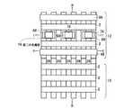
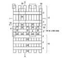
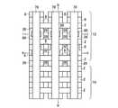
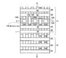
本発明の実施例1に係る不揮発性半導体記憶装置は、図1(a),(b)に示すような回路構成および素子断面構造を有する。メモリセルMCは側壁コントロールゲート型構造を有し、フローティングゲート(FG)8の両側をコントロールゲート(CG)2が挟む構成を有する。このようなメモリセルMCを直列に接続して、メモリセル列を構成している。このようなメモリセル列はビット線BLkとの間に選択ゲートトランジスタSG1若しくはSG2を備え、コントロールゲート線CG0〜CG8に平行に2本の選択ゲート線SGD1、SGD2が接続されている。ここで、図1の例では、8NAND列の例を示している。一本のNAND列に接続されるメモリセルトランジスタの数は、8個に限定されるわけではなく、図4において示すように、16NAND列であっても良い。更に、32NAND列であっても良い。これらの数は設計的事項であって、制限があるわけではない。尚、単位のメモリセルトランジスタが側壁コントロールゲート構造を有することから、コントロールゲート線CGの本数は、8NAND列の場合で9本、16NAND列の場合で17本、32NAND列の場合で33本となることも明らかである。また、このようなメモリセル列はソース線SLとの間に選択ゲートトランジスタSG3を備え、コントロールゲートCG0〜CG8に平行に1本の選択ゲート線SGSが接続されている。メモリセル列は、CG8に隣接して接続される選択ゲートトランジスタSG1若しくはSG2を介して、ビット線BLkに接続される。同様に、CG0に隣接して接続される選択ゲートトランジスタSG3を介して、ソース線SLに接続される。これらの選択ゲートトランジスタSG1、SG2、SG3の各ゲートに対して選択ゲート線SGD1、SGD2、SGSが配線されている。図1(a)より明らかなように、2本のメモリセル列は、ビット線側選択ゲートトランジスタSG1若しくはSG2を1個ずつ互い違いに接続して備えることによって、一本のビット線BLkを共有しており、ビット線コンタクトCBのスペースを節約し、結果的に集積度の向上を図ることができる。図1(b)に示すように、メモリセル列のビット線BL側は、ビット線側選択ゲートトランジスタSG1若しくはSG2の選択ゲート線SGD1もしくはSGD2を介してビット線コンタクト領域14に接続され、メモリセル列のソース線SL側は、ソース線側選択ゲートトランジスタSG3の選択ゲート線SGSを介してソース線コンタクト領域16に接続されている。メモリセル列に対して更に、このようなソース側選択ゲートトランジスタSG1若しくはSG2およびビット線側の選択ゲートトランジスタSG3までをも含めた構成を「メモリセルユニット」若しくは「メモリセルブロック」と呼ぶことにする。図1(a)の構成は、メモリセル列はNANDメモリセル構成に直列に接続されていることから、「NANDメモリセルユニット」若しくは「NANDメモリセルブロック」と呼ぶことができる。従って、図1(a)の回路構成では、NANDメモリセルユニットが2列示され、1本のビット線BLkを共有した構成を有することが明らかである。 The nonvolatile semiconductor memory device according to Example 1 of the present invention has a circuit configuration and an element cross-sectional structure as shown in FIGS. The memory cell MC has a side wall control gate type structure, and has a configuration in which the control gate (CG) 2 sandwiches both sides of the floating gate (FG) 8. Such memory cells MC are connected in series to form a memory cell column. Such a memory cell column includes a select gate transistor SG1 or SG2 between the bit line BLk, and two select gate lines SGD1 and SGD2 are connected in parallel to the control gate lines CG0 to CG8. Here, in the example of FIG. 1, an example of 8 NAND strings is shown. The number of memory cell transistors connected to one NAND string is not limited to eight, but may be 16 NAND strings as shown in FIG. Furthermore, a 32 NAND string may be used. These numbers are a matter of design and are not limited. Since the unit memory cell transistor has a sidewall control gate structure, the number of control gate lines CG is 9 in the case of 8 NAND columns, 17 in the case of 16 NAND columns, and 33 in the case of 32 NAND columns. It is also clear. In addition, such a memory cell column includes a select gate transistor SG3 between the source line SL, and one select gate line SGS is connected in parallel to the control gates CG0 to CG8. The memory cell column is connected to the bit line BLk via a select gate transistor SG1 or SG2 connected adjacent to CG8. Similarly, it is connected to the source line SL via a select gate transistor SG3 connected adjacent to CG0. Selection gate lines SGD1, SGD2, and SGS are wired to the gates of these selection gate transistors SG1, SG2, and SG3. As is clear from FIG. 1A, the two memory cell columns share bit line BLk by providing bit line side select gate transistors SG1 or SG2 alternately connected one by one. Therefore, the space of the bit line contact CB can be saved, and as a result, the degree of integration can be improved. As shown in FIG. 1B, the bit line BL side of the memory cell column is connected to the bit line contact region 14 via the select gate line SGD1 or SGD2 of the bit line side select gate transistor SG1 or SG2. The source line SL side of the column is connected to the source line contact region 16 via the selection gate line SGS of the source line side selection gate transistor SG3. Such a configuration including the source side select gate transistor SG1 or SG2 and the bit line side select gate transistor SG3 for the memory cell column is referred to as a “memory cell unit” or “memory cell block”. To do. The configuration of FIG. 1A can be called a “NAND memory cell unit” or “NAND memory cell block” because the memory cell columns are connected in series to the NAND memory cell configuration. Therefore, in the circuit configuration of FIG. 1A, it is clear that two columns of NAND memory cell units are shown and one bit line BLk is shared.
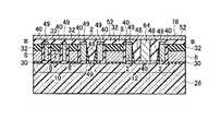
図1(b)の構造は、図1(a)の回路構成の内、1本のNANDメモリセルユニット部分を模式的に表した断面構造に相当し、尚且つ、後述する図2(b)の平面パターン図においてIV−IV線に沿う模式的断面構造を表している。pウェル若しくはシリコン半導体基板26内に形成されたn型拡散層18はメモリセルトランジスタのソース、ドレイン領域であり、このソース、ドレイン領域に挟まれたチャネル領域上に形成されて絶縁膜を介して、フローティングゲート(FG)8が配置されている。 The structure of FIG. 1B corresponds to a cross-sectional structure schematically showing one NAND memory cell unit portion in the circuit configuration of FIG. 1A, and will be described later with reference to FIG. In the plane pattern diagram, a schematic cross-sectional structure taken along line IV-IV is shown. The n-
上記例では、ビット線側選択ゲート線が2本(SGD1、SGD2)、ソース側選択ゲート線が1本(SGS)の例を示したが、これに限るものではなく、要は、ビット線コンタクト数を減少させ、コンタクト数を節約する構成であればよい。従って、ビット線側選択ゲート線の本数を3本としてもよく、更に本数を増やしても良い。ソース側選択ゲート線に関しても、1本に限ることは無く、後述するように、2本であってもよい。更に、本数を増やしても良い。 In the above example, two bit line side select gate lines (SGD1, SGD2) and one source side select gate line (SGS) are shown. However, the present invention is not limited to this. Any configuration that reduces the number and saves the number of contacts may be used. Therefore, the number of bit line side select gate lines may be three, or the number may be increased. The number of source side select gate lines is not limited to one, and may be two as will be described later. Further, the number may be increased.
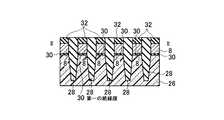
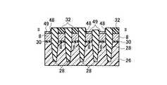
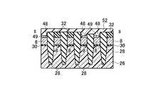
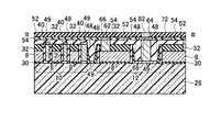
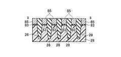
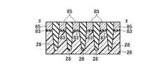
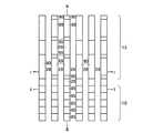
図2(a),(b)は本発明の実施例1に係る不揮発性半導体記憶装置の模式的回路構成図と模式的平面パターン図を示す。図2(a),(b)はそれぞれ対応するように描かれており、ビット線コンタクトCBは2本のNANDメモリセルユニットで1個を共有し、従って、ビット線BLkは2本のNANDメモリセルユニットで1本配置すれば済む様子が描かれている。図2(b)のI−I線、II−II線、III−III線に沿う素子断面構造は、それぞれ、図3(a)、図3(b)、図3(c)に示される通りである。更に、IV−IV線の沿う素子断面構造は図1(b)に模式的に示された通りである。図3(a)より明らかなように、各ビット線毎にビット線コンタクトCBを配置する場合に比べ、ビット線コンタクトCB間のスペースに余裕をとることができる。特に、55nmスケール等の微細な不揮発性半導体記憶装置においては、ビット線コンタクトCBの配置上、コンタクトホール間の寸法が微細なため、充分な合せ余裕がとれず、歩留まりの低下等の問題がある。本発明の実施例1の構成により、これらの問題を解決することができる。 2A and 2B are a schematic circuit configuration diagram and a schematic plan pattern diagram of the nonvolatile semiconductor memory device according to the first embodiment of the invention. FIGS. 2A and 2B are drawn to correspond to each other, and the bit line contact CB shares one with two NAND memory cell units. Therefore, the bit line BLk has two NAND memories. It shows how one cell unit can be arranged. The element cross-sectional structures along the II, II-II, and III-III lines in FIG. 2B are as shown in FIGS. 3A, 3B, and 3C, respectively. It is. Furthermore, the element cross-sectional structure along the IV-IV line is as schematically shown in FIG. As is clear from FIG. 3A, it is possible to make room for the space between the bit line contacts CB as compared with the case where the bit line contact CB is arranged for each bit line. In particular, in a fine nonvolatile semiconductor memory device of 55 nm scale or the like, there is a problem in that a sufficient alignment margin cannot be obtained due to the arrangement of the bit line contacts CB, and the yield is reduced. . These problems can be solved by the configuration of the first embodiment of the present invention.
図3(b)から明らかなように、図2(b)のII−II線に沿う断面構造は、フローティングゲート(FG)8部分における断面構造である。トンネルゲート絶縁膜として動作する第一のゲート絶縁膜30上にフローティングゲート(FG)8が配置されている。チャネル領域はpウェル26と共通領域であるが、素子分離領域28によって挟まれて形成される。フローティングゲート(FG)8上には第二の絶縁膜32が形成され、更に全体を第五の絶縁膜52が覆っている。 As apparent from FIG. 3B, the cross-sectional structure taken along the line II-II in FIG. 2B is a cross-sectional structure in the floating gate (FG) 8 portion. A floating gate (FG) 8 is disposed on the first
図3(c)から明らかなように、図2(b)のIII−III線に沿う断面構造は、コントロールゲート(CG)2部分における断面構造である。ゲート絶縁膜として動作する第三の絶縁膜40上にコントロールゲート(CG)2が配置されている。n型拡散層18はメモリセルトランジスタのソース、ドレイン領域であるが、素子分離領域28によって挟まれて形成される。コントロールゲート(CG)2上には金属サリサイド膜49が形成され、更に全体を第五の絶縁膜52が覆っている。尚、図18等で後述するように、第三の絶縁膜40はゲート間絶縁膜40としても機能する。図3(c)では、コントロールゲート2の側壁部に形成されるゲート間絶縁膜40は、説明を簡単にするために省いている。実際上は、後述する製造方法において、構造は詳細に説明する。また、図2(b)に示されるソース線コンタクトCSは、ソース線SLに対して電気的に共通に接続されるため、ビット線コンタクトCB相互間の電気的な分離という問題点は、ソース線コンタクトCS相互間には存在しない。 As is clear from FIG. 3C, the cross-sectional structure taken along line III-III in FIG. 2B is a cross-sectional structure in the control gate (CG) 2 portion. A control gate (CG) 2 is disposed on the third insulating
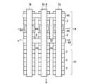
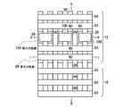
本発明の実施例1に係る不揮発性半導体記憶装置のマトリックス回路構成は、例えば、図4に示すように、6本のNANDメモリセルユニット24a〜24fと、制御ゲート線CG1〜CG17と、選択ゲート線SG01〜SG03と、ビット線BLk−1、BLk、BLk+1と、ソース線SLと、ビット線駆動回路1と、制御ゲート線駆動回路20と、選択ゲート線駆動回路21と、ソース線駆動回路22とから構成される。NANDメモリセルユニット24a〜24fは、図4の例では、16個直列に接続されたメモリセルトランジスタと、制御ゲート線CG17に隣接して配置される選択ゲート線SG01若しくはSG02を備える1個のビット線側選択ゲートトランジスタSG1若しくはSG2と、制御ゲート線CG1に隣接して配置される選択ゲート線SG03を備える1個のソース線側選択ゲートトランジスタSG3とを備え、上記選択ゲートトランジスタを介してそれぞれビット線BL、ソース線SLに接続している。また、図4において、例えば、2本の制御ゲート線CG12、CG13に挟まれる全メモリセルトランジスタ23によって、ページモードにおける1ページ分に相当するメモリセルの一行分を定義することもできる。 The matrix circuit configuration of the nonvolatile semiconductor memory device according to the first embodiment of the invention includes, for example, six NAND
(動作モード)
以下、図5(a),(b)〜図8(a),(b)を用いて、本発明の実施例1に係る不揮発性半導体記憶装置の動作方法を説明する。ここで、説明を容易にするために、図4のNANDメモリセルユニット24a〜24fをそれぞれNAND列1〜NAND列6と呼ぶことにする。図5(a),(b)〜図8(a),(b)の各図には、ビット線BLK−1,BLk,BLk+1の電圧波形、選択ゲートトランジスタSG1,SG2,SG3のゲート電圧波形、選択および非選択ワード線(コントロールゲート線)WLの電圧波形が示されている。(action mode)
Hereinafter, an operation method of the nonvolatile semiconductor memory device according to the first embodiment of the present invention will be described with reference to FIGS. 5A and 5B to FIGS. 8A and 8B. Here, for ease of explanation, the NAND
(書き込み動作モード)
NAND列3のあるメモリセルに書き込みを行なう場合の動作波形を図5(a)に示す。また、NAND列4のあるメモリセルに書き込みを行なう場合の動作波形を図5(b)に示す。(Write operation mode)
FIG. 5A shows an operation waveform when writing to a memory cell in the
NAND列3を書き込みNANDメモリセルとし、NAND列1,2,4,5,6を書き込み抑制NAND列とする。 The
図5(a)に示すように、ビット線BL側の選択ゲートトランジスタSG1,2に与えるゲート電圧波形によって、NAND列1,2,3,4,5,6にビット線BLからVdd−Vth(SG)を転送し、チャネル電位を上昇させた後、図5(a)に示すように、ビット線BLkと選択ゲートトランジスタSG1に与える電圧波形によって、NAND列3のメモリセルトランジスタのチャネル電位は十分低下し、書き込みが行われる。但し、Vsgdは、Vblに対し、十分オフする電圧に設定する。一方、NAND列1,2,4,5,6のメモリセルトランジスタは選択ゲートトランジスタSG1,SG2がオフになるため、メモリセルトランジスタのチャネル電位は、Vdd−Vth(SG)に加えコントロールゲートCGとの容量結合により、さらに上昇し書き込みは行われない。 As shown in FIG. 5A, depending on the gate voltage waveform applied to the select gate transistors SG1 and SG2 on the bit line BL side,
(読み出し動作モード)
(ビット線シールド使用時)
ビット線シールド使用時における読み出し動作を図6(a),(b)及び図7(a),(b)を用いて説明する。又、ビット線シールド不使用時における読み出し動作を図8(a),(b)を用いて説明する。(Read operation mode)
(When using bit line shield)
A read operation when the bit line shield is used will be described with reference to FIGS. 6 (a) and 6 (b) and FIGS. 7 (a) and 7 (b). A read operation when the bit line shield is not used will be described with reference to FIGS.
NAND列3のあるメモリセルトランジスタを読み出す場合の動作波形を図6(a)に示す。また、NAND列4のあるメモリセルトランジスタを読み出す場合の動作波形を図6(b)に示す。 FIG. 6A shows an operation waveform when a memory cell transistor in the
図6(a)において、表示Aはビット線BLk上における充電状態を示し、表示Bは選択メモリセルが書き込み済みメモリセルの場合に、選択ゲートトランジスタSG3を開放状態(Vsg)として、ビット線BLk上における放電状態を示す。又、ビット線BLk上の非放電時の波形は、点線で示されている通りである。 In FIG. 6A, a display A shows a charged state on the bit line BLk, and a display B shows that the selected gate transistor SG3 is in an open state (Vsg) when the selected memory cell is a written memory cell. The discharge state above is shown. The waveform at the time of non-discharge on the bit line BLk is as shown by the dotted line.
図6(b)において、表示Cはビット線BLk上における充電状態を示し、表示Dは読み出しメモリセルが書き込み済みメモリセルの場合に、選択ゲートトランジスタSG3を開放状態(Vsg)として、ビット線BLk上における放電状態を示す。又、ビット線BLk上の非放電時の波形は、点線で示されている通りである。 In FIG. 6B, the display C shows the charge state on the bit line BLk, and the display D shows the bit line BLk when the read memory cell is a written memory cell and the select gate transistor SG3 is opened (Vsg). The discharge state above is shown. The waveform at the time of non-discharge on the bit line BLk is as shown by the dotted line.
NAND列2,6のあるメモリセルを読み出す場合の動作波形を図7(a)に示す。また、NAND列1,5のあるメモリセルを読み出す場合の動作波形を図7(b)に示す。 FIG. 7A shows an operation waveform when a memory cell having the NAND strings 2 and 6 is read. Further, FIG. 7B shows an operation waveform when a memory cell having the NAND strings 1 and 5 is read.
図7(a)において、表示Eはビット線BLk−1上における充電状態を示し、表示Fは選択メモリセルが書き込み済みメモリセルの場合に、選択ゲートトランジスタSG3を開放状態(Vsg)として、ビット線BLk−1上における放電状態を示す。また、表示Gはビット線BLk+1上における充電状態を示し、表示Hは選択メモリセルが書き込み済みメモリセルの場合に、選択ゲートトランジスタSG3を開放状態(Vsg)として、ビット線BLk+1上における放電状態を示す。又、ビット線BLk−1上の非放電時の波形は、点線で示されている通りである。又、ビット線BLk+1上の非放電時の波形は、点線で示されている通りである。 In FIG. 7A, the display E shows the state of charge on the bit line BLk-1, and the display F shows that the selected gate transistor SG3 is in an open state (Vsg) when the selected memory cell is a written memory cell. The discharge state on line BLk-1 is shown. In addition, a display G indicates a charging state on the bit
図7(b)において、表示Iはビット線BLk−1上における充電状態を示し、表示Jは選択メモリセルが書き込み済みメモリセルの場合に、選択ゲートトランジスタSG3を開放状態(Vsg)として、ビット線BLk−1上における放電状態を示す。また、表示Kはビット線BLk+1上における充電状態を示し、表示Lは選択メモリセルが書き込み済みメモリセルの場合に、選択ゲートトランジスタSG3を開放状態(Vsg)として、ビット線BLk+1上における放電状態を示す。又、ビット線BLk−1上の非放電時の波形は、点線で示されている通りである。又、ビット線BLk+1上の非放電時の波形は、点線で示されている通りである。 In FIG. 7B, the display I indicates the state of charge on the bit line BLk−1, and the display J indicates that the selected gate transistor SG3 is opened (Vsg) when the selected memory cell is a written memory cell. The discharge state on line BLk-1 is shown. In addition, the display K shows the charge state on the bit
(ビット線シールド不使用時)
図8(a),(b)を用いて、ビット線シールド不使用時における読み出し動作を説明する。(When not using bit line shield)
A read operation when the bit line shield is not used will be described with reference to FIGS.
NAND列1,3,5に配置されたあるメモリセルを読み出す場合の動作波形を図8(a)に示す。また、NAND列2,4,6に配置されたあるメモリセルを読み出す場合の動作波形を図8(b)に示す。ビット線シールドを使用しないことから、図8の動作波形から明らかのように、隣り合うビット線を同時に読み出す動作を行なっている。 FIG. 8A shows an operation waveform when a certain memory cell arranged in the NAND strings 1, 3, and 5 is read. Further, FIG. 8B shows an operation waveform when a certain memory cell arranged in the NAND strings 2, 4, and 6 is read. Since the bit line shield is not used, as is apparent from the operation waveform of FIG. 8, an operation of simultaneously reading adjacent bit lines is performed.
図8(a)において、表示Aはビット線BLk上における充電状態を示し、表示Bは選択メモリセルが書き込み済みメモリセルの場合に、選択ゲートトランジスタSG3を開放状態(Vsg)として、ビット線BLk上における放電状態を示す。又、ビット線BLk上の非放電時の波形は、点線で示されている通りである。表示Eはビット線BLk−1上における充電状態を示し、表示Fは選択メモリセルが書き込み済みメモリセルの場合に、選択ゲートトランジスタSG3を開放状態(Vsg)として、ビット線BLk−1上における放電状態を示す。また、表示Gはビット線BLk+1上における充電状態を示し、表示Hは選択メモリセルが書き込み済みメモリセルの場合に、選択ゲートトランジスタSG3を開放状態(Vsg)として、ビット線BLk+1上における放電状態を示す。又、ビット線BLk−1上の非放電時の波形は、点線で示されている通りである。又、ビット線BLk+1上の非放電時の波形は、点線で示されている通りである。 In FIG. 8A, the display A shows the charged state on the bit line BLk, and the display B shows that the selected gate transistor SG3 is in an open state (Vsg) when the selected memory cell is a written memory cell. The discharge state above is shown. The waveform at the time of non-discharge on the bit line BLk is as shown by the dotted line. The display E shows the charge state on the bit line BLk-1, and the display F shows the discharge on the bit line BLk-1 with the select gate transistor SG3 open (Vsg) when the selected memory cell is a written memory cell. Indicates the state. In addition, a display G indicates a charging state on the bit
図8(b)において、表示Cはビット線BLk上における充電状態を示し、表示Dは読み出しメモリセルが書き込み済みメモリセルの場合に、選択ゲートトランジスタSG3を開放状態(Vsg)として、ビット線BLk上における放電状態を示す。又、ビット線BLk上の非放電時の波形は、点線で示されている通りである。表示Iはビット線BLk−1上における充電状態を示し、表示Jは選択メモリセルが書き込み済みメモリセルの場合に、選択ゲートトランジスタSG3を開放状態(Vsg)として、ビット線BLk−1上における放電状態を示す。また、表示Kはビット線BLk+1上における充電状態を示し、表示Lは選択メモリセルが書き込み済みメモリセルの場合に、選択ゲートトランジスタSG3を開放状態(Vsg)として、ビット線BLk+1上における放電状態を示す。又、ビット線BLk−1上の非放電時の波形は、点線で示されている通りである。又、ビット線BLk+1上の非放電時の波形は、点線で示されている通りである。ビット線シールドを使用しない場合には、隣り合うビット線同士の相互干渉を抑制する動作範囲において、メモリセルアレイを効率よく動作させることができる。又、ビット線シールドを使用しない場合には、ビット線に対してランダムに電圧を印加することができるという利点も存在する。 In FIG. 8B, the display C shows the charge state on the bit line BLk, and the display D shows the bit line BLk when the read memory cell is a written memory cell and the select gate transistor SG3 is opened (Vsg). The discharge state above is shown. The waveform at the time of non-discharge on the bit line BLk is as shown by the dotted line. The display I shows the charge state on the bit line BLk-1, and the display J shows the discharge on the bit line BLk-1 with the select gate transistor SG3 open (Vsg) when the selected memory cell is a written memory cell. Indicates the state. In addition, the display K shows the charge state on the bit
(実施例1の変形例)
本発明の実施例1に係る不揮発性半導体記憶装置の変形例は、図9に示すように、NANDメモリセルユニット24a〜24fを含むNANDメモリセルアレイ24と、2本のビット側選択ゲート線SG01、SG02と、2本のソース線側選択ゲート線SG03、SG04と、例示としてのビット線BLk−1、BLk、BLk+1と、ビット線駆動回路1と、制御ゲート線駆動回路20と、選択ゲート線駆動回路21と、ソース線駆動回路22とから構成される。図8の構成には、非選択制御ゲート線CGと選択制御ゲート線CGが区別して示されているが、それぞれ制御ゲート線駆動回路20に接続される点は、図4と同様である。(Modification of Example 1)
As shown in FIG. 9, a modification of the nonvolatile semiconductor memory device according to the first embodiment of the present invention includes a NAND
実施例1の変形例においては、図9に示すように、図4に示した実施例1と比較して、ソース側選択ゲート線を1本増やし、SG03、SG04として、2本配置した点に特徴を有する。このように構成することによって、回路構成上、ビット線側とソース線側をほぼ対称に構成することができ、パターンレイアウト構成が容易となる。また、回路動作上の自由度を増すこともでき、後述する通り、例えば、書き込み時間を短縮できるという利点もあり、またリードディスターブに対する負荷を低減することができるという利点もある。 In the modification of the first embodiment, as shown in FIG. 9, compared to the first embodiment shown in FIG. 4, the source side selection gate line is increased by one, and two lines SG03 and SG04 are arranged. Has characteristics. With this configuration, the bit line side and the source line side can be configured almost symmetrically in the circuit configuration, and the pattern layout configuration is facilitated. In addition, the degree of freedom in circuit operation can be increased. As described later, for example, there is an advantage that the writing time can be shortened, and there is also an advantage that the load on the read disturb can be reduced.
(動作モード)
以下、図10(a),(b)〜図13(a),(b)を用いて、本発明の実施例1の変形例に係る不揮発性半導体記憶装置の動作方法を説明する。図10(a),(b)〜図13(a),(b)の各図には、ビット線BLK−1,BLk,BLk+1の電圧波形、選択ゲートトランジスタSG1,SG2,SG3,SG4のゲート電圧波形、選択および非選択ワード線(コントロールゲート線)WLの電圧波形および共通ソース線SLの電圧波形が示されている。(action mode)
Hereinafter, an operation method of the nonvolatile semiconductor memory device according to the modification of the first embodiment of the present invention will be described with reference to FIGS. 10 (a) and 10 (b) to FIGS. 13 (a) and 13 (b). 10A, 10B, 13A, and 13B show voltage waveforms of the bit lines BLK-1, BLk, and BLk + 1, and gates of the select gate transistors SG1, SG2, SG3, and SG4. A voltage waveform, a voltage waveform of a selected and non-selected word line (control gate line) WL, and a voltage waveform of a common source line SL are shown.
(書き込み動作モード)
NAND列3のあるメモリセルに書き込みを行なう場合の動作波形を図10(a)に示す。また、NAND列4のあるメモリセルに書き込みを行なう場合の動作波形を図10(b)に示す。(Write operation mode)
FIG. 10A shows operation waveforms when writing to a memory cell in the
図10(a)に示すように、ビット線BL側の選択ゲートトランジスタSG1に与えるゲート電圧波形によって、NAND列2,6にビット線BLからVdd−Vth(SG)を転送し、NAND列3にビット線BLから0Vを転送している。共通ソース線SL側の選択ゲートトランジスタSG3に与えるゲート電圧波形によって、NAND列1,4,5に共通ソース線SLからVdd−Vth(SG)を転送している。 As shown in FIG. 10A, Vdd−Vth (SG) is transferred from the bit line BL to the NAND strings 2 and 6 and transferred to the
図10(b)に示すように、ビット線BL側の選択ゲートトランジスタSG2に与えるゲート電圧波形によって、NAND列1,5にビット線BLからVdd−Vth(SG)を転送し、NAND列4にビット線BLから0Vを転送している。共通ソース線SL側の選択ゲートトランジスタSG4に与えるゲート電圧波形によって、NAND列2,3,6に共通ソース線SLからVdd−Vth(SG)を転送している。 As shown in FIG. 10B, Vdd−Vth (SG) is transferred from the bit line BL to the NAND strings 1 and 5 and transferred to the
図4に示す回路構成を有する実施例1においては、誤書き込みを防ぐために、書き込み前に、書き込み禁止メモリセルのあるNAND列に、Vdd−Vth(SG)なる電圧を転送し、チャネル電位を上昇させている。その結果として、書き込みメモリセルのあるNAND列は、一度充電されたVdd−Vth(SG)なる電圧を放電し、チャネル電位を下げる動作が必要である。これに対して、図9に示す回路構成を有する実施例1の変形例においては、ソース側の選択ゲート線を2本とし、ビット線側の選択ゲート線と合わせて合計4本とすることによって、書き込み禁止メモリセルのあるNAND列へはVdd−Vth(SG)なる電圧を、書き込みメモリセルのあるNAND列へは0(V)を、同時に転送することが可能なため、書き込み時間を短縮することができる。 In the first embodiment having the circuit configuration shown in FIG. 4, in order to prevent erroneous writing, a voltage of Vdd−Vth (SG) is transferred to the NAND string where the write-inhibited memory cells are present before writing, and the channel potential is increased. I am letting. As a result, a NAND string having a write memory cell needs to operate to discharge a voltage of Vdd−Vth (SG) once charged and lower the channel potential. On the other hand, in the modification of the first embodiment having the circuit configuration shown in FIG. 9, the number of source-side selection gate lines is two, and the total of the number of selection gate lines on the bit line side is four. Since the voltage Vdd-Vth (SG) can be transferred simultaneously to the NAND string having the write-inhibited memory cell and 0 (V) can be simultaneously transferred to the NAND string having the write memory cell, the writing time can be shortened. be able to.
(読み出し動作モード)
NAND列3のあるメモリセルを読み出す場合の動作波形を図11(a)に示す。また、NAND列4のあるメモリセルを読み出す場合の動作波形を図11(b)に示す。(Read operation mode)
FIG. 11A shows operation waveforms when a memory cell in the
図11(a)において、表示Aはビット線BLk上における充電状態を示し、表示Bは選択メモリセルが書き込み済みメモリセルの場合に、選択ゲートトランジスタSG4を開放状態(Vsg)として、ビット線BLk上における放電状態を示す。即ち、ソース線側選択ゲート線SG04に与える動作波形によって、ビット線BLkからNAND列3に充電した電位を共通ソース線SLに放電している。又、ビット線BLk上の非放電時の波形は、点線で示されている通りである。 In FIG. 11A, the display A shows the charge state on the bit line BLk, and the display B shows that the select gate transistor SG4 is in an open state (Vsg) when the selected memory cell is a written memory cell. The discharge state above is shown. That is, the potential charged in the
図11(b)において、表示Cはビット線BLk上における充電状態を示し、表示Dは選択メモリセルが書き込み済みメモリセルの場合、選択ゲートトランジスタSG3を開放状態(Vsg)として、ビット線BLk上における放電状態を示す。即ち、ソース線側選択ゲート線SG03に与える動作波形によって、ビット線BLkからNAND列4に充電した電位を共通ソース線SLに放電している。又、ビット線BLk上の非放電時の波形は、点線で示されている通りである。 In FIG. 11B, the display C shows the state of charge on the bit line BLk, and the display D shows the state on the bit line BLk with the select gate transistor SG3 open (Vsg) when the selected memory cell is a written memory cell. The discharge state in is shown. That is, the potential charged in the
NAND列2,6のあるメモリセルを読み出す場合の動作波形を図12(a)に示す。また、NAND列1,5のあるメモリセルを読み出す場合の動作波形を図12(b)に示す。 FIG. 12A shows an operation waveform when a memory cell having the NAND strings 2 and 6 is read. Further, FIG. 12B shows an operation waveform when a memory cell having the NAND strings 1 and 5 is read.
図12(a)において、表示Eはビット線BLk−1上における充電状態を示し、表示Fは選択メモリセルが書き込み済みメモリセルの場合、選択ゲートトランジスタSG4を開放状態(Vsg)として、ビット線BLk−1上における放電状態を示す。また、表示Gはビット線BLk+1上における充電状態を示し、表示Hは選択メモリセルが書き込み済みメモリセルの場合に、選択ゲートトランジスタSG4を開放状態(Vsg)として、ビット線BLk+1上における放電状態を示す。即ち、ソース線側選択ゲート線SG04に与える動作波形によって、ビット線BLkからNAND列2,6に充電した電位を共通ソース線SLに放電している。又、ビット線BLk−1上の非放電時の波形は、点線で示されている通りである。又、ビット線BLk+1上の非放電時の波形は、点線で示されている通りである。 In FIG. 12A, the display E shows the state of charge on the bit line BLk-1, and the display F shows that the selected gate transistor SG4 is opened (Vsg) when the selected memory cell is a written memory cell. The discharge state on BLk-1 is shown. In addition, a display G indicates a charged state on the bit
図12(b)において、表示Iはビット線BLk−1上における充電状態を示し、表示Jは選択メモリセルが書き込み済みメモリセルの場合に、選択ゲートトランジスタSG3を開放状態(Vsg)として、ビット線BLk−1上における放電状態を示す。また、表示Kはビット線BLk+1上における充電状態を示し、表示Lは選択メモリセルが書き込み済みメモリセルの場合に、選択ゲートトランジスタSG3を開放状態(Vsg)として、ビット線BLk+1上における放電状態を示す。即ち、ソース線側選択ゲート線SG03に与える動作波形によって、ビット線BLkからNAND列1,5に充電した電位を共通ソース線SLに放電している。又、ビット線BLk−1上の非放電時の波形は、点線で示されている通りである。又、ビット線BLk+1上の非放電時の波形は、点線で示されている通りである。 In FIG. 12B, the display I indicates the state of charge on the bit line BLk-1, and the display J indicates that the selected gate transistor SG3 is in an open state (Vsg) when the selected memory cell is a written memory cell. The discharge state on line BLk-1 is shown. In addition, the display K shows the charge state on the bit
図4に示す回路構成を有する実施例1においては、共通ソース線SLの電位0(V)がソース側選択ゲートトランジスタSG3の開放時(Vsg)にすべてNAND列へ転送され、結果として全てのNAND列のチャネル電位が0(V)となり、リードディスターブに対する負荷が高くなる。但し、非読み出しNAND列で書き込みメモリセルの制御ゲート線(コントロールゲート線)CGが選択(0V)されていれば、ソース側選択ゲート線SG03からそのメモリセルまでのチャネル電位が0(V)となる。これに対して、図9に示す回路構成を有する実施例1の変形例においては、ソース側の選択ゲート線を2本とし、ビット線側の選択ゲート線と合せて合計4本とすることによって、ソース線側選択ゲート線(SG03若しくはSG04)開放時に0(V)が転送されるNAND列は、半分のNAND列に減少することができ、また非選択選択ゲート線(SG03若しくはSG04)に繋がるNAND列のチャネル電位はフローティング状態になるため、リードディスターブに対する負荷を低減することができる。 In the first embodiment having the circuit configuration shown in FIG. 4, the potential 0 (V) of the common source line SL is all transferred to the NAND string when the source side selection gate transistor SG3 is opened (Vsg), and as a result, all NANDs The channel potential of the column becomes 0 (V), and the load on the read disturb increases. However, if the control gate line (control gate line) CG of the write memory cell is selected (0 V) in the non-read NAND string, the channel potential from the source side select gate line SG03 to the memory cell is 0 (V). Become. On the other hand, in the modification of the first embodiment having the circuit configuration shown in FIG. 9, the number of source-side selection gate lines is two, and the total of the number of selection gate lines on the bit line side is four. The NAND string to which 0 (V) is transferred when the source line side selection gate line (SG03 or SG04) is opened can be reduced to a half NAND string, and is connected to the non-selected selection gate line (SG03 or SG04). Since the channel potential of the NAND string is in a floating state, the load on the read disturb can be reduced.
尚、図11及び図12に示した読み出し動作においては、ビット線シールドを使用する場合について説明したが、ビット線シールドを使用しない場合についても、前述の図8の説明と同様に行なうことができることは明らかである。動作は、図8に示した波形と同様であるため説明は省略する。ビット線シールドを使用しない場合には、隣り合うビット線同士の相互干渉を抑制する動作範囲において、メモリセルアレイを効率よく動作させることができる。又、ビット線シールドを使用しない場合には、ビット線に対してランダムに電圧を印加することができるという利点も存在する。 In the read operation shown in FIGS. 11 and 12, the case where the bit line shield is used has been described. However, the case where the bit line shield is not used can be performed in the same manner as described above with reference to FIG. Is clear. The operation is the same as the waveform shown in FIG. When the bit line shield is not used, the memory cell array can be efficiently operated within an operation range in which mutual interference between adjacent bit lines is suppressed. In addition, when the bit line shield is not used, there is an advantage that a voltage can be randomly applied to the bit line.
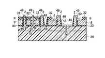
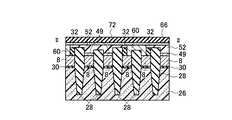
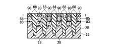
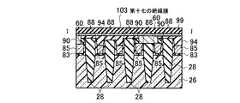
図13乃至図48を用いて、本発明の実施例2に係る不揮発性半導体記憶装置として、NAND型EEPROMのメモリセル領域10、選択ゲートトランジスタ領域12、及びビット線BL形成の製造方法を平面パターン図、I−I方向断面図、II−II方向断面図、III−III方向断面図を用いて説明する。 A manufacturing method for forming a NAND type EEPROM
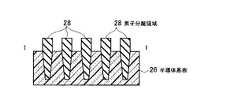
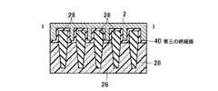
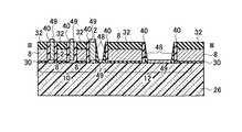
(a)まず、シリコン半導体基板26上にメモリセルトランジスタのトンネル酸化膜となり選択ゲートトランジスタのゲート酸化膜となる第一の絶縁膜30を形成し、全面にメモリセルトランジスタのフローティングゲート8と選択ゲートトランジスタのゲート電極となる第一のゲート電極8の膜を堆積し、第二の絶縁膜32を堆積する。第二の絶縁膜32の選択には、第一のゲート電極8の膜とのエッチング選択比が得られることが最低条件であるが、後述する素子分離領域28用絶縁膜と、第二のゲート電極2との化学的機械的研磨(CMP)技術工程における研磨選択比が得られる絶縁膜であることがより望ましい。その後、リソグラフィ技術とエッチング技術を用いて素子分離溝を形成し、素子分離領域28用絶縁膜を全面に堆積した後、CMP技術を用いて、素子分離領域28を形成する。その後、リソグラフィ技術とエッチング技術を用いて、図13乃至図16に示す構造を形成する。(A) First, a first insulating
(b)その後、メモリセルトランジスタのフローティングゲート8とコントロールゲート2間の層間絶縁膜となる第三の絶縁膜40を堆積し、メモリセルトランジスタのコントロールゲート2と選択ゲートトランジスタのゲート配線となる第二のゲート電極2の膜を堆積し、CMP技術を用いて、図17乃至図20に示す構造を形成する。(B) Thereafter, a third insulating
(c)次に、選択ゲートトランジスタ領域12を形成する工程の一部として、リソグラフィ技術とエッチング技術を用いて、図21乃至図24に示す構造を形成する。(C) Next, as a part of the process of forming the select
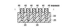
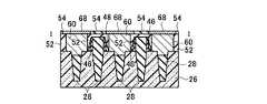
(d)次に、金属サリサイド膜49のサリサイド抑制膜として使用する第四の絶縁膜48を全面に積層形成し、選択エッチング技術を用いて、第二のゲート電極2の膜上面と露出したシリコン半導体基板26表面の第四の絶縁膜48を除去し、図25乃至図28に示す構造を形成する。第四の絶縁膜48の選択には、第一のゲート電極8の膜と第二のゲート電極2の膜とのエッチング選択比が得られる絶縁膜であることを考慮する。(D) Next, a fourth insulating
(e)次に、リソグラフィ技術とエッチング技術を用いて、第一の開口領域50内の第二の絶縁膜32を除去する。この時、第一の開口領域50内の第三の絶縁膜40も同様に除去され、後述する金属サリサイド工程にて、第一の開口領域50内の第三の絶縁膜40を介して隣接する第一のゲート電極8の膜と第二のゲート電極2の膜が金属サリサイド膜49を介して電気的に接続可能となる。その後、全面に金属薄膜を形成して加熱を行い、第二の絶縁膜32と第四の絶縁膜48をサリサイド抑制膜として使用することにより、第二のゲート電極2の膜上面、第一の開口領域50内の第一のゲート電極8の膜上面と露出したシリコン半導体基板26表面のみに金属サリサイド膜49を形成することが可能である(図29乃至図32)。(E) Next, the second insulating
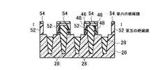
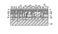
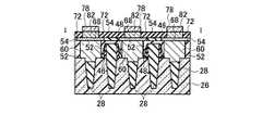
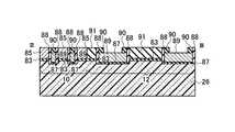
(f)次に、層間絶縁膜として第五の絶縁膜52を全面に積層し、CMP技術や化学的ドライエッチング(CDE)技術を用いて平坦化し、第六の絶縁膜54を全面に積層する。その後、リソグラフィ技術とエッチング技術を用いて、第一のコンタクト溝56と第二のコンタクト溝58を形成し、図33乃至図36に示す構造を形成する。(F) Next, a fifth insulating
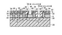
(g)次に、図37乃至図40に示すように、リソグラフィ技術とエッチング技術を用いて、第六の絶縁膜54のみを一部除去し、第一の配線溝と第二の配線溝を形成した後、全面に第一の金属膜60を堆積し、CMP技術を用いて、第六の絶縁膜54まで研磨し、第一のコンタクト62と第二のコンタクト64と第一の配線66と第二の配線68を形成する。この時、第一のコンタクト62に接する隣り合うフローティングゲート8は、第一のコンタクト62を介して電気的に接続される。第一のコンタクト62と第一の配線66は、電気的に接続される。第二のコンタクト64は、第二のコンタクト64に接する選択ゲートトランジスタの拡散層に電気的に接続され、この結果、隣り合う二本のNAND列は、電気的に接続される。第二のコンタクト64と第二の配線68は、電気的に接続される。この時、第一のコンタクト62と第一の配線66と、第二のコンタクト64と第二の配線68とは、電気的に独立である(図37乃至図40)。(G) Next, as shown in FIG. 37 to FIG. 40, only the sixth insulating
(h)次に、図41乃至図44に示すように、層間絶縁膜となる第七の絶縁膜72を全面に堆積後、リソグラフィ技術とエッチング技術を用いて、第三のコンタクト溝70を形成し、第二の金属膜74を堆積し、CMP技術を用いて、第七の絶縁膜72まで研磨し、第二の金属膜74からなる第三のコンタクト70を形成する。この時、第三のコンタクト70は、第二の配線68に電気的に接続される。(H) Next, as shown in FIGS. 41 to 44, after depositing a seventh insulating
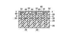
(i)次に、第三の金属膜76を全面に堆積し、リソグラフィ技術とエッチング技術を用いて、図45乃至図48に示す第三の配線78を形成する。この時、第三の配線78は、第二の金属膜74からなる第三のコンタクトと電気的に接続される。第三の配線78は、第二の金属膜74からなる第三のコンタクト70と、第二の配線68と、第二のコンタクト64とを介して、二本のNAND列に電気的に接続される。第三の配線78は、ビット線BLとなる。以上の工程を踏まえることで、図1(a)、図2(a)、図4および図9の回路構成図に示した通り、2列のNAND列で1本のビット線BLを共有し、ビット線BL自身とビット線BLとビット線BL側の選択ゲートトランジスタの拡散層を接続するビット線コンタクトCBをNAND列ピッチの2倍のピッチで配置することが可能である。(I) Next, a
図49乃至図68を用いて、本発明の実施例3に係る不揮発性半導体記憶装置として、NAND型EEPROMのメモリセル領域10、選択ゲートトランジスタ領域12、及びビット線BL形成の製造方法を平面パターン図、I−I方向断面図、II−II方向断面図、III−III方向断面図を用いて説明する。 49 to 68, as a nonvolatile semiconductor memory device according to
(a)図49乃至図52に示す構造は、実施例1の図25乃至図28に相当する。実施例1との違いは、2本の選択ゲートトランジスタの配線を共に、第二のゲート電極2の膜で形成することである。(A) The structure shown in FIGS. 49 to 52 corresponds to FIGS. 25 to 28 of the first embodiment. The difference from the first embodiment is that both the wirings of the two selection gate transistors are formed by the film of the
(b)次に、図53乃至図56に示すように、リソグラフィ技術とエッチング技術を用いて、第一の開口領域50内と第二の開口領域80内の第二の絶縁膜32を除去する。この時、第一の開口領域50、及び第二の開口領域80内の第三の絶縁膜40も同様に除去され、後述する金属サリサイド工程にて、第一の開口領域50、及び第二の開口領域80内の第三の絶縁膜40を介して隣接する第一のゲート電極8の膜と第二のゲート電極2の膜が、金属サリサイド膜49を介して電気的に接続可能となる。次に、全面に金属薄膜を形成して加熱を行い、第二の絶縁膜32と第四の絶縁膜48をサリサイド抑制膜として使用することにより、第二のゲート電極2の膜上面、第一の開口領域50、及び第二の開口領域80内の第一のゲート電極8の膜上面と露出したシリコン半導体基板26表面のみに金属サリサイド膜49を形成することが可能である(図53乃至図56)。(B) Next, as shown in FIGS. 53 to 56, the second insulating
(c)次に、層間絶縁膜として第五の絶縁膜52を全面に積層し、CMP技術や化学的ドライエッチング(CDE)技術を用いて平坦化し、リソグラフィ技術とエッチング技術を用いて、第二のコンタクト溝58を形成し、図57乃至図60に示す構造を形成する。(C) Next, a fifth insulating
(d)次に、全面に第一の金属膜60を堆積し、CMP技術を用いて、第五の絶縁膜52まで研磨し、図61乃至図64に示す第二のコンタクト64を形成する。この時、第二のコンタクト64は、第二のコンタクト64に接する選択ゲートトランジスタの拡散層に電気的に接続され、隣り合う二本のNAND列は、電気的に接続される。(D) Next, a
(e)次に、図65乃至図68に示すように、第三の金属膜76を全面に堆積し、リソグラフィ技術とエッチング技術を用いて、第三の金属膜76からなる第三の配線78を形成する。この時、第三の配線78は、第二のコンタクト64と電気的に接続される。第三の配線78は、第二のコンタクト64を介して、二本のNAND列に電気的に接続される。第三の配線78は、ビット線BLとなる。以上の工程を踏まえることで、図1(a)、図2(a)、図4および図9の回路構成図に示した通り、2列のNAND列で1本のビット線BLを共有し、ビット線BL自身とビット線BLとビット線BL側の選択ゲートトランジスタの拡散層を接続するビット線コンタクトCBをNAND列ピッチの2倍のピッチで配置することが可能である。特に、実施例3では、実施例2と比べ、第一の配線66及び第二の配線68と第三のコンタクト70を省略することが可能であり、製造プロセスが簡単になるという利点もある。(E) Next, as shown in FIGS. 65 to 68, a
図69乃至図92を用いて、本発明の実施例4に係る不揮発性半導体記憶装置として、NAND型EEPROMのメモリセル領域10、選択ゲートトランジスタ領域12、及びビット線形成の製造方法を平面パターン図、I−I方向断面図、II−II方向断面図、III−III方向断面図を用いて説明する。 69 to 92 are plan pattern diagrams showing a method of manufacturing a NAND type EEPROM
(a)図69乃至図72に示す構造は、実施例2の図25乃至図28、或いは実施例3の図49乃至図52に相当する。実施例2、或いは実施例3との違いは、2本の選択ゲートトランジスタの配線を共に、第一の配線66で形成することである。(A) The structure shown in FIGS. 69 to 72 corresponds to FIGS. 25 to 28 of the second embodiment or FIGS. 49 to 52 of the third embodiment. The difference from the second embodiment or the third embodiment is that both the wirings of the two selection gate transistors are formed by the
(b)次に、図73乃至図76に示すように、全面に金属薄膜を形成して加熱を行い、第二の絶縁膜32と第四の絶縁膜48をサリサイド抑制膜として使用することにより、第二のゲート電極2の膜上面と露出したシリコン半導体基板26表面のみに金属サリサイド膜49を形成することが可能である。(B) Next, as shown in FIGS. 73 to 76, a metal thin film is formed on the entire surface and heated, and the second insulating
(c)次に、層間絶縁膜として第五の絶縁膜52を全面に積層し、CMP技術やCDE技術を用いて平坦化し、第六の絶縁膜54を全面に積層する。その後、リソグラフィ技術とエッチング技術を用いて、第一のコンタクト溝56と第二のコンタクト溝58を形成し、図77乃至図80に示す構造を形成する。(C) Next, a fifth insulating
(d)次に、図81乃至図84に示すように、リソグラフィ技術とエッチング技術を用いて、第六の絶縁膜54のみを一部除去し、第一の配線溝と第二の配線溝を形成した後、全面に第一の金属膜60を堆積し、CMP技術を用いて、第六の絶縁膜54まで研磨し、第一のコンタクト62と第二のコンタクト64と第一の配線66と第二の配線68を形成する。この時、第一のコンタクト62に接する隣り合うフローティングゲート8は、第一のコンタクト62を介して電気的に接続される。第一のコンタクト62と第一の配線66は、電気的に接続される。第二のコンタクト64は、第二のコンタクト64に接する選択ゲートトランジスタの拡散層に電気的に接続される。その結果、隣り合う二本のNAND列は、電気的に接続され、第二のコンタクト64と第二の配線68は、電気的に接続される。(D) Next, as shown in FIGS. 81 to 84, only the sixth insulating
(e)次に、図85乃至図88に示すように、層間絶縁膜となる第七の絶縁膜72を全面に堆積後、リソグラフィ技術とエッチング技術を用いて、第三のコンタクト溝を形成し、第二の金属膜74を堆積し、CMP技術を用いて、第七の絶縁膜72まで研磨し、第二の金属膜74からなる第三のコンタクト82を形成する。この時、第三のコンタクト82は、第二の配線68に電気的に接続される。(E) Next, as shown in FIGS. 85 to 88, after depositing a seventh insulating
(f)次に、図89乃至図92に示すように、第三の金属膜76を全面に堆積し、リソグラフィ技術とエッチング技術を用いて、第三の金属膜76からなる第三の配線78を形成する。この時、第三の配線78は、第三のコンタクト82と電気的に接続される。第三の配線78は、第三のコンタクト82と第二の配線68と第二のコンタクト64を介して、二本のNAND列に電気的に接続される。その結果、第三の配線78は、ビット線BLとなる。(F) Next, as shown in FIGS. 89 to 92, a
以上の工程を踏まえることで、図1(a)、図2(a)、図4および図9の回路構成図に示した通り、2列のNAND列で1本のビット線BLを共有し、ビット線BL自身とビット線BLとビット線BL側の選択ゲートトランジスタの拡散層を接続するビット線コンタクトCBをNAND列ピッチの2倍のピッチで配置することが可能である。実施例2と比較して、図29に示す第一の開口領域50を形成する工程が省略可能であり、製造プロセスが簡単になるという利点もある。 Based on the above processes, as shown in the circuit configuration diagrams of FIGS. 1A, 2A, 4 and 9, one bit line BL is shared by two NAND columns, It is possible to arrange the bit line contacts CB connecting the bit lines BL themselves, the bit lines BL, and the diffusion layers of the selection gate transistors on the bit line BL side, with a pitch twice the NAND column pitch. Compared with the second embodiment, the step of forming the
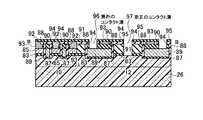
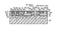
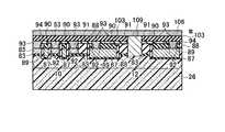
図93乃至図140を用いて、本発明の実施例5に係る不揮発性半導体記憶装置として、NAND型EEPROMのメモリセル領域10、選択ゲートトランジスタ領域12、及びビット線形成の製造方法を平面パターン図、I−I方向断面図、II−II方向断面図、III−III方向断面図を用いて説明する。 93 to 140 are plan pattern diagrams showing a method of manufacturing a NAND type EEPROM
(a)まず、シリコン半導体基板26上にメモリセルトランジスタのゲート絶縁膜となる第八の絶縁膜83、コントロールゲートとなる第三のゲート電極85の膜と第九の絶縁膜84を全面に積層する。第九の絶縁膜84の選択には、第三のゲート電極85とエッチング選択比が得られることが最低条件であるが、後述する素子分離領域28用絶縁膜と、第四のゲート電極89とのCMP工程における研磨選択比が得られる絶縁膜であることがより望ましい。その後、リソグラフィ技術とエッチング技術を用いて素子分離溝を形成し、素子分離領域28用絶縁膜を全面に堆積した後、CMP技術を用いて、素子分離領域28を形成する。その後、リソグラフィ技術とエッチング技術を用いて、フローティングゲート89の形成予定部分を形成する(図93乃至図96)。この時、フローティングゲート89の形成予定部分は適切な深さまでシリコン半導体基板26のエッチングが行われ、素子分離領域28は選択エッチングにより埋め込み絶縁膜がほとんどエッチングされないことが望ましい。(A) First, an eighth insulating
(b)次に、適当な熱処理を行った後、コントロールゲート85とフローティングゲート89間の層間絶縁膜となる第十の絶縁膜86を堆積し、メモリセルトランジスタのチャネルプロファイルの形成、トンネル絶縁膜として機能する第十一の絶縁膜87形成部の開口を行う。メモリセル形成領域のウェル内の不純物プロファイルと掘り込み深さでメモリセルトランジスタのしきい値を調整することにより、チャネルプロファイルの形成工程を省略することももちろん可能である。次に、メモリセルトランジスタのトンネル酸化膜となる第十一の絶縁膜87を形成し、図97乃至図100に示す構造を形成する。(B) Next, after performing an appropriate heat treatment, a tenth insulating
(c)次に、フローティングゲート89となる第四のゲート電極89の膜を全面に積層し、エッチバック技術を用いて、フローティングゲート89の高さを下げ、図101乃至図104に示す構造を形成する。図101乃至図104に示すコントロールゲート85の上面は、後述のCMP工程において形成されるフローティングゲート89上面から、適切な絶縁耐性が得られる距離まで離れた位置に制御されることが望ましい。このとき、コントロールゲート85高さの制御性を高めるため、第十の絶縁膜87をマスク材としてCMP技術により第四の電極89の膜を平坦化した後、上記エッチングを行うことも可能である。(C) Next, a film of the
(d)次に、コントロールゲート85を絶縁するために第十二の絶縁膜90を全面に形成した後、CMP技術を用いて、第三のゲート電極85のみを露出させ、図105乃至図108に示す構造を形成する。この時、第十二の絶縁膜90は、第三のゲート電極85とエッチング選択比が得られることが最低条件である。(D) Next, after a twelfth insulating
(e)次に、選択ゲートトランジスタを形成する工程の一つとして、リソグラフィ技術とエッチング技術を用いて、第三のゲート電極85を選択エッチングした後、第十三の絶縁膜91を全面に堆積後、CMP技術を用いて、第三のゲート電極85のみを露出させ、図109乃至図112に示す構造を形成する。(E) Next, as one of the steps of forming the select gate transistor, the
(f)次に、リソグラフィ技術とエッチング技術を用いて、図113に示す第三の開口領域110内の第十二の絶縁膜90を選択エッチングし、第四のゲート電極89を露出させ、図113乃至図116に示す構造を形成する。(F) Next, using a lithography technique and an etching technique, the twelfth insulating
(g)次に、エッチング技術を用いて第三のゲート電極85の膜上面の高さを下げ、第十四の絶縁膜92を全面形成した後、エッチング技術を用いて、フローティングゲート89上面に制御ゲート幅より狭い開口部を形成し、図117乃至図120に示す構造を形成する。ここで形成する第十四の絶縁膜92は、隣接するコントロールゲート85との耐圧を十分確保するために適切な膜厚に設定されることが望ましい。(G) Next, the height of the upper surface of the
(h)次に、金属膜を全面に堆積後、リソグラフィ技術とエッチング技術を用いて、コントロールゲートとして機能する第三のゲート電極85の膜と金属膜を電気的に接続させ、ワード線であり、選択ゲートトランジスタのゲート配線となる第四の配線93を形成し、層間絶縁膜となる第十五の絶縁膜94を堆積し、図121乃至図124に示す構造を形成する。その手法は、例えば金属膜を全面形成した後に選択エッチングにより第四の配線93を形成する方法、または、絶縁膜を形成した後に溝を掘って金属を埋め込み、CMPによって第四の配線93を形成する方法、など通常の配線を形成する手法ならばいずれを用いても形成可能である。これらの配線を形成するためのリソグラフィ時に合せズレが発生するが、上記コントロールゲート85上面に自己整合的に設けた開口部により、隣接ワード線間での耐圧は十分に確保することが可能である。また、コントロールゲート85と上記第四の配線93の配線材との接触抵抗を低減するため、第四の配線93形成前にサリサイド工程を行うことももちろん可能である。(H) Next, after a metal film is deposited on the entire surface, the film of the
(i)次に、第十六の絶縁膜95を全面に堆積した後、リソグラフィ技術とエッチング技術を用いて、第四のコンタクト溝96と第五のコンタクト溝97を形成し、図125乃至図128に示す構造を形成する。(I) Next, after depositing a sixteenth insulating
(j)次に、リソグラフィ技術とエッチング技術を用いて、第十六の絶縁膜95のみを一部除去し、第五の配線溝と第六の配線溝を形成した後、全面に金属膜を堆積し、CMP技術を用いて、第十六の絶縁膜95まで研磨し、図129乃至図132に示す第四のコンタクト101と第五のコンタクト102と第五の配線99と第六の配線100を形成する。この時、第四のコンタクト101に接する隣り合う第四のゲート電極89は、第四のコンタクト101を介して電気的に接続される。第四の配線93は選択ゲートトランジスタのゲート配線となる。第五のコンタクト102は、第五のコンタクト102に接する選択ゲートトランジスタの拡散層に電気的に接続される。その結果、隣り合う二本のNAND列は、電気的に接続され、第五のコンタクト102と第六の配線100は、電気的に接続される。この時、第五のコンタクト102と第五の配線99と、第四のコンタクト101と第六の配線100とは、電気的に独立である。(J) Next, only a part of the sixteenth insulating
(k)次に、層間絶縁膜となる第十七の絶縁膜103を全面に堆積後、リソグラフィ技術とエッチング技術を用いて、第六のコンタクト溝を形成し、金属膜を堆積し、CMP技術を用いて、第十七の絶縁膜103まで研磨し、図133乃至図136に示す第六のコンタクト104を形成する。この時、第六のコンタクト104は、第六の配線100に電気的に接続される。(K) Next, after depositing an seventeenth
(l)次に、金属膜を全面に堆積し、リソグラフィ技術とエッチング技術を用いて、図137乃至図140に示す第七の配線106を形成する。この時、第七の配線106は、第六のコンタクト104と電気的に接続される。第七の配線106は、第六のコンタクト104と第六の配線100と第五のコンタクト102を介して、二本のNAND列に電気的に接続される。その結果、第七の配線106は、ビット線BLとなる。(L) Next, a metal film is deposited on the entire surface, and the
以上の工程を踏まえることで2列のNAND列で1本のビット線BLを共有し、ビット線BLとビット線BL側の選択ゲートトランジスタの拡散層とを接続するビット線コンタクトCBをNAND列ピッチの倍のピッチで配置することが可能である。 Based on the above process, the bit line contact CB that shares one bit line BL in the two NAND columns and connects the bit line BL and the diffusion layer of the selection gate transistor on the bit line BL side is arranged in the NAND column pitch. It is possible to arrange them at a pitch twice that of.
図141乃至図145を用いて、本発明の実施例6に係る不揮発性半導体記憶装置として、NAND型EEPROMのメモリセル領域10、選択ゲートトランジスタ領域12、及びビット線形成の製造方法を平面パターン図、I−I方向断面図、II−II方向断面図、III−III方向断面図を用いて説明する。 FIG. 141 to FIG. 145 are plan pattern diagrams showing a manufacturing method for forming a
(a)図141に示す構造は、実施例5の図113乃至図116に相当する。実施例5との違いは、第三の開口領域110、第四の開口領域120を設け、第四の配線93にて第一、第二の選択ゲートトランジスタのゲート配線とすることである。(A) The structure shown in FIG. 141 corresponds to FIGS. 113 to 116 of the fifth embodiment. The difference from the fifth embodiment is that the
(b)図142乃至図145に実施例5の図137乃至図140に相当する構造を示す。実施例2と実施例3の違いと同様、第五の配線99、及び第六の配線100と第四のコンタクト101、及び第五のコンタクト102を省略することが可能である。(B) FIGS. 142 to 145 show structures corresponding to FIGS. 137 to 140 of the fifth embodiment. Similarly to the difference between the second embodiment and the third embodiment, the
図146乃至図150を用いて、本発明の実施例7に係る不揮発性半導体記憶装置として、NAND型EEPROMのメモリセル領域10、選択ゲートトランジスタ領域12、及びビット線形成の製造方法を平面パターン図、I−I方向断面図、II−II方向断面図、III−III方向断面図を用いて説明する。 FIG. 146 to FIG. 150 are plan pattern diagrams showing a manufacturing method of forming a NAND type EEPROM
(a)図146に示す構造は、実施例5の図125乃至図128に相当する。実施例5、或いは実施例6との違いは、第三の開口領域110、或いは第四の開口領域120を設ける必要が無く、第五の配線99にて第一、第二の選択ゲートトランジスタのゲート配線とすることである。(A) The structure shown in FIG. 146 corresponds to FIGS. 125 to 128 of the fifth embodiment. The difference from the fifth embodiment or the sixth embodiment is that there is no need to provide the
(b)図147乃至図150に実施例5の図137乃至図140に相当する構造を示す。実施例2と実施例3の違いと同様、第三の開口領域110、或いは第四の開口領域120を形成する工程が省略可能である。(B) FIGS. 147 to 150 show structures corresponding to FIGS. 137 to 140 of the fifth embodiment. Similar to the difference between the second embodiment and the third embodiment, the step of forming the
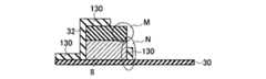
図151乃至図154を用いて、本発明の実施例8に係る不揮発性半導体記憶装置として、NAND型EEPROMの特に選択ゲートトランジスタ領域12の製造方法を部分的な断面構造図を用いて説明する。図151乃至図154は上記実施例2および実施例3に関係しており、特にコントロールゲート2とフローティングゲート8近傍における拡大断面構造図となっている。側壁部分の一部のゲート間絶縁膜130を剥離して直接フローティングゲート8とコントロールゲート2とを電気的に接触させる構造を有する点に特徴がある。尚、図151乃至図154においては、シリコン半導体基板よりも上の部分の拡大図であって、シリコン半導体基板については省略している。 With reference to FIGS. 151 to 154, as a nonvolatile semiconductor memory device according to
(a)フローティングゲート或いは選択ゲートトランジスタのゲート電極となる第一のゲート電極8の膜をリソグラフィーとエッチングによって加工した直後の断面構造は、図151に示すように、トンネル酸化膜によって形成された第一の絶縁膜30と、第一のゲート電極8と、第二の絶縁膜32を備える。(A) The cross-sectional structure immediately after processing the film of the
(b)次に、第一のゲート電極8とコントロールゲート2の間のゲート間絶縁膜130を全面に堆積した直後の断面構造は、図152に示すように、図151における側壁部分にもほぼ均一にゲート間絶縁膜130が堆積されている。(B) Next, as shown in FIG. 152, the cross-sectional structure immediately after the inter-gate
(c)次に、上記ゲート間絶縁膜130を第一のゲート電極8の側面において、リソグラフィーとエッチングにより剥離した直後の断面構造は、図153の部分Mに示すように、ゲート間絶縁膜130剥離時に第一のゲート電極8上のゲート間絶縁膜130も一部除去されていても良い。或はまた、図153の部分Nに示すように、剥離部分は第一のゲート電極8の側面の一部であっても良い。或いはまた、剥離部分は第一のゲート電極8の側面の全部であっても良い。第一のゲート電極8と、選択ゲートトランジスタの選択ゲート配線(SG)となるコントロールゲート(CG)2とが電気的に接続され得る構造が実現されていれば良い。(C) Next, the cross-sectional structure immediately after the
(d)次に、コントロールゲート(CG)および選択ゲートトランジスタのゲート配線(SG)となるゲート電極膜を全面に堆積した後、図154に示すように、第一のゲート電極8とコントロールゲート(CG)2および選択ゲートトランジスタの選択ゲート配線(SG)となるゲート電極膜とを電気的に接触させる。その後の工程は、実施例2および実施例3と同様である。但し、第一のゲート電極8上面のマスク材を剥離する工程は必要ない。(D) Next, after depositing a gate electrode film to be the control gate (CG) and the gate wiring (SG) of the selection gate transistor over the entire surface, as shown in FIG. 154, the
本発明の実施例1乃至実施例8に係る不揮発性半導体記憶装置における応用例を本発明の実施例9として図155に示す。図155は、本発明によるフラッシュメモリ装置及びシステムの主要構成要素の概略的なブロック図である。図に示すように、フラッシュメモリシステム142はホストプラットホーム144、及びユニバーサル・シリアル・バス(USB)フラッシュ装置146より構成される。 FIG. 155 shows an application example of the nonvolatile semiconductor memory device according to the first to eighth embodiments of the present invention as the ninth embodiment of the present invention. FIG. 155 is a schematic block diagram of the main components of the flash memory device and system according to the present invention. As shown in the figure, the flash memory system 142 includes a
ホストプラットホーム144は、USBケーブル148を介して、本発明によるUSBフラッシュ装置146へ接続されている。ホストプラットホーム144は、USBホストコネクタ150を介してUSBケーブル148に接続し、USBフラッシュ装置146はUSBフラッシュ装置コネクタ152を介してUSBケーブル148に接続する。ホストプラットホーム144は、USBバス上のパケット伝送を制御するUSBホスト制御器154を有する。 The
USBフラッシュ装置146は、USBフラッシュ装置146の他の要素を制御し、かつUSBフラッシュ装置146のUSBバスへのインタフェースを制御するUSBフラッシュ装置制御器156と、USBフラッシュ装置コネクタ152と、本発明の実施例1乃至実施例8に係る不揮発性半導体記憶装置で構成された少なくとも一つのフラッシュメモリモジュール158を含む。 The
USBフラッシュ装置146がホストプラットホーム144に接続されると、標準USB列挙処理が始まる。この処理において、ホストプラットホーム144は、USBフラッシュ装置146を認知してUSBフラッシュ装置146との通信モードを選択し、エンドポイントという、転送データを格納するFIFOバッファを介して、USBフラッシュ装置146との間でデータの送受信を行う。ホストプラットホーム144は、他のエンドポイントを介してUSBフラッシュ装置146の脱着等の物理的、電気的状態の変化を認識し、受け取るべきパケットがあれば、それを受け取る。 When the
ホストプラットホーム144は、USBホスト制御器154へ要求パケットを送ることによって、USBフラッシュ装置146からのサービスを求める。USBホスト制御器154は、USBケーブル148上にパケットを送信する。USBフラッシュ装置146がこの要求パケットを受け入れたエンドポイントを有する装置であれば、これらの要求はUSBフラッシュ装置制御器156によって受け取られる。 The
次に、USBフラッシュ装置制御器156は、フラッシュメモリモジュール158から、あるいはフラッシュメモリモジュール158へ、データの読み出し、書き込み、あるいは消去等の種々の操作を行う。それとともに、USBアドレスの取得等の基本的なUSB機能をサポートする。USBフラッシュ装置制御器156は、フラッシュメモリモジュール158の出力を制御する制御ライン160を介して、また、例えば、/CE等の種々の他の信号や読み取り書き込み信号を介して、フラッシュメモリモジュール158を制御する。また、フラッシュメモリモジュール158は、アドレスデータバス162によってもUSBフラッシュ装置制御器156に接続されている。アドレスデータバス162は、フラッシュメモリモジュール158に対する読み出し、書き込みあるいは消去のコマンドと、フラッシュメモリモジュール158のアドレス及びデータを転送する。 Next, the USB
ホストプラットホーム144が要求した種々の操作に対する結果及び状態に関してホストプラットホーム144へ知らせるために、USBフラッシュ装置146は、状態エンドポイント(エンドポイント0)を用いて状態パケットを送信する。この処理において、ホストプラットホーム144は、状態パケットがないかをチェックし(ポーリング)、USBフラッシュ装置146は、新しい状態メッセージのパケットが存在しない場合に空パケットを、あるいは状態パケットそのものを返す。 In order to inform the
以上、USBフラッシュ装置の様々な機能を実現可能である。上記USBケーブルを省略し、コネクタ間を直接接続することも可能である。 As described above, various functions of the USB flash device can be realized. It is also possible to omit the USB cable and connect the connectors directly.
上記のように、本発明は実施例によって記載したが、この開示の一部をなす論述及び図面はこの発明を限定するものであると理解すべきではない。この開示から当業者には様々な代替実施例及び運用技術が明らかとなろう。したがって、本発明の技術範囲は上記の説明から妥当な特許請求の範囲に係る発明特定事項によってのみ定められるものである。 Although the present invention has been described by way of example as described above, it should not be understood that the discussion and drawings that form part of this disclosure limit the present invention. From this disclosure, various alternative embodiments and operational techniques will be apparent to those skilled in the art. Therefore, the technical scope of the present invention is defined only by the invention specifying matters according to the scope of claims reasonable from the above description.
その他、本発明の要旨を逸脱しない範囲で、様々に変形して実施することができる。なお、上記各実施例は、それぞれ組み合わせて実施することができる。このように、本発明はここでは記載していない様々な実施例等を含むことは勿論である。 In addition, various modifications can be made without departing from the scope of the present invention. In addition, each said Example can be implemented in combination, respectively. As described above, the present invention naturally includes various embodiments that are not described herein.
本発明の不揮発性半導体記憶装置によれば、2列のNAND列で1本のビット線BLを共有し、NAND型EEPROMの高集積化を可能にすることから、メモリカード、ICカードのみならず、車載用システム、ハードディスクドライバ、携帯電話、高速ネットワーク用モデム機器等幅広い産業上の利用可能性が存在する。 According to the nonvolatile semiconductor memory device of the present invention, since one bit line BL is shared by two NAND columns and high integration of the NAND type EEPROM is enabled, not only a memory card and an IC card are used. There is a wide range of industrial applicability, such as in-vehicle systems, hard disk drivers, mobile phones, and high-speed network modem devices.
1…ビット線駆動回路
2…コントロールゲート(第二のゲート電極)
4,6…選択ゲート
8…フローティングゲート(第一のゲート電極)
10…メモリセル領域
12…選択ゲートトランジスタ領域
18…拡散層
20…制御ゲート線駆動回路
21…選択ゲート線駆動回路
22…ソース線駆動回路
23…2本の制御ゲート線に挟まれる全メモリセルトランジスタ
24…NANDメモリセルアレイ
24a〜24f…NANDメモリセルユニット
26…pウェル又はシリコン半導体基板
28…素子分離領域
30…第一の絶縁膜
32…第二の絶縁膜
40…第三の絶縁膜
46…側壁絶縁膜
48…第四の絶縁膜
49…金属サリサイド膜
50…第一の開口領域
52…第五の絶縁膜
54…第六の絶縁膜
56…第一のコンタクト溝
58…第二のコンタクト溝
60…第一の金属膜
62…第一のコンタクト
64…第二のコンタクト
66…第一の配線
68…第二の配線
70,82…第三のコンタクト
72…第七の絶縁膜
74…第二の金属膜
76…第三の金属膜
78…第三の配線(BL)
80…第二の開口領域
83…第八の絶縁膜
84…第九の絶縁膜
85…コントロールゲート(第三のゲート電極)
86,88…第十の絶縁膜(側壁絶縁膜)
87…第十一の絶縁膜
89…フローティングゲート(第四のゲート電極)
90…第十二の絶縁膜
91…第十三の絶縁膜
92…第十四の絶縁膜
93…第四の配線
94…第十五の絶縁膜
95…第十六の絶縁膜
99…第五の配線
100…第六の配線
101…第四のコンタクト
102…第五のコンタクト
103…第十七の絶縁膜
104…第六のコンタクト
106…第七の配線
108…第八の配線
109…第八のコンタクト
110…第三の開口領域
120…第四の開口領域
130…ゲート間絶縁膜
144…ホストプラットホーム
146…USBフラッシュ装置
148…USBケーブル
150,152…USBコネクタ
154…USBホスト制御器
158…フラッシュメモリモジュール
160…制御ライン
162…アドレスデータバス
BL,BLk,BLk−1,BLk+1…ビット線
SG01,SG02,SG03,SG04,SGD1,SGD2,SGS…選択ゲート線
CG0,CG1,CG2,…,CG8,…,CG17,WL…制御ゲート線(コントロールゲート線)
SG1,SG2,SG3,SG4…選択ゲートトランジスタ
MC,MC1.k,MC2.k,…,MC8.k,MC1.k+1,MC2.k+1,…,MC8.k+1…メモリセル
CB…ビット線コンタクト
CS…ソース線コンタクト
Vdd…電源電圧
Vbl,VBLpgm,VBLinhibit…ビット線に与える電圧
Vread…読み出し電圧
Vsg,Vsgd…選択ゲートトランジスタに与える電圧
Vth(SG)…選択ゲートトランジスタの閾値電圧
Vpgm…書き込み電圧
Vpass…中間電圧
A〜N…表示DESCRIPTION OF
4, 6 ...
DESCRIPTION OF
80 ...
86, 88 ... Tenth insulating film (side wall insulating film)
87 ... Eleventh insulating
90 ... Twelfth insulating
SG1, SG2, SG3, SG4... Select gate transistors MC, MC1. k, MC2. k, ..., MC8. k, MC1. k + 1, MC2. k + 1,..., MC8. k + 1... memory cell CB... bit line contact CS... source line contact Vdd... power supply voltage Vbl, VBLpgm, VBLinhibit. Transistor threshold voltage Vpgm ... write voltage Vpass ... intermediate voltages A to N ... display
Claims (27)
Translated fromJapanese前記第一のメモリセル列とビット線との間に接続された第一の選択ゲートトランジスタと、
前記第二のメモリセル列と前記ビット線との間に接続された第二の選択ゲートトランジスタ
とを備え、前記ビット線と前記第一および第二の選択ゲートトランジスタの拡散層とを接続するビット線コンタクトを前記メモリセル列ピッチの2倍のピッチで配置することを特徴とする不揮発性半導体記憶装置。A first and second memory cell array in which a plurality of memory cell transistors each having a gate structure with first and second control gates arranged on both sides of the floating gate are connected in series;
A first select gate transistor connected between the first memory cell column and a bit line;
A second select gate transistor connected between the second memory cell column and the bit line, the bit connecting the bit line and the diffusion layers of the first and second select gate transistors A non-volatile semiconductor memory device, wherein line contacts are arranged at a pitch twice as large as the memory cell column pitch.
前記第二のメモリセル列と前記ソース線との間に接続された第四の選択ゲートトランジスタ
とを更に備えることを特徴とする請求項1記載の不揮発性半導体記憶装置。A third select gate transistor connected between the first memory cell column and a source line;
The nonvolatile semiconductor memory device according to claim 1, further comprising a fourth select gate transistor connected between the second memory cell column and the source line.
前記第一の選択ゲートトランジスタのゲートに接続され、前記複数のコントロールゲート線に平行に配列された第一の選択ゲート線と、
前記第二の選択ゲートトランジスタのゲートに接続され、前記複数のコントロールゲート線に平行に配列された第二の選択ゲート線と、
前記第三の選択ゲートトランジスタのゲートに接続され、前記複数のコントロールゲート線に平行に配列された第三の選択ゲート線
とを更に備えることを特徴とする請求項2記載の不揮発性半導体記憶装置。A plurality of control gate lines connected to the first and second control gates and orthogonal to the bit lines;
A first selection gate line connected to the gate of the first selection gate transistor and arranged in parallel to the plurality of control gate lines;
A second selection gate line connected to the gate of the second selection gate transistor and arranged parallel to the plurality of control gate lines;
3. The nonvolatile semiconductor memory device according to claim 2, further comprising: a third selection gate line connected to a gate of the third selection gate transistor and arranged parallel to the plurality of control gate lines. .
前記第一の選択ゲートトランジスタのゲートに接続され、前記複数のコントロールゲート線に平行に配列された第一の選択ゲート線と、
前記第二の選択ゲートトランジスタのゲートに接続され、前記複数のコントロールゲート線に平行に配列された第二の選択ゲート線と、
前記第三の選択ゲートトランジスタのゲートに接続され、前記複数のコントロールゲート線に平行に配列された第三の選択ゲート線と、
前記第四の選択ゲートトランジスタのゲートに接続され、前記複数のコントロールゲート線に平行に配列された第四の選択ゲート線
とを更に備えることを特徴とする請求項3記載の不揮発性半導体記憶装置。A plurality of control gate lines connected to the first and second control gates of the memory cell and orthogonal to the bit lines;
A first selection gate line connected to the gate of the first selection gate transistor and arranged in parallel to the plurality of control gate lines;
A second selection gate line connected to the gate of the second selection gate transistor and arranged parallel to the plurality of control gate lines;
A third selection gate line connected to the gate of the third selection gate transistor and arranged parallel to the plurality of control gate lines;
4. The nonvolatile semiconductor memory device according to claim 3, further comprising: a fourth selection gate line connected to a gate of the fourth selection gate transistor and arranged in parallel with the plurality of control gate lines. .
前記コントロールゲート線に接続されるコントロールゲート線駆動回路と、
前記選択ゲート線に接続される選択ゲート線駆動回路と、
前記ソース線に接続されるソース線駆動回路
とを更に備えることを特徴とする請求項2〜5のいずれか1項に記載の不揮発性半導体記憶装置。A bit line driving circuit connected to the bit line;
A control gate line driving circuit connected to the control gate line;
A selection gate line driving circuit connected to the selection gate line;
The nonvolatile semiconductor memory device according to claim 2, further comprising: a source line driving circuit connected to the source line.
前記フローティングゲートの両側に対応する前記半導体基板内に形成され、前記メモリセルトランジスタのソース又はドレインとなる拡散層と、
前記二つの拡散層に面する前記第一、第二のコントロールゲートと前記フローティングゲートとの間の二つの側壁に形成されるゲート間絶縁膜
とを更に備えることを特徴とする請求項1記載の不揮発性半導体記憶装置。A gate insulating film formed between a semiconductor substrate and the floating gate;
A diffusion layer formed in the semiconductor substrate corresponding to both sides of the floating gate and serving as a source or drain of the memory cell transistor;
The inter-gate insulating film formed on two sidewalls between the first and second control gates facing the two diffusion layers and the floating gate, further comprising: Nonvolatile semiconductor memory device.
前記第二のメモリセル列と前記ソース線との間に接続された第四の選択ゲートトランジスタ
とを更に備えることを特徴とする請求項7記載の不揮発性半導体記憶装置。A third select gate transistor connected between the first memory cell column and a source line;
The nonvolatile semiconductor memory device according to claim 7, further comprising a fourth select gate transistor connected between the second memory cell column and the source line.
前記第一の選択ゲートトランジスタのゲートに接続され、前記複数のコントロールゲート線に平行に配列された第一の選択ゲート線と、
前記第二の選択ゲートトランジスタのゲートに接続され、前記複数のコントロールゲート線に平行に配列された第二の選択ゲート線と、
前記第三の選択ゲートトランジスタのゲートに接続され、前記複数のコントロールゲート線に平行に配列された第三の選択ゲート線
とを更に備えることを特徴とする請求項8記載の不揮発性半導体記憶装置。A plurality of control gate lines connected to the first and second control gates of the memory cell and orthogonal to the bit lines;
A first selection gate line connected to the gate of the first selection gate transistor and arranged in parallel to the plurality of control gate lines;
A second selection gate line connected to the gate of the second selection gate transistor and arranged parallel to the plurality of control gate lines;
9. The nonvolatile semiconductor memory device according to claim 8, further comprising: a third selection gate line connected to a gate of the third selection gate transistor and arranged in parallel with the plurality of control gate lines. .
前記第一の選択ゲートトランジスタのゲートに接続され、前記複数のコントロールゲート線に平行に配列された第一の選択ゲート線と、
前記第二の選択ゲートトランジスタのゲートに接続され、前記複数のコントロールゲート線に平行に配列された第二の選択ゲート線と、
前記第三の選択ゲートトランジスタのゲートに接続され、前記複数のコントロールゲート線に平行に配列された第三の選択ゲート線と、
前記第四の選択ゲートトランジスタのゲートに接続され、前記複数のコントロールゲート線に平行に配列された第四の選択ゲート線
とを更に備えることを特徴とする請求項9記載の不揮発性半導体記憶装置。A plurality of control gate lines connected to the first and second control gates of the memory cell and orthogonal to the bit lines;
A first selection gate line connected to the gate of the first selection gate transistor and arranged in parallel to the plurality of control gate lines;
A second selection gate line connected to the gate of the second selection gate transistor and arranged parallel to the plurality of control gate lines;
A third selection gate line connected to the gate of the third selection gate transistor and arranged parallel to the plurality of control gate lines;
10. The nonvolatile semiconductor memory device according to claim 9, further comprising: a fourth selection gate line connected to a gate of the fourth selection gate transistor and arranged in parallel with the plurality of control gate lines. .
前記コントロールゲート線に接続されるコントロールゲート線駆動回路と、
前記選択ゲート線に接続される選択ゲート線駆動回路と、
前記ソース線に接続されるソース線駆動回路
とを更に備えることを特徴とする請求項8〜11のいずれか1項に記載の不揮発性半導体記憶装置。A bit line driving circuit connected to the bit line;
A control gate line driving circuit connected to the control gate line;
A selection gate line driving circuit connected to the selection gate line;
The nonvolatile semiconductor memory device according to claim 8, further comprising: a source line driving circuit connected to the source line.
前記フローティングゲートと前記溝の底部との間に形成された第八のゲート絶縁膜と、
前記フローティングゲートの両側に対応する前記半導体基板内に形成され、前記メモリセルトランジスタのソース又はドレインとなる拡散層と、
前記拡散層上に位置し,前記フローティングゲートを駆動する第一、第二のコントロールゲートと前記フローティングゲートとの間の両側壁に形成されたゲート間絶縁膜
とを更に備えることを特徴とする請求項1記載の不揮発性半導体記憶装置。A groove formed in a semiconductor substrate;
An eighth gate insulating film formed between the floating gate and the bottom of the trench;
A diffusion layer formed in the semiconductor substrate corresponding to both sides of the floating gate and serving as a source or drain of the memory cell transistor;
The semiconductor device further comprises an inter-gate insulating film formed on both side walls between the first and second control gates that are located on the diffusion layer and drives the floating gate, and between the floating gates. Item 12. A nonvolatile semiconductor memory device according to Item 1.
前記第二のメモリセル列と前記ソース線との間に接続された第四の選択ゲートトランジスタ
とを更に備えることを特徴とする請求項13記載の不揮発性半導体記憶装置。A third select gate transistor connected between the first memory cell column and a source line;
The nonvolatile semiconductor memory device according to claim 13, further comprising a fourth select gate transistor connected between the second memory cell column and the source line.
前記第一の選択ゲートトランジスタのゲートに接続され、前記複数のコントロールゲート線に平行に配列された第一の選択ゲート線と、
前記第二の選択ゲートトランジスタのゲートに接続され、前記複数のコントロールゲート線に平行に配列された第二の選択ゲート線と、
前記第三の選択ゲートトランジスタのゲートに接続され、前記複数のコントロールゲート線に平行に配列された第三の選択ゲート線
とを更に備えることを特徴とする請求項14記載の不揮発性半導体記憶装置。A plurality of control gate lines connected to the first and second control gates of the memory cell and orthogonal to the bit lines;
A first selection gate line connected to the gate of the first selection gate transistor and arranged in parallel to the plurality of control gate lines;
A second selection gate line connected to the gate of the second selection gate transistor and arranged parallel to the plurality of control gate lines;
15. The nonvolatile semiconductor memory device according to claim 14, further comprising a third selection gate line connected to the gate of the third selection gate transistor and arranged in parallel with the plurality of control gate lines. .
前記第一の選択ゲートトランジスタのゲートに接続され、前記複数のコントロールゲート線に平行に配列された第一の選択ゲート線と、
前記第二の選択ゲートトランジスタのゲートに接続され、前記複数のコントロールゲート線に平行に配列された第二の選択ゲート線と、
前記第三の選択ゲートトランジスタのゲートに接続され、前記複数のコントロールゲート線に平行に配列された第三の選択ゲート線と、
前記第四の選択ゲートトランジスタのゲートに接続され、前記複数のコントロールゲート線に平行に配列された第四の選択ゲート線
とを更に備えることを特徴とする請求項15記載の不揮発性半導体記憶装置。A plurality of control gate lines connected to the first and second control gates of the memory cell and orthogonal to the bit lines;
A first selection gate line connected to the gate of the first selection gate transistor and arranged in parallel to the plurality of control gate lines;
A second selection gate line connected to the gate of the second selection gate transistor and arranged parallel to the plurality of control gate lines;
A third selection gate line connected to the gate of the third selection gate transistor and arranged parallel to the plurality of control gate lines;
16. The nonvolatile semiconductor memory device according to claim 15, further comprising: a fourth selection gate line connected to the gate of the fourth selection gate transistor and arranged in parallel with the plurality of control gate lines. .
前記コントロールゲート線に接続されるコントロールゲート線駆動回路と、
前記選択ゲート線に接続される選択ゲート線駆動回路と、
前記ソース線に接続されるソース線駆動回路
とを更に備えることを特徴とする請求項14〜17のいずれか1項に記載の不揮発性半導体記憶装置。A bit line driving circuit connected to the bit line;
A control gate line driving circuit connected to the control gate line;
A selection gate line driving circuit connected to the selection gate line;
The nonvolatile semiconductor memory device according to claim 14, further comprising: a source line driving circuit connected to the source line.
前記メモリセルトランジスタのフローティングゲートおよび前記選択ゲートトランジスタのゲート電極となる第一のゲート電極を形成し、更に第二の絶縁膜を形成する工程と、
素子分離領域を形成後、前記メモリセルトランジスタのフローティングゲートとコントロールゲートの層間絶縁膜となる第三の絶縁膜を堆積し、前記メモリセルトランジスタのコントロールゲートと前記選択ゲートトランジスタのゲート配線となる第二のゲート電極を形成する工程と、
第四の絶縁膜を全面に積層形成し、前記第二のゲート電極上と露出した前記半導体基板表面上の前記第四の絶縁膜を除去する工程
とを備えることを特徴とする不揮発性半導体記憶装置の製造方法。Forming a first insulating film to be a gate insulating film of a memory cell transistor and a select gate transistor on a semiconductor substrate;
Forming a first gate electrode to be a floating gate of the memory cell transistor and a gate electrode of the selection gate transistor, and further forming a second insulating film;
After forming the element isolation region, a third insulating film serving as an interlayer insulating film between the floating gate and the control gate of the memory cell transistor is deposited, and a gate wiring for the control gate of the memory cell transistor and the gate wiring of the selection gate transistor is formed. Forming a second gate electrode;
And a step of forming a fourth insulating film on the entire surface and removing the fourth insulating film on the second gate electrode and the exposed surface of the semiconductor substrate. Device manufacturing method.
第五および第六の絶縁膜を全面に積層後、第一のコンタクト溝と第二のコンタクト溝を形成する工程と、
前記第六の絶縁膜のみを一部除去し、第一の配線溝と第二の配線溝を形成した後、全面に第一の金属膜を堆積し、前記第六の絶縁膜まで研磨し、第一のコンタクトと第二のコンタクトと第一の配線と第二の配線を形成して、前記第一のコンタクトに接する隣り合う前記フローティングゲートを前記第一のコンタクトを介して電気的に接続し、前記第一のコンタクトと前記第一の配線を電気的に接続し、前記第二のコンタクトを前記第二のコンタクトに接する前記選択ゲートトランジスタの拡散層に電気的に接続して隣り合う二本のメモリセル列を電気的に接続し、前記第二のコンタクトと前記第二の配線とを電気的に接続する工程と、
第七の絶縁膜を全面に堆積後、第三のコンタクト溝を形成し、第二の金属膜を堆積し、前記第七の絶縁膜まで研磨し、前記第二の金属膜からなる第三のコンタクトを形成して前記第三のコンタクトを前記第二の配線に電気的に接続する工程と、
第三の金属膜を全面に堆積し、第三の配線を形成して前記第三の配線を前記第二の金属膜からなる第三のコンタクトと電気的に接続し、前記第三の配線を、前記第三のコンタクトと前記第二の配線と前記第二のコンタクトとを介して、前記二本のメモリセル列に電気的に接続する工程
とを更に備えることを特徴とする請求項19記載の不揮発性半導体記憶装置の製造方法。After removing the second insulating film and the third insulating film in the first opening region, on the second gate electrode, on the first gate electrode in the first opening region, Forming a metal salicide film only on the exposed semiconductor substrate surface;
Forming a first contact groove and a second contact groove after laminating the fifth and sixth insulating films on the entire surface;
After removing only part of the sixth insulating film and forming the first wiring groove and the second wiring groove, the first metal film is deposited on the entire surface and polished to the sixth insulating film, Forming a first contact, a second contact, a first wiring, and a second wiring, and electrically connecting the adjacent floating gates in contact with the first contact through the first contact; The first contact and the first wiring are electrically connected, and the second contact is electrically connected to the diffusion layer of the selection gate transistor in contact with the second contact, and two adjacent ones Electrically connecting the memory cell columns, and electrically connecting the second contact and the second wiring;
After the seventh insulating film is deposited on the entire surface, a third contact groove is formed, a second metal film is deposited, polished to the seventh insulating film, and a third metal film is formed from the second metal film. Forming a contact to electrically connect the third contact to the second wiring;
A third metal film is deposited on the entire surface, a third wiring is formed, the third wiring is electrically connected to a third contact made of the second metal film, and the third wiring is 20. The method of claim 19, further comprising: electrically connecting to the two memory cell columns via the third contact, the second wiring, and the second contact. Manufacturing method of the non-volatile semiconductor memory device.
第五の絶縁膜を全面に積層し、第二のコンタクト溝を形成する工程と、
全面に第一の金属膜を堆積し、第五の絶縁膜まで研磨し、第二のコンタクトを形成し、前記第二のコンタクトを、前記第二のコンタクトに接する前記選択ゲートトランジスタの拡散層に電気的に接続して、隣り合う二本のメモリセル列を電気的に接続する工程と、
第三の金属膜を全面に堆積して第三の配線を形成し、前記第三の配線を前記第二のコンタクトと電気的に接続し、前記第三の配線を、前記第二のコンタクトを介して、2本のメモリセル列に電気的に接続する工程
とを更に備えることを特徴とする請求項19記載の不揮発性半導体記憶装置の製造方法。The second insulating film and the third insulating film in the first opening region and the second opening region are removed, and on the second gate electrode and in the first opening region and the second opening region. Forming a metal salicide film only on the first gate electrode and on the exposed semiconductor substrate surface;
Laminating a fifth insulating film over the entire surface and forming a second contact groove;
A first metal film is deposited on the entire surface, polished to a fifth insulating film, a second contact is formed, and the second contact is formed on the diffusion layer of the selection gate transistor in contact with the second contact. Electrically connecting and electrically connecting two adjacent memory cell columns;
A third metal film is deposited on the entire surface to form a third wiring, the third wiring is electrically connected to the second contact, and the third wiring is connected to the second contact. The method of manufacturing a non-volatile semiconductor memory device according to claim 19, further comprising: electrically connecting to two memory cell columns.
第五および第六の絶縁膜を全面に積層後、第一のコンタクト溝と第二のコンタクト溝を形成する工程と、
第六の絶縁膜のみを一部除去し、第一の配線溝と第二の配線溝を形成した後、全面に第一の金属膜を堆積し、第六の絶縁膜まで研磨し、第一のコンタクトと第二のコンタクトと第一の配線と第二の配線を形成し、前記第一のコンタクトに接する隣り合うフローティングゲートを、前記第一のコンタクトを介して電気的に接続し、前記第一のコンタクトと前記第一の配線を電気的に接続し、前記第二のコンタクトを前記第二のコンタクトに接する選択ゲートトランジスタの拡散層に電気的に接続し、隣り合う二列のメモリセル列を電気的に接続し、前記第二のコンタクトと前記第二の配線を電気的に接続する工程と、
第七の絶縁膜を全面に堆積後、第三のコンタクト溝を形成して第二の金属膜を堆積し、前記第七の絶縁膜まで研磨して第三のコンタクトを形成し、前記第三のコンタクトを前記第二の配線に電気的に接続する工程と、
第三の金属膜を全面に堆積して第三の配線を形成し、前記第三の配線を前記第三のコンタクトと電気的に接続し、前記第三の配線を、前記第三のコンタクトと前記第二の配線と前記第二のコンタクトを介して、2本のメモリセル列に電気的に接続する工程
とを更に備えることを特徴とする請求項19記載の不揮発性半導体記憶装置の製造方法。A metal thin film is formed on the entire surface and heated, and the second insulating film and the fourth insulating film are used as a salicide suppressing film, so that the second gate electrode and the exposed silicon semiconductor substrate surface Forming a metal salicide film only on the substrate,
Forming a first contact groove and a second contact groove after laminating the fifth and sixth insulating films on the entire surface;
After removing only part of the sixth insulating film and forming the first wiring groove and the second wiring groove, the first metal film is deposited on the entire surface and polished to the sixth insulating film. A first contact, a second contact, a first wiring, and a second wiring, and adjacent floating gates in contact with the first contact are electrically connected via the first contact, One contact and the first wiring are electrically connected, the second contact is electrically connected to a diffusion layer of a select gate transistor in contact with the second contact, and two adjacent memory cell columns Electrically connecting the second contact and the second wiring; and
After the seventh insulating film is deposited on the entire surface, a third contact groove is formed, a second metal film is deposited, and the third insulating film is polished to form a third contact. Electrically connecting the contacts to the second wiring;
A third metal film is deposited on the entire surface to form a third wiring, the third wiring is electrically connected to the third contact, and the third wiring is connected to the third contact. The method for manufacturing a nonvolatile semiconductor memory device according to claim 19, further comprising: electrically connecting to two memory cell columns via the second wiring and the second contact. .
素子分離領域形成後、半導体基板をエッチングして、フローティングゲートの形成予定部分を形成する工程と、
熱処理後、コントロールゲートとフローティングゲート間の層間絶縁膜となる第十の絶縁膜を堆積し、前記メモリセルトランジスタのチャネルプロファイルを形成後、トンネル絶縁膜として機能する第十一の絶縁膜形成部の開口を行う工程と、
前記メモリセルトランジスタのトンネル絶縁膜となる第十一の絶縁膜を形成する工程と、
フローティングゲートとなる第四のゲート電極を全面に積層し、エッチバック技術を用いて、前記フローティングゲートの高さを下げる工程と、
第十二の絶縁膜を全面に形成した後、前記第三のゲート電極のみを露出させる工程と、
前記第三のゲート電極膜を選択エッチングした後、第十三の絶縁膜を全面に堆積後、前記第三のゲート電極のみを露出させる工程と、
第三の開口領域内の前記第十二の絶縁膜を選択エッチングし、前記第四のゲート電極を露出させる工程と、
エッチング技術を用いて前記第三のゲート電極の上面の高さを下げ、第十四の絶縁膜を全面形成した後、前記フローティングゲート上面にゲート幅より狭い開口部を形成する工程
とを備えることを特徴とする不揮発性半導体記憶装置の製造方法。A step of stacking an eighth insulating film to be a gate insulating film of a memory cell transistor, a third gate electrode to be a control gate, and a ninth insulating film on a semiconductor substrate;
After forming the element isolation region, etching the semiconductor substrate to form a floating gate formation scheduled portion,
After the heat treatment, a tenth insulating film serving as an interlayer insulating film between the control gate and the floating gate is deposited, and after forming the channel profile of the memory cell transistor, the eleventh insulating film forming portion functioning as a tunnel insulating film is formed. Performing the opening;
Forming an eleventh insulating film to be a tunnel insulating film of the memory cell transistor;
Laminating a fourth gate electrode to be a floating gate on the entire surface, and using an etch-back technique, reducing the height of the floating gate;
A step of exposing only the third gate electrode after forming the twelfth insulating film on the entire surface;
After selectively etching the third gate electrode film, after depositing a thirteenth insulating film on the entire surface, exposing only the third gate electrode;
Selectively etching the twelfth insulating film in the third opening region to expose the fourth gate electrode;
Lowering the height of the upper surface of the third gate electrode using an etching technique, forming a fourteenth insulating film on the entire surface, and then forming an opening narrower than the gate width on the upper surface of the floating gate. A method for manufacturing a nonvolatile semiconductor memory device.
第十六の絶縁膜を全面に堆積した後、第四のコンタクト溝と第五のコンタクト溝を形成する工程と、
前記第十六の絶縁膜のみを一部除去し、第五の配線溝と第六の配線溝を形成した後、全面に金属膜を堆積し、前記第十六の絶縁膜まで研磨し、第四のコンタクトと第五のコンタクトと第五の配線と第六の配線を形成し、前記第四のコンタクトに接する隣り合う前記第四のゲート電極を、前記第四のコンタクトを介して電気的に接続し、前記第四の配線を前記選択ゲートトランジスタのゲート配線とし、前記第五のコンタクトは、前記第五のコンタクトに接する前記選択ゲートトランジスタの拡散層に電気的に接続して隣り合う2本のメモリセル列を電気的に接続し、前記第五のコンタクトと前記第六の配線を電気的に接続する工程と、
第十七の絶縁膜を全面に堆積後、第六のコンタクト溝を形成し、金属膜を堆積し、前記第十七の絶縁膜を研磨し、第六のコンタクトを形成して、前記第六のコンタクトを前記第六の配線に電気的に接続する工程と、
金属膜を全面に堆積し、第七の配線を形成して前記第七の配線を前記第六のコンタクトと電気的に接続し、前記第七の配線を、前記第六のコンタクトと前記第六の配線と前記第五のコンタクトを介して、前記2本のメモリセル列に電気的に接続する工程
とを更に備えることを特徴とする請求項23記載の不揮発性半導体記憶装置の製造方法。After the metal film is deposited on the entire surface, the third gate electrode and the metal film are electrically connected to form a fourth wiring serving as a control gate line of the memory cell transistor and a gate wiring of the selection gate transistor, Depositing a fifteenth insulating film to be an interlayer insulating film;
Forming a fourth contact groove and a fifth contact groove after depositing the sixteenth insulating film on the entire surface;
After removing only the sixteenth insulating film and forming a fifth wiring groove and a sixth wiring groove, a metal film is deposited on the entire surface, polished to the sixteenth insulating film, Forming a fourth contact, a fifth contact, a fifth wiring, and a sixth wiring, and electrically connecting the fourth gate electrode adjacent to the fourth contact through the fourth contact; The fourth wiring is used as the gate wiring of the selection gate transistor, and the fifth contact is electrically connected to the diffusion layer of the selection gate transistor in contact with the fifth contact and adjacent to the two Electrically connecting the memory cell columns, and electrically connecting the fifth contact and the sixth wiring;
After depositing the seventeenth insulating film on the entire surface, a sixth contact groove is formed, a metal film is deposited, the seventeenth insulating film is polished, a sixth contact is formed, and the sixth contact is formed. Electrically connecting the contacts to the sixth wiring;
A metal film is deposited on the entire surface, a seventh wiring is formed, the seventh wiring is electrically connected to the sixth contact, and the seventh wiring is connected to the sixth contact and the sixth contact. 24. The method of manufacturing a nonvolatile semiconductor memory device according to claim 23, further comprising a step of electrically connecting to the two memory cell columns via the wiring and the fifth contact.
前記第四の配線を前記選択ゲートトランジスタのゲート配線とし、第十七の絶縁膜を全面に堆積後、第八のコンタクト溝を形成し、金属膜を堆積し、第十七の絶縁膜を研磨し、第八のコンタクトを形成して、前記選択ゲートトランジスタの拡散層と電気的に接続する工程と、
金属膜を全面に堆積し、第七の配線を形成して、前記第七の配線を前記第八のコンタクトを介して、2本のメモリセル列に電気的に接続する工程
とを更に備えることを特徴とする請求項23記載の不揮発性半導体記憶装置の製造方法。After the metal film is deposited on the entire surface, the third gate electrode and the metal film are electrically connected to each other, and an eighth wiring that becomes the control gate line of the memory cell transistor and a fourth wiring that becomes the gate wiring of the selection gate transistor. A step of depositing a fifteenth insulating film serving as an interlayer insulating film;
The fourth wiring is the gate wiring of the selection gate transistor, and after depositing the seventeenth insulating film on the entire surface, the eighth contact groove is formed, the metal film is deposited, and the seventeenth insulating film is polished. Forming an eighth contact and electrically connecting to the diffusion layer of the select gate transistor;
A step of depositing a metal film on the entire surface, forming a seventh wiring, and electrically connecting the seventh wiring to the two memory cell rows through the eighth contact. 24. A method of manufacturing a nonvolatile semiconductor memory device according to claim 23.
第十六の絶縁膜を全面に堆積した後、第四のコンタクト溝と第五のコンタクト溝を形成する工程と、
前記第十六の絶縁膜のみを一部除去し、第五の配線溝と第六の配線溝を形成した後、全面に金属膜を堆積し、前記第十六の絶縁膜まで研磨し、第四のコンタクトと第五のコンタクトと第五の配線と第六の配線を形成し、前記第四のコンタクトに接する隣り合う前記第四のゲート電極を前記第四のコンタクトを介して電気的に接続し、前記第五の配線を前記選択ゲートトランジスタのゲート配線とし、前記第五のコンタクトを前記第五のコンタクトに接する前記選択ゲートトランジスタの拡散層に電気的に接続して隣り合う二本のメモリセル列を電気的に接続し、前記第五のコンタクトと前記第六の配線を電気的に接続する工程と、
第十七の絶縁膜を全面に堆積後、第六のコンタクト溝を形成し、金属膜を堆積し、第十七の絶縁膜を研磨し、第六のコンタクトを形成して、前記第六のコンタクトを前記第六の配線に電気的に接続する工程と、
金属膜を全面に堆積し、第七の配線を形成して、前記第七の配線を前記第六のコンタクトと電気的に接続し、前記第七の配線を前記第六のコンタクトと前記第六の配線と前記第五のコンタクトを介して、2本のメモリセル列に電気的に接続する工程
とを更に備えることを特徴とする請求項23記載の不揮発性半導体記憶装置の製造方法。After the metal film is deposited on the entire surface, the third gate electrode and the metal film are electrically connected to form a fourth wiring serving as a control gate line of the memory cell transistor, and a tenth layer serving as an interlayer insulating film. Depositing five insulating films;
Forming a fourth contact groove and a fifth contact groove after depositing the sixteenth insulating film on the entire surface;
After removing only the sixteenth insulating film and forming a fifth wiring groove and a sixth wiring groove, a metal film is deposited on the entire surface, polished to the sixteenth insulating film, Forming a fourth contact, a fifth contact, a fifth wiring, and a sixth wiring, and electrically connecting the adjacent fourth gate electrodes in contact with the fourth contact through the fourth contact; The fifth wiring is used as the gate wiring of the selection gate transistor, and the fifth contact is electrically connected to the diffusion layer of the selection gate transistor in contact with the fifth contact, so that two memories are adjacent to each other. Electrically connecting cell rows, electrically connecting the fifth contact and the sixth wiring;
After depositing the seventeenth insulating film on the entire surface, a sixth contact groove is formed, a metal film is deposited, the seventeenth insulating film is polished, a sixth contact is formed, and the sixth contact is formed. Electrically connecting a contact to the sixth wiring;
A metal film is deposited on the entire surface, a seventh wiring is formed, the seventh wiring is electrically connected to the sixth contact, and the seventh wiring is connected to the sixth contact and the sixth contact. 24. The method of manufacturing a nonvolatile semiconductor memory device according to claim 23, further comprising a step of electrically connecting to two memory cell columns via the wiring and the fifth contact.
前記第一のゲート電極とコントロールゲート形成予定領域との間のゲート間絶縁膜を全面に堆積する工程と、
前記ゲート間絶縁膜を前記第一のゲート電極の側面において、リソグラフィーとエッチングにより剥離する工程と、
コントロールゲートおよび選択ゲートトランジスタのゲート配線となるゲート電極膜を全面に堆積した後、前記第一のゲート電極と前記コントロールゲートおよび前記選択ゲートトランジスタのゲート配線となる前記ゲート電極膜とを電気的に接触させる工程
とを備えることを特徴とする不揮発性半導体記憶装置の製造方法。Forming a first insulating film serving as a tunnel insulating film, a first gate electrode serving as a gate electrode of a selection gate transistor, and a second insulating film on a semiconductor substrate, and then processing by lithography and etching; ,
Depositing an inter-gate insulating film between the first gate electrode and the control gate formation planned region on the entire surface;
Peeling the inter-gate insulating film on the side surface of the first gate electrode by lithography and etching;
After depositing a gate electrode film to be the gate wiring of the control gate and the selection gate transistor over the entire surface, the first gate electrode and the gate electrode film to be the gate wiring of the control gate and the selection gate transistor are electrically connected A method for manufacturing a nonvolatile semiconductor memory device.
Priority Applications (5)
| Application Number | Priority Date | Filing Date | Title |
|---|---|---|---|
| JP2003285015AJP2005056989A (en) | 2003-08-01 | 2003-08-01 | Nonvolatile semiconductor memory device and manufacturing method thereof |
| US10/892,445US7244984B2 (en) | 2003-08-01 | 2004-07-16 | Nonvolatile semiconductor memory including two memory cell columns sharing a single bit line |
| TW093121761ATWI249818B (en) | 2003-08-01 | 2004-07-21 | Nonvolatile semiconductor memory device and method of manufacturing the same |
| KR1020040060229AKR100575181B1 (en) | 2003-08-01 | 2004-07-30 | Nonvolatile semiconductor memory device and manufacturing method thereof |
| US11/756,300US20070224736A1 (en) | 2003-08-01 | 2007-05-31 | Nonvolatile semiconductor memory and fabrication method therefor |
Applications Claiming Priority (1)
| Application Number | Priority Date | Filing Date | Title |
|---|---|---|---|
| JP2003285015AJP2005056989A (en) | 2003-08-01 | 2003-08-01 | Nonvolatile semiconductor memory device and manufacturing method thereof |
Publications (1)
| Publication Number | Publication Date |
|---|---|
| JP2005056989Atrue JP2005056989A (en) | 2005-03-03 |
Family
ID=34364779
Family Applications (1)
| Application Number | Title | Priority Date | Filing Date |
|---|---|---|---|
| JP2003285015APendingJP2005056989A (en) | 2003-08-01 | 2003-08-01 | Nonvolatile semiconductor memory device and manufacturing method thereof |
Country Status (4)
| Country | Link |
|---|---|
| US (2) | US7244984B2 (en) |
| JP (1) | JP2005056989A (en) |
| KR (1) | KR100575181B1 (en) |
| TW (1) | TWI249818B (en) |
Cited By (4)
| Publication number | Priority date | Publication date | Assignee | Title |
|---|---|---|---|---|
| KR100757127B1 (en) | 2005-07-27 | 2007-09-10 | 가부시끼가이샤 도시바 | Semiconductor integrated circuit device |
| JP2007305710A (en)* | 2006-05-10 | 2007-11-22 | Renesas Technology Corp | Semiconductor memory device and manufacturing method thereof |
| US7898854B2 (en) | 2008-02-28 | 2011-03-01 | Kabushiki Kaisha Toshiba | Semiconductor memory device and method of preliminary data writing to select memory cell transistors |
| US8208301B2 (en) | 2008-10-08 | 2012-06-26 | Samsung Electronics Co., Ltd. | Nonvolatile memory devices having common bit line structure |
Families Citing this family (27)
| Publication number | Priority date | Publication date | Assignee | Title |
|---|---|---|---|---|
| JP2005056989A (en) | 2003-08-01 | 2005-03-03 | Toshiba Corp | Nonvolatile semiconductor memory device and manufacturing method thereof |
| JP4405456B2 (en)* | 2005-10-27 | 2010-01-27 | 株式会社東芝 | Nonvolatile semiconductor memory device |
| JP4764151B2 (en)* | 2005-12-01 | 2011-08-31 | 株式会社東芝 | Nonvolatile semiconductor memory device and manufacturing method thereof |
| JP4664813B2 (en)* | 2005-12-21 | 2011-04-06 | 株式会社東芝 | Semiconductor memory device |
| JP4455492B2 (en)* | 2005-12-27 | 2010-04-21 | 株式会社東芝 | Nonvolatile semiconductor memory device |
| JP4909735B2 (en) | 2006-06-27 | 2012-04-04 | 株式会社東芝 | Nonvolatile semiconductor memory |
| JP4764284B2 (en)* | 2006-08-11 | 2011-08-31 | 株式会社東芝 | Semiconductor device and manufacturing method thereof |
| KR100780774B1 (en)* | 2006-11-07 | 2007-11-30 | 주식회사 하이닉스반도체 | NAND flash memory device and manufacturing method thereof |
| JP2008187051A (en)* | 2007-01-30 | 2008-08-14 | Toshiba Corp | Semiconductor memory device |
| DE102007030058B3 (en)* | 2007-06-29 | 2008-12-24 | Advanced Micro Devices, Inc., Sunnyvale | A technique for making an interlayer dielectric material with increased reliability over a structure having leaky leads |
| JP2009032735A (en)* | 2007-07-24 | 2009-02-12 | Toshiba Corp | Semiconductor memory device and manufacturing method thereof |
| US8320191B2 (en) | 2007-08-30 | 2012-11-27 | Infineon Technologies Ag | Memory cell arrangement, method for controlling a memory cell, memory array and electronic device |
| US9129845B2 (en) | 2007-09-19 | 2015-09-08 | Micron Technology, Inc. | Buried low-resistance metal word lines for cross-point variable-resistance material memories |
| KR20090035203A (en)* | 2007-10-05 | 2009-04-09 | 삼성전자주식회사 | Nonvolatile Memory Device and Its Operation Method |
| KR20100023280A (en)* | 2008-08-21 | 2010-03-04 | 삼성전자주식회사 | Flash memory device and memory system including the same |
| KR101149044B1 (en)* | 2009-04-30 | 2012-05-24 | 에스케이하이닉스 주식회사 | Non-volatile memory device and method for fabricating the same |
| KR101663566B1 (en) | 2010-03-03 | 2016-10-07 | 삼성전자주식회사 | Three dimensional semiconductor memory devices and methods of forming the same |
| JP2012015355A (en)* | 2010-07-01 | 2012-01-19 | Toshiba Corp | Semiconductor device and manufacturing method of the same |
| US8837216B2 (en) | 2010-12-13 | 2014-09-16 | Sandisk Technologies Inc. | Non-volatile storage system with shared bit lines connected to a single selection device |
| US9076544B2 (en) | 2011-11-18 | 2015-07-07 | Sandisk Technologies Inc. | Operation for non-volatile storage system with shared bit lines |
| US8902659B2 (en) | 2012-03-26 | 2014-12-02 | SanDisk Technologies, Inc. | Shared-bit-line bit line setup scheme |
| US9349452B2 (en) | 2013-03-07 | 2016-05-24 | Sandisk Technologies Inc. | Hybrid non-volatile memory cells for shared bit line |
| US9165656B2 (en) | 2013-03-11 | 2015-10-20 | Sandisk Technologies Inc. | Non-volatile storage with shared bit lines and flat memory cells |
| US8879331B2 (en) | 2013-03-12 | 2014-11-04 | Sandisk Technologies Inc. | Shared bit line string architecture |
| KR20140136691A (en)* | 2013-05-21 | 2014-12-01 | 에스케이하이닉스 주식회사 | Semiconductor memory device and operation method thereof |
| US9698015B2 (en)* | 2013-10-21 | 2017-07-04 | Applied Materials, Inc. | Method for patterning a semiconductor substrate |
| JP2020150084A (en)* | 2019-03-12 | 2020-09-17 | キオクシア株式会社 | Non-volatile semiconductor storage device |
Family Cites Families (6)
| Publication number | Priority date | Publication date | Assignee | Title |
|---|---|---|---|---|
| KR960006722B1 (en) | 1993-03-12 | 1996-05-22 | 삼성전자주식회사 | Nonvolatile semiconductor integrated circuit device |
| KR960006748B1 (en) | 1993-03-31 | 1996-05-23 | 삼성전자주식회사 | Nonvolatile semiconductor integrated circuit device |
| JPH07193199A (en) | 1993-12-27 | 1995-07-28 | Mitsubishi Electric Corp | Nonvolatile semiconductor memory device |
| JP2000269366A (en)* | 1999-03-19 | 2000-09-29 | Toshiba Corp | Non-volatile semiconductor memory |
| JP2002280463A (en) | 2001-03-16 | 2002-09-27 | Toshiba Corp | Semiconductor device and manufacturing method thereof |
| JP2005056989A (en) | 2003-08-01 | 2005-03-03 | Toshiba Corp | Nonvolatile semiconductor memory device and manufacturing method thereof |
- 2003
- 2003-08-01JPJP2003285015Apatent/JP2005056989A/enactivePending
- 2004
- 2004-07-16USUS10/892,445patent/US7244984B2/ennot_activeExpired - Fee Related
- 2004-07-21TWTW093121761Apatent/TWI249818B/enactive
- 2004-07-30KRKR1020040060229Apatent/KR100575181B1/ennot_activeExpired - Fee Related
- 2007
- 2007-05-31USUS11/756,300patent/US20070224736A1/ennot_activeAbandoned
Cited By (6)
| Publication number | Priority date | Publication date | Assignee | Title |
|---|---|---|---|---|
| KR100757127B1 (en) | 2005-07-27 | 2007-09-10 | 가부시끼가이샤 도시바 | Semiconductor integrated circuit device |
| US7411825B2 (en) | 2005-07-27 | 2008-08-12 | Kabushiki Kaisha Toshiba | Semiconductor integrated circuit device |
| JP2007305710A (en)* | 2006-05-10 | 2007-11-22 | Renesas Technology Corp | Semiconductor memory device and manufacturing method thereof |
| US7969760B2 (en) | 2006-05-10 | 2011-06-28 | Renesas Electronics Corporation | Semiconductor memory device and manufacturing method of the same |
| US7898854B2 (en) | 2008-02-28 | 2011-03-01 | Kabushiki Kaisha Toshiba | Semiconductor memory device and method of preliminary data writing to select memory cell transistors |
| US8208301B2 (en) | 2008-10-08 | 2012-06-26 | Samsung Electronics Co., Ltd. | Nonvolatile memory devices having common bit line structure |
Also Published As
| Publication number | Publication date |
|---|---|
| TWI249818B (en) | 2006-02-21 |
| US7244984B2 (en) | 2007-07-17 |
| KR100575181B1 (en) | 2006-05-03 |
| TW200518284A (en) | 2005-06-01 |
| US20050073001A1 (en) | 2005-04-07 |
| US20070224736A1 (en) | 2007-09-27 |
| KR20050016056A (en) | 2005-02-21 |
Similar Documents
| Publication | Publication Date | Title |
|---|---|---|
| KR100575181B1 (en) | Nonvolatile semiconductor memory device and manufacturing method thereof | |
| US7586786B2 (en) | Nonvolatile semiconductor memory | |
| JP4005962B2 (en) | Nonvolatile semiconductor memory device | |
| US7649221B2 (en) | Nonvolatile semiconductor memory and a fabrication method for the same | |
| JP3600393B2 (en) | Semiconductor device and manufacturing method thereof | |
| CN101490838B (en) | Nonvolatile semiconductor memory and its drive method | |
| JP3851914B2 (en) | Nonvolatile semiconductor memory device | |
| JP2005347331A (en) | Nonvolatile semiconductor memory device | |
| CN101490837B (en) | Nonvolatile semiconductor memory and driving method thereof | |
| JP2007049111A (en) | Nonvolatile semiconductor memory device | |
| JP4331070B2 (en) | Semiconductor memory device | |
| KR100816588B1 (en) | Nonvolatile semiconductor memory | |
| KR20210023220A (en) | Semiconductor memory device | |
| KR102854392B1 (en) | Semiconductor memory device | |
| US20060131638A1 (en) | Nonvolatile semiconductor memory and a fabrication method thereof | |
| JP2009141278A (en) | Nonvolatile semiconductor memory device | |
| KR102832355B1 (en) | And type flash memory, programming method and erasing method | |
| JP7660153B2 (en) | Flash memory |
Legal Events
| Date | Code | Title | Description |
|---|---|---|---|
| A977 | Report on retrieval | Free format text:JAPANESE INTERMEDIATE CODE: A971007 Effective date:20070629 | |
| A131 | Notification of reasons for refusal | Free format text:JAPANESE INTERMEDIATE CODE: A131 Effective date:20071030 | |
| A521 | Request for written amendment filed | Free format text:JAPANESE INTERMEDIATE CODE: A523 Effective date:20071227 | |
| A02 | Decision of refusal | Free format text:JAPANESE INTERMEDIATE CODE: A02 Effective date:20090317 |