JP2005056259A - Portable electronic medium and portable electronic medium handling device - Google Patents
Portable electronic medium and portable electronic medium handling deviceDownload PDFInfo
- Publication number
- JP2005056259A JP2005056259AJP2003287952AJP2003287952AJP2005056259AJP 2005056259 AJP2005056259 AJP 2005056259AJP 2003287952 AJP2003287952 AJP 2003287952AJP 2003287952 AJP2003287952 AJP 2003287952AJP 2005056259 AJP2005056259 AJP 2005056259A
- Authority
- JP
- Japan
- Prior art keywords
- program
- portable electronic
- electronic medium
- branch
- address
- Prior art date
- Legal status (The legal status is an assumption and is not a legal conclusion. Google has not performed a legal analysis and makes no representation as to the accuracy of the status listed.)
- Pending
Links
Images


Landscapes
- Credit Cards Or The Like (AREA)
Abstract
Translated fromJapaneseDescription
Translated fromJapaneseこの発明は、一般にICカードと称される携帯可能電子媒体とこの携帯可能電子媒体を扱う携帯可能電子媒体処理システムに関する。 The present invention relates to a portable electronic medium generally called an IC card and a portable electronic medium processing system that handles the portable electronic medium.
ICカードは一般に、ICカード用のLSI上に、CPUとCPUを制御するためのプログラムを搭載しており、そのプログラムは通常、LSI上のマスクROMと呼ばれる書き換えが出来ない読み出し専用メモリに格納されている。(特許文献1参照)
従来のICカードでは、プログラムがマスクROMに格納されているため、新しいICカードを開発するためにプログラムを改変するとLSI上のマスクROMを作り直す必要があり、そのために通常数ヶ月のLSI開発期間を要する。 従来のICカードでは、新しいICカードを開発するためにプログラムを少しでも改変すると、ICカード用LSIに内蔵されているプログラム格納用マスクROMを作り直す必要があり、そのためにプログラムの開発期間とは別にLSIの開発期間として数ヶ月を必要とし、新しい製品(ICカード)を迅速に市場へ供給することが出来ないという欠点があった。An IC card generally has a CPU and a program for controlling the CPU mounted on the LSI for the IC card, and the program is usually stored in a read-only memory called a mask ROM on the LSI that cannot be rewritten. ing. (See Patent Document 1)
In the conventional IC card, since the program is stored in the mask ROM, it is necessary to recreate the mask ROM on the LSI when the program is modified in order to develop a new IC card. Cost. With a conventional IC card, if a program is modified in order to develop a new IC card, it is necessary to recreate the program storing mask ROM built in the LSI for the IC card. The development period of LSI required several months, and there was a drawback that new products (IC cards) could not be quickly supplied to the market.
この発明は、新たな携帯可能電子媒体を短期間に開発することができることを目的としている。 An object of the present invention is to be able to develop a new portable electronic medium in a short time.
この発明の携帯可能電子媒体は、少なくともプログラム格納用のマスクROMと不揮発性メモリと制御用の制御素子が内蔵されているLSIを備えるものにおいて、上記制御素子が少なくとも1つの特定アドレスを実行する際に、上記不揮発性メモリに記憶されている新たなプログラムを実行する実行手段を有する。 A portable electronic medium according to the present invention includes an LSI having at least a mask ROM for storing a program, a nonvolatile memory, and a control element for control. When the control element executes at least one specific address And an execution means for executing a new program stored in the nonvolatile memory.
この発明の携帯可能電子媒体は、少なくともプログラム格納用のマスクROMと不揮発性メモリと制御用の制御素子が内蔵されているLSIを備えるものにおいて、上記不揮発性メモリに、分岐アドレス、プログラムおよびプログラムの格納場所を示す分岐先アドレスを一組または複数組記憶する記憶手段と、上記制御素子により実行するマスクROMのアドレスが上記分岐アドレスと一致した際に、上記不揮発性メモリの分岐先アドレスに記憶されているプログラムを実行する実行手段とを有する。 A portable electronic medium according to the present invention includes an LSI having at least a mask ROM for storing a program, a nonvolatile memory, and a control element for control. The nonvolatile memory includes a branch address, a program, and a program. When the address of the mask ROM executed by the control element and the storage means for storing one or more sets of branch destination addresses indicating the storage location matches the branch address, it is stored in the branch destination address of the nonvolatile memory. And executing means for executing the program.
この発明の携帯可能電子媒体は、少なくともプログラム格納用のマスクROMと不揮発性メモリと制御用の制御素子が内蔵されているLSIを備える携帯可能電子媒体において、
上記不揮発性メモリにプログラムの改変用のデータを記憶する記憶手段と、
上記制御素子が上記マスクROMに格納されているプログラムに基づいて処理を行っている際に、このプログラムのアドレス値があらかじめ設定されている分岐値と一致するか否かを判断する判断手段と、
この判断手段により分岐値と一致すると判断した際に、上記記憶手段に記憶されているデータに基づくプログラムの改変を実行する実行手段と、
この実行手段によるプログラムの改変を実行後、上記マスクROMに格納されているプログラムに基づく処理へ移行する移行手段とを有する。The portable electronic medium of the present invention is a portable electronic medium comprising an LSI having at least a mask ROM for storing a program, a nonvolatile memory, and a control element for control.
Storage means for storing program modification data in the nonvolatile memory;
When the control element performs processing based on a program stored in the mask ROM, determination means for determining whether the address value of the program matches a preset branch value;
An execution means for executing a modification of the program based on the data stored in the storage means when the determination means determines that the branch value matches the branch value;
After executing the program modification by the execution means, there is a transition means for shifting to processing based on the program stored in the mask ROM.
この発明の携帯可能電子媒体取扱システムは、少なくともプログラム格納用のマスクROMと不揮発性メモリと制御用の制御素子が内蔵されているLSIを備える携帯可能電子媒体と、この携帯可能電子媒体を扱う端末からなるものにおいて、上記端末が、上記携帯可能電子媒体へ分岐アドレス、プログラムおよびプログラムの格納場所を示す分岐先アドレスの少なくとも一組を供給する供給手段を有し、上記携帯可能電子媒体が、上記外部機器から供給される分岐アドレス、プログラムおよびプログラムの格納場所を示す分岐先アドレスの少なくとも一組を記憶する記憶手段と、上記制御素子により実行するマスクROMのアドレスが上記分岐アドレスと一致した際に、上記不揮発性メモリの分岐先アドレスに記憶されているプログラムを実行する実行手段とを有する。 A portable electronic medium handling system according to the present invention includes a portable electronic medium including an LSI including at least a mask ROM for storing a program, a nonvolatile memory, and a control element for control, and a terminal for handling the portable electronic medium The terminal comprises supply means for supplying at least one set of a branch address, a program, and a branch destination address indicating a storage location of the program to the portable electronic medium. A storage means for storing at least one set of a branch address supplied from an external device, a program and a branch destination address indicating the storage location of the program, and a mask ROM address executed by the control element coincides with the branch address. The program stored in the branch destination address of the non-volatile memory And a running means for the row.
以上詳述したように、この発明によれば、新たな携帯可能電子媒体を短期間に開発することができる。 As described above in detail, according to the present invention, a new portable electronic medium can be developed in a short time.
以下、図面を参照してこの発明のICカード処理システム(携帯可能電子媒体処理システム)としてのICカード発行システムを説明する。
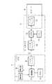
このICカード発行システムは、図1に示すように、パソコン(PC)1とこのPC1と通信ライン2を介して接続されているリーダライタ3とからなる。このリーダライタ3には、図示しないコネクタ等で接続される発行対象カードとしてのICカード4が装着されるようになっている。Hereinafter, an IC card issuing system as an IC card processing system (portable electronic medium processing system) of the present invention will be described with reference to the drawings.
As shown in FIG. 1, the IC card issuing system includes a personal computer (PC) 1 and a reader / writer 3 connected to the PC 1 via a communication line 2. The reader / writer 3 is mounted with an
PC1は、PC1の全体を制御する制御部5、制御用のプログラムが記憶されていたり種々のデータが記憶されるメモリ6、操作指示を行うキーボード等の操作部7、操作案内等が表示される表示部8、リーダライタ3とのデータのやり取りを行うインターフェース9により構成されている。 The PC 1 displays a
リーダライタ3は、リーダライタ3の全体を制御するCPU10、制御用のプログラムが記憶されていたり種々のデータが記憶されるメモリ11、PC1とのデータのやり取りを行うインターフェース12、ICカード4とのデータのやり取りを行うインターフェース13により構成されている。また、リーダライタ3には、ICカード4の挿入検知を行う検知器(図示しない)を有し、この検知結果をPC1へ出力するようになっている。また、リーダライタ3は、ICカード4の挿入検知時にICカード4の内容を読取り、アプリケーション等が未記録の発行用のカードか否かを示すデータをPC1へ出力するようにしても良い。 The reader / writer 3 includes a
ICカード4は、図2に示すように、ICカード4の全体を制御するCPU(制御素子)14、カード内部動作の制御用のプログラムが記憶されているマスクROM(プログラムメモリ)15、外部(リーダライタ3)と交換する電文の送受信バッファとCPU14の処理中のデータの一時格納バッファとして利用されるRAM(ワーキングメモリ)16、アプリケーション運用でその内容をリードライトして使用される運用データが格納され、認証用の鍵A等が格納されるEEPROM等で構成されるデータメモリ17、リーダライタ3とのデータのやり取りを行うインターフェース18、コンタクト部19により構成されている。
アプリケーションプログラムとしては、一例として、銀行取引業務処理、クレジット取引業務処理、プリペイド取引業務処理となっている。
上記CPU14、ROM15、RAM16、データメモリ17、インターフェース18は、ICチップ20により構成され、コンタクト部19およびICチップ20は一体的にモジュール化され、ICカード本体に埋設されている。As shown in FIG. 2, the
For example, the application program includes bank transaction business processing, credit transaction business processing, and prepaid transaction business processing.
The
CPU14には、図3に示すように、分岐番地レジスタ21a、…、分岐先番地レジスタ22a、…、プログラムカウンタ23、比較回路24a、…が内蔵されている。
分岐番地レジスタ21a、…は、電源供給等による起動時に、データメモリ17の領域17aに格納されている分岐する番地を記憶するものである。As shown in FIG. 3, the
The branch address register 21a,... Stores a branch address stored in the
分岐先番地レジスタ22a、…は、電源供給等による起動時に、データメモリ17の領域17aに格納されている分岐先のプログラムの番地情報を記憶するものである。
プログラムカウンタ23は、CPU14の動作中における次に実行するプログラムの番地を常に計数するものである。The branch destination address register 22a,... Stores the address information of the branch destination program stored in the
The
比較回路24a、…は、プログラムカウンタ23のカウント値と分岐番地レジスタ21a、…の値(分岐番地)とが一致するか否かをそれぞれ比較するものであり、一致した際、対応する分岐先番地レジスタ22a、…に記憶されている分岐先番地にジャンプするようになっている。 The
上記各管理情報をICカード4に対してコマンド電文で送り込むことがICカード4の発行処理となる。
すなわち、コマンド電文の処理用データとして上記管理情報を与え、コマンドコードと実行パラメータを設定してICカード4に対して送信することで、ICカード4は管理情報に従ってEEPROM17内にメモリ空間を確保し各ファイルを設定していく。Sending the above management information to the
That is, the management information is given as command message processing data, the command code and execution parameters are set and transmitted to the
すなわち、図1に示す構成において、ICチップ20の製造時に鍵Aを持たせ、このICチップ20を搭載したICカード4に対するコマンド電文を送信するPC1側にも、これらに対応した鍵Aを持たせる。
すなわち、鍵Aは、ICチップ20の製造時にハードウェアモジュールにて登録されており、発行に対する処理の終了時に消去されるようになっている。That is, in the configuration shown in FIG. 1, the key A is given when the
That is, the key A is registered in the hardware module when the
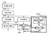
次に、上記のような構成において、ICカード4の発行処理について、図4、図5に示すフローチャートを参照しつつ説明する。
すなわち、ICカード4をICカード発行システムとしてのPC1に挿入することにより、ICカード4に電源電圧が供給される。これにより、ICカード4のCPU14はPC1からの命令電文を受信した際(ST1)、この命令を解析する(ST2)。Next, the issuing process of the
That is, the power supply voltage is supplied to the
この命令が鍵の照合、解錠(命令A)の際、CPU14は命令電文内の鍵Aとデータメモリ17の鍵Aとが一致するか否かの照合を行い、一致した際、鍵Aを解除し(鍵Aをデータメモリ17から削除し)する(ST3、4)。
また、上記命令が指定のデータの書込み(命令B)の際、CPU14は命令電文内の書込みアドレスと書込みデータをデータメモリ17に書込む(ST5、6)。When this command is a key collation / unlocking (command A), the
Further, when the command is writing of designated data (command B), the
上記した処理プログラムがデータメモリ17に搭載されている状態において、PC1から追加プログラムとしての命令BをICカード4のCPU14へ送信する。この命令Bには「番地1234」と追加プログラムおよび追加プログラムの格納番地(少なくとも1組の、分岐アドレス、プログラムおよびプログラムの格納場所を示す分岐先アドレス)が付加されている。 In a state where the above processing program is mounted on the data memory 17, the instruction B as an additional program is transmitted from the PC 1 to the
これにより、ICカード4のCPU14は命令Bとしての追加プログラム命令に基づいて、「番地1234」と追加プログラムおよび追加プログラムの格納番地をデータメモリ17の領域17aに格納する。この際、ICカード4のCPU14は物理的、回路的若しくはソフトウェア制御により1回のみ書き込みが可能であるように設定されている。たとえば、データメモリ17に書換え回数記憶部17bを設け、この書換え回数が所定回(1回)となってしまう際(ST20)、書き換えできないようになっている(ST21)。 Accordingly, the
上記ICカード4のCPU14は電源供給等による起動時、データメモリ17の領域17aに格納されている分岐する番地を分岐番地レジスタ21a、…に記憶し、分岐先のプログラムの番地情報を分岐先番地レジスタ22a、…に記憶する。
この後、ICカード4のCPU14は動作中において、次に実行するプログラムの番地を常にプログラムカウンタ23に持たせており、このカウント値が分岐番地レジスタ21a、…の値とが比較回路24a、…により比較される。これらの比較の結果、プログラムカウンタ23のカウント値が、分岐番地レジスタ21a、…のいずれかの分岐番地と一致した際(ST30)、ICカード4のCPU14は対応する分岐先番地レジスタ22a、…に記憶されている分岐先番地にジャンプして新しいプログラム(C)を実行する(ST31)。When the
Thereafter, during operation, the
たとえば、ICカード4のCPU14は命令Bの処理によりプログラムアドレスカウンタ23のカウント値が分岐アドレスとしての番地1234と一致した際(ST30)、データメモリ17の追加プログラムの格納番地に記憶されている追加プログラム「C」に基づく処理を実行する(ST31)。この追加プログラム「C」は、最後にマスクROM15の適切な番地にジャンプすることでマスクROM15のプログラムに処理を戻す。 For example, when the count value of the
上記したように、不揮発性メモリ(データメモリ)の一部に、分岐番地、プログラムおよびプログラムの格納場所を示す分岐先番地を一組または複数組書き込むことができ、CPUは実行するプログラムメモリの番地が前述の分岐番地と一致した場合は、分岐先番地に格納されているプログラムを実行するようにしたものである。 As described above, one or a plurality of branch destination addresses indicating a branch address, a program, and a program storage location can be written in a part of the nonvolatile memory (data memory), and the CPU stores the address of the program memory to be executed. Is the same as the above branch address, the program stored in the branch destination address is executed.
これにより、プログラムメモリであるマスクROMを作り直す(LSIを作り直す)ことなく、ICカードのプログラムを改変することが可能となり、新しいICカードを短期間に開発することが可能になる。
また、データメモリに書換え回数記憶部を設け、この書換え回数が1回となっている際、書き換えできないようにできる。
すなわち、分岐番地、分岐先番地およびプログラムは物理的、回路的若しくはソフトウェア制御により1回のみ書き込みが可能である。
分岐先番地は予め固定的に定められているものであっても良い。This makes it possible to modify the IC card program without recreating the mask ROM as the program memory (recreating the LSI) and to develop a new IC card in a short time.
In addition, a rewrite count storage unit can be provided in the data memory so that rewrite cannot be performed when the rewrite count is one.
That is, the branch address, the branch destination address, and the program can be written only once by physical, circuit, or software control.
The branch destination address may be fixed in advance.
すなわち、ICカードにおいて、CPUがマスクROM上のプログラムを実行中に、任意に設定できる特定の番地のプログラムを実行しようとした場合、任意に設定できる新しいプログラムへ制御を移す機能を有するものである。
また、プログラムを分岐する番地と、分岐後に実行される新しいプログラムはICカード用LSIに内蔵される不揮発性メモリに書き込まれ、上記の番地およびプログラムは複数設定できる。
上記の番地およびプログラムを不揮発性メモリへ書き込む場合、物理的、回路的あるいはソフトウェア的制御により1回のみ書き込みが可能であり、不正使用を防止することができる。In other words, the IC card has a function of transferring control to a new program that can be arbitrarily set when an attempt is made to execute a program at a specific address that can be arbitrarily set while the CPU is executing the program on the mask ROM. .
Further, an address at which the program is branched and a new program to be executed after the branch are written in a nonvolatile memory built in the IC card LSI, and a plurality of the addresses and programs can be set.
When the above address and program are written to the non-volatile memory, writing can be performed only once by physical, circuit or software control, and unauthorized use can be prevented.
すなわち、ベースとなる既存のICカードに対して比較的小規模のプログラム改変により新しいICカードが実現できる場合には、変更分のプログラムを後から書き加え、新しいICカードを実現しようとするものである。
これにより、短期間に新しいICカードを実現できる。In other words, when a new IC card can be realized by modifying a relatively small program with respect to an existing IC card as a base, the program for the change is added later to try to realize a new IC card. is there.
Thereby, a new IC card can be realized in a short time.
1…PC、 2…通信ライン、 3…リーダライタ 4…ICカード、 10…CPU、 11…メモリ、 14…CPU、 15…マスクROM、 16…RAM、 17…データメモリ、 18…インターフェース、 19…コンタクト部、 20…ICチップ、 21a…分岐番地レジスタ、 22a…分岐先番地レジスタ、 23…プログラムカウンタ、24a…比較回路。 DESCRIPTION OF SYMBOLS 1 ... PC, 2 ... Communication line, 3 ... Reader /
Claims (8)
Translated fromJapanese上記制御素子が少なくとも1つの特定アドレスを実行する際に、上記不揮発性メモリに記憶されている新たなプログラムを実行する実行手段を有することを特徴とする携帯可能電子媒体。In a portable electronic medium comprising an LSI having at least a mask ROM for storing a program, a nonvolatile memory, and a control element for control,
A portable electronic medium comprising execution means for executing a new program stored in the non-volatile memory when the control element executes at least one specific address.
上記不揮発性メモリに、分岐アドレス、プログラムおよびプログラムの格納場所を示す分岐先アドレスを一組または複数組記憶する記憶手段と、
上記制御素子により実行するマスクROMのアドレスが上記分岐アドレスと一致した際に、上記不揮発性メモリの分岐先アドレスに記憶されているプログラムを実行する実行手段と、
を有することを特徴とする携帯可能電子媒体。In a portable electronic medium comprising an LSI having at least a mask ROM for storing a program, a nonvolatile memory, and a control element for control,
Storage means for storing one or more sets of branch destination addresses indicating branch addresses, programs and program storage locations in the nonvolatile memory;
Execution means for executing a program stored in the branch destination address of the nonvolatile memory when the address of the mask ROM executed by the control element matches the branch address;
A portable electronic medium characterized by comprising:
上記不揮発性メモリにプログラムの改変用のデータを記憶する記憶手段と、
上記制御素子が上記マスクROMに格納されているプログラムに基づいて処理を行っている際に、このプログラムのアドレス値があらかじめ設定されている分岐値と一致するか否かを判断する判断手段と、
この判断手段により分岐値と一致すると判断した際に、上記記憶手段に記憶されているデータに基づくプログラムの改変を実行する実行手段と、
この実行手段によるプログラムの改変を実行後、上記マスクROMに格納されているプログラムに基づく処理へ移行する移行手段と、
を具備したことを特徴とする携帯可能電子媒体。In a portable electronic medium comprising an LSI having at least a mask ROM for storing a program, a nonvolatile memory, and a control element for control,
Storage means for storing program modification data in the nonvolatile memory;
When the control element performs processing based on a program stored in the mask ROM, determination means for determining whether the address value of the program matches a preset branch value;
An execution means for executing a modification of the program based on the data stored in the storage means when the determination means determines that the branch value matches the branch value;
After executing the program modification by the execution means, a transition means for shifting to processing based on the program stored in the mask ROM;
A portable electronic medium characterized by comprising:
上記端末が、
上記携帯可能電子媒体へ分岐アドレス、プログラムおよびプログラムの格納場所を示す分岐先アドレスの少なくとも一組を供給する供給手段を有し、
上記携帯可能電子媒体が、
上記外部機器から供給される分岐アドレス、プログラムおよびプログラムの格納場所を示す分岐先アドレスの少なくとも一組を記憶する記憶手段と、
上記制御素子により実行するマスクROMのアドレスが上記分岐アドレスと一致した際に、上記不揮発性メモリの分岐先アドレスに記憶されているプログラムを実行する実行手段とを有する、
ことを特徴とする携帯可能電子媒体取扱システム。In a portable electronic medium processing system comprising at least a mask ROM for storing a program, a nonvolatile memory, and an LSI incorporating a control element for control, and a terminal that handles the portable electronic medium,
The device
Supply means for supplying to the portable electronic medium at least one set of a branch address, a program, and a branch destination address indicating a storage location of the program;
The portable electronic medium is
Storage means for storing at least one set of a branch address supplied from the external device, a program, and a branch destination address indicating a storage location of the program;
Execution means for executing a program stored in the branch destination address of the nonvolatile memory when the address of the mask ROM executed by the control element coincides with the branch address;
A portable electronic medium handling system characterized by the above.
Priority Applications (1)
| Application Number | Priority Date | Filing Date | Title |
|---|---|---|---|
| JP2003287952AJP2005056259A (en) | 2003-08-06 | 2003-08-06 | Portable electronic medium and portable electronic medium handling device |
Applications Claiming Priority (1)
| Application Number | Priority Date | Filing Date | Title |
|---|---|---|---|
| JP2003287952AJP2005056259A (en) | 2003-08-06 | 2003-08-06 | Portable electronic medium and portable electronic medium handling device |
Publications (1)
| Publication Number | Publication Date |
|---|---|
| JP2005056259Atrue JP2005056259A (en) | 2005-03-03 |
Family
ID=34366784
Family Applications (1)
| Application Number | Title | Priority Date | Filing Date |
|---|---|---|---|
| JP2003287952APendingJP2005056259A (en) | 2003-08-06 | 2003-08-06 | Portable electronic medium and portable electronic medium handling device |
Country Status (1)
| Country | Link |
|---|---|
| JP (1) | JP2005056259A (en) |
Cited By (2)
| Publication number | Priority date | Publication date | Assignee | Title |
|---|---|---|---|---|
| WO2013042682A1 (en)* | 2011-09-21 | 2013-03-28 | 株式会社 東芝 | Ic card, portable electronic device, and ic card control method |
| KR101530479B1 (en)* | 2013-03-21 | 2015-06-19 | 가부시끼가이샤 도시바 | Ic card and portable electronic device |
- 2003
- 2003-08-06JPJP2003287952Apatent/JP2005056259A/enactivePending
Cited By (4)
| Publication number | Priority date | Publication date | Assignee | Title |
|---|---|---|---|---|
| WO2013042682A1 (en)* | 2011-09-21 | 2013-03-28 | 株式会社 東芝 | Ic card, portable electronic device, and ic card control method |
| JP2013069057A (en)* | 2011-09-21 | 2013-04-18 | Toshiba Corp | Ic card, portable electronic device and ic card control method |
| KR101553492B1 (en)* | 2011-09-21 | 2015-09-15 | 가부시끼가이샤 도시바 | Ic card, portable electronic device, and ic card control method |
| KR101530479B1 (en)* | 2013-03-21 | 2015-06-19 | 가부시끼가이샤 도시바 | Ic card and portable electronic device |
Similar Documents
| Publication | Publication Date | Title |
|---|---|---|
| US9418224B2 (en) | Portable electronic device and control method of portable electronic device | |
| KR20070037311A (en) | Portable Electronic Devices and IC Cards | |
| JP2004523827A (en) | Microprocessor circuit with auxiliary register bank | |
| JP2651426B2 (en) | IC card | |
| JP2005056259A (en) | Portable electronic medium and portable electronic medium handling device | |
| JP4836707B2 (en) | Portable electronic device and IC card | |
| JP2004348342A (en) | IC card and IC card processing method | |
| JP3251579B2 (en) | Portable electronic devices | |
| JP3302348B2 (en) | Portable electronic device and key matching method | |
| JP2004334745A (en) | IC card | |
| JPH01263892A (en) | portable electronic devices | |
| JP2609645B2 (en) | Portable electronic devices | |
| JP4784138B2 (en) | IC card and IC card program | |
| JP2003331236A (en) | Portable electronic devices | |
| JP2006172005A (en) | Portable electronic device | |
| JPH01194093A (en) | Portable electronic device | |
| JP2024139134A (en) | Electronic information storage medium, IC chip, method for writing issuance data, and program | |
| JP2025127976A (en) | IC card, computer program, IC chip, and reset response output method | |
| JP2006293706A (en) | Multi-application IC card with application update function | |
| JPH08171621A (en) | IC card | |
| JPS636690A (en) | portable electronic devices | |
| JP2022178821A (en) | Secure element, transaction control method and device | |
| JP2004334744A (en) | Issue system and method of portable electronic medium and portable electronic medium | |
| JP3054119B2 (en) | Portable electronic devices | |
| JP2675563B2 (en) | Portable electronic devices |
Legal Events
| Date | Code | Title | Description |
|---|---|---|---|
| A621 | Written request for application examination | Free format text:JAPANESE INTERMEDIATE CODE: A621 Effective date:20060725 | |
| A977 | Report on retrieval | Free format text:JAPANESE INTERMEDIATE CODE: A971007 Effective date:20090413 | |
| A131 | Notification of reasons for refusal | Free format text:JAPANESE INTERMEDIATE CODE: A131 Effective date:20090421 | |
| A02 | Decision of refusal | Free format text:JAPANESE INTERMEDIATE CODE: A02 Effective date:20090825 |