JP2005055880A - Liquid crystal display device and driving method thereof - Google Patents
Liquid crystal display device and driving method thereofDownload PDFInfo
- Publication number
- JP2005055880A JP2005055880AJP2004205103AJP2004205103AJP2005055880AJP 2005055880 AJP2005055880 AJP 2005055880AJP 2004205103 AJP2004205103 AJP 2004205103AJP 2004205103 AJP2004205103 AJP 2004205103AJP 2005055880 AJP2005055880 AJP 2005055880A
- Authority
- JP
- Japan
- Prior art keywords
- liquid crystal
- width
- electrode
- display device
- regulating means
- Prior art date
- Legal status (The legal status is an assumption and is not a legal conclusion. Google has not performed a legal analysis and makes no representation as to the accuracy of the status listed.)
- Pending
Links
Images


Classifications
- G—PHYSICS
- G02—OPTICS
- G02F—OPTICAL DEVICES OR ARRANGEMENTS FOR THE CONTROL OF LIGHT BY MODIFICATION OF THE OPTICAL PROPERTIES OF THE MEDIA OF THE ELEMENTS INVOLVED THEREIN; NON-LINEAR OPTICS; FREQUENCY-CHANGING OF LIGHT; OPTICAL LOGIC ELEMENTS; OPTICAL ANALOGUE/DIGITAL CONVERTERS
- G02F1/00—Devices or arrangements for the control of the intensity, colour, phase, polarisation or direction of light arriving from an independent light source, e.g. switching, gating or modulating; Non-linear optics
- G02F1/01—Devices or arrangements for the control of the intensity, colour, phase, polarisation or direction of light arriving from an independent light source, e.g. switching, gating or modulating; Non-linear optics for the control of the intensity, phase, polarisation or colour
- G02F1/13—Devices or arrangements for the control of the intensity, colour, phase, polarisation or direction of light arriving from an independent light source, e.g. switching, gating or modulating; Non-linear optics for the control of the intensity, phase, polarisation or colour based on liquid crystals, e.g. single liquid crystal display cells
- G02F1/133—Constructional arrangements; Operation of liquid crystal cells; Circuit arrangements
- G02F1/1333—Constructional arrangements; Manufacturing methods
- G02F1/1337—Surface-induced orientation of the liquid crystal molecules, e.g. by alignment layers
- G02F1/133707—Structures for producing distorted electric fields, e.g. bumps, protrusions, recesses, slits in pixel electrodes
- G—PHYSICS
- G02—OPTICS
- G02F—OPTICAL DEVICES OR ARRANGEMENTS FOR THE CONTROL OF LIGHT BY MODIFICATION OF THE OPTICAL PROPERTIES OF THE MEDIA OF THE ELEMENTS INVOLVED THEREIN; NON-LINEAR OPTICS; FREQUENCY-CHANGING OF LIGHT; OPTICAL LOGIC ELEMENTS; OPTICAL ANALOGUE/DIGITAL CONVERTERS
- G02F1/00—Devices or arrangements for the control of the intensity, colour, phase, polarisation or direction of light arriving from an independent light source, e.g. switching, gating or modulating; Non-linear optics
- G02F1/01—Devices or arrangements for the control of the intensity, colour, phase, polarisation or direction of light arriving from an independent light source, e.g. switching, gating or modulating; Non-linear optics for the control of the intensity, phase, polarisation or colour
- G02F1/13—Devices or arrangements for the control of the intensity, colour, phase, polarisation or direction of light arriving from an independent light source, e.g. switching, gating or modulating; Non-linear optics for the control of the intensity, phase, polarisation or colour based on liquid crystals, e.g. single liquid crystal display cells
- G02F1/133—Constructional arrangements; Operation of liquid crystal cells; Circuit arrangements
- G02F1/1333—Constructional arrangements; Manufacturing methods
- G02F1/1337—Surface-induced orientation of the liquid crystal molecules, e.g. by alignment layers
- G02F1/133753—Surface-induced orientation of the liquid crystal molecules, e.g. by alignment layers with different alignment orientations or pretilt angles on a same surface, e.g. for grey scale or improved viewing angle
- G—PHYSICS
- G02—OPTICS
- G02F—OPTICAL DEVICES OR ARRANGEMENTS FOR THE CONTROL OF LIGHT BY MODIFICATION OF THE OPTICAL PROPERTIES OF THE MEDIA OF THE ELEMENTS INVOLVED THEREIN; NON-LINEAR OPTICS; FREQUENCY-CHANGING OF LIGHT; OPTICAL LOGIC ELEMENTS; OPTICAL ANALOGUE/DIGITAL CONVERTERS
- G02F1/00—Devices or arrangements for the control of the intensity, colour, phase, polarisation or direction of light arriving from an independent light source, e.g. switching, gating or modulating; Non-linear optics
- G02F1/01—Devices or arrangements for the control of the intensity, colour, phase, polarisation or direction of light arriving from an independent light source, e.g. switching, gating or modulating; Non-linear optics for the control of the intensity, phase, polarisation or colour
- G02F1/13—Devices or arrangements for the control of the intensity, colour, phase, polarisation or direction of light arriving from an independent light source, e.g. switching, gating or modulating; Non-linear optics for the control of the intensity, phase, polarisation or colour based on liquid crystals, e.g. single liquid crystal display cells
- G02F1/137—Devices or arrangements for the control of the intensity, colour, phase, polarisation or direction of light arriving from an independent light source, e.g. switching, gating or modulating; Non-linear optics for the control of the intensity, phase, polarisation or colour based on liquid crystals, e.g. single liquid crystal display cells characterised by the electro-optical or magneto-optical effect, e.g. field-induced phase transition, orientation effect, guest-host interaction or dynamic scattering
- G02F1/139—Devices or arrangements for the control of the intensity, colour, phase, polarisation or direction of light arriving from an independent light source, e.g. switching, gating or modulating; Non-linear optics for the control of the intensity, phase, polarisation or colour based on liquid crystals, e.g. single liquid crystal display cells characterised by the electro-optical or magneto-optical effect, e.g. field-induced phase transition, orientation effect, guest-host interaction or dynamic scattering based on orientation effects in which the liquid crystal remains transparent
- G02F1/1393—Devices or arrangements for the control of the intensity, colour, phase, polarisation or direction of light arriving from an independent light source, e.g. switching, gating or modulating; Non-linear optics for the control of the intensity, phase, polarisation or colour based on liquid crystals, e.g. single liquid crystal display cells characterised by the electro-optical or magneto-optical effect, e.g. field-induced phase transition, orientation effect, guest-host interaction or dynamic scattering based on orientation effects in which the liquid crystal remains transparent the birefringence of the liquid crystal being electrically controlled, e.g. ECB-, DAP-, HAN-, PI-LC cells
- G—PHYSICS
- G02—OPTICS
- G02F—OPTICAL DEVICES OR ARRANGEMENTS FOR THE CONTROL OF LIGHT BY MODIFICATION OF THE OPTICAL PROPERTIES OF THE MEDIA OF THE ELEMENTS INVOLVED THEREIN; NON-LINEAR OPTICS; FREQUENCY-CHANGING OF LIGHT; OPTICAL LOGIC ELEMENTS; OPTICAL ANALOGUE/DIGITAL CONVERTERS
- G02F1/00—Devices or arrangements for the control of the intensity, colour, phase, polarisation or direction of light arriving from an independent light source, e.g. switching, gating or modulating; Non-linear optics
- G02F1/01—Devices or arrangements for the control of the intensity, colour, phase, polarisation or direction of light arriving from an independent light source, e.g. switching, gating or modulating; Non-linear optics for the control of the intensity, phase, polarisation or colour
- G02F1/13—Devices or arrangements for the control of the intensity, colour, phase, polarisation or direction of light arriving from an independent light source, e.g. switching, gating or modulating; Non-linear optics for the control of the intensity, phase, polarisation or colour based on liquid crystals, e.g. single liquid crystal display cells
- G02F1/133—Constructional arrangements; Operation of liquid crystal cells; Circuit arrangements
- G02F1/1333—Constructional arrangements; Manufacturing methods
- G02F1/1337—Surface-induced orientation of the liquid crystal molecules, e.g. by alignment layers
- G02F1/133776—Surface-induced orientation of the liquid crystal molecules, e.g. by alignment layers having structures locally influencing the alignment, e.g. unevenness
Landscapes
- Physics & Mathematics (AREA)
- Nonlinear Science (AREA)
- Chemical & Material Sciences (AREA)
- Crystallography & Structural Chemistry (AREA)
- General Physics & Mathematics (AREA)
- Optics & Photonics (AREA)
- Spectroscopy & Molecular Physics (AREA)
- Mathematical Physics (AREA)
- Liquid Crystal (AREA)
- Control Of Indicators Other Than Cathode Ray Tubes (AREA)
- Liquid Crystal Display Device Control (AREA)
Abstract
Translated fromJapaneseDescription
Translated fromJapanese本発明は、液晶表示装置およびその駆動方法に関し、特に動画を表示する用途に好適に用いられる液晶表示装置およびその駆動方法に関する。 The present invention relates to a liquid crystal display device and a driving method thereof, and more particularly, to a liquid crystal display device suitably used for displaying moving images and a driving method thereof.
近年、液晶表示装置(以下、「LCD」と言う。)が広く利用されるようになっている。これまでの主流は、誘電異方性が正のネマチック液晶をツイスト配向させたTN型LCDだった。このTN型LCDには、液晶分子の配向に起因する視角依存性が大きいという問題があった。 In recent years, liquid crystal display devices (hereinafter referred to as “LCD”) have been widely used. The mainstream so far has been TN type LCDs in which nematic liquid crystal with positive dielectric anisotropy is twisted. This TN type LCD has a problem that the viewing angle dependency due to the orientation of liquid crystal molecules is large.
そこで視角依存性を改善するために配向分割垂直配向型LCDが開発され、その利用が広まりつつある。例えば特許文献1には、配向分割垂直配向型液晶表示装置の1つであるMVA型液晶表示装置が開示されている。このMVA型液晶表示装置は、一対の電極間に設けられた垂直配向型液晶層を用いてノーマリーブラック(NB)モードで表示を行うLCDであり、ドメイン規制手段(例えばスリットまたは突起)を設け、それぞれの画素において電圧印加時に液晶分子が複数の異なる方向に倒れる(傾斜する)ように構成されている。 Therefore, in order to improve the viewing angle dependency, an alignment division vertical alignment type LCD has been developed and its use is spreading. For example,
最近では、液晶テレビだけでなく、PC用モニタや携帯端末機器(携帯電話やPDAなど)においても動画情報を表示するニーズが急速に高まっている。LCDで動画を高品位で表示するためには、液晶層の応答時間を短く(応答速度を速く)する必要があり、1垂直走査期間(典型的には1フレーム)内で所定の階調に到達することが要求される。 Recently, there is a rapidly increasing need for displaying moving image information not only on a liquid crystal television but also on a PC monitor and a mobile terminal device (such as a mobile phone and a PDA). In order to display a moving image with high quality on the LCD, it is necessary to shorten the response time of the liquid crystal layer (to increase the response speed), and to achieve a predetermined gradation within one vertical scanning period (typically one frame). It is required to reach.
MVA型LCDについては、例えば、特許文献1に黒−白間の応答時間を10msec以下にできることが開示されている。また、画素内に突起間の距離が異なる領域を設けることによって応答速度の異なる領域を設け、開口率を低下させることなく、見掛けの応答速度を改善できると記載されている(例えば特許文献1の図107〜図110参照)。 For an MVA type LCD, for example,
また、一方、LCDの応答特性を改善する駆動方法として、表示すべき階調に対応する電圧(所定の階調電圧)よりも高い電圧(「オーバーシュート電圧」という。)を印加する方法(「オーバーシュート駆動」という。)が知られている。オーバーシュート電圧(以下「OS電圧」という。)を印加することによって、中間調表示における応答特性を改善することができる。例えば、特許文献2には、オーバーシュート駆動(以下、「OS駆動」という。)されるMVA型LCDが開示されている。なお、特許文献2には、黒表示状態から高輝度中間調表示状態に切替わる際にはOS電圧を印加すべきでないと記載されている(例えば、特許文献2の図8参照)。これは、黒表示状態から高輝度中間調に切替わる際に、黒表示状態から低輝度中間調表示または白表示状態に切替わる際と同様にOS電圧(目標の透過率を与える電圧の1.25倍の電圧)を印加すると、透過率がオーバーシュートするためである、と記載されている。
しかしながら、本発明者の検討によると、上述したMVA型LCDなどの配向分割垂直配向型LCDにOS駆動を適用すると、新たな問題が発生することが分かった。この問題を図20(a)および(b)を参照しながら説明する。 However, according to the study of the present inventor, it has been found that when OS driving is applied to the alignment-divided vertical alignment type LCD such as the above-mentioned MVA type LCD, a new problem occurs. This problem will be described with reference to FIGS. 20 (a) and 20 (b).
図20(a)および(b)は、それぞれ、黒い(例えば0階調)背景90の中を中間調(例えば32/255階調)の四角形92を移動させた場合の表示の様子を模式的に示す図である。図20(a)は従来のMVA型LCDを通常の駆動方法で駆動した場合を示し、図20(b)は従来のMVA型LCDをOS駆動した場合を示している。なお、「32/255階調」とは、階調表示をγ2.2に設定した場合において、黒表示時(V0を印加時)の輝度を0、白表示時(V255を印加時)の輝度を1としたときに輝度が(32/255)2.2となる階調であり、そのときの階調電圧をV32と表記する。FIGS. 20A and 20B are schematic views of a display when a halftone (for example, 32/255 gradation)
OS駆動を行わない場合、配向分割垂直配向型LCDの応答速度が遅いために、図20(a)に模式的に示すように、四角形92の移動方向側のエッジ(端辺)92aが明瞭に観察されないことがある。一方、OS駆動方法を行うと、図20(b)に模式的に示すように、応答速度が改善され移動方向のエッジ92aは明瞭に観察されるものの、エッジ92aから少し遅れる部分に暗い帯92bが観察されるという現象が起こることがあった。 When OS driving is not performed, the response speed of the alignment-divided vertical alignment type LCD is slow. Therefore, as schematically shown in FIG. 20A, the
本発明者がこの原因を種々検討した結果、この現象は従来のTN型LCDにOS駆動方法を適用した場合には見られない新たな問題であり、配向分割垂直配向型LCDにおいて画素内に線状(帯状)に配置した配向規制手段(ドメイン規制手段)によって配向分割を行っていることに起因していることがわかった。 As a result of various investigations of the cause by the present inventors, this phenomenon is a new problem that cannot be seen when the OS driving method is applied to a conventional TN type LCD. It was found that this was caused by the alignment division being performed by the alignment regulating means (domain regulating means) arranged in a shape (band shape).
本発明は上記諸点に鑑みてなされたものであり、その主な目的は、高品位の動画表示が可能な配向分割垂直配向型LCDを提供することにある。 The present invention has been made in view of the above-mentioned points, and a main object thereof is to provide an alignment-divided vertical alignment type LCD capable of displaying a high-quality moving image.
本発明のある局面による液晶表示装置は、それぞれが、第1電極と、前記第1電極に対向する第2電極と、前記第1電極と前記第2電極の間に設けられた垂直配向型液晶層とを有する複数の画素を備え、前記液晶層の前記第1電極側に設けられ、第1の幅を有する第1配向規制手段と、前記液晶層の前記第2電極側に設けられ、第2の幅を有する第2配向規制手段と、前記第1配向規制手段と前記第2配向規制手段との間に規定され、第3の幅を有する液晶領域とを有し、前記第3の幅が2μm以上14μm以下であることを特徴とする。 A liquid crystal display device according to an aspect of the present invention includes a first electrode, a second electrode facing the first electrode, and a vertically aligned liquid crystal provided between the first electrode and the second electrode. A plurality of pixels having a layer, provided on the first electrode side of the liquid crystal layer, provided on the second electrode side of the liquid crystal layer, and provided on the second electrode side of the liquid crystal layer, A second alignment regulating means having a width of 2, a liquid crystal region having a third width defined between the first alignment regulating means and the second alignment regulating means, and the third width. Is 2 μm or more and 14 μm or less.
ある実施形態において、前記第1配向規制手段は前記第1の幅を有する帯状の形状を有し、前記第2配向規制手段は前記第2の幅を有する帯状の形状を有し、前記液晶領域は前記第3の幅を有する帯状の形状を有する。 In one embodiment, the first orientation regulating means has a strip shape having the first width, the second orientation regulating means has a strip shape having the second width, and the liquid crystal region. Has a strip-like shape having the third width.
ある実施形態において、前記第3の幅は12μm以下であることが好ましい。前記第3の幅は8μm以下であることがさらに好ましい。 In one embodiment, the third width is preferably 12 μm or less. More preferably, the third width is 8 μm or less.
本発明の他の局面による液晶表示装置は、それぞれが、第1電極と、前記第1電極に対向する第2電極と、前記第1電極と前記第2電極の間に設けられた垂直配向型液晶層とを有する複数の画素を備え、前記液晶層の前記第1電極側に設けられ、第1の幅を有する第1配向規制手段と、前記液晶層の前記第2電極側に設けられ、第2の幅を有する第2配向規制手段と、前記第1配向規制手段と前記第2配向規制手段との間に規定され、第3の幅を有する液晶領域とを有し、前記液晶領域は、前記第1配向規制手段に隣接し第1の応答速度を有する第1液晶領域と、前記第2配向規制手段に隣接し第2の応答速度を有する第2液晶領域と、前記第1液晶領域と前記第2液晶領域との間に規定され、前記第1および第2の応答速度よりも遅い第3の応答速度を有する第3液晶領域とを有し、前記第3液晶領域内において、黒表示状態から1垂直走査期間に32/255階調の透過率に到達する電圧を印加した後1垂直走査期間に相当する時間が経過したときの透過率が黒表示状態の透過率の2倍以下の領域の幅が2μm以下であることを特徴とする。 A liquid crystal display device according to another aspect of the present invention includes a first electrode, a second electrode facing the first electrode, and a vertical alignment type provided between the first electrode and the second electrode. A plurality of pixels having a liquid crystal layer, provided on the first electrode side of the liquid crystal layer, provided on the second electrode side of the liquid crystal layer, and first alignment regulating means having a first width; A second alignment regulating unit having a second width; a liquid crystal region having a third width defined between the first alignment regulating unit and the second alignment regulating unit; A first liquid crystal region having a first response speed adjacent to the first alignment control means, a second liquid crystal region having a second response speed adjacent to the second alignment control means, and the first liquid crystal region And the second liquid crystal region, and a third speed slower than the first and second response speeds. A third liquid crystal region having a response speed, and within the third liquid crystal region, one vertical scanning period after applying a voltage reaching a transmittance of 32/255 gradations in one vertical scanning period from the black display state The width of a region having a transmittance equal to or less than twice the transmittance in the black display state when a time corresponding to the time elapses is 2 μm or less.
ある実施形態において、前記第1配向規制手段は前記第1の幅を有する帯状の形状を有し、前記第2配向規制手段は前記第2の幅を有する帯状の形状を有し、前記液晶領域は前記第3の幅を有する帯状の形状を有する。 In one embodiment, the first orientation regulating means has a strip shape having the first width, the second orientation regulating means has a strip shape having the second width, and the liquid crystal region. Has a strip-like shape having the third width.
ある実施形態において、1垂直走査期間が16.7msecである。 In one embodiment, one vertical scan period is 16.7 msec.
ある実施形態において、前記第3の幅は2μm以上14μm以下である。前記第3の幅が12μm以下であることが好ましく、8μm以下であることがさらに好ましい。 In one embodiment, the third width is not less than 2 μm and not more than 14 μm. The third width is preferably 12 μm or less, and more preferably 8 μm or less.
ある実施形態において、前記第1配向規制手段がリブであり、前記第2配向規制手段は前記第2電極に設けられたスリットである。 In one embodiment, the first orientation regulating means is a rib, and the second orientation regulating means is a slit provided in the second electrode.
ある実施形態において、前記第1の幅が4μm以上20μm以下であり、前記第2の幅が4μm以上20μm以下である。 In one embodiment, the first width is 4 μm or more and 20 μm or less, and the second width is 4 μm or more and 20 μm or less.
ある実施形態において、前記第1電極が対向電極であり、前記第2電極が画素電極である。 In one embodiment, the first electrode is a counter electrode, and the second electrode is a pixel electrode.
ある実施形態において、前記液晶層の厚さが3μm未満である。 In one embodiment, the thickness of the liquid crystal layer is less than 3 μm.
ある実施形態において、前記第2の幅/前記液晶層の厚さは3以上である。 In one embodiment, the second width / the thickness of the liquid crystal layer is 3 or more.
ある実施形態において、前記第3の幅/前記第2の幅は1.5以下である。 In one embodiment, the third width / the second width is 1.5 or less.
ある実施形態において、前記液晶層を介して互いに対向するように配置された一対の偏光板を有し、前記一対の偏光板の透過軸は互いに略直交し、一方の透過軸は表示面の水平方向に配置され、前記第1配向規制手段および前記第2配向規制手段は、それぞれの延設方向が前記一方の透過軸と略45°を成すように配置されている。 In one embodiment, the liquid crystal layer has a pair of polarizing plates arranged to face each other, the transmission axes of the pair of polarizing plates are substantially orthogonal to each other, and one transmission axis is horizontal to the display surface The first orientation regulating means and the second orientation regulating means are arranged such that each extending direction forms approximately 45 ° with the one transmission axis.
ある実施形態において、中間調を表示する際に、所定の中間階調に対応する予め決められた階調電圧よりも高いオーバーシュート電圧を印加することができる駆動回路を更に備える。 In one embodiment, the apparatus further includes a drive circuit capable of applying an overshoot voltage higher than a predetermined gradation voltage corresponding to a predetermined intermediate gradation when displaying a halftone.
本発明の他の局面の液晶表示装置は、それぞれが、第1電極と、前記第1電極に対向する第2電極と、前記第1電極と前記第2電極の間に設けられた垂直配向型液晶層とを有する複数の画素を備え、前記液晶層の前記第1電極側に設けられ、第1の幅を有する帯状の第1配向規制手段と、前記液晶層の前記第2電極側に設けられ、第2の幅を有する帯状の第2配向規制手段と、前記第1配向規制手段と前記第2配向規制手段との間に規定され、第3の幅を有する帯状の液晶領域とを有し、前記第3の幅が2μm以上14μm以下であって、前記液晶層の厚さが3μm未満である。 The liquid crystal display device according to another aspect of the present invention includes a first electrode, a second electrode facing the first electrode, and a vertical alignment type provided between the first electrode and the second electrode. A plurality of pixels having a liquid crystal layer, provided on the first electrode side of the liquid crystal layer, provided on the second electrode side of the liquid crystal layer, and a strip-shaped first alignment regulating means having a first width; A band-shaped second alignment regulating means having a second width, and a band-shaped liquid crystal region having a third width defined between the first alignment regulating means and the second alignment regulating means. The third width is not less than 2 μm and not more than 14 μm, and the thickness of the liquid crystal layer is less than 3 μm.
本発明による液晶表示装置の駆動方法は、上記のいずれかの液晶表示装置の駆動方法であって、前の垂直走査期間の表示階調よりも高い中間階調を表示する際に、当該中間階調に対応する予め決められた階調電圧よりも高いオーバーシュート電圧を印加する工程を包含する。 The driving method of the liquid crystal display device according to the present invention is any one of the above-described driving methods of the liquid crystal display device, and when displaying an intermediate gray level higher than the display gray level of the previous vertical scanning period, Including a step of applying an overshoot voltage higher than a predetermined gradation voltage corresponding to the tone.
ある実施形態において、前記オーバーシュート電圧は、表示の輝度が1垂直走査期間に相当する時間内に当該中間階調に対応する所定の輝度に到達するように設定されている。 In one embodiment, the overshoot voltage is set so that the luminance of the display reaches a predetermined luminance corresponding to the intermediate gradation within a time corresponding to one vertical scanning period.
本発明による電子機器は、上記のいずれかの液晶表示装置を備えることを特徴とする。 An electronic apparatus according to the present invention includes any one of the liquid crystal display devices described above.
ある実施形態において、電子機器はテレビジョン放送を受信する回路をさらに備える。 In an embodiment, the electronic device further includes a circuit that receives a television broadcast.
本発明によると、OS駆動方法を適用した場合に高品位の動画表示が可能な配向分割垂直配向型LCDが提供される。本発明のLCDは、例えば、テレビジョン放送を受信する回路を備える液晶テレビとして好適に用いられる。また、パーソナルコンピュータやPDAなど動画を表示する用途に用いられる電子機器に好適に用いられる。 According to the present invention, there is provided an alignment division vertical alignment type LCD capable of displaying a high-quality moving image when the OS driving method is applied. The LCD of the present invention is suitably used as, for example, a liquid crystal television provided with a circuit for receiving television broadcasting. Moreover, it is used suitably for the electronic device used for the use which displays a moving image, such as a personal computer and PDA.
以下、図面を参照しながら本発明による実施形態のLCDおよびその駆動方法を説明する。 Hereinafter, an LCD according to an embodiment of the present invention and a driving method thereof will be described with reference to the drawings.
まず、本発明による実施形態の配向分割垂直配向型LCDの基本的な構成を図1(a)から(c)を参照しながら説明する。 First, a basic configuration of an alignment division vertical alignment type LCD according to an embodiment of the present invention will be described with reference to FIGS.
本発明による実施形態のLCDは、第1電極11と、第1電極11に対向する第2電極12と、第1電極11と第2電極12の間に設けられた垂直配向型液晶層13とを有する複数の画素を備える。垂直配向型液晶層13は、電圧無印加時に、誘電異方性が負の液晶分子を第1電極11および第2電極12の面に略垂直(例えば87°以上90°以下)に配向させたものである。典型的には、第1電極11および第2電極12のそれぞれの液晶層13側の表面に垂直配向膜(不図示)を設けることによって得られる。なお、配向規制手段としてリブ(突起)などを設けた場合、液晶分子はリブなどの液晶層側の表面に対して略垂直に配向することになる。 The LCD according to the embodiment of the present invention includes a
液晶層13の第1電極11側には第1配向規制手段(21、31、41)が設けられており、液晶層11の第2電極12側には第2配向規制手段(22、32、42)が設けられている。第1配向規制手段と第2配向規制手段との間に規定される液晶領域においては、液晶分子13aは、第1配向規制手段および第2配向規制手段からの配向規制力を受け、第1電極11と第2電極12との間に電圧が印加されると、図中に矢印で示した方向に倒れる(傾斜する)。すなわち、それぞれの液晶領域において液晶分子は一様な方向に倒れるので、それぞれの液晶領域はドメインとみなすことができる。本明細書における、配向規制手段は上記特許文献1および2に記載されているドメイン規制手段に対応する。 First alignment regulating means (21, 31, 41) is provided on the
第1配向規制手段および第2配向規制手段(これらを総称して「配向規制手段」と呼ぶことがある。)は各画素内で、それぞれ帯状に設けられており、図1(a)から(c)は帯状の配向規制手段の延設方向に直交する方向における断面図である。各配向規制手段のそれぞれの両側に液晶分子13aが倒れる方向が互いに180°異なる液晶領域(ドメイン)が形成される。 The first alignment regulating means and the second alignment regulating means (these may be collectively referred to as “orientation regulating means”) are provided in a strip shape within each pixel, and FIG. c) is a cross-sectional view in a direction orthogonal to the extending direction of the strip-shaped orientation regulating means. Liquid crystal regions (domains) in which the directions in which the
図1(a)に示すLCD10Aは、第1配向規制手段としてリブ21を有し、第2配向規制手段として第2電極12に設けられたスリット(開口部)22を有している。リブ21およびスリット22はそれぞれ帯状(短冊状)に延設されている。リブ21はその側面21aに略垂直に液晶分子13aを配向させることにより、液晶分子13aをリブ21の延設方向に直交する方向に配向させるように作用する。スリット22は、第1電極11と第2電極12との間に電位差が形成されたときに、スリット22の端辺近傍の液晶層13に斜め電界を生成し、スリット22の延設方向に直交する方向に液晶分子13aを配向させるように作用する。リブ21とスリット22とは、一定の間隔をあけて互いに平行に配置されており、互いに隣接するリブ21とスリット22との間に液晶領域(ドメイン)が形成される。 The
図1(b)に示すLCD10Bは、第1配向規制手段および第2配向規制手段としてそれぞれリブ31とリブ32とを有している点において、図1(a)のLCD10Aと異なる。リブ21とリブ32とは、一定の間隔をあけて互いに平行に配置されており、リブ31の側面31aおよびリブ32の側面32aに液晶分子13aを略垂直に配向させるように作用することによって、これらの間に液晶領域(ドメイン)が形成される。 The
図1(c)に示すLCD10Cは、第1配向規制手段および第2配向規制手段としてそれぞれスリット41とスリット42とを有している点において、図1(a)のLCD10Aと異なる。スリット41とスリット42とは、第1電極11と第2電極12との間に電位差が形成されたときに、スリット41および42の端辺近傍の液晶層13に斜め電界を生成し、スリット41および42の延設方向に直交する方向に液晶分子13aを配向させるように作用する。スリット41とスリット42とは、一定の間隔をあけて互いに平行に配置されており、これらの間に液晶領域(ドメイン)が形成される。 The
上述したように、第1配向規制手段と第2配向規制手段として、リブまたはスリットを任意の組み合わせで用いることができる。第1電極11と第2電極12は液晶層13を介して互いに対向する電極であればよく、典型的には一方が対向電極であり、他方が画素電極である。以下では、第1電極11が対向電極であり、第2電極12が画素電極である場合について、第1配向規制手段としてリブ11を有し、第2配向規制手段として画素電極に設けられたスリット22を有するLCD(図1(a)のLCD10Aに対応)を例に本発明の実施形態を説明する。図1(a)に示したLCD10Aの構成を採用すると、製造工程の増加を最小にできるという利点が得られる。画素電極にスリットを設けても付加的な工程は必要なく、一方、対向電極については、リブを設ける方がスリットを設けるよりも工程数の増加が少ない。もちろん、本発明は、配向規制手段としてリブだけを用いる構成、あるいはスリットだけを用いる構成にも適用できる。 As described above, ribs or slits can be used in any combination as the first orientation regulating means and the second orientation regulating means. The
本発明者は、種々検討した結果、図20(b)を参照しながら説明した上記の問題は、画素内に帯状に配置した第1配向規制手段および第2配向規制手段によって配向分割を行っていることに起因していることを見出し、第1配向規制手段と第2配向規制手段との間に規定される液晶領域の幅を14μm以下とすることによって、上記問題の発生を抑制できることを見出した。以下にこの問題の原因と本発明のLCDの効果を詳細に説明する。 As a result of various studies, the present inventor has solved the above problem described with reference to FIG. 20B by performing alignment division by the first alignment regulating means and the second alignment regulating means arranged in a strip shape in the pixel. And the occurrence of the above problem can be suppressed by setting the width of the liquid crystal region defined between the first alignment regulating means and the second alignment regulating means to 14 μm or less. It was. The cause of this problem and the effect of the LCD of the present invention will be described in detail below.
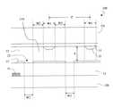
まず、図2および図3を参照しながら、本発明による実施形態のLCDの基本構成を説明する。図2は本発明によるLCD100の断面構造を模式的に示す部分断面図であり、図3はLCD100の画素部100aの平面図である。LCD100は図1(a)のLCD10Aと同様の基本構成を有するので、共通する構成要素は共通の参照符号で示す。 First, the basic configuration of the LCD according to the embodiment of the present invention will be described with reference to FIGS. FIG. 2 is a partial cross-sectional view schematically showing a cross-sectional structure of the
LCD100は、第1基板(例えばガラス基板)10aと第2基板(例えばガラス基板)10bとの間に垂直配向型液晶層13を有している。第1基板10aの液晶層13側の表面には対向電極11が形成されており、その上にさらにリブ21が形成されている。リブ21上を含む対向電極11の液晶層13側表面のほぼ全面に垂直配向膜(不図示)が設けられている。リブ21は図3に示すように、帯状に延設されており、隣接するリブ21は互いに平行に配設されており、その間隔(ピッチ)Pは一定であり、リブ21の幅(延設方向に直交する方向の幅)W1も一定である。 The
第2基板(例えばガラス基板)10bの液晶層13側の表面には、ゲートバスライン(走査線)およびソースバスライン(信号線)51とTFT(不図示)が設けられており、これらを覆う層間絶縁膜52が形成されている。この層間絶縁膜52上に画素電極12が形成されている。ここでは、厚さが1.5μm以上3.5μm以下の透明樹脂膜を用いて平坦な表面を有する層間絶縁膜52を設けており、このことによって、画素電極12をゲートバスラインおよび/またはソースバスラインと部分的に重ねて配置することが可能となり、開口率を向上できるという利点が得られる。 On the surface of the second substrate (for example, glass substrate) 10b on the
画素電極12には帯状のスリット22が形成されており、スリット22を含む画素電極12上のほぼ全面に垂直配向膜(不図示)が形成されている。スリット22は、図3に示すように、帯状に延設されており、隣接するスリット22は互いに平行に配設されており、且つ、隣接するリブ21の間隔を略二等分するように配置されている。スリット22の幅(延設方向に直交する方向の幅)W2は一定である。上述のスリットやリブの形状およびこれらの配置は、製造プロセスのばらつきや、基板を貼り合わせる際の位置合わせ誤差などの影響で、設計値からずれることがあり、上記の説明はこれらを排除するものではない。 A strip-shaped
互いに平行に延設された帯状のリブ21とスリット22との間に幅W3を有する帯状の液晶領域13Aが規定される。それぞれの液晶領域13Aは、その両側のリブ21およびスリット22によって配向方向が規制されており、リブ21およびスリット22のそれぞれの両側に液晶分子13aが倒れる方向が互いに180°異なる液晶領域(ドメイン)が形成されている。LCD100は、図3に示すように、リブ21およびスリット22は互いに90°異なる2つの方向に沿って延設されており、画素部100Aは液晶分子13aの配向方向が90°異なる4種類の液晶領域13Aを有している。リブ21およびスリット22の配置はこの例に限られないが、このように配置することによって、良好な視野角特性を得ることができる。 A strip-shaped
また、第1基板10aおよび第2基板10bの両側に配置される一対の偏光板(不図示)は、透過軸が互いに略直交(クロスニコル状態)するように配置される。90°ずつ配向方向が異なる4種類の液晶領域13Aの全てに対して、それぞれの配向方向と偏光板の透過軸とが45°を成すように配置すれば、液晶領域13Aによるリタデーションの変化を最も効率的に利用することができる。すなわち、偏光板の透過軸がリブ21およびスリット22の延設方向と略45°を成すように配置することが好ましい。また、テレビのように、観察方向を表示面に対して水平に移動することが多い表示装置においては、一対の偏光板の一方の透過軸を表示面に対して水平方向に配置することが、表示品位の視野角依存性を抑制するために好ましい。 A pair of polarizing plates (not shown) arranged on both sides of the
上述の構成を有するMVA型LCD100は、視野角特性に優れた表示を行うことができるが、OS駆動を行うと図20(b)に示した現象が発生することがある。図4および図5を参照しながら、この現象を詳細に説明する。 The
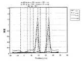
図4は、OS駆動したときのLCD100の画素における輝度分布の変化を、高速カメラを用いて測定した結果を示す図である。なお、わかりやすさのために5℃で測定した結果を示す。横軸はリブ21およびスリット22の延設方向に直交する方向であり、隣接するスリット22の内の一方の幅方向の中央を原点とした位置を示している。輝度分布は、0msec(V0印加状態:この時点でOSV32を印加)、OSV32を印加した後16msec後、18msec後、500msec後の測定結果を示している。なお、OSV32を印加した垂直走査期間(ここでは1フレーム=16.7msec)の次の垂直走査期間後以降は、OSV32を印加後500msec経過するまでV32を印加し続けた。また、縦軸は、遮光領域の輝度を0とし、後述する第3液晶領域R3の500msec後の到達輝度を0.1として、相対輝度で示している。 FIG. 4 is a diagram illustrating a result of measuring a change in luminance distribution in the pixels of the
ここで用いたLCD100の具体的なセルパラメータは、液晶層の厚さd=3.9μm、リブピッチP=53μm、リブ21の幅W1は16μm(側面部の幅4μm×2を含む。)、スリット22の幅W2は10μm、液晶領域13Aの幅W3は13.5μmであり、黒電圧(V0)=1.2V、白電圧(V255)=7.1V、γ値を2.2としたときの32階調(透過率1.04%)の電圧(V32)=2.44V、OS電圧(OSV32)=2.67Vである。OS電圧(OSV32)は、黒状態(V0を印加した状態)から16msec後に画素全体の輝度(透過率)が32階調の輝度になるよう設定した。 The specific cell parameters of the
図4から分かるように、液晶領域13Aの内、リブ21の側面21a付近の領域(「第1液晶領域R1」という。)の輝度が高く、且つ、18msecで最高輝度に到達した後、輝度は低下する。これに対し、第1液晶領域R1以外の領域では、時間の経過ともに輝度が単調に上昇し、一旦高くなった輝度が低下することは無い。なお、図4に示した液晶領域13Aの内、スリット22付近の領域(「第2液晶領域R2」という。)は、スリット22の近傍に発生する斜め電界の影響を受けるので、液晶領域13Aの中央付近の領域(リブ21とスリット22との中央付近の領域、「第3液晶領域R3」という。)よりも応答速度が速い。このように帯状のリブ21とスリット22との間に規定される帯状の液晶領域13Aには、3つの異なる応答速度で特徴付けられる3つの液晶領域(R1、R2およびR3)が形成されている。 As can be seen from FIG. 4, the luminance of the region near the
なお、ここで例示したLCD100では第1配向規制手段(リブ21)と第2配向規制手段(スリット22)とが応答速度に対して与える影響の程度が互いに異なっているので、応答速度が互いに異なる3つの液晶領域が形成されたが、第1配向規制手段と第2配向規制手段の影響が同じ場合には、応答速度が同程度に速い2つの液晶領域(R1およびR2)とこれらよりも応答速度が遅い1つの液晶領域(R3)とが形成される。 Note that in the
次に、図5(a)および(b)を参照しながら、画素部分100Aの全体の透過率の時間変化を説明する。縦軸は0階調の透過率を0%、32階調の透過率を100%としている。また、図5(a)は測定温度が25℃、図5(b)は測定温度が5℃の結果をそれぞれ示している。 Next, with reference to FIGS. 5 (a) and 5 (b), the temporal change in the overall transmittance of the pixel portion 100A will be described. The vertical axis represents 0% transmittance at 0 gradation and 100% transmittance at 32 gradations. FIG. 5A shows the results when the measurement temperature is 25 ° C., and FIG. 5B shows the results when the measurement temperature is 5 ° C.
図5(a)中の曲線5A−1および曲線5A−2は、液晶層の厚さdが3.9μmの場合で、曲線5A−1がOS駆動なし、曲線5A−2がOS駆動ありの結果を示している。一方、曲線5A−3および曲線5A−4はセルギャップが2.8μmの場合であり、曲線5A−3がOS駆動なし、曲線5A−4はOS駆動ありの結果を示している。図5(b)は同様に、曲線5B−1および曲線5B−2は液晶層の厚さdが3.9μmの場合で、曲線5B−1がOS駆動なし、曲線5B−2がOS駆動ありの結果を示している。曲線5B−3および曲線5B−4はセルギャップが2.8μmの場合であり、曲線5B−3がOS駆動なし、曲線5B−4はOS駆動ありの結果を示している。なお、いずれの液晶層についても、液晶材料は、回転粘度γ1が約140mPa・s、フロー粘度νが約20mm2/sであり、且つ、それぞれの液晶層のリタデーション(厚さd×複屈折率Δn)が約300nmとなるように液晶材料を選んだ。
図5(a)および(b)から明らかなように、25℃および5℃のいずれの温度においてもOS駆動を行うと、OS電圧を印加した垂直走査期間内で所定の透過率(100%)に到達した後、一旦透過率が低下し、再び透過率が徐々に上昇し、再び所定の透過率に到達するという現象が見られる。このように、透過率の時間変化に極小値が現れる現象を「角(つの)応答」と呼ぶことがある。 As is apparent from FIGS. 5A and 5B, when OS driving is performed at both temperatures of 25 ° C. and 5 ° C., a predetermined transmittance (100%) is obtained within the vertical scanning period in which the OS voltage is applied. After reaching the value, the transmittance once decreases, the transmittance gradually increases again, and the phenomenon that the predetermined transmittance is reached again is observed. In this way, the phenomenon in which the minimum value appears in the temporal change in transmittance may be referred to as “corner response”.
また、図5(a)と図5(b)との比較から、液晶分子の応答速度が遅い5℃の方がこの現象が顕著であり、透過率の時間変化における極小値の値が小さく、且つ、所定の透過率に到達するのに要する時間が長い。さらに、図5(a)および図5(b)において、液晶層の厚さdの違いを比較すると、いずれの温度においても、液晶層の厚さが大きい方が応答速度が遅く、透過率が低下している時間が長いことが分かる。これらの傾向は、図20(b)に示した現象の目視による観察結果と対応した。 Further, from the comparison between FIG. 5A and FIG. 5B, this phenomenon is more remarkable at 5 ° C. where the response speed of the liquid crystal molecules is slower, and the minimum value in the temporal change in transmittance is small. In addition, it takes a long time to reach the predetermined transmittance. Further, in FIGS. 5A and 5B, when the difference in the thickness d of the liquid crystal layer is compared, the response speed is slower and the transmittance is higher when the thickness of the liquid crystal layer is larger at any temperature. It can be seen that the time of decline is long. These tendencies corresponded to the visual observation results of the phenomenon shown in FIG.
このように、透過率の時間変化に極小値が現れるために図20(b)に示した暗い帯92bが観察されることが分かった。また、透過率の時間変化に極小値が現れる原因は、図4を参照しながら説明した第1液晶領域R1、第2液晶領域R2および第3液晶領域R3の間で応答速度の違いが大きいためであることも分かった。再び図4を参照しながら、この現象を説明する。 Thus, it has been found that the
リブ21の近傍に位置する第1液晶領域R1の液晶分子は、リブ21の側面21aの影響を受けて、電圧が印加される前から傾斜しており、それゆえに応答速度が速い。画素全体の透過率が1フレーム期間内に0階調から32階調となるように設定したOS電圧(OSV32)を印加すると、第1液晶領域R1の液晶分子の応答速度が速いので、第1液晶領域R1の透過率は、少なくともV32が定常的に印加されたときの透過率(図4中のt=500secの曲線で示される透過率)を超え、場合によってはOS電圧(OSV32)に対応する透過率またはそれに近い透過率にまで到達する。これに対し、第1液晶領域R1以外の領域(第2液晶領域R2および第3液晶領域R3)の応答速度は遅く、OSV32を印加しても1フレーム期間内にV32に対応する透過率に到達できない。 The liquid crystal molecules in the first liquid crystal region R1 located in the vicinity of the
V32を印加する次のフレーム期間以降(t>16.7msec)では、第1液晶領域R1の透過率は、V32に対応する透過率まで単調に減少する。これに対し、第2液晶領域R2および第3液晶領域R3の透過率はV32に対応する透過率まで単調に増大する。 After the next frame period in which V32 is applied (t> 16.7 msec), the transmittance of the first liquid crystal region R1 monotonously decreases to the transmittance corresponding to V32. On the other hand, the transmittance of the second liquid crystal region R2 and the third liquid crystal region R3 monotonously increases to the transmittance corresponding to V32.
OSV32を印加したフレーム期間内に画素全体の透過率がV32に対応する透過率に到達しても、そのときの透過率には応答速度が速過ぎる成分(V32に対応する透過率を超えた透過率成分)を含んでいるため、OSV32の印加を止めて所定の階調電圧V32を印加すると、応答速度が速過ぎる成分が応答速度の遅い成分(第2液晶領域および第3液晶領域R3の透過率成分)が増大する速度よりも速い速度で所定の透過率まで減少するので、画素全体の透過率は一時的に減少する。その後、応答速度の遅い成分の増大とともに画素全体の透過率が増大する。これが図5(a)および(b)に示した画素部分の透過率の時間変化の詳細である。 Even if the transmittance of the entire pixel reaches the transmittance corresponding to V32 within the frame period in which the
OS駆動方法はTN型LCDにも適応されているが、TN型LCDでは上述の角応答は見られない。TN型LCDにおける配向分割は、異なる方向にラビング処理された配向膜によって各液晶領域(ドメイン)における液晶分子の配向方向を規制することによって達成されており、分割された領域全体に配向膜から面状に(2次元的に)配向規制力を与えている。従って、それぞれの液晶領域には応答速度の分布が発生しない。これに対し、配向分割垂直配向型LCDにおいては、線状(1次元的)に設けられた配向規制手段によって配向分割を行っているために、配向規制手段の配向規制力の違いだけで無く、配向規制手段からの距離によって応答速度の異なる領域が形成される。 Although the OS driving method is also applied to the TN type LCD, the above-mentioned angular response is not seen in the TN type LCD. The alignment division in the TN type LCD is achieved by regulating the alignment direction of the liquid crystal molecules in each liquid crystal region (domain) by the alignment film rubbed in different directions. The orientation regulating force is given to the shape (two-dimensionally). Accordingly, no response speed distribution occurs in each liquid crystal region. On the other hand, in the alignment division vertical alignment type LCD, since the alignment division is performed by the alignment regulating means provided linearly (one-dimensionally), not only the difference in the alignment regulating force of the alignment regulating means, Regions with different response speeds are formed depending on the distance from the orientation regulating means.
次に、この角応答特性、すなわちOS電圧印加後に透過率が極小値をとる現象の発生を抑制するために、セルパラメータ(液晶層厚さd、リブピッチP、リブ幅W1、スリット幅W2、液晶領域幅W3およびリブ高さなど)を変えて、図2および図3に示した基本構成を有するMVA型LCDを作製し、その応答特性を評価した。 Next, cell parameters (liquid crystal layer thickness d, rib pitch P, rib width W1, slit width W2, liquid crystal) are controlled in order to suppress the occurrence of this angular response characteristic, that is, the phenomenon that the transmittance takes a minimum value after the OS voltage is applied. The MVA type LCD having the basic configuration shown in FIGS. 2 and 3 was manufactured by changing the region width W3 and the rib height, and the response characteristics were evaluated.
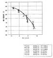
その結果、液晶層厚さdを小さくすることによって、図5(a)および(b)を参照しながら上述したように、応答速度が速くなることが確認された。また、リブ幅W1およびスリット幅W2を大きくすることによって応答速度が若干速くなる傾向が認められた。リブを高くすることによっても応答速度が若干速くなった。しかしながら、リブ幅W1、スリット幅W2およびリブ高さを調整することによって得られる応答速度の改善効果はいずれも小さかった。これらに対し、液晶領域幅W3を狭くすると応答特性を大きく改善できることが分かった。結果の一部を図6に示す。 As a result, it was confirmed that by reducing the liquid crystal layer thickness d, the response speed was increased as described above with reference to FIGS. 5 (a) and 5 (b). Further, it was recognized that the response speed tends to be slightly increased by increasing the rib width W1 and the slit width W2. The response speed also increased slightly by increasing the ribs. However, the effect of improving the response speed obtained by adjusting the rib width W1, the slit width W2, and the rib height was small. On the other hand, it was found that the response characteristics can be greatly improved by narrowing the liquid crystal region width W3. A part of the results is shown in FIG.
図6は、液晶層厚さd、リブ高さが異なる6種類のセル構成について、液晶領域幅W3を変えたLCDについて、図5に示した透過率の時間変化を測定した結果得られた、OS電圧印加後の透過率の極小値を示している。それぞれ32階調の透過率を100%としている。また、透過率の極小値(「極小透過率」ということもある。)は、液晶層厚さdに関わらずほぼ一定の値であった。ここで用いたLCDにおけるリブ幅W1およびスリット幅W2はいずれも約5μm以上約20μm以下の範囲内にあり、リブピッチPは約25μm以上約58μm以下の範囲内にある。図6に示した結果は、パネル表面温度が25℃における測定結果である。 FIG. 6 is a result of measuring the change in transmittance over time shown in FIG. 5 for an LCD in which the liquid crystal region width W3 is changed for six types of cell configurations having different liquid crystal layer thickness d and rib height. The minimum value of the transmittance after applying the OS voltage is shown. The transmittance of 32 gradations is 100%. Further, the minimum value of transmittance (sometimes referred to as “minimum transmittance”) was a substantially constant value regardless of the liquid crystal layer thickness d. The rib width W1 and the slit width W2 in the LCD used here are both in the range of about 5 μm to about 20 μm, and the rib pitch P is in the range of about 25 μm to about 58 μm. The result shown in FIG. 6 is a measurement result when the panel surface temperature is 25 ° C.
まず、図6から分かることは、6種類(リブ幅W1およびスリット幅W2の違いを含めるとさらに多種類となる)のセル構成に関らず、液晶領域幅W3と極小透過率との間に強い相関関係があることである。次に、液晶領域幅W3を小さくすることによって、極小透過率がほぼ単調に増加する、すなわち応答特性が改善されることが分かる。 First, it can be seen from FIG. 6 that there is no difference between the liquid crystal region width W3 and the minimum transmittance regardless of the cell configuration of six types (which includes more types including the difference between the rib width W1 and the slit width W2). There is a strong correlation. Next, it can be seen that by reducing the liquid crystal region width W3, the minimum transmittance increases almost monotonously, that is, the response characteristic is improved.
図6の結果から、液晶領域幅W3を約14μm以下にすることによって、極小透過率は85%以上となり、約12μm以下にすることによって極小透過率を90%以上にできることが分かる。極小透過率が85%以上であると図20(b)に示した暗い帯92bはかなり観察され難くなる。もちろん、極小透過率が90%以上であると暗い帯92bはさらに観察され難くなる。 From the results of FIG. 6, it can be seen that the minimum transmittance is 85% or more by setting the liquid crystal region width W3 to about 14 μm or less, and the minimum transmittance can be 90% or more by setting it to about 12 μm or less. When the minimum transmittance is 85% or more, the
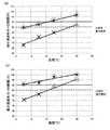
実際に13型VGAのLCDを試作し、この応答特性の改善効果を25人で主観評価した結果を図7(a)および(b)に示す。ここで用いた13型VGAタイプのLCD(本発明および従来のLCD)は、後に説明する図14に示した結果が得られたLCDと同じであり、OS駆動条件も後述する条件と同じである。ここでは、極小透過率を85%以上または90%以上に設定することによって得られる効果を説明する。 FIGS. 7A and 7B show the results of subjective evaluation of the response characteristics improvement effect by 25 people who actually made a prototype of a 13-inch VGA LCD. The 13-inch VGA type LCD (the present invention and the conventional LCD) used here is the same as the LCD from which the result shown in FIG. 14 described later is obtained, and the OS drive conditions are the same as those described later. . Here, the effect obtained by setting the minimum transmittance to 85% or more or 90% or more will be described.
図7(a)および(b)に示したグラフの横軸は、LCDの表示面の温度(「動作温度」とする。)であり、縦軸はOS駆動を行ったときの極小透過率である。LCDの動作温度が変わると、液晶材料の粘度などの物性が変化する結果、LCDの応答特性が変化することになる。動作温度が低いほど応答特性は低下し、高いほど応答特性は改善される。ここでは、動作温度を5℃、15℃、25℃および40℃とした。また、表示階調の変化が小さいほど、OS駆動による角応答が発生しやすくなる。表示階調を0階調から32階調に切替えた場合(32階調の背景中を0階調の四角を移動させた場合)の結果を図7(a)に示し、0階調から64階調に切替えた場合(64階調の背景中を0階調の四角を移動させた場合)の結果を図7(b)に示す。図7(a)および(b)中の各点に重ねて示した記号(○、△、×)が主観評価の結果を示している。この場合にも角応答の影響によって図20(b)に示し暗い帯92bと同様に暗い帯が観察される。○は暗い帯がほとんど全ての人にほとんど視認されないことを示し、△は一部の観察者には暗い帯が視認されるもののほとんど気にならない程度であることを示し、×はほとんど全ての人に暗い帯が視認されることを示している。 The horizontal axis of the graphs shown in FIGS. 7A and 7B is the temperature of the display surface of the LCD (referred to as “operating temperature”), and the vertical axis is the minimum transmittance when OS driving is performed. is there. When the operating temperature of the LCD changes, the response characteristics of the LCD change as a result of changes in physical properties such as the viscosity of the liquid crystal material. The response characteristic is lowered as the operating temperature is lower, and the response characteristic is improved as the operating temperature is higher. Here, the operating temperatures were 5 ° C, 15 ° C, 25 ° C and 40 ° C. In addition, the smaller the change in display gradation, the more likely an angular response due to OS driving occurs. FIG. 7A shows the result when the display gradation is switched from 0 gradation to 32 gradation (when the square of 0 gradation is moved in the background of 32 gradations). FIG. 7B shows the result when the gradation is switched (when the square of 0 gradation is moved in the background of 64 gradations). Symbols (◯, Δ, ×) superimposed on each point in FIGS. 7A and 7B indicate the result of subjective evaluation. In this case as well, a dark band is observed due to the influence of the angular response, similar to the
図7(a)および(b)からわかるように、極小透過率が85%以上であると主観評価の結果は△又は○となり、極小透過率が90%以上であると主観評価の結果は○となる。従来のLCDの場合は、0階調から32階調に切替えると(図7(a))、動作温度が40℃のときだけ極小透過率が85%以上となり、一般的な使用温度(室温)である25℃では極小透過率は80%程度に過ぎず、主観評価は×となっている。これに対し、本発明によるLCDは、0階調から32階調に切替えた場合(図7(a))、動作温度が5℃であっても極小透過率は85%以上あり、25℃以上の動作温度では90%以上の極小透過率が得られる。さらに、0階調から64階調に切替えた場合(図7(b))、動作温度が5℃でも90%以上の極小透過率が得られる。 As can be seen from FIGS. 7A and 7B, when the minimum transmittance is 85% or more, the result of subjective evaluation is Δ or ○, and when the minimum transmittance is 90% or more, the result of subjective evaluation is ○ It becomes. In the case of a conventional LCD, when switching from 0 gradation to 32 gradation (FIG. 7A), the minimum transmittance becomes 85% or more only when the operating temperature is 40 ° C., and the general use temperature (room temperature) At 25 ° C., the minimum transmittance is only about 80%, and the subjective evaluation is x. In contrast, when the LCD according to the present invention is switched from 0 gradation to 32 gradation (FIG. 7A), the minimum transmittance is 85% or more even at an operating temperature of 5 ° C., and 25 ° C. or more. A minimum transmittance of 90% or more can be obtained at the operating temperature. Further, when the gradation is switched from 0 gradation to 64 gradation (FIG. 7B), a minimum transmittance of 90% or more can be obtained even at an operating temperature of 5 ° C.
このように、液晶領域幅W3を約14μm以下にすることによって極小透過率を85%以上とし、あるいは、液晶領域幅W3を約12μm以下にすることによって極小透過率を90%以上とすると、OS駆動を行っても暗い帯が視認され難い、あるいはほとんど視認されない、動画表示特性が優れたMVA型LCDが得られる。 Thus, if the minimum transmittance is 85% or more by setting the liquid crystal region width W3 to about 14 μm or less, or the minimum transmittance is 90% or more by setting the liquid crystal region width W3 to about 12 μm or less, the OS It is possible to obtain an MVA type LCD having excellent moving image display characteristics in which a dark band is hardly visible or hardly visible even when driven.
現在市販されている12機種(3社、パネルサイズ:15インチから37インチ)のMVA型LCD(図1(c)に示したPVA型LCDを含む。)の液晶領域幅W3は約15μm以上約27μm以下の範囲(第1配向規制手段の幅W1は約7μm以上約15μm以下、第2配向規制手段の幅W2は約7μm以上約10μm以下)にあり、上記の結果(例えば図6)に基づくと、本実施形態と同様のOS駆動を行うと暗い帯が観察されることになる。 The liquid crystal area width W3 of 12 types (3 companies, panel size: 15 to 37 inches) of MVA type LCDs (including the PVA type LCD shown in FIG. 1C) currently on the market is about 15 μm or more. It is in the range of 27 μm or less (the width W1 of the first orientation regulating means is about 7 μm or more and about 15 μm or less, and the width W2 of the second orientation regulating means is about 7 μm or more and about 10 μm or less), and based on the above results (for example, FIG. 6) Then, when OS driving similar to that of the present embodiment is performed, a dark band is observed.
次に、液晶領域幅W3を小さくすることによって応答特性が改善される理由を図8および図4を参照しながら説明する。 Next, the reason why the response characteristic is improved by reducing the liquid crystal region width W3 will be described with reference to FIGS.
図8は液晶領域幅W3と第3液晶領域R3の幅との関係を示すグラフである。第3液晶領域R3は、図4を参照しながら上述したように、液晶領域13Aの内リブ21およびスリット22から離れた位置にあり、応答速度が最も遅い領域である。 FIG. 8 is a graph showing the relationship between the liquid crystal region width W3 and the width of the third liquid crystal region R3. As described above with reference to FIG. 4, the third liquid crystal region R3 is located at a position away from the
ここで、第3液晶領域R3の幅を定量的にあらわすために、次のように定義する。0階調を表示している状態(黒表示状態)から32階調に到達させるOS電圧(OSV32)を印加して1フレーム後の透過率が、黒表示状態の透過率の2倍以下の領域を第3液晶領域R3とする。液晶領域幅W3が異なるLCDについて、図4と同様の透過率分布の時間変化を測定し、上記の定義に従って求めた第3液晶領域R3の幅を求めた結果をプロットしグラフを図8に示している。図8には25℃および5℃での測定結果を示している。 Here, in order to quantitatively represent the width of the third liquid crystal region R3, the following definition is made. An area in which the transmittance after one frame after applying the OS voltage (OSV32) for reaching 32 gradations from the state displaying the 0 gradation (black display state) is less than twice the transmittance in the black display state Is a third liquid crystal region R3. For LCDs having different liquid crystal region widths W3, the time variation of the transmittance distribution similar to that in FIG. 4 is measured, and the results of obtaining the width of the third liquid crystal region R3 obtained according to the above definition are plotted. ing. FIG. 8 shows the measurement results at 25 ° C. and 5 ° C.
図8に示すグラフはいずれも傾きが1の直線であり、このことは第1液晶領域R1および第2液晶領域R2の幅が液晶領域幅W3に依存せずに一定であることを示している。従って、R3幅=液晶領域幅W3−第1液晶領域R1の幅−第2液晶領域R2の幅の関係が成立している。液晶領域13Aの応答特性が改善されると第3液晶領域R3が実質的に存在しないようになるが、図8のグラフ(直線)から、負の値を有する第3液晶領域R3の幅を求めることができる。この第3液晶領域R3の幅は、液晶領域13Aの応答特性を表すパラメータとすることができる。 The graphs shown in FIG. 8 are all straight lines having an inclination of 1, which indicates that the widths of the first liquid crystal region R1 and the second liquid crystal region R2 are constant without depending on the liquid crystal region width W3. . Therefore, the relationship of R3 width = liquid crystal region width W3−width of first liquid crystal region R1−width of second liquid crystal region R2 is established. When the response characteristic of the
図8から分かるように、25℃においては、液晶領域幅W3が約12μm以下となると第3液晶領域R3幅が零になる。即ち、上記定義で表される応答速度が遅い第3液晶領域R3が実質的に無くなる。これは図6において極小透過率が90%以上に液晶領域幅W3に対応しており、良い相関が認められる。 As can be seen from FIG. 8, at 25 ° C., when the liquid crystal region width W3 is about 12 μm or less, the third liquid crystal region R3 width becomes zero. That is, the third liquid crystal region R3 having a slow response speed represented by the above definition is substantially eliminated. This corresponds to the liquid crystal region width W3 having a minimum transmittance of 90% or more in FIG. 6, and a good correlation is recognized.
一方、図8に示した5℃の結果を見ると、液晶領域幅W3が約8μm以下となると第3液晶領域R3幅が零になる。従って、より優れた応答特性(動画表示特性)を得るためには液晶領域幅W3が約8μm以下であることが好ましいことが分かる。 On the other hand, looking at the result of 5 ° C. shown in FIG. 8, when the liquid crystal region width W3 is about 8 μm or less, the third liquid crystal region R3 width becomes zero. Therefore, it can be seen that the liquid crystal region width W3 is preferably about 8 μm or less in order to obtain better response characteristics (moving picture display characteristics).
図6に示したグラフを第3液晶領域R3の幅に対してプロットしなおしたものを図9に示す。図9から明らかなように、第3液晶領域R3幅を約2μm以下にすることによって極小透過率を85%以上にすることができ、約0μm以下にすることによって極小透過率を90%以上にすることができる。 FIG. 9 shows a re-plot of the graph shown in FIG. 6 with respect to the width of the third liquid crystal region R3. As is clear from FIG. 9, the minimum transmittance can be increased to 85% or more by setting the width of the third liquid crystal region R3 to about 2 μm or less, and the minimum transmittance can be set to 90% or more by setting it to about 0 μm or less. can do.
上述したように、液晶領域幅W3を狭くすることによって応答特性を改善し、OS駆動を行った場合に発生する角応答(図5参照)における極小透過率を所定の透過率の85%以上にすることができる。従って、角応答に起因する不具合は殆ど観察されず、良好な動画表示が可能なLCDが提供される。 As described above, the response characteristic is improved by narrowing the liquid crystal region width W3, and the minimum transmittance in the angular response (see FIG. 5) generated when the OS is driven is set to 85% or more of the predetermined transmittance. can do. Accordingly, an LCD capable of displaying a good moving image is provided with almost no defects caused by the angular response.
なお、液晶領域幅W3が2μmを下回るとLCDの製造が困難となるので、液晶領域幅W3は2μm以上であることが好ましく、同様の理由から、リブ幅W1およびスリット幅W2は4μm以上であることが好ましい。 Note that if the liquid crystal region width W3 is less than 2 μm, it becomes difficult to manufacture an LCD. Therefore, the liquid crystal region width W3 is preferably 2 μm or more. For the same reason, the rib width W1 and the slit width W2 are 4 μm or more. It is preferable.
本発明のLCDに適用されるOS駆動方法は特に限定されず、公知のOS駆動方法を適宜採用することができる。また、例えば、上述したように32階調ごと(例えばV0からV32)に表示階調を切り替える際に1垂直走査期間で所定の透過率となるようにOS電圧を設定し、32階調未満の変化のときに印加するOS電圧の大きさは、32階調の変化に対応して決めたOS電圧の大きさを補間して求めることができる。さらに、変化の前後の階調に応じてOS電圧の大きさを変えても良いし、上記特許文献2に記載されているように、一部の階調間の変化にはOS電圧を印加しないようにしてもよい。 The OS driving method applied to the LCD of the present invention is not particularly limited, and a known OS driving method can be appropriately employed. Further, for example, as described above, when the display gradation is switched every 32 gradations (for example, from V0 to V32), the OS voltage is set so that a predetermined transmittance is obtained in one vertical scanning period, and less than 32 gradations. The magnitude of the OS voltage applied at the time of change can be obtained by interpolating the magnitude of the OS voltage determined corresponding to the change in 32 gradations. Furthermore, the magnitude of the OS voltage may be changed according to the gradation before and after the change, and as described in
ここでは、32階調ごとに1フレーム期間後に所定の透過率となるOS電圧の大きさを求め、これを補間することによって各階調変化に対応するOS電圧の大きさを決めた。このようにして決めたOS電圧を用いて、液晶領域幅W3を14μm以下に設定した本実施形態のMVA型LCDを駆動したところ、良好な動画表示を実現することができた。 Here, the magnitude of the OS voltage that gives a predetermined transmittance after one frame period is obtained every 32 gradations, and the magnitude of the OS voltage corresponding to each gradation change is determined by interpolation. When the MVA type LCD of the present embodiment in which the liquid crystal region width W3 was set to 14 μm or less was driven using the OS voltage determined in this way, good moving image display could be realized.
次に、本実施形態のMVA型LCDの開口率および透過率について説明する。図2および図3から分かるように、MVA型LCDにおいて、液晶領域幅W3を小さくするということは、開口率:{(画素面積−リブ面積−スリット面積)/画素面積}を低下させることになるので、表示輝度が低下することになる。従って、応答特性を改善するために配向規制手段の間隔(すなわち、ここでいう液晶領域の幅W3)を一様に狭くすると開口率が低下するので、例えば、特許文献1(例えば図107参照)には、画素内の一部の領域では隣接する配向規制手段間の間隔を狭くし、画素内の他の領域では配向規制手段間の間隔を広くすることによって、開口率を低下させること無く、応答特性を改善できると記載されている。しかしながら、上述した理由から、特許文献1に記載されているように、配向規制手段間の間隔が狭い領域と広い領域とを作ると、応答速度が大きく異なる領域が形成されるので(特に、応答速度が遅い領域の面積が大きくなるので、)角応答の問題が顕著となる。 Next, the aperture ratio and transmittance of the MVA type LCD according to this embodiment will be described. As can be seen from FIGS. 2 and 3, in the MVA type LCD, reducing the liquid crystal region width W3 decreases the aperture ratio: {(pixel area−rib area−slit area) / pixel area}. As a result, the display brightness is lowered. Therefore, if the interval between the alignment regulating means (that is, the width W3 of the liquid crystal region here) is uniformly narrowed in order to improve the response characteristics, the aperture ratio decreases. For example, Patent Document 1 (see, for example, FIG. 107). In some areas in the pixel, the interval between the adjacent alignment regulating means is narrowed, and in other areas in the pixel, the interval between the orientation regulating means is widened, without reducing the aperture ratio. It is described that the response characteristics can be improved. However, for the reasons described above, as described in
これに対し、図2および図3に示した本発明による実施形態のLCDの基本構成では、第1配向規制手段21と第2配向規制手段22との間隔(帯状の液晶領域13Aの幅W3)が上記の範囲に設定されているので、角応答の問題の発生を抑制することができる。また、上述の例では、液晶領域13Aの幅が画素内で一定の場合について説明したが、製造プロセス上の要因(例えば基板の貼り合せ工程における位置合わせ誤差)によって、幅W3が異なる液晶領域13Aが1つの画素内に形成されても、それぞれの液晶領域13Aの幅W3が上記条件を満足すれば、角応答の問題の発生を抑制することができる。 On the other hand, in the basic configuration of the LCD according to the embodiment shown in FIGS. 2 and 3, the distance between the first alignment regulating means 21 and the second alignment regulating means 22 (width W3 of the strip-like
さらに、今回の一連の検討で明らかになったのであるが、本実施形態のMVA型LCDは、液晶領域幅W3を従来よりも狭くしたにも関わらず、表示輝度が低下しなかった。これは、液晶領域幅W3を従来よりも狭くすることによって、画素の単位面積当たりの透過率(以下、「透過効率」という。)が向上するという予想外の効果によるものである。透過効率は、画素の透過率を実測し、この値を開口率で除することによって求められる。ここでは透過効率を0〜1までの数値で表す。 Further, as has been clarified by a series of examinations this time, the display luminance of the MVA type LCD of the present embodiment did not decrease even though the liquid crystal region width W3 was made narrower than before. This is due to an unexpected effect that the transmittance per unit area of the pixel (hereinafter referred to as “transmission efficiency”) is improved by making the liquid crystal region width W3 narrower than before. The transmission efficiency is obtained by actually measuring the transmittance of the pixel and dividing this value by the aperture ratio. Here, the transmission efficiency is represented by a numerical value from 0 to 1.
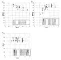
図6に関連して説明した種々のセルパラメータを有する本実施形態のLCDについて求めた透過効率の結果を図10(a)および(b)に示す。図10(a)は横軸に(液晶領域幅W3/スリット幅W2)をとったグラフであり、図10(b)は横軸に(スリット幅W2/液晶層厚さd)をとったグラフである。また、図10(c)にそれぞれのLCDの開口率を示す。 FIGS. 10A and 10B show the results of transmission efficiency obtained for the LCD of this embodiment having various cell parameters described in relation to FIG. FIG. 10A is a graph with (liquid crystal region width W3 / slit width W2) on the horizontal axis, and FIG. 10B is a graph with (slit width W2 / liquid crystal layer thickness d) on the horizontal axis. It is. FIG. 10C shows the aperture ratio of each LCD.
図10(a)から分かるように、(液晶領域幅W3/スリット幅W2)を1.5以下とすることによって、従来(約0.7)よりもむしろ透過効率が向上する。また、図10(b)から分かるように、(スリット幅W2/液晶層厚さd)が約3以上のときに透過効率は約0.7以上の高い値に安定する。 As can be seen from FIG. 10A, by setting (liquid crystal region width W3 / slit width W2) to 1.5 or less, the transmission efficiency is improved rather than the conventional (about 0.7). Further, as can be seen from FIG. 10B, when (slit width W2 / liquid crystal layer thickness d) is about 3 or more, the transmission efficiency is stabilized at a high value of about 0.7 or more.
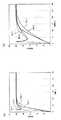
液晶領域幅W3を狭くすると、図10(a)に示したように透過効率が向上する理由を図11を参照しながら説明する。図11は、スリット22の近傍の液晶領域13Aにおける液晶分子13aの配向の様子を模式的に示している。液晶領域13A内の液晶分子13aのうち、帯状に延びる液晶領域13Aの端辺(長辺)13Xの近傍の液晶分子13aは、斜め電界の影響を受けて、長辺13Xに垂直な面内で傾く。これに対し、液晶領域13Aの長辺13Xと交差する端辺(短辺)13Yの近傍で斜め電界の影響を受ける液晶分子13aは、長辺13Xの近傍の液晶分子13aとは異なる方向に傾く。すなわち、液晶領域13Aの短辺13Yの近傍の液晶分子13aは、スリット22による配向規制力によって規定される所定の配向方向と異なる方向に傾き、液晶領域13Aの液晶分子13aの配向を乱すように作用することになる。液晶領域13Aの幅W3が狭くなる(すなわち短辺の長さ/長辺の長さが小さくなる)と、液晶領域13A中の液晶分子13aの内、スリット22の配向規制力の影響を受けて所定の方向に傾く液晶分子13aの割合が増加することになり、透過効率が上昇する。従って、液晶領域幅W3を狭くすることによって、液晶領域13A内の液晶分子13aの配向を安定化する効果が得られ、その結果、透過効率が向上する。 The reason why the transmission efficiency is improved when the liquid crystal region width W3 is narrowed as shown in FIG. 10A will be described with reference to FIG. FIG. 11 schematically shows the orientation of the
種々検討した結果、液晶領域幅W3を狭くすることによる配向安定化効果(透過効率向上効果)は、液晶層厚さdが小さい、例えば3μm未満のときに顕著となることがわかった。液晶層厚さdが小さくなると、スリット22による斜め電界の作用が強くなる反面、画素電極12の周辺に設けられるゲートバスラインやソースバスラインからの電界の影響や、あるいは隣接する画素電極からの電界の影響を受けるようになる。これらの電界は液晶領域13A内の液晶分子13aの配向を乱すように作用する。従って、液晶領域13A内の液晶分子13aの配向が乱れやすい、液晶層厚さdが小さい場合に、上記配向安定化の効果が顕著になると考えられる。 As a result of various studies, it has been found that the alignment stabilization effect (transmission efficiency improvement effect) by narrowing the liquid crystal region width W3 becomes significant when the liquid crystal layer thickness d is small, for example, less than 3 μm. When the liquid crystal layer thickness d decreases, the action of the oblique electric field by the
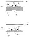
なお、本実施形態で例示したLCDは、図2に示したように、ゲートバスラインやソースバスライン51上を覆う比較的厚い層間絶縁膜52上に画素電極12が形成されている。図12(a)および(b)を参照しながら、層間絶縁膜52による液晶分子13aの配向に対する影響を説明する。 In the LCD exemplified in this embodiment, the
図12(a)に示すように、本実施形態のLCDが有する層間絶縁膜52は比較的厚く(例えば厚さ約1.5μm以上約3.5μm以下)形成されている。従って、画素電極12とゲートバスラインやソースバスライン51とが層間絶縁膜52を介して部分的に重なってもこれらの間に形成される容量は小さく、表示品位に影響しない。また、隣接する画素電極12間に存在する液晶分子13aの配向に影響する電界は、図中に電気力線で模式的に示したように、対向電極11と画素電極12との間に生成される斜め電界がほとんどであり、ソースバスライン51の影響はほとんど受けない。 As shown in FIG. 12A, the
これに対し、図12(b)に模式的に示すように、比較的薄い層間絶縁膜(例えば、厚さ数百nmのSiO2膜)52’が形成されている場合、例えばソースバスライン51と画素電極12が層間絶縁膜52’を介して部分的に重なると比較的大きな容量が形成され、表示品位が低下するので、これを防止するために、画素電極12とソースバスライン51とが重ならないように設ける。この場合、隣接する画素電極12間に存在する液晶分子13aは、図中に電気力線で示したように、画素電極12とソースバスライン51との間に生成される電界の影響を大きく受け、画素電極12の端部の液晶分子13aの配向が乱れることになる。On the other hand, when a relatively thin interlayer insulating film (for example, a SiO2 film having a thickness of several hundreds nm) 52 ′ is formed as schematically shown in FIG. 12B, for example, the
図12(a)および(b)の比較から明らかなように、例示した実施形態のLCDのように比較的厚い層間絶縁膜52を設けると、液晶分子13aがゲートバスラインやソースバスラインによる電界の影響を受けず、配向規制手段によって液晶分子13aを所望の方向に良好に配向させることができるとい利点が得られる。また、このように比較的厚い層間絶縁膜52を設けることによって、バスラインからの電界の影響が小さくなるので、液晶層の厚さを小さくすることによる配向安定化効果が顕著に発揮される。 As is clear from the comparison between FIGS. 12A and 12B, when the relatively thick
上記の実施形態では、第1および第2配向規制手段の組み合わせとして、リブ21とスリット22との組み合わせを例示したが、リブとリブとの組み合わせ、およびスリットとスリットとの組み合わせにおいても同様の効果を得ることができる。またスリット22の配向規制力を強める目的で、スリット22の下部(液晶層13と反対側)に当該電極と異なる電位の電極(例えば、画素電極にスリットが形成されている場合は補助容量電極)を配置してもよい。 In the above embodiment, the combination of the
応答特性の観点からは、液晶層13の厚さdは小さい方が好ましく(例えば図5参照)、上記構成を備えるLCDの液晶層13の厚さdを3μm未満とするとことによって、さらに高品位な動画表示が可能なMVA型LCDが得られる。 From the viewpoint of response characteristics, it is preferable that the thickness d of the
図13(a)および(b)を参照しながら、液晶層13の厚さdを小さくすることによって応答特性が改善されることを説明する。 With reference to FIGS. 13A and 13B, it will be described that the response characteristic is improved by reducing the thickness d of the
図13(a)に示すグラフの横軸は、液晶領域13Aの幅W3と液晶層13の厚さdとの積であり、縦軸は透過率の戻り時間である。ここで「透過率の戻り時間」の定義を図13(b)を参照しながら説明する。上述したように、OS駆動を行うと透過率は図13(b)に模式的に示すように時間変化する。すなわち、OS電圧を印加(0ms時点)することによって1フレーム後(16.7msec時点)に透過率が所定の値に到達した後、透過率は低下し極小値を取る。この後、透過率は所定の階調電圧に対応する透過率に徐々に近づく。この透過率変化において、最初に所定の透過率に到達した時点(16.7ms)から、極小値を経て所定の透過率の99%まで透過率が到達する時点までの時間を「戻り時間」という。ここでは、表示階調を0階調から32階調に切替えた場合の結果を示している。 The horizontal axis of the graph shown in FIG. 13A is the product of the width W3 of the
図13(a)からわかるように、d×W3が小さいほど透過率戻り時間が短くなっており、応答特性が優れている。液晶領域幅W3は上述したように14μm以下に設定することが好ましく、液晶層の厚さdを3μm未満とすると透過率の戻り時間が約100ms以下になることがわかる。 As can be seen from FIG. 13 (a), the smaller the d × W3, the shorter the transmittance return time, and the better the response characteristics. As described above, the liquid crystal region width W3 is preferably set to 14 μm or less, and when the thickness d of the liquid crystal layer is less than 3 μm, the transmittance return time is about 100 ms or less.
このように、液晶領域の幅W3を14μm以下とし、更に液晶層の厚さdを3μm未満とすることによって、角応答に起因する不具合の発生を抑制することが出来るとともに、さらに応答特性を改善することができる。 Thus, by setting the width W3 of the liquid crystal region to 14 μm or less and the thickness d of the liquid crystal layer to less than 3 μm, it is possible to suppress the occurrence of defects caused by angular response and further improve the response characteristics. can do.
実際に13型VGAのLCDを試作し、動画表示性能を評価した結果を説明する。セルパラメータは、液晶層厚さdを2.5μm、液晶領域幅W3を10.7μmとした以外は、図4に示したLCD100について例示した値とほぼ同じ値である。また、比較のために液晶層厚さdが3.4μm、液晶領域幅W3が15.4μmの従来品の特性を合せて評価した。 A description will be given of the result of actually producing a 13-inch VGA LCD and evaluating the moving image display performance. The cell parameters are almost the same as the values exemplified for the
本発明による実施形態のLCDと従来のLCDについて、画素部分の全体の透過率の時間変化(角応答特性)を評価した結果を図14(a)〜(c)に示す。図14(a)は0階調から32階調へ、図14(b)は0階調から64階調へ、図14(c)は0階調から96階調に表示を切替えた場合の角応答特性を示している。本発明のLCDおよび従来のLCDのいずれもオーバーシュート駆動を行った場合の結果を示している。ここでは、動作温度が5℃の場合についての結果を示している。 14A to 14C show the results of evaluating the temporal change (angular response characteristics) of the overall transmittance of the pixel portion for the LCD according to the embodiment of the present invention and the conventional LCD. 14A shows the case where the display is switched from 0 gradation to 32 gradations, FIG. 14B shows the case where the display is changed from 0 gradations to 64 gradations, and FIG. 14C shows the case where the display is changed from 0 gradations to 96 gradations. The angular response characteristic is shown. Both the LCD of the present invention and the conventional LCD show the results when overshoot driving is performed. Here, the result for the case where the operating temperature is 5 ° C. is shown.
図14(a)〜(c)から明らかなように、本発明による実施形態のLCDは応答特性が改善されているため、極小透過率の値がいずれも従来のLCDよりも高く、所定の階調に対応する透過率の80%以上となっている。また、上述したように主観評価を行った結果、従来のLCDをOS駆動すると暗い帯が観察されたのに対し、本発明による実施形態のLCDをOS駆動しても暗い帯はほとんど確認できなかった。 As is apparent from FIGS. 14A to 14C, the LCD of the embodiment according to the present invention has improved response characteristics. Therefore, all of the values of the minimum transmittance are higher than those of the conventional LCD, and the predetermined level. The transmittance corresponding to the tone is 80% or more. Further, as a result of the subjective evaluation as described above, a dark band was observed when the conventional LCD was driven by the OS, whereas a dark band was hardly confirmed even when the LCD of the embodiment according to the present invention was driven by the OS. It was.
以下、表1から表6を参照しながら、本発明のLCDと従来のLCDとについて、OS駆動の具体的な条件と、応答特性を説明する。表1から表6は、5℃における結果を示している。 Hereinafter, specific conditions for OS driving and response characteristics of the LCD of the present invention and the conventional LCD will be described with reference to Tables 1 to 6. Tables 1 to 6 show the results at 5 ° C.
表1から表6において、左端(start)に記載されている数値は、初期状態における表示階調を示し、上段(end)に記載されている数値は、書き換え後の表示階調を示している。ここでは、初期状態の表示階調が0階調の場合を例示する。 In Tables 1 to 6, the numerical value described at the left end (start) indicates the display gradation in the initial state, and the numerical value described in the upper stage (end) indicates the display gradation after rewriting. . Here, the case where the display gradation in the initial state is 0 gradation is illustrated.
OS電圧値(ここでは、対応する表示階調で示す。)は、本発明のLCDについては表1に示したように設定し、従来のLCDについては表4に示したように設定した。例えば、表1に示したように、0階調から32階調に表示を切替える際には、OS電圧として94階調に対応する電圧値を有する電圧を印加した。また、表1および4に示していない階調については、表1および4のように設定した関係に基づいて図15に示すグラフを作成し、補完することによって対応するOS階調を求めた。 The OS voltage value (indicated here by the corresponding display gradation) was set as shown in Table 1 for the LCD of the present invention, and as shown in Table 4 for the conventional LCD. For example, as shown in Table 1, when switching the display from 0 gradation to 32 gradations, a voltage having a voltage value corresponding to 94 gradations was applied as the OS voltage. For gradations not shown in Tables 1 and 4, the graph shown in FIG. 15 was created based on the relationships set as shown in Tables 1 and 4, and the corresponding OS gradation was obtained by complementation.
また、本発明のLCDの応答時間を表2および表3に示す。表2はOS駆動無しの場合、表3はOS駆動有りの場合の結果を示している。同様に、従来のLCDの応答時間を表5および表6に示す。表5はOS駆動無しの場合、表6はOS駆動有りの場合の結果を示している。なお、応答時間は、それぞれの階調変化における所定の透過率の変化を0%〜100%として、透過率が10%から90%まで変化するに要した時間(単位msec)を表している。 Tables 2 and 3 show the response time of the LCD of the present invention. Table 2 shows the results when the OS is not driven, and Table 3 shows the results when the OS is driven. Similarly, Tables 5 and 6 show response times of conventional LCDs. Table 5 shows the results when the OS is not driven, and Table 6 shows the results when the OS is driven. The response time represents the time (unit: msec) required for the transmittance to change from 10% to 90%, assuming that the change in the predetermined transmittance in each gradation change is 0% to 100%.
OS電圧値は、表1および表4に示したように、32階調ごとに、それぞれの階調に1フレーム期間内に所定の階調に到達するようにOS電圧を設定した。例えば、本発明のLCDについては、表1に示したように0階調から32階調に切り替える場合のOS電圧(OSV32)をV94(94階調に対応する電圧)とした。すなわち、OS駆動では、通常の駆動ではV32を印加するところV94を印加した。一方、従来のLCDについては、表4に示したように0階調から32階調に切り替える場合のOS電圧(OSV32)をV156(156階調に対応する電圧)とした。従来のLCDの方がOS電圧値が高いのは、表2と表5とを比較したら明らかなように、本発明のLCDの方が応答特性に優れている(応答時間が短い)ためである。このことからも、上述した構成によって応答特性が改善されていることがわかる。 As shown in Tables 1 and 4, the OS voltage value was set such that every 32 gradations, each gradation reached a predetermined gradation within one frame period. For example, in the LCD of the present invention, as shown in Table 1, the OS voltage (OSV32) when switching from 0 gradation to 32 gradations was set to V94 (voltage corresponding to 94 gradations). That is, in OS driving, V94 is applied when V32 is applied in normal driving. On the other hand, for the conventional LCD, as shown in Table 4, the OS voltage (OSV32) when switching from the 0th gradation to the 32nd gradation was set to V156 (voltage corresponding to the 156 gradation). The reason why the OS voltage value of the conventional LCD is higher is that the LCD of the present invention has better response characteristics (response time is shorter), as is clear when Table 2 and Table 5 are compared. . This also shows that the response characteristics are improved by the above-described configuration.
表2に示した応答時間からわかるように、本発明のLCDはOS駆動を行わないと、低階調を表示する際の応答時間が1フレーム期間(16.7msec)を超える場合がある。これに対し、OS駆動を行うと、表3に示したように、全ての階調において応答時間を1フレーム期間よりも短くすることができる。これに加えて、上述したように角応答の問題も発生しない。従来のLCDをOS駆動すると、表6に示したように応答時間は大幅に改善されるものの、未だ1フレーム期間を超える場合があり、さらに、上述したように角応答の問題も発生する。 As can be seen from the response time shown in Table 2, the LCD of the present invention may exceed one frame period (16.7 msec) when the OS is not driven to display a low gradation. On the other hand, when OS driving is performed, as shown in Table 3, the response time can be made shorter than one frame period in all gradations. In addition to this, the problem of angular response does not occur as described above. When the conventional LCD is driven by the OS, the response time is greatly improved as shown in Table 6, but it may still exceed one frame period, and the problem of angular response also occurs as described above.

本発明による実施形態の液晶表示装置は、上述したようにOS駆動することによって、優れた動画表示特性を発揮する。従って、例えば、テレビジョン放送を受信する回路をさらに設けることによって、高品位の動画表示が可能な液晶テレビとして好適に用いることができる。なお、OS駆動を実現するためには、公知の方法を広く適用するこが可能であり、所定の中間階調に対応する予め決められた階調電圧よりも高いOS電圧(階調電圧を用いることも出来る)を印加することができる駆動回路を更に設けても良いし、あるいはソフト的にOS駆動を実行することもできる。 The liquid crystal display device according to the embodiment of the present invention exhibits excellent moving image display characteristics by OS driving as described above. Therefore, for example, by further providing a circuit for receiving television broadcasting, it can be suitably used as a liquid crystal television capable of displaying high-quality moving images. In order to realize the OS driving, a known method can be widely applied, and an OS voltage (a gradation voltage is used that is higher than a predetermined gradation voltage corresponding to a predetermined intermediate gradation). In addition, a driving circuit capable of applying a voltage to the OS may be provided, or OS driving may be executed in software.
上記の実施形態では、OS駆動を適用した場合について本発明を説明したが、OS駆動を用いない場合でも、同様の電圧の電圧が印加される場合(例えば、V0→V94→V32の順で表示信号電圧が印加される場合)があり、このような場合にも本発明の効果を得ることができる。 In the above embodiment, the present invention has been described with respect to the case where the OS drive is applied. However, even when the OS drive is not used, when the same voltage is applied (for example, display is performed in the order of V0 → V94 → V32). In some cases, the effect of the present invention can be obtained.
また、本発明は上述したMVA型LCDに限られず、液晶層を面状の(2次元的な)配向膜ではなく線状の(1次元的な)配向規制手段(スリットやリブ)で配向分割する、すなわち配向規制手段からの距離によって液晶分子の配向状態や応答速度が異なる他の配向分割垂直配向型LCDに適用することができる。例えば、図16に示すCPA(Continuous Pinwheel Alignment)型LCDにも適用できる。 Further, the present invention is not limited to the above-mentioned MVA type LCD, but the liquid crystal layer is not divided into a planar (two-dimensional) alignment film but to a linear (one-dimensional) alignment regulating means (slits or ribs). That is, the present invention can be applied to other alignment-divided vertical alignment LCDs in which the alignment state and response speed of liquid crystal molecules differ depending on the distance from the alignment regulating means. For example, the present invention can also be applied to a CPA (Continuous Pinwheel Alignment) LCD shown in FIG.
図16に示した画素200aを有するCPA型のLCDは、画素電極(中実部:実際に導電層が存在する部分)32と、画素電極32に設けた開口部42と、画素電極32に垂直配向型液晶層を介して対向する対向電極(不図示)に設けられたリブ(突起)41とによって、液晶層を配向分割している。CPA型LCDにおいては、垂直配向型液晶層をリブ41を中心に連続的に異なる配向方向に分割している。リブ41は第1配向規制手段に対応し、開口部42が第2配向規制手段に対応する。画素電極32の外縁は開口部42と同様に斜め電界を発生するような形状に形成されている。 A CPA type LCD having the pixel 200 a shown in FIG. 16 includes a pixel electrode (solid portion: a portion where a conductive layer actually exists) 32, an
このようなCPA型LCDでは、図16に示したように、リブ41の幅が第1配向規制手段の幅W1に対応し、開口部42の幅が第2配向規制手段の幅W2に対応し、これらの間の画素電極32上に幅がW3の液晶領域が規定される。CPA型LCDについても、これらの幅が上記の実施形態で説明した条件を満足するように設定することによって、MVA型LCDと同様の効果を得ることができる。なお、CPA型LCDにおいては、図16に示したように、配向規制手段(リブや開口部)の形状および幅は方向によって異なるので、液晶領域の幅W3が最大となる方向において上記条件を満足するよう設定することが好ましい。 In such a CPA type LCD, as shown in FIG. 16, the width of the
上記の例では、MVA型およびCPA型のいずれの場合も、第1配向規制手段(例えばリブ)および第2配向規制手段(例えばスリット)は、これらの間に規定される液晶領域の側が直線または曲線によって規定される平面形状(表示面法線方向から見たときの形状をいう。)を有しているが、これらに限られない。 In the above example, in both cases of the MVA type and the CPA type, the first alignment regulating means (for example, ribs) and the second alignment regulating means (for example, slits) are arranged such that the liquid crystal region side defined between them is straight or Although it has a planar shape defined by a curve (referred to as a shape when viewed from the normal direction of the display surface), it is not limited thereto.
例えば、図17に示すMVA型LCDのように、櫛形の平面形状を有する配向規制手段を用いることもできる。図17に示した画素300aを有するMVA型のLCDは、画素電極72と、画素電極72に設けた開口部62と、画素電極72に垂直配向型液晶層を介して対向する対向電極(不図示)に設けられたリブ(突起)61とによって、液晶層を配向分割している。リブ61は先の実施形態のMVA型LCDと同様に一定の幅W1を有する帯状の形状を有しているが、開口部62は、帯状の幹部62aと幹部62の延設方向に直交する方向に延びる枝部62bとを有している。帯状のリブ61と帯状の幹部62aとは互いに平行に配置されており、この間に幅W3の液晶領域が規定されている。開口部62の枝部62bは液晶領域の幅方向に延びており、開口部62は全体として櫛形の平面形状を有している。特開2002−107730号公報に記載されているように、開口部62を櫛形にすることによって、斜め電界を受ける液晶分子の割合が増えるので応答特性を改善することができる。しかしながら、液晶分子の応答速度の分布は、リブ61と開口部62の幹部62aとの距離によって第1義的に影響を受けるので、開口部62に枝部62bを設けても、上述した応答速度の遅い第3液晶領域がリブ61と開口部62の幹部62aとの間に形成される。 For example, like the MVA type LCD shown in FIG. 17, an orientation regulating means having a comb-like planar shape can be used. An MVA LCD having the
従って、画素300aを有するMVA型LCDにおいても、上述した実施形態のLCDと同様に幅W1、W2およびW3を設定することによって、同様の効果を得ることができる。このことは図16に示したCPA型LCDについても同様である。 Therefore, even in the MVA type LCD having the
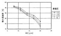
上記の説明においては、OS駆動方法を適用した場合に優れた動画表示性能を有する配向分割垂直配向型LCDの構成(特に、液晶領域幅W3の幅)を説明するために、黒電圧の影響については説明しなかった。例えば、図6の極小透過率の液晶領域幅W3依存性を示すグラフは、典型的な例として黒電圧を1.2Vとした場合の結果を示している。 In the above description, in order to explain the configuration of an alignment-divided vertical alignment LCD (particularly the width of the liquid crystal region width W3) having excellent moving image display performance when the OS driving method is applied, the influence of the black voltage is described. Did not explain. For example, the graph showing the dependence of the minimum transmittance on the liquid crystal region width W3 in FIG. 6 shows the result when the black voltage is 1.2 V as a typical example.
ここで、図18および図19を参照しながら、黒電圧が極小透過率の液晶領域幅W3依存性に与える影響を説明する。ここで用いたLCDのセルパラメータは表7に示す通りであり、パネル表面温度が25℃における測定結果を示している。白電圧はいずれも7.6Vとした。図18は0階調から32階調への表示を切替える際のOS電圧印加後に表れる極小透過率を、32階調の透過率を100%として表しており、図19は、0階調から64階調への表示を切替える際のOS電圧印加後に表れる極小透過率を、64階調の透過率を100%として表している。なお、いずれの液晶層についても、液晶材料は、回転粘度γ1が約133mPa・s、フロー粘度νが約19mm2/sであり、且つ、それぞれの液晶層のリタデーション(厚さd×複屈折率Δn)が約300nmとなるように液晶材料を選んだ。Here, the influence of the black voltage on the dependence of the minimum transmittance on the liquid crystal region width W3 will be described with reference to FIGS. The cell parameters of the LCD used here are as shown in Table 7, and show the measurement results when the panel surface temperature is 25 ° C. The white voltages were all 7.6V. FIG. 18 shows the minimum transmittance that appears after application of the OS voltage when switching the display from the 0 gradation to the 32 gradation, assuming that the transmittance at the 32 gradation is 100%, and FIG. The minimum transmittance that appears after the application of the OS voltage when switching the display to gradation is represented with the transmittance of 64 gradations being 100%. In any liquid crystal layer, the liquid crystal material has a rotational viscosity γ1 of about 133 mPa · s, a flow viscosity ν of about 19 mm2 / s, and the retardation (thickness d × birefringence index) of each liquid crystal layer. The liquid crystal material was selected so that Δn) was about 300 nm.
図18および図19からわかるように、全ての液晶領域幅W3について、黒電圧が高いほど極小透過率が高い。すなわち、動画表示性能を改善するためには黒電圧を高く設定することが好ましい。これは、黒電圧が高いほど、斜め電界による配向規制力が強くなり、液晶分子の傾斜角が大きくなるためである。このことから容易にわかるように、黒電圧を高くするとと透過率が高くなる。従って、高いコントラスト比を得るためには、黒電圧は低い方が好ましいことになる。液晶領域幅W3が11μmで、黒電圧が0V、0.5V、1.0Vおよび1.6Vのときのコントラスト比は、順に657、613、573および539であった。 As can be seen from FIGS. 18 and 19, for all liquid crystal region widths W3, the minimum transmittance is higher as the black voltage is higher. That is, it is preferable to set the black voltage high in order to improve the moving image display performance. This is because the higher the black voltage, the stronger the alignment regulating force due to the oblique electric field and the larger the tilt angle of the liquid crystal molecules. As can be easily understood from this, when the black voltage is increased, the transmittance is increased. Therefore, in order to obtain a high contrast ratio, a lower black voltage is preferable. The contrast ratios when the liquid crystal region width W3 was 11 μm and the black voltages were 0V, 0.5V, 1.0V, and 1.6V were 657, 613, 573, and 539, respectively.
図18をみると、液晶領域幅W3を14μm以下とすれば、黒電圧を0Vとしても、80%以上の極小透過率を得ることができ、図19においては、85%を超える極小透過率を得ることができる。さらに、液晶領域幅W3を12μm以下にすれば、図18において約85%以上の極小透過率が得られ、図19においては90%以上の極小透過率を得ることができる。 As shown in FIG. 18, when the liquid crystal region width W3 is 14 μm or less, a minimum transmittance of 80% or more can be obtained even when the black voltage is set to 0 V. In FIG. 19, a minimum transmittance exceeding 85% is obtained. Can be obtained. Further, if the liquid crystal region width W3 is set to 12 μm or less, a minimum transmittance of about 85% or more can be obtained in FIG. 18, and a minimum transmittance of 90% or more can be obtained in FIG.
このように、本発明の実施形態によると、動画表示性能に優れた構成が得られるので、黒電圧を従来よりも低く設定しても従来と同等以上の動画表示性能を得ることができる。すなわち、動画表示性能を犠牲にすることなく、コントラスト比を向上することも可能となる。なお、動画表示性能やコントラスト比はLCDの用途によって要求されるレベルが異なるので、適宜最適化すればよい。 As described above, according to the embodiment of the present invention, a configuration excellent in moving image display performance can be obtained. Therefore, even when the black voltage is set lower than that in the past, a moving image display performance equal to or higher than that in the past can be obtained. That is, the contrast ratio can be improved without sacrificing the moving image display performance. It should be noted that the moving image display performance and the contrast ratio have different levels depending on the application of the LCD, and may be optimized as appropriate.
本発明によると、MVA型やCPA型などの広視野角特性を有する配向分割垂直配向型LCDの応答特性が改善され、高品位の動画表示が可能なLCDが提供される。特に、配向分割垂直配向型LCDにOS駆動を適用しても、角応答に起因する表示品位の低下が発生せず、高品位の動画表示が可能なLCDが提供される。本発明によるLCDは、テレビジョンを始め種々の用途に適用される。 According to the present invention, the response characteristics of an alignment division vertical alignment type LCD having a wide viewing angle characteristic such as an MVA type or a CPA type are improved, and an LCD capable of displaying a high-quality moving image is provided. In particular, even when OS driving is applied to an alignment-divided vertical alignment LCD, an LCD capable of displaying a high-quality moving image without causing a deterioration in display quality due to angular response is provided. The LCD according to the present invention is applied to various uses including television.
11 第1電極
12 第2電極
13 液晶層
13A 液晶領域
13a 液晶分子
21 第1配向規制手段(リブ)
22 第2配向規制手段(スリット)DESCRIPTION OF
22 Second orientation regulating means (slit)
Claims (23)
Translated fromJapanese前記液晶層の前記第1電極側に設けられ、第1の幅を有する第1配向規制手段と、
前記液晶層の前記第2電極側に設けられ、第2の幅を有する第2配向規制手段と、
前記第1配向規制手段と前記第2配向規制手段との間に規定され、第3の幅を有する液晶領域とを有し、前記第3の幅が2μm以上14μm以下である、液晶表示装置。Each includes a plurality of pixels having a first electrode, a second electrode facing the first electrode, and a vertical alignment type liquid crystal layer provided between the first electrode and the second electrode,
A first alignment regulating means provided on the first electrode side of the liquid crystal layer and having a first width;
A second alignment regulating means provided on the second electrode side of the liquid crystal layer and having a second width;
A liquid crystal display device having a liquid crystal region having a third width defined between the first alignment regulating means and the second alignment regulating means, wherein the third width is 2 μm or more and 14 μm or less.
前記液晶層の前記第1電極側に設けられ、第1の幅を有する第1配向規制手段と、
前記液晶層の前記第2電極側に設けられ、第2の幅を有する第2配向規制手段と、
前記第1配向規制手段と前記第2配向規制手段との間に規定され、第3の幅を有する液晶領域とを有し、
前記液晶領域は、前記第1配向規制手段に隣接し第1の応答速度を有する第1液晶領域と、前記第2配向規制手段に隣接し第2の応答速度を有する第2液晶領域と、前記第1液晶領域と前記第2液晶領域との間に規定され、前記第1および第2の応答速度よりも遅い第3の応答速度を有する第3液晶領域とを有し、
前記第3液晶領域内において、黒表示状態から1垂直走査期間に32/255階調の透過率に到達する電圧を印加した後1垂直走査期間に相当する時間が経過したときの透過率が黒表示状態の透過率の2倍以下の領域の幅が2μm以下である、液晶表示装置。Each includes a plurality of pixels having a first electrode, a second electrode facing the first electrode, and a vertical alignment type liquid crystal layer provided between the first electrode and the second electrode,
A first alignment regulating means provided on the first electrode side of the liquid crystal layer and having a first width;
A second alignment regulating means provided on the second electrode side of the liquid crystal layer and having a second width;
A liquid crystal region defined between the first alignment regulating means and the second alignment regulating means and having a third width;
The liquid crystal region includes a first liquid crystal region having a first response speed adjacent to the first alignment restriction means, a second liquid crystal region having a second response speed adjacent to the second alignment restriction means, A third liquid crystal region defined between the first liquid crystal region and the second liquid crystal region and having a third response speed slower than the first and second response speeds;
In the third liquid crystal region, the transmittance is black when a time corresponding to one vertical scanning period has elapsed after applying a voltage that reaches the transmittance of 32/255 gradation in one vertical scanning period from the black display state. A liquid crystal display device, wherein the width of a region that is twice or less the transmittance in a display state is 2 μm or less.
前記液晶層の前記第1電極側に設けられ、第1の幅を有する帯状の第1配向規制手段と、前記液晶層の前記第2電極側に設けられ、第2の幅を有する帯状の第2配向規制手段と、前記第1配向規制手段と前記第2配向規制手段との間に規定され、第3の幅を有する帯状の液晶領域とを有し、
前記第3の幅が2μm以上14μm以下であって、前記液晶層の厚さが3μm未満である、液晶表示装置。Each includes a plurality of pixels having a first electrode, a second electrode facing the first electrode, and a vertical alignment type liquid crystal layer provided between the first electrode and the second electrode,
A strip-shaped first alignment regulating means having a first width provided on the first electrode side of the liquid crystal layer, and a strip-shaped first strip having a second width provided on the second electrode side of the liquid crystal layer. 2 alignment regulating means, a band-shaped liquid crystal region having a third width defined between the first alignment regulating means and the second alignment regulating means,
The liquid crystal display device, wherein the third width is 2 μm or more and 14 μm or less, and the thickness of the liquid crystal layer is less than 3 μm.
Priority Applications (7)
| Application Number | Priority Date | Filing Date | Title |
|---|---|---|---|
| JP2004205103AJP2005055880A (en) | 2003-07-24 | 2004-07-12 | Liquid crystal display device and driving method thereof |
| KR1020040057658AKR100680102B1 (en) | 2003-07-24 | 2004-07-23 | LCD and its driving method |
| TW093122214ATWI286260B (en) | 2003-07-24 | 2004-07-23 | Liquid crystal display device and driving method for the same |
| CNB2004100589544ACN1318891C (en) | 2003-07-24 | 2004-07-23 | Liquid crystal display device and driving circuit thereof |
| US10/898,688US7292301B2 (en) | 2003-07-24 | 2004-07-26 | Liquid crystal display device and driving method for the same |
| KR1020060115644AKR101120289B1 (en) | 2003-07-24 | 2006-11-22 | Liquid crystal display device and driving method for the same |
| KR1020100024036AKR100988990B1 (en) | 2003-07-24 | 2010-03-18 | Liquid crystal display device and driving method for the same |
Applications Claiming Priority (2)
| Application Number | Priority Date | Filing Date | Title |
|---|---|---|---|
| JP2003279083 | 2003-07-24 | ||
| JP2004205103AJP2005055880A (en) | 2003-07-24 | 2004-07-12 | Liquid crystal display device and driving method thereof |
Publications (1)
| Publication Number | Publication Date |
|---|---|
| JP2005055880Atrue JP2005055880A (en) | 2005-03-03 |
Family
ID=34106891
Family Applications (1)
| Application Number | Title | Priority Date | Filing Date |
|---|---|---|---|
| JP2004205103APendingJP2005055880A (en) | 2003-07-24 | 2004-07-12 | Liquid crystal display device and driving method thereof |
Country Status (5)
| Country | Link |
|---|---|
| US (1) | US7292301B2 (en) |
| JP (1) | JP2005055880A (en) |
| KR (3) | KR100680102B1 (en) |
| CN (1) | CN1318891C (en) |
| TW (1) | TWI286260B (en) |
Cited By (5)
| Publication number | Priority date | Publication date | Assignee | Title |
|---|---|---|---|---|
| JP2006330605A (en)* | 2005-05-30 | 2006-12-07 | Sharp Corp | Liquid crystal display |
| JPWO2008035471A1 (en)* | 2006-09-22 | 2010-01-28 | シャープ株式会社 | Liquid crystal display |
| US11373595B2 (en) | 2020-07-30 | 2022-06-28 | Joled Inc. | Display device and method for driving display device |
| US11450278B2 (en) | 2020-09-09 | 2022-09-20 | Joled Inc. | Display device and display device driving method |
| US11568812B2 (en) | 2020-09-03 | 2023-01-31 | Joled Inc. | Display device and display device driving method |
Families Citing this family (13)
| Publication number | Priority date | Publication date | Assignee | Title |
|---|---|---|---|---|
| JP2005265891A (en)* | 2004-03-16 | 2005-09-29 | Sharp Corp | Liquid crystal display device and driving method thereof |
| KR100984363B1 (en)* | 2004-03-31 | 2010-09-30 | 삼성전자주식회사 | Liquid crystal display and fabricating method thereof |
| JP4015157B2 (en)* | 2004-07-20 | 2007-11-28 | シャープ株式会社 | Drive device for liquid crystal display device, program and recording medium, and liquid crystal display device |
| KR101112564B1 (en)* | 2005-01-18 | 2012-03-13 | 삼성전자주식회사 | Liquid crystal display device |
| US8217880B2 (en) | 2005-03-31 | 2012-07-10 | Sharp Kabushiki Kaisha | Method for driving liquid crystal display apparatus |
| US8264441B2 (en) | 2005-03-31 | 2012-09-11 | Sharp Kabushiki Kaisha | Method for driving liquid crystal display apparatus |
| TWI304906B (en)* | 2005-06-17 | 2009-01-01 | Au Optronics Corp | A va type liquid crystal display |
| CN100538481C (en)* | 2005-12-28 | 2009-09-09 | 友达光电股份有限公司 | pixel structure |
| US8184221B2 (en) | 2006-12-25 | 2012-05-22 | Sharp Kabushiki Kaisha | Liquid crystal display panel, liquid crystal display element, and liquid crystal display device |
| JP4609468B2 (en)* | 2007-09-20 | 2011-01-12 | カシオ計算機株式会社 | Display device and display driving method thereof |
| JP5307230B2 (en)* | 2009-04-03 | 2013-10-02 | シャープ株式会社 | Liquid crystal display |
| JP2014191109A (en)* | 2013-03-26 | 2014-10-06 | Japan Display Inc | Liquid crystal display device and electronic apparatus |
| CN111201561B (en)* | 2017-10-30 | 2021-08-13 | 华为技术有限公司 | Luminance Attenuation Estimation |
Citations (6)
| Publication number | Priority date | Publication date | Assignee | Title |
|---|---|---|---|---|
| JPH11242225A (en)* | 1997-06-12 | 1999-09-07 | Fujitsu Ltd | Liquid crystal display |
| JPH11352489A (en)* | 1998-05-16 | 1999-12-24 | Samsung Electronics Co Ltd | Wide viewing angle liquid crystal display device and method of manufacturing the same |
| JP2000231091A (en)* | 1998-12-08 | 2000-08-22 | Fujitsu Ltd | Liquid crystal display device and driving method thereof |
| JP2001281664A (en)* | 2000-03-30 | 2001-10-10 | Fujitsu Ltd | Liquid crystal display |
| JP2002055343A (en)* | 2000-02-25 | 2002-02-20 | Sharp Corp | Liquid crystal display |
| JP2002202511A (en)* | 2000-10-31 | 2002-07-19 | Sharp Corp | Liquid crystal display |
Family Cites Families (13)
| Publication number | Priority date | Publication date | Assignee | Title |
|---|---|---|---|---|
| US159018A (en)* | 1875-01-26 | Improvement in paper-ruling machines | ||
| US40546A (en)* | 1863-11-10 | Improvement in polishing-machines | ||
| JP2839085B2 (en)* | 1996-07-25 | 1998-12-16 | 日本電気株式会社 | Liquid crystal display |
| KR100283511B1 (en)* | 1998-05-20 | 2001-03-02 | 윤종용 | Wide viewing angle liquid crystal display |
| JP3926056B2 (en)* | 1999-03-16 | 2007-06-06 | シャープ株式会社 | Liquid crystal display |
| JP2001013889A (en)* | 1999-06-29 | 2001-01-19 | Toshiba Corp | Flat panel display |
| JP4553283B2 (en)* | 2000-08-25 | 2010-09-29 | インターナショナル・ビジネス・マシーンズ・コーポレーション | Holding frame and image display device |
| JP3877129B2 (en) | 2000-09-27 | 2007-02-07 | シャープ株式会社 | Liquid crystal display |
| JP3992922B2 (en)* | 2000-11-27 | 2007-10-17 | シャープ株式会社 | LIQUID CRYSTAL DISPLAY SUBSTRATE, ITS MANUFACTURING METHOD, AND LIQUID CRYSTAL DISPLAY DEVICE EQUIPPED WITH THE SAME |
| US6977704B2 (en)* | 2001-03-30 | 2005-12-20 | Fujitsu Display Technologies Corporation | Liquid crystal display |
| JP3989238B2 (en)* | 2001-12-07 | 2007-10-10 | シャープ株式会社 | Liquid crystal display |
| KR20040008920A (en) | 2002-07-19 | 2004-01-31 | 삼성전자주식회사 | A vertically aligned mode liquid crystal display |
| JP2005084237A (en)* | 2003-09-05 | 2005-03-31 | Sharp Corp | Liquid crystal display |
- 2004
- 2004-07-12JPJP2004205103Apatent/JP2005055880A/enactivePending
- 2004-07-23KRKR1020040057658Apatent/KR100680102B1/ennot_activeExpired - Fee Related
- 2004-07-23TWTW093122214Apatent/TWI286260B/ennot_activeIP Right Cessation
- 2004-07-23CNCNB2004100589544Apatent/CN1318891C/ennot_activeExpired - Fee Related
- 2004-07-26USUS10/898,688patent/US7292301B2/ennot_activeExpired - Lifetime
- 2006
- 2006-11-22KRKR1020060115644Apatent/KR101120289B1/ennot_activeExpired - Fee Related
- 2010
- 2010-03-18KRKR1020100024036Apatent/KR100988990B1/ennot_activeExpired - Fee Related
Patent Citations (6)
| Publication number | Priority date | Publication date | Assignee | Title |
|---|---|---|---|---|
| JPH11242225A (en)* | 1997-06-12 | 1999-09-07 | Fujitsu Ltd | Liquid crystal display |
| JPH11352489A (en)* | 1998-05-16 | 1999-12-24 | Samsung Electronics Co Ltd | Wide viewing angle liquid crystal display device and method of manufacturing the same |
| JP2000231091A (en)* | 1998-12-08 | 2000-08-22 | Fujitsu Ltd | Liquid crystal display device and driving method thereof |
| JP2002055343A (en)* | 2000-02-25 | 2002-02-20 | Sharp Corp | Liquid crystal display |
| JP2001281664A (en)* | 2000-03-30 | 2001-10-10 | Fujitsu Ltd | Liquid crystal display |
| JP2002202511A (en)* | 2000-10-31 | 2002-07-19 | Sharp Corp | Liquid crystal display |
Cited By (6)
| Publication number | Priority date | Publication date | Assignee | Title |
|---|---|---|---|---|
| JP2006330605A (en)* | 2005-05-30 | 2006-12-07 | Sharp Corp | Liquid crystal display |
| JPWO2008035471A1 (en)* | 2006-09-22 | 2010-01-28 | シャープ株式会社 | Liquid crystal display |
| US8432520B2 (en) | 2006-09-22 | 2013-04-30 | Sharp Kabushiki Kaisha | Liquid crystal display device |
| US11373595B2 (en) | 2020-07-30 | 2022-06-28 | Joled Inc. | Display device and method for driving display device |
| US11568812B2 (en) | 2020-09-03 | 2023-01-31 | Joled Inc. | Display device and display device driving method |
| US11450278B2 (en) | 2020-09-09 | 2022-09-20 | Joled Inc. | Display device and display device driving method |
Also Published As
| Publication number | Publication date |
|---|---|
| KR20070001850A (en) | 2007-01-04 |
| KR100988990B1 (en) | 2010-10-20 |
| US7292301B2 (en) | 2007-11-06 |
| TW200515077A (en) | 2005-05-01 |
| TWI286260B (en) | 2007-09-01 |
| US20050024546A1 (en) | 2005-02-03 |
| CN1576976A (en) | 2005-02-09 |
| CN1318891C (en) | 2007-05-30 |
| KR20100033996A (en) | 2010-03-31 |
| KR100680102B1 (en) | 2007-02-09 |
| KR101120289B1 (en) | 2012-03-06 |
| KR20050012178A (en) | 2005-01-31 |
Similar Documents
| Publication | Publication Date | Title |
|---|---|---|
| KR101120289B1 (en) | Liquid crystal display device and driving method for the same | |
| JP2005292515A (en) | Liquid crystal display device, driving method thereof, and electronic apparatus | |
| JP4571855B2 (en) | Substrate for liquid crystal display device, liquid crystal display device including the same, and driving method thereof | |
| CN100507689C (en) | Liquid crystal display and its driving method | |
| JP2005084237A (en) | Liquid crystal display | |
| KR100693958B1 (en) | Liquid crystal display, its driving method and electronic device | |
| JP2005265891A (en) | Liquid crystal display device and driving method thereof | |
| CN100378550C (en) | Liquid crystal display, driving method thereof, and electronic device | |
| JP2010198043A (en) | Liquid crystal display | |
| US6822700B2 (en) | Liquid crystal display device having stairs type driving signal | |
| JP2005250361A (en) | Liquid crystal display | |
| JP2006201594A (en) | Liquid crystal display | |
| JP4662947B2 (en) | Liquid crystal display device and electronic apparatus including the same | |
| KR100948614B1 (en) | Liquid crystal material having enhanced response time, liquid crystal display apparatus having the same, and method of manufacturing the liquid crystal display apparatus |
Legal Events
| Date | Code | Title | Description |
|---|---|---|---|
| A621 | Written request for application examination | Free format text:JAPANESE INTERMEDIATE CODE: A621 Effective date:20060912 | |
| A977 | Report on retrieval | Free format text:JAPANESE INTERMEDIATE CODE: A971007 Effective date:20090402 | |
| A131 | Notification of reasons for refusal | Free format text:JAPANESE INTERMEDIATE CODE: A131 Effective date:20091208 | |
| A521 | Written amendment | Free format text:JAPANESE INTERMEDIATE CODE: A523 Effective date:20100204 | |
| A02 | Decision of refusal | Free format text:JAPANESE INTERMEDIATE CODE: A02 Effective date:20100316 |