JP2005051252A - Method for manufacturing semiconductor device - Google Patents
Method for manufacturing semiconductor deviceDownload PDFInfo
- Publication number
- JP2005051252A JP2005051252AJP2004242135AJP2004242135AJP2005051252AJP 2005051252 AJP2005051252 AJP 2005051252AJP 2004242135 AJP2004242135 AJP 2004242135AJP 2004242135 AJP2004242135 AJP 2004242135AJP 2005051252 AJP2005051252 AJP 2005051252A
- Authority
- JP
- Japan
- Prior art keywords
- silicon film
- film
- substrate
- polycrystalline silicon
- amorphous silicon
- Prior art date
- Legal status (The legal status is an assumption and is not a legal conclusion. Google has not performed a legal analysis and makes no representation as to the accuracy of the status listed.)
- Pending
Links
- 238000000034methodMethods0.000titleclaimsabstractdescription120
- 238000004519manufacturing processMethods0.000titleclaimsabstractdescription57
- 239000004065semiconductorSubstances0.000titleclaimsabstractdescription29
- 229910021420polycrystalline siliconInorganic materials0.000claimsabstractdescription88
- 239000000758substrateSubstances0.000claimsabstractdescription67
- 229910021417amorphous siliconInorganic materials0.000claimsabstractdescription64
- 239000012535impuritySubstances0.000claimsabstractdescription52
- 238000010438heat treatmentMethods0.000claimsabstractdescription31
- 238000004151rapid thermal annealingMethods0.000claimsdescription30
- 238000005224laser annealingMethods0.000claimsdescription26
- 238000000137annealingMethods0.000claimsdescription18
- 230000003213activating effectEffects0.000claimsdescription7
- 229910052724xenonInorganic materials0.000claimsdescription6
- FHNFHKCVQCLJFQ-UHFFFAOYSA-Nxenon atomChemical compound[Xe]FHNFHKCVQCLJFQ-UHFFFAOYSA-N0.000claimsdescription6
- 230000001678irradiating effectEffects0.000claimsdescription4
- FVBUAEGBCNSCDD-UHFFFAOYSA-Nsilicide(4-)Chemical compound[Si-4]FVBUAEGBCNSCDD-UHFFFAOYSA-N0.000abstractdescription39
- 229910021332silicideInorganic materials0.000abstractdescription38
- 239000011521glassSubstances0.000abstractdescription7
- XUIMIQQOPSSXEZ-UHFFFAOYSA-NSiliconChemical compound[Si]XUIMIQQOPSSXEZ-UHFFFAOYSA-N0.000abstractdescription4
- 229910052710siliconInorganic materials0.000abstractdescription4
- 239000010703siliconSubstances0.000abstractdescription4
- 239000010408filmSubstances0.000description229
- VYPSYNLAJGMNEJ-UHFFFAOYSA-NSilicium dioxideChemical compoundO=[Si]=OVYPSYNLAJGMNEJ-UHFFFAOYSA-N0.000description33
- 229910052814silicon oxideInorganic materials0.000description30
- 239000010410layerSubstances0.000description18
- 238000000151depositionMethods0.000description17
- 239000010409thin filmSubstances0.000description17
- 239000004973liquid crystal related substanceSubstances0.000description15
- 230000004913activationEffects0.000description13
- 210000002858crystal cellAnatomy0.000description13
- 239000003990capacitorSubstances0.000description10
- 238000004518low pressure chemical vapour depositionMethods0.000description10
- 238000001312dry etchingMethods0.000description9
- 238000000206photolithographyMethods0.000description9
- BOTDANWDWHJENH-UHFFFAOYSA-NTetraethyl orthosilicateChemical compoundCCO[Si](OCC)(OCC)OCCBOTDANWDWHJENH-UHFFFAOYSA-N0.000description8
- 230000008021depositionEffects0.000description8
- 239000007789gasSubstances0.000description8
- 238000004544sputter depositionMethods0.000description8
- 238000001505atmospheric-pressure chemical vapour depositionMethods0.000description7
- 239000007790solid phaseSubstances0.000description7
- QGZKDVFQNNGYKY-UHFFFAOYSA-NAmmoniaChemical compoundNQGZKDVFQNNGYKY-UHFFFAOYSA-N0.000description6
- BLRPTPMANUNPDV-UHFFFAOYSA-NSilaneChemical group[SiH4]BLRPTPMANUNPDV-UHFFFAOYSA-N0.000description6
- 239000013081microcrystalSubstances0.000description6
- 229910004298SiO 2Inorganic materials0.000description5
- 239000013078crystalSubstances0.000description5
- 238000002425crystallisationMethods0.000description5
- 230000008025crystallizationEffects0.000description5
- 238000010586diagramMethods0.000description5
- 150000002500ionsChemical class0.000description5
- 239000000203mixtureSubstances0.000description5
- 230000002093peripheral effectEffects0.000description5
- 238000003860storageMethods0.000description5
- IJGRMHOSHXDMSA-UHFFFAOYSA-NAtomic nitrogenChemical compoundN#NIJGRMHOSHXDMSA-UHFFFAOYSA-N0.000description4
- CPELXLSAUQHCOX-UHFFFAOYSA-NHydrogen bromideChemical compoundBrCPELXLSAUQHCOX-UHFFFAOYSA-N0.000description4
- 238000005229chemical vapour depositionMethods0.000description4
- 230000000694effectsEffects0.000description4
- 239000011229interlayerSubstances0.000description4
- 239000003870refractory metalSubstances0.000description4
- OAICVXFJPJFONN-UHFFFAOYSA-NPhosphorusChemical compound[P]OAICVXFJPJFONN-UHFFFAOYSA-N0.000description3
- 238000010521absorption reactionMethods0.000description3
- 229910021529ammoniaInorganic materials0.000description3
- 238000009792diffusion processMethods0.000description3
- 239000011159matrix materialSubstances0.000description3
- 230000003287optical effectEffects0.000description3
- UPSOBXZLFLJAKK-UHFFFAOYSA-Nozone;tetraethyl silicateChemical compound[O-][O+]=O.CCO[Si](OCC)(OCC)OCCUPSOBXZLFLJAKK-UHFFFAOYSA-N0.000description3
- 229910052698phosphorusInorganic materials0.000description3
- 239000011574phosphorusSubstances0.000description3
- 238000005268plasma chemical vapour depositionMethods0.000description3
- 230000003405preventing effectEffects0.000description3
- 238000012545processingMethods0.000description3
- 229910019001CoSiInorganic materials0.000description2
- 229910016006MoSiInorganic materials0.000description2
- 229910008484TiSiInorganic materials0.000description2
- 230000001133accelerationEffects0.000description2
- 229910045601alloyInorganic materials0.000description2
- 239000000956alloySubstances0.000description2
- QVGXLLKOCUKJST-UHFFFAOYSA-Natomic oxygenChemical compound[O]QVGXLLKOCUKJST-UHFFFAOYSA-N0.000description2
- 229910052804chromiumInorganic materials0.000description2
- 230000007423decreaseEffects0.000description2
- 230000007547defectEffects0.000description2
- 238000011161developmentMethods0.000description2
- PZPGRFITIJYNEJ-UHFFFAOYSA-NdisilaneChemical compound[SiH3][SiH3]PZPGRFITIJYNEJ-UHFFFAOYSA-N0.000description2
- 238000009826distributionMethods0.000description2
- 238000010894electron beam technologyMethods0.000description2
- 239000001257hydrogenSubstances0.000description2
- 229910052739hydrogenInorganic materials0.000description2
- 229910000042hydrogen bromideInorganic materials0.000description2
- 238000005984hydrogenation reactionMethods0.000description2
- 239000000463materialSubstances0.000description2
- 229910052751metalInorganic materials0.000description2
- 239000002184metalSubstances0.000description2
- 238000001451molecular beam epitaxyMethods0.000description2
- 229910052750molybdenumInorganic materials0.000description2
- 238000005121nitridingMethods0.000description2
- 229910052757nitrogenInorganic materials0.000description2
- -1nitrogen ionsChemical class0.000description2
- 239000001301oxygenSubstances0.000description2
- 229910052760oxygenInorganic materials0.000description2
- 239000002245particleSubstances0.000description2
- 238000005240physical vapour depositionMethods0.000description2
- 238000009832plasma treatmentMethods0.000description2
- 230000001681protective effectEffects0.000description2
- 238000005979thermal decomposition reactionMethods0.000description2
- 229910052719titaniumInorganic materials0.000description2
- 229910052721tungstenInorganic materials0.000description2
- 238000007740vapor depositionMethods0.000description2
- 229910021364Al-Si alloyInorganic materials0.000description1
- ZOXJGFHDIHLPTG-UHFFFAOYSA-NBoronChemical compound[B]ZOXJGFHDIHLPTG-UHFFFAOYSA-N0.000description1
- KZBUYRJDOAKODT-UHFFFAOYSA-NChlorineChemical compoundClClKZBUYRJDOAKODT-UHFFFAOYSA-N0.000description1
- UFHFLCQGNIYNRP-UHFFFAOYSA-NHydrogenChemical compound[H][H]UFHFLCQGNIYNRP-UHFFFAOYSA-N0.000description1
- CBENFWSGALASAD-UHFFFAOYSA-NOzoneChemical compound[O-][O+]=OCBENFWSGALASAD-UHFFFAOYSA-N0.000description1
- 229910052581Si3N4Inorganic materials0.000description1
- 229910001069Ti alloyInorganic materials0.000description1
- 230000002411adverseEffects0.000description1
- 239000003513alkaliSubstances0.000description1
- 238000013459approachMethods0.000description1
- 238000000149argon plasma sinteringMethods0.000description1
- 229910052785arsenicInorganic materials0.000description1
- RQNWIZPPADIBDY-UHFFFAOYSA-Narsenic atomChemical compound[As]RQNWIZPPADIBDY-UHFFFAOYSA-N0.000description1
- 230000015572biosynthetic processEffects0.000description1
- 229910052796boronInorganic materials0.000description1
- 229910052799carbonInorganic materials0.000description1
- 210000004027cellAnatomy0.000description1
- 238000006243chemical reactionMethods0.000description1
- 239000000460chlorineSubstances0.000description1
- 239000000470constituentSubstances0.000description1
- 229910021419crystalline siliconInorganic materials0.000description1
- 230000006866deteriorationEffects0.000description1
- 238000005530etchingMethods0.000description1
- 238000002474experimental methodMethods0.000description1
- 230000005669field effectEffects0.000description1
- 229910052737goldInorganic materials0.000description1
- 150000002431hydrogenChemical class0.000description1
- 125000004435hydrogen atomChemical group[H]*0.000description1
- 230000006698inductionEffects0.000description1
- 238000007737ion beam depositionMethods0.000description1
- 238000007733ion platingMethods0.000description1
- 238000010884ion-beam techniqueMethods0.000description1
- 238000001755magnetron sputter depositionMethods0.000description1
- 230000008018meltingEffects0.000description1
- 238000002844meltingMethods0.000description1
- 150000004767nitridesChemical class0.000description1
- 239000010453quartzSubstances0.000description1
- 238000004904shorteningMethods0.000description1
- 229910000077silaneInorganic materials0.000description1
- HQVNEWCFYHHQES-UHFFFAOYSA-Nsilicon nitrideChemical compoundN12[Si]34N5[Si]62N3[Si]51N64HQVNEWCFYHHQES-UHFFFAOYSA-N0.000description1
- 239000007787solidSubstances0.000description1
- 239000007858starting materialSubstances0.000description1
- 230000003068static effectEffects0.000description1
- 239000000126substanceSubstances0.000description1
- 230000001360synchronised effectEffects0.000description1
- 229910052715tantalumInorganic materials0.000description1
- 238000002834transmittanceMethods0.000description1
- WQJQOUPTWCFRMM-UHFFFAOYSA-Ntungsten disilicideChemical compound[Si]#[W]#[Si]WQJQOUPTWCFRMM-UHFFFAOYSA-N0.000description1
- NXHILIPIEUBEPD-UHFFFAOYSA-Htungsten hexafluorideChemical compoundF[W](F)(F)(F)(F)FNXHILIPIEUBEPD-UHFFFAOYSA-H0.000description1
- 229910021342tungsten silicideInorganic materials0.000description1
- 238000001771vacuum depositionMethods0.000description1
Images


Landscapes
- Recrystallisation Techniques (AREA)
- Electrodes Of Semiconductors (AREA)
- Thin Film Transistor (AREA)
Abstract
Description
Translated fromJapanese本発明は、薄膜トランジスタ(Thin Film Transistor)等の半導体装置の製造方法に関するものである。 The present invention relates to a method for manufacturing a semiconductor device such as a thin film transistor.
近年、アクティブマトリクス方式LCD(Liqid Crystal Display)の画素駆動素子(画素駆動用トランジスタ)として、透明絶縁基板上に形成された多結晶シリコン膜を能動層に用いた薄膜トランジスタ(以下、多結晶シリコンTFTという)の開発が進められている。 In recent years, as a pixel driving element (pixel driving transistor) of an active matrix LCD (Liqid Crystal Display), a thin film transistor (hereinafter referred to as a polycrystalline silicon TFT) using a polycrystalline silicon film formed on a transparent insulating substrate as an active layer. ) Is under development.
多結晶シリコンTFTは、非晶質シリコン膜を能動層に用いた薄膜トランジスタに比べ、移動度が大きく駆動能力が高いという利点がある。そのため、多結晶シリコンTFTを用いれば、高性能なLCDを実現できる上に、画素部(表示部)だけでなく周辺駆動回路(ドライバ部)までを同一基板上に一体に形成することができる。 Polycrystalline silicon TFTs have the advantage of higher mobility and higher driving capability than thin film transistors using amorphous silicon films as active layers. Therefore, if a polycrystalline silicon TFT is used, a high-performance LCD can be realized, and not only the pixel portion (display portion) but also the peripheral drive circuit (driver portion) can be integrally formed on the same substrate.
このような多結晶シリコンTFTにおいて、能動層としての多結晶シリコン膜の形成方法としては、基板上に直接多結晶シリコン膜を堆積させる方法や基板上に非晶質シリコン膜を形成した後に、これを多結晶化する方法等がある。このうち、多結晶シリコン膜を直接基板に堆積させる方法は、例えば、CVD法を用い、高温下で堆積させるという比較的簡単な工程である。 In such a polycrystalline silicon TFT, as a method of forming a polycrystalline silicon film as an active layer, a method of depositing a polycrystalline silicon film directly on a substrate or an amorphous silicon film formed on a substrate is used. There is a method of polycrystallizing. Among these, the method of depositing the polycrystalline silicon film directly on the substrate is a relatively simple process of depositing at a high temperature using, for example, a CVD method.
また、非晶質シリコン膜を堆積した後にこれを多結晶化するには、固相成長法が一般的である。この固相成長法は、非晶質シリコン膜に熱処理を行うことにより、固体のままで多結晶化させて多結晶シリコン膜を得る方法である。この固相成長法の一例を図31及び図32に基づいて説明する。 In order to polycrystallize an amorphous silicon film after it is deposited, a solid phase growth method is generally used. This solid phase growth method is a method in which a polycrystalline silicon film is obtained by performing heat treatment on an amorphous silicon film to be polycrystallized in a solid state. An example of this solid phase growth method will be described with reference to FIGS.
工程A(図31参照):絶縁基板(例えば石英ガラス)61上に、通常の減圧CVD法を用いて非晶質シリコン膜を形成し、更に、窒素(N2)雰囲気中、温度900℃程度で熱処理を行うことにより、前記非晶質シリコン膜を固相成長させて多結晶シリコン膜62を形成する。Step A (see FIG. 31): An amorphous silicon film is formed on an insulating substrate (for example, quartz glass) 61 by using a normal low pressure CVD method. Further, in a nitrogen (N2 ) atmosphere, a temperature of about 900 ° C. The amorphous silicon film is solid-phase grown by performing a heat treatment in order to form a polycrystalline silicon film 62.
前記多結晶シリコン膜62を薄膜トランジスタの能動層として用いるために、フォトリソグラフィ技術、RIE法によるドライエッチング技術により前記多結晶シリコン膜62を所定形状に加工する。 In order to use the polycrystalline silicon film 62 as an active layer of a thin film transistor, the polycrystalline silicon film 62 is processed into a predetermined shape by a photolithography technique or a dry etching technique by RIE.
前記多結晶シリコン膜62の上に、減圧CVD法を用いて、ゲート絶縁膜63としてのシリコン酸化膜を堆積する。 A silicon oxide film as a gate insulating film 63 is deposited on the polycrystalline silicon film 62 by using a low pressure CVD method.
工程B(図32参照):前記ゲート絶縁膜63上に、減圧CVD法により多結晶シリコン膜を堆積した後、この多結晶シリコン膜に不純物を注入し、更に熱処理を行って不純物を活性化させる。 Step B (see FIG. 32): After depositing a polycrystalline silicon film on the gate insulating film 63 by a low pressure CVD method, an impurity is implanted into the polycrystalline silicon film, and further heat treatment is performed to activate the impurity. .
次に、常圧CVD法により、この多結晶シリコン膜の上にシリコン酸化膜64を堆積した後、フォトリソグラフィ技術、RIE法によるドライエッチング技術を用いて、前記多結晶シリコン膜及びシリコン酸化膜64を所定形状に加工する。前記多結晶シリコン膜はゲート電極65として使用する。 Next, after depositing a silicon oxide film 64 on the polycrystalline silicon film by an atmospheric pressure CVD method, the polycrystalline silicon film and the silicon oxide film 64 are used by a photolithography technique and a dry etching technique by an RIE method. Is processed into a predetermined shape. The polycrystalline silicon film is used as the gate electrode 65.
次に、自己整合技術により、ゲート電極65及びシリコン酸化膜64をマスクとして、多結晶シリコン膜62に不純物を注入し、ソース・ドレイン領域66を形成する。 Next, impurities are implanted into the polycrystalline silicon film 62 by the self-alignment technique using the gate electrode 65 and the silicon oxide film 64 as a mask to form source / drain regions 66.
このような方法は、固相成長や不純物活性化の時に900℃程度の高い温度を使用することから、高温プロセスと呼ばれており、耐熱性の高い基板(例えば、石英基板)を用いた場合には、処理時間が短く済むという利点がある。 Such a method is called a high-temperature process because a high temperature of about 900 ° C. is used at the time of solid phase growth or impurity activation, and when a heat-resistant substrate (for example, a quartz substrate) is used. Has the advantage of shortening the processing time.
しかしながら、前記耐熱性の高い基板は高価であり、比較的安価なガラス基板を用いた場合には、基板に熱歪みが生じて好ましくなく、近年では、低温プロセスを用いた開発が盛んである。 However, the substrate having high heat resistance is expensive, and when a relatively inexpensive glass substrate is used, thermal distortion occurs in the substrate. In recent years, development using a low-temperature process has been actively performed.
特に、駆動デバイスであるTFTにおいては、高性能化が必須であり、このために、低温プロセスを用いたTFTの構成材料の高品質化をはじめとする様々なアプローチがなされている。 In particular, high performance is indispensable for a TFT as a driving device, and various approaches have been made for this purpose, such as improving the quality of constituent materials of TFT using a low temperature process.
例えば、デバイス特性を左右する活性層材料の高品質化技術として、非晶質シリコン膜を出発材料とし、エキシマレーザーアニール法によって、多結晶シリコン薄膜を形成する技術が開発されている。 For example, as a technique for improving the quality of an active layer material that affects device characteristics, a technique for forming a polycrystalline silicon thin film by an excimer laser annealing method using an amorphous silicon film as a starting material has been developed.
レーザーアニールは、ビーム走査を何度も繰り返して行う必要があるため、結晶化プロセスに時間がかかるという問題があるが、従来例にあっては、熱源としてレーザービームのみを使用するものであるので、多結晶化プロセスに加え、例えば、不純物領域の活性化にも時間のかかるレーザーアニールを行わなければならず、総プロセス時間が長くなり、TFTデバイスおよびTFTを使用したLCDデバイスのスループットが低下する問題がある。 In laser annealing, it is necessary to repeat beam scanning many times, so there is a problem that the crystallization process takes time. However, in the conventional example, only a laser beam is used as a heat source. In addition to the polycrystallization process, for example, laser annealing that takes time to activate the impurity region must be performed, which increases the total process time and decreases the throughput of the TFT device and the LCD device using the TFT. There's a problem.
本発明は、半導体装置の製造方法に関し、斯かる問題点を解決するものである。 The present invention relates to a method for manufacturing a semiconductor device and solves such problems.
本発明の第1の局面による半導体装置の製造方法は、基板上に非晶質シリコン膜を形成する第1の工程と、非晶質シリコン膜をレーザーアニールして多結晶シリコン膜を形成する第2の工程と、多結晶シリコン膜に、ソース/ドレイン領域としての不純物領域を形成する第3の工程と、不純物領域を、シート状のアニール光を発する光源を有するRTA(Rapid Thermal Annealing)法を用いて急速加熱することにより活性化する第4の工程と、を備え、光源が、ランプと前記ランプを覆う反射鏡とから構成されていることをその要旨とする。 A method for manufacturing a semiconductor device according to a first aspect of the present invention includes a first step of forming an amorphous silicon film on a substrate, and a first step of forming a polycrystalline silicon film by laser annealing the amorphous silicon film.
このように、非晶質シリコン膜の結晶化を、レーザーアニールを用いて行い、不純物領域の活性化を、ランプとこのランプを覆う反射鏡とから構成され、且つシート状のアニール光を発する光源を有するRTA法を用いて行うことにより、結晶化と活性化とをいずれもレーザーアニール法で行うことに比べて、製造時間が短くなる。特にこの場合、レーザーアニールにより品質の高い多結晶シリコン膜が得られ、且つランプとこのランプを覆う反射鏡とから構成され、且つシート状のアニール光を発する光源を有するRTAにより不純物領域を短時間で活性化できる。 In this way, the amorphous silicon film is crystallized by using laser annealing, and the impurity region is activated by a light source that is composed of a lamp and a reflecting mirror covering the lamp and emits sheet-like annealing light. By using the RTA method having the above, the manufacturing time is shortened compared to the case where both crystallization and activation are performed by the laser annealing method. Particularly in this case, a high-quality polycrystalline silicon film is obtained by laser annealing, and the impurity region is formed in a short time by RTA having a light source that emits annealing light in the form of a sheet and a lamp and a reflecting mirror that covers the lamp. Can be activated.
本発明の第2の局面による半導体装置の製造方法は、基板上に非晶質シリコン膜を形成する第1の工程と、非晶質シリコン膜をレーザーアニールして多結晶シリコン膜を形成する第2の工程と、多結晶シリコン膜に、ソース/ドレイン領域としての不純物領域を形成する第3の工程と、不純物領域を、シート状のアニール光を発する光源を有するRTA(Rapid Thermal Annealing)法を用いて急速加熱することにより活性化する第4の工程と、を備え、光源が、ランプとランプからの光を反射する反射鏡とから構成されていることをその要旨とする。 A method for manufacturing a semiconductor device according to a second aspect of the present invention includes a first step of forming an amorphous silicon film on a substrate, and a first step of forming a polycrystalline silicon film by laser annealing the amorphous silicon film.
このように、非晶質シリコン膜の結晶化を、レーザーアニールを用いて行い、不純物領域の活性化を、光源が、ランプとこのランプからの光を反射する反射鏡とから構成され、且つシート状のアニール光を発する光源を有するRTA法を用いて行うことにより、結晶化と活性化とをいずれもレーザーアニール法で行うことに比べて、製造時間が短くなる。特にこの場合、レーザーアニールにより品質の高い多結晶シリコン膜が得られ、且つランプとこのランプからの光を反射する反射鏡とから構成され、且つシート状のアニール光を発する光源を有するRTAにより不純物領域を短時間で活性化できる。 Thus, the amorphous silicon film is crystallized using laser annealing, the impurity region is activated, the light source is composed of a lamp and a reflecting mirror that reflects light from the lamp, and a sheet By using the RTA method having a light source that emits a shaped annealing light, the manufacturing time is shortened compared to the case where both the crystallization and activation are performed by the laser annealing method. Particularly in this case, a high-quality polycrystalline silicon film is obtained by laser annealing, and an impurity is formed by an RTA having a light source that emits sheet-like annealing light, which is composed of a lamp and a reflecting mirror that reflects light from the lamp. The area can be activated in a short time.
本発明の第3の局面による半導体装置の製造方法は、第4の工程は、一対のランプを相対向させた状態で、この一対のランプ間に基板を搬送する工程を含むことをその要旨とする。 The semiconductor device manufacturing method according to the third aspect of the present invention is characterized in that the fourth step includes a step of transporting the substrate between the pair of lamps in a state where the pair of lamps are opposed to each other. To do.
このように構成することにより、RTA法による加熱をきわめて短時間で行うことができるので、基板を変形させることなく、不純物領域を短時間で活性化できる。 With this configuration, heating by the RTA method can be performed in a very short time, and thus the impurity region can be activated in a short time without deforming the substrate.
本発明の第4の局面による半導体装置の製造方法は、第4の工程は、基板を予熱する工程と、一対のランプを相対向させた状態で、この一対のランプ間に基板を搬送する工程とを含むことをその要旨とする。 In the method of manufacturing a semiconductor device according to the fourth aspect of the present invention, the fourth step includes a step of preheating the substrate and a step of transporting the substrate between the pair of lamps in a state where the pair of lamps face each other. Including the above.
このように構成することにより、予熱された基板が搬送されるため、RTA法による加熱をさらに短時間で行うことができる。 With this configuration, since the preheated substrate is transported, heating by the RTA method can be performed in a shorter time.
本発明の第5の局面による半導体装置の製造方法は、レーザーアニールが、シート状のレーザービームを用いて行うことをその要旨とする。 The gist of the semiconductor device manufacturing method according to the fifth aspect of the present invention is that the laser annealing is performed using a sheet-like laser beam.
このように、レーザーアニールとしてシート状に加工されたレーザービームを用いることにより、スループットをさらに向上させることができる。 Thus, the throughput can be further improved by using a laser beam processed into a sheet shape as laser annealing.
本発明の第6の局面による半導体装置の製造方法は、基板上に非晶質シリコン膜を形成する第1の工程と、シート状に加工されたレーザービームを非晶質シリコン膜に照射することにより非晶質シリコン膜をアニールして多結晶シリコン膜を形成する第2の工程と、多結晶シリコン膜に、ソース/ドレイン領域としての不純物領域を形成する第3の工程と、不純物領域を、ランプを熱源として急速加熱することにより活性化する第4の工程と、を含み、第4の工程は、基板を予熱する工程と、一対のランプを相対向させた状態で、この一対のランプ間に基板を搬送する工程と、を含むことをその要旨とする。 A method for manufacturing a semiconductor device according to a sixth aspect of the present invention includes a first step of forming an amorphous silicon film on a substrate, and irradiating the amorphous silicon film with a laser beam processed into a sheet shape. A second step of annealing the amorphous silicon film to form a polycrystalline silicon film, a third step of forming an impurity region as a source / drain region in the polycrystalline silicon film, and an impurity region, A fourth step of activating by rapidly heating the lamp as a heat source, wherein the fourth step is a step of preheating the substrate and a pair of lamps facing each other with the pair of lamps facing each other. And the step of transporting the substrate.
このように、非晶質シリコン膜の結晶化を、シート状に加工されたレーザーアニールを用いて行い、不純物領域の活性化を、ランプを熱源として急速加熱することにより行うことで、結晶化と活性化とをいずれもレーザーアニール法で行うことに比べて、製造時間が短くなる。特にこの場合、シート状に加工されたレーザーアニールにより品質の高い多結晶シリコン膜が得られ、且つランプを熱源とした急速加熱により不純物領域を短時間で活性化できる。また、予熱された基板を一対のランプ間に搬送するため、ランプを熱源とした加熱をより短時間で行うことができる。 In this way, crystallization of the amorphous silicon film is performed using laser annealing processed into a sheet shape, and activation of the impurity region is performed by rapid heating using a lamp as a heat source. Compared with the case where activation is performed by laser annealing, the manufacturing time is shortened. Particularly in this case, a high-quality polycrystalline silicon film can be obtained by laser annealing processed into a sheet shape, and the impurity region can be activated in a short time by rapid heating using a lamp as a heat source. Further, since the preheated substrate is transported between the pair of lamps, heating using the lamp as a heat source can be performed in a shorter time.
本発明の第7の局面による半導体装置の製造方法は、基板上に非晶質シリコン膜を形成する第1の工程と、非晶質シリコン膜をレーザーアニールして多結晶シリコン膜を形成する第2の工程と、多結晶シリコン膜に、不純物領域を形成する第3の工程と、不純物領域を、ランプを熱源として急速加熱することにより活性化する第4の工程と、を含み、第2の工程は、シート状に加工されたレーザービームを非晶質シリコン膜に照射することにより行い、第4の工程は、基板を予熱する工程と、RTA(Rapid Thermal Annealing)法を用いて急速加熱する工程と、を含み、RTA法を用いて急速加熱する工程は、シート状のアニール光を発するランプ光源を用い、かつ、前記ランプとして、キセノンアークランプを用いることをその要旨とする。 A method of manufacturing a semiconductor device according to a seventh aspect of the present invention includes a first step of forming an amorphous silicon film on a substrate, and a first step of forming a polycrystalline silicon film by laser annealing the amorphous silicon film. 2, a third step of forming an impurity region in the polycrystalline silicon film, and a fourth step of activating the impurity region by rapid heating using a lamp as a heat source. The process is performed by irradiating the amorphous silicon film with a laser beam processed into a sheet shape, and the fourth process is a process of preheating the substrate and rapid heating using an RTA (Rapid Thermal Annealing) method. And the step of rapid heating using the RTA method includes using a lamp light source that emits sheet-like annealing light and using a xenon arc lamp as the lamp.
このように、非晶質シリコン膜の結晶化を、シート状に加工されたレーザーアニールを用いて行い、不純物領域の活性化を、ランプを熱源として急速加熱することにより行うことで、結晶化と活性化とをいずれもレーザーアニール法で行うことに比べて、製造時間が短くなる。特にこの場合、シート状に加工されたレーザーアニールにより品質の高い多結晶シリコン膜が得られ、且つシート状のアニール光を発するランプ光源を用いたRTA法により不純物領域を短時間で活性化できる。さらにランプとしてキセノンアークランプを用いることで、不純物の活性化がより適したものになる。 In this way, crystallization of the amorphous silicon film is performed using laser annealing processed into a sheet shape, and activation of the impurity region is performed by rapid heating using a lamp as a heat source. Compared with the case where activation is performed by laser annealing, the manufacturing time is shortened. Particularly in this case, a high-quality polycrystalline silicon film can be obtained by laser annealing processed into a sheet shape, and the impurity region can be activated in a short time by the RTA method using a lamp light source that emits sheet-like annealing light. Further, by using a xenon arc lamp as a lamp, impurity activation becomes more suitable.
本発明の第8の局面による半導体装置の製造方法は、基板上に膜厚が1000から6000Åの範囲の絶縁膜を形成する第5の工程をさらに備え、絶縁膜の上に前記非晶質シリコン膜を形成することをその要旨とする。 The method of manufacturing a semiconductor device according to the eighth aspect of the present invention further includes a fifth step of forming an insulating film having a thickness in the range of 1000 to 6000 mm on the substrate, and the amorphous silicon is formed on the insulating film. The gist is to form a film.
このように構成することで、基板中の不純物が絶縁膜を通過して非晶質シリコン膜へ拡散するのを好適に防止することができる。 With such a configuration, it is possible to suitably prevent impurities in the substrate from passing through the insulating film and diffusing into the amorphous silicon film.
本発明の第9の局面による半導体装置の製造方法は、光源が、キセノンアークランプを用いた光源であることをその要旨とする。 The gist of the semiconductor device manufacturing method according to the ninth aspect of the present invention is that the light source is a light source using a xenon arc lamp.
このようにすることで、不純物の活性化がより適したものになる。 By doing so, the activation of impurities becomes more suitable.
本発明にあっては、以下の通りの優れた効果を奏する。The present invention has the following excellent effects.
(1)低温プロセスが可能で、安価な基板を使用でき、半導体装置の製造コストを削減できる。 (1) A low-temperature process is possible, an inexpensive substrate can be used, and the manufacturing cost of the semiconductor device can be reduced.
(2)良質な多結晶シリコン膜を短時間で得ることができ、半導体装置におけるスループットが向上する。 (2) A high-quality polycrystalline silicon film can be obtained in a short time, and the throughput in the semiconductor device is improved.
(第1実施形態)
本発明を具体化した第1の実施形態を図1乃至図18に従って説明する。(First embodiment)
A first embodiment of the present invention will be described with reference to FIGS.
工程1(図1参照):石英ガラスや無アルカリガラスなどの基板1上に、SiO2やSiNなどの絶縁性薄膜1aをCVD法やスパッタ法などにより形成する。具体的には、基板1としてコーニング社製7059を使用し、その表面上に常圧又は減圧CVD法により、形成温度350℃で、膜厚3000〜5000ÅのSiO2膜を形成する。Step 1 (see FIG. 1): An insulating
このSiO2膜の膜厚は、後工程の熱処理やビーム照射などで基板1中の不純物がこのSiO2膜を通過して上層へ拡散しない程度の厚みが必要で、1000〜6000Åの範囲が適切で、2000〜6000Åにしたときに拡散防止効果が良好で、その中でも3000〜5000Åの場合がもっとも適している。The thickness of the SiO2 film, the degree of impurities in the
また、絶縁性薄膜1aとしてSiNを用いた場合の膜厚としては、1000〜5000Åの範囲が適切で、2000〜5000Åにしたときに拡散防止効果が良好で、その中でも2000〜3000Åの場合がもっとも適している。 In addition, as the film thickness when SiN is used as the insulating
工程2(図2参照):前記絶縁性薄膜1aの上に、非晶質シリコン膜2a(膜厚500Å)を形成する。この非晶質シリコン膜2aをTFTの能動層として用いた場合、この能動層が厚すぎると、多結晶シリコンTFTのオフ電流が増大し、薄すぎるとオン電流が減少するため、このときの非晶質シリコン膜2aの膜厚は、400〜800Åの範囲が適切で、500〜700Åにしたときに特性が良好で、その中でも500〜600Åの場合がもっとも適している。 Step 2 (see FIG. 2): An
前記非晶質シリコン膜2aの形成方法には以下のものがある。 There are the following methods for forming the
1)減圧CVDを用いる方法:減圧CVD法でシリコン膜を形成するには、モノシラン(SiH4)又はジシラン(Si2H6)の熱分解を用いる。モノシランを用いた場合、処理温度が550℃以下では非晶質、620℃以上では多結晶となる。そして、550〜620℃では微結晶を含む非晶質が多くなり、温度が低くなるほど非晶質に近づいて微結晶が少なくなる。従って、温度条件を変えるだけで、非晶質シリコン膜2a中の微結晶の量を調整することができる。1) Method using low pressure CVD: To form a silicon film by low pressure CVD, thermal decomposition of monosilane (SiH4 ) or disilane (Si2 H6 ) is used. When monosilane is used, it becomes amorphous when the processing temperature is 550 ° C. or lower, and becomes polycrystalline when the processing temperature is 620 ° C. or higher. Then, at 550 to 620 ° C., the number of amorphous substances including microcrystals increases, and the lower the temperature, the closer to the amorphous state and the smaller the number of microcrystals. Therefore, the amount of microcrystals in the
2)プラズマCVD法を用いる方法:プラズマCVD法で非晶質シリコン膜を形成するには、プラズマ中でのモノシランまたはジシランの熱分解を用いる。 2) Method using plasma CVD method: In order to form an amorphous silicon film by plasma CVD method, thermal decomposition of monosilane or disilane in plasma is used.
実際の工程では、前記1)の方法を採用し、使用ガス:モノシラン、温度:350℃の条件で、微結晶を含まない非晶質シリコン膜を形成している。 In the actual process, the method of 1) is adopted, and an amorphous silicon film not containing microcrystals is formed under the conditions of gas used: monosilane and temperature: 350 ° C.
工程3(図3参照):前記非晶質シリコン膜2aの表面に、波長λ=248nmのKrFエキシマレーザービームを照射、走査してアニール処理を行い、非晶質シリコン膜2aを溶融再結晶化して、多結晶シリコン薄膜2を形成する。 Step 3 (see FIG. 3): The surface of the
この時のレーザー条件は、アニール雰囲気:1×10⁻⁴Pa以下、基板温度:室温〜600℃、照射エネルギー密度:100〜500mJ/cm2、走査速度:1〜10mm/sec(実際には、0.1〜100mm/secの範囲の速度で走査可能)である。The laser conditions at this time are as follows: annealing atmosphere: 1 × 10⁻⁴ Pa or less, substrate temperature: room temperature to 600 ° C., irradiation energy density: 100 to 500 mJ / cm2 , scanning speed: 1 to 10 mm / sec (in practice, Scanning is possible at a speed in the range of 0.1 to 100 mm / sec).
前記レーザービームとしては、波長λ=308nmのXeClエキシマレーザーを使用してもよい。この時のレーザー条件は、アニール雰囲気:1×10⁻⁴Pa以下、基板温度:室温〜600℃、照射エネルギー密度:100〜500mJ/cm2、走査速度:1〜10mm/sec(実際には、0.1〜100mm/secの範囲の速度で走査可能)である。As the laser beam, an XeCl excimer laser having a wavelength λ = 308 nm may be used. The laser conditions at this time are as follows: annealing atmosphere: 1 × 10⁻⁴ Pa or less, substrate temperature: room temperature to 600 ° C., irradiation energy density: 100 to 500 mJ / cm2 , scanning speed: 1 to 10 mm / sec (in practice, Scanning is possible at a speed in the range of 0.1 to 100 mm / sec).
また、波長λ=193nmのArFエキシマレーザーを使用してもよい。この場合のレーザー条件は、アニール雰囲気:1×10⁻⁴Pa以下、基板温度:室温〜600℃、照射エネルギー密度:100〜500mJ/cm2、走査速度:1〜10mm/secである。Alternatively, an ArF excimer laser with a wavelength λ = 193 nm may be used. The laser conditions in this case are an annealing atmosphere: 1 × 10⁻⁴ Pa or less, a substrate temperature: room temperature to 600 ° C., an irradiation energy density: 100 to 500 mJ / cm2 , and a scanning speed: 1 to 10 mm / sec.
いずれのレーザービームを用いても、照射エネルギー密度及び照射回数に比例して、多結晶シリコンの粒径は大きくなるので、所望の大きさの粒径が得られるように、エネルギー密度を調整すればよい。 Regardless of which laser beam is used, the particle size of polycrystalline silicon increases in proportion to the irradiation energy density and the number of irradiations. Therefore, if the energy density is adjusted so that a desired particle size can be obtained. Good.
本実施形態では、このエキシマレーザーアニールに、高スループットレーザー照射法を用いる。即ち、図29において、101はKrFエキシマレーザー、102はこのレーザー101からのレーザービームを反射する反射鏡、103は反射鏡102からのレーザービームを所定の状態に加工し、基板1に照射するレーザービーム制御光学系である。 In this embodiment, a high-throughput laser irradiation method is used for this excimer laser annealing. That is, in FIG. 29, 101 is a KrF excimer laser, 102 is a reflecting mirror that reflects the laser beam from the
このような構成において、高スループットレーザー照射法とは、レーザービーム制御光学系103によってシート状(150mm×0.5mm)に加工されたレーザービームを、複数パルスの重ね合わせにより照射する方法で、ステージ走査とパルスレーザ照射を完全に同期させ、きわめて高精度な重複でレーザーを照射することによりスループットを高めるものである。 In such a configuration, the high-throughput laser irradiation method is a method in which a laser beam processed into a sheet (150 mm × 0.5 mm) by the laser beam control
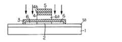
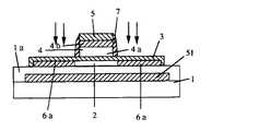
工程4(図4参照):前記多結晶シリコン膜2を薄膜トランジスタの能動層として用いるために、フォトリソグラフィ技術、RIE法によるドライエッチング技術により前記多結晶シリコン膜2を所定形状に加工する。 Step 4 (see FIG. 4): In order to use the
そして、前記多結晶シリコン膜2の上に、ロードロック式減圧CVD装置を用いた減圧CVD法により、ゲート絶縁膜としてのLTO膜(Low Temperature Oxide:シリコン酸化膜)3(膜厚1000Å)を形成する。 Then, an LTO film (Low Temperature Oxide: silicon oxide film) 3 (thickness 1000 mm) as a gate insulating film is formed on the
工程5(図5参照):前記ゲート絶縁膜3の上に、減圧CVD法により非晶質シリコン膜(膜厚2000Å)4aを堆積する。この非晶質シリコン膜4aは、その形成時に不純物(N型ならヒ素やリン、P型ならボロン)がドープされているが、ノンドープ状態で堆積し、その後に不純物を注入してもよい。 Step 5 (see FIG. 5): An amorphous silicon film (film thickness: 2000 mm) 4a is deposited on the
次に、スパッタ法を用い、前記非晶質シリコン膜4aの上にタングステンシリサイド(WSiX)膜4b(膜厚1000Å)を形成する。スパッタ法では、Wシリサイドの合金ターゲットを使用する。Wシリサイド(WSiX)の化学量論的組成はX=2であるが、合金ターゲットの組成はX>2に設定する。これはWシリサイド膜4bの組成がX=2に近いと、その後の熱処理時に非常に大きな引っ張り応力が生じ、Wシリサイド膜4bにクラックが発生したり、剥離したりする恐れがあるためである。但し、Wシリサイドの抵抗値はX=2の場合に最も低くなるため、クラックや剥離が生じない程度にXの上限を設定する必要がある。Next, a tungsten silicide (WSix )
そして、常圧CVD法により、前記Wシリサイド膜4bの上にシリコン酸化膜5を堆積した後、フォトリソグラフィ技術、RIE法によるドライエッチング技術を用いて、前記多結晶シリコン膜4a、Wシリサイド膜4b及びシリコン酸化膜5を所定形状に加工する。前記非晶質シリコン膜4aは、前記Wシリサイド膜4bとともにポリサイド構造のゲート電極4として使用する。 Then, after depositing a
工程6(図6参照):自己整合技術により、ゲート電極4及びシリコン酸化膜5をマスクとして、多結晶シリコン膜2に不純物を注入し、ソース/ドレイン領域6を形成する。 Step 6 (see FIG. 6): Impurities are implanted into the
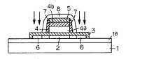
工程7(図7参照):前記ゲート絶縁膜3及びシリコン酸化膜5の上に、常圧CVD法によりシリコン酸化膜を堆積し、これを異方性全面エッチバックすることにより、前記ゲート電極4及びシリコン酸化膜5の側方にサイドウォール7を形成する。更に、このサイドウォール7及びシリコン酸化膜5をレジスト8で覆い、再び自己整合技術により、レジスト8をマスクとして多結晶シリコン膜2に不純物を注入して、LDD(Lightly Doped Drain)構造を形成する。 Step 7 (see FIG. 7): A silicon oxide film is deposited on the
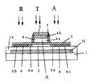
工程8(図8参照):この状態で、RTA(Rapid Thermal Annealing)法による急速加熱を行う。 Step 8 (see FIG. 8): In this state, rapid heating is performed by an RTA (Rapid Thermal Annealing) method.
即ち、図30において、105はシート状のアニール光を発する光源であり、キセノン(Xe)アークランプ106とそれを包む反射鏡107を1組として、これを上下に相対向させることにより構成している。108、108は基板1を搬送するためのローラー、109は予熱用のプリヒーター、110は加熱後の基板が急激に冷却されてひび割れしないようにするための補助ヒーターである。 That is, in FIG. 30,
このような構成において、基板1をプリヒーター106で予熱した後、シート状のアニール光源105を通して、熱処理する。 In such a configuration, the
この時のRTAの条件は、熱源:Xeアークランプ、温度:700〜950℃(パイロメータ)、雰囲気:N2、時間:1〜3秒である。RTA法による加熱は、高温を用いるが、きわめて短時間で終えることができるので、基板1が変形する心配はない。The RTA conditions at this time are: heat source: Xe arc lamp, temperature: 700 to 950 ° C. (pyrometer), atmosphere: N2 , time: 1 to 3 seconds. Although heating by the RTA method uses a high temperature, since it can be completed in a very short time, there is no fear that the
尚、基板1に対し、急激に高い温度を加えることが心配な場合は、RTAを複数回に分けて行ってもよい。即ち、各回の時間は1〜3秒とし、回を重ねる毎に温度を、初回:400℃〜最終回:700〜950℃というように段階的に上昇させる。 In addition, when it is anxious about applying high temperature with respect to the board |
前記Xeアークランプの光熱は、多結晶部よりも非晶質部やシリサイド部に強く吸収されるため、必要な部分のみを重点的に加熱することが可能になり、(ゲート)配線の低抵抗化や不純物の活性化に適している。 Since the photoheat of the Xe arc lamp is absorbed more strongly in the amorphous part and the silicide part than in the polycrystalline part, it becomes possible to heat only the necessary part, and the low resistance of the (gate) wiring. Suitable for activation and impurity activation.
そして、この急速加熱により、前記ソース/ドレイン領域6の不純物が活性化するとともに前記非晶質シリコン膜4aが多結晶化され、更には、この多結晶シリコン膜4aとWシリサイド膜4bとによるポリサイド構造のゲート電極4のシート抵抗が、約20〜22Ω/□にまで下がる。 The rapid heating activates the impurities in the source /
また、活性化処理を行ったソース/ドレイン領域6のシート抵抗も、n型で1〜1.5kΩ/□、p型で1〜1.2kΩ/□と、高温プロセスで用いられる拡散炉による高温熱処理と同等のものとなる。 Further, the sheet resistance of the source /
この工程により、薄膜トランジスタ(TFT:Thin Film Transistor)Aが形成される。 Through this process, a thin film transistor (TFT) A is formed.
工程9(図9参照):レジスト8除去後、デバイスの全面に、プラズマ酸化膜(膜厚2000Å)と常圧CVD法によるシリコン酸化膜(膜厚2000Å)との積層構造から成る層間絶縁膜9を形成する。層間絶縁膜9を常圧CVD法によるシリコン酸化膜だけで形成すると、堆積膜厚が不均一になって、オーバーハングが形成され、後工程で使用するAlなどが除去されずに残りやすく、絶縁不良が発生する危惧がある。一方、本実施形態のように、プラズマ酸化膜を堆積した後に常圧でシリコン酸化膜を堆積する方法にあっては、シリコン酸化膜の成長レートが安定し、その堆積膜厚が均一になる。 Step 9 (see FIG. 9): After the resist 8 is removed, an
特に、プラズマ酸化膜は、基板表面の凹凸に合わせて均一な膜厚で堆積されるので、層間絶縁膜としての総膜厚が均一に安定する。 In particular, since the plasma oxide film is deposited with a uniform film thickness according to the unevenness of the substrate surface, the total film thickness as the interlayer insulating film is stabilized uniformly.
プラズマ酸化膜の堆積条件は、堆積温度:390℃、RF出力:500W、SiH4流量:500sccm、酸素流量:1500sccm、圧力:9torrとし、シリコン酸化膜の堆積条件は、堆積温度:400℃、キャリアN2ガス流量:3000ccとする。The deposition conditions of the plasma oxide film are deposition temperature: 390 ° C., RF output: 500 W, SiH4 flow rate: 500 sccm, oxygen flow rate: 1500 sccm, pressure: 9 torr. The deposition conditions of the silicon oxide film are deposition temperature: 400 ° C., carrier. N2 gas flow rate: 3000 cc.
続いて、電気炉により、水素(H2)雰囲気中、温度450℃で12時間加熱し、更に、水素プラズマ処理を施す。このような水素化処理を行うことで、多結晶シリコン膜の結晶欠陥部分に水素原子が結合し、結晶構造が安定化して、電界効果移動度が高まる。Subsequently, it is heated in a hydrogen (H2 ) atmosphere at a temperature of 450 ° C. for 12 hours by an electric furnace, and further subjected to hydrogen plasma treatment. By performing such hydrogenation treatment, hydrogen atoms are bonded to the crystal defect portion of the polycrystalline silicon film, the crystal structure is stabilized, and the field effect mobility is increased.
その後、フォトリソグラフィ技術、RIE法によるドライエッチング技術を用いて、前記層間絶縁膜9に、前記ソース・ドレイン領域6とコンタクトするコンタクトホール10を形成する。 Thereafter, contact holes 10 that are in contact with the source /
工程10(図10参照):マグネトロンスパッタ法により、Ti/Al−Si合金/Tiの積層構造からなる配線層を堆積し、フォトリソグラフィ技術、RIE法によるドライエッチング技術を用いて、ソース・ドレイン電極11として加工する。 Step 10 (see FIG. 10): A wiring layer having a laminated structure of Ti / Al—Si alloy / Ti is deposited by magnetron sputtering, and a source / drain electrode is formed by using a photolithography technique and a dry etching technique by RIE. 11 is processed.
工程11(図11参照):CVD法により、デバイスの全面に保護膜としてのシリコン酸化膜12(シリコン窒化膜でもよい)を薄く堆積させる。 Step 11 (see FIG. 11): A silicon oxide film 12 (or a silicon nitride film) as a protective film is thinly deposited on the entire surface of the device by CVD.
工程12(図12参照):デバイス全面に、SOG(Spin On Glass)膜13を3回にわたって塗布し、デバイス表面の凹凸を平坦化する。 Step 12 (see FIG. 12): An SOG (Spin On Glass)
工程13(図13参照):前記SOG膜13はレジストの剥離性が悪く、また水分を吸収しやすいので、この保護膜として、CVD法により、SOG膜13の上に更にシリコン酸化膜14(シリコン窒化膜でもよい)を薄く堆積させる。 Step 13 (see FIG. 13): Since the
工程14(図14参照):フォトリソグラフィ技術、RIE法によるドライエッチング技術を用いて、前記シリコン酸化膜12/SOG膜13/シリコン酸化膜14に、前記ソース・ドレイン電極11に通じるコンタクトホール15を形成し、デバイスの全面に、画素電極としてのITO膜16をスパッタ蒸着させる。 Step 14 (see FIG. 14): Contact holes 15 communicating with the source /
工程15(図15参照):最後に、ITO膜16を電極形状に加工すべく、ITO膜16の上にレジストパターンを形成した後、まず、臭化水素ガス(HBr)を用いたRIE法によりITO膜16をエッチングし、シリコン酸化膜14が露出しはじめた時点で、ガスを塩素ガス(Cl2)に切り替え、そのまま最後までエッチングを継続する。Step 15 (see FIG. 15): Finally, a resist pattern is formed on the
工程16(図16参照):このようにLCDの片側TFT基板を形成した後は、表面に共通電極17が形成された透明絶縁基板18を相対向させ、各基板1、18の間に液晶を封入して液晶層19を形成することにより、LCDの画素部を完成させる。 Step 16 (see FIG. 16): After forming the one-side TFT substrate of the LCD in this way, the transparent insulating
図17は本実施形態におけるアクティブマトリクス方式LCDのブロック構成図である。 FIG. 17 is a block diagram of an active matrix LCD according to this embodiment.
画素部20には各走査線(ゲート配線)G1・・・Gn,Gn+1・・・Gmと各データ線(ドレイン配線)D1・・・Dn,Dn+1・・・Dmとが配置されている。各ゲート配線と各ドレイン配線とはそれぞれ直交し、その直交部分に画素21が設けられている。そして、各ゲート配線は、ゲートドライバ22に接続され、ゲート信号(走査信号)が印加されるようになっている。また、各ドレイン配線は、ドレインドライバ(データドライバ)23に接続され、データ信号(ビデオ信号)が印加されるようになっている。これらのドライバ22、23によって周辺駆動回路24が構成されている。 Each scanning line (gate wiring) G1... Gn, Gn + 1... Gm and each data line (drain wiring) D1... Dn, Dn + 1. ing. Each gate line and each drain line are orthogonal to each other, and a
そして、各ドライバ22、23のうち少なくともいずれか一方を画素部20と同一基板上に形成したLCDは、一般にドライバ一体型(ドライバ内蔵型)LCDと呼ばれている。尚、ゲートドライバ22が、画素部20の両端に設けられている場合もある。また、ドレインドライバ23が、画素部20の両側に設けられている場合もある。 An LCD in which at least one of the
この周辺駆動回路24のスイッチング用素子にも前記多結晶シリコンTFT(A)と同等の製造方法で作成した多結晶シリコンTFTを用いており、多結晶シリコンTFT(A)の作製に並行して、同一基板上に形成される。尚、この周辺駆動回路24用の多結晶シリコンTFTは、LDD構造ではなく、通常のシングルドレイン構造を採用している(もちろん、LDD構造であってもよい)。 The switching element of the
また、この周辺駆動回路24の多結晶シリコンTFTは、CMOS構造に形成することにより、各ドライバ22、23としての寸法の縮小化を実現している。図18にゲート配線Gnとドレイン配線Dnとの直交部分に設けられている画素21の等価回路を示す。 In addition, the polycrystalline silicon TFT of the
画素21は、画素駆動素子としてのTFT(前記薄膜トランジスタAと同様)、液晶セルLC、補助容量Csから構成される。ゲート配線GnにはTFTのゲートが接続され、ドレイン配線DnにはTFTのドレインが接続されている。そして、TFTのソースには、液晶セルLCの表示電極(画素電極)と補助容量(蓄積容量又は付加容量)Csとが接続されている。 The
この液晶セルLCと補助容量Csとにより、信号蓄積素子が構成される。液晶セルLCの共通電極(表示電極の反対側の電極)には電圧Vcomが印加されている。一方、補助容量Csにおいて、TFTのソースと接続される側の反対側の電極には定電圧VRが印加されている。この液晶セルLCの共通電極は、文字通り全ての画素21に対して共通した電極となっている。そして、液晶セルLCの表示電極と共通電極との間には静電容量が形成されている。尚、補助容量Csにおいて、TFTのソースと接続される側の反対側の電極は、隣のゲート配線Gn+1と接続されている場合もある。 The liquid crystal cell LC and the auxiliary capacitor Cs constitute a signal storage element. A voltage Vcom is applied to the common electrode (electrode opposite to the display electrode) of the liquid crystal cell LC. On the other hand, in the auxiliary capacitor Cs, a constant voltage VR is applied to the electrode opposite to the side connected to the TFT source. The common electrode of the liquid crystal cell LC is literally a common electrode for all the
このように構成された画素21において、ゲート配線Gnを正電圧にしてTFTのゲートに正電圧を印加すると、TFTがオンとなる。すると、ドレイン配線Dnに印加されたデータ信号で、液晶セルLCの静電容量と補助容量Csとが充電される。反対に、ゲート配線Gnを負電圧にしてTFTのゲートに負電圧を印加すると、TFTがオフとなり、その時点でドレイン配線Dnに印加されていた電圧が、液晶セルLCの静電容量と補助容量Csとによって保持される。このように、画素21へ書き込みたいデータ信号をドレイン配線に与えてゲート配線の電圧を制御することにより、画素21に任意のデータ信号を保持させておくことができる。その画素21の保持しているデータ信号に応じて液晶セルLCの透過率が変化し、画像が表示される。 In the
ここで、画素21の特性として重要なものに、書き込み特性と保持特性とがある。書き込み特性に対して要求されるのは、画素部20の仕様から定められた単位時間内に、信号蓄積素子(液晶セルLC及び補助容量Cs)に対して所望のビデオ信号電圧を十分に書き込むことができるかどうかという点である。また、保持特性に対して要求されるのは、信号蓄積素子に一旦書き込んだビデオ信号電圧を必要な時間だけ保持することができるかどうかという点である。 Here, the important characteristics of the
補助容量Csが設けられているのは、信号蓄積素子の静電容量を増大させて書き込み特性及び保持特性を向上させるためである。すなわち、液晶セルLCは、その構造上、静電容量の増大には限界がある。そこで、補助容量Csによって液晶セルLCの静電容量の不足分を補うわけである。
(第2実施形態)
次に、本発明を具体化した第2の実施形態を図19〜図28に基づいて説明する。但し、第1実施形態で説明した個所と同等の個所には同じ符号を用い説明を省略する。また、この第2実施形態は、第1実施形態の工程1〜工程8に対応する工程が異なるので、ここではその部分のみを説明する。The auxiliary capacitor Cs is provided in order to increase the capacitance of the signal storage element and improve the writing characteristics and the holding characteristics. That is, the liquid crystal cell LC has a limit in increasing the capacitance because of its structure. Therefore, the auxiliary capacitance Cs compensates for the shortage of the capacitance of the liquid crystal cell LC.
(Second Embodiment)
Next, a second embodiment embodying the present invention will be described with reference to FIGS. However, the same reference numerals are used for portions equivalent to those described in the first embodiment, and description thereof is omitted. Moreover, since this 2nd Embodiment differs in the process corresponding to the process 1-the
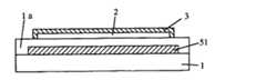
工程(1)(図19参照):基板1上に、Wシリサイド膜51を形成する。 Step (1) (see FIG. 19):
工程(2)(図20参照):前記Wシリサイド膜51を、トランジスタの能動層としての多結晶シリコンと同じパターンに加工する。 Step (2) (see FIG. 20): The
工程(3)(図21参照):前記基板1及びWシリサイド膜51を覆うように、SiO2やSiNなどの絶縁性薄膜1aをCVD法やスパッタ法などにより形成する。Step (3) (see FIG. 21): An insulating
工程(4)(図22参照):前記絶縁性薄膜1aの上に、非晶質シリコン膜2aを形成する。 Step (4) (see FIG. 22): An
工程(5)(図23参照):前記非晶質シリコン膜2aの表面にKrFエキシマレーザービームを走査してアニール処理を行い、非晶質シリコン膜2aを溶融再結晶化して、多結晶シリコン薄膜2を形成する。 Step (5) (see FIG. 23): The surface of the
尚、レーザービームとして、XeClエキシマレーザーやArFエキシマレーザーを使用してもよい。 A XeCl excimer laser or an ArF excimer laser may be used as the laser beam.
工程(6)(図24参照):前記多結晶シリコン膜2を薄膜トランジスタの能動層として用いるために、フォトリソグラフィ技術、RIE法によるドライエッチング技術により前記多結晶シリコン膜2を所定形状に加工する。 Step (6) (see FIG. 24): In order to use the
そして、前記多結晶シリコン膜2の上に、ゲート絶縁膜としてのLTO膜3を形成する。 Then, an
工程(7)(図25参照):前記ゲート絶縁膜3の上に、非晶質シリコン膜4aを堆積する。 Step (7) (see FIG. 25): An
次に、前記非晶質シリコン膜4aの上にWシリサイド膜4bを形成する。 Next, a
そして、前記Wシリサイド膜4bの上にシリコン酸化膜5を堆積した後、フォトリソグラフィ技術、RIE法によるドライエッチング技術を用いて、前記多結晶シリコン膜4a、Wシリサイド膜4b及びシリコン酸化膜5を所定形状に加工する。前記非晶質シリコン膜4aは、前記Wシリサイド膜4bとともにポリサイド構造のゲート電極4として使用する。 Then, after depositing a
工程(8)(図26参照):前記ゲート絶縁膜3及びシリコン酸化膜5の上に、常圧CVD法によりシリコン酸化膜を堆積し、これを異方性全面エッチバックすることにより、前記ゲート電極4及びシリコン酸化膜5の側方にサイドウォール7を形成する。 Step (8) (see FIG. 26): A silicon oxide film is deposited on the
そして、自己整合技術により、サイドウォール7をマスクとして、多結晶シリコン膜2に、加速電圧:80KeV、ドーズ量3×1013cm-2の条件で、リン(P)イオンを不純物として注入し、低濃度の不純物領域6aを形成する。Then, by the self-alignment technique, phosphorus (P) ions are implanted as impurities into the
工程(9)(図27参照):前記サイドウォール7及びシリコン酸化膜5をレジスト8で覆い、再び自己整合技術により、レジスト8をマスクとして多結晶シリコン膜2に、加速電圧:80KeV、ドーズ量1×1015cm-2の条件で、リン(P)イオンを不純物として注入し、高濃度の不純物領域6bを形成することにより、LDD(Lightly Doped Drain)構造のソース/ドレイン領域6を形成する。Step (9) (see FIG. 27): The
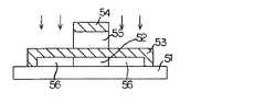
工程(10)(図28参照):この状態で、第1実施形態と同様のRTA法による急速加熱を行う。 Step (10) (see FIG. 28): In this state, rapid heating is performed by the RTA method similar to that of the first embodiment.
Xeアークランプの光熱は、多結晶部よりも非晶質部やシリサイド部に強く吸収されるため、必要な部分のみを重点的に加熱することが可能になり、(ゲート)配線の低抵抗化や不純物の活性化に適している。 Xe arc lamp photothermal energy is absorbed more strongly in the amorphous part and silicide part than in the polycrystalline part, so that only the necessary part can be heated preferentially, and the resistance of the (gate) wiring is reduced. Suitable for activation of impurities.
特に、本実施形態では、多結晶シリコン膜2に対応して、その下方にWシリサイド膜51を形成している。このWシリサイド膜51は、RTAの熱を吸収する作用があり、熱を吸収したWシリサイド膜51からの放射熱によっても前記多結晶シリコン膜2の不純物の活性化が行われる。 In particular, in the present embodiment, the
即ち、多結晶シリコン膜2を、Xeアークランプによる熱とWシリサイド膜51からの放射熱とにより、直接及び間接的に加熱することにより、多結晶シリコン膜2全体を均一に加熱し、活性化がバラツクことなく良好に行われるようにする。 That is, the
Wシリサイド膜51の大きさは、基本的に、多結晶シリコン膜2と同じか又はそれ以上であればよいが、面内でのパターンの大きさに対応した面積となるように調整すれば、なお好ましい。 The size of the
即ち、集積化半導体デバイスでは、パターンの疎密が基板上に発生するため、各トランジスタに均等にWシリサイド膜2を設けたのでは、場所によって単位面積当りの熱吸収率が異なり、均一な熱処理が行えず、また、Wシリサイド膜51が集中する場所での温度が非常に高くなって基板1が変形する場合がある。 That is, in an integrated semiconductor device, pattern density occurs on the substrate. Therefore, if the
そこで、下層に配置した熱吸収膜の単位面積当りの密度を、その上層に形成されるパターンに係わらずほぼ一定となるようにすれば、RTAで活性化するときの温度分布の偏りを解消することができる。具体的にドライバー一体型のLCDパネルでは、ドライバ部に比べて画素部のトランジスタの密度が高いので、ドライバ部のトランジスタに対応するWシリサイド膜51の大きさを、画素部のそれに比べて大きくしてやることで、基板1全体の温度分布がほぼ均一になる。 Therefore, if the density per unit area of the heat absorption film disposed in the lower layer is made substantially constant regardless of the pattern formed in the upper layer, the temperature distribution bias when activated by RTA is eliminated. be able to. Specifically, in the driver-integrated LCD panel, the density of the transistors in the pixel portion is higher than that in the driver portion. Therefore, the size of the
LCDパネルにあっては、回路の面積の約10%がWシリサイド膜51となるように調整することが好ましい。 In the LCD panel, it is preferable to adjust so that about 10% of the circuit area becomes the
この工程により、多結晶シリコンTFT(TFT:Thin Film Transistor)(A)が形成される。 By this step, a polycrystalline silicon TFT (TFT: Thin Film Transistor) (A) is formed.
以上の実施形態により製造した多結晶シリコンTFTにあっては、いわゆる低温プロセスで行うことができ、しかも、良質の多結晶シリコン膜を能動層として使用している。 The polycrystalline silicon TFT manufactured by the above embodiment can be performed by a so-called low temperature process, and a high-quality polycrystalline silicon film is used as an active layer.
本発明者の実験によれば、nチャネルのMOS型多結晶シリコンTFTでの移動度μnが200cm2/V・S以上、pチャネルのMOS型多結晶シリコンTFTでの移動度μpが150cm2/V・S以上と、高い性能のトランジスタを実現できることが分かった。According to the experiments by the present inventors, the mobility μn in the n-channel MOS type polycrystalline silicon TFT is 200 cm2 / V · S or more, and the mobility μp in the p-channel MOS type polycrystalline silicon TFT is 150 cm2 / V. It was found that a transistor with high performance of V · S or higher can be realized.
このような高性能TFTにあっては、例えば、μn=50cm2/V・S、μp=20cm2/V・Sが要求されるNTSCテレビ信号表示用LCDパネルにも十分に適用可能であり、μn=50cm2/V・S、μp=20cm2/V・S、しきい値電圧:2V(nチャネル)、−5V(pチャネル)、S値(Sub-threshold swing):0.2V/decade、オン・オフ比:1×107の特性を得ることができる。Such a high-performance TFT is sufficiently applicable to, for example, an LCD panel for NTSC television signal display that requires μn = 50 cm2 / V · S and μp = 20 cm2 / V · S, μn = 50 cm2 / V · S, μp = 20 cm2 / V · S, threshold voltage: 2 V (n channel), −5 V (p channel), S value (Sub-threshold swing): 0.2 V / decade The on / off ratio of 1 × 10⁷ can be obtained.
また、移動度が高いぶん、TFTの駆動能力が向上するので、TFTのサイズを小さくすることができ、従来能動層として非晶質シリコンを用いたトランジスタのサイズ(W/L=34/10μm)に比べて、1/8以下のサイズ(W/L=8/5μm)に縮小することができる。更には、高品質の能動層であるので、トランジスタOFF時のリーク電流も少なく、そのぶん補助容量の面積も1/3以下に縮小することができる。 Also, the higher the mobility, the better the driving capability of the TFT, so that the size of the TFT can be reduced, and the size of a transistor that conventionally uses amorphous silicon as the active layer (W / L = 34/10 μm). Can be reduced to a size of 1/8 or less (W / L = 8/5 μm). Furthermore, since it is a high quality active layer, there is little leakage current when the transistor is OFF, and the area of the auxiliary capacitor can be reduced to 1/3 or less.
具体的には、サイズ2.4型で、画素ピッチ:50.0(H)μm×1500(V)μm、画素数:23万ドット(320×3(RGB)×240)と、従来型のパネルに比べて3倍以上の高密度画素を有しながらも、55%という高開口率(従来比:1.5倍)のものを得ることができ、高輝度化を実現できる。 Specifically, the size is 2.4 type, pixel pitch: 50.0 (H) μm × 1500 (V) μm, number of pixels: 230,000 dots (320 × 3 (RGB) × 240), While having a
以上の実施形態は以下のように変更してもよく、その場合でも同様の作用、効果を得ることができる。 The above embodiment may be modified as follows, and even in that case, the same operation and effect can be obtained.
(1)条件にもよるが基板1として、通常のガラス板なども使用可能である。 (1) Depending on the conditions, a normal glass plate or the like can be used as the
(2)工程2や工程(4)において、非晶質シリコン膜を減圧CVD法により、例えば、モノシランガスを用い、温度580℃で堆積させる。これにより、非晶質シリコン膜2aは微結晶を含んだ膜となる。 (2) In
微結晶を含んだ非晶質シリコン膜を固相成長法により多結晶化することにより、結晶粒径が小さくなるぶん移動度は若干低下するが、結晶成長を短時間で終えることができる。 When an amorphous silicon film containing microcrystals is polycrystallized by a solid phase growth method, the crystal grain size is reduced, but the mobility is slightly reduced, but the crystal growth can be completed in a short time.
(3)工程2や工程(4)において、非晶質シリコン膜2aを減圧CVD法、プラズマCVD法によらず、常圧CVD法、光励起CVD法、蒸着法、EB(Electron Beam)蒸着法、MBE(Molecular Beam Epitaxy)法、スパッタ法からなるグループの内のいずれか一つの方法によって形成する。 (3) In the
(4)多結晶シリコン膜2のチャネル領域に相当する部分に不純物をドーピングして多結晶シリコンTFTのしきい値電圧(Vth)を制御する。固相成長法で形成した多結晶シリコンTFTにおいては、Nチャネルトランジスタではディプレッション方向にしきい値電圧がシフトし、Pチャネルトランジスタではエンハンスメント方向にしきい値電圧がシフトする傾向にある。また、水素化処理を行った場合には、その傾向がより顕著となる。このしきい値電圧のシフトを抑えるには、チャネル領域に不純物をドーピングすればよい。 (4) Impurities are doped into the portion corresponding to the channel region of the
(5)工程5、工程(1)、工程(7)において、スパッタ法以外のPVD方法(真空蒸着法、イオンプレーティング法、イオンビームデポジション法、クラスターイオンビーム法など)を用いて、Wシリサイド膜4b、51を形成する。この場合にも、前記したスパッタ法の場合と同様な理由により、Wシリサイド(WSiX)の組成をX>2に設定する。(5) In
(6)工程5、工程(1)、工程(7)において、CVD法を用いてWシリサイド膜4b、51を形成する。そのソースガスとしては、六フッ化タングステン(WF6)とシラン(SiH4)を用いればよい。成膜温度は、350〜450℃前後とする。この場合にも、前記したスパッタ法の場合と同様な理由により、Wシリサイド(WSiX)の組成をX>2に設定する。CVD法はPVD法に比べ、段差被覆性が優れているため、Wシリサイド膜4bの膜厚をより均一にすることができる。(6) In
(7)ゲート電極に用いるWシリサイドに代わるものとして、MoSi2、TiSi2、TaSi2、CoSi2などの高融点金属シリサイド、その他、W、Mo、Co、Cr、Ti、Taなどの高融点金属を用いてもよい。(7) As an alternative to W silicide used for the gate electrode, refractory metal silicides such as MoSi2 , TiSi2 , TaSi2 , CoSi2 , and other refractory metals such as W, Mo, Co, Cr, Ti, Ta May be used.
(8)工程9において、プラズマ酸化膜に代えて、TEOS(Tetra Ethyl Ortho Silicate又はTetra-ethoxy-silane)を用いたプラズマTEOS酸化膜を用いてもよく、また、シリコン酸化膜に代えて、常圧オゾンTEOS酸化膜を用いてもよい。 (8) In
プラズマTEOS酸化膜の堆積条件は、堆積温度:390℃、RF出力:500W、TEOS流量:500sccm、酸素流量:600sccm、圧力:9torrとし、常圧オゾンTEOS酸化膜の堆積条件は、堆積温度:400℃、RF出力:オゾン濃度:約5wt%、TEOSキャリアN2ガス流量:3000ccとする。The deposition conditions for the plasma TEOS oxide film are deposition temperature: 390 ° C., RF output: 500 W, TEOS flow rate: 500 sccm, oxygen flow rate: 600 sccm, pressure: 9 torr, and the deposition conditions for atmospheric pressure ozone TEOS oxide film are deposition temperature: 400 ° C, RF output: ozone concentration: about 5 wt%, TEOS carrier N2 gas flow rate: 3000 cc.
(9)上記(8)の工程の後、プラズマTEOS酸化膜を、アンモニア(NH3)ガスを用いてプラズマ処理することにより窒素イオンに晒し、その表面を窒化してから常圧オゾンTEOS酸化膜を堆積すると、シリコン酸化膜の成長レートがより安定する。この時の窒化処理条件は、温度:360℃、RF出力:500W、アンモニア流量:100〜500sccm、N2流量:0〜400sccmである。尚、この窒化処理において、アンモニアの代わりに窒素を用いてもよい。(9) After the step (8), the plasma TEOS oxide film is exposed to nitrogen ions by plasma treatment using ammonia (NH3 ) gas, the surface is nitrided, and then the atmospheric pressure ozone TEOS oxide film As a result, the growth rate of the silicon oxide film becomes more stable. The nitriding conditions at this time are as follows: temperature: 360 ° C., RF output: 500 W, ammonia flow rate: 100 to 500 sccm, N2 flow rate: 0 to 400 sccm. In this nitriding treatment, nitrogen may be used instead of ammonia.
(10)Wシリサイド膜51に代えて、非結晶質シリコン膜や多結晶シリコン膜などの半導体膜を用いる。これらのシリコン膜には不純物がドープされていてもよい。このように、導電性膜又は半導体膜を用いることにより、この熱吸収膜に電圧を印加することで、TFTを、LSIに用いられるMOSトランジスタのように4端子デバイスとして動作させて、しきい値電圧をコントロールできると共に、ガラス基板を用いた場合には、基板内のイオンを静電的にシールドするため、ガラス基板内のイオンによるトランジスタの特性劣化及び可動イオンが形成する電位によるTFTへの悪影響を防止することができる。 (10) Instead of the
(11)Wシリサイド膜51に代えて、MoSi2、TiSi2、TaSi2、CoSi2などの高融点金属シリサイド、その他、W、Mo、Co、Cr、Ti、Taなどの高融点金属を用いてもよい。更には、使用温度が低い場合には(約450℃以下)、AlやAuなどのいわゆる低融点金属を用いてもよい。(11) Instead of the
Wシリサイド膜も含めて、これらの金属膜は、光を通さない性質を有しているので、以下の通りの効果を有する。 These metal films, including the W silicide film, have the following effects because they have the property of not allowing light to pass through.
(a)光の散乱を防止すると共に液晶セルに斜めから入ろうとする不要な光を遮るので、LCDデバイスとしてコントラストが高くなる。 (A) Since the light scattering is prevented and unnecessary light entering the liquid crystal cell from an oblique direction is blocked, the contrast of the LCD device is increased.
(b)TFTに入ろうとする光を遮るので、光によるリーク電流を減少させてTFTとしての特性を向上させると共に光によるTFT自身の劣化を防止する。 (B) Since the light entering the TFT is blocked, the leakage current due to the light is reduced to improve the characteristics as the TFT and the deterioration of the TFT itself due to the light is prevented.
(12)プレーナ型だけでなく、逆プレーナ型、スタガ型、逆スタガ型などあらゆる構造の多結晶シリコンTFTに適用する。 (12) The present invention is applied not only to a planar type but also to a polycrystalline silicon TFT having any structure such as an inverted planar type, a staggered type, and an inverted staggered type.
(13)多結晶シリコンTFTだけでなく、絶縁ゲート型半導体素子全般に適用する。また、太陽電池や光センサなどの光電変換素子、バイポーラトランジスタ、静電誘導型トランジスタ(SIT:Static Induction Transistor)などの多結晶シリコン膜を用いるあらゆる半導体装置に適用する。 (13) Applicable not only to polycrystalline silicon TFTs but also to insulated gate semiconductor devices in general. Further, the present invention is applied to any semiconductor device using a polycrystalline silicon film such as a photoelectric conversion element such as a solar cell or an optical sensor, a bipolar transistor, or a static induction transistor (SIT).
1 絶縁基板
2a 非晶質シリコン膜
2 多結晶シリコン膜
3 ゲート絶縁膜
4a 多結晶シリコン膜(非晶質シリコン膜)
4b Wシリサイド膜
4 ゲート電極
6 不純物領域DESCRIPTION OF
4b
Claims (9)
Translated fromJapanese前記非晶質シリコン膜をレーザーアニールして多結晶シリコン膜を形成する第2の工程と、
前記多結晶シリコン膜に、ソース/ドレイン領域としての不純物領域を形成する第3の工程と、
前記不純物領域を、シート状のアニール光を発する光源を有するRTA(Rapid Thermal Annealing)法を用いて急速加熱することにより活性化する第4の工程と、を備え、
前記光源が、ランプと前記ランプを覆う反射鏡とから構成されていることを特徴とした半導体装置の製造方法。A first step of forming an amorphous silicon film on a substrate;
A second step of forming a polycrystalline silicon film by laser annealing the amorphous silicon film;
A third step of forming impurity regions as source / drain regions in the polycrystalline silicon film;
A fourth step of activating the impurity region by rapid heating using an RTA (Rapid Thermal Annealing) method having a light source that emits sheet-like annealing light,
The method of manufacturing a semiconductor device, wherein the light source is composed of a lamp and a reflecting mirror covering the lamp.
前記非晶質シリコン膜をレーザーアニールして多結晶シリコン膜を形成する第2の工程と、
前記多結晶シリコン膜に、ソース/ドレイン領域としての不純物領域を形成する第3の工程と、
前記不純物領域を、シート状のアニール光を発する光源を有するRTA(Rapid Thermal Annealing)法を用いて急速加熱することにより活性化する第4の工程と、を備え、
前記光源が、ランプと前記ランプからの光を反射する反射鏡とから構成されていることを特徴とした半導体装置の製造方法。A first step of forming an amorphous silicon film on a substrate;
A second step of forming a polycrystalline silicon film by laser annealing the amorphous silicon film;
A third step of forming impurity regions as source / drain regions in the polycrystalline silicon film;
A fourth step of activating the impurity region by rapid heating using an RTA (Rapid Thermal Annealing) method having a light source that emits sheet-like annealing light,
A method of manufacturing a semiconductor device, wherein the light source includes a lamp and a reflecting mirror that reflects light from the lamp.
シート状に加工されたレーザービームを前記非晶質シリコン膜に照射することにより前記非晶質シリコン膜をアニールして多結晶シリコン膜を形成する第2の工程と、
前記多結晶シリコン膜に、ソース/ドレイン領域としての不純物領域を形成する第3の工程と、
前記不純物領域を、ランプを熱源として急速加熱することにより活性化する第4の工程と、を含み、
前記第4の工程は、前記基板を予熱する工程と、一対のランプを相対向させた状態で、この一対のランプ間に前記基板を搬送する工程と、を含むことを特徴とした半導体装置の製造方法。A first step of forming an amorphous silicon film on a substrate;
A second step of annealing the amorphous silicon film by irradiating the amorphous silicon film with a laser beam processed into a sheet shape to form a polycrystalline silicon film;
A third step of forming impurity regions as source / drain regions in the polycrystalline silicon film;
A fourth step of activating the impurity region by rapid heating using a lamp as a heat source,
The fourth step includes a step of preheating the substrate, and a step of transporting the substrate between the pair of lamps in a state where the pair of lamps are opposed to each other. Production method.
前記非晶質シリコン膜をレーザーアニールして多結晶シリコン膜を形成する第2の工程と、
前記多結晶シリコン膜に、不純物領域を形成する第3の工程と、
前記不純物領域を、ランプを熱源として急速加熱することにより活性化する第4の工程と、を含み、
前記第2の工程は、シート状に加工されたレーザービームを前記非晶質シリコン膜に照射することにより行い、
前記第4の工程は、前記基板を予熱する工程と、RTA(Rapid Thermal Annealing)法を用いて急速加熱する工程と、を含み、
前記RTA法を用いて急速加熱する工程は、シート状のアニール光を発するランプ光源を用い、かつ、前記ランプとして、キセノンアークランプを用いることを特徴とした半導体装置の製造方法。A first step of forming an amorphous silicon film on a substrate;
A second step of forming a polycrystalline silicon film by laser annealing the amorphous silicon film;
A third step of forming an impurity region in the polycrystalline silicon film;
A fourth step of activating the impurity region by rapid heating using a lamp as a heat source,
The second step is performed by irradiating the amorphous silicon film with a laser beam processed into a sheet shape,
The fourth step includes a step of preheating the substrate and a step of rapid heating using an RTA (Rapid Thermal Annealing) method,
The method of manufacturing a semiconductor device, wherein the rapid heating step using the RTA method uses a lamp light source that emits sheet-like annealing light, and uses a xenon arc lamp as the lamp.
Priority Applications (1)
| Application Number | Priority Date | Filing Date | Title |
|---|---|---|---|
| JP2004242135AJP2005051252A (en) | 1995-07-03 | 2004-08-23 | Method for manufacturing semiconductor device |
Applications Claiming Priority (2)
| Application Number | Priority Date | Filing Date | Title |
|---|---|---|---|
| JP16751395 | 1995-07-03 | ||
| JP2004242135AJP2005051252A (en) | 1995-07-03 | 2004-08-23 | Method for manufacturing semiconductor device |
Related Parent Applications (1)
| Application Number | Title | Priority Date | Filing Date |
|---|---|---|---|
| JP11240191ADivisionJP2000082822A (en) | 1995-07-03 | 1999-08-26 | Manufacture of semiconductor device |
Publications (1)
| Publication Number | Publication Date |
|---|---|
| JP2005051252Atrue JP2005051252A (en) | 2005-02-24 |
Family
ID=34276912
Family Applications (1)
| Application Number | Title | Priority Date | Filing Date |
|---|---|---|---|
| JP2004242135APendingJP2005051252A (en) | 1995-07-03 | 2004-08-23 | Method for manufacturing semiconductor device |
Country Status (1)
| Country | Link |
|---|---|
| JP (1) | JP2005051252A (en) |
- 2004
- 2004-08-23JPJP2004242135Apatent/JP2005051252A/enactivePending
Similar Documents
| Publication | Publication Date | Title |
|---|---|---|
| KR100376905B1 (en) | A semiconductor device and a display, and a method for manufacturing thereof | |
| US6455360B1 (en) | Method for forming crystalline semiconductor layers, a method for fabricating thin film transistors, and a method for fabricating solar cells and active matrix liquid crystal devices | |
| US6017779A (en) | Fabrication method for a thin film semiconductor device, the thin film semiconductor device itself, liquid crystal display, and electronic device | |
| US6790714B2 (en) | Semiconductor device, display device and method of fabricating the same | |
| US6984552B2 (en) | Method for doping semiconductor layer, method for producing thin film semiconductor element and thin film semiconductor element | |
| JP3968484B2 (en) | Thin film transistor manufacturing method | |
| JP2002184710A (en) | Semiconductor layer doping method, thin film semiconductor device manufacturing method, and thin film semiconductor device | |
| US6537864B1 (en) | Method of fabricating a thin film transistor using electromagnetic wave heating of an amorphous semiconductor film | |
| US7052944B2 (en) | Thin-film transistor and method of manufacture thereof | |
| JP3096640B2 (en) | Semiconductor device and display device | |
| JP3071129B2 (en) | Method for manufacturing semiconductor device | |
| JP3840697B2 (en) | Manufacturing method of semiconductor device, manufacturing method of active matrix substrate, and manufacturing method of liquid crystal display device | |
| JPH0974201A (en) | Manufacture of thin film transistor, and liquid crystal display | |
| JP3311522B2 (en) | Method for manufacturing semiconductor device | |
| JP3108331B2 (en) | Method for manufacturing thin film transistor | |
| JP2007250944A (en) | Method and apparatus for depositing semiconductor thin film | |
| JPH0936376A (en) | Manufacture of thin-film semiconductor device | |
| JPH0845867A (en) | Semiconductor device manufacture and displaying device | |
| JPH0951099A (en) | Semiconductor device, manufacture thereof, display device and manufacture of the display device | |
| JP2005051252A (en) | Method for manufacturing semiconductor device | |
| JP2000082821A (en) | Manufacture of semiconductor device and liquid crystal display | |
| JP2000082822A (en) | Manufacture of semiconductor device | |
| US20070026588A1 (en) | Method of fabricating a thin film transistor | |
| JP2004134809A (en) | Manufacturing method of semiconductor device | |
| JP2000208416A (en) | Crystallizing method for semiconductor thin film and laser irradiation apparatus |
Legal Events
| Date | Code | Title | Description |
|---|---|---|---|
| RD01 | Notification of change of attorney | Free format text:JAPANESE INTERMEDIATE CODE: A7421 Effective date:20051227 | |
| A131 | Notification of reasons for refusal | Free format text:JAPANESE INTERMEDIATE CODE: A131 Effective date:20080527 | |
| A521 | Written amendment | Free format text:JAPANESE INTERMEDIATE CODE: A523 Effective date:20080725 | |
| A02 | Decision of refusal | Free format text:JAPANESE INTERMEDIATE CODE: A02 Effective date:20080819 |