JP2005011387A - Magnetic disk unit - Google Patents
Magnetic disk unitDownload PDFInfo
- Publication number
- JP2005011387A JP2005011387AJP2003170945AJP2003170945AJP2005011387AJP 2005011387 AJP2005011387 AJP 2005011387AJP 2003170945 AJP2003170945 AJP 2003170945AJP 2003170945 AJP2003170945 AJP 2003170945AJP 2005011387 AJP2005011387 AJP 2005011387A
- Authority
- JP
- Japan
- Prior art keywords
- magnetic disk
- recording
- lower conductor
- transmission line
- conductor
- Prior art date
- Legal status (The legal status is an assumption and is not a legal conclusion. Google has not performed a legal analysis and makes no representation as to the accuracy of the status listed.)
- Pending
Links
- 239000004020conductorSubstances0.000claimsabstractdescription144
- 230000005540biological transmissionEffects0.000claimsabstractdescription99
- 239000000725suspensionSubstances0.000claimsabstractdescription44
- RYGMFSIKBFXOCR-UHFFFAOYSA-NCopperChemical compound[Cu]RYGMFSIKBFXOCR-UHFFFAOYSA-N0.000claimsabstractdescription27
- 239000010949copperSubstances0.000claimsabstractdescription27
- 229910052802copperInorganic materials0.000claimsabstractdescription27
- 229920001721polyimidePolymers0.000claimsabstractdescription24
- 239000009719polyimide resinSubstances0.000claimsabstractdescription24
- 229910000881Cu alloyInorganic materials0.000claimsabstractdescription4
- 239000010935stainless steelSubstances0.000claimsdescription42
- 229910001220stainless steelInorganic materials0.000claimsdescription42
- 238000009413insulationMethods0.000abstract2
- 239000010410layerSubstances0.000description68
- 238000010586diagramMethods0.000description15
- 238000000034methodMethods0.000description7
- 238000003466weldingMethods0.000description6
- 230000000694effectsEffects0.000description5
- 238000004088simulationMethods0.000description4
- 230000005415magnetizationEffects0.000description3
- 238000007639printingMethods0.000description3
- XAGFODPZIPBFFR-UHFFFAOYSA-NaluminiumChemical compound[Al]XAGFODPZIPBFFR-UHFFFAOYSA-N0.000description2
- 229910052782aluminiumInorganic materials0.000description2
- 238000005516engineering processMethods0.000description2
- 239000000853adhesiveSubstances0.000description1
- 230000001070adhesive effectEffects0.000description1
- 230000008878couplingEffects0.000description1
- 238000010168coupling processMethods0.000description1
- 238000005859coupling reactionMethods0.000description1
- 238000010030laminatingMethods0.000description1
- 239000000463materialSubstances0.000description1
- 230000003252repetitive effectEffects0.000description1
- 238000000926separation methodMethods0.000description1
- 239000002356single layerSubstances0.000description1
Images


Classifications
- A—HUMAN NECESSITIES
- A47—FURNITURE; DOMESTIC ARTICLES OR APPLIANCES; COFFEE MILLS; SPICE MILLS; SUCTION CLEANERS IN GENERAL
- A47C—CHAIRS; SOFAS; BEDS
- A47C7/00—Parts, details, or accessories of chairs or stools
- A47C7/36—Supports for the head or the back
- A47C7/40—Supports for the head or the back for the back
- A47C7/405—Supports for the head or the back for the back with double backrests
- H—ELECTRICITY
- H05—ELECTRIC TECHNIQUES NOT OTHERWISE PROVIDED FOR
- H05K—PRINTED CIRCUITS; CASINGS OR CONSTRUCTIONAL DETAILS OF ELECTRIC APPARATUS; MANUFACTURE OF ASSEMBLAGES OF ELECTRICAL COMPONENTS
- H05K1/00—Printed circuits
- H05K1/02—Details
- H05K1/0213—Electrical arrangements not otherwise provided for
- H05K1/0237—High frequency adaptations
- H05K1/025—Impedance arrangements, e.g. impedance matching, reduction of parasitic impedance
- H05K1/0253—Impedance adaptations of transmission lines by special lay-out of power planes, e.g. providing openings
- A—HUMAN NECESSITIES
- A61—MEDICAL OR VETERINARY SCIENCE; HYGIENE
- A61N—ELECTROTHERAPY; MAGNETOTHERAPY; RADIATION THERAPY; ULTRASOUND THERAPY
- A61N1/00—Electrotherapy; Circuits therefor
- A61N1/44—Applying ionised fluids
- A—HUMAN NECESSITIES
- A61—MEDICAL OR VETERINARY SCIENCE; HYGIENE
- A61N—ELECTROTHERAPY; MAGNETOTHERAPY; RADIATION THERAPY; ULTRASOUND THERAPY
- A61N2/00—Magnetotherapy
- A61N2/02—Magnetotherapy using magnetic fields produced by coils, including single turn loops or electromagnets
- G—PHYSICS
- G11—INFORMATION STORAGE
- G11B—INFORMATION STORAGE BASED ON RELATIVE MOVEMENT BETWEEN RECORD CARRIER AND TRANSDUCER
- G11B33/00—Constructional parts, details or accessories not provided for in the other groups of this subclass
- G11B33/02—Cabinets; Cases; Stands; Disposition of apparatus therein or thereon
- G11B33/08—Insulation or absorption of undesired vibrations or sounds
- G—PHYSICS
- G11—INFORMATION STORAGE
- G11B—INFORMATION STORAGE BASED ON RELATIVE MOVEMENT BETWEEN RECORD CARRIER AND TRANSDUCER
- G11B5/00—Recording by magnetisation or demagnetisation of a record carrier; Reproducing by magnetic means; Record carriers therefor
- G11B5/48—Disposition or mounting of heads or head supports relative to record carriers ; arrangements of heads, e.g. for scanning the record carrier to increase the relative speed
- G11B5/4806—Disposition or mounting of heads or head supports relative to record carriers ; arrangements of heads, e.g. for scanning the record carrier to increase the relative speed specially adapted for disk drive assemblies, e.g. assembly prior to operation, hard or flexible disk drives
- G11B5/4833—Structure of the arm assembly, e.g. load beams, flexures, parts of the arm adapted for controlling vertical force on the head
- G—PHYSICS
- G11—INFORMATION STORAGE
- G11B—INFORMATION STORAGE BASED ON RELATIVE MOVEMENT BETWEEN RECORD CARRIER AND TRANSDUCER
- G11B5/00—Recording by magnetisation or demagnetisation of a record carrier; Reproducing by magnetic means; Record carriers therefor
- G11B5/48—Disposition or mounting of heads or head supports relative to record carriers ; arrangements of heads, e.g. for scanning the record carrier to increase the relative speed
- G11B5/4806—Disposition or mounting of heads or head supports relative to record carriers ; arrangements of heads, e.g. for scanning the record carrier to increase the relative speed specially adapted for disk drive assemblies, e.g. assembly prior to operation, hard or flexible disk drives
- G11B5/484—Integrated arm assemblies, e.g. formed by material deposition or by etching from single piece of metal or by lamination of materials forming a single arm/suspension/head unit
- G—PHYSICS
- G11—INFORMATION STORAGE
- G11B—INFORMATION STORAGE BASED ON RELATIVE MOVEMENT BETWEEN RECORD CARRIER AND TRANSDUCER
- G11B5/00—Recording by magnetisation or demagnetisation of a record carrier; Reproducing by magnetic means; Record carriers therefor
- G11B5/48—Disposition or mounting of heads or head supports relative to record carriers ; arrangements of heads, e.g. for scanning the record carrier to increase the relative speed
- G11B5/4806—Disposition or mounting of heads or head supports relative to record carriers ; arrangements of heads, e.g. for scanning the record carrier to increase the relative speed specially adapted for disk drive assemblies, e.g. assembly prior to operation, hard or flexible disk drives
- G11B5/486—Disposition or mounting of heads or head supports relative to record carriers ; arrangements of heads, e.g. for scanning the record carrier to increase the relative speed specially adapted for disk drive assemblies, e.g. assembly prior to operation, hard or flexible disk drives with provision for mounting or arranging electrical conducting means or circuits on or along the arm assembly
- A—HUMAN NECESSITIES
- A47—FURNITURE; DOMESTIC ARTICLES OR APPLIANCES; COFFEE MILLS; SPICE MILLS; SUCTION CLEANERS IN GENERAL
- A47C—CHAIRS; SOFAS; BEDS
- A47C7/00—Parts, details, or accessories of chairs or stools
- A47C7/62—Accessories for chairs
- A—HUMAN NECESSITIES
- A61—MEDICAL OR VETERINARY SCIENCE; HYGIENE
- A61H—PHYSICAL THERAPY APPARATUS, e.g. DEVICES FOR LOCATING OR STIMULATING REFLEX POINTS IN THE BODY; ARTIFICIAL RESPIRATION; MASSAGE; BATHING DEVICES FOR SPECIAL THERAPEUTIC OR HYGIENIC PURPOSES OR SPECIFIC PARTS OF THE BODY
- A61H23/00—Percussion or vibration massage, e.g. using supersonic vibration; Suction-vibration massage; Massage with moving diaphragms
- A61H23/02—Percussion or vibration massage, e.g. using supersonic vibration; Suction-vibration massage; Massage with moving diaphragms with electric or magnetic drive
- A61H2023/0209—Percussion or vibration massage, e.g. using supersonic vibration; Suction-vibration massage; Massage with moving diaphragms with electric or magnetic drive powered with frequencies not related to mains frequency
- A—HUMAN NECESSITIES
- A61—MEDICAL OR VETERINARY SCIENCE; HYGIENE
- A61H—PHYSICAL THERAPY APPARATUS, e.g. DEVICES FOR LOCATING OR STIMULATING REFLEX POINTS IN THE BODY; ARTIFICIAL RESPIRATION; MASSAGE; BATHING DEVICES FOR SPECIAL THERAPEUTIC OR HYGIENIC PURPOSES OR SPECIFIC PARTS OF THE BODY
- A61H2201/00—Characteristics of apparatus not provided for in the preceding codes
- A61H2201/01—Constructive details
- A61H2201/0119—Support for the device
- A61H2201/0138—Support for the device incorporated in furniture
- A61H2201/0149—Seat or chair
- A—HUMAN NECESSITIES
- A61—MEDICAL OR VETERINARY SCIENCE; HYGIENE
- A61H—PHYSICAL THERAPY APPARATUS, e.g. DEVICES FOR LOCATING OR STIMULATING REFLEX POINTS IN THE BODY; ARTIFICIAL RESPIRATION; MASSAGE; BATHING DEVICES FOR SPECIAL THERAPEUTIC OR HYGIENIC PURPOSES OR SPECIFIC PARTS OF THE BODY
- A61H2201/00—Characteristics of apparatus not provided for in the preceding codes
- A61H2201/50—Control means thereof
- A61H2201/5023—Interfaces to the user
- A61H2201/5043—Displays
- A—HUMAN NECESSITIES
- A61—MEDICAL OR VETERINARY SCIENCE; HYGIENE
- A61H—PHYSICAL THERAPY APPARATUS, e.g. DEVICES FOR LOCATING OR STIMULATING REFLEX POINTS IN THE BODY; ARTIFICIAL RESPIRATION; MASSAGE; BATHING DEVICES FOR SPECIAL THERAPEUTIC OR HYGIENIC PURPOSES OR SPECIFIC PARTS OF THE BODY
- A61H2203/00—Additional characteristics concerning the patient
- A61H2203/04—Position of the patient
- A61H2203/0425—Sitting on the buttocks
- A61H2203/0431—Sitting on the buttocks in 90°/90°-position, like on a chair
- A—HUMAN NECESSITIES
- A61—MEDICAL OR VETERINARY SCIENCE; HYGIENE
- A61H—PHYSICAL THERAPY APPARATUS, e.g. DEVICES FOR LOCATING OR STIMULATING REFLEX POINTS IN THE BODY; ARTIFICIAL RESPIRATION; MASSAGE; BATHING DEVICES FOR SPECIAL THERAPEUTIC OR HYGIENIC PURPOSES OR SPECIFIC PARTS OF THE BODY
- A61H2205/00—Devices for specific parts of the body
- A61H2205/08—Trunk
- A61H2205/081—Back
- A—HUMAN NECESSITIES
- A61—MEDICAL OR VETERINARY SCIENCE; HYGIENE
- A61H—PHYSICAL THERAPY APPARATUS, e.g. DEVICES FOR LOCATING OR STIMULATING REFLEX POINTS IN THE BODY; ARTIFICIAL RESPIRATION; MASSAGE; BATHING DEVICES FOR SPECIAL THERAPEUTIC OR HYGIENIC PURPOSES OR SPECIFIC PARTS OF THE BODY
- A61H2205/00—Devices for specific parts of the body
- A61H2205/08—Trunk
- A61H2205/088—Hip
- H—ELECTRICITY
- H05—ELECTRIC TECHNIQUES NOT OTHERWISE PROVIDED FOR
- H05K—PRINTED CIRCUITS; CASINGS OR CONSTRUCTIONAL DETAILS OF ELECTRIC APPARATUS; MANUFACTURE OF ASSEMBLAGES OF ELECTRICAL COMPONENTS
- H05K1/00—Printed circuits
- H05K1/02—Details
- H05K1/0213—Electrical arrangements not otherwise provided for
- H05K1/0237—High frequency adaptations
- H05K1/0245—Lay-out of balanced signal pairs, e.g. differential lines or twisted lines
- H—ELECTRICITY
- H05—ELECTRIC TECHNIQUES NOT OTHERWISE PROVIDED FOR
- H05K—PRINTED CIRCUITS; CASINGS OR CONSTRUCTIONAL DETAILS OF ELECTRIC APPARATUS; MANUFACTURE OF ASSEMBLAGES OF ELECTRICAL COMPONENTS
- H05K1/00—Printed circuits
- H05K1/02—Details
- H05K1/03—Use of materials for the substrate
- H05K1/05—Insulated conductive substrates, e.g. insulated metal substrate
- H05K1/056—Insulated conductive substrates, e.g. insulated metal substrate the metal substrate being covered by an organic insulating layer
- H—ELECTRICITY
- H05—ELECTRIC TECHNIQUES NOT OTHERWISE PROVIDED FOR
- H05K—PRINTED CIRCUITS; CASINGS OR CONSTRUCTIONAL DETAILS OF ELECTRIC APPARATUS; MANUFACTURE OF ASSEMBLAGES OF ELECTRICAL COMPONENTS
- H05K2201/00—Indexing scheme relating to printed circuits covered by H05K1/00
- H05K2201/09—Shape and layout
- H05K2201/09209—Shape and layout details of conductors
- H05K2201/09218—Conductive traces
- H05K2201/09236—Parallel layout
- H—ELECTRICITY
- H05—ELECTRIC TECHNIQUES NOT OTHERWISE PROVIDED FOR
- H05K—PRINTED CIRCUITS; CASINGS OR CONSTRUCTIONAL DETAILS OF ELECTRIC APPARATUS; MANUFACTURE OF ASSEMBLAGES OF ELECTRICAL COMPONENTS
- H05K2201/00—Indexing scheme relating to printed circuits covered by H05K1/00
- H05K2201/09—Shape and layout
- H05K2201/09209—Shape and layout details of conductors
- H05K2201/0929—Conductive planes
- H05K2201/09318—Core having one signal plane and one power plane
Landscapes
- Health & Medical Sciences (AREA)
- Engineering & Computer Science (AREA)
- Animal Behavior & Ethology (AREA)
- Nuclear Medicine, Radiotherapy & Molecular Imaging (AREA)
- Radiology & Medical Imaging (AREA)
- Life Sciences & Earth Sciences (AREA)
- Biomedical Technology (AREA)
- General Health & Medical Sciences (AREA)
- Public Health (AREA)
- Veterinary Medicine (AREA)
- Microelectronics & Electronic Packaging (AREA)
- Supporting Of Heads In Record-Carrier Devices (AREA)
- Adjustment Of The Magnetic Head Position Track Following On Tapes (AREA)
Abstract
Description
Translated fromJapanese【0001】
【発明の属する技術分野】
本発明は、磁気ディスク装置に係わり、特にサスペンションに実装され、磁気ヘッドとの間で記録再生信号を伝送する伝送線路構造に適用して有効な技術に関する。
【0002】
【従来の技術】
本発明者が検討したところによれば、磁気ディスク装置の伝送線路構造に関しては、以下のような技術が考えられる。
【0003】
例えば、磁気ディスク装置では、大量のデータを限られたスペースに記録し、短時間で大量のデータを記録再生するために、高記録密度化技術およびデータの高速転送化技術、すなわち記録再生周波数の高周波数化が必須である。
【0004】
このような磁気ディスク装置には、磁気ヘッドとの間で記録再生信号を伝送する伝送線路が、サスペンション上にプリント形成して実装された構造のものがある。この伝送線路は、一対の導体からなる記録側線路と、一対の導体からなる再生側線路から構成されている。この記録側線路および再生側線路の導体の下層には、絶縁層を挟んで下部導体が設けられている。
【0005】
このような伝送線路において、従来は、記録側線路および再生側線路の導体が銅により15μm程度の厚さで形成され、また下部導体がステンレスにより25μm程度の厚さで形成され、さらに絶縁層はポリイミド樹脂により10μm程度の厚さで形成されている。
【0006】
また、例えば、特許文献1には、伝送線路を構成するFPC(Flexible Printed Circuit)の裏面に、サスペンションの材質であるステンレスよりも熱伝導率の高い板部材が密接に接着され、この構造でサスペンションに実装された構造のものがある。この板部材には、アルミニウムの他に銅などが使用可能となっており、その厚さは500μm程度を上限としている。
【0007】
【特許文献1】
特開2002−237016号公報
【0008】
【発明が解決しようとする課題】
ところで、前記のような磁気ディスク装置の伝送線路構造について、本発明者が検討した結果、以下のようなことが明らかとなった。
【0009】
例えば、前記のような従来の伝送線路では、記録側線路および再生側線路の導体の下層の下部導体がステンレスにより形成されるために、伝送損失が大きくなるという問題がある。
【0010】
また、磁気ディスク装置においては、ヘッド周りの配線部は剛性を下げて、磁気ヘッドの磁気記録媒体の表面形状への追従性を高める必要がある。しかし、前記特許文献1のように、銅による板部材の厚さを500μm程度を上限とした場合には、この板部材による下部導体が厚いので、剛性が高く、ヘッド周りの配線部に適用することが難しい。もし、適用する場合には、下部導体は削り、1層のみの配線として設置する必要がある。このために、インピーダンス制御ができない上に、外来雑音の影響を受けやすくなるという問題がある。
【0011】
また、前記のような従来の伝送線路において、ヘッド周りの配線部に適用するために、ステンレスからなる下部導体を薄くすると、損失の増大につながる。この現象については、後程詳述する。
【0012】
従って、前記のような従来の伝送線路、前記特許文献1のような技術では、伝送線路の伝送損失を低減することと、ヘッド周りの配線部の剛性を低減することの両立が難しく、その解決方法が求められている。
【0013】
そこで、本発明の目的は、伝送線路における伝送損失の低減による電気特性の向上と、ヘッド周りの配線部における剛性の低減による振動特性の向上とを両立させ、伝送線路のインピーダンスフラット化を実現することができる磁気ディスク装置を提供することにある。
【0014】
【課題を解決するための手段】
本発明は、上記目的を達成するために、磁気記録媒体に対して情報を記録再生する磁気ヘッドと、この磁気ヘッドとの間で記録再生信号を伝送する伝送線路と、この伝送線路を実装するサスペンションとを有する磁気ディスク装置に適用され、サスペンション上の伝送線路構造として、以下のような特徴を有するものである。
【0015】
(1)サスペンションに実装された伝送線路は、一対の導体からなる記録側線路と一対の導体からなる再生側線路とから構成され、記録側線路および再生側線路の導体の下層には絶縁層を挟んで下部導体が設けられ、この下部導体は厚さが5μm程度の銅または銅を主成分とする銅合金から形成されているものである。さらに、絶縁層は厚さが5〜10μm程度のポリイミド樹脂から形成され、さらに下部導体は電気的にグランド電位とされているものである。
【0016】
(2)前記(1)において、下部導体の下層にはステンレス層が設けられ、このステンレス層はフレクシャとして形成され、サスペンションと合体されているものである。
【0017】
(3)前記(1)において、下部導体の下層には絶縁層を挟んでステンレス層が設けられ、このステンレス層はフレクシャとして形成され、サスペンションと合体されているものである。
【0018】
【発明の実施の形態】
以下、本発明の実施の形態を図面に基づいて詳細に説明する。なお、実施の形態を説明するための全図において、同一機能を有する部材には同一の符号を付し、その繰り返しの説明は省略する。
【0019】
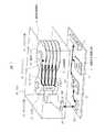
まず、図1により、本発明の一実施の形態の磁気ディスク装置の構成の一例を説明する。図1は磁気ディスク装置の構成図を示す。
【0020】
本実施の形態の磁気ディスク装置は、例えばHDA(ヘッド・ディスク・アセンブリ)10と、記録再生制御回路11などから構成される。
【0021】
HDA10は、磁気記録媒体13を積層したスピンドル部12と、磁気記録媒体13に対して情報を記録再生する磁気ヘッド14などを搭載したキャリッジ部15で構成され、アルミ製のベースとカバーで囲った構造のものである。
【0022】
キャリッジ部15は、磁気ヘッド14を磁気記録媒体13上でシークおよび位置決めさせるためのVCM(ボイスコイルモータ)17と、アーム18と、アーム18の先端に取付けたサスペンション19と、サスペンション19の先端に取付けた磁気ヘッド14と、記録再生信号を伝送するFPC(フレキシブル・パターンド・ケーブル)16と、FPC16に搭載したR/WIC内のプリアンプ20と、プリアンプ20と磁気ヘッド14間の記録再生信号を伝送する伝送線路21で構成されている。
【0023】
HDA10と外部装置との間には、記録再生制御回路11がある。この記録再生制御回路11は、HDA10の内部に設けられてもよい。記録再生制御回路11には、信号処理LSI22とHDD(ハードディスクドライブ)コントローラ23が搭載されている。HDA10側のコネクタ25−1と記録再生制御回路11側のコネクタ25−2を接続することにより、プリアンプ20と信号処理LSI22が接続される。記録再生制御回路11の外部インタフェース24を介して、外部装置と接続されるようになっている。
【0024】
次に、図2を用いて、本実施の形態の磁気ディスク装置において、アーム・サスペンション上の伝送線路の配置の一例を説明する。図2はアーム・サスペンション上の伝送線路の配置の平面図を示す。
【0025】
図2に示すように、プリアンプ20から磁気ヘッド14へ至る伝送線路21は、アーム18の横に沿って配置され、サスペンション19上にはプリント形成して設けられている。プリント形成した伝送線路21の先端には、記録ヘッド用コイル端子14W、再生ヘッドの出力端子14Rなどが設けられた磁気ヘッド14が接続されている。また、伝送線路21の他端には、記録アンプ20W、再生アンプ20Rからなるプリアンプ20が接続されている。
【0026】
この伝送線路21は、記録側線路21Wと再生側線路21Rが並走している並走部と、分離している分離部からなり、プリント形成されたサスペンション19上における並走部の記録側線路21Wと再生側線路21Rの位置関係および構造は、後述する図3〜図5に示すようになる。
【0027】
ここで、磁気ディスク装置における情報の記録動作、再生動作について説明する。
【0028】
一般的に、情報の記録は次のように行う。まず、上位装置から入力された情報を磁気記録再生に適したパターンデータに変換する。次に、パターンデータの‘1’に記録電流の極性反転を対応させ、データ‘0’には無反転を対応させる。パターンデータに極性反転電流を対応させた記録電流をプリアンプ20の記録アンプ20Wから記録側線路21Wに出力する。この記録電流は記録側線路21Wを通り、磁気ヘッド14の記録ヘッド用コイル端子14Wに達する。
【0029】
そして、記録ヘッド用コイル端子14Wから磁気ヘッド14の内部の記録磁界発生用コイルへ通電され、電流の極性に対応した磁界の方向を持つ記録磁界を発生する。磁気記録媒体13には、データパターン‘1’に対応した電流の反転、すなわち磁化反転を記録し、データパターン‘0’では電流の無反転、すなわち無磁化反転を記録する。
【0030】
一方、記録情報の再生は、磁気記録媒体13の磁化方向を磁気ヘッド14内の再生ヘッド(MRヘッド)が感知し、電圧の変化としてプリアンプ20に入力する。このプリアンプ20では、再生アンプ20Rで増幅した再生信号をチャネルLSIへ送り、データパターンをデコードすることにより、記録情報を再生する。
【0031】
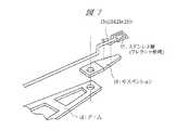
次に、図3〜図7を用いて、サスペンション上の伝送線路の構造の一例を説明する。図3〜図5はサスペンション上の伝送線路の構造の断面図を示し、それぞれ、図3は3層構造、図4は4層構造、図5は5層構造の例であり、また、(a)はカバー有り、(b)はカバーなしの例である。図6および図7はHGA(ヘッド・ジンバル・アセンブリ)の構造の説明図を示し、それぞれ、図6は図3、図7は図4および図5の例である。
【0032】
図3(a)に示す、サスペンション上の伝送線路21aは、記録側線路21Wと再生側線路21Rが所定の間隔で配置され、それぞれ、一対の記録側導体30、一対の再生側導体31からなる。これらの記録側導体30、再生側導体31は、下部導体34の上部に積層された絶縁層33の上に配置され、カバー32により覆われた構造でプリント形成されている。なお、図3(b)のように、カバー32のない伝送線路21bとすることも可能である。
【0033】
この伝送線路21a(21b)において、特に記録側導体30および再生側導体31の下層に絶縁層33を挟んで設けられた下部導体34は、厚さが5μm程度の銅または銅を主成分とする銅合金から形成されている。この下部導体34は、電気的にグランド電位となっている。また、絶縁層33は、厚さが5〜10μm程度のポリイミド樹脂から形成されている。なお、サスペンション19はステンレス、カバー32はポリイミド樹脂などからそれぞれ形成されている。
【0034】
このように、記録側導体30および再生側導体31、絶縁層33、下部導体34からなる3層構造の伝送線路21a(21b)の場合には、図6に示すように、アーム18の一端とサスペンション19の一端(磁気ヘッドと反対側)が接合され、この接合されたアーム18、サスペンション19上に伝送線路21a(21b)が実装された構造となる。この伝送線路21a(21b)の実装構造の場合、伝送線路21a(21b)はサスペンション19上に、例えば接着剤による実装となるために、サスペンション19への実装ばらつきが生じることがある。そこで、図4に示す構造が考えられる。
【0035】
図4(a)に示す、サスペンション19上の伝送線路21cは、前記図3の構造に加えて、下部導体34の下層に、ステンレス層35が設けられている。この4層構造の伝送線路21cの場合には、図7に示すように、ステンレス層35はフレクシャとして形成され、サスペンション19と合体される。なお、この構造においても、図4(b)のように、カバー32のない伝送線路21dとすることも可能である。
【0036】
この伝送線路21c(21d)の形成は、例えば伝送線路21cの全面の大きさのステンレス層35の上に、下部導体34、絶縁層33、記録側導体30および再生側導体31、カバー32(伝送線路21dはカバー無し)を順に積層してプリント形成した後、ステンレス層35のフレクシャとなる部分以外を切断して取り除くことにより形成することができる。
【0037】
この伝送線路21c(21d)の実装構造の場合、ステンレス層35とサスペンション19を、例えばポイント溶接にて実装することにより、実装ばらつきを低減できる。よって、ポイント溶接により頑強に、かつ低ばらつきで実装できる。さらに、サスペンション19、溶接点、ステンレス層35、下部導体34とグランドを共通にできるため、低周波数の雑音除去に効果がある。この構造において低周波雑音が混入する場合には、図5に示す構造としてもよい。
【0038】
図5(a)に示す、サスペンション19上の伝送線路21eは、前記図4の構造に加えて、下部導体34の下層に、ポリイミド樹脂から形成された絶縁層36を挟んでステンレス層35が設けられている。この5層構造の伝送線路21eの場合にも、前記図4の例と同様に、図7に示すように、ステンレス層35はフレクシャとして形成され、サスペンション19と合体される。なお、この構造においても、図5(b)のように、カバー32のない伝送線路21fとすることも可能である。この伝送線路21e(21f)の形成においても、前記図4と同様に形成することができる。
【0039】
この伝送線路21e(21f)の実装構造の場合、下部導体34の下に絶縁層36を挟み、絶縁層36の下にステンレス層35を設け、ステンレス層35とサスペンション19を、例えばポイント溶接にて実装することにより、下部導体34をグランドから離すことができる。よって、ポイント溶接により頑強に、かつ低ばらつきで実装できる。さらに、下部導体34をグランドから離すことができるので、低周波数の雑音の混入を防止できる。
【0040】
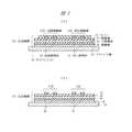
次に、図8〜図10を用いて、伝送線路の下部導体に銅またはステンレスを用いた場合の、消費電力の膜厚依存性をシミュレーションした結果の一例を説明する。図8〜図10は下部導体の膜厚に対する電力変化の特性図を示し、それぞれ絶縁層のポリイミド樹脂の膜厚が、図8は5μm、図9は10μm、図10は18μmの例である。
【0041】
図8に示すように、絶縁層33のポリイミド樹脂の膜厚が5μmの例で、下部導体34に銅(導電率σ=5.8E+07(=5.8×10⁷)〔S/m〕)を用いた場合には、膜厚が0.5μm程度では電力が120W程度であるが、2μm程度では35W程度、5μm程度では30W程度まで減少し、それ以上の膜厚では30W程度でほぼ一定となる。これに対して、下部導体34にステンレス(導電率σ=1.1E+06(=1.1×106)〔S/m〕)を用いた場合には、逆に、膜厚が0.5μm程度では電力が30W程度であるが、2μm程度では100W程度、5μm程度では150W程度まで増加し、10μm程度では140W程度、20μm程度では110W程度となる。これにより、ステンレスに比べて、銅を用いた場合には、膜厚を2μm程度以上にしても電力が低減できることが分かった。ステンレス層が薄い場合は、電力は小さくなるが、伝送線路としては使用できない理由を後程詳述する。
【0042】
図9は、絶縁層33のポリイミド樹脂の厚さが10μmの例であるが、この例でも、下部導体34にステンレスを用いた場合に比べて、銅を用いた場合には、膜厚が2μm程度以上では電力を25W程度まで減少し、前記図8の例に比べてさらに電力が低減できることが分かった。
【0043】
図10は、絶縁層33のポリイミド樹脂の厚さが18μmの例であるが、この例でも、下部導体34に銅を用いた場合には、膜厚が2μm程度以上では電力をさらに10W程度まで減少できることが分かった。
【0044】
このように、下部導体34にステンレスに代えて銅を用いた場合には、膜厚を薄くしても消費電力が低減できることが分かった。これは伝送線路の伝送損失の低減につながる。
【0045】
次に、図11〜図13を用いて、伝送線路の下部導体に銅またはステンレスを用いた場合の、下部導体の消費電力が最小になる導電率と膜厚との関係をシミュレーションした結果の一例を説明する。図11〜図13は下部導体の導電率と膜厚との関係の特性図を示し、それぞれ絶縁層のポリイミド樹脂の膜厚が、図11は5μm、図12は10μm、図13は18μmの例である。
【0046】
図11に示すように、絶縁層33のポリイミド樹脂の膜厚が5μmの例で、下部導体34に導電率σ=5.8E+07〔S/m〕の銅を用いた場合には、下部導体34の消費電力が最小になる膜厚の下限は2μm程度、上限は12μm程度となる。この膜厚の下限、上限の決定方法については、図14を用いて後述する。これに対して、下部導体34に導電率σ=1.1E+06〔S/m〕のステンレスを用いた場合には、下部導体34の消費電力が最小になる膜厚の下限および上限は31μm程度となる。これにより、ステンレスに比べて、銅を用いた場合には、膜厚を2〜12μm程度にすることで消費電力が最小にできることが分かった。
【0047】
図12は絶縁層33のポリイミド樹脂の厚さが10μmの例、図13は18μmの例であるが、これらの例でも、下部導体34にステンレスを用いた場合に比べて、銅を用いた場合には、膜厚を2〜15μm程度にすることで消費電力が最小にできることが分かった。
【0048】
次に、図14を用いて、下部導体の消費電力が最小になる膜厚の下限および上限の決定方法の一例を説明する。図14は伝送線路の伝送導体に高周波電流を流したときの下部導体に発生する誘導電流の状態の説明図を示す。
【0049】
図14に示すシミュレーションにおいては、一対の記録側導体30、一対の再生側導体31のうち、一対の記録側導体30の伝送導体に1GHzの電流(差動電流:例えば左側の導体には奥から手前への方向、右側の導体には逆に手前から奥への方向)を流した例で、下部導体34は導電率σ=5.8E+07〔S/m〕、すなわち銅を表したものである。なお、一対の再生側導体31の伝送導体においても同様である。
【0050】
図14において、一対の記録側導体30のような伝送導体に1GHzの高周波電流を流すと、その電流は表面部分(A部)に集中して流れる。この伝送導体に電流が流れると、絶縁層33を挟んで面している下部導体34には誘導電流が流れる。その流れる方法は、伝送導体に流れる電流と反対の方向である。誘導電流の分布は、伝送導体に近い部分ほど大きくなる。
【0051】
図14は、下部導体34が膜厚が厚い場合(10μm)を示している。図14のように、下部導体34が厚い場合は、誘導電流は下部導体34のうち、伝送導体に近い部分(B部)に集中して流れ、誘導電流が流れる部分のさらに下部(C部)には、図14のように、誘導電流とは逆方向の誘導電流が流れ始める。このC部に流れる誘導電流を2次誘導電流と定義する。
【0052】
一方、下部導体34の膜厚が薄い場合(5μm)は、厚い場合と同様に、伝送導体を流れる電流の誘導電流が下部導体34の伝送導体に近い部分に流れる。しかし、下部導体34が薄いために、誘導電流が流れると、下部導体34の全面を流れ、2次誘導電流が流れる領域がないために、2次誘導電流は流れない。
【0053】
ここでは、下部導体34で発生する伝送損失は、下部導体34で消費するエネルギー、すなわち発生する電力損失と定義している。従って、微小領域の電流(i)の自乗に微小領域の抵抗(r)を乗じて計算できる微小領域での消費電力(p)を、下部導体34の体積領域で合算した値が総消費電力(P)になる。
【0054】
従って、2次誘導電流が流れると、その流れただけ、消費電力が発生することになる。ゆえに、下部導体34の膜厚を厚くする方向で、2次誘導電流が流れ始めるときが、下部導体34の膜厚の上限となる。
【0055】
逆に、下部導体34の膜厚を薄くすると、伝送導体の電流に対応した誘導電流を流す領域がなくなり、誘導電流が流れなくなる。誘導電流が流れないので、消費電力は少なくなるが、十分な誘導電流が流れていないために、伝送導体の高周波電流と誘導電流とのカップリングが少なくなる。その結果、伝送導体間の相互インダクタンスが小さくなり、等価的に線路の特性インピーダンスが高くなって見える。すなわち、伝送線路の高周波信号領域では、異なる特性インピーダンスの線路をバイパスして通っている状態となり、伝送歪みの原因にもなる。従って、消費電力は低減するが、伝送特性は悪くなるために伝送線路としては好ましくない。従って、消費電力がピークになるときの下部導体34の膜厚が下限になる。
【0056】
また、図14の誘導電流の幅方向の広がりを見ると、線路導体幅以上に広がっている。そこで、シミュレーション結果から幅方向の広がり範囲を求めると、導体と導体の間隔の半分の幅が導体端面から広がっていることが分かった。従って、下層導体の幅は、少なくとも一対の導体幅と導体間隔の和より大きいことが必要であり、一対の導体幅の2倍あれば十分である。
【0057】
次に、図15を用いて、絶縁層のポリイミド樹脂の膜厚に依存する下部導体の導電率に対する最小消費電力の関係をシミュレーションした結果の一例を説明する。図15は下部導体の導電率に対する最小消費電力の関係の特性図を示す。
【0058】
図15に示すように、絶縁層33のポリイミド樹脂の膜厚が5μmの例では、下部導体34にステンレス(導電率σ=1.1E+06〔S/m〕)を用いた場合には110W程度の電力が消費されるのに対して、銅(導電率σ=5.8E+07〔S/m〕)を用いた場合には30W程度の電力の消費で済む。
【0059】
同様に、絶縁層33のポリイミド樹脂の膜厚が10μmの例では、70W程度から20W程度に消費電力を低減でき、ポリイミド樹脂の膜厚が18μmの例では、45W程度から10W程度に消費電力を低減することができる。
【0060】
以上説明した図8〜図15に示すシミュレーションの結果から、下部導体34に銅を使用することにより、従来は25μmの膜厚のステンレスを使用したものであるのに対して、5μmの膜厚の銅にしても伝送損失を低減できる。なお、銅の膜厚は、シミュレーションの結果から2〜12μm程度の範囲内に設定しても、伝送損失の低減効果は期待できる。
【0061】
また、記録側導体30および再生側導体31と下部導体34との間隔を決める絶縁層33の膜厚を、従来の10μmに対して、5〜10μmまで薄くすると伝送損失が増加するが、線路が薄くなるために伝送線路の剛性が低減でき、ヘッド周りの配線部へも適用できる。さらに、ヘッド周りの線路でのインピーダンスミスマッチを解消でき、伝送帯域の拡大が図れる。
【0062】
従って、本実施の形態の磁気ディスク装置によれば、以下のような効果を得ることができる。
【0063】
(1)サスペンション19上の伝送線路21a,21bが、記録側導体30および再生側導体31、絶縁層33、下部導体34からなる3層構造の場合に、下部導体34を銅にすることにより、下部導体34の誘導電流による電力消費を低減して線路の伝送損失を低減でき、かつ線路の厚さを薄くしてヘッド周りの配線部における剛性を低減することができる。
【0064】
(2)サスペンション19上の伝送線路21c,21dが、記録側導体30および再生側導体31、絶縁層33、下部導体34、ステンレス層35からなる4層構造の場合には、前記(1)と同様の効果に加えて、ステンレス層35とサスペンション19をポイント溶接にて実装することにより、頑強に、かつ低ばらつきで実装することができ、さらにサスペンション19、ステンレス層35、下部導体34とグランドを共通にできるため、低周波数の雑音を除去することができる。
【0065】
(3)サスペンション19上の伝送線路21e,21fが、記録側導体30および再生側導体31、絶縁層33、下部導体34、絶縁層36、ステンレス層35からなる5層構造の場合には、前記(1)と同様の効果に加えて、下部導体34の下に絶縁層36を挟んでステンレス層35を設け、ステンレス層35とサスペンション19とのポイント溶接により、頑強に、かつ低ばらつきで実装することができ、さらに下部導体34をグランドから離すことができるので、低周波数の雑音の混入を防止することができる。
【0066】
【発明の効果】
本発明によれば、伝送線路における伝送損失を低減することによって電気特性を向上させることができ、かつヘッド周りの配線部における剛性を低減することによって振動特性を向上させることができるので、電気特性の向上と振動特性の向上との両立によって伝送線路のインピーダンスフラット化を実現することが可能となる。
【図面の簡単な説明】
【図1】本発明の一実施の形態の磁気ディスク装置を示す構成図である。
【図2】本発明の一実施の形態の磁気ディスク装置において、アーム・サスペンション上の伝送線路の配置を示す平面図である。
【図3】(a),(b)は本発明の一実施の形態の磁気ディスク装置において、サスペンション上の伝送線路の構造(3層構造)を示す断面図である。
【図4】(a),(b)は本発明の一実施の形態の磁気ディスク装置において、サスペンション上の伝送線路の構造(4層構造)を示す断面図である。
【図5】(a),(b)は本発明の一実施の形態の磁気ディスク装置において、サスペンション上の伝送線路の構造(5層構造)を示す断面図である。
【図6】本発明の一実施の形態の磁気ディスク装置において、図3の例のHGAの構造を示す説明図である。
【図7】本発明の一実施の形態の磁気ディスク装置において、図4および図5の例のHGAの構造を示す説明図である。
【図8】本発明の一実施の形態の磁気ディスク装置において、下部導体の膜厚に対する電力変化(ポリイミド樹脂の膜厚=5μm)を示す特性図である。
【図9】本発明の一実施の形態の磁気ディスク装置において、下部導体の膜厚に対する電力変化(ポリイミド樹脂の膜厚=10μm)を示す特性図である。
【図10】本発明の一実施の形態の磁気ディスク装置において、下部導体の膜厚に対する電力変化(ポリイミド樹脂の膜厚=18μm)を示す特性図である。
【図11】本発明の一実施の形態の磁気ディスク装置において、下部導体の導電率と膜厚との関係(ポリイミド樹脂の膜厚=5μm)を示す特性図である。
【図12】本発明の一実施の形態の磁気ディスク装置において、下部導体の導電率と膜厚との関係(ポリイミド樹脂の膜厚=10μm)を示す特性図である。
【図13】本発明の一実施の形態の磁気ディスク装置において、下部導体の導電率と膜厚との関係(ポリイミド樹脂の膜厚=18μm)を示す特性図である。
【図14】本発明の一実施の形態の磁気ディスク装置において、伝送線路の伝送導体に高周波電流を流したときの下部導体に発生する誘導電流の状態を示す説明図である。
【図15】本発明の一実施の形態の磁気ディスク装置において、下部導体の導電率に対する最小消費電力の関係を示す特性図である。
【符号の説明】
10…HDA、13…磁気記録媒体、14…磁気ヘッド、14W…記録ヘッド用コイル端子、14R…再生ヘッドの出力端子、15…キャリッジ部、16…FPC、18…アーム、19…サスペンション、20…プリアンプ、20W…記録アンプ、20R…再生アンプ、21,21a,21b,21c,21d,21e,21f…伝送線路、21W…記録側線路、21R…再生側線路、30…記録側導体、31…再生側導体、32…カバー、33…絶縁層、34…下部導体、35…ステンレス層、36…絶縁層。[0001]
BACKGROUND OF THE INVENTION
The present invention relates to a magnetic disk device, and more particularly to a technique that is effective when applied to a transmission line structure that is mounted on a suspension and transmits a recording / reproducing signal to / from a magnetic head.
[0002]
[Prior art]
According to a study by the present inventor, the following techniques can be considered for the transmission line structure of the magnetic disk device.
[0003]
For example, in a magnetic disk device, in order to record a large amount of data in a limited space and record and reproduce a large amount of data in a short time, a high recording density technology and a high-speed data transfer technology, that is, a recording / reproducing frequency Higher frequency is essential.
[0004]
Some of such magnetic disk devices have a structure in which a transmission line for transmitting a recording / reproducing signal to and from a magnetic head is printed and mounted on a suspension. This transmission line is composed of a recording side line made of a pair of conductors and a reproduction side line made of a pair of conductors. A lower conductor is provided below the conductors of the recording side line and the reproduction side line with an insulating layer interposed therebetween.
[0005]
In such a transmission line, conventionally, the conductor of the recording side line and the reproducing side line is formed of copper with a thickness of about 15 μm, and the lower conductor is formed of stainless steel with a thickness of about 25 μm. The polyimide resin is formed with a thickness of about 10 μm.
[0006]
Further, for example, in
[0007]
[Patent Document 1]
JP 2002-237006 A
[0008]
[Problems to be solved by the invention]
By the way, as a result of the study of the transmission line structure of the magnetic disk device as described above, the following has been clarified.
[0009]
For example, the conventional transmission line as described above has a problem that transmission loss increases because the lower conductor below the conductors of the recording side line and the reproduction side line is made of stainless steel.
[0010]
Further, in the magnetic disk apparatus, it is necessary to reduce the rigidity of the wiring portion around the head and improve the followability of the magnetic head to the surface shape of the magnetic recording medium. However, when the thickness of the plate member made of copper is set to an upper limit of about 500 μm as in
[0011]
Further, in the conventional transmission line as described above, if the lower conductor made of stainless steel is thinned in order to be applied to the wiring portion around the head, the loss is increased. This phenomenon will be described in detail later.
[0012]
Therefore, in the conventional transmission line as described above and the technique as described in
[0013]
Accordingly, an object of the present invention is to achieve both an improvement in electrical characteristics by reducing transmission loss in the transmission line and an improvement in vibration characteristics by reducing rigidity in the wiring portion around the head, thereby realizing flattening of the impedance of the transmission line. It is an object of the present invention to provide a magnetic disk device that can perform the above-described operation.
[0014]
[Means for Solving the Problems]
In order to achieve the above object, the present invention mounts a magnetic head for recording / reproducing information on a magnetic recording medium, a transmission line for transmitting a recording / reproducing signal between the magnetic head, and the transmission line. The transmission line structure on the suspension is applied to a magnetic disk device having a suspension and has the following characteristics.
[0015]
(1) The transmission line mounted on the suspension is composed of a recording side line composed of a pair of conductors and a reproduction side line composed of a pair of conductors, and an insulating layer is provided below the recording side line and the conductors of the reproduction side line. A lower conductor is provided on both sides, and this lower conductor is made of copper having a thickness of about 5 μm or a copper alloy containing copper as a main component. Furthermore, the insulating layer is formed from a polyimide resin having a thickness of about 5 to 10 μm, and the lower conductor is electrically at ground potential.
[0016]
(2) In the above (1), a stainless steel layer is provided in the lower layer of the lower conductor, and this stainless steel layer is formed as a flexure and united with the suspension.
[0017]
(3) In the above (1), a stainless steel layer is provided below the lower conductor with an insulating layer in between, and this stainless steel layer is formed as a flexure and united with a suspension.
[0018]
DETAILED DESCRIPTION OF THE INVENTION
Hereinafter, embodiments of the present invention will be described in detail with reference to the drawings. Note that components having the same function are denoted by the same reference symbols throughout the drawings for describing the embodiments, and the repetitive description thereof will be omitted.
[0019]
First, an example of the configuration of a magnetic disk device according to an embodiment of the present invention will be described with reference to FIG. FIG. 1 is a configuration diagram of a magnetic disk device.
[0020]
The magnetic disk device according to the present embodiment includes, for example, an HDA (head disk assembly) 10 and a recording /
[0021]
The HDA 10 includes a spindle unit 12 on which a magnetic recording medium 13 is stacked, and a
[0022]
The
[0023]
A recording / reproducing
[0024]
Next, an example of the arrangement of transmission lines on the arm suspension in the magnetic disk device of the present embodiment will be described with reference to FIG. FIG. 2 shows a plan view of the arrangement of transmission lines on the arm suspension.
[0025]
As shown in FIG. 2, the transmission line 21 from the
[0026]
The transmission line 21 includes a parallel portion where the recording-
[0027]
Here, information recording and reproducing operations in the magnetic disk device will be described.
[0028]
In general, information is recorded as follows. First, information input from a host device is converted into pattern data suitable for magnetic recording and reproduction. Next, the polarity inversion of the recording current is associated with the pattern data “1”, and the non-inversion is associated with the data “0”. A recording current in which the polarity reversal current corresponds to the pattern data is output from the recording amplifier 20W of the
[0029]
The recording head coil terminal 14W is energized to the recording magnetic field generating coil in the magnetic head 14 to generate a recording magnetic field having a magnetic field direction corresponding to the polarity of the current. The magnetic recording medium 13 records current inversion corresponding to the data pattern “1”, that is, magnetization reversal, and the data pattern “0” records no current inversion, that is, no magnetization reversal.
[0030]
On the other hand, in reproducing recorded information, the reproducing head (MR head) in the magnetic head 14 senses the magnetization direction of the magnetic recording medium 13 and inputs it to the
[0031]
Next, an example of the structure of the transmission line on the suspension will be described with reference to FIGS. 3 to 5 are sectional views of the structure of the transmission line on the suspension. FIG. 3 is an example of a three-layer structure, FIG. 4 is a four-layer structure, and FIG. 5 is an example of a five-layer structure. ) Is an example with a cover, and (b) is an example without a cover. 6 and 7 are explanatory views of the structure of an HGA (Head Gimbal Assembly). FIG. 6 is an example of FIG. 3 and FIG. 7 is an example of FIGS.
[0032]
The transmission line 21a on the suspension shown in FIG. 3A includes a recording-
[0033]
In this transmission line 21a (21b), the
[0034]
Thus, in the case of the transmission line 21a (21b) having a three-layer structure comprising the
[0035]
The
[0036]
The
[0037]
In the case of the mounting structure of the
[0038]
In addition to the structure shown in FIG. 4, the transmission line 21e on the
[0039]
In the case of the mounting structure of the transmission line 21e (21f), an insulating layer 36 is sandwiched under the
[0040]
Next, an example of the result of simulating the film thickness dependence of power consumption when copper or stainless steel is used for the lower conductor of the transmission line will be described with reference to FIGS. 8 to 10 are graphs showing characteristics of power change with respect to the film thickness of the lower conductor. The film thickness of the polyimide resin of the insulating layer is 5 μm, FIG. 9 is 10 μm, and FIG. 10 is 18 μm, respectively.
[0041]
As shown in FIG. 8, in the example in which the film thickness of the polyimide resin of the insulating
[0042]
FIG. 9 shows an example in which the thickness of the polyimide resin of the insulating
[0043]
FIG. 10 shows an example in which the thickness of the polyimide resin of the insulating
[0044]
Thus, it has been found that when copper is used for the
[0045]
Next, an example of the result of simulating the relationship between the conductivity and the film thickness at which the power consumption of the lower conductor is minimized when copper or stainless steel is used for the lower conductor of the transmission line, using FIGS. Will be explained. FIGS. 11 to 13 are characteristic diagrams showing the relationship between the conductivity and film thickness of the lower conductor. The film thickness of the polyimide resin of the insulating layer is 5 μm in FIG. 11, 10 μm in FIG. 12, and 18 μm in FIG. It is.
[0046]
As shown in FIG. 11, in the case where the film thickness of the polyimide resin of the insulating
[0047]
FIG. 12 shows an example in which the thickness of the polyimide resin of the insulating
[0048]
Next, an example of a method for determining the lower limit and the upper limit of the film thickness that minimizes the power consumption of the lower conductor will be described with reference to FIG. FIG. 14 is an explanatory diagram showing the state of the induced current generated in the lower conductor when a high-frequency current is passed through the transmission conductor of the transmission line.
[0049]
In the simulation shown in FIG. 14, the transmission conductor of the pair of
[0050]
In FIG. 14, when a high frequency current of 1 GHz is passed through a transmission conductor such as a pair of recording-
[0051]
FIG. 14 shows a case where the
[0052]
On the other hand, when the film thickness of the
[0053]
Here, the transmission loss generated in the
[0054]
Therefore, when the secondary induced current flows, power consumption is generated as long as the second induced current flows. Therefore, the upper limit of the thickness of the
[0055]
On the other hand, when the thickness of the
[0056]
Further, when the spread in the width direction of the induced current in FIG. 14 is seen, it is wider than the line conductor width. Therefore, when the spread range in the width direction was determined from the simulation results, it was found that half the width between the conductors spread from the conductor end face. Therefore, the width of the lower layer conductor needs to be at least larger than the sum of the pair of conductor widths and the conductor interval, and it is sufficient if it is twice the width of the pair of conductors.
[0057]
Next, an example of the result of simulating the relationship of the minimum power consumption to the conductivity of the lower conductor depending on the film thickness of the polyimide resin of the insulating layer will be described with reference to FIG. FIG. 15 is a characteristic diagram showing the relationship of the minimum power consumption to the conductivity of the lower conductor.
[0058]
As shown in FIG. 15, in the case where the film thickness of the polyimide resin of the insulating
[0059]
Similarly, in the case where the film thickness of the polyimide resin of the insulating
[0060]
From the simulation results shown in FIGS. 8 to 15 described above, by using copper for the
[0061]
If the thickness of the insulating
[0062]
Therefore, according to the magnetic disk device of the present embodiment, the following effects can be obtained.
[0063]
(1) When the transmission lines 21a and 21b on the
[0064]
(2) When the
[0065]
(3) When the
[0066]
【The invention's effect】
According to the present invention, electrical characteristics can be improved by reducing transmission loss in the transmission line, and vibration characteristics can be improved by reducing rigidity in the wiring portion around the head. It is possible to realize impedance flattening of the transmission line by coexistence of improvement in the vibration characteristics and improvement in vibration characteristics.
[Brief description of the drawings]
FIG. 1 is a configuration diagram showing a magnetic disk device according to an embodiment of the present invention;
FIG. 2 is a plan view showing the arrangement of transmission lines on the arm suspension in the magnetic disk apparatus according to the embodiment of the present invention.
FIGS. 3A and 3B are cross-sectional views showing a structure (three-layer structure) of a transmission line on a suspension in a magnetic disk device according to an embodiment of the present invention. FIGS.
FIGS. 4A and 4B are cross-sectional views showing the structure (four-layer structure) of a transmission line on a suspension in a magnetic disk apparatus according to an embodiment of the present invention. FIGS.
FIGS. 5A and 5B are cross-sectional views showing the structure (5-layer structure) of a transmission line on a suspension in a magnetic disk apparatus according to an embodiment of the present invention. FIGS.
6 is an explanatory diagram showing the structure of the HGA in the example of FIG. 3 in the magnetic disk apparatus according to the embodiment of the invention. FIG.
7 is an explanatory diagram showing the structure of the HGA in the example of FIGS. 4 and 5 in the magnetic disk device according to the embodiment of the present invention. FIG.
FIG. 8 is a characteristic diagram showing a power change (polyimide resin film thickness = 5 μm) with respect to the film thickness of the lower conductor in the magnetic disk apparatus according to the embodiment of the present invention.
FIG. 9 is a characteristic diagram showing a power change (polyimide resin film thickness = 10 μm) with respect to the film thickness of the lower conductor in the magnetic disk apparatus according to the embodiment of the present invention.
10 is a characteristic diagram showing a change in power with respect to the film thickness of the lower conductor (polyimide resin film thickness = 18 μm) in the magnetic disk apparatus according to the embodiment of the present invention. FIG.
FIG. 11 is a characteristic diagram showing the relationship between the conductivity of the lower conductor and the film thickness (polyimide resin film thickness = 5 μm) in the magnetic disk device of one embodiment of the present invention.
FIG. 12 is a characteristic diagram showing the relationship between the conductivity and film thickness of the lower conductor (polyimide resin film thickness = 10 μm) in the magnetic disk drive according to one embodiment of the present invention.
FIG. 13 is a characteristic diagram showing the relationship between the conductivity and film thickness of the lower conductor (polyimide resin film thickness = 18 μm) in the magnetic disk device according to the embodiment of the present invention.
FIG. 14 is an explanatory diagram showing a state of an induced current generated in the lower conductor when a high-frequency current is passed through the transmission conductor of the transmission line in the magnetic disk device according to the embodiment of the present invention.
FIG. 15 is a characteristic diagram showing the relationship of the minimum power consumption with respect to the conductivity of the lower conductor in the magnetic disk device of one embodiment of the present invention.
[Explanation of symbols]
DESCRIPTION OF
Claims (5)
Translated fromJapanese前記サスペンションに実装された前記伝送線路は、一対の導体からなる記録側線路と一対の導体からなる再生側線路とから構成され、
前記記録側線路および前記再生側線路の導体の下層には、絶縁層を挟んで下部導体が設けられ、
前記下部導体は、厚さが5μmの銅または銅を主成分とする銅合金から形成されていることを特徴とする磁気ディスク装置。A magnetic disk device comprising: a magnetic head for recording / reproducing information with respect to a magnetic recording medium; a transmission line for transmitting a recording / reproduction signal to / from the magnetic head; and a suspension for mounting the transmission line,
The transmission line mounted on the suspension is composed of a recording side line composed of a pair of conductors and a reproduction side line composed of a pair of conductors,
Under the conductor of the recording side line and the reproduction side line, a lower conductor is provided with an insulating layer in between,
2. The magnetic disk drive according to claim 1, wherein the lower conductor is made of copper having a thickness of 5 [mu] m or a copper alloy containing copper as a main component.
前記絶縁層は、厚さが5〜10μmのポリイミド樹脂から形成されていることを特徴とする磁気ディスク装置。The magnetic disk apparatus according to claim 1,
The magnetic disk apparatus according to claim 1, wherein the insulating layer is made of a polyimide resin having a thickness of 5 to 10 μm.
前記下部導体は、電気的にグランド電位とされていることを特徴とする磁気ディスク装置。The magnetic disk device according to claim 2,
The magnetic disk apparatus according to claim 1, wherein the lower conductor is electrically at a ground potential.
前記下部導体の下層には、ステンレス層が設けられ、
前記ステンレス層はフレクシャとして形成され、前記サスペンションと合体されていることを特徴とする磁気ディスク装置。The magnetic disk device according to claim 3, wherein
A stainless steel layer is provided under the lower conductor,
The magnetic disk apparatus, wherein the stainless steel layer is formed as a flexure and is united with the suspension.
前記下部導体の下層には、絶縁層を挟んでステンレス層が設けられ、
前記ステンレス層はフレクシャとして形成され、前記サスペンションと合体されていることを特徴とする磁気ディスク装置。The magnetic disk device according to claim 3, wherein
Under the lower conductor, a stainless steel layer is provided with an insulating layer in between,
The magnetic disk apparatus, wherein the stainless steel layer is formed as a flexure and is united with the suspension.
Priority Applications (4)
| Application Number | Priority Date | Filing Date | Title |
|---|---|---|---|
| JP2003170945AJP2005011387A (en) | 2003-06-16 | 2003-06-16 | Magnetic disk unit |
| TW092134224ATWI260596B (en) | 2003-06-16 | 2003-12-04 | Disk device |
| KR1020040021504AKR100547544B1 (en) | 2003-06-16 | 2004-03-30 | Magnetic disk device |
| US10/870,573US7319573B2 (en) | 2003-06-16 | 2004-06-16 | Magnetic disk drive having a suspension mounted transmission line including read and write conductors and a lower conductor |
Applications Claiming Priority (1)
| Application Number | Priority Date | Filing Date | Title |
|---|---|---|---|
| JP2003170945AJP2005011387A (en) | 2003-06-16 | 2003-06-16 | Magnetic disk unit |
Publications (1)
| Publication Number | Publication Date |
|---|---|
| JP2005011387Atrue JP2005011387A (en) | 2005-01-13 |
Family
ID=33509136
Family Applications (1)
| Application Number | Title | Priority Date | Filing Date |
|---|---|---|---|
| JP2003170945APendingJP2005011387A (en) | 2003-06-16 | 2003-06-16 | Magnetic disk unit |
Country Status (4)
| Country | Link |
|---|---|
| US (1) | US7319573B2 (en) |
| JP (1) | JP2005011387A (en) |
| KR (1) | KR100547544B1 (en) |
| TW (1) | TWI260596B (en) |
Cited By (25)
| Publication number | Priority date | Publication date | Assignee | Title |
|---|---|---|---|---|
| JP2006278734A (en)* | 2005-03-29 | 2006-10-12 | Nitto Denko Corp | Printed circuit board |
| JP2007019261A (en)* | 2005-07-07 | 2007-01-25 | Nitto Denko Corp | Printed circuit board |
| JP2007035868A (en)* | 2005-07-26 | 2007-02-08 | Nitto Denko Corp | Method for manufacturing printed circuit board |
| US7182606B2 (en) | 2005-03-02 | 2007-02-27 | Nitto Denko Corporation | Wired circuit board |
| JP2007088056A (en)* | 2005-09-20 | 2007-04-05 | Nitto Denko Corp | Printed circuit board |
| JP2007157836A (en)* | 2005-12-01 | 2007-06-21 | Nitto Denko Corp | Printed circuit board |
| JP2007158249A (en)* | 2005-12-08 | 2007-06-21 | Nitto Denko Corp | Wiring circuit board and manufacturing method thereof |
| WO2007094177A1 (en)* | 2006-02-15 | 2007-08-23 | Nippon Steel Materials Co., Ltd. | Stainless steel substrate with conductive metal layer, hard disk suspension material and hard disk suspension manufactured by using the material |
| EP1883283A1 (en)* | 2006-07-28 | 2008-01-30 | Nitto Denko Corporation | Wired Circuit Board |
| JP2008060263A (en)* | 2006-08-30 | 2008-03-13 | Nitto Denko Corp | Wiring circuit board and manufacturing method thereof |
| JP2008084907A (en)* | 2006-09-26 | 2008-04-10 | Nitto Denko Corp | Printed circuit board |
| JP2008103745A (en)* | 2007-11-12 | 2008-05-01 | Nitto Denko Corp | Method for manufacturing printed circuit board |
| JP2008109147A (en)* | 2007-11-12 | 2008-05-08 | Nitto Denko Corp | Printed circuit board |
| EP1991040A2 (en) | 2007-05-10 | 2008-11-12 | Nitto Denko Corporation | Wired Circuit Board |
| EP2012566A2 (en) | 2007-07-05 | 2009-01-07 | Nitto Denko Corporation | Wired circuit board and producing method thereof |
| JP2010067317A (en)* | 2008-09-11 | 2010-03-25 | Dainippon Printing Co Ltd | Substrate for suspension |
| US7895741B2 (en) | 2007-07-24 | 2011-03-01 | Nitto Denko Corporation | Method of producing a wired circuit board |
| US8063312B2 (en) | 2006-09-27 | 2011-11-22 | Nitto Denko Corporation | Wired circuit board and producing method thereof |
| JP2012089232A (en)* | 2006-10-25 | 2012-05-10 | Nitto Denko Corp | Bonding method for flexure to flex printed circuit, and the flexure |
| JP2012155835A (en)* | 2012-03-16 | 2012-08-16 | Nitto Denko Corp | Suspension substrate with circuit |
| US8587903B2 (en) | 2011-11-22 | 2013-11-19 | Tdk Corporation | Suspension with high conductivity ground layer |
| US8693143B2 (en) | 2011-11-22 | 2014-04-08 | Tdk Corporation | Suspension with high conductivity ground layer for microwave signal transmission line, for magnetic head slider |
| US8730619B2 (en) | 2010-11-09 | 2014-05-20 | Dai Nippon Printing Co., Ltd. | Suspension substrate, suspension, element-mounted suspension, hard disk drive, and manufacturing method of suspension substrate |
| US8749923B2 (en) | 2008-12-22 | 2014-06-10 | Dai Nippon Printing Co., Ltd. | Suspension substrate, suspension, suspension with head and hard disk drive |
| JP2016021273A (en)* | 2015-09-07 | 2016-02-04 | 大日本印刷株式会社 | Substrate for suspension, suspension, suspension with head, and hard disk drive |
Families Citing this family (86)
| Publication number | Priority date | Publication date | Assignee | Title |
|---|---|---|---|---|
| KR100612886B1 (en)* | 2005-01-04 | 2006-08-14 | 삼성전자주식회사 | Flexibility of Hard Disk Drives Impedance Discontinuity Reduction Structure in Printed Circuits and Its Impedance Reduction Method |
| WO2006109507A1 (en)* | 2005-03-31 | 2006-10-19 | Nippon Steel Chemical Co., Ltd. | Laminate for hdd suspension and process for producing the same |
| JP2007272984A (en)* | 2006-03-31 | 2007-10-18 | Hitachi Global Storage Technologies Netherlands Bv | Disk drive device and head assembly used therefor |
| GB0718706D0 (en) | 2007-09-25 | 2007-11-07 | Creative Physics Ltd | Method and apparatus for reducing laser speckle |
| US7697237B1 (en)* | 2007-01-11 | 2010-04-13 | Hutchinson Technology Incorporated | Shielded copper-dielectric flexure for disk drive head suspensions |
| US7903376B2 (en)* | 2007-04-16 | 2011-03-08 | Hitachi Global Storage Technologies Netherlands, B.V. | Integrated lead suspension for vibration damping in magnetic storage device |
| JP2009026875A (en)* | 2007-07-18 | 2009-02-05 | Nitto Denko Corp | Printed circuit board |
| JP5142951B2 (en)* | 2008-11-10 | 2013-02-13 | 日東電工株式会社 | Wiring circuit board and manufacturing method thereof |
| US8289656B1 (en) | 2008-11-19 | 2012-10-16 | Western Digital Technologies, Inc. | Disk drive comprising stacked and stepped traces for improved transmission line performance |
| US8045297B2 (en)* | 2008-11-25 | 2011-10-25 | Hitachi Global Storage Technologies, Netherlands B.V. | Flex cable and method for lowering flex cable impedance |
| US9335604B2 (en) | 2013-12-11 | 2016-05-10 | Milan Momcilo Popovich | Holographic waveguide display |
| US11726332B2 (en) | 2009-04-27 | 2023-08-15 | Digilens Inc. | Diffractive projection apparatus |
| JP5134580B2 (en)* | 2009-05-01 | 2013-01-30 | 日東電工株式会社 | WIRING CIRCUIT BOARD AND MAGNETIC HEAD DRIVE DEVICE HAVING THE SAME |
| US8462466B2 (en)* | 2009-08-31 | 2013-06-11 | Western Digital Technologies, Inc. | Disk drive comprising impedance discontinuity compensation for interconnect transmission lines |
| US10795160B1 (en) | 2014-09-25 | 2020-10-06 | Rockwell Collins, Inc. | Systems for and methods of using fold gratings for dual axis expansion |
| US11300795B1 (en) | 2009-09-30 | 2022-04-12 | Digilens Inc. | Systems for and methods of using fold gratings coordinated with output couplers for dual axis expansion |
| US8233204B1 (en) | 2009-09-30 | 2012-07-31 | Rockwell Collins, Inc. | Optical displays |
| US11320571B2 (en) | 2012-11-16 | 2022-05-03 | Rockwell Collins, Inc. | Transparent waveguide display providing upper and lower fields of view with uniform light extraction |
| US8310789B2 (en)* | 2009-12-22 | 2012-11-13 | Hitachi Global Storage Technologies Netherlands B.V. | Conductor suspension structure and electrical connection assembly for transmitting complementary signals in a hard disk drive |
| US8659826B1 (en) | 2010-02-04 | 2014-02-25 | Rockwell Collins, Inc. | Worn display system and method without requiring real time tracking for boresight precision |
| CN102194468B (en)* | 2010-03-19 | 2015-08-12 | 新科实业有限公司 | Cantilever part, magnetic head folding piece combination with same and hard disk drive |
| US8467151B1 (en) | 2010-05-21 | 2013-06-18 | Western Digital Technologies, Inc. | Disk drive comprising an interconnect with transmission lines forming an approximated lattice network |
| US8598460B2 (en) | 2010-12-22 | 2013-12-03 | HGST Netherlands B.V. | Interleaved conductor structure with offset traces |
| US8675311B2 (en) | 2010-12-22 | 2014-03-18 | HGST Netherlands B.V. | Interleaved conductor structure with wrap around traces |
| WO2012136970A1 (en) | 2011-04-07 | 2012-10-11 | Milan Momcilo Popovich | Laser despeckler based on angular diversity |
| US10670876B2 (en) | 2011-08-24 | 2020-06-02 | Digilens Inc. | Waveguide laser illuminator incorporating a despeckler |
| WO2016020630A2 (en) | 2014-08-08 | 2016-02-11 | Milan Momcilo Popovich | Waveguide laser illuminator incorporating a despeckler |
| EP2995986B1 (en) | 2011-08-24 | 2017-04-12 | Rockwell Collins, Inc. | Data display |
| US9366864B1 (en) | 2011-09-30 | 2016-06-14 | Rockwell Collins, Inc. | System for and method of displaying information without need for a combiner alignment detector |
| US9507150B1 (en) | 2011-09-30 | 2016-11-29 | Rockwell Collins, Inc. | Head up display (HUD) using a bent waveguide assembly |
| US9715067B1 (en) | 2011-09-30 | 2017-07-25 | Rockwell Collins, Inc. | Ultra-compact HUD utilizing waveguide pupil expander with surface relief gratings in high refractive index materials |
| US8903207B1 (en) | 2011-09-30 | 2014-12-02 | Rockwell Collins, Inc. | System for and method of extending vertical field of view in head up display utilizing a waveguide combiner |
| US8634139B1 (en) | 2011-09-30 | 2014-01-21 | Rockwell Collins, Inc. | System for and method of catadioptric collimation in a compact head up display (HUD) |
| US8749890B1 (en) | 2011-09-30 | 2014-06-10 | Rockwell Collins, Inc. | Compact head up display (HUD) for cockpits with constrained space envelopes |
| US8937772B1 (en) | 2011-09-30 | 2015-01-20 | Rockwell Collins, Inc. | System for and method of stowing HUD combiners |
| US8488279B1 (en) | 2011-11-22 | 2013-07-16 | Western Digital (Fremont), Llc | Disk drive suspension assembly with flexure having stacked interleaved traces |
| US20150010265A1 (en) | 2012-01-06 | 2015-01-08 | Milan, Momcilo POPOVICH | Contact image sensor using switchable bragg gratings |
| US9523852B1 (en) | 2012-03-28 | 2016-12-20 | Rockwell Collins, Inc. | Micro collimator system and method for a head up display (HUD) |
| US8830588B1 (en) | 2012-03-28 | 2014-09-09 | Rockwell Collins, Inc. | Reflector and cover glass for substrate guided HUD |
| CN106125308B (en) | 2012-04-25 | 2019-10-25 | 罗克韦尔柯林斯公司 | Device and method for displaying images |
| US9933684B2 (en) | 2012-11-16 | 2018-04-03 | Rockwell Collins, Inc. | Transparent waveguide display providing upper and lower fields of view having a specific light output aperture configuration |
| US9674413B1 (en) | 2013-04-17 | 2017-06-06 | Rockwell Collins, Inc. | Vision system and method having improved performance and solar mitigation |
| WO2015015138A1 (en) | 2013-07-31 | 2015-02-05 | Milan Momcilo Popovich | Method and apparatus for contact image sensing |
| US8879212B1 (en) | 2013-08-23 | 2014-11-04 | Western Digital Technologies, Inc. | Disk drive suspension assembly with flexure having dual conductive layers with staggered traces |
| US9244281B1 (en) | 2013-09-26 | 2016-01-26 | Rockwell Collins, Inc. | Display system and method using a detached combiner |
| EP2884289A1 (en)* | 2013-12-10 | 2015-06-17 | ams AG | Chip scale current sensor package and method of producing a current sensor package |
| US9275664B2 (en)* | 2013-12-13 | 2016-03-01 | HGST Netherlands B.V. | Shielded flex cable for use in a disk drive |
| US10732407B1 (en) | 2014-01-10 | 2020-08-04 | Rockwell Collins, Inc. | Near eye head up display system and method with fixed combiner |
| US9519089B1 (en) | 2014-01-30 | 2016-12-13 | Rockwell Collins, Inc. | High performance volume phase gratings |
| US9064513B1 (en) | 2014-03-07 | 2015-06-23 | Western Digital Technologies, Inc. | Disk drive suspension assembly with flexure having dual conductive layers with staggered traces |
| US9244280B1 (en) | 2014-03-25 | 2016-01-26 | Rockwell Collins, Inc. | Near eye display system and method for display enhancement or redundancy |
| US10359736B2 (en) | 2014-08-08 | 2019-07-23 | Digilens Inc. | Method for holographic mastering and replication |
| WO2016042283A1 (en) | 2014-09-19 | 2016-03-24 | Milan Momcilo Popovich | Method and apparatus for generating input images for holographic waveguide displays |
| US9715110B1 (en) | 2014-09-25 | 2017-07-25 | Rockwell Collins, Inc. | Automotive head up display (HUD) |
| US10088675B1 (en) | 2015-05-18 | 2018-10-02 | Rockwell Collins, Inc. | Turning light pipe for a pupil expansion system and method |
| WO2016113534A1 (en) | 2015-01-12 | 2016-07-21 | Milan Momcilo Popovich | Environmentally isolated waveguide display |
| US9632226B2 (en) | 2015-02-12 | 2017-04-25 | Digilens Inc. | Waveguide grating device |
| US10126552B2 (en) | 2015-05-18 | 2018-11-13 | Rockwell Collins, Inc. | Micro collimator system and method for a head up display (HUD) |
| US11366316B2 (en) | 2015-05-18 | 2022-06-21 | Rockwell Collins, Inc. | Head up display (HUD) using a light pipe |
| US10247943B1 (en) | 2015-05-18 | 2019-04-02 | Rockwell Collins, Inc. | Head up display (HUD) using a light pipe |
| US10108010B2 (en) | 2015-06-29 | 2018-10-23 | Rockwell Collins, Inc. | System for and method of integrating head up displays and head down displays |
| CN113759555B (en) | 2015-10-05 | 2024-09-20 | 迪吉伦斯公司 | Waveguide Display |
| US10598932B1 (en) | 2016-01-06 | 2020-03-24 | Rockwell Collins, Inc. | Head up display for integrating views of conformally mapped symbols and a fixed image source |
| CN108780224B (en) | 2016-03-24 | 2021-08-03 | 迪吉伦斯公司 | Method and apparatus for providing a polarization selective holographic waveguide device |
| US10890707B2 (en) | 2016-04-11 | 2021-01-12 | Digilens Inc. | Holographic waveguide apparatus for structured light projection |
| WO2018102834A2 (en) | 2016-12-02 | 2018-06-07 | Digilens, Inc. | Waveguide device with uniform output illumination |
| US10545346B2 (en) | 2017-01-05 | 2020-01-28 | Digilens Inc. | Wearable heads up displays |
| US10295824B2 (en) | 2017-01-26 | 2019-05-21 | Rockwell Collins, Inc. | Head up display with an angled light pipe |
| WO2019079350A2 (en) | 2017-10-16 | 2019-04-25 | Digilens, Inc. | Systems and methods for multiplying the image resolution of a pixelated display |
| US10732569B2 (en) | 2018-01-08 | 2020-08-04 | Digilens Inc. | Systems and methods for high-throughput recording of holographic gratings in waveguide cells |
| WO2019136476A1 (en) | 2018-01-08 | 2019-07-11 | Digilens, Inc. | Waveguide architectures and related methods of manufacturing |
| EP3710876A4 (en) | 2018-01-08 | 2022-02-09 | DigiLens Inc. | SYSTEMS AND METHODS OF FABRICATING WAVEGUIDE CELLS |
| EP3710894B1 (en) | 2018-01-08 | 2025-07-30 | Digilens Inc. | Methods for fabricating optical waveguides |
| FR3080699B1 (en)* | 2018-04-27 | 2020-05-15 | Ingenico Group | SECURITY SYSTEM FOR A MAGNETIC CARD READER, CORRESPONDING MAGNETIC CARD READER AND ELECTRONIC DEVICE. |
| WO2020023779A1 (en) | 2018-07-25 | 2020-01-30 | Digilens Inc. | Systems and methods for fabricating a multilayer optical structure |
| US20200225471A1 (en) | 2019-01-14 | 2020-07-16 | Digilens Inc. | Holographic Waveguide Display with Light Control Layer |
| US20200247017A1 (en) | 2019-02-05 | 2020-08-06 | Digilens Inc. | Methods for Compensating for Optical Surface Nonuniformity |
| US20220283377A1 (en) | 2019-02-15 | 2022-09-08 | Digilens Inc. | Wide Angle Waveguide Display |
| KR102866596B1 (en) | 2019-02-15 | 2025-09-29 | 디지렌즈 인코포레이티드. | Method and device for providing a holographic waveguide display using an integral grating |
| WO2020186113A1 (en) | 2019-03-12 | 2020-09-17 | Digilens Inc. | Holographic waveguide backlight and related methods of manufacturing |
| EP3980825A4 (en) | 2019-06-07 | 2023-05-03 | Digilens Inc. | WAVEGUIDES WITH TRANSMITTING AND REFLECTING GRIDS AND RELATED MANUFACTURING PROCESSES |
| EP4004646A4 (en) | 2019-07-29 | 2023-09-06 | Digilens Inc. | METHODS AND APPARATUS FOR MULTIPLYING THE IMAGE RESOLUTION AND FIELD OF VIEW OF A PIXELATED DISPLAY SCREEN |
| KR102775783B1 (en) | 2019-08-29 | 2025-02-28 | 디지렌즈 인코포레이티드. | Vacuum grid and method for manufacturing the same |
| WO2022150841A1 (en) | 2021-01-07 | 2022-07-14 | Digilens Inc. | Grating structures for color waveguides |
| US12158612B2 (en) | 2021-03-05 | 2024-12-03 | Digilens Inc. | Evacuated periodic structures and methods of manufacturing |
| JP2024046955A (en)* | 2022-09-26 | 2024-04-05 | 日東電工株式会社 | Method for manufacturing a printed circuit board, and printed circuit board |
Family Cites Families (16)
| Publication number | Priority date | Publication date | Assignee | Title |
|---|---|---|---|---|
| JP3580893B2 (en) | 1995-03-24 | 2004-10-27 | 日東電工株式会社 | Suspension wiring board for magnetic head |
| US5608591A (en)* | 1995-06-09 | 1997-03-04 | International Business Machines Corporation | Integrated head-electronics interconnection suspension for a data recording disk drive |
| US6942817B2 (en)* | 2000-03-24 | 2005-09-13 | Dainippon Printing Co., Ltd. | Method of manufacturing wireless suspension blank |
| US6700748B1 (en)* | 2000-04-28 | 2004-03-02 | International Business Machines Corporation | Methods for creating ground paths for ILS |
| US6480359B1 (en)* | 2000-05-09 | 2002-11-12 | 3M Innovative Properties Company | Hard disk drive suspension with integral flexible circuit |
| JP2002237016A (en) | 2001-02-09 | 2002-08-23 | Tdk Corp | Head gimbals assembly |
| JP4277455B2 (en)* | 2001-02-27 | 2009-06-10 | Tdk株式会社 | Head gimbal assembly |
| US6894875B2 (en)* | 2001-04-18 | 2005-05-17 | Dai Nippon Printing Co., Ltd. | Magnetic head suspension with both protected wiring and unprotected wiring, in addition to terminals |
| WO2003023768A1 (en)* | 2001-09-05 | 2003-03-20 | Seagate Technology Llc | Flex on suspension with actuator dynamic function |
| US6757137B1 (en)* | 2001-09-30 | 2004-06-29 | Magnecomp Corporation | Stiffness controlled disk drive suspension with limiter feature |
| US6943302B2 (en)* | 2002-01-07 | 2005-09-13 | Achilles Corporation | Flexible printed circuit board |
| JP3929319B2 (en)* | 2002-02-01 | 2007-06-13 | 富士通株式会社 | Suspension and magnetic recording / reading apparatus |
| US6785094B2 (en)* | 2002-04-24 | 2004-08-31 | Hitachi Global Storage Technologies | Weld free high performance laminate suspension |
| US7079357B1 (en)* | 2002-04-30 | 2006-07-18 | Magnecomp Corporation | Additive-process suspension interconnect with controlled noise |
| US7158348B2 (en)* | 2002-05-01 | 2007-01-02 | Hitachi Global Storage Technologies Netherlands B.V. | Integrated lead suspension for use in a disk drive using a tri-metal laminate and method for fabrication |
| US7161767B2 (en)* | 2002-07-16 | 2007-01-09 | Sae Magnetics (H.K.) Ltd. | Wireless suspension design with ground plane structure |
- 2003
- 2003-06-16JPJP2003170945Apatent/JP2005011387A/enactivePending
- 2003-12-04TWTW092134224Apatent/TWI260596B/ennot_activeIP Right Cessation
- 2004
- 2004-03-30KRKR1020040021504Apatent/KR100547544B1/ennot_activeExpired - Fee Related
- 2004-06-16USUS10/870,573patent/US7319573B2/ennot_activeExpired - Fee Related
Cited By (37)
| Publication number | Priority date | Publication date | Assignee | Title |
|---|---|---|---|---|
| US7182606B2 (en) | 2005-03-02 | 2007-02-27 | Nitto Denko Corporation | Wired circuit board |
| JP2006278734A (en)* | 2005-03-29 | 2006-10-12 | Nitto Denko Corp | Printed circuit board |
| JP2007019261A (en)* | 2005-07-07 | 2007-01-25 | Nitto Denko Corp | Printed circuit board |
| US8134080B2 (en) | 2005-07-07 | 2012-03-13 | Nitto Denko Corporation | Wired circuit board |
| JP2007035868A (en)* | 2005-07-26 | 2007-02-08 | Nitto Denko Corp | Method for manufacturing printed circuit board |
| JP2007088056A (en)* | 2005-09-20 | 2007-04-05 | Nitto Denko Corp | Printed circuit board |
| JP2007157836A (en)* | 2005-12-01 | 2007-06-21 | Nitto Denko Corp | Printed circuit board |
| US7638873B2 (en) | 2005-12-01 | 2009-12-29 | Nitto Denko Corporation | Wired circuit board |
| JP2007158249A (en)* | 2005-12-08 | 2007-06-21 | Nitto Denko Corp | Wiring circuit board and manufacturing method thereof |
| US7501581B2 (en) | 2005-12-08 | 2009-03-10 | Nitto Denko Corporation | Wired circuit board and producing method thereof |
| WO2007094177A1 (en)* | 2006-02-15 | 2007-08-23 | Nippon Steel Materials Co., Ltd. | Stainless steel substrate with conductive metal layer, hard disk suspension material and hard disk suspension manufactured by using the material |
| JP2007220785A (en)* | 2006-02-15 | 2007-08-30 | Nippon Steel Materials Co Ltd | Stainless steel substrate with conductive metal layer, manufacturing method thereof, hard disk suspension material, and hard disk suspension |
| EP1883283A1 (en)* | 2006-07-28 | 2008-01-30 | Nitto Denko Corporation | Wired Circuit Board |
| US8266794B2 (en) | 2006-08-30 | 2012-09-18 | Nitto Denko Corporation | Method of producing a wired circuit board |
| EP1895820A3 (en)* | 2006-08-30 | 2009-08-05 | Nitto Denko Corporation | Wired circuit board and production method thereof |
| JP2008060263A (en)* | 2006-08-30 | 2008-03-13 | Nitto Denko Corp | Wiring circuit board and manufacturing method thereof |
| US7723617B2 (en) | 2006-08-30 | 2010-05-25 | Nitto Denko Corporation | Wired circuit board and production method thereof |
| JP2008084907A (en)* | 2006-09-26 | 2008-04-10 | Nitto Denko Corp | Printed circuit board |
| US8101863B2 (en) | 2006-09-26 | 2012-01-24 | Nitto Denko Corporation | Printed circuit board |
| US8327535B2 (en) | 2006-09-27 | 2012-12-11 | Nitto Denko Corporation | Wired circuit board and producing method thereof |
| US8063312B2 (en) | 2006-09-27 | 2011-11-22 | Nitto Denko Corporation | Wired circuit board and producing method thereof |
| JP2012089232A (en)* | 2006-10-25 | 2012-05-10 | Nitto Denko Corp | Bonding method for flexure to flex printed circuit, and the flexure |
| EP1991040A2 (en) | 2007-05-10 | 2008-11-12 | Nitto Denko Corporation | Wired Circuit Board |
| US8760815B2 (en) | 2007-05-10 | 2014-06-24 | Nitto Denko Corporation | Wired circuit board |
| EP2012566A3 (en)* | 2007-07-05 | 2009-11-25 | Nitto Denko Corporation | Wired circuit board and producing method thereof |
| EP2012566A2 (en) | 2007-07-05 | 2009-01-07 | Nitto Denko Corporation | Wired circuit board and producing method thereof |
| US8354597B2 (en) | 2007-07-05 | 2013-01-15 | Nitto Denko Corporation | Wired circuit board and producing method thererof |
| US7895741B2 (en) | 2007-07-24 | 2011-03-01 | Nitto Denko Corporation | Method of producing a wired circuit board |
| JP2008109147A (en)* | 2007-11-12 | 2008-05-08 | Nitto Denko Corp | Printed circuit board |
| JP2008103745A (en)* | 2007-11-12 | 2008-05-01 | Nitto Denko Corp | Method for manufacturing printed circuit board |
| JP2010067317A (en)* | 2008-09-11 | 2010-03-25 | Dainippon Printing Co Ltd | Substrate for suspension |
| US8749923B2 (en) | 2008-12-22 | 2014-06-10 | Dai Nippon Printing Co., Ltd. | Suspension substrate, suspension, suspension with head and hard disk drive |
| US8730619B2 (en) | 2010-11-09 | 2014-05-20 | Dai Nippon Printing Co., Ltd. | Suspension substrate, suspension, element-mounted suspension, hard disk drive, and manufacturing method of suspension substrate |
| US8587903B2 (en) | 2011-11-22 | 2013-11-19 | Tdk Corporation | Suspension with high conductivity ground layer |
| US8693143B2 (en) | 2011-11-22 | 2014-04-08 | Tdk Corporation | Suspension with high conductivity ground layer for microwave signal transmission line, for magnetic head slider |
| JP2012155835A (en)* | 2012-03-16 | 2012-08-16 | Nitto Denko Corp | Suspension substrate with circuit |
| JP2016021273A (en)* | 2015-09-07 | 2016-02-04 | 大日本印刷株式会社 | Substrate for suspension, suspension, suspension with head, and hard disk drive |
Also Published As
| Publication number | Publication date |
|---|---|
| KR100547544B1 (en) | 2006-01-31 |
| US20040252413A1 (en) | 2004-12-16 |
| TW200501082A (en) | 2005-01-01 |
| US7319573B2 (en) | 2008-01-15 |
| TWI260596B (en) | 2006-08-21 |
| KR20040108538A (en) | 2004-12-24 |
Similar Documents
| Publication | Publication Date | Title |
|---|---|---|
| JP2005011387A (en) | Magnetic disk unit | |
| US8467150B2 (en) | Recording head, disk drive with recording head, and recording method using recording head | |
| JP2007299460A (en) | Magnetic head, and magnetic recording and reproducing device | |
| JP2004259323A (en) | Magnetic disk drive | |
| JP4312968B2 (en) | Wiring member for disk drive suspension | |
| JP5226432B2 (en) | Magnetic head | |
| JP3931074B2 (en) | Signal transmission line, suspension and recording apparatus including the same | |
| JPH06274830A (en) | Thin-film magnetic head | |
| US9036306B1 (en) | Grounding for a hard disk drive suspension tail | |
| JP2006277864A (en) | Magnetic disk unit | |
| JPS61144712A (en) | Magnetic head | |
| JPH11306703A (en) | Wiring integrated suspension structure and head disk assembly using the same | |
| JP2007157209A (en) | Magnetic recording device | |
| JPH06162407A (en) | Magnetic head device | |
| JP2002352401A (en) | Composite thin film magnetic head and its manufacturing method | |
| US6563675B1 (en) | Magnetic head unit | |
| JP2672105B2 (en) | Magnetic head | |
| JPH0573831A (en) | Magnetic head | |
| JPH0294011A (en) | thin film magnetic head | |
| JPH06267027A (en) | Magnetoresistance effect type thin film magnetic head | |
| JPH10105917A (en) | Thin film magnetic head | |
| JPH0474302A (en) | Magnetic head | |
| JPH06195668A (en) | Head moving device | |
| JPS61144709A (en) | magnetic head | |
| JPS6157026A (en) | Magnetoresistance effect type head |
Legal Events
| Date | Code | Title | Description |
|---|---|---|---|
| A621 | Written request for application examination | Free format text:JAPANESE INTERMEDIATE CODE: A621 Effective date:20060609 | |
| A977 | Report on retrieval | Free format text:JAPANESE INTERMEDIATE CODE: A971007 Effective date:20080709 | |
| A131 | Notification of reasons for refusal | Free format text:JAPANESE INTERMEDIATE CODE: A131 Effective date:20080715 | |
| A521 | Written amendment | Free format text:JAPANESE INTERMEDIATE CODE: A523 Effective date:20080916 | |
| A02 | Decision of refusal | Free format text:JAPANESE INTERMEDIATE CODE: A02 Effective date:20081125 | |
| A521 | Written amendment | Free format text:JAPANESE INTERMEDIATE CODE: A523 Effective date:20090121 | |
| A521 | Written amendment | Free format text:JAPANESE INTERMEDIATE CODE: A523 Effective date:20090121 | |
| A911 | Transfer to examiner for re-examination before appeal (zenchi) | Free format text:JAPANESE INTERMEDIATE CODE: A911 Effective date:20090218 | |
| A131 | Notification of reasons for refusal | Free format text:JAPANESE INTERMEDIATE CODE: A131 Effective date:20090317 | |
| A912 | Re-examination (zenchi) completed and case transferred to appeal board | Free format text:JAPANESE INTERMEDIATE CODE: A912 Effective date:20090626 |