JP2004532562A - Coupling circuit for power line communication - Google Patents
Coupling circuit for power line communicationDownload PDFInfo
- Publication number
- JP2004532562A JP2004532562AJP2002578681AJP2002578681AJP2004532562AJP 2004532562 AJP2004532562 AJP 2004532562AJP 2002578681 AJP2002578681 AJP 2002578681AJP 2002578681 AJP2002578681 AJP 2002578681AJP 2004532562 AJP2004532562 AJP 2004532562A
- Authority
- JP
- Japan
- Prior art keywords
- inductive
- coupler
- signal
- data signal
- power line
- Prior art date
- Legal status (The legal status is an assumption and is not a legal conclusion. Google has not performed a legal analysis and makes no representation as to the accuracy of the status listed.)
- Pending
Links
- 238000010168coupling processMethods0.000titleclaimsabstractdescription37
- 230000008878couplingEffects0.000titleclaimsabstractdescription36
- 238000005859coupling reactionMethods0.000titleclaimsabstractdescription36
- 238000004891communicationMethods0.000titleclaimsabstractdescription27
- 230000001939inductive effectEffects0.000claimsabstractdescription77
- 239000004020conductorSubstances0.000claimsabstractdescription46
- 238000004804windingMethods0.000claimsabstractdescription44
- 239000003990capacitorSubstances0.000claimsabstractdescription31
- 238000000034methodMethods0.000claimsabstractdescription28
- 230000007935neutral effectEffects0.000claimsdescription16
- 238000001228spectrumMethods0.000claimsdescription10
- 238000011144upstream manufacturingMethods0.000claimsdescription4
- 230000001568sexual effectEffects0.000claims1
- 230000011664signalingEffects0.000claims1
- 238000010586diagramMethods0.000description14
- 230000002457bidirectional effectEffects0.000description3
- 230000000903blocking effectEffects0.000description2
- 230000003321amplificationEffects0.000description1
- 230000005540biological transmissionEffects0.000description1
- 230000009977dual effectEffects0.000description1
- 230000000694effectsEffects0.000description1
- 230000006698inductionEffects0.000description1
- 238000002955isolationMethods0.000description1
- 238000012986modificationMethods0.000description1
- 230000004048modificationEffects0.000description1
- 238000003199nucleic acid amplification methodMethods0.000description1
- 230000010355oscillationEffects0.000description1
Images


Classifications
- H—ELECTRICITY
- H04—ELECTRIC COMMUNICATION TECHNIQUE
- H04B—TRANSMISSION
- H04B3/00—Line transmission systems
- H04B3/54—Systems for transmission via power distribution lines
- H04B3/56—Circuits for coupling, blocking, or by-passing of signals
- H—ELECTRICITY
- H04—ELECTRIC COMMUNICATION TECHNIQUE
- H04B—TRANSMISSION
- H04B2203/00—Indexing scheme relating to line transmission systems
- H04B2203/54—Aspects of powerline communications not already covered by H04B3/54 and its subgroups
- H04B2203/5462—Systems for power line communications
- H04B2203/5466—Systems for power line communications using three phases conductors
- H—ELECTRICITY
- H04—ELECTRIC COMMUNICATION TECHNIQUE
- H04B—TRANSMISSION
- H04B2203/00—Indexing scheme relating to line transmission systems
- H04B2203/54—Aspects of powerline communications not already covered by H04B3/54 and its subgroups
- H04B2203/5462—Systems for power line communications
- H04B2203/5479—Systems for power line communications using repeaters
- H—ELECTRICITY
- H04—ELECTRIC COMMUNICATION TECHNIQUE
- H04B—TRANSMISSION
- H04B2203/00—Indexing scheme relating to line transmission systems
- H04B2203/54—Aspects of powerline communications not already covered by H04B3/54 and its subgroups
- H04B2203/5462—Systems for power line communications
- H04B2203/5483—Systems for power line communications using coupling circuits
- H—ELECTRICITY
- H04—ELECTRIC COMMUNICATION TECHNIQUE
- H04B—TRANSMISSION
- H04B2203/00—Indexing scheme relating to line transmission systems
- H04B2203/54—Aspects of powerline communications not already covered by H04B3/54 and its subgroups
- H04B2203/5462—Systems for power line communications
- H04B2203/5491—Systems for power line communications using filtering and bypassing
Landscapes
- Engineering & Computer Science (AREA)
- Power Engineering (AREA)
- Computer Networks & Wireless Communication (AREA)
- Signal Processing (AREA)
- Cable Transmission Systems, Equalization Of Radio And Reduction Of Echo (AREA)
Abstract
Translated fromJapaneseDescription
Translated fromJapanese【技術分野】
【0001】
本発明は、配電システムに対する通信信号の結合に関する。
【従来の技術】
【0002】
通信信号は広帯域電力線モデムを含む種々の装置により配電システムに結合されることができる。直交周波数分割多重(OFDM)または直接シーケンス拡散スペクトル(DSSS)のような多数の広帯域電力線モデムは拡散スペクトル変調技術を使用している。毎秒多メガビットのデータレートに対しては、そのようなモデムは1〜50MHzの範囲内の周波数帯域を使用する。拡散スペクトル変調の1つの利点は周波数帯域のあるセグメントを使用できないようにする共振および狭い帯域幅雑音に拘らずモデムに接続する能力である。しかし、そのような使用できない周波数帯域セグメントの数を減少させてそれによりデータレートを増加させ、エラーレートを低下させることが望ましい。
【0003】
拡散スペクトルモデムの信号出力は配電ラインに効率よく結合される必要がある。典型的に、これは配電用変成器(DT)の2次端子またはそれに近い接合点のようなラインが集中する点において生じる。しかしながら、駆動点インピーダンスとして知られているこの結合点のインピーダンスは、ある周波数帯域にわたる非常に低いインピーダンスから他の周波数帯域にわたる非常に高いインピーダンスまで広い範囲で変化する可能性がある。比較的簡単な結合技術はある周波数帯域では合理的な効率であるが、他の周波数帯域では大きい結合損失による減衰を導入する可能性がある。
【0004】
シャント結合は通常使用されている1つの技術であり、それにおいては、モデムは直列の阻止キャパシタによって電力線を横切って直接結合されている。図1Aおよび図1Bは従来の技術による配電システムに対するモデムのシャント容量性結合を示している。配電システムはインピーダンスZT108 を有する2次巻線130 を有する配電用変成器を含んでいる。モデムA110 は電力線115 および117 を横切って阻止キャパシタ113 を介して接続されて広帯域高周波数電流を与える。モデムA110 は内部抵抗RS112 を有している。
【発明の開示】
【発明が解決しようとする課題】
【0005】
図1Bにおいて、|ZT|<<RSである周波数帯域に対しては、ZT108 がモデムA110 の出力を重く負荷して実質的な結合損失を生じる。モデムA110 が低い出力インピーダンスであっても、インピーダンスZT108 が反射された負荷インピーダンスZLref(図示せず)よりも遥かに低いときには結合による減衰を受ける。そのような場合には、モデムA110 から導入された電流の大部分は低い大きさのインピーダンスZT108 を通って流れ、ほんの少しの部分だけがZLrefを通ってモデムB140 に向かって流れる。したがってシャント容量性結合は広範囲で変化する駆動点インピーダンスおよび非常に低いインピーダンスに対しては効率が悪い。
【課題を解決するための手段】
【0006】
本発明の例示的な実施形態は、シャントキャパシタを有する直列インダクタンスモード結合に基づいた配電システムにデータ信号を結合する方法および対応するシステムを含んでいる。誘導性信号結合器は2つの巻線を有している。第1の巻線は配電システムの電力線導体と直列である。キャパシタは、電力信号に対しては高いインピーダンスを与え、データ信号に対しては低いインピーダンスを与えるように配電システムの第1の電力線導体と第2の電力線導体との間に接続されている。通信装置は、通信装置と配電システムとの間にデータ信号が結合されることができるように第2の巻線に結合されている。
【0007】
さらに別の実施形態では、電力線導体は中性線導体である。通信装置は拡散スペクトルモデムであってもよい。誘導性信号結合器は、2次巻線が変成器の磁気コアに巻かれ、磁気コア内の電力線導体の一部が1次巻線として作用するように電力線導体にクランプされた分割された磁気コアを含んでいる。1次巻線は、データ信号の最高使用周波数の波長の1/10に等価な距離以内の位置で変成器の2次巻線に隣接して配置されるとよい。この位置は変成器の2次巻線の端子の位置に本質的に結合器を配置するような充分な近接した位置である。
【0008】
本発明の代表的な実施形態はまた、直列インダクタンスモード結合器および並列キャパシタンスモード結合器に基づいた配電システムにデータ信号を結合する方法および対応するシステムを含んでいる。直列インダクタンス結合器は配電システムの第1の電力線導体に接続されている。シャント容量性結合器は第1の電力線導体と第2の電力線導体との間に接続されている。通信装置は並列な第1と第2のインターフェースを有し、その第1のインターフェースは一方の結合器に接続され、第2のインターフェースは他方の結合器に接続されて通信装置と配電システムとの間のデータ信号の結合を可能にしている
さらに別の実施形態では、電力線導体は中性線導体である。通信装置は拡散スペクトルモデムであってもよい。誘導性信号結合器は第2の巻線が変成器の磁気コアに巻かれ、磁気コア内の電力線導体の一部が1次巻線として作用するように電力線導体にクランプされた分割された磁気コアを含んでいる。1次巻線は、データ信号の最高使用周波数の波長の1/10以内の距離で変成器の2次巻線に隣接して配置することができる。
【0009】
本発明の代表的な実施形態はまた、配電システムの低インピーダンスノードを横切ってデータ信号を結合する方法および対応するシステムを含んでいる。キャパシタは配電システムの低インピーダンスノードと並列に接続され、電力信号に対しては高いインピーダンスを与えデータ信号に対しては低いインピーダンスを与えている。第1の誘導性結合器はノードの上流で電力線導体と直列に接続されている。第2の誘導性結合器はノードの下流で電力線導体と直列に接続されている。第1の誘導性結合器と第2の誘導性結合器とはノードを横切ってデータ信号を結合させるように接続されている。
【0010】
さらに別の実施形態では、信号増幅器が第1の誘導性結合器と第2の誘導性結合器とを接続して動作させている。その代りに、或いはそれに付加して、データルータが第1の誘導性結合器と第2の誘導性結合器とを接続して第1の誘導性結合器と第2の誘導性結合器との間でデータ信号を選択的に導くように構成されることもできる。その場合には、第2の誘導性結合器はノードの下流の複数の誘導性結合器の1つであってもよく、それによりデータルータは第1の誘導性結合器と複数の誘導性結合器との間でデータ信号を選択的に導くことが可能になる。
【発明を実施するための最良の形態】
【0011】
本発明は、添付図面を参照にした以下の詳細な説明によりさらに容易に理解されるであろう。
本発明の代表的な実施形態は配電システムに広帯域の通信信号を結合する改良された直列インダクタンスに対する技術を使用する。中程度の電圧(MV)の配電ネットワークにおける直列インダクタンス結合に関する1つの方法は米国特許出願09/752,705号明細書(2000年12月28日出願)に記載されており、ここで参考文献とされる。シャント容量結合とは対照的に、直列インダクタンス結合は、モデムのインピーダンスに対する配電用変成器インピーダンスの負荷による信号減衰を避けることができる。
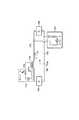
【0012】
図1Cは本発明の1実施例による改良された直列インダクタンス結合器の概略図を示しており、図1Dは等価回路を示している。誘導性結合器120 は配電用変成器(DT)135 付近において低電圧回路の中性線115 に直列に接続されて動作する。誘導性結合器120 は配電用変成器135 の2次巻線130 に近接して位置され、結合器120 によって中性線115 に結合される信号の最高使用周波数の波長の1/10以内の距離であることが好ましい。
【0013】
図1DからZT108 の低い値の絶対値が、結合器120 と、変成器2次巻線インピーダンスZT108 と、電力線115 および116 と、負荷インピーダンスZL160 およびモデムB140 の並列組合わせとを通って結合されているモデムA110 を含む回路中を電流が流れるのを容易にしている。図1Dの回路はまた反射された負荷インピーダンスZLrefl165 を含んでおり、それは駆動点に戻る電力線を通って反射される高周波負荷インピーダンスを表している。
【0014】
直列インダクタンス結合回路は、変成器2次巻線インピーダンスZT108 が関係する周波数帯域にわたって均一な低いインピーダンスであるときに特に良好である。しかしながら、高いインピーダンスZT108 はインピーダンスZT108 と反射された負荷インピーダンスZLrefl165 との直列の全体のインピーダンスを増加させ、それ故、電力線に結合されたモデム電流IL170 の量を減少させる。したがって直列インダクタンス結合器は非常に高い駆動点インピーダンスに対しては比較的効率が悪い。
【0015】
図1Eおよびその等価回路である図1Fは図1Cおよび図1Dに示された基本的な直列インダクタンスモード結合よりも、ZT108 の絶対値が高い周波数帯域においてさえも高い結合効率維持する実施例を示している。図1Eでは変成器135 の2次巻線130 と並列に配置された1以上のキャパシタ125 を有している。したがって、図1Fに示されているように、キャパシタ125 はZT108 と並列である。この並列結合は結果的にZT108 単独の場合よりも低い合成インピーダンスを与える。したがってモデム110 から結合さられる電流はZT108 のインピーダンスとは実質的に無関係となる。結合器120 は既存の電力線120Aの含まれた部分を含む直列インダクタンス結合器であり、それは1巻きの巻線と、ライン120Aの周囲に位置する分割磁気コア120Bと、磁気コア120Bに巻かれた2次巻線120Cとして機能する。
【0016】
キャパシタ125 が配電用変成器の2次巻線の両端間に並列に接続されたとき、モデムの周波数帯域にわたって変成器ま端子間の合成インピーダンスを低下させ、しかも、キャパシタ125 は配電電力周波数に対しては開回路として有効に作用する。例えば10nFのキャパシタのインピーダンスは1MHzでは16オームよりも低く、10MHz以上では1.6オームよりも低く、一方60Hzでは250kオームを越える高いインピーダンスである。
【0017】
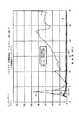
図2は典型的な配電用変成器の2次側における周波数の関数としてインピーダンスを示している。曲線Aはキャパシタのないインピーダンスを表しており、曲線Bは2次巻線と並列に10nFのキャパシタが接続された時の合成インピーダンスを表している。曲線Aは並列キャパシタのない2.8〜3.9MHzおよび16.3〜30MHzの周波数帯域の特性を示しており、インピーダンスは40オームを越えている。これは変成器の巻線または導線における並列共振による可能性がある。他方、曲線Bに示されるように、DTの2次巻線に並列に10nFのキャパシタが接続されたとき組合わされた並列インピーダンスは全ての周波数に対して10オーム以下である。
【0018】
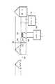
本発明の実施形態は単相電力回路およびYまたはデルタのいずれかの形態の多相電力回路の両者に適用可能である。2相電力ライン(図1Eに示されている)または3相Y接続電力ラインに対しては、結合器120 は中性線115 に配置されることが好ましい。この配置では、相ライン116 および117 は帰路電流がほぼ均等に分割されるRF帰路線路である。したがって、構内装置145 において、相ライン116 および117 の1つと中性線115 との間に接続されたモデムは類似した信号レベルを示す可能性が高い。これは単相ライン上に結合器120 を配置するのとは対照的であり、他の相の電力線がケーブルに沿って負荷に誘導だけによって各信号を得ることを可能にする。中性線115 上の誘導性結合器120 の配置はまた電力周波数電流レベル、すなわち配電システムにより与えられる結合器の磁気コア120B中の電流を減少させることにより磁気コアの飽和効果を最少にする。
【0019】
図1Gはデルタ接続された3相電力変成器170 および3相ライン175 、180 、185 を示している。結合器120 は3相ラインの1つ、例えばライン175 に配置され、残りの相のライン180 および185 は信号の帰路を与える。この配置は帰路電流の振幅の平衡を助ける。示されているように、1以上のキャパシタ125 が変成器170 の2次巻線と並列に付加されて、変成器170 の2次巻線のインピーダンスが高い周波数帯域の電流に対する低インピーダンス路を確保している。
【0020】
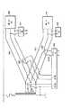
図3Aおよび3Bは本発明の実施形態による電力伝送ラインの両端における低インピーダンスノードをバイパスするための技術を示している。このような状態の例には、(a)多数の階層の建物でマスター電力パネルから個々のフロアの電力パネルに接続されているラインと、(b)ラインが低電圧配電ネットワークで1つのノードから他のノードに接続されているラインと、(c)変成器サブステーションからマルチライン接続点に接続されているMVラインとを含んでいる。図3Aは単相に簡単化された図1Eおよび図1Fで示されるように接続されたデータトランク303 上のモデムA110 を示している。変成器305 はMV−LVまたはLV−LV配電用変成器でよい。
【0021】
低インピーダンスのノードは負荷が回路に接続される方法によって生成される可能性がある。例えば、端子332 間に多数の負荷315 、320 、325 が接続され、並列インピーダンスを生成し、端子332 間に結果的な低い駆動点インピーダンスを生成する。その代りに、或いはそれに付加して低インピーダンスの装置333 が端子332 間に接続されて、下流の装置334 と通信するためのインピーダンスを表すこともできる。
【0022】
端子332 の対のような低インピーダンスノードは以下のようにバイパスされることができる。RF短絡キャパシタ360 は関係する周波数帯域にわたってその低インピーダンスを確保するために1対の端子332 間に接続される。信号は誘導性結合器365 および370 を介して端子332 をバイパスされる。結合器365 はキャパシタ360 の上流で中性線310 に取付けられることが好ましく、結合器370 は端子332 およびキャパシタ360 の下流に取付けられることが好ましい。端子332 間の低インピーダンスのために、モデムA110 から中性線310 を通って到着する信号電流の全ては基本的に結合器365 および帰路(例えば線311 )を通って流れる。端子332 間の低インピーダンスは端子332 の左側から来る信号と端子332 の右側の信号とを隔離する。
【0023】
結合器365 と370 との間の信号路は(a)受動的バイパスを表す直接接続であってもよく、或いは(b)両方向性信号増幅器のような能動モジュール375 を含む能動路であってもよく、データ中継器は入力と出力とが同じ周波数帯域にあってもよく、或いは入力と出力の周波数帯域が互いに異なっていてもよい。能動モジュール375 が両方向性ブースター増幅器を含む場合には、発振を阻止するためにキャパシタ360 により導入された減衰の大きさは能動モジュール375 の増幅度を超える必要がある。
【0024】
図3Bは、図3Aに示された装置のさらに強化された構成を示している。別々の下流の結合器385 が個々のラインに取付けられ、それぞれは1以上の負荷、例えば負荷315 、320 、325 に給電する。個々の各結合器385 はブースタまたは中継器、例えば、モジュール380 の別々のポートXX、YY、ZZにより駆動される。ポートXX、YY、ZZにおける各出力は同一の波形であってもよい。その代りに、モジュール380 はルータ機能を含んでいてもよく、別々のデータ流を各負荷負荷315 、320 、325 に与えてもよい。
【0025】
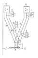
図4は共通の電力ラインコンバージェンスノードから異なる回路に別々のデータ流を送信する技術を示している。MV用において、変成器435 はサブステーションにおいて高電圧を中程度の電圧に変換する(HV−MV)変成器であり、ライン405 および410 は異なったMV回路への給電を示している。LV用においては、変成器435 はMV−LVまたはLV−LV配電用変成器を表しており、ライン405 および410 は異なった建物または建物内の異なったフロアを表している。
【0026】
例えば、LV配電を例として説明すると、図4はDT435 からスター形状で給電される多数の構内装置440 および445 を概略的に示している。しばしば多数の電力ケーブル405 および410 がDT435 の2次端子にボルトで取付けられ、或いはDT435 に近い接合ノードから分離されている。各ケーブルは分離された構内装置のセット440 および445 を給電するように接続されている。例えば電力ケーブル405 は構内装置445 に導かれ、電力ケーブル410 は構内装置440 に導かれる。図4には2つの電力ケーブル405 および410 が示されているが、スター形状では2本よりも多くの電力ケーブルが含まれることができる。
【0027】
キャパシタ125 および415 の付加的な利点は、電力ケーブル405 および410 によって給電される種々の2次負荷回路間の高周波数分離を与えることである。これは構内装置440 および445 のそれぞれににおけるユーザのセットに異なったフル帯域のデータ流を伝送する別々の媒体として機能することを可能にする。例えば、ケーブル410 においてはモデム1A425 はモデム1B426 と通信し、ケーブル405 においてモデム2A430 はモデム2B431 と通信する。
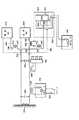
【0028】
図5はZLrefにおける種々の変化を克服する本発明の別の実施形態の概略図である。図を簡単にするために、図5では1つの方向の信号流だけを示しているが、システム自体は実際には両方向性である。モデムは内部インピーダンスRS1515 を有するソース発生器VS1510 からのシャント駆動を含み、それはシャントモードで電力線に実質的な信号電力を結合する。反射された負荷インピーダンスZLrefが比較的高い周波数範囲に対しては、シャント駆動は通信信号を送信する非常に効率のよいモードである。二重結合モードモデム505 は2つの出力回路を備え、それらは同一波形の、恐らく異なった振幅および、または異なったインピーダンスレベルの信号を与える。第1のシャントキャパシタ出力回路は内部インピーダンスRS1515 を有する発生器VS1510 を含み、第2の直列インダクタンス出力回路は内部インピーダンスRS2525 を有する発生器VS1520 を含んでいる。例えば、これらの出力回路は共通の信号源から駆動される2つの出力増幅器であることができる。
【0029】
図5は、結合キャパシタ530 を介してシャントモードでDTの2次巻線インピーダンス215 の端子を駆動する第1の出力回路を示している。第2の出力回路は第1の出力回路と同位相の直列モード誘導性結合器120 を駆動する。シャント容量性モードはインピーダンスZTおよびZLrefが共に比較的高い周波数範囲に対して効率のよい駆動を行う。直列インダクタンスモードはインピーダンスZLrefが比較的低い周波数範囲に対して特に効率がよい。シャントモードと直列モードとの組合わせはインピーダンス組合わせの広い範囲にわたって効率のよい駆動を与える。
【0030】
図6は本発明の別の実施形態を示しており、それにおいては多数の2次電力ライン605 および610 の場合に対してに組合わせたシャントおよび直列モードが使用されている。例えば中性線に類似した絶縁されたラインのグルーブが、例えば図1Cに示されるように単一の誘導性結合器120 を取付けることを阻止するように大きい直径であってもよい。したがって多数の結合器620 および622 は各中性線に対して1つづつ取付けられ、モデムA625 からの同じ波形により駆動されることができ、そのモデムA625 には多数の出力615A、615B、615Cを設けられている。出力615Aおよび随意のキャパシタ635 は全ての低電圧電力線と共通の単一のシャント駆動を行い、それらの低電圧電力線はモデムの単一周波数において相ラインを共に短絡し、それにより両方の相ラインが出力615Aによって駆動される。出力615Bおよび615Cはそれぞれ直列モードで単一の中性線を駆動する。したがってモデムA625 は全てのモデムB623 および631 との間でデータを送信および受信する。図6には2つの電力線を有する形態のシステムが示されているが、任意の適当な数のラインが含まれてもよい。
【0031】
本発明の種々の例示的な実施形態が開示されたが、本発明の幾つかの効果を達成するために種々の変形変更が本発明の技術的範囲を逸脱することなく行われることができることは当業者には明白である。
【図面の簡単な説明】
【0032】
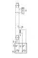
【図1A】従来技術による配電システムに対するモデムのシャント容量性結合を示す概略図。
【図1B】従来技術による配電システムに対するモデムのシャント容量性結合を示す概略図。
【図1C】本発明の1実施形態の配電システムに対するモデムの直列誘導性結合を示す概略図。
【図1D】本発明の1実施形態の配電システムに対するモデムの直列誘導性結合を示す概略図。
【図1E】本発明の1実施形態のシャントキャパシタを付加した直列誘導性結合を示す概略図。
【図1F】本発明の1実施形態のシャントキャパシタを付加した直列誘導性結合を示す概略図。
【図1G】3相配電システムの変成器にデルタ接続で結合された直列誘導性結合の1実施形態を示す概略図。
【図2】典型的な配電用変成器の2次側における周波数の関数としてのインピーダンスを示すグラフ。
【図3A】本発明の1実施形態による配電システムの低インピーダンスノードのバイパスを示す概略図。
【図3B】本発明の1実施形態による配電システムの低インピーダンスノードのバイパスを示す概略図。
【図4】共通の電力線コンバージェンスノードから異なる回路に別々のデータ流を送信する実施形態を示す概略図。
【図5】反射されたインピーダンスの変化を克服する1実施形態を示す概略図。
【図6】シャントおよび直列結合モードを組合わせて使用する1実施形態を示す概略図。【Technical field】
[0001]
The present invention relates to coupling communication signals to a power distribution system.
[Prior art]
[0002]
Communication signals can be coupled to a power distribution system by various devices, including a broadband power line modem. Many wideband power line modems, such as orthogonal frequency division multiplexing (OFDM) or direct sequence spread spectrum (DSSS), use spread spectrum modulation techniques. For data rates of many megabits per second, such modems use a frequency band in the range of 1-50 MHz. One advantage of spread spectrum modulation is the ability to connect to a modem despite resonances and narrow bandwidth noise that render certain segments of the frequency band unusable. However, it is desirable to reduce the number of such unusable frequency band segments, thereby increasing the data rate and reducing the error rate.
[0003]
The signal output of a spread spectrum modem needs to be efficiently coupled to a distribution line. Typically, this occurs at points where the lines are concentrated, such as at the secondary terminals of a distribution transformer (DT) or near junctions. However, the impedance of this junction, known as the driving point impedance, can vary widely from very low impedance over one frequency band to very high impedance over another frequency band. Relatively simple coupling techniques are reasonably efficient in some frequency bands, but can introduce significant coupling loss attenuation in other frequency bands.
[0004]
Shunt coupling is one commonly used technique, in which the modem is directly coupled across the power line by a series blocking capacitor. 1A and 1B show the shunt capacitive coupling of a modem to a prior art power distribution system. The power distribution system includes a power distribution transformer having a
DISCLOSURE OF THE INVENTION
[Problems to be solved by the invention]
[0005]
In FIG. 1B, for frequency bands where | ZT | << RS ,
[Means for Solving the Problems]
[0006]
Exemplary embodiments of the present invention include a method and a corresponding system for coupling a data signal to a power distribution system based on series inductance mode coupling with a shunt capacitor. The inductive signal combiner has two windings. The first winding is in series with the power line conductor of the power distribution system. The capacitor is connected between the first power line conductor and the second power line conductor of the power distribution system to provide a high impedance for the power signal and a low impedance for the data signal. The communication device is coupled to the second winding such that a data signal can be coupled between the communication device and the power distribution system.
[0007]
In yet another embodiment, the power line conductor is a neutral conductor. The communication device may be a spread spectrum modem. An inductive signal combiner has a split magnetic field in which a secondary winding is wound around the magnetic core of the transformer and a portion of the power line conductor in the magnetic core is clamped to the power line conductor to act as a primary winding. Contains core. The primary winding is preferably located adjacent to the secondary winding of the transformer at a position within a distance equivalent to 1/10 of the wavelength of the highest operating frequency of the data signal. This location is close enough to place the coupler essentially at the terminal of the secondary winding of the transformer.
[0008]
Exemplary embodiments of the present invention also include a method and corresponding system for coupling a data signal to a power distribution system based on a series inductance mode coupler and a parallel capacitance mode coupler. The series inductance coupler is connected to the first power line conductor of the power distribution system. The shunt capacitive coupler is connected between the first power line conductor and the second power line conductor. The communication device has a first and a second interface in parallel, the first interface being connected to one coupler and the second interface being connected to the other coupler to provide communication between the communication device and the power distribution system. In yet another embodiment that allows coupling of data signals between the power line conductors are neutral conductors. The communication device may be a spread spectrum modem. The inductive signal combiner has a split magnetic field in which a second winding is wound on the magnetic core of the transformer and a portion of the power line conductor in the magnetic core is clamped to the power line conductor to act as a primary winding. Contains core. The primary winding may be located adjacent to the secondary winding of the transformer at a distance within 1/10 of the wavelength of the highest operating frequency of the data signal.
[0009]
Exemplary embodiments of the present invention also include a method of coupling data signals across low impedance nodes of a power distribution system and a corresponding system. The capacitor is connected in parallel with the low impedance node of the power distribution system and provides a high impedance for power signals and a low impedance for data signals. The first inductive coupler is connected in series with the power line conductor upstream of the node. A second inductive coupler is connected in series with the power line conductor downstream of the node. The first inductive coupler and the second inductive coupler are connected to couple the data signal across the node.
[0010]
In yet another embodiment, a signal amplifier connects and operates the first inductive coupler and the second inductive coupler. Alternatively or additionally, a data router connects the first inductive coupler and the second inductive coupler to connect the first inductive coupler and the second inductive coupler. It can also be configured to selectively direct data signals between them. In that case, the second inductive coupler may be one of a plurality of inductive couplers downstream of the node, so that the data router is connected to the first inductive coupler with the plurality of inductive couplers. Data signals can be selectively guided to and from the device.
BEST MODE FOR CARRYING OUT THE INVENTION
[0011]
The present invention will be more readily understood from the following detailed description with reference to the accompanying drawings.
Exemplary embodiments of the present invention use techniques for improved series inductance to couple broadband communication signals into a power distribution system. One method for series inductance coupling in medium voltage (MV) distribution networks is described in US patent application Ser. No. 09 / 752,705, filed Dec. 28, 2000, which is hereby incorporated by reference. Is done. In contrast to shunt capacitive coupling, series inductance coupling can avoid signal attenuation due to the loading of the distribution transformer impedance on the modem impedance.
[0012]
FIG. 1C shows a schematic diagram of an improved series inductance coupler according to one embodiment of the present invention, and FIG. 1D shows an equivalent circuit. The
[0013]
Figures 1D absolute value of the low value of
[0014]
A series inductance coupling circuit is particularly good when the transformer secondary winding
[0015]
FIG. 1E and its equivalent circuit FIG. 1F show an embodiment that maintains higher coupling efficiency even in frequency bands where the absolute value of
[0016]
When
[0017]
FIG. 2 shows the impedance as a function of frequency on the secondary side of a typical distribution transformer. Curve A represents the impedance without a capacitor, and curve B represents the combined impedance when a 10 nF capacitor is connected in parallel with the secondary winding. Curve A shows the characteristics for the frequency bands 2.8-3.9 MHz and 16.3-30 MHz without parallel capacitors, with the impedance exceeding 40 ohms. This may be due to parallel resonance in the transformer windings or conductors. On the other hand, as shown by curve B, when a 10 nF capacitor is connected in parallel with the secondary winding of DT, the combined parallel impedance is less than 10 ohms for all frequencies.
[0018]
Embodiments of the present invention are applicable to both single-phase power circuits and polyphase power circuits in either the Y or delta form. For a two-phase power line (shown in FIG. 1E) or a three-phase Y-connected power line,
[0019]
FIG. 1G shows a delta-connected three-
[0020]
3A and 3B illustrate techniques for bypassing low impedance nodes at both ends of a power transmission line according to embodiments of the present invention. Examples of such conditions include (a) lines connected from the master power panel to the individual floor power panels in a multi-story building, and (b) lines connected from one node in a low voltage distribution network. And (c) an MV line connected from the transformer substation to the multiline connection point. FIG. 3A shows a single phase simplified modem A110 on a
[0021]
Low impedance nodes can be created by the way the load is connected to the circuit. For example, a number of
[0022]
Low impedance nodes, such as the pair of
[0023]
The signal path between the
[0024]
FIG. 3B shows a further enhanced configuration of the device shown in FIG. 3A. Separate
[0025]
FIG. 4 illustrates a technique for transmitting separate data streams from a common power line convergence node to different circuits. For MV,
[0026]
For example, taking LV power distribution as an example, FIG. 4 schematically illustrates a number of
[0027]
An additional advantage of
[0028]
FIG. 5 is a schematic diagram of another embodiment of the present invention that overcomes various changes in ZLref . For simplicity, FIG. 5 shows only one direction of signal flow, but the system itself is in fact bidirectional. The modem includes a shunt drive from a
[0029]
FIG. 5 shows the first output circuit driving the terminal of the secondary winding
[0030]
FIG. 6 shows another embodiment of the present invention, in which a combined shunt and series mode is used for the case of multiple
[0031]
While various exemplary embodiments of the invention have been disclosed, it is to be understood that various modifications can be made without departing from the scope of the invention, in order to achieve several advantages of the invention. It will be apparent to those skilled in the art.
[Brief description of the drawings]
[0032]
FIG. 1A is a schematic diagram illustrating shunt capacitive coupling of a modem to a power distribution system according to the prior art.
FIG. 1B is a schematic diagram illustrating shunt capacitive coupling of a modem to a power distribution system according to the prior art.
FIG. 1C is a schematic diagram illustrating serial inductive coupling of a modem to a power distribution system according to one embodiment of the present invention.
FIG. 1D is a schematic diagram illustrating serial inductive coupling of a modem to a power distribution system according to one embodiment of the present invention.
FIG. 1E is a schematic diagram illustrating a series inductive coupling with a shunt capacitor according to one embodiment of the present invention.
FIG. 1F is a schematic diagram showing a series inductive coupling to which a shunt capacitor according to one embodiment of the present invention is added.
FIG. 1G is a schematic diagram illustrating one embodiment of a series inductive coupling coupled in a delta connection to a transformer of a three-phase power distribution system.
FIG. 2 is a graph showing impedance as a function of frequency on the secondary side of a typical distribution transformer.
FIG. 3A is a schematic diagram illustrating a low impedance node bypass of a power distribution system according to one embodiment of the invention.
FIG. 3B is a schematic diagram illustrating a low impedance node bypass of a power distribution system according to one embodiment of the invention.
FIG. 4 is a schematic diagram illustrating an embodiment for transmitting separate data streams from a common power line convergence node to different circuits.
FIG. 5 is a schematic diagram illustrating one embodiment for overcoming changes in reflected impedance.
FIG. 6 is a schematic diagram illustrating one embodiment using a combined shunt and series coupled mode.
Claims (30)
Translated fromJapanese配電用変成器の2次巻線に隣接して配電システムの変成器2次巻線の電力線導体に誘導性信号結合器を設置し、
データ信号が通信装置と配電システムとの間において結合されることができるように通信装置を誘導性信号結合器に接続するデータ信号の結合方法。In a method of coupling a data signal to a power distribution system,
Installing an inductive signal coupler on the power line conductor of the transformer secondary winding of the distribution system adjacent to the secondary winding of the distribution transformer;
A method for combining data signals, wherein the communication device is connected to an inductive signal combiner such that the data signal can be coupled between the communication device and the power distribution system.
配電用変成器に隣接する配電システムの変成器2次巻線の電力線導体上に設置された誘導性信号結合器と、
データ信号が通信装置と配電システムとの間において結合されることができるように誘導性信号結合器に接続されている通信装置とを具備しているデータ信号システム。In a data signal system coupling a data signal to a power distribution system,
An inductive signal coupler installed on the power line conductor of the transformer secondary winding of the distribution system adjacent to the distribution transformer;
A communication device connected to the inductive signal combiner such that the data signal can be coupled between the communication device and the power distribution system.
配電システムの第1の電力線導体に直列に誘導性結合器を接続し、
第1の電力線導体と第2の電力線導体との間にシャント容量結合器を接続し、
並列な第1と第2のインターフェースを有する通信装置を設けて、通信装置と配電システムとの間のデータ信号の結合が可能にされるように前記通信装置の一方のインターフェースは誘導性結合器に接続され、他方のインターフェースはシャント容量結合器に接続されるデータ信号の結合方法。In a method of coupling a data signal to a power distribution system,
Connecting an inductive coupler in series with the first power line conductor of the power distribution system;
Connecting a shunt capacitive coupler between the first power line conductor and the second power line conductor;
A communication device having first and second interfaces in parallel is provided, one interface of the communication device being connected to an inductive coupler such that coupling of data signals between the communication device and the power distribution system is enabled. A method of coupling data signals which is connected and the other interface is connected to a shunt capacitive coupler.
配電システムの第1の電力線導体に接続されている直列インダクタンス結合器と、
第1の電力線導体と第2の電力線導体の間に接続されているシャント容量結合器と、
並列な第1および第2のインターフェースを有する通信装置とを具備し、
通信装置と配電システムとの間のデータ信号の結合を可能にするために第1のインターフェースは一方の結合器に接続され、第2のインターフェースは他方の結合器に接続されているデータ信号システム。In a data signal system coupling a data signal to a power distribution system,
A series inductance coupler connected to the first power line conductor of the power distribution system;
A shunt capacitive coupler connected between the first power line conductor and the second power line conductor;
A communication device having parallel first and second interfaces;
A data signal system wherein a first interface is connected to one coupler and a second interface is connected to the other coupler to enable coupling of data signals between the communication device and the power distribution system.
電力信号に対しては高いインピーダンスを与え、データ信号に対しては低いインピーダンスを与えるようなキャパシタを配電システムの低インピーダンスノードと並列に接続し、
ノードの上流において電力線導体と直列に第1の誘導性結合器を接続し、
ノードの下流において電力線導体と直列に第2の誘導性結合器を接続し、
第1の誘導性結合器と第2の誘導性結合器とを動作するように接続してノードを横切ってデータ信号を結合させるデータ信号の結合方法。In a method of coupling a data signal across a low impedance node of a power distribution system,
Capacitors that provide high impedance for power signals and low impedance for data signals are connected in parallel with the low impedance node of the power distribution system,
Connecting a first inductive coupler in series with the power line conductor upstream of the node;
Connecting a second inductive coupler in series with the power line conductor downstream of the node;
A method for combining data signals, wherein a first inductive coupler and a second inductive coupler are operatively connected to couple a data signal across a node.
配電システムの低インピーダンスノードと並列に接続され、電力信号に対しては高いインピーダンスを与え、データ信号に対しては低いインピーダンスを与えているキャパシタと、
ノードの上流で電力線導体と直列に接続されている第1の誘導性結合器と、
ノードの下流で電力線導体と直列に接続されている第2の誘導性結合器とを具備し、
第1の誘導性結合器と第2の誘導性結合器は、ノードを横切ってデータ信号を結合させるように接続されているデータ信号システム。In a data signal system that couples a data signal across a low impedance node of a power distribution system,
A capacitor connected in parallel with the low impedance node of the power distribution system to provide a high impedance for the power signal and a low impedance for the data signal;
A first inductive coupler connected in series with the power line conductor upstream of the node;
A second inductive coupler connected in series with the power line conductor downstream of the node;
A data signal system wherein a first inductive coupler and a second inductive coupler are connected to couple a data signal across a node.
Applications Claiming Priority (2)
| Application Number | Priority Date | Filing Date | Title |
|---|---|---|---|
| US27993901P | 2001-03-29 | 2001-03-29 | |
| PCT/US2002/005508WO2002080396A1 (en) | 2001-03-29 | 2002-02-25 | Coupling circuit for power line communications |
Publications (1)
| Publication Number | Publication Date |
|---|---|
| JP2004532562Atrue JP2004532562A (en) | 2004-10-21 |
Family
ID=23070984
Family Applications (1)
| Application Number | Title | Priority Date | Filing Date |
|---|---|---|---|
| JP2002578681APendingJP2004532562A (en) | 2001-03-29 | 2002-02-25 | Coupling circuit for power line communication |
Country Status (12)
| Country | Link |
|---|---|
| US (1) | US6809633B2 (en) |
| EP (1) | EP1374436A1 (en) |
| JP (1) | JP2004532562A (en) |
| KR (1) | KR20030097818A (en) |
| CN (1) | CN100336312C (en) |
| AU (1) | AU2002240479B2 (en) |
| BR (1) | BR0208539A (en) |
| CA (1) | CA2442302A1 (en) |
| EA (1) | EA005560B1 (en) |
| IL (1) | IL158149A0 (en) |
| MX (1) | MXPA03008859A (en) |
| WO (1) | WO2002080396A1 (en) |
Cited By (13)
| Publication number | Priority date | Publication date | Assignee | Title |
|---|---|---|---|---|
| JP2006295247A (en)* | 2005-04-05 | 2006-10-26 | Tohoku Electric Power Co Inc | Power line communication system |
| JP2006345308A (en)* | 2005-06-09 | 2006-12-21 | Mitsubishi Electric Corp | Power line transport communication system |
| JP2012054683A (en)* | 2010-08-31 | 2012-03-15 | Tohoku Denki Hoan Kyokai | Power line carrier transmission/reception apparatus |
| WO2013008922A1 (en)* | 2011-07-13 | 2013-01-17 | 住友電気工業株式会社 | Communication system |
| WO2013035852A1 (en)* | 2011-09-09 | 2013-03-14 | 住友電気工業株式会社 | Power feeding system and connection connector |
| JP2014078842A (en)* | 2012-10-10 | 2014-05-01 | Toyo Networks & System Integration Co Ltd | Power line communication system |
| JP2014078841A (en)* | 2012-10-10 | 2014-05-01 | Toyo Networks & System Integration Co Ltd | Power line communication system and watt-hour meter used for this |
| JP2015033013A (en)* | 2013-08-02 | 2015-02-16 | ネッツエスアイ東洋株式会社 | Power line communication system and watt-hour meter used for the same |
| JPWO2013008903A1 (en)* | 2011-07-13 | 2015-02-23 | 住友電気工業株式会社 | Communication system and communication apparatus |
| JP2015061314A (en)* | 2013-09-20 | 2015-03-30 | 株式会社坂本電機製作所 | Non-contact power and signal transmission system |
| US9197290B2 (en) | 2011-06-21 | 2015-11-24 | Sumitomo Electric Industries, Ltd. | Communication system and communication device |
| US9735832B2 (en) | 2011-07-13 | 2017-08-15 | Sumitomo Electric Industries, Ltd. | Communication system and communication device |
| JP2021016086A (en)* | 2019-07-12 | 2021-02-12 | パナソニックIpマネジメント株式会社 | Coupler device, and power line carrier communication device |
Families Citing this family (215)
| Publication number | Priority date | Publication date | Assignee | Title |
|---|---|---|---|---|
| NZ520621A (en) | 2000-01-20 | 2005-05-27 | Current Tech Llc | Method of isolating data in a power line communication network by means of a low pass filter and/or a communication repeater or router |
| US6668058B2 (en) | 2000-03-07 | 2003-12-23 | Telkonet Communications, Inc. | Power line telephony exchange |
| US7103240B2 (en) | 2001-02-14 | 2006-09-05 | Current Technologies, Llc | Method and apparatus for providing inductive coupling and decoupling of high-frequency, high-bandwidth data signals directly on and off of a high voltage power line |
| US6965302B2 (en) | 2000-04-14 | 2005-11-15 | Current Technologies, Llc | Power line communication system and method of using the same |
| US6998962B2 (en) | 2000-04-14 | 2006-02-14 | Current Technologies, Llc | Power line communication apparatus and method of using the same |
| US7245201B1 (en) | 2000-08-09 | 2007-07-17 | Current Technologies, Llc | Power line coupling device and method of using the same |
| US7248148B2 (en) | 2000-08-09 | 2007-07-24 | Current Technologies, Llc | Power line coupling device and method of using the same |
| EP1371219A4 (en) | 2001-02-14 | 2006-06-21 | Current Tech Llc | Data communication over a power line |
| US7245472B2 (en) | 2001-05-18 | 2007-07-17 | Curretn Grid, Llc | Medium voltage signal coupling structure for last leg power grid high-speed data network |
| US6975212B2 (en)* | 2001-10-02 | 2005-12-13 | Telkonet Communications, Inc. | Method and apparatus for attaching power line communications to customer premises |
| US7091831B2 (en)* | 2001-10-02 | 2006-08-15 | Telkonet Communications, Inc. | Method and apparatus for attaching power line communications to customer premises |
| US7199699B1 (en) | 2002-02-19 | 2007-04-03 | Current Technologies, Llc | Facilitating communication with power line communication devices |
| CN1653794A (en)* | 2002-03-14 | 2005-08-10 | 安比恩特公司 | Protecting medium voltage inductively coupled equipment from electrical transients |
| US7102478B2 (en)* | 2002-06-21 | 2006-09-05 | Current Technologies, Llc | Power line coupling device and method of using the same |
| US6982611B2 (en) | 2002-06-24 | 2006-01-03 | Current Technologies, Llc | Power line coupling device and method of using the same |
| US7132819B1 (en) | 2002-11-12 | 2006-11-07 | Current Technologies, Llc | Floating power supply and method of using the same |
| US7076378B1 (en) | 2002-11-13 | 2006-07-11 | Current Technologies, Llc | Device and method for providing power line characteristics and diagnostics |
| US7075414B2 (en) | 2003-05-13 | 2006-07-11 | Current Technologies, Llc | Device and method for communicating data signals through multiple power line conductors |
| US6965303B2 (en) | 2002-12-10 | 2005-11-15 | Current Technologies, Llc | Power line communication system and method |
| US7064654B2 (en) | 2002-12-10 | 2006-06-20 | Current Technologies, Llc | Power line communication system and method of operating the same |
| US6980090B2 (en) | 2002-12-10 | 2005-12-27 | Current Technologies, Llc | Device and method for coupling with electrical distribution network infrastructure to provide communications |
| US6980091B2 (en) | 2002-12-10 | 2005-12-27 | Current Technologies, Llc | Power line communication system and method of operating the same |
| US7046124B2 (en) | 2003-01-21 | 2006-05-16 | Current Technologies, Llc | Power line coupling device and method of using the same |
| US7312694B2 (en) | 2003-03-14 | 2007-12-25 | Ameren Corporation | Capacitive couplers and methods for communicating data over an electrical power delivery system |
| US20040233928A1 (en)* | 2003-05-07 | 2004-11-25 | Telkonet, Inc. | Network topology and packet routing method using low voltage power wiring |
| US20040227623A1 (en)* | 2003-05-07 | 2004-11-18 | Telkonet, Inc. | Network topology and packet routing method using low voltage power wiring |
| US7308103B2 (en) | 2003-05-08 | 2007-12-11 | Current Technologies, Llc | Power line communication device and method of using the same |
| DE10331744A1 (en)* | 2003-07-11 | 2005-02-10 | IAD Gesellschaft für Informatik, Automatisierung und Datenverarbeitung mbH | Inductive coupling circuit and method for message transmission in electrical power distribution networks |
| US7460467B1 (en) | 2003-07-23 | 2008-12-02 | Current Technologies, Llc | Voice-over-IP network test device and method |
| JP2005064628A (en)* | 2003-08-20 | 2005-03-10 | Mitsubishi Materials Corp | Relay amplifier |
| US7457885B2 (en)* | 2005-02-10 | 2008-11-25 | Asoka Usa Corporation | Powerline communication system and method using coupler design for additional users |
| US7113134B1 (en) | 2004-03-12 | 2006-09-26 | Current Technologies, Llc | Transformer antenna device and method of using the same |
| JP4608936B2 (en)* | 2004-04-28 | 2011-01-12 | パナソニック株式会社 | Communication method and communication apparatus |
| US7269403B1 (en)* | 2004-06-03 | 2007-09-11 | Miao George J | Dual-mode wireless and wired power line communications |
| WO2006012681A1 (en)* | 2004-08-02 | 2006-02-09 | Donald Malcolm Ross Yelland | Method and device for power line head-end data transmission |
| US7148799B2 (en)* | 2004-12-14 | 2006-12-12 | Ambient Corporation | Arrangement of daisy chained inductive couplers for data communication |
| US20060193313A1 (en)* | 2005-02-25 | 2006-08-31 | Telkonet, Inc. | Local area network above telephony infrastructure |
| US20060193310A1 (en)* | 2005-02-25 | 2006-08-31 | Telkonet, Inc. | Local area network above telephony methods and devices |
| US7307512B2 (en) | 2005-04-29 | 2007-12-11 | Current Technologies, Llc | Power line coupling device and method of use |
| US7414526B2 (en) | 2005-06-28 | 2008-08-19 | International Broadband Communications, Inc. | Coupling of communications signals to a power line |
| US7319717B2 (en)* | 2005-06-28 | 2008-01-15 | International Broadband Electric Communications, Inc. | Device and method for enabling communications signals using a medium voltage power line |
| US7778514B2 (en)* | 2005-07-15 | 2010-08-17 | International Broadband Electric Communications, Inc. | Coupling of communications signals to a power line |
| US7667344B2 (en)* | 2005-07-15 | 2010-02-23 | International Broadband Electric Communications, Inc. | Coupling communications signals to underground power lines |
| US7522812B2 (en)* | 2005-07-15 | 2009-04-21 | International Broadband Electric Communications, Inc. | Coupling of communications signals to a power line |
| JP4708145B2 (en)* | 2005-10-05 | 2011-06-22 | パナソニック株式会社 | Power line communication device |
| US9705562B2 (en)* | 2006-07-25 | 2017-07-11 | Broadcom Europe Limited | Dual transformer communication interface |
| US7937065B2 (en)* | 2006-09-11 | 2011-05-03 | Main.Net Communications Ltd. | System and method for communicating over neutral power lines |
| DE102006049507B4 (en)* | 2006-10-17 | 2016-05-25 | Sew-Eurodrive Gmbh & Co Kg | Plant and method for operating a plant |
| US7356086B1 (en)* | 2007-04-24 | 2008-04-08 | Telkonet, Inc. | Power line coupler adapted for use with multiple service panels |
| US7876174B2 (en) | 2007-06-26 | 2011-01-25 | Current Technologies, Llc | Power line coupling device and method |
| US7795994B2 (en) | 2007-06-26 | 2010-09-14 | Current Technologies, Llc | Power line coupling device and method |
| CA2647578A1 (en)* | 2007-12-20 | 2009-06-20 | Tollgrade Communications, Inc. | Power distribution monitoring system and method |
| CN102075216B (en)* | 2011-01-18 | 2013-04-03 | 西安新视科技有限公司 | System for isolating and coupling power line communication signals |
| JP5853189B2 (en)* | 2011-08-11 | 2016-02-09 | パナソニックIpマネジメント株式会社 | Turnout |
| ES2402508B1 (en)* | 2011-09-29 | 2014-03-11 | Instituto Tecnológico De La Energía-Ite | LARGE BAND WIDTH COUPLING DEVICE FOR POWER LINES |
| MD536Z (en)* | 2011-12-12 | 2013-02-28 | ИНСТИТУТ ЭЛЕКТРОННОЙ ИНЖЕНЕРИИ И НАНОТЕХНОЛОГИЙ "D. Ghitu" АНМ | Method for signal transmission through the direct current line |
| MD543Z (en)* | 2012-01-13 | 2013-03-31 | ИНСТИТУТ ЭЛЕКТРОННОЙ ИНЖЕНЕРИИ И НАНОТЕХНОЛОГИЙ "D. Ghitu" АНМ | Method for transmission of two signals through the three-wire direct current line |
| MD692Z (en)* | 2013-02-13 | 2014-05-31 | ИНСТИТУТ ЭЛЕКТРОННОЙ ИНЖЕНЕРИИ И НАНОТЕХНОЛОГИЙ "D. Ghitu" АНМ | Method for transmitting measuring signals through the three-wire direct-current line |
| US9525524B2 (en) | 2013-05-31 | 2016-12-20 | At&T Intellectual Property I, L.P. | Remote distributed antenna system |
| US9999038B2 (en) | 2013-05-31 | 2018-06-12 | At&T Intellectual Property I, L.P. | Remote distributed antenna system |
| US8897697B1 (en) | 2013-11-06 | 2014-11-25 | At&T Intellectual Property I, Lp | Millimeter-wave surface-wave communications |
| US9842686B2 (en) | 2014-01-22 | 2017-12-12 | Electrochem Solutions, Inc. | Split winding repeater |
| US9559685B1 (en)* | 2014-07-11 | 2017-01-31 | Silego Technology, Inc. | Power and data switch |
| US9692101B2 (en) | 2014-08-26 | 2017-06-27 | At&T Intellectual Property I, L.P. | Guided wave couplers for coupling electromagnetic waves between a waveguide surface and a surface of a wire |
| US9768833B2 (en) | 2014-09-15 | 2017-09-19 | At&T Intellectual Property I, L.P. | Method and apparatus for sensing a condition in a transmission medium of electromagnetic waves |
| US10063280B2 (en) | 2014-09-17 | 2018-08-28 | At&T Intellectual Property I, L.P. | Monitoring and mitigating conditions in a communication network |
| US9615269B2 (en) | 2014-10-02 | 2017-04-04 | At&T Intellectual Property I, L.P. | Method and apparatus that provides fault tolerance in a communication network |
| US9685992B2 (en) | 2014-10-03 | 2017-06-20 | At&T Intellectual Property I, L.P. | Circuit panel network and methods thereof |
| US9503189B2 (en) | 2014-10-10 | 2016-11-22 | At&T Intellectual Property I, L.P. | Method and apparatus for arranging communication sessions in a communication system |
| US9973299B2 (en) | 2014-10-14 | 2018-05-15 | At&T Intellectual Property I, L.P. | Method and apparatus for adjusting a mode of communication in a communication network |
| US9762289B2 (en) | 2014-10-14 | 2017-09-12 | At&T Intellectual Property I, L.P. | Method and apparatus for transmitting or receiving signals in a transportation system |
| US9312919B1 (en) | 2014-10-21 | 2016-04-12 | At&T Intellectual Property I, Lp | Transmission device with impairment compensation and methods for use therewith |
| US9653770B2 (en) | 2014-10-21 | 2017-05-16 | At&T Intellectual Property I, L.P. | Guided wave coupler, coupling module and methods for use therewith |
| US9627768B2 (en) | 2014-10-21 | 2017-04-18 | At&T Intellectual Property I, L.P. | Guided-wave transmission device with non-fundamental mode propagation and methods for use therewith |
| US9780834B2 (en) | 2014-10-21 | 2017-10-03 | At&T Intellectual Property I, L.P. | Method and apparatus for transmitting electromagnetic waves |
| US9769020B2 (en) | 2014-10-21 | 2017-09-19 | At&T Intellectual Property I, L.P. | Method and apparatus for responding to events affecting communications in a communication network |
| US9520945B2 (en) | 2014-10-21 | 2016-12-13 | At&T Intellectual Property I, L.P. | Apparatus for providing communication services and methods thereof |
| US9577306B2 (en) | 2014-10-21 | 2017-02-21 | At&T Intellectual Property I, L.P. | Guided-wave transmission device and methods for use therewith |
| US9461706B1 (en) | 2015-07-31 | 2016-10-04 | At&T Intellectual Property I, Lp | Method and apparatus for exchanging communication signals |
| US10009067B2 (en) | 2014-12-04 | 2018-06-26 | At&T Intellectual Property I, L.P. | Method and apparatus for configuring a communication interface |
| US9997819B2 (en) | 2015-06-09 | 2018-06-12 | At&T Intellectual Property I, L.P. | Transmission medium and method for facilitating propagation of electromagnetic waves via a core |
| US10243784B2 (en) | 2014-11-20 | 2019-03-26 | At&T Intellectual Property I, L.P. | System for generating topology information and methods thereof |
| US9954287B2 (en) | 2014-11-20 | 2018-04-24 | At&T Intellectual Property I, L.P. | Apparatus for converting wireless signals and electromagnetic waves and methods thereof |
| US9544006B2 (en) | 2014-11-20 | 2017-01-10 | At&T Intellectual Property I, L.P. | Transmission device with mode division multiplexing and methods for use therewith |
| US9742462B2 (en) | 2014-12-04 | 2017-08-22 | At&T Intellectual Property I, L.P. | Transmission medium and communication interfaces and methods for use therewith |
| US10340573B2 (en) | 2016-10-26 | 2019-07-02 | At&T Intellectual Property I, L.P. | Launcher with cylindrical coupling device and methods for use therewith |
| US9800327B2 (en) | 2014-11-20 | 2017-10-24 | At&T Intellectual Property I, L.P. | Apparatus for controlling operations of a communication device and methods thereof |
| US10144036B2 (en) | 2015-01-30 | 2018-12-04 | At&T Intellectual Property I, L.P. | Method and apparatus for mitigating interference affecting a propagation of electromagnetic waves guided by a transmission medium |
| US9876570B2 (en) | 2015-02-20 | 2018-01-23 | At&T Intellectual Property I, Lp | Guided-wave transmission device with non-fundamental mode propagation and methods for use therewith |
| US9749013B2 (en) | 2015-03-17 | 2017-08-29 | At&T Intellectual Property I, L.P. | Method and apparatus for reducing attenuation of electromagnetic waves guided by a transmission medium |
| US10224981B2 (en) | 2015-04-24 | 2019-03-05 | At&T Intellectual Property I, Lp | Passive electrical coupling device and methods for use therewith |
| US9705561B2 (en) | 2015-04-24 | 2017-07-11 | At&T Intellectual Property I, L.P. | Directional coupling device and methods for use therewith |
| US9793954B2 (en) | 2015-04-28 | 2017-10-17 | At&T Intellectual Property I, L.P. | Magnetic coupling device and methods for use therewith |
| US9948354B2 (en) | 2015-04-28 | 2018-04-17 | At&T Intellectual Property I, L.P. | Magnetic coupling device with reflective plate and methods for use therewith |
| US9748626B2 (en) | 2015-05-14 | 2017-08-29 | At&T Intellectual Property I, L.P. | Plurality of cables having different cross-sectional shapes which are bundled together to form a transmission medium |
| US9871282B2 (en) | 2015-05-14 | 2018-01-16 | At&T Intellectual Property I, L.P. | At least one transmission medium having a dielectric surface that is covered at least in part by a second dielectric |
| US9490869B1 (en) | 2015-05-14 | 2016-11-08 | At&T Intellectual Property I, L.P. | Transmission medium having multiple cores and methods for use therewith |
| US10650940B2 (en) | 2015-05-15 | 2020-05-12 | At&T Intellectual Property I, L.P. | Transmission medium having a conductive material and methods for use therewith |
| US9917341B2 (en) | 2015-05-27 | 2018-03-13 | At&T Intellectual Property I, L.P. | Apparatus and method for launching electromagnetic waves and for modifying radial dimensions of the propagating electromagnetic waves |
| US9866309B2 (en) | 2015-06-03 | 2018-01-09 | At&T Intellectual Property I, Lp | Host node device and methods for use therewith |
| US9912381B2 (en) | 2015-06-03 | 2018-03-06 | At&T Intellectual Property I, Lp | Network termination and methods for use therewith |
| US10103801B2 (en) | 2015-06-03 | 2018-10-16 | At&T Intellectual Property I, L.P. | Host node device and methods for use therewith |
| US10812174B2 (en) | 2015-06-03 | 2020-10-20 | At&T Intellectual Property I, L.P. | Client node device and methods for use therewith |
| US9913139B2 (en) | 2015-06-09 | 2018-03-06 | At&T Intellectual Property I, L.P. | Signal fingerprinting for authentication of communicating devices |
| US9608692B2 (en) | 2015-06-11 | 2017-03-28 | At&T Intellectual Property I, L.P. | Repeater and methods for use therewith |
| US10142086B2 (en) | 2015-06-11 | 2018-11-27 | At&T Intellectual Property I, L.P. | Repeater and methods for use therewith |
| US9820146B2 (en) | 2015-06-12 | 2017-11-14 | At&T Intellectual Property I, L.P. | Method and apparatus for authentication and identity management of communicating devices |
| US9667317B2 (en) | 2015-06-15 | 2017-05-30 | At&T Intellectual Property I, L.P. | Method and apparatus for providing security using network traffic adjustments |
| US9865911B2 (en) | 2015-06-25 | 2018-01-09 | At&T Intellectual Property I, L.P. | Waveguide system for slot radiating first electromagnetic waves that are combined into a non-fundamental wave mode second electromagnetic wave on a transmission medium |
| US9640850B2 (en) | 2015-06-25 | 2017-05-02 | At&T Intellectual Property I, L.P. | Methods and apparatus for inducing a non-fundamental wave mode on a transmission medium |
| US9509415B1 (en) | 2015-06-25 | 2016-11-29 | At&T Intellectual Property I, L.P. | Methods and apparatus for inducing a fundamental wave mode on a transmission medium |
| US10148016B2 (en) | 2015-07-14 | 2018-12-04 | At&T Intellectual Property I, L.P. | Apparatus and methods for communicating utilizing an antenna array |
| US10341142B2 (en) | 2015-07-14 | 2019-07-02 | At&T Intellectual Property I, L.P. | Apparatus and methods for generating non-interfering electromagnetic waves on an uninsulated conductor |
| US10511346B2 (en) | 2015-07-14 | 2019-12-17 | At&T Intellectual Property I, L.P. | Apparatus and methods for inducing electromagnetic waves on an uninsulated conductor |
| US10033108B2 (en) | 2015-07-14 | 2018-07-24 | At&T Intellectual Property I, L.P. | Apparatus and methods for generating an electromagnetic wave having a wave mode that mitigates interference |
| US10320586B2 (en) | 2015-07-14 | 2019-06-11 | At&T Intellectual Property I, L.P. | Apparatus and methods for generating non-interfering electromagnetic waves on an insulated transmission medium |
| US9628116B2 (en) | 2015-07-14 | 2017-04-18 | At&T Intellectual Property I, L.P. | Apparatus and methods for transmitting wireless signals |
| US10205655B2 (en) | 2015-07-14 | 2019-02-12 | At&T Intellectual Property I, L.P. | Apparatus and methods for communicating utilizing an antenna array and multiple communication paths |
| US10033107B2 (en) | 2015-07-14 | 2018-07-24 | At&T Intellectual Property I, L.P. | Method and apparatus for coupling an antenna to a device |
| US10170840B2 (en) | 2015-07-14 | 2019-01-01 | At&T Intellectual Property I, L.P. | Apparatus and methods for sending or receiving electromagnetic signals |
| US9847566B2 (en) | 2015-07-14 | 2017-12-19 | At&T Intellectual Property I, L.P. | Method and apparatus for adjusting a field of a signal to mitigate interference |
| US9882257B2 (en) | 2015-07-14 | 2018-01-30 | At&T Intellectual Property I, L.P. | Method and apparatus for launching a wave mode that mitigates interference |
| US10044409B2 (en) | 2015-07-14 | 2018-08-07 | At&T Intellectual Property I, L.P. | Transmission medium and methods for use therewith |
| US10439290B2 (en) | 2015-07-14 | 2019-10-08 | At&T Intellectual Property I, L.P. | Apparatus and methods for wireless communications |
| US10790593B2 (en) | 2015-07-14 | 2020-09-29 | At&T Intellectual Property I, L.P. | Method and apparatus including an antenna comprising a lens and a body coupled to a feedline having a structure that reduces reflections of electromagnetic waves |
| US9722318B2 (en) | 2015-07-14 | 2017-08-01 | At&T Intellectual Property I, L.P. | Method and apparatus for coupling an antenna to a device |
| US9853342B2 (en) | 2015-07-14 | 2017-12-26 | At&T Intellectual Property I, L.P. | Dielectric transmission medium connector and methods for use therewith |
| US10129057B2 (en) | 2015-07-14 | 2018-11-13 | At&T Intellectual Property I, L.P. | Apparatus and methods for inducing electromagnetic waves on a cable |
| US9793951B2 (en) | 2015-07-15 | 2017-10-17 | At&T Intellectual Property I, L.P. | Method and apparatus for launching a wave mode that mitigates interference |
| US9608740B2 (en) | 2015-07-15 | 2017-03-28 | At&T Intellectual Property I, L.P. | Method and apparatus for launching a wave mode that mitigates interference |
| US10090606B2 (en) | 2015-07-15 | 2018-10-02 | At&T Intellectual Property I, L.P. | Antenna system with dielectric array and methods for use therewith |
| US9912027B2 (en) | 2015-07-23 | 2018-03-06 | At&T Intellectual Property I, L.P. | Method and apparatus for exchanging communication signals |
| US9749053B2 (en) | 2015-07-23 | 2017-08-29 | At&T Intellectual Property I, L.P. | Node device, repeater and methods for use therewith |
| US9948333B2 (en) | 2015-07-23 | 2018-04-17 | At&T Intellectual Property I, L.P. | Method and apparatus for wireless communications to mitigate interference |
| US9871283B2 (en) | 2015-07-23 | 2018-01-16 | At&T Intellectual Property I, Lp | Transmission medium having a dielectric core comprised of plural members connected by a ball and socket configuration |
| US9735833B2 (en) | 2015-07-31 | 2017-08-15 | At&T Intellectual Property I, L.P. | Method and apparatus for communications management in a neighborhood network |
| US9967173B2 (en) | 2015-07-31 | 2018-05-08 | At&T Intellectual Property I, L.P. | Method and apparatus for authentication and identity management of communicating devices |
| CN105187096A (en)* | 2015-08-31 | 2015-12-23 | 浙江方大智控科技有限公司 | Power line carrier signal coupling circuit |
| CN106506040B (en)* | 2015-09-07 | 2019-05-10 | 光寿科技有限公司 | Method and device for maintaining power line communication carrier quality |
| US9904535B2 (en) | 2015-09-14 | 2018-02-27 | At&T Intellectual Property I, L.P. | Method and apparatus for distributing software |
| US10136434B2 (en) | 2015-09-16 | 2018-11-20 | At&T Intellectual Property I, L.P. | Method and apparatus for use with a radio distributed antenna system having an ultra-wideband control channel |
| US10009063B2 (en) | 2015-09-16 | 2018-06-26 | At&T Intellectual Property I, L.P. | Method and apparatus for use with a radio distributed antenna system having an out-of-band reference signal |
| US10079661B2 (en) | 2015-09-16 | 2018-09-18 | At&T Intellectual Property I, L.P. | Method and apparatus for use with a radio distributed antenna system having a clock reference |
| US9769128B2 (en) | 2015-09-28 | 2017-09-19 | At&T Intellectual Property I, L.P. | Method and apparatus for encryption of communications over a network |
| US9729197B2 (en) | 2015-10-01 | 2017-08-08 | At&T Intellectual Property I, L.P. | Method and apparatus for communicating network management traffic over a network |
| US9876264B2 (en) | 2015-10-02 | 2018-01-23 | At&T Intellectual Property I, Lp | Communication system, guided wave switch and methods for use therewith |
| US10355367B2 (en) | 2015-10-16 | 2019-07-16 | At&T Intellectual Property I, L.P. | Antenna structure for exchanging wireless signals |
| US10665942B2 (en) | 2015-10-16 | 2020-05-26 | At&T Intellectual Property I, L.P. | Method and apparatus for adjusting wireless communications |
| US10569016B2 (en) | 2015-12-29 | 2020-02-25 | Tandem Diabetes Care, Inc. | System and method for switching between closed loop and open loop control of an ambulatory infusion pump |
| EP3244509B1 (en) | 2016-05-11 | 2020-09-16 | Greatbatch Ltd. | Wireless charging autoclavable batteries inside a sterilizable tray |
| CN106059617B (en)* | 2016-07-15 | 2019-02-01 | 上海捷士太通讯技术有限公司 | A kind of antenna integrated Universal wireless communication module |
| US9912419B1 (en) | 2016-08-24 | 2018-03-06 | At&T Intellectual Property I, L.P. | Method and apparatus for managing a fault in a distributed antenna system |
| US9860075B1 (en) | 2016-08-26 | 2018-01-02 | At&T Intellectual Property I, L.P. | Method and communication node for broadband distribution |
| US10291311B2 (en) | 2016-09-09 | 2019-05-14 | At&T Intellectual Property I, L.P. | Method and apparatus for mitigating a fault in a distributed antenna system |
| US11032819B2 (en) | 2016-09-15 | 2021-06-08 | At&T Intellectual Property I, L.P. | Method and apparatus for use with a radio distributed antenna system having a control channel reference signal |
| US10340600B2 (en) | 2016-10-18 | 2019-07-02 | At&T Intellectual Property I, L.P. | Apparatus and methods for launching guided waves via plural waveguide systems |
| US10135146B2 (en) | 2016-10-18 | 2018-11-20 | At&T Intellectual Property I, L.P. | Apparatus and methods for launching guided waves via circuits |
| US10135147B2 (en) | 2016-10-18 | 2018-11-20 | At&T Intellectual Property I, L.P. | Apparatus and methods for launching guided waves via an antenna |
| US10811767B2 (en) | 2016-10-21 | 2020-10-20 | At&T Intellectual Property I, L.P. | System and dielectric antenna with convex dielectric radome |
| US10374316B2 (en) | 2016-10-21 | 2019-08-06 | At&T Intellectual Property I, L.P. | System and dielectric antenna with non-uniform dielectric |
| US9876605B1 (en) | 2016-10-21 | 2018-01-23 | At&T Intellectual Property I, L.P. | Launcher and coupling system to support desired guided wave mode |
| US9991580B2 (en) | 2016-10-21 | 2018-06-05 | At&T Intellectual Property I, L.P. | Launcher and coupling system for guided wave mode cancellation |
| US10312567B2 (en) | 2016-10-26 | 2019-06-04 | At&T Intellectual Property I, L.P. | Launcher with planar strip antenna and methods for use therewith |
| US10498044B2 (en) | 2016-11-03 | 2019-12-03 | At&T Intellectual Property I, L.P. | Apparatus for configuring a surface of an antenna |
| US10224634B2 (en) | 2016-11-03 | 2019-03-05 | At&T Intellectual Property I, L.P. | Methods and apparatus for adjusting an operational characteristic of an antenna |
| US10225025B2 (en) | 2016-11-03 | 2019-03-05 | At&T Intellectual Property I, L.P. | Method and apparatus for detecting a fault in a communication system |
| US10291334B2 (en) | 2016-11-03 | 2019-05-14 | At&T Intellectual Property I, L.P. | System for detecting a fault in a communication system |
| US10535928B2 (en) | 2016-11-23 | 2020-01-14 | At&T Intellectual Property I, L.P. | Antenna system and methods for use therewith |
| US10340601B2 (en) | 2016-11-23 | 2019-07-02 | At&T Intellectual Property I, L.P. | Multi-antenna system and methods for use therewith |
| US10178445B2 (en) | 2016-11-23 | 2019-01-08 | At&T Intellectual Property I, L.P. | Methods, devices, and systems for load balancing between a plurality of waveguides |
| US10090594B2 (en) | 2016-11-23 | 2018-10-02 | At&T Intellectual Property I, L.P. | Antenna system having structural configurations for assembly |
| US10340603B2 (en) | 2016-11-23 | 2019-07-02 | At&T Intellectual Property I, L.P. | Antenna system having shielded structural configurations for assembly |
| US10305190B2 (en) | 2016-12-01 | 2019-05-28 | At&T Intellectual Property I, L.P. | Reflecting dielectric antenna system and methods for use therewith |
| US10361489B2 (en) | 2016-12-01 | 2019-07-23 | At&T Intellectual Property I, L.P. | Dielectric dish antenna system and methods for use therewith |
| US10020844B2 (en) | 2016-12-06 | 2018-07-10 | T&T Intellectual Property I, L.P. | Method and apparatus for broadcast communication via guided waves |
| US10819035B2 (en) | 2016-12-06 | 2020-10-27 | At&T Intellectual Property I, L.P. | Launcher with helical antenna and methods for use therewith |
| US10727599B2 (en) | 2016-12-06 | 2020-07-28 | At&T Intellectual Property I, L.P. | Launcher with slot antenna and methods for use therewith |
| US10755542B2 (en) | 2016-12-06 | 2020-08-25 | At&T Intellectual Property I, L.P. | Method and apparatus for surveillance via guided wave communication |
| US10637149B2 (en) | 2016-12-06 | 2020-04-28 | At&T Intellectual Property I, L.P. | Injection molded dielectric antenna and methods for use therewith |
| US10135145B2 (en) | 2016-12-06 | 2018-11-20 | At&T Intellectual Property I, L.P. | Apparatus and methods for generating an electromagnetic wave along a transmission medium |
| US10439675B2 (en) | 2016-12-06 | 2019-10-08 | At&T Intellectual Property I, L.P. | Method and apparatus for repeating guided wave communication signals |
| US10382976B2 (en) | 2016-12-06 | 2019-08-13 | At&T Intellectual Property I, L.P. | Method and apparatus for managing wireless communications based on communication paths and network device positions |
| US9927517B1 (en) | 2016-12-06 | 2018-03-27 | At&T Intellectual Property I, L.P. | Apparatus and methods for sensing rainfall |
| US10326494B2 (en) | 2016-12-06 | 2019-06-18 | At&T Intellectual Property I, L.P. | Apparatus for measurement de-embedding and methods for use therewith |
| US10694379B2 (en) | 2016-12-06 | 2020-06-23 | At&T Intellectual Property I, L.P. | Waveguide system with device-based authentication and methods for use therewith |
| US10446936B2 (en) | 2016-12-07 | 2019-10-15 | At&T Intellectual Property I, L.P. | Multi-feed dielectric antenna system and methods for use therewith |
| US10243270B2 (en) | 2016-12-07 | 2019-03-26 | At&T Intellectual Property I, L.P. | Beam adaptive multi-feed dielectric antenna system and methods for use therewith |
| US10547348B2 (en) | 2016-12-07 | 2020-01-28 | At&T Intellectual Property I, L.P. | Method and apparatus for switching transmission mediums in a communication system |
| US10359749B2 (en) | 2016-12-07 | 2019-07-23 | At&T Intellectual Property I, L.P. | Method and apparatus for utilities management via guided wave communication |
| US10168695B2 (en) | 2016-12-07 | 2019-01-01 | At&T Intellectual Property I, L.P. | Method and apparatus for controlling an unmanned aircraft |
| US10139820B2 (en) | 2016-12-07 | 2018-11-27 | At&T Intellectual Property I, L.P. | Method and apparatus for deploying equipment of a communication system |
| US9893795B1 (en) | 2016-12-07 | 2018-02-13 | At&T Intellectual Property I, Lp | Method and repeater for broadband distribution |
| US10027397B2 (en) | 2016-12-07 | 2018-07-17 | At&T Intellectual Property I, L.P. | Distributed antenna system and methods for use therewith |
| US10389029B2 (en) | 2016-12-07 | 2019-08-20 | At&T Intellectual Property I, L.P. | Multi-feed dielectric antenna system with core selection and methods for use therewith |
| US10601494B2 (en) | 2016-12-08 | 2020-03-24 | At&T Intellectual Property I, L.P. | Dual-band communication device and method for use therewith |
| US10938108B2 (en) | 2016-12-08 | 2021-03-02 | At&T Intellectual Property I, L.P. | Frequency selective multi-feed dielectric antenna system and methods for use therewith |
| US10530505B2 (en) | 2016-12-08 | 2020-01-07 | At&T Intellectual Property I, L.P. | Apparatus and methods for launching electromagnetic waves along a transmission medium |
| US10326689B2 (en) | 2016-12-08 | 2019-06-18 | At&T Intellectual Property I, L.P. | Method and system for providing alternative communication paths |
| US9998870B1 (en) | 2016-12-08 | 2018-06-12 | At&T Intellectual Property I, L.P. | Method and apparatus for proximity sensing |
| US10777873B2 (en) | 2016-12-08 | 2020-09-15 | At&T Intellectual Property I, L.P. | Method and apparatus for mounting network devices |
| US10411356B2 (en) | 2016-12-08 | 2019-09-10 | At&T Intellectual Property I, L.P. | Apparatus and methods for selectively targeting communication devices with an antenna array |
| US10069535B2 (en) | 2016-12-08 | 2018-09-04 | At&T Intellectual Property I, L.P. | Apparatus and methods for launching electromagnetic waves having a certain electric field structure |
| US10916969B2 (en) | 2016-12-08 | 2021-02-09 | At&T Intellectual Property I, L.P. | Method and apparatus for providing power using an inductive coupling |
| US10103422B2 (en) | 2016-12-08 | 2018-10-16 | At&T Intellectual Property I, L.P. | Method and apparatus for mounting network devices |
| US9911020B1 (en) | 2016-12-08 | 2018-03-06 | At&T Intellectual Property I, L.P. | Method and apparatus for tracking via a radio frequency identification device |
| US10389037B2 (en) | 2016-12-08 | 2019-08-20 | At&T Intellectual Property I, L.P. | Apparatus and methods for selecting sections of an antenna array and use therewith |
| US9838896B1 (en) | 2016-12-09 | 2017-12-05 | At&T Intellectual Property I, L.P. | Method and apparatus for assessing network coverage |
| US10264586B2 (en) | 2016-12-09 | 2019-04-16 | At&T Mobility Ii Llc | Cloud-based packet controller and methods for use therewith |
| US10340983B2 (en) | 2016-12-09 | 2019-07-02 | At&T Intellectual Property I, L.P. | Method and apparatus for surveying remote sites via guided wave communications |
| US9973940B1 (en) | 2017-02-27 | 2018-05-15 | At&T Intellectual Property I, L.P. | Apparatus and methods for dynamic impedance matching of a guided wave launcher |
| US10298293B2 (en) | 2017-03-13 | 2019-05-21 | At&T Intellectual Property I, L.P. | Apparatus of communication utilizing wireless network devices |
| US10454151B2 (en) | 2017-10-17 | 2019-10-22 | At&T Intellectual Property I, L.P. | Methods and apparatus for coupling an electromagnetic wave onto a transmission medium |
| US10469192B2 (en) | 2017-12-01 | 2019-11-05 | At&T Intellectual Property I, L.P. | Methods and apparatus for controllable coupling of an electromagnetic wave |
| CN108845276A (en)* | 2018-08-15 | 2018-11-20 | 中汽研(天津)汽车工程研究院有限公司 | A kind of test macro of the Switching Power Supply high-low pressure coupling attenuation characteristic based on capacitor |
| US11025299B2 (en) | 2019-05-15 | 2021-06-01 | At&T Intellectual Property I, L.P. | Methods and apparatus for launching and receiving electromagnetic waves |
Family Cites Families (31)
| Publication number | Priority date | Publication date | Assignee | Title |
|---|---|---|---|---|
| US4004110A (en) | 1975-10-07 | 1977-01-18 | Westinghouse Electric Corporation | Power supply for power line carrier communication systems |
| US4016429A (en) | 1976-01-16 | 1977-04-05 | Westinghouse Electric Corporation | Power line carrier communication system for signaling customer locations through ground wire conductors |
| GB1585276A (en) | 1976-07-27 | 1981-02-25 | Horstmann Gear Co Ltd | Ripple control systems |
| US4142178A (en) | 1977-04-25 | 1979-02-27 | Westinghouse Electric Corp. | High voltage signal coupler for a distribution network power line carrier communication system |
| US4188619A (en) | 1978-08-17 | 1980-02-12 | Rockwell International Corporation | Transformer arrangement for coupling a communication signal to a three-phase power line |
| US4481501A (en) | 1978-08-17 | 1984-11-06 | Rockwell International Corporation | Transformer arrangement for coupling a communication signal to a three-phase power line |
| US4254402A (en) | 1979-08-17 | 1981-03-03 | Rockwell International Corporation | Transformer arrangement for coupling a communication signal to a three-phase power line |
| US4323882A (en) | 1980-06-02 | 1982-04-06 | General Electric Company | Method of, and apparatus for, inserting carrier frequency signal information onto distribution transformer primary winding |
| US4408186A (en) | 1981-02-04 | 1983-10-04 | General Electric Co. | Power line communication over ground and neutral conductors of plural residential branch circuits |
| ATE12326T1 (en)* | 1982-01-18 | 1985-04-15 | Landis & Gyr Ag | RECEIVER FOR TONE FREQUENCY SIGNALS. |
| US4433284A (en) | 1982-04-07 | 1984-02-21 | Rockwell International Corporation | Power line communications bypass around delta-wye transformer |
| US4473816A (en) | 1982-04-13 | 1984-09-25 | Rockwell International Corporation | Communications signal bypass around power line transformer |
| US4602240A (en) | 1984-03-22 | 1986-07-22 | General Electric Company | Apparatus for and method of attenuating power line carrier communication signals passing between substation distribution lines and transmission lines through substation transformers |
| US4675648A (en) | 1984-04-17 | 1987-06-23 | Honeywell Inc. | Passive signal coupler between power distribution systems for the transmission of data signals over the power lines |
| US4745391A (en) | 1987-02-26 | 1988-05-17 | General Electric Company | Method of, and apparatus for, information communication via a power line conductor |
| US4903006A (en) | 1989-02-16 | 1990-02-20 | Thermo King Corporation | Power line communication system |
| US5717685A (en) | 1989-04-28 | 1998-02-10 | Abraham; Charles | Transformer coupler for communication over various lines |
| US5559377A (en) | 1989-04-28 | 1996-09-24 | Abraham; Charles | Transformer coupler for communication over various lines |
| US5351272A (en) | 1992-05-18 | 1994-09-27 | Abraham Karoly C | Communications apparatus and method for transmitting and receiving multiple modulated signals over electrical lines |
| US5257006A (en) | 1990-09-21 | 1993-10-26 | Echelon Corporation | Method and apparatus for power line communications |
| GB9105613D0 (en)* | 1991-03-16 | 1991-05-01 | Gjd Mfg Ltd | Signalling system and method |
| FR2682837B1 (en)* | 1991-10-17 | 1994-01-07 | Electricite De France | DIRECTIVE SEPARATOR-COUPLER CIRCUIT FOR MEDIUM FREQUENCY CARRIER CURRENTS ON LOW VOLTAGE ELECTRIC LINE. |
| GB9222205D0 (en) | 1992-10-22 | 1992-12-02 | Norweb Plc | Low voltage filter |
| US5406249A (en) | 1993-03-09 | 1995-04-11 | Metricom, Inc. | Method and structure for coupling power-line carrier current signals using common-mode coupling |
| US5644286A (en)* | 1993-10-04 | 1997-07-01 | Lockheed Martin Corporation | Power bus digital communication system |
| GB9324152D0 (en) | 1993-11-24 | 1994-01-12 | Remote Metering Systems Ltd | Mains communication system |
| FR2719176B1 (en)* | 1994-04-22 | 1996-06-14 | Sgs Thomson Microelectronics | System comprising a pricing change communication apparatus. |
| US5777769A (en) | 1995-12-28 | 1998-07-07 | Lucent Technologies Inc. | Device and method for providing high speed data transfer through a drop line of a power line carrier communication system |
| US5694108A (en) | 1996-05-01 | 1997-12-02 | Abb Power T&D Company Inc. | Apparatus and methods for power network coupling |
| US5864284A (en) | 1997-03-06 | 1999-01-26 | Sanderson; Lelon Wayne | Apparatus for coupling radio-frequency signals to and from a cable of a power distribution network |
| US5933073A (en)* | 1997-07-07 | 1999-08-03 | Abb Power T&D Company Inc. | Apparatus and methods for power network coupling |
- 2002
- 2002-02-25JPJP2002578681Apatent/JP2004532562A/enactivePending
- 2002-02-25CACA002442302Apatent/CA2442302A1/ennot_activeAbandoned
- 2002-02-25MXMXPA03008859Apatent/MXPA03008859A/enactiveIP Right Grant
- 2002-02-25WOPCT/US2002/005508patent/WO2002080396A1/enactiveIP Right Grant
- 2002-02-25KRKR10-2003-7012760Apatent/KR20030097818A/ennot_activeCeased
- 2002-02-25EAEA200301069Apatent/EA005560B1/enunknown
- 2002-02-25CNCNB028092457Apatent/CN100336312C/ennot_activeExpired - Fee Related
- 2002-02-25EPEP02706391Apatent/EP1374436A1/ennot_activeWithdrawn
- 2002-02-25USUS10/082,063patent/US6809633B2/ennot_activeExpired - Lifetime
- 2002-02-25AUAU2002240479Apatent/AU2002240479B2/ennot_activeCeased
- 2002-02-25BRBR0208539-9Apatent/BR0208539A/ennot_activeIP Right Cessation
- 2002-02-25ILIL15814902Apatent/IL158149A0/enunknown
Cited By (18)
| Publication number | Priority date | Publication date | Assignee | Title |
|---|---|---|---|---|
| JP2006295247A (en)* | 2005-04-05 | 2006-10-26 | Tohoku Electric Power Co Inc | Power line communication system |
| JP2006345308A (en)* | 2005-06-09 | 2006-12-21 | Mitsubishi Electric Corp | Power line transport communication system |
| JP2012054683A (en)* | 2010-08-31 | 2012-03-15 | Tohoku Denki Hoan Kyokai | Power line carrier transmission/reception apparatus |
| US9197290B2 (en) | 2011-06-21 | 2015-11-24 | Sumitomo Electric Industries, Ltd. | Communication system and communication device |
| US9240821B2 (en) | 2011-07-13 | 2016-01-19 | Sumitomo Electric Industries, Ltd. | Communication system |
| US9735832B2 (en) | 2011-07-13 | 2017-08-15 | Sumitomo Electric Industries, Ltd. | Communication system and communication device |
| US9577709B2 (en) | 2011-07-13 | 2017-02-21 | Sumitomo Electric Industries, Ltd. | Communication system and communication device |
| WO2013008922A1 (en)* | 2011-07-13 | 2013-01-17 | 住友電気工業株式会社 | Communication system |
| JPWO2013008903A1 (en)* | 2011-07-13 | 2015-02-23 | 住友電気工業株式会社 | Communication system and communication apparatus |
| JPWO2013008922A1 (en)* | 2011-07-13 | 2015-02-23 | 住友電気工業株式会社 | Communications system |
| WO2013035852A1 (en)* | 2011-09-09 | 2013-03-14 | 住友電気工業株式会社 | Power feeding system and connection connector |
| US10000503B2 (en) | 2011-09-09 | 2018-06-19 | Sumitomo Electric Industries, Ltd. | Power supply system and connector |
| JP2014078841A (en)* | 2012-10-10 | 2014-05-01 | Toyo Networks & System Integration Co Ltd | Power line communication system and watt-hour meter used for this |
| JP2014078842A (en)* | 2012-10-10 | 2014-05-01 | Toyo Networks & System Integration Co Ltd | Power line communication system |
| JP2015033013A (en)* | 2013-08-02 | 2015-02-16 | ネッツエスアイ東洋株式会社 | Power line communication system and watt-hour meter used for the same |
| JP2015061314A (en)* | 2013-09-20 | 2015-03-30 | 株式会社坂本電機製作所 | Non-contact power and signal transmission system |
| JP2021016086A (en)* | 2019-07-12 | 2021-02-12 | パナソニックIpマネジメント株式会社 | Coupler device, and power line carrier communication device |
| JP7325036B2 (en) | 2019-07-12 | 2023-08-14 | パナソニックIpマネジメント株式会社 | Coupler device and power line carrier communication device |
Also Published As
| Publication number | Publication date |
|---|---|
| US6809633B2 (en) | 2004-10-26 |
| US20020171535A1 (en) | 2002-11-21 |
| AU2002240479B2 (en) | 2005-08-11 |
| EA005560B1 (en) | 2005-04-28 |
| WO2002080396A1 (en) | 2002-10-10 |
| CN100336312C (en) | 2007-09-05 |
| CN1537365A (en) | 2004-10-13 |
| BR0208539A (en) | 2004-03-30 |
| CA2442302A1 (en) | 2002-10-10 |
| MXPA03008859A (en) | 2004-10-15 |
| KR20030097818A (en) | 2003-12-31 |
| EP1374436A1 (en) | 2004-01-02 |
| EA200301069A1 (en) | 2004-04-29 |
| IL158149A0 (en) | 2004-03-28 |
Similar Documents
| Publication | Publication Date | Title |
|---|---|---|
| US6809633B2 (en) | Coupling broadband modems to power lines | |
| AU2002240479A1 (en) | Coupling circuit for power line communications | |
| US6172597B1 (en) | Electricity distribution and/or power transmission network and filter for telecommunication over power lines | |
| KR101532466B1 (en) | Device for determining a common-mode signal in a power line communication network | |
| US6897764B2 (en) | Inductive coupling of a data signal for a power transmission cable | |
| US6977578B2 (en) | Method of isolating data in a power line communications network | |
| EP0756786B1 (en) | Powerline communications network employing tdma, fdma and/or cdma | |
| US20020110310A1 (en) | Method and apparatus for providing inductive coupling and decoupling of high-frequency, high-bandwidth data signals directly on and off of a high voltage power line | |
| US20020110311A1 (en) | Apparatus and method for providing a power line communication device for safe transmission of high-frequency, high-bandwidth signals over existing power distribution lines | |
| JP2004512702A (en) | Digital communication using medium voltage distribution lines | |
| HU217753B (en) | Network system and method for connecting communication terminals in different rooms | |
| JPH10504948A (en) | Coupling telecommunication signals into balanced distribution networks. | |
| US7154382B2 (en) | Arrangement of inductive couplers for data communication | |
| WO2005088858A1 (en) | High frequency bypass unit | |
| AU2016207976A1 (en) | Systems and methods for enhanced high frequency power bias tee designs | |
| AU2006202255B2 (en) | Inductive coupling of a data signal to a power transmission cable | |
| US20040172660A1 (en) | Impedance-matched interface for broadband data service provisioning | |
| US4396808A (en) | Telephone system with a ground or wire return | |
| JP2003249879A (en) | Indoor wiring path | |
| Downey | Central control and monitoring in commercial buildings using power line communications | |
| AU2006202254B2 (en) | Inductive coupling of a data signal to a power transmission cable | |
| JPS60148267A (en) | Station power supply circuit |
Legal Events
| Date | Code | Title | Description |
|---|---|---|---|
| A621 | Written request for application examination | Free format text:JAPANESE INTERMEDIATE CODE: A621 Effective date:20050224 | |
| A977 | Report on retrieval | Free format text:JAPANESE INTERMEDIATE CODE: A971007 Effective date:20080212 | |
| A131 | Notification of reasons for refusal | Free format text:JAPANESE INTERMEDIATE CODE: A131 Effective date:20080219 | |
| A02 | Decision of refusal | Free format text:JAPANESE INTERMEDIATE CODE: A02 Effective date:20080708 |