JP2004523769A - Surface shape measurement - Google Patents
Surface shape measurementDownload PDFInfo
- Publication number
- JP2004523769A JP2004523769AJP2002579742AJP2002579742AJP2004523769AJP 2004523769 AJP2004523769 AJP 2004523769AJP 2002579742 AJP2002579742 AJP 2002579742AJP 2002579742 AJP2002579742 AJP 2002579742AJP 2004523769 AJP2004523769 AJP 2004523769A
- Authority
- JP
- Japan
- Prior art keywords
- light
- light source
- detector
- imaging system
- photodetector
- Prior art date
- Legal status (The legal status is an assumption and is not a legal conclusion. Google has not performed a legal analysis and makes no representation as to the accuracy of the status listed.)
- Granted
Links
- 238000005259measurementMethods0.000titleclaimsdescription20
- 230000003287optical effectEffects0.000claimsabstractdescription44
- 238000003384imaging methodMethods0.000claimsabstractdescription34
- 230000001360synchronised effectEffects0.000claimsabstractdescription5
- 238000000034methodMethods0.000claimsdescription28
- 238000012545processingMethods0.000claimsdescription10
- 238000001514detection methodMethods0.000claimsdescription9
- 230000008569processEffects0.000claimsdescription5
- 230000007246mechanismEffects0.000claimsdescription3
- 239000000758substrateSubstances0.000claimsdescription3
- 238000010586diagramMethods0.000abstractdescription5
- 238000013459approachMethods0.000description9
- 230000008901benefitEffects0.000description7
- 230000000694effectsEffects0.000description6
- 230000010354integrationEffects0.000description5
- 238000005286illuminationMethods0.000description4
- 230000003111delayed effectEffects0.000description3
- 230000003321amplificationEffects0.000description2
- 239000000835fiberSubstances0.000description2
- 238000004519manufacturing processMethods0.000description2
- 239000011159matrix materialSubstances0.000description2
- 238000001208nuclear magnetic resonance pulse sequenceMethods0.000description2
- 238000003199nucleic acid amplification methodMethods0.000description2
- 238000003672processing methodMethods0.000description2
- 229910009447Y1-YnInorganic materials0.000description1
- 238000003491arrayMethods0.000description1
- 230000000712assemblyEffects0.000description1
- 238000000429assemblyMethods0.000description1
- 230000005540biological transmissionEffects0.000description1
- 230000001427coherent effectEffects0.000description1
- 230000000295complement effectEffects0.000description1
- 239000002131composite materialSubstances0.000description1
- 238000010276constructionMethods0.000description1
- 238000012937correctionMethods0.000description1
- 230000001934delayEffects0.000description1
- 238000011161developmentMethods0.000description1
- 230000001678irradiating effectEffects0.000description1
- 238000000691measurement methodMethods0.000description1
- 229910044991metal oxideInorganic materials0.000description1
- 150000004706metal oxidesChemical class0.000description1
- 239000004065semiconductorSubstances0.000description1
- 229910052710siliconInorganic materials0.000description1
- 239000010703siliconSubstances0.000description1
- 239000007787solidSubstances0.000description1
- 230000002123temporal effectEffects0.000description1
- 238000012876topographyMethods0.000description1
- 238000012546transferMethods0.000description1
- 230000007704transitionEffects0.000description1
Images


Classifications
- G—PHYSICS
- G01—MEASURING; TESTING
- G01S—RADIO DIRECTION-FINDING; RADIO NAVIGATION; DETERMINING DISTANCE OR VELOCITY BY USE OF RADIO WAVES; LOCATING OR PRESENCE-DETECTING BY USE OF THE REFLECTION OR RERADIATION OF RADIO WAVES; ANALOGOUS ARRANGEMENTS USING OTHER WAVES
- G01S7/00—Details of systems according to groups G01S13/00, G01S15/00, G01S17/00
- G01S7/48—Details of systems according to groups G01S13/00, G01S15/00, G01S17/00 of systems according to group G01S17/00
- G01S7/483—Details of pulse systems
- G01S7/486—Receivers
- G01S7/487—Extracting wanted echo signals, e.g. pulse detection
- G—PHYSICS
- G01—MEASURING; TESTING
- G01S—RADIO DIRECTION-FINDING; RADIO NAVIGATION; DETERMINING DISTANCE OR VELOCITY BY USE OF RADIO WAVES; LOCATING OR PRESENCE-DETECTING BY USE OF THE REFLECTION OR RERADIATION OF RADIO WAVES; ANALOGOUS ARRANGEMENTS USING OTHER WAVES
- G01S17/00—Systems using the reflection or reradiation of electromagnetic waves other than radio waves, e.g. lidar systems
- G01S17/02—Systems using the reflection of electromagnetic waves other than radio waves
- G01S17/06—Systems determining position data of a target
- G01S17/08—Systems determining position data of a target for measuring distance only
- G01S17/10—Systems determining position data of a target for measuring distance only using transmission of interrupted, pulse-modulated waves
- G01S17/26—Systems determining position data of a target for measuring distance only using transmission of interrupted, pulse-modulated waves wherein the transmitted pulses use a frequency-modulated or phase-modulated carrier wave, e.g. for pulse compression of received signals
- G—PHYSICS
- G01—MEASURING; TESTING
- G01S—RADIO DIRECTION-FINDING; RADIO NAVIGATION; DETERMINING DISTANCE OR VELOCITY BY USE OF RADIO WAVES; LOCATING OR PRESENCE-DETECTING BY USE OF THE REFLECTION OR RERADIATION OF RADIO WAVES; ANALOGOUS ARRANGEMENTS USING OTHER WAVES
- G01S17/00—Systems using the reflection or reradiation of electromagnetic waves other than radio waves, e.g. lidar systems
- G01S17/87—Combinations of systems using electromagnetic waves other than radio waves
- G—PHYSICS
- G01—MEASURING; TESTING
- G01S—RADIO DIRECTION-FINDING; RADIO NAVIGATION; DETERMINING DISTANCE OR VELOCITY BY USE OF RADIO WAVES; LOCATING OR PRESENCE-DETECTING BY USE OF THE REFLECTION OR RERADIATION OF RADIO WAVES; ANALOGOUS ARRANGEMENTS USING OTHER WAVES
- G01S17/00—Systems using the reflection or reradiation of electromagnetic waves other than radio waves, e.g. lidar systems
- G01S17/88—Lidar systems specially adapted for specific applications
- G01S17/89—Lidar systems specially adapted for specific applications for mapping or imaging
- G01S17/894—3D imaging with simultaneous measurement of time-of-flight at a 2D array of receiver pixels, e.g. time-of-flight cameras or flash lidar
- G—PHYSICS
- G01—MEASURING; TESTING
- G01S—RADIO DIRECTION-FINDING; RADIO NAVIGATION; DETERMINING DISTANCE OR VELOCITY BY USE OF RADIO WAVES; LOCATING OR PRESENCE-DETECTING BY USE OF THE REFLECTION OR RERADIATION OF RADIO WAVES; ANALOGOUS ARRANGEMENTS USING OTHER WAVES
- G01S17/00—Systems using the reflection or reradiation of electromagnetic waves other than radio waves, e.g. lidar systems
- G01S17/88—Lidar systems specially adapted for specific applications
- G01S17/93—Lidar systems specially adapted for specific applications for anti-collision purposes
- G01S17/931—Lidar systems specially adapted for specific applications for anti-collision purposes of land vehicles
- G—PHYSICS
- G01—MEASURING; TESTING
- G01S—RADIO DIRECTION-FINDING; RADIO NAVIGATION; DETERMINING DISTANCE OR VELOCITY BY USE OF RADIO WAVES; LOCATING OR PRESENCE-DETECTING BY USE OF THE REFLECTION OR RERADIATION OF RADIO WAVES; ANALOGOUS ARRANGEMENTS USING OTHER WAVES
- G01S7/00—Details of systems according to groups G01S13/00, G01S15/00, G01S17/00
- G01S7/48—Details of systems according to groups G01S13/00, G01S15/00, G01S17/00 of systems according to group G01S17/00
- G01S7/51—Display arrangements
- G—PHYSICS
- G05—CONTROLLING; REGULATING
- G05D—SYSTEMS FOR CONTROLLING OR REGULATING NON-ELECTRIC VARIABLES
- G05D1/00—Control of position, course, altitude or attitude of land, water, air or space vehicles, e.g. using automatic pilots
- G05D1/02—Control of position or course in two dimensions
- G05D1/021—Control of position or course in two dimensions specially adapted to land vehicles
- G05D1/0231—Control of position or course in two dimensions specially adapted to land vehicles using optical position detecting means
- G05D1/0238—Control of position or course in two dimensions specially adapted to land vehicles using optical position detecting means using obstacle or wall sensors
- G05D1/024—Control of position or course in two dimensions specially adapted to land vehicles using optical position detecting means using obstacle or wall sensors in combination with a laser
- G—PHYSICS
- G05—CONTROLLING; REGULATING
- G05D—SYSTEMS FOR CONTROLLING OR REGULATING NON-ELECTRIC VARIABLES
- G05D1/00—Control of position, course, altitude or attitude of land, water, air or space vehicles, e.g. using automatic pilots
- G05D1/02—Control of position or course in two dimensions
- G05D1/021—Control of position or course in two dimensions specially adapted to land vehicles
- G05D1/0231—Control of position or course in two dimensions specially adapted to land vehicles using optical position detecting means
- G05D1/0246—Control of position or course in two dimensions specially adapted to land vehicles using optical position detecting means using a video camera in combination with image processing means
- G05D1/0248—Control of position or course in two dimensions specially adapted to land vehicles using optical position detecting means using a video camera in combination with image processing means in combination with a laser
- G—PHYSICS
- G08—SIGNALLING
- G08G—TRAFFIC CONTROL SYSTEMS
- G08G1/00—Traffic control systems for road vehicles
- G08G1/16—Anti-collision systems
- G08G1/166—Anti-collision systems for active traffic, e.g. moving vehicles, pedestrians, bikes
- G—PHYSICS
- G08—SIGNALLING
- G08G—TRAFFIC CONTROL SYSTEMS
- G08G1/00—Traffic control systems for road vehicles
- G08G1/16—Anti-collision systems
- G08G1/167—Driving aids for lane monitoring, lane changing, e.g. blind spot detection
- G—PHYSICS
- G05—CONTROLLING; REGULATING
- G05D—SYSTEMS FOR CONTROLLING OR REGULATING NON-ELECTRIC VARIABLES
- G05D1/00—Control of position, course, altitude or attitude of land, water, air or space vehicles, e.g. using automatic pilots
- G05D1/02—Control of position or course in two dimensions
- G05D1/021—Control of position or course in two dimensions specially adapted to land vehicles
- G05D1/0268—Control of position or course in two dimensions specially adapted to land vehicles using internal positioning means
- G05D1/027—Control of position or course in two dimensions specially adapted to land vehicles using internal positioning means comprising intertial navigation means, e.g. azimuth detector
- G—PHYSICS
- G05—CONTROLLING; REGULATING
- G05D—SYSTEMS FOR CONTROLLING OR REGULATING NON-ELECTRIC VARIABLES
- G05D1/00—Control of position, course, altitude or attitude of land, water, air or space vehicles, e.g. using automatic pilots
- G05D1/02—Control of position or course in two dimensions
- G05D1/021—Control of position or course in two dimensions specially adapted to land vehicles
- G05D1/0268—Control of position or course in two dimensions specially adapted to land vehicles using internal positioning means
- G05D1/0272—Control of position or course in two dimensions specially adapted to land vehicles using internal positioning means comprising means for registering the travel distance, e.g. revolutions of wheels
- G—PHYSICS
- G05—CONTROLLING; REGULATING
- G05D—SYSTEMS FOR CONTROLLING OR REGULATING NON-ELECTRIC VARIABLES
- G05D1/00—Control of position, course, altitude or attitude of land, water, air or space vehicles, e.g. using automatic pilots
- G05D1/02—Control of position or course in two dimensions
- G05D1/021—Control of position or course in two dimensions specially adapted to land vehicles
- G05D1/0268—Control of position or course in two dimensions specially adapted to land vehicles using internal positioning means
- G05D1/0274—Control of position or course in two dimensions specially adapted to land vehicles using internal positioning means using mapping information stored in a memory device
Landscapes
- Physics & Mathematics (AREA)
- Engineering & Computer Science (AREA)
- General Physics & Mathematics (AREA)
- Electromagnetism (AREA)
- Radar, Positioning & Navigation (AREA)
- Remote Sensing (AREA)
- Computer Networks & Wireless Communication (AREA)
- Automation & Control Theory (AREA)
- Aviation & Aerospace Engineering (AREA)
- Computer Vision & Pattern Recognition (AREA)
- Optics & Photonics (AREA)
- Multimedia (AREA)
- Optical Radar Systems And Details Thereof (AREA)
- Length Measuring Devices By Optical Means (AREA)
- Image Input (AREA)
- Traffic Control Systems (AREA)
- Medicinal Preparation (AREA)
- Investigating Or Analysing Materials By Optical Means (AREA)
- Apparatus For Radiation Diagnosis (AREA)
- Absorbent Articles And Supports Therefor (AREA)
- Crushing And Grinding (AREA)
Abstract
Translated fromJapaneseDescription
Translated fromJapanese【技術分野】
【0001】
本発明は、サンプルの表面形状を測定するための装置に関し、詳細には非接触3D表面形状測定システムに関する。
【背景技術】
【0002】
3次元(3D)物体を非接触で測定し、空間での物体の物理的な形状および位置に関するデータを抽出することは、研究が活発に行われてきた課題である。物体までの距離と、その物体の特徴を測定するために必要な精度とに適合するような数多くの技術が開発されている。
【0003】
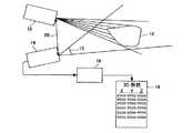
1つの一般的な技法は、既知のパターンの光源で遠隔の物体を照射することであり、それは「構造化照射」と呼ばれる。カメラは、構造化光源から離れたある距離に配置され、遠隔の物体の表面への構造化光パターンを投影した画像を取り込むように配置される。図1は、構造化照射を用いる既知の形状測定を示す。
【0004】
構造化光源10が光を物体12上に投影し、反射された光が、物体12をカバーする視野15を有するカメラ14によって取込まれる。画像プロセッサ16が、構造化光パターンの変形を解析することにより、遠隔の物体への距離を表す3D形状データ18を導出する。
【0005】
遠隔の物体の3D特性によって、カメラによって取り込まれる画像の構造化光パターンが変形する。光源からカメラが物理的にどのくらい離れているか(基線20)を知り、三角法を用いることにより、構造化光パターンの画像の変形から、遠隔の物体の3D表面形状を計算することができる。
【0006】
このシステムの利点は、画像を取り込むためにビデオカメラを用いる場合には、十分に処理することにより、ビデオフレームレート(50あるいは60回/秒)で3D表面形状を測定することができることである。このシステムは、三角法の原理に基づいて動作するので、深さの精度は、システムの基線およびセンサの分解能に関係する。結果として、実用的に検討してみると、数メートルしか離れていない遠隔の物体にそのようなシステムを適用することは制限される傾向がある。さらに、基線が長くなるので、入射光パターンとカメラの視線との間の角度がさらに鋭角になり、遠隔の物体内の特徴によって投じられる影が3D形状測定を覆い隠す可能性がある。
【0007】
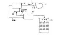
別の技法は、リモートコントロールされたパンおよびチルトユニットを用いて、レーザ距離計(LRF)あるいは干渉計などの、遠隔の点までの距離を測定する装置の走査に頼る。そのようなシステムの一例を図2に示す。
【0008】
レーザ距離計30のような距離測定装置が、物体のある一点までの距離を測定し、パンおよび傾斜ユニット32によって制御される。コンピュータによって制御される制御電子回路34によって、パンおよび傾斜ユニット32は、測定されることになる物体に対して距離測定装置30の視線を走査し、遠隔の物体に対する方位角、仰角および距離の3Dマトリクスを構成できる。この数字のマトリクスは、パンおよび傾斜ユニットの回転軸から極座標で測定される遠隔の物体の3D表面形状を表す。パンおよび傾斜ユニットの回転軸が測定装置の視線と一致しない場合には、そのデータに対してある補正を適用する。結果として生成される3D表面形状18は、既知の数学的技法を用いて、他の座標系に変換できる。その技法は、レーダシステムに類似しており、レーダシステムでは、走査されたマイクロ波無線信号の移動時間を用いて、1つあるいは複数の遠隔の物体までの距離を測定する。
【0009】
この走査式LRFによる手法は、構造化光による手法の範囲限界の影響を受けないが、精度を上げるためには高精度でコストの高い部品を必要とするので、実施するのに比較的コストがかかる。さらに、距離測定装置の全体を走査するので、「リアルタイム」3D画像データを与えるだけの十分な速度で走査を行うには問題がある。
【0010】
この問題点を克服するために、LRFの前に走査式の1つあるいは複数のミラーを用いるシステムが構築されている。たとえば、PCT/US97/06793は、2つの直交するミラーを用いて、約40°×40°の視野を網羅するように水平方向および垂直方向にLRFビームを走査する複雑なシステムを記載する。この手法によって、LRFは、静止した状態でいることができる。しかしながら、1つあるいは複数のミラーは、放射されるレーザビームと受光されるビームとの間にけられや光学的なクロストークを生じることなく、レーザビームと受光システムのレンズ口径とを両方とも網羅するほど十分に大きくなければならないので、そのようなミラー走査式システムは依然としてコストが高い。
【発明の開示】
【発明が解決しようとする課題】
【0011】
距離測定装置が一方向においてラインに沿って走査されると共に、遠隔の物体を回転させるハイブリッド手法が、遠隔の物体の表面全体の3Dマップを作成するために用いられている。しかしながら、これらの技法は、全ての目標物の場合に適切ではない。
【0012】
他の作業者は、GB2 286 495に記載されているように、検出器を静止させたままレーザビームを走査することによりこれらの問題を克服しようとしている。この手法の場合、このシステムの唯一の可動部品は、レーザビームを誘導するために十分に大きいことのみが必要とされる走査式ミラーである。これは、正確にモータによって駆動されるパンおよび傾斜ヘッドにかかる高いコストを避け、速い走査速度を可能にする。さらに、レーザおよび受光用の光路を完全に分離したままにすることができるので、光学的なクロストークが生じる危険性がない。しかしながら、この手法では、受光用の光学系の視野が遠隔の物体全体を網羅する必要がある。結果として、光学系は、視野全体からの照射を取り込むであろう。これは、光学系の光検出器にバックグラウンドオフセット信号レベルを生成する。このオフセットレベルは、信号検出プロセスにおいて補償できるが、オフセット信号レベルに内在するショット雑音が、検出されるレーザ信号レベル対雑音比を著しく劣化させ、それゆえシステムの最大範囲を低減する。
【0013】
この大きな短所を克服するために、非常に複雑な方式が提案されている。その1つが、米国特許第5,682,229号に記載されるようなものであり、走査用レーザからの反射光が固定検出器アセンブリに集束される。固定検出器アセンブリは、一連の複合ファイババンドルを用いて、集束された光を128個の個別のアバランシェフォトダイオードと、関連する移動時間測定回路とに転送する。構成が複雑であり、コヒーレント光ファイバアセンブリおよび多数のディスクリートアバランシェフォトダイオードのような比較的コストが高い部品の使用が、そのようなアプローチの実施を高額にしていると考えられる。
【課題を解決するための手段】
【0014】
本発明によれば、光源と、被測定物体に対して光源からの光を走査するための走査手段と、被測定物体から反射される光を受光するための固定の受光光学系と、受光光学系から入力される光を検出するための多領域光検出器であって、被測定物体の複数の領域が受光光学系によって検出器の複数の領域に投影され、光検出器の複数の領域は個別に動作することができる、多領域光検出器と、光源の走査および光検出器の動作を同期させて光源によって照射されている物体の領域を投影する検出器の領域を動作させるための制御手段と、光源から検出器の動作部までの光信号の移動時間を全ての走査方向について測定するための処理手段とを備えるイメージングシステムが提供される。
【0015】
走査の方向および関連して測定される移動時間を用いて、物体の3次元画像を形成することができる。本発明の装置は、ほとんど可動部品のない簡単な構造を提供する。
【0016】
走査手段は、光源から被測定物体まで光を誘導するための反射器と、反射器の動きを制御して被測定物体に対して光源からの光を走査する駆動機構とを備える。
【0017】
本発明の第2の態様によれば、被測定物体に向けて設けられた光源と、被測定物体から反射される光を受光するための固定の受光光学系と、受光光学系から入力される光を検出するための多領域光検出器と、光源の動作と光検出器の動作とを同期させて、検出器の1つの領域が光源の割り当てられた動作と同期して動作させるための制御手段と、光源から検出器の動作部までの光信号の移動時間を測定するための処理手段とを備えるイメージングシステムが提供される。
【0018】
この態様によれば、多領域光検出器を用いて、可動部品を用いることなくイメージングシステムを構成できる。光検出器の全ての領域が、高速で画像を捉えるために並行に動作できる。しかしながら、光検出器の複数の領域は、個別に動作することが好ましい。これにより、光検出器の複数のサブ領域が順に動作できるようになり、光源の異なる動作が、各サブ領域に割り当てられる。たとえば、各サブ領域は、画素アレイの検出画素の1つの行あるいは列を含むことがある。
【0019】
本発明の第3の態様によれば、各々が被測定物体に向けて設けられている複数の光源と、 被測定物体から反射される光を受光するための固定の受光光学系と、該受光光学系から入力される光を検出するための多領域光検出器であって、各光源は、光検出器の複数の領域に受光光学系によって投影され光検出器の複数の領域は個別に動作できる、多領域光検出器と、光源の各々の動作と光検出器の動作とを同期させて、動作している光源によって照射されている物体の領域を投影する検出器の領域を動作させるための制御手段と、動作している光源から検出器の動作部までの光信号の移動時間を全ての走査方向について測定するための処理手段とを備えるイメージングシステムが提供される。
【0020】
この態様によれば、被検出物体に対して光源出力を走査する必要がなくなる。
【0021】
これらの各態様では、各光源は、パルスレーザあるいは1つまたは複数の発光ダイオードを含むことができる。その出力は、移動時間を測定するために用いられる相互相関法により変調される。
【0022】
本発明のこれらの各態様では、光検出器は、低コストで実施できるフォトダイオードアレイを含むことが好ましい。フォトダイオードアレイは、2つのモードにおいて動作できる。すなわち、第1のモードでは、アレイ内の全てのフォトダイオードからの光信号が順に読み出される。第2のモードでは、アレイ内のフォトダイオードのうちの選択されたフォトダイオードあるいはサブグループからの光信号が順に読み出される。
【0023】
本発明は、物体の画像を取得する方法であって、複数の走査方向に光源出力を順に誘導することにより物体に対して光源信号を走査し、2次元の光検出器アレイを用いて物体から反射されて入力される光を検出する行程と、走査方向毎に照射される光検出器アレイの領域を確定する行程と、物体に対して光源信号を再び走査し、光検出器アレイの確定された領域のみを用いて物体から反射されて受光される光を検出する行程と、走査方向毎に光源から検出器までの光パルスの移動時間を計算する行程と、移動時間の計算から3D形状を得る行程とを含む物体の画像を取得する方法も提供する。
【発明を実施するための最良の形態】
【0024】
ここで、本発明の実施の形態を、添付図面を参照しながら詳細に説明する。
【0025】
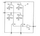
本発明は、固定の受光光学系を備える3Dイメージングシステムを提供する。本発明は、2次元検出器を使用する。2次元検出器を最初に図3を参照しながら説明する。
【0026】
図3に、本発明のイメージングシステムにて使用する2×2の構成のフォトダイオードアレイの概略図を示す。装置は、フォトダイオード画素のアレイ60からなる。各フォトダイオード画素は、フォトダイオード(PD11〜PD22)と、関連するトランジスタ(TR11〜TR22)とを含む。トランジスタ(TR11〜TR22)は、アナログスイッチとして機能するように構成され駆動される。標準的なビデオイメージングの用途の場合、装置は、入射光が表面に集光される積分モードで動作する。入射光は、光電効果によって各フォトダイオードに電荷を生成する。この積分期間中に、ノードX1、X2、Y1、Y2は、全てローに保持されているので、全てのトランジスタがオフであり、フォトダイオードは、電気的に絶縁されている。次に、光によって生成された電荷は、各フォトダイオードに蓄積され、フォトダイオードの内部静電容量に保存される。
【0027】
十分な光電荷が取り込まれると、装置は、以下のように読み出す。入力X1がハイ電位に移行するので、TR1をオンとし、故に、電荷が列と電荷感応増幅器62との間に流れるようになる。次に、画素の行をアドレスするために、入力Y1にハイのパルスが印加され、TR11をオンにし、それにより、光によって生成されてフォトダイオードPD11に保存された電荷が、TR11およびTR1を通って出力増幅器62に流れるようになる。出力増幅器62において、電荷は、電圧に変換される。これにより、振幅がPD11に保存された電荷のレベルに比例し、従ってTR11に入射する光のレベルに比例する出力信号が生成される。
【0028】
PD11の内部静電容量が放電した後、入力Y1は、ローに移行し、入力Y2がハイに移行して、PD12に保存された電荷が読み出される。このようにして、画素の列が次々に読み出される。
【0029】
PD12によって収集された全ての電荷が放電した後に、Y2はローに移行し、X2がハイに移行して、PD21およびPD22(次の列の画素)が、上記のようにY1およびY2にパルスを印加することにより順に読み出される。
【0030】
このプロセスによって、2×2アレイが走査され、入射光に相当する電気信号が生成されることが分かる。通常の動作では、たとえば256×256個のより多くの数のフォトダイオードが、解像度を上げるために使用される。読出しシーケンスおよびセンサ走査は、標準ビデオ信号を生成するように構成されることが多い。
【0031】
なお、実施の形態に記載する基本的な構造は、提案された本発明を説明する目的を果たすために簡略化されている。実用的なX−Yアドレス方式のフォトダイオードアレイは、一般的に、単一の相補型金属酸化膜半導体(CMOS)の大規模集積回路(LSI)として製造される。この集積回路は、電極X1〜XnおよびY1〜Yn用のパルスシーケンスを生成するオンチップクロック回路のような多数の改良を含む。オンチップおよび追加の画素や列レベル回路は、光電荷の増幅および検出を改善する。これらの既知の改良は、本発明に記載される3D形状測定原理に有利に適用される。
【0032】
3D形状測定の場合、本発明者は、かかるX−Yアドレス方式フォトダイオードアレイが、積分モードではなく、レーザ走査およびパルス印加と同期するマルチプレクサとして使用でき、故に、遠隔の物体のレーザスポットの反射画像を受光する個別のフォトダイオードのみにアドレスされることを理解している。
【0033】
図4は、この同期動作モードにおいてフォトダイオードアレイを用いるシステムを示す。レーザ40から次々にパルスとして出力されるレーザビームは、遠隔の物体12の表面の一点を照射する既知の手段によって走査される。サイズおよびコストを低減するために、レーザ走査システム44は、電磁的にあるいは圧電的に走査されるミラー42を使用したり、あるいは微細加工されたシリコンあるいはコンパクトな圧電構造体にレーザチップを実装することを含む、多数の方法で実現される。
【0034】
レーザスポットの画像が、固定された受光光学系46によって、X−Yアドレス方式のフォトダイオードアレイ70の表面に形成される。狭帯域のバンドパス光学フィルタ50を用いて、レーザ波長付近の波長以外の全ての波長を排除し、バックグラウンド照射に対するレーザパルスの識別を最適化する。
【0035】
制御電子回路が、X−Yアドレス方式アレイの関連するXおよびY制御ラインに論理レベル信号を印加し、故に、レーザスポットの画像によって照射されるフォトダイオードが前置増幅器および移動時間検出電子回路56に接続される。詳細には、反射されたレーザパルスは、このフォトダイオードによって取り込まれ、結果として生成された電気信号は、電気パルス検出器54およびTOF(移動時間)測定回路56に送られる。これは、遠隔の物体でのスポットからX−Yアドレス方式アレイのフォトダイオードに戻るまでのレーザパルスのTOFを計算し、それゆえ遠隔の物体からX−Yアドレス方式アレイまでの距離を計算する。次に、このプロセスは、遠隔の物体の表面にわたって多数の点に対して繰り返され、遠隔の物体の表面形状を測定する。レーザスポットから形成される画像が、単一の画素よりも大きい場合には、制御電子回路によって、検出器は、一群の隣接フォトダイオード(たとえば、フォトダイオードの2×2のサブアレイ)に並行してアドレスし、レーザエネルギーの収集および検出を最適化する。
【0036】
いずれの時点においても、受信用増幅器および移動時間電子回路に唯一あるいは少数のフォトダイオードが接続されているので、バックグラウンドオフセット信号は、上記のシステムについては光学系の視野全体からよりは、個々のフォトダイオード/フォトダイオード群に集束される視野の一部によって生成される信号に制限されることが分かる。
【0037】
たとえば、レーザビームが光学視野の100×100の等間隔の点を順に走査するように構成されている場合、各フォトダイオード/フォトダイオード群によって取り込まれるバックグラウンド信号レベルは、上記の簡単なシステムと比較して、見かけ上10,000分の1に低減されることになり、システム性能に大きな利点を与える。
【0038】
なお、このシステムの簡略化された形態は、3D表面形状よりは、2Dを測定する線形フォトダイオードアレイとともに使用できる。
【0039】
システムの性能は、パルスレーザ光源40の代わりに、相互相関システムによる変調レーザ光源およびパルス識別器56を用いることにより、大きく改善される。そのようなシステムは、たとえば、Denso CorpのDE19949803およびPCT/GB/04968から公知である。詳細には、システムは、変調信号を供給するレーザなどの信号源と、変調信号によって変調される被送信光信号を送信する信号源に接続された送信システムとを含むことができる。
【0040】
変調信号は、たとえば最大長シーケンスである。次に、受信システムが、送信信号の反射されて遅延された信号を受信するために設けられ、相互相関器が、時間遅延を得るために設けられる。相互相関器は、粗い分解能で、時間遅延変調信号と受信信号との間の相関を最大にするために必要とされる変調信号の時間遅延を測定するように構成される。次に、相互相関器は、粗い分解能よりも細かい分解能で、測定された時間遅延の周囲のさらに狭い時間遅延範囲内で、受信信号に対する変調信号の時間遅延の関数として、変調信号と受信信号との間の相関を測定できる。距離の測定は、時間遅延された変調信号と受信信号との間の相関を最大にするために必要とされる変調信号の時間遅延から計算される。
【0041】
相互相関器は、デジタル方式で動作される。このようにして、あるレーザピークパワーに対し、次に、より多くのエネルギーが、遠隔の物体に送られ、これにより、信号対雑音比が改善され、それゆえシステムの最大範囲が改善される。このオーバサンプリング手法によって、システムの距離分解能が改善され、粗相互相関器および微細相互相関器を用いる効率的な信号処理方法によって、必要とされる処理能力が低減される。
【0042】
好ましい実施の形態では、X−Yセンサ、移動時間測定システムおよび制御電子回路は、製造コストを抑えるために単一の集積回路上に製造される。フォトダイオードは、アバランシェフォトダイオードとして製造され、動作し、信号検出の前に、アバランシェ効果によって信号増幅を行う。用いられる移動時間測定手法は、図4に関連して先に記載したようであったり、あるいは上記のより高性能の他の機構である。
【0043】
本発明に記載されるようなX−Yセンサは、以下の理由により生じる画像遅延の影響を受ける可能性がある。
a) 1つの画素に入射する光によって生成された光電荷が、フォトダイオードに内在する静電容量と行および列電極の静電容量との間で分割され、結果として、各画素が読み出された後に、行および列電極静電容量に電荷が残ることがある。
b) 負荷抵抗が、フォトダイオード静電容量を放電し、増幅器にバイアスをかけるために設けられる場合があるが、この負荷抵抗の実効抵抗は、増加し、低い光レベルでシステムの時定数を増加させる電流を減少させる。
【0044】
好ましい実施の形態では、この効果は、フォトダイオードアレイがマルチプレクサモードにおいて用いられるとともに、受信用増幅器をトランスインピーダンス増幅器として構成することにより、抑制される。トランスインピーダンス増幅器の入力によって提供される仮想的なアースは、低インピーダンスパスを形成し、そのパスを通って、光によって生成された電流が流れることができ、電荷分割作用を低減し、システム帯域幅を改善する。この手法は、読出し中にフォトダイオードにバイアスをかけるための手段も提供する。好ましい実施の形態の最適な発展形態では、1つのトランスインピーダンス増幅器段が、アレイの多重化回路を駆動するために各画素に設けられる。
【0045】
レーザ走査パターンは、多くの場合に、視野内を移動する物体の位置を測定するために十分な時間分解能を与えながら、光学視野をカバーするように配列される繰返しパターンになる。そのパターンは、通常は、従来のモニタへの表示を容易にするための従来のラスター走査として構成される。しかしながら、他のパターンを用いることもできる。1つの有用なパターンは、螺旋走査パターンであり、レーザ走査の速度を制御することにより、高められた空間分解能が、走査の周辺に現れる物体を検出するために依然として低い空間分解能を保持しながら、走査の中心において達成される。
【0046】
視野内でいくつかの特定の物体の3次元の動作をモニタする必要がある用途の場合、走査は、物体を追跡し、残りの視野を無視するように適応制御される。この手法は、追跡される物体のための時間分解能を高めることができる。
【0047】
記載された手法の重要な利点は、X−Yアドレス方式アレイが、多重化された移動時間検出モードではなく、イメージングモードで動作できることである。これは、単に、X−Yアドレス方式アレイに適用されるパルスのシーケンスを従来のビデオ走査シーケンスに戻すことにより達成できる。
【0048】
これはいくつかの大きな利点を有する。第1に、最適な性能を得る場合に、任意の時点でレーザスポットの画像を受信するフォトダイオードあるいはフォトダイオードの局部的なグループのみがアドレスされること、すなわちレーザ走査とフォトダイオードアレイ走査とが同期していることが重要である。これは、通常、スキャナおよび光学系の正確な較正を必要とする。しかしながら、センサがイメージングモードにありながらレーザが走査される場合、レーザ経路の画像が制御電子回路によって収集される。この画像を用いて、フォトダイオードアレイの表面のレーザビーム画像の正確な経路を測定でき、それゆえ、X−Yアドレス方式アレイのための正確なアドレスシーケンスおよび/またはレーザパルスシーケンスを設定し、多重化された移動時間検出モードにおける同期を保証する。したがって、通常のアドレス指定モードが、より高性能の多重化モードのための較正ステージとして用いられる。実際には、システムは、自動較正され、広い温度範囲にわたって動作しなければならないシステムに対して大きな利点となる。
【0049】
第2に、レーザがオフされ、X−Yアドレス方式フォトダイオードアレイがイメージングモードで動作する場合には、システムは、従来のイメージング装置として、すなわちビデオカメラあるいはスチルカメラとして用いられ、遠隔の物体に関するさらに多くの情報を提供する。
【0050】
第3に、同じ検出器を用いて、3D表面形状と基準画像とが収集されるので、基準画像と3Dデータとの間の重ね合わせが概ね完全である。
【0051】
これにより、従来のイメージングモードと3D形状測定モードとを有利に組み合わせて用いることができるようになる。たとえば、3D走査を収集することと、従来の画像走査との間でシステムを切り替えることにより、ビデオ画像シーケンスと3Dシーケンスとの両方が収集され、互いに重ね合わせられる。この手法は、衝突回避あるいは侵入者検出の場合に特に有利である。3D画像が、視野内の物体が接近しすぎているか、あるいは衝突に至る可能性がある経路上にあることを示す場合には、その問題に注意を引き付けるために、従来の画像の対応する部分が着色されたり、あるいは閃光するようになされることができる。
【0052】
完全に重ね合わされた3Dおよび従来の画像データを収集する別の利点は、画像処理方法が両方のデータの組に同時に適用され、最適な方法を用いて各画像から重要な特徴を抽出し、特徴データを組み合わせて、視野内の物体についてさらに多くの情報を生成できることである。たとえば、3Dデータを用いて、視野内の物体の向きおよびサイズを判別することができる。次に、このデータを用いて、パターンマッチングおよび物体/対象物認識のための適当なパターンを、あるいは既知の物体の3Dソリッドモデルから選択したり生成することができる。
【0053】
完全に重ね合わされた3Dおよび従来の画像データを収集する利点が数多くあることが分かる。
【0054】
より高速の走査速度が必要とされる場合、上記のシステムは、遠隔の物体の点ではなく線を照射するようにレーザの光学系を変更し、さらに、フォトダイオードの行が多数の移動時間測定プロセッサに並列に接続されるようにX−Yアドレス方式アレイの構造を変更することにより、すなわちY走査X並列出力アレイによって改善することができる。
【0055】
修正されたフォトダイオードアレイ構造の1つの実施の形態を2×2アレイ用に図5に示す。各列スイッチトランジスタが、増幅器80と、パルス検出器82、カウンタ84およびラッチ86を含む移動時間測定(TOF)回路とによって置き換えられている。
【0056】
全てのカウンタ84が、共通のクロック入力88によって同じ周波数でクロックされる。レーザ走査システムは、遠隔の物体の帯を照射するように設定される。照射された帯の画像は、フォトダイオードアレイの行N上に集光される。レーザがパルス化され、TOFカウンタ84が0にリセットされ、制御電子回路が関連するY電極(Y1、Y2)をハイに移行し、その行に沿った全てのフォトダイオードを対応する増幅器およびTOF回路に接続する。各フォトダイオードがレーザ光の反射されたパルスを受光するので、パルス検出器によって、対応するカウンタ84がカウントを中止する。全ての反射パルスが受光されると、各カウンタ84に保持された数がラッチ86にラッチされ、通常の方法で読み出され、一方、次の行が照射され、そのプロセスが繰り返される。各ラッチ内に保存される数は、移動時間に比例し、それにより、レーザ線によって照射されフォトダイオードによって投影された点の各々までの距離が測定できる。
【0057】
性能を改善するために、移動時間測定回路は、上記の同じ原理を使用できる。
【0058】
この手法では、視差効果を光学系に近い物体に対しては考慮しなければならない。これらの効果は、レーザ源および受光光学系をできる限り接近させて構成したり、あるいは好ましくは同時にビームスプリッタを使用することによって低減される。あるいは、レーザ線で遠隔の物体の幅広い帯を照射して、フォトダイオードの1つの行が全て反射光を確実に受光するように焦点をぼかすことができる。別の手法は、制御電子回路によって、各列内の1つのフォトダイオードではなく、複数のフォトダイオードを同時に列増幅器に接続することである。この技法は、単独で、あるいは組み合わせて用いることができる。
【0059】
あらゆる可動部品の必要性を不要にすることにより、多数のパルスまたは変調光源を含む照射システムを用いることができる。この手法を図6に示す。図6において、3つのレーザダイオード90A、90B、90Cを含み、各レーザーダイオードが受光光学系の視野92の領域91A、91B、91Cを照射するように構成されている照射システムを示す。各光源は、照射する領域がY走査X並列出力アレイの読出しと同期できるように順に動作される。光源、たとえばレーザダイオードあるいは発光ダイオード(LED)は、コストを低減するために、駆動回路が集積された共通の基板に製造されることが好ましい。個々の光源の出力を誘導して集光するために、各々が個々の光源と直線的に配列されるマイクロレンズアレイを製造することが有利である。
【0060】
最終的な用途の要件によって、多数の様々なレーザ/マルチプレクサの組み合わせを用いることができる。
【0061】
たとえば、1つの線に沿って距離形状を測定することのみが必要とされる場合には、フォトダイオードの1次元のアレイを用いることができる。当該分野の当業者には、1つの線に沿って距離形状を測定するための検出器アレイとして電荷結合素子(CCD)を使用できることは理解されよう。これは、変調光源の場合に特に適切である。この場合には、2次元のCCDアレイが、並列な読出しレジスタから最も離れた、画像セクション画素の最上位の行が照射されるようにマスクされる。次に、CCD画像セクションが、光源の変調と同期して時間遅延および積分(TDI)モードにおいてクロックされ、同時に照射された行内の画素毎に反射された変調シーケンスを取り込む。次に、取り込まれたシーケンスが通常の方法でCCDから読み出され、相互相関を用いて各列からのデータが処理され、光源から各列の最上位の照射画素までの移動時間を抽出する。
【0062】
また、簡単なシステムは、単一の明るいパルス化光源あるいは変調光源を用いて同時に視野全体と、上記の方法で3D画像データを収集するために使用されるX−Yアドレス方式アレイ、すなわちY走査X並列出力アレイとを照射することで実現する。
【0063】
これにより、イメージングシステムは、可動部品を用いることなく構成できる。光源は、同時に読み出される検出器アレイの画素の1グループ当たり一度だけ動作する。超高速の用途の場合、TOF測定回路は、アレイ内のフォトダイオード毎に設けられる。したがって、画素のグループは、画素の全アレイになる。これにより、TOF、それゆえ遠隔の物体までの距離が、視野内の全ての点に対して並行して測定される。
【0064】
しかしながら、より低コストの実施では、光検出器の複数の領域が次々に個別に動作される。シーケンスは、行および列ドライバ回路の構成に応じて、行毎あるいは列毎になる。これにより、光検出器の異なるサブ領域(行あるいは列)が順に動作するようになり、光源の複数の領域が各サブ領域に割り当てられる。
【0065】
上記の全ての実施の形態では、検出器画素アレイの距離測定動作モードは、直接読出し動作モードを含む。このモードにおいて、光によって生成された電荷は、測定回路に直接に移動し、その結果、入射光の到着時刻がわかる。イメージングモードは、積分動作モードである。このモードにおいて、電荷は、フォトダイオードの内部静電容量(あるいは画素レイアウト内の付加電荷蓄積容量)に蓄積できる。行および列ドライバ回路は、これら2つの異なるモードにおいて動作できる必要があり、これは、通常は、2つのモードにおいて異なる制御電圧およびタイミングを必要とする。
【0066】
実現可能な特定の画素構成および制御方式は、当業者には明らかである。
【図面の簡単な説明】
【0067】
【図1】第1の既知の3Dイメージングシステムを示す図である。
【図2】第2の既知の3Dイメージングシステムを示す図である。
【図3】本発明のシステムにおいて使用されるフォトダイオードアレイの簡略化された例を示す図である。
【図4】図3のフォトダイオードアレイを用いる本発明のイメージングシステムを示す図である。
【図5】フォトダイオードアレイの変更例を示す図である。
【図6】本発明のイメージングシステムにおけるパルス光源の使用方法を示す図である。
【符号の説明】
【0068】
40 光源
44 走査手段
46 受光光学系
52 制御手段
56 処理手段
70 多領域光検出器【Technical field】
[0001]
The present invention relates to an apparatus for measuring a surface shape of a sample, and in particular, to a non-contact 3D surface shape measurement system.
[Background Art]
[0002]
Measuring a three-dimensional (3D) object in a non-contact manner and extracting data relating to the physical shape and position of the object in space have been actively studied. Numerous techniques have been developed to suit the distance to the object and the accuracy required to measure the characteristics of the object.
[0003]
One common technique is to illuminate a remote object with a known pattern of light sources, which is called "structured illumination." A camera is positioned at a distance from the structured light source and is positioned to capture an image that projects the structured light pattern onto the surface of a remote object. FIG. 1 shows a known shape measurement using structured irradiation.
[0004]
[0005]
The 3D characteristics of the distant object alter the structured light pattern of the image captured by the camera. Knowing how far the camera is physically away from the light source (baseline 20) and using trigonometry, the 3D surface shape of the remote object can be calculated from the deformation of the image of the structured light pattern.
[0006]
The advantage of this system is that if a video camera is used to capture the image, it can be well processed to measure the 3D surface profile at the video frame rate (50 or 60 times / second). Since this system operates on the principle of trigonometry, the accuracy of the depth is related to the baseline of the system and the resolution of the sensor. As a result, practical considerations tend to limit the application of such systems to remote objects that are only a few meters away. Further, as the baseline becomes longer, the angle between the incident light pattern and the line of sight of the camera becomes even sharper, and shadows cast by features in distant objects can obscure 3D shape measurements.
[0007]
Another technique relies on the scanning of a device that measures the distance to a remote point, such as a laser range finder (LRF) or interferometer, using a remotely controlled pan and tilt unit. One example of such a system is shown in FIG.
[0008]
A distance measuring device such as a laser range finder 30 measures the distance to a point on the object and is controlled by a pan and
[0009]
Although the scanning LRF method is not affected by the range limit of the structured light method, it requires relatively high-precision and high-cost parts in order to increase accuracy, so that it is relatively costly to implement. Take it. In addition, since the entire distance measurement device is scanned, it is problematic to scan at a sufficient speed to provide "real-time" 3D image data.
[0010]
To overcome this problem, systems have been built that use one or more scanning mirrors before the LRF. For example, PCT / US97 / 06793 describes a complex system that uses two orthogonal mirrors to scan an LRF beam horizontally and vertically to cover an approximately 40 ° × 40 ° field of view. This approach allows the LRF to remain stationary. However, one or more mirrors can cover both the laser beam and the lens diameter of the light receiving system without causing eclipse or optical crosstalk between the emitted laser beam and the received beam. Such mirror scanning systems are still costly because they must be large enough to operate.
DISCLOSURE OF THE INVENTION
[Problems to be solved by the invention]
[0011]
A hybrid approach in which the distance measurement device is scanned along a line in one direction and the remote object is rotated has been used to create a 3D map of the entire surface of the remote object. However, these techniques are not appropriate for all targets.
[0012]
Other workers have attempted to overcome these problems by scanning the laser beam with the detector stationary, as described in GB2 286 495. With this approach, the only moving parts of the system are scanning mirrors, which need only be large enough to direct the laser beam. This avoids the high cost of pan and tilt heads that are precisely driven by the motor and allows for fast scanning speeds. Furthermore, since the laser and the receiving optical path can be kept completely separate, there is no danger of optical crosstalk. However, in this method, the field of view of the light receiving optical system needs to cover the entire remote object. As a result, the optics will capture illumination from the entire field of view. This creates a background offset signal level at the optical detector of the optical system. This offset level can be compensated for in the signal detection process, but the shot noise inherent in the offset signal level significantly degrades the detected laser signal level-to-noise ratio, thus reducing the maximum range of the system.
[0013]
To overcome this major disadvantage, very complex schemes have been proposed. One is as described in U.S. Pat. No. 5,682,229, in which reflected light from a scanning laser is focused on a fixed detector assembly. The fixed detector assembly uses a series of composite fiber bundles to transfer the focused light to the 128 individual avalanche photodiodes and associated travel time measurement circuitry. The complexity of the construction and the use of relatively costly components such as coherent fiber optic assemblies and numerous discrete avalanche photodiodes are thought to make the implementation of such approaches expensive.
[Means for Solving the Problems]
[0014]
According to the present invention, a light source, scanning means for scanning a light from a light source with respect to a measured object, a fixed light receiving optical system for receiving light reflected from the measured object, and a light receiving optical system A multi-area photodetector for detecting light input from the system, wherein a plurality of areas of the measured object are projected onto a plurality of areas of the detector by a light receiving optical system, and a plurality of areas of the photodetector are A multi-region photodetector, which can be operated independently, and a control for operating a region of the detector that projects the region of the object illuminated by the light source by synchronizing the scanning of the light source and the operation of the light detector. An imaging system is provided comprising means and processing means for measuring the transit time of the optical signal from the light source to the working part of the detector for all scanning directions.
[0015]
A three-dimensional image of the object can be formed using the direction of the scan and the associated measured transit time. The device of the present invention provides a simple structure with few moving parts.
[0016]
The scanning means includes a reflector for guiding light from the light source to the object to be measured, and a drive mechanism for controlling movement of the reflector to scan the object to be measured with light from the light source.
[0017]
According to the second aspect of the present invention, a light source provided to an object to be measured, a fixed light receiving optical system for receiving light reflected from the object to be measured, and an input from the light receiving optical system A multi-region photodetector for detecting light, a control for synchronizing the operation of the light source and the operation of the light detector, and operating one region of the detector in synchronization with the assigned operation of the light source An imaging system is provided comprising means and processing means for measuring the transit time of an optical signal from a light source to a working part of a detector.
[0018]
According to this aspect, an imaging system can be configured using a multi-area photodetector without using a movable part. All regions of the photodetector can operate in parallel to capture images at high speed. However, the regions of the photodetector preferably operate individually. This allows the plurality of sub-regions of the photodetector to operate sequentially, with different operations of the light source being assigned to each sub-region. For example, each sub-region may include one row or column of detected pixels of a pixel array.
[0019]
According to a third aspect of the present invention, a plurality of light sources each provided toward an object to be measured, a fixed light receiving optical system for receiving light reflected from the object to be measured, A multi-area photodetector for detecting light input from an optical system, wherein each light source is projected by a light receiving optical system onto a plurality of areas of the photodetector, and the plurality of areas of the photodetector operate individually. Possible to synchronize the operation of each of the light source and the operation of the light detector with the multi-region light detector, to operate the region of the detector which projects the region of the object illuminated by the operating light source And a processing means for measuring the travel time of the optical signal from the operating light source to the operating part of the detector in all the scanning directions.
[0020]
According to this aspect, there is no need to scan the light source output with respect to the detected object.
[0021]
In each of these aspects, each light source may include a pulsed laser or one or more light emitting diodes. Its output is modulated by the cross-correlation method used to measure travel time.
[0022]
In each of these aspects of the invention, the photodetector preferably includes a photodiode array that can be implemented at low cost. The photodiode array can operate in two modes. That is, in the first mode, optical signals from all the photodiodes in the array are sequentially read. In the second mode, optical signals from selected photodiodes or subgroups of the photodiodes in the array are sequentially read.
[0023]
The present invention is a method for acquiring an image of an object, in which a light source signal is scanned on the object by sequentially guiding light source outputs in a plurality of scanning directions, and the object is scanned from the object using a two-dimensional photodetector array. A step of detecting reflected and input light, a step of determining an area of the photodetector array irradiated in each scanning direction, and a step of re-scanning the object with a light source signal to determine the photodetector array. Detecting light reflected from the object and receiving light using only the detected area, calculating the moving time of the light pulse from the light source to the detector for each scanning direction, and calculating the 3D shape from the calculating of the moving time. There is also provided a method of obtaining an image of an object, comprising:
BEST MODE FOR CARRYING OUT THE INVENTION
[0024]
Here, embodiments of the present invention will be described in detail with reference to the accompanying drawings.
[0025]
The present invention provides a 3D imaging system including a fixed receiving optical system. The present invention uses a two-dimensional detector. The two-dimensional detector will be described first with reference to FIG.
[0026]
FIG. 3 shows a schematic diagram of a photodiode array having a 2 × 2 configuration used in the imaging system of the present invention. The device comprises an
[0027]
When enough photocharge has been captured, the device reads as follows. Since input X1 goes to a high potential, TR1 is turned on, thus allowing charge to flow between the column and charge
[0028]
After the internal capacitance of the PD 11 has been discharged, the input Y1 goes low, the input Y2 goes high, and the charge stored in the
[0029]
After all the charge collected by PD12 has discharged, Y2 goes low and X2 goes high, causing PD21 and PD22 (the next column of pixels) to pulse Y1 and Y2 as described above. It is read out sequentially by applying.
[0030]
It can be seen that this process scans the 2 × 2 array and produces an electrical signal corresponding to the incident light. In normal operation, a larger number of photodiodes, for example 256.times.256, are used to increase the resolution. Readout sequences and sensor scans are often configured to generate standard video signals.
[0031]
It should be noted that the basic structure described in the embodiments has been simplified to fulfill the purpose of describing the proposed invention. A practical XY addressing photodiode array is typically manufactured as a single complementary metal oxide semiconductor (CMOS) large scale integrated circuit (LSI). This integrated circuit includes a number of improvements, such as an on-chip clock circuit that generates a pulse sequence for the electrodes X1-Xn and Y1-Yn. On-chip and additional pixel and column level circuits improve photocharge amplification and detection. These known improvements are advantageously applied to the 3D shape measurement principle described in the present invention.
[0032]
In the case of 3D shape measurement, the inventor has determined that such an XY-addressed photodiode array can be used as a multiplexer that synchronizes with laser scanning and pulsing, rather than in integration mode, thus reflecting the laser spot of a remote object It is understood that only the individual photodiode receiving the image is addressed.
[0033]
FIG. 4 shows a system using a photodiode array in this synchronous operation mode. The laser beam, which is pulsed from the
[0034]
An image of the laser spot is formed on the surface of the XY address
[0035]
The control electronics applies logic level signals to the associated X and Y control lines of the XY addressing array, so that the photodiode illuminated by the image of the laser spot uses a preamplifier and travel
[0036]
At any one time, since only one or a small number of photodiodes are connected to the receiving amplifier and the transit time electronics, the background offset signal is more individual for the above system than for the entire optical field of view. It can be seen that the signal is limited to the signal generated by the part of the field of view focused on the photodiode / photodiode group.
[0037]
For example, if the laser beam is configured to sequentially scan 100 × 100 equally spaced points in the optical field of view, the background signal level captured by each photodiode / photodiode group will be equal to the simple system described above. In comparison, it will be apparently reduced by a factor of 10,000, giving a significant advantage to system performance.
[0038]
It should be noted that the simplified form of this system can be used with linear photodiode arrays that measure 2D rather than 3D topography.
[0039]
The performance of the system is greatly improved by using a
[0040]
The modulation signal is, for example, a maximum length sequence. Next, a receiving system is provided for receiving the reflected delayed signal of the transmitted signal, and a cross-correlator is provided for obtaining the time delay. The cross correlator is configured to measure, with coarse resolution, the time delay of the modulated signal required to maximize the correlation between the time delayed modulated signal and the received signal. The cross-correlator then combines the modulated signal with the received signal as a function of the time delay of the modulated signal with respect to the received signal at a finer resolution than the coarse resolution and within a narrower time delay range around the measured time delay. Can be measured. The distance measurement is calculated from the time delay of the modulated signal required to maximize the correlation between the time delayed modulated signal and the received signal.
[0041]
The cross-correlator is operated digitally. In this way, for a given laser peak power, more energy is then sent to the remote object, which improves the signal-to-noise ratio and therefore the maximum range of the system. This oversampling approach improves the range resolution of the system and reduces the required processing power by efficient signal processing methods using coarse and fine cross-correlators.
[0042]
In a preferred embodiment, the XY sensors, travel time measurement system and control electronics are manufactured on a single integrated circuit to reduce manufacturing costs. Photodiodes are manufactured and operated as avalanche photodiodes and perform signal amplification by the avalanche effect before signal detection. The transit time measurement technique used may be as described above in connection with FIG. 4 or other of the more sophisticated mechanisms described above.
[0043]
An XY sensor as described in the present invention may be subject to image delays caused by the following reasons.
a) Photocharges generated by light incident on one pixel are split between the capacitance inherent in the photodiode and the capacitance of the row and column electrodes, resulting in each pixel being read out After that, charges may remain in the row and column electrode capacitances.
b) A load resistor may be provided to discharge the photodiode capacitance and bias the amplifier, but the effective resistance of this load resistor will increase, increasing the time constant of the system at low light levels To reduce the current.
[0044]
In a preferred embodiment, this effect is suppressed by using the photodiode array in a multiplexer mode and configuring the receiving amplifier as a transimpedance amplifier. The virtual ground provided by the input of the transimpedance amplifier forms a low impedance path through which current generated by light can flow, reducing charge splitting effects and reducing system bandwidth. To improve. This approach also provides a means for biasing the photodiode during readout. In an optimal development of the preferred embodiment, one transimpedance amplifier stage is provided for each pixel to drive the multiplexing circuits of the array.
[0045]
The laser scan pattern is often a repeating pattern arranged to cover the optical field of view, while providing sufficient time resolution to determine the position of an object moving within the field of view. The pattern is typically configured as a conventional raster scan to facilitate display on a conventional monitor. However, other patterns can be used. One useful pattern is a helical scan pattern, where by controlling the speed of the laser scan, the enhanced spatial resolution still retains a low spatial resolution to detect objects appearing around the scan, Achieved at the center of the scan.
[0046]
For applications where it is necessary to monitor the three-dimensional movement of some particular objects in the field of view, the scan is adaptively controlled to track the objects and ignore the remaining fields of view. This approach can increase the temporal resolution for the tracked object.
[0047]
An important advantage of the described approach is that the XY addressable array can operate in an imaging mode rather than a multiplexed transit time detection mode. This can be achieved simply by reverting the sequence of pulses applied to the XY addressed array to a conventional video scan sequence.
[0048]
This has several major advantages. First, for optimal performance, only the photodiodes or local groups of photodiodes that receive the image of the laser spot at any given time are addressed, i.e., laser scanning and photodiode array scanning It is important that they are synchronized. This usually requires accurate calibration of the scanner and optics. However, if the laser is scanned while the sensor is in the imaging mode, images of the laser path are collected by the control electronics. This image can be used to determine the exact path of the laser beam image on the surface of the photodiode array, thus setting the correct address sequence and / or laser pulse sequence for the XY addressable array and multiplexing. Synchronization in the simplified travel time detection mode. Therefore, the normal addressing mode is used as a calibration stage for the higher performance multiplexing mode. In practice, the system is self-calibrating, which is a great advantage over systems that must operate over a wide temperature range.
[0049]
Second, when the laser is turned off and the XY addressing photodiode array operates in an imaging mode, the system can be used as a conventional imaging device, i.e., as a video or still camera, for remote objects. Provides more information.
[0050]
Third, the registration between the reference image and the 3D data is substantially complete, since the 3D surface shape and the reference image are collected using the same detector.
[0051]
Thereby, the conventional imaging mode and 3D shape measurement mode can be advantageously used in combination. For example, by switching the system between acquiring a 3D scan and conventional image scanning, both the video image sequence and the 3D sequence are acquired and superimposed on each other. This technique is particularly advantageous for collision avoidance or intruder detection. If the 3D image indicates that the object in the field of view is too close or on a path that could lead to a collision, the corresponding part of the conventional image is used to draw attention to the problem Can be colored or made to flash.
[0052]
Another advantage of collecting fully superimposed 3D and conventional image data is that the image processing method is applied to both sets of data simultaneously, extracting important features from each image using optimal methods, The ability to combine data to generate more information about objects in the field of view. For example, the orientation and size of the object in the field of view can be determined using the 3D data. This data can then be used to select and generate appropriate patterns for pattern matching and object / object recognition, or from 3D solid models of known objects.
[0053]
It can be seen that there are many advantages to collecting fully superimposed 3D and conventional image data.
[0054]
When higher scan speeds are required, the above system modifies the laser optics to illuminate a line rather than a point on a distant object, and furthermore, the rows of photodiodes have a large number of travel time measurements. This can be improved by modifying the structure of the XY addressing array to be connected in parallel to the processor, i.e., with a Y-scan X parallel output array.
[0055]
One embodiment of a modified photodiode array structure is shown in FIG. 5 for a 2 × 2 array. Each column switch transistor has been replaced by an
[0056]
All counters 84 are clocked at the same frequency by a
[0057]
To improve performance, the travel time measurement circuit can use the same principles described above.
[0058]
In this method, the parallax effect must be considered for an object close to the optical system. These effects are reduced by configuring the laser source and receiving optics as close as possible or, preferably, simultaneously using a beam splitter. Alternatively, a wide band of the remote object can be illuminated with a laser beam and defocused to ensure that one row of photodiodes receives all the reflected light. Another approach is to connect multiple photodiodes to the column amplifier simultaneously, rather than one photodiode in each column, by control electronics. This technique can be used alone or in combination.
[0059]
By eliminating the need for any moving parts, illumination systems that include multiple pulsed or modulated light sources can be used. This technique is illustrated in FIG. FIG. 6 shows an illumination system including three
[0060]
Many different laser / multiplexer combinations can be used, depending on the requirements of the final application.
[0061]
For example, a one-dimensional array of photodiodes can be used if only the distance shape needs to be measured along one line. Those skilled in the art will appreciate that a charge coupled device (CCD) can be used as a detector array for measuring distance profiles along a single line. This is particularly appropriate for modulated light sources. In this case, the two-dimensional CCD array is masked such that the top row of image section pixels furthest from the parallel readout registers is illuminated. Next, the CCD image section is clocked in time delay and integration (TDI) mode in synchronization with the modulation of the light source and simultaneously captures the reflected modulation sequence for each pixel in the illuminated row. The captured sequence is then read from the CCD in the usual manner, and the data from each column is processed using cross-correlation to extract the travel time from the light source to the top illuminated pixel in each column.
[0062]
Also, a simple system is to use a single bright pulsed or modulated light source at the same time and the entire field of view, and an XY-addressed array, or Y-scan, used to acquire 3D image data in the manner described above. This is realized by irradiating an X parallel output array.
[0063]
Thus, the imaging system can be configured without using any moving parts. The light source operates only once per group of pixels of the detector array that are read out simultaneously. For very high speed applications, a TOF measurement circuit is provided for each photodiode in the array. Thus, the group of pixels becomes the entire array of pixels. Thereby, the distance to the TOF and hence the remote object is measured in parallel for all points in the field of view.
[0064]
However, in lower cost implementations, multiple regions of the photodetector are operated individually one after the other. The sequence is row-wise or column-wise, depending on the configuration of the row and column driver circuits. This allows different sub-regions (rows or columns) of the photodetector to operate in order, and a plurality of regions of the light source are assigned to each sub-region.
[0065]
In all the above embodiments, the distance measurement operation mode of the detector pixel array includes the direct readout operation mode. In this mode, the charge generated by the light travels directly to the measurement circuit, so that the arrival time of the incident light is known. The imaging mode is an integration operation mode. In this mode, charge can be stored in the internal capacitance of the photodiode (or additional charge storage capacitance in the pixel layout). The row and column driver circuits need to be able to operate in these two different modes, which typically require different control voltages and timing in the two modes.
[0066]
The specific pixel configurations and control schemes that can be realized will be apparent to those skilled in the art.
[Brief description of the drawings]
[0067]
FIG. 1 shows a first known 3D imaging system.
FIG. 2 shows a second known 3D imaging system.
FIG. 3 shows a simplified example of a photodiode array used in the system of the present invention.
FIG. 4 is a diagram showing an imaging system of the present invention using the photodiode array of FIG. 3;
FIG. 5 is a diagram showing a modified example of a photodiode array.
FIG. 6 is a diagram illustrating a method of using a pulse light source in the imaging system of the present invention.
[Explanation of symbols]
[0068]
40 light source
44 Scanning means
46 Receiving optical system
52 control means
56 processing means
70 Multi-area photodetector
Claims (24)
Translated fromJapanese被測定物体に対して前記光源からの光を走査するための走査手段と、
前記被測定物体から反射される光を受光するための固定の受光光学系と、
前記受光光学系から入力される光を検出するための多領域光検出器であって、前記被測定物体の複数の領域が前記受光光学系によって前記検出器の複数の領域に投影され、前記光検出器の複数の領域は個別に動作することができる、多領域光検出器と、
前記光源の走査および前記光検出器の動作を同期させて前記光源によって照射されている前記物体の領域を投影する前記検出器の領域を動作させるための制御手段と、
前記光源から前記検出器の前記動作部までの光信号の移動時間を全ての走査方向について測定するための処理手段と
を備えるイメージングシステム。A light source,
Scanning means for scanning the object to be measured with light from the light source,
A fixed light receiving optical system for receiving light reflected from the measured object,
A multi-area light detector for detecting light input from the light receiving optical system, wherein a plurality of areas of the measured object are projected onto a plurality of areas of the detector by the light receiving optical system, and the light A multi-region photodetector, wherein the plurality of regions of the detector can operate independently;
Control means for operating the area of the detector that projects the area of the object illuminated by the light source in synchronization with the scanning of the light source and the operation of the light detector,
Processing means for measuring the travel time of the optical signal from the light source to the operating part of the detector in all scanning directions.
前記光源から被測定物体まで前記光を誘導するための反射器と、
前記反射器の動きを制御して前記被測定物体に対して前記光源からの前記光を走査する駆動機構と
を備える先行する請求項のいずれか一項に記載のイメージングシステム。The scanning means,
A reflector for guiding the light from the light source to the measured object,
The imaging system according to any one of the preceding claims, further comprising a driving mechanism configured to control a movement of the reflector to scan the object from the light source with respect to the measured object.
前記被測定物体から反射される光を受光するための固定の受光光学系と、
該受光光学系から入力される光を検出するための多領域光検出器であって、前記各光源は、前記光検出器の複数の領域に前記受光光学系によって投影され前記光検出器の複数の領域は個別に動作できる、多領域光検出器と、
前記光源の各々の動作と前記光検出器の動作とを同期させて、動作している光源によって照射されている前記物体の領域を投影する前記検出器の領域を動作させるための制御手段と、
前記動作している光源から前記検出器の動作部までの光信号の移動時間を全ての走査方向について測定するための処理手段と
を備えるイメージングシステム。A plurality of light sources, each provided towards the object to be measured,
A fixed light receiving optical system for receiving light reflected from the measured object,
A multi-region light detector for detecting light input from the light receiving optical system, wherein each of the light sources is projected by the light receiving optical system onto a plurality of regions of the light detector and a plurality of the light detectors are projected. Regions can operate independently, a multi-region photodetector,
Control means for synchronizing the operation of each of the light sources and the operation of the photodetector, and operating an area of the detector that projects an area of the object illuminated by the operating light source,
Processing means for measuring the travel time of the optical signal from the operating light source to the operating section of the detector in all scanning directions.
前記被測定物体から反射される光を受光するための固定の受光光学系と、
前記受光光学系から入力される光を検出するための多領域光検出器と、
前記光源の動作と前記光検出器の動作とを同期させて、前記検出器の1つの領域が前記光源の割り当てられた動作と同期して動作させるための制御手段と、
前記光源から前記検出器の前記動作部までの光信号の移動時間を測定するための処理手段と
を備えるイメージングシステム。A light source provided toward the object to be measured,
A fixed light receiving optical system for receiving light reflected from the measured object,
A multi-area photodetector for detecting light input from the light receiving optical system,
Control means for synchronizing the operation of the light source with the operation of the photodetector and operating one region of the detector in synchronization with the assigned operation of the light source;
Processing means for measuring a travel time of an optical signal from the light source to the operating part of the detector.
複数の走査方向に光源出力を順に誘導することにより前記物体に対して光源信号を走査し、2次元の光検出器アレイを用いて前記物体から反射されて入力される光を検出する行程と、
前記走査方向毎に照射される前記光検出器アレイの領域を確定する行程と、
前記物体に対して前記光源信号を再び走査し、前記光検出器アレイの前記確定された領域のみを用いて前記物体から反射されて受光される光を検出する行程と、
走査方向毎に前記光源から前記検出器までの光パルスの移動時間を計算する行程と、
前記移動時間の計算から3D形状を得る行程と
を含む物体の画像を取得する方法。A method for obtaining an image of an object, comprising:
Scanning a light source signal with respect to the object by sequentially guiding light source outputs in a plurality of scanning directions, and detecting light reflected and input from the object using a two-dimensional photodetector array,
A step of determining an area of the photodetector array irradiated for each of the scanning directions;
Scanning the light source signal again for the object and detecting light reflected and received from the object using only the determined area of the photodetector array;
Calculating a moving time of a light pulse from the light source to the detector for each scanning direction;
Obtaining a 3D shape from the calculation of the travel time.
Applications Claiming Priority (3)
| Application Number | Priority Date | Filing Date | Title |
|---|---|---|---|
| GB0108497AGB2374743A (en) | 2001-04-04 | 2001-04-04 | Surface profile measurement |
| GB0110577AGB2374228A (en) | 2001-04-04 | 2001-04-30 | A collision warning device |
| PCT/GB2002/001612WO2002082016A1 (en) | 2001-04-04 | 2002-04-04 | Surface profile measurement |
Publications (2)
| Publication Number | Publication Date |
|---|---|
| JP2004523769Atrue JP2004523769A (en) | 2004-08-05 |
| JP4405154B2 JP4405154B2 (en) | 2010-01-27 |
Family
ID=26245931
Family Applications (2)
| Application Number | Title | Priority Date | Filing Date |
|---|---|---|---|
| JP2002580103AExpired - Fee RelatedJP4405155B2 (en) | 2001-04-04 | 2002-04-04 | Image analysis system |
| JP2002579742AExpired - Fee RelatedJP4405154B2 (en) | 2001-04-04 | 2002-04-04 | Imaging system and method for acquiring an image of an object |
Family Applications Before (1)
| Application Number | Title | Priority Date | Filing Date |
|---|---|---|---|
| JP2002580103AExpired - Fee RelatedJP4405155B2 (en) | 2001-04-04 | 2002-04-04 | Image analysis system |
Country Status (8)
| Country | Link |
|---|---|
| US (2) | US7319777B2 (en) |
| EP (2) | EP1373830B1 (en) |
| JP (2) | JP4405155B2 (en) |
| AT (2) | ATE310268T1 (en) |
| DE (2) | DE60207395T2 (en) |
| ES (2) | ES2264476T3 (en) |
| PT (1) | PT1373830E (en) |
| WO (2) | WO2002082016A1 (en) |
Cited By (15)
| Publication number | Priority date | Publication date | Assignee | Title |
|---|---|---|---|---|
| JP2004529343A (en)* | 2001-04-04 | 2004-09-24 | インストロ プレシジョン リミテッド | Image analysis device |
| JP2006242801A (en)* | 2005-03-04 | 2006-09-14 | Mitsui Eng & Shipbuild Co Ltd | 3D image information acquisition device |
| JP2010502947A (en)* | 2006-08-30 | 2010-01-28 | ユーエスエヌアール・コッカムス・キャンカー・カンパニー | Scanner system for charger |
| JP2011133271A (en)* | 2009-12-22 | 2011-07-07 | Panasonic Electric Works Co Ltd | Object detector |
| JP2011160420A (en)* | 2010-02-02 | 2011-08-18 | Primesense Ltd | Synchronization of projected illumination with rolling shutter of image sensor |
| JP2013050310A (en)* | 2011-08-30 | 2013-03-14 | Stanley Electric Co Ltd | Distance image generation device |
| KR101394050B1 (en) | 2012-12-18 | 2014-05-09 | 현대자동차 주식회사 | Method for image recognition using backlight in a vehicle |
| JP2015172551A (en)* | 2014-03-12 | 2015-10-01 | スタンレー電気株式会社 | Distance image generating apparatus and distance image generating method |
| KR101762525B1 (en)* | 2013-03-15 | 2017-07-27 | 애플 인크. | Apparatus and method for depth scanning with multiple emitters |
| CN108139210A (en)* | 2015-05-04 | 2018-06-08 | 株式会社三丰 | Inspection program editing environment providing user-defined collision avoidance volumes |
| WO2018186153A1 (en)* | 2017-04-06 | 2018-10-11 | 京セラ株式会社 | Electromagnetic wave detection device, program, and electromagnetic wave detection system |
| WO2019021887A1 (en)* | 2017-07-27 | 2019-01-31 | シャープ株式会社 | Optical radar device |
| JP2020530109A (en)* | 2017-08-31 | 2020-10-15 | エスゼット ディージェイアイ テクノロジー カンパニー リミテッドSz Dji Technology Co.,Ltd | A system for detecting and measuring objects |
| WO2021215113A1 (en)* | 2020-04-22 | 2021-10-28 | ソニーグループ株式会社 | Solid-state imaging element, sensing system, and control method for solid-state imaging element |
| US11675076B2 (en) | 2017-08-31 | 2023-06-13 | SZ DJI Technology Co., Ltd. | Solid state light detection and ranging (LIDAR) system and system and method for improving solid state light detection and ranging (LIDAR) resolution |
Families Citing this family (165)
| Publication number | Priority date | Publication date | Assignee | Title |
|---|---|---|---|---|
| US6822563B2 (en) | 1997-09-22 | 2004-11-23 | Donnelly Corporation | Vehicle imaging system with accessory control |
| US5877897A (en) | 1993-02-26 | 1999-03-02 | Donnelly Corporation | Automatic rearview mirror, vehicle lighting control and vehicle interior monitoring system using a photosensor array |
| US6891563B2 (en) | 1996-05-22 | 2005-05-10 | Donnelly Corporation | Vehicular vision system |
| US7655894B2 (en) | 1996-03-25 | 2010-02-02 | Donnelly Corporation | Vehicular image sensing system |
| ES2391556T3 (en) | 2002-05-03 | 2012-11-27 | Donnelly Corporation | Object detection system for vehicles |
| US7963695B2 (en) | 2002-07-23 | 2011-06-21 | Rapiscan Systems, Inc. | Rotatable boom cargo scanning system |
| DE10255797A1 (en)* | 2002-11-28 | 2004-06-17 | Daimlerchrysler Ag | A method for detecting the forward environment of a road vehicle by means of an environment detection system |
| FR2848368B1 (en)* | 2002-12-06 | 2005-05-20 | Thales Sa | THREE-DIMENSIONAL ACTIVE IMAGING SYSTEM OF AN OBJECT |
| US7916898B2 (en)* | 2003-09-15 | 2011-03-29 | Deere & Company | Method and system for identifying an edge of a crop |
| US7526103B2 (en) | 2004-04-15 | 2009-04-28 | Donnelly Corporation | Imaging system for vehicle |
| GB2415560A (en)* | 2004-06-25 | 2005-12-28 | Instro Prec Ltd | Vehicle safety system having a combined range finding means and a communication means |
| GB0415219D0 (en)* | 2004-07-07 | 2004-08-11 | Koninkl Philips Electronics Nv | Improvements in or relating to time-of-flight ranging systems |
| DE102004047022A1 (en)* | 2004-09-28 | 2006-04-06 | Siemens Ag | Device for monitoring room areas |
| GB2420238B (en) | 2004-11-04 | 2007-03-21 | Instro Prec Ltd | Correlation apparatus and method |
| DE102004058251A1 (en)* | 2004-12-03 | 2006-06-08 | Valeo Schalter Und Sensoren Gmbh | Method for processing distance data |
| GB2421383A (en)* | 2004-12-07 | 2006-06-21 | Instro Prec Ltd | Surface profile measurement |
| US7804981B2 (en)* | 2005-01-13 | 2010-09-28 | Sensis Corporation | Method and system for tracking position of an object using imaging and non-imaging surveillance devices |
| US8085388B2 (en)* | 2005-02-01 | 2011-12-27 | Laser Projection Technologies, Inc. | Laser radar projection with object feature detection and ranging |
| EP1712888A1 (en)* | 2005-04-11 | 2006-10-18 | Agilent Technologies Inc | Time-of-flight measurement using pulse sequences |
| US7706978B2 (en)* | 2005-09-02 | 2010-04-27 | Delphi Technologies, Inc. | Method for estimating unknown parameters for a vehicle object detection system |
| US8107812B2 (en)* | 2005-09-23 | 2012-01-31 | Honeywell International Inc. | Dynamic range measurement and calculation of optical keyless entry sensor |
| JP2007101342A (en)* | 2005-10-04 | 2007-04-19 | Omron Corp | Distance measuring instrument |
| US9002511B1 (en)* | 2005-10-21 | 2015-04-07 | Irobot Corporation | Methods and systems for obstacle detection using structured light |
| DE102005054359A1 (en) | 2005-11-15 | 2007-05-16 | Leuze Lumiflex Gmbh & Co Kg | guard |
| EP1969312B1 (en)* | 2005-12-08 | 2017-03-29 | Advanced Scientific Concepts INC. | Laser ranging, tracking and designation using 3-d focal planes |
| US20070247688A1 (en)* | 2006-01-18 | 2007-10-25 | Turner Mark A | Variable-beamwidth angle encoding laser scanner |
| US7894042B2 (en) | 2006-01-18 | 2011-02-22 | Lockheed Martin Corporation | Omni-directional imaging sensor |
| CA2539645C (en)* | 2006-03-15 | 2020-04-28 | Lmi Technologies Inc. | Time of flight teat location system |
| US20070255498A1 (en)* | 2006-04-28 | 2007-11-01 | Caterpillar Inc. | Systems and methods for determining threshold warning distances for collision avoidance |
| WO2008018955A2 (en)* | 2006-06-27 | 2008-02-14 | Arete' Associates | Camera-style lidar setup |
| USRE46672E1 (en) | 2006-07-13 | 2018-01-16 | Velodyne Lidar, Inc. | High definition LiDAR system |
| WO2008024639A2 (en) | 2006-08-11 | 2008-02-28 | Donnelly Corporation | Automatic headlamp control system |
| EP1906208A1 (en)* | 2006-09-27 | 2008-04-02 | Harman Becker Automotive Systems GmbH | Park assist system visually marking up dangerous objects |
| DE602007006232D1 (en)* | 2006-11-14 | 2010-06-10 | Instro Prec Ltd | DETECTION SYSTEM FOR INTAKES |
| DE102007004348A1 (en) | 2007-01-29 | 2008-07-31 | Robert Bosch Gmbh | Imager-semiconductor component for camera system of vehicle, comprises two-dimensional integrated arrangement of imager-pixels for receiving optical or infrared radiation and emission of picture signals |
| US7956988B1 (en)* | 2007-02-06 | 2011-06-07 | Alpha Technology, LLC | Light detection and ranging systems and related methods |
| US20080273760A1 (en)* | 2007-05-04 | 2008-11-06 | Leonard Metcalfe | Method and apparatus for livestock assessment |
| CA2606267A1 (en)* | 2007-10-11 | 2009-04-11 | Hydro-Quebec | System and method for three-dimensional mapping of a structural surface |
| US7978312B2 (en) | 2007-11-01 | 2011-07-12 | The United States Of America As Represented By The Administrator Of The National Aeronautics And Space Administration | Three-dimensional range imaging apparatus and method |
| CN101458078A (en)* | 2007-12-10 | 2009-06-17 | 鸿富锦精密工业(深圳)有限公司 | Automobile anti-collision system and method |
| US8279411B2 (en)* | 2008-08-27 | 2012-10-02 | The Boeing Company | Systems and methods for reducing crosstalk in an avalanche photodiode detector array |
| US9310323B2 (en) | 2009-05-16 | 2016-04-12 | Rapiscan Systems, Inc. | Systems and methods for high-Z threat alarm resolution |
| US20110285981A1 (en)* | 2010-05-18 | 2011-11-24 | Irvine Sensors Corporation | Sensor Element and System Comprising Wide Field-of-View 3-D Imaging LIDAR |
| US20110102763A1 (en)* | 2009-10-30 | 2011-05-05 | Microvision, Inc. | Three Dimensional Imaging Device, System and Method |
| US8514284B2 (en)* | 2009-12-17 | 2013-08-20 | Raytheon Company | Textured pattern sensing and detection, and using a charge-scavenging photodiode array for the same |
| CN102959599B (en) | 2009-12-22 | 2015-07-15 | 莱达科技股份有限公司 | Active 3D monitoring system for traffic detection |
| US8660324B2 (en)* | 2010-03-29 | 2014-02-25 | Raytheon Company | Textured pattern sensing using partial-coherence speckle interferometry |
| US8780182B2 (en) | 2010-03-31 | 2014-07-15 | Raytheon Company | Imaging system and method using partial-coherence speckle interference tomography |
| US8260482B1 (en) | 2010-04-28 | 2012-09-04 | Google Inc. | User interface for displaying internal state of autonomous driving system |
| US8346426B1 (en) | 2010-04-28 | 2013-01-01 | Google Inc. | User interface for displaying internal state of autonomous driving system |
| US8641942B2 (en) | 2010-05-12 | 2014-02-04 | Corning Incorporated | Laser scanning systems and methods for measuring extruded ceramic logs |
| US9161511B2 (en) | 2010-07-06 | 2015-10-20 | Technologies Holdings Corp. | Automated rotary milking system |
| US10739460B2 (en) | 2010-08-11 | 2020-08-11 | Apple Inc. | Time-of-flight detector with single-axis scan |
| US8707905B2 (en) | 2010-08-31 | 2014-04-29 | Technologies Holdings Corp. | Automated system for applying disinfectant to the teats of dairy livestock |
| US9149018B2 (en) | 2010-08-31 | 2015-10-06 | Technologies Holdings Corp. | System and method for determining whether to operate a robot in conjunction with a rotary milking platform based on detection of a milking claw |
| US8800487B2 (en) | 2010-08-31 | 2014-08-12 | Technologies Holdings Corp. | System and method for controlling the position of a robot carriage based on the position of a milking stall of an adjacent rotary milking platform |
| US10111401B2 (en) | 2010-08-31 | 2018-10-30 | Technologies Holdings Corp. | System and method for determining whether to operate a robot in conjunction with a rotary parlor |
| US20120056982A1 (en)* | 2010-09-08 | 2012-03-08 | Microsoft Corporation | Depth camera based on structured light and stereo vision |
| US9025019B2 (en)* | 2010-10-18 | 2015-05-05 | Rockwell Automation Technologies, Inc. | Time of flight (TOF) sensors as replacement for standard photoelectric sensors |
| US9746558B2 (en)* | 2010-12-20 | 2017-08-29 | Mattel, Inc. | Proximity sensor apparatus for a game device |
| US8908831B2 (en) | 2011-02-08 | 2014-12-09 | Rapiscan Systems, Inc. | Covert surveillance using multi-modality sensing |
| US9395182B1 (en) | 2011-03-03 | 2016-07-19 | The Boeing Company | Methods and systems for reducing crosstalk in avalanche photodiode detector arrays |
| CN102760234B (en) | 2011-04-14 | 2014-08-20 | 财团法人工业技术研究院 | Depth image acquisition device, system and method |
| TWI463244B (en)* | 2011-04-14 | 2014-12-01 | Ind Tech Res Inst | System, device and method for acquiring depth image |
| US9215861B2 (en) | 2011-04-28 | 2015-12-22 | Technologies Holdings Corp. | Milking box with robotic attacher and backplane for tracking movements of a dairy animal |
| US8885891B2 (en) | 2011-04-28 | 2014-11-11 | Technologies Holdings Corp. | System and method for analyzing data captured by a three-dimensional camera |
| US10357015B2 (en) | 2011-04-28 | 2019-07-23 | Technologies Holdings Corp. | Robotic arm with double grabber and method of operation |
| US9107379B2 (en) | 2011-04-28 | 2015-08-18 | Technologies Holdings Corp. | Arrangement of milking box stalls |
| US9265227B2 (en) | 2011-04-28 | 2016-02-23 | Technologies Holdings Corp. | System and method for improved attachment of a cup to a dairy animal |
| US8746176B2 (en) | 2011-04-28 | 2014-06-10 | Technologies Holdings Corp. | System and method of attaching a cup to a dairy animal according to a sequence |
| US9357744B2 (en) | 2011-04-28 | 2016-06-07 | Technologies Holdings Corp. | Cleaning system for a milking box stall |
| US9681634B2 (en) | 2011-04-28 | 2017-06-20 | Technologies Holdings Corp. | System and method to determine a teat position using edge detection in rear images of a livestock from two cameras |
| US8671885B2 (en) | 2011-04-28 | 2014-03-18 | Technologies Holdings Corp. | Vision system for robotic attacher |
| US8903129B2 (en) | 2011-04-28 | 2014-12-02 | Technologies Holdings Corp. | System and method for filtering data captured by a 2D camera |
| US8683946B2 (en) | 2011-04-28 | 2014-04-01 | Technologies Holdings Corp. | System and method of attaching cups to a dairy animal |
| US9058657B2 (en) | 2011-04-28 | 2015-06-16 | Technologies Holdings Corp. | System and method for filtering data captured by a 3D camera |
| US9043988B2 (en) | 2011-04-28 | 2015-06-02 | Technologies Holdings Corp. | Milking box with storage area for teat cups |
| US9049843B2 (en) | 2011-04-28 | 2015-06-09 | Technologies Holdings Corp. | Milking box with a robotic attacher having a three-dimensional range of motion |
| US10127446B2 (en) | 2011-04-28 | 2018-11-13 | Technologies Holdings Corp. | System and method for filtering data captured by a 2D camera |
| US9258975B2 (en) | 2011-04-28 | 2016-02-16 | Technologies Holdings Corp. | Milking box with robotic attacher and vision system |
| US9107378B2 (en) | 2011-04-28 | 2015-08-18 | Technologies Holdings Corp. | Milking box with robotic attacher |
| US9161512B2 (en) | 2011-04-28 | 2015-10-20 | Technologies Holdings Corp. | Milking box with robotic attacher comprising an arm that pivots, rotates, and grips |
| US8908159B2 (en)* | 2011-05-11 | 2014-12-09 | Leddartech Inc. | Multiple-field-of-view scannerless optical rangefinder in high ambient background light |
| EP2721593B1 (en) | 2011-06-17 | 2017-04-05 | Leddartech Inc. | System and method for traffic side detection and characterization |
| CN102984446B (en)* | 2011-09-05 | 2016-01-13 | 联想(北京)有限公司 | Image collecting device and image-pickup method |
| BR112014005878A2 (en)* | 2011-09-13 | 2020-10-27 | Osi Optoelectronics, Inc. | improved laser rangefinder sensor |
| CN102508259A (en)* | 2011-12-12 | 2012-06-20 | 中国科学院合肥物质科学研究院 | Miniaturization lens-free laser three-dimensional imaging system based on micro-electromechanical system (MEMS) scanning micro-mirror and imaging method thereof |
| US9075443B2 (en)* | 2011-12-27 | 2015-07-07 | Maxim Integrated Products, Inc. | Gesture detection and compact representation thereof |
| IL217361A0 (en)* | 2012-01-04 | 2012-03-29 | Rafael Advanced Defense Sys | Device & method providing combined video camera and range finder functionality |
| EP2815251B1 (en)* | 2012-02-15 | 2017-03-22 | Heptagon Micro Optics Pte. Ltd. | Time of flight camera with stripe illumination |
| CA2865733C (en) | 2012-03-02 | 2023-09-26 | Leddartech Inc. | System and method for multipurpose traffic detection and characterization |
| US9163936B1 (en)* | 2012-05-07 | 2015-10-20 | Physical Optics Corporation | Three-dimensional profilometer |
| JP6103179B2 (en) | 2012-09-13 | 2017-03-29 | 株式会社リコー | Distance measuring device |
| US20140149023A1 (en)* | 2012-11-29 | 2014-05-29 | Ford Global Technologies, Llc | Method and system for engine position control |
| US8825258B2 (en) | 2012-11-30 | 2014-09-02 | Google Inc. | Engaging and disengaging for autonomous driving |
| JP5870908B2 (en)* | 2012-12-11 | 2016-03-01 | 株式会社デンソー | Vehicle collision determination device |
| US8994867B2 (en) | 2013-03-15 | 2015-03-31 | Samsung Electronics Co., Ltd. | Image sensor, operating method thereof, and device including the image sensor |
| JP6101134B2 (en)* | 2013-04-01 | 2017-03-22 | キヤノン株式会社 | Information processing apparatus and information processing method |
| ES2506590B1 (en)* | 2013-04-11 | 2015-07-28 | Universidad De Alcalá | Sensor system and procedure to detect train axles using fiber optics and flight time cameras |
| US9410793B2 (en) | 2013-08-06 | 2016-08-09 | Laser Projection Technologies, Inc. | Virtual laser projection system and method |
| US10116883B2 (en)* | 2013-08-29 | 2018-10-30 | Texas Instruments Incorporated | System and methods for depth imaging using conventional CCD image sensors |
| EP2851704B1 (en)* | 2013-09-19 | 2019-12-11 | Pepperl+Fuchs AG | Apparatus and method for optically identifying the distances between objects in a monitoring area |
| US10203399B2 (en) | 2013-11-12 | 2019-02-12 | Big Sky Financial Corporation | Methods and apparatus for array based LiDAR systems with reduced interference |
| DE102013112553A1 (en)* | 2013-11-14 | 2015-06-03 | Odos Imaging Ltd. | Lighting device and method for illuminating an object |
| US9557427B2 (en) | 2014-01-08 | 2017-01-31 | Rapiscan Systems, Inc. | Thin gap chamber neutron detectors |
| US9360554B2 (en) | 2014-04-11 | 2016-06-07 | Facet Technology Corp. | Methods and apparatus for object detection and identification in a multiple detector lidar array |
| US9256944B2 (en)* | 2014-05-19 | 2016-02-09 | Rockwell Automation Technologies, Inc. | Integration of optical area monitoring with industrial machine control |
| TWI533646B (en)* | 2014-06-10 | 2016-05-11 | 晨星半導體股份有限公司 | Signal processing system and signal processing method cooperating with variable gain amplifier |
| DE102014211071A1 (en)* | 2014-06-11 | 2015-12-17 | Robert Bosch Gmbh | Vehicle lidar system |
| US9671495B2 (en) | 2014-06-11 | 2017-06-06 | Intersil Americas LLC | Systems and methods for optical proximity detection with multiple field of views |
| US9266148B2 (en) | 2014-06-27 | 2016-02-23 | Key Technology, Inc. | Method and apparatus for sorting |
| DE112015003608T5 (en) | 2014-08-05 | 2017-04-20 | Fujifilm Corporation | Distance measuring device, distance measuring method and distance measuring program |
| KR101632873B1 (en)* | 2014-09-05 | 2016-07-01 | 현대모비스 주식회사 | System and method for detecting obstacles |
| JP6938371B2 (en) | 2014-09-09 | 2021-09-22 | レッダーテック インコーポレイテッド | Discretization of detection zones |
| US10295658B2 (en) | 2014-10-02 | 2019-05-21 | The Johns Hopkins University | Optical detection system |
| KR102309863B1 (en) | 2014-10-15 | 2021-10-08 | 삼성전자주식회사 | Electronic device, controlling method thereof and recording medium |
| US9245333B1 (en)* | 2014-12-10 | 2016-01-26 | Semiconductor Components Industries, Llc | Systems and methods for detecting obstructions within the field-of-view of an image sensor |
| US11972586B2 (en) | 2015-02-13 | 2024-04-30 | Carnegie Mellon University | Agile depth sensing using triangulation light curtains |
| US11425357B2 (en)* | 2015-02-13 | 2022-08-23 | Carnegie Mellon University | Method for epipolar time of flight imaging |
| US11747135B2 (en)* | 2015-02-13 | 2023-09-05 | Carnegie Mellon University | Energy optimized imaging system with synchronized dynamic control of directable beam light source and reconfigurably masked photo-sensor |
| US11493634B2 (en) | 2015-02-13 | 2022-11-08 | Carnegie Mellon University | Programmable light curtains |
| US10036801B2 (en) | 2015-03-05 | 2018-07-31 | Big Sky Financial Corporation | Methods and apparatus for increased precision and improved range in a multiple detector LiDAR array |
| JP6671629B2 (en)* | 2015-03-18 | 2020-03-25 | 株式会社リコー | Object detection device, sensing device, and mobile device |
| US9563957B1 (en)* | 2015-07-02 | 2017-02-07 | Yesvideo, Inc. | 2D/3D image scanning and compositing |
| US10073168B2 (en) | 2015-07-30 | 2018-09-11 | Bae Systems Information And Electronic Systems Integration Inc. | Frequency measurement focal plane array input circuit |
| CN107850669B (en)* | 2015-07-31 | 2021-10-12 | 新唐科技日本株式会社 | Distance measurement imaging device and solid-state imaging device |
| US10182758B2 (en)* | 2015-10-05 | 2019-01-22 | Htc Corporation | Measuring device of human body and method thereof |
| US10324171B2 (en) | 2015-12-20 | 2019-06-18 | Apple Inc. | Light detection and ranging sensor |
| US10627490B2 (en) | 2016-01-31 | 2020-04-21 | Velodyne Lidar, Inc. | Multiple pulse, LIDAR based 3-D imaging |
| US9866816B2 (en) | 2016-03-03 | 2018-01-09 | 4D Intellectual Properties, Llc | Methods and apparatus for an active pulsed 4D camera for image acquisition and analysis |
| EP3430428B1 (en) | 2016-03-19 | 2025-04-02 | Velodyne Lidar USA, Inc. | Integrated illumination and detection for lidar based 3-d imaging |
| WO2017210418A1 (en) | 2016-06-01 | 2017-12-07 | Velodyne Lidar, Inc. | Multiple pixel scanning lidar |
| US20170372602A1 (en)* | 2016-06-24 | 2017-12-28 | Continental Advanced Lidar Solutions Us, Llc | Ladar enabled traffic control |
| US10298913B2 (en) | 2016-08-18 | 2019-05-21 | Apple Inc. | Standalone depth camera |
| EP3343246A1 (en)* | 2016-12-30 | 2018-07-04 | Xenomatix NV | System for characterizing surroundings of a vehicle |
| US10473766B2 (en) | 2017-03-13 | 2019-11-12 | The Charles Stark Draper Laboratory, Inc. | Light detection and ranging (LiDAR) system and method |
| DE102017204668A1 (en)* | 2017-03-21 | 2018-09-27 | Robert Bosch Gmbh | An object detection apparatus and method for monitoring a light projection surface for intrusion of an object |
| JP6850173B2 (en)* | 2017-03-24 | 2021-03-31 | 京セラ株式会社 | Electromagnetic wave detectors, programs, and electromagnetic wave detection systems |
| EP3593166B1 (en) | 2017-03-31 | 2024-04-17 | Velodyne Lidar USA, Inc. | Integrated lidar illumination power control |
| EP3388855B1 (en)* | 2017-04-12 | 2024-08-28 | Siemens Healthineers AG | Device and method for the recovery of time-related references in free running mr reception chains |
| CN110809704B (en) | 2017-05-08 | 2022-11-01 | 威力登激光雷达美国有限公司 | LIDAR data acquisition and control |
| KR101967049B1 (en)* | 2017-06-28 | 2019-04-09 | 경성대학교 산학협력단 | Apparatus for providing object information for heavy machinery using lidar and camera |
| CN107402385B (en)* | 2017-07-31 | 2020-11-17 | 岭纬公司 | Self-adaptive adjustment method of DLP signal receiving system suitable for laser radar |
| US10447973B2 (en) | 2017-08-08 | 2019-10-15 | Waymo Llc | Rotating LIDAR with co-aligned imager |
| US10523880B2 (en) | 2017-09-28 | 2019-12-31 | Waymo Llc | Synchronized spinning LIDAR and rolling shutter camera system |
| CN108009474B (en)* | 2017-11-01 | 2020-05-19 | 武汉万集信息技术有限公司 | Vehicle surface image-text extraction method and device based on laser ranging |
| US11841424B2 (en)* | 2017-11-28 | 2023-12-12 | Texas Instruments Incorporated | Methods and electronic device for dynamic distance measurements |
| US11294041B2 (en)* | 2017-12-08 | 2022-04-05 | Velodyne Lidar Usa, Inc. | Systems and methods for improving detection of a return signal in a light ranging and detection system |
| DE102017223102A1 (en)* | 2017-12-18 | 2019-06-19 | Robert Bosch Gmbh | Multipulse lidar system for multi-dimensional detection of objects |
| DE112018006100T5 (en)* | 2017-12-26 | 2020-10-29 | Robert Bosch Gmbh | SINGLE CHIP RGB-D CAMERA |
| US10996324B2 (en)* | 2018-05-14 | 2021-05-04 | Rockwell Automation Technologies, Inc. | Time of flight system and method using multiple measuring sequences |
| US11002836B2 (en)* | 2018-05-14 | 2021-05-11 | Rockwell Automation Technologies, Inc. | Permutation of measuring capacitors in a time-of-flight sensor |
| US11598861B2 (en)* | 2018-06-04 | 2023-03-07 | Analog Devices, Inc. | Optical distance detection |
| US10969476B2 (en) | 2018-07-10 | 2021-04-06 | Rockwell Automation Technologies, Inc. | High dynamic range for sensing systems and methods |
| US11971507B2 (en) | 2018-08-24 | 2024-04-30 | Velodyne Lidar Usa, Inc. | Systems and methods for mitigating optical crosstalk in a light ranging and detection system |
| JP7307428B2 (en)* | 2018-08-28 | 2023-07-12 | 霊動科技(北京)有限公司 | AUTOMATED DRIVING VEHICLE MANAGEMENT SYSTEM AND METHOD THEREOF |
| KR102363751B1 (en) | 2018-09-05 | 2022-02-15 | 블랙모어 센서스 앤드 애널리틱스, 엘엘씨 | Method and system for pitch-catch scanning of coherent LIDAR |
| US10712434B2 (en) | 2018-09-18 | 2020-07-14 | Velodyne Lidar, Inc. | Multi-channel LIDAR illumination driver |
| US11082010B2 (en) | 2018-11-06 | 2021-08-03 | Velodyne Lidar Usa, Inc. | Systems and methods for TIA base current detection and compensation |
| US11885958B2 (en) | 2019-01-07 | 2024-01-30 | Velodyne Lidar Usa, Inc. | Systems and methods for a dual axis resonant scanning mirror |
| US12061263B2 (en) | 2019-01-07 | 2024-08-13 | Velodyne Lidar Usa, Inc. | Systems and methods for a configurable sensor system |
| CN109741634B (en)* | 2019-03-02 | 2020-10-13 | 安徽超远信息技术有限公司 | Early warning method and device for preventing collision in accident scene warning area in straight road section |
| US10613203B1 (en) | 2019-07-01 | 2020-04-07 | Velodyne Lidar, Inc. | Interference mitigation for light detection and ranging |
| KR20190104478A (en)* | 2019-08-20 | 2019-09-10 | 엘지전자 주식회사 | Lidar system and autonomous driving system using the same |
| US20230301513A1 (en)* | 2020-08-11 | 2023-09-28 | Joseph Izatt | Hybrid spiral scan patterns |
Family Cites Families (36)
| Publication number | Priority date | Publication date | Assignee | Title |
|---|---|---|---|---|
| US5057681A (en)* | 1990-07-27 | 1991-10-15 | Range Vision Inc. | Long range triangulating coordinate finder |
| JPH04201642A (en)* | 1990-11-30 | 1992-07-22 | Mitsubishi Automob Eng Co Ltd | Inter-vehicle distance detection/warning device |
| JP2858678B2 (en) | 1991-03-01 | 1999-02-17 | 日本電信電話株式会社 | Shape measuring device |
| JPH05107359A (en)* | 1991-10-15 | 1993-04-27 | Nikon Corp | Mobile distance measuring device |
| JP3123303B2 (en) | 1992-07-21 | 2001-01-09 | 日産自動車株式会社 | Vehicle image processing device |
| JPH0735849A (en)* | 1993-06-25 | 1995-02-07 | Japan Radio Co Ltd | Collision prevention radar device |
| JPH0798381A (en)* | 1993-08-06 | 1995-04-11 | Omron Corp | Scanning type distance measuring device, vehicle mounted with it, and light detecting device |
| JPH07146357A (en)* | 1993-11-25 | 1995-06-06 | Furukawa Electric Co Ltd:The | Mobile radar device |
| US6407817B1 (en)* | 1993-12-20 | 2002-06-18 | Minolta Co., Ltd. | Measuring system with improved method of reading image data of an object |
| US5594413A (en)* | 1993-12-27 | 1997-01-14 | Hyundai Electronics Industries Co., Ltd. | Car collision prevention apparatus and method using dual processor and automatic sensor switching function |
| JPH07225276A (en) | 1994-02-10 | 1995-08-22 | Mitsubishi Electric Corp | Vehicle optical radar device |
| US5754099A (en)* | 1994-03-25 | 1998-05-19 | Nippondenso Co., Ltd. | Obstacle warning system for a vehicle |
| JP3192875B2 (en)* | 1994-06-30 | 2001-07-30 | キヤノン株式会社 | Image synthesis method and image synthesis device |
| JPH0848199A (en)* | 1994-08-09 | 1996-02-20 | Hitachi Ltd | Obstacle warning system |
| JP3254928B2 (en)* | 1994-09-12 | 2002-02-12 | 日産自動車株式会社 | Radar position detection sensor and radar using the same |
| JPH08304540A (en)* | 1995-05-08 | 1996-11-22 | Nissan Motor Co Ltd | Sensors for image and distance sensing systems |
| US6384859B1 (en) | 1995-03-29 | 2002-05-07 | Sanyo Electric Co., Ltd. | Methods for creating an image for a three-dimensional display, for calculating depth information and for image processing using the depth information |
| US5682229A (en) | 1995-04-14 | 1997-10-28 | Schwartz Electro-Optics, Inc. | Laser range camera |
| US6405132B1 (en)* | 1997-10-22 | 2002-06-11 | Intelligent Technologies International, Inc. | Accident avoidance system |
| DE19603267A1 (en)* | 1996-01-30 | 1997-07-31 | Bosch Gmbh Robert | Device for determining the distance and / or position |
| US5988862A (en) | 1996-04-24 | 1999-11-23 | Cyra Technologies, Inc. | Integrated system for quickly and accurately imaging and modeling three dimensional objects |
| US5889490A (en)* | 1996-08-05 | 1999-03-30 | Wachter; Eric A. | Method and apparatus for improved ranging |
| JP3417222B2 (en) | 1996-08-07 | 2003-06-16 | 松下電器産業株式会社 | Real-time range finder |
| JPH10142331A (en) | 1996-11-14 | 1998-05-29 | Komatsu Ltd | Vehicles with millimeter wave radar |
| EP2026035A2 (en)* | 1998-12-16 | 2009-02-18 | 3DV Systems Ltd. | 3D camera for distance measurements |
| JP4200343B2 (en) | 1999-02-19 | 2008-12-24 | ソニー株式会社 | Monitor device |
| DE50002356D1 (en) | 1999-03-18 | 2003-07-03 | Siemens Ag | LOCAL DISTANCE MEASURING SYSTEM |
| US6323942B1 (en) | 1999-04-30 | 2001-11-27 | Canesta, Inc. | CMOS-compatible three-dimensional image sensor IC |
| JP2001014596A (en)* | 1999-04-30 | 2001-01-19 | Takata Corp | Device for alarming vehicle collision |
| US7366595B1 (en)* | 1999-06-25 | 2008-04-29 | Seiko Epson Corporation | Vehicle drive assist system |
| JP3919975B2 (en) | 1999-07-07 | 2007-05-30 | 本田技研工業株式会社 | Vehicle periphery monitoring device |
| JP2001076298A (en)* | 1999-09-07 | 2001-03-23 | Mazda Motor Corp | On-vehicle display device |
| AU2001243285A1 (en)* | 2000-03-02 | 2001-09-12 | Donnelly Corporation | Video mirror systems incorporating an accessory module |
| US6587186B2 (en) | 2000-06-06 | 2003-07-01 | Canesta, Inc. | CMOS-compatible three-dimensional image sensing using reduced peak energy |
| US6535275B2 (en) | 2000-08-09 | 2003-03-18 | Dialog Semiconductor Gmbh | High resolution 3-D imaging range finder |
| US7319777B2 (en)* | 2001-04-04 | 2008-01-15 | Instro Precision Limited | Image analysis apparatus |
- 2002
- 2002-04-04USUS10/474,236patent/US7319777B2/ennot_activeExpired - Fee Related
- 2002-04-04JPJP2002580103Apatent/JP4405155B2/ennot_activeExpired - Fee Related
- 2002-04-04JPJP2002579742Apatent/JP4405154B2/ennot_activeExpired - Fee Related
- 2002-04-04ESES02718331Tpatent/ES2264476T3/ennot_activeExpired - Lifetime
- 2002-04-04DEDE60207395Tpatent/DE60207395T2/ennot_activeExpired - Lifetime
- 2002-04-04EPEP02718331Apatent/EP1373830B1/ennot_activeExpired - Lifetime
- 2002-04-04ESES02720176Tpatent/ES2250636T3/ennot_activeExpired - Lifetime
- 2002-04-04USUS10/474,293patent/US7248344B2/ennot_activeExpired - Fee Related
- 2002-04-04PTPT02718331Tpatent/PT1373830E/enunknown
- 2002-04-04WOPCT/GB2002/001612patent/WO2002082016A1/enactiveIP Right Grant
- 2002-04-04EPEP02720176Apatent/EP1374002B1/ennot_activeExpired - Lifetime
- 2002-04-04ATAT02720176Tpatent/ATE310268T1/ennot_activeIP Right Cessation
- 2002-04-04ATAT02718331Tpatent/ATE326685T1/ennot_activeIP Right Cessation
- 2002-04-04DEDE60211497Tpatent/DE60211497T2/ennot_activeExpired - Lifetime
- 2002-04-04WOPCT/GB2002/001614patent/WO2002082201A1/enactiveIP Right Grant
Cited By (20)
| Publication number | Priority date | Publication date | Assignee | Title |
|---|---|---|---|---|
| JP2004529343A (en)* | 2001-04-04 | 2004-09-24 | インストロ プレシジョン リミテッド | Image analysis device |
| JP2006242801A (en)* | 2005-03-04 | 2006-09-14 | Mitsui Eng & Shipbuild Co Ltd | 3D image information acquisition device |
| JP2010502947A (en)* | 2006-08-30 | 2010-01-28 | ユーエスエヌアール・コッカムス・キャンカー・カンパニー | Scanner system for charger |
| JP2011133271A (en)* | 2009-12-22 | 2011-07-07 | Panasonic Electric Works Co Ltd | Object detector |
| JP2011160420A (en)* | 2010-02-02 | 2011-08-18 | Primesense Ltd | Synchronization of projected illumination with rolling shutter of image sensor |
| JP2013050310A (en)* | 2011-08-30 | 2013-03-14 | Stanley Electric Co Ltd | Distance image generation device |
| KR101394050B1 (en) | 2012-12-18 | 2014-05-09 | 현대자동차 주식회사 | Method for image recognition using backlight in a vehicle |
| KR101762525B1 (en)* | 2013-03-15 | 2017-07-27 | 애플 인크. | Apparatus and method for depth scanning with multiple emitters |
| JP2015172551A (en)* | 2014-03-12 | 2015-10-01 | スタンレー電気株式会社 | Distance image generating apparatus and distance image generating method |
| JP2018520332A (en)* | 2015-05-04 | 2018-07-26 | 株式会社ミツトヨ | Inspection program editing environment providing a collision avoidance area defined by the user |
| CN108139210A (en)* | 2015-05-04 | 2018-06-08 | 株式会社三丰 | Inspection program editing environment providing user-defined collision avoidance volumes |
| CN108139210B (en)* | 2015-05-04 | 2021-07-06 | 株式会社三丰 | Inspection program editing environment providing user-defined collision avoidance volumes |
| WO2018186153A1 (en)* | 2017-04-06 | 2018-10-11 | 京セラ株式会社 | Electromagnetic wave detection device, program, and electromagnetic wave detection system |
| JP2018179620A (en)* | 2017-04-06 | 2018-11-15 | 京セラ株式会社 | Electromagnetic wave detection device, program, and electromagnetic wave detection system |
| US11194021B2 (en) | 2017-04-06 | 2021-12-07 | Kyocera Corporation | Electromagnetic wave detection apparatus, program, and electromagnetic wave detection system comprising a controller to update related information associating an emission direction and two elements defining two points on a path of electromagnetic waves |
| WO2019021887A1 (en)* | 2017-07-27 | 2019-01-31 | シャープ株式会社 | Optical radar device |
| JP2020530109A (en)* | 2017-08-31 | 2020-10-15 | エスゼット ディージェイアイ テクノロジー カンパニー リミテッドSz Dji Technology Co.,Ltd | A system for detecting and measuring objects |
| JP7092319B2 (en) | 2017-08-31 | 2022-06-28 | エスゼット ディージェイアイ テクノロジー カンパニー リミテッド | A system for detecting and measuring objects |
| US11675076B2 (en) | 2017-08-31 | 2023-06-13 | SZ DJI Technology Co., Ltd. | Solid state light detection and ranging (LIDAR) system and system and method for improving solid state light detection and ranging (LIDAR) resolution |
| WO2021215113A1 (en)* | 2020-04-22 | 2021-10-28 | ソニーグループ株式会社 | Solid-state imaging element, sensing system, and control method for solid-state imaging element |
Also Published As
| Publication number | Publication date |
|---|---|
| EP1373830A1 (en) | 2004-01-02 |
| WO2002082201A1 (en) | 2002-10-17 |
| US20040151345A1 (en) | 2004-08-05 |
| ES2250636T3 (en) | 2006-04-16 |
| US20050088644A1 (en) | 2005-04-28 |
| DE60207395D1 (en) | 2005-12-22 |
| DE60207395T2 (en) | 2006-06-08 |
| ATE326685T1 (en) | 2006-06-15 |
| EP1374002B1 (en) | 2005-11-16 |
| WO2002082016A1 (en) | 2002-10-17 |
| ES2264476T3 (en) | 2007-01-01 |
| JP4405155B2 (en) | 2010-01-27 |
| US7319777B2 (en) | 2008-01-15 |
| DE60211497T2 (en) | 2006-12-14 |
| DE60211497D1 (en) | 2006-06-22 |
| JP2004529343A (en) | 2004-09-24 |
| ATE310268T1 (en) | 2005-12-15 |
| US7248344B2 (en) | 2007-07-24 |
| EP1373830B1 (en) | 2006-05-17 |
| EP1374002A1 (en) | 2004-01-02 |
| PT1373830E (en) | 2006-09-29 |
| JP4405154B2 (en) | 2010-01-27 |
Similar Documents
| Publication | Publication Date | Title |
|---|---|---|
| JP4405154B2 (en) | Imaging system and method for acquiring an image of an object | |
| US7834985B2 (en) | Surface profile measurement | |
| US11408983B2 (en) | Lidar 2D receiver array architecture | |
| US7586077B2 (en) | Reference pixel array with varying sensitivities for time of flight (TOF) sensor | |
| KR102324449B1 (en) | Multi-detector with interleaved photodetector arrays and analog readout circuits for lidar receiver | |
| JP2021105611A (en) | Synchronous spinning LIDAR and rolling shutter camera system | |
| US9435891B2 (en) | Time of flight camera with stripe illumination | |
| US9621876B2 (en) | Scanning 3D imager | |
| JP2020073901A (en) | Optical range sensor | |
| CN111727381A (en) | Multi-pulse lidar system for multi-dimensional sensing of objects | |
| CN110268282B (en) | Provides a dynamic field of view that receives light from a dynamic position | |
| US20130110390A1 (en) | Laser ranging, tracking and designation using 3-d focal planes | |
| IL258130A (en) | Time of flight distance sensor | |
| CN110325879A (en) | System and method for compress three-dimensional depth sense | |
| GB2374743A (en) | Surface profile measurement | |
| IL269455B2 (en) | Time of flight sensor | |
| US20210055419A1 (en) | Depth sensor with interlaced sampling structure | |
| CN108885260B (en) | Time-of-flight detector with single axis scanning | |
| US12399278B1 (en) | Hybrid LIDAR with optically enhanced scanned laser | |
| Kotake et al. | Performance improvement of real-time 3D imaging ladar based on a modified array receiver | |
| JP3029005B2 (en) | Stereo vision camera | |
| WO2022196779A1 (en) | Three-dimensional-measurement device |
Legal Events
| Date | Code | Title | Description |
|---|---|---|---|
| A621 | Written request for application examination | Free format text:JAPANESE INTERMEDIATE CODE: A621 Effective date:20050311 | |
| A131 | Notification of reasons for refusal | Free format text:JAPANESE INTERMEDIATE CODE: A131 Effective date:20070105 | |
| A601 | Written request for extension of time | Free format text:JAPANESE INTERMEDIATE CODE: A601 Effective date:20070329 | |
| A602 | Written permission of extension of time | Free format text:JAPANESE INTERMEDIATE CODE: A602 Effective date:20070405 | |
| A521 | Request for written amendment filed | Free format text:JAPANESE INTERMEDIATE CODE: A523 Effective date:20070629 | |
| A521 | Request for written amendment filed | Free format text:JAPANESE INTERMEDIATE CODE: A821 Effective date:20071108 | |
| RD04 | Notification of resignation of power of attorney | Free format text:JAPANESE INTERMEDIATE CODE: A7424 Effective date:20071108 | |
| RD02 | Notification of acceptance of power of attorney | Free format text:JAPANESE INTERMEDIATE CODE: A7422 Effective date:20071213 | |
| A131 | Notification of reasons for refusal | Free format text:JAPANESE INTERMEDIATE CODE: A131 Effective date:20080129 | |
| A601 | Written request for extension of time | Free format text:JAPANESE INTERMEDIATE CODE: A601 Effective date:20080423 | |
| A602 | Written permission of extension of time | Free format text:JAPANESE INTERMEDIATE CODE: A602 Effective date:20080501 | |
| A521 | Request for written amendment filed | Free format text:JAPANESE INTERMEDIATE CODE: A523 Effective date:20080715 | |
| A131 | Notification of reasons for refusal | Free format text:JAPANESE INTERMEDIATE CODE: A131 Effective date:20090512 | |
| A521 | Request for written amendment filed | Free format text:JAPANESE INTERMEDIATE CODE: A523 Effective date:20090806 | |
| TRDD | Decision of grant or rejection written | ||
| A01 | Written decision to grant a patent or to grant a registration (utility model) | Free format text:JAPANESE INTERMEDIATE CODE: A01 Effective date:20091006 | |
| A01 | Written decision to grant a patent or to grant a registration (utility model) | Free format text:JAPANESE INTERMEDIATE CODE: A01 | |
| A61 | First payment of annual fees (during grant procedure) | Free format text:JAPANESE INTERMEDIATE CODE: A61 Effective date:20091104 | |
| FPAY | Renewal fee payment (event date is renewal date of database) | Free format text:PAYMENT UNTIL: 20121113 Year of fee payment:3 | |
| R150 | Certificate of patent or registration of utility model | Free format text:JAPANESE INTERMEDIATE CODE: R150 | |
| FPAY | Renewal fee payment (event date is renewal date of database) | Free format text:PAYMENT UNTIL: 20121113 Year of fee payment:3 | |
| FPAY | Renewal fee payment (event date is renewal date of database) | Free format text:PAYMENT UNTIL: 20131113 Year of fee payment:4 | |
| LAPS | Cancellation because of no payment of annual fees |