JP2004513509A - Methods and systems for semiconductor manufacturing processes - Google Patents
Methods and systems for semiconductor manufacturing processesDownload PDFInfo
- Publication number
- JP2004513509A JP2004513509AJP2002529821AJP2002529821AJP2004513509AJP 2004513509 AJP2004513509 AJP 2004513509AJP 2002529821 AJP2002529821 AJP 2002529821AJP 2002529821 AJP2002529821 AJP 2002529821AJP 2004513509 AJP2004513509 AJP 2004513509A
- Authority
- JP
- Japan
- Prior art keywords
- sample
- tool
- output signals
- coupled
- measurement tool
- Prior art date
- Legal status (The legal status is an assumption and is not a legal conclusion. Google has not performed a legal analysis and makes no representation as to the accuracy of the status listed.)
- Granted
Links
- 238000000034methodMethods0.000titledescription1376
- 239000004065semiconductorSubstances0.000titledescription326
- 238000004519manufacturing processMethods0.000titledescription137
- 238000005259measurementMethods0.000claimsdescription723
- 238000003384imaging methodMethods0.000claimsdescription191
- 238000001514detection methodMethods0.000claimsdescription155
- 238000005286illuminationMethods0.000claimsdescription138
- 230000003595spectral effectEffects0.000claimsdescription83
- 230000001902propagating effectEffects0.000claimsdescription22
- 239000000523sampleSubstances0.000description1719
- 230000008569processEffects0.000description745
- 239000010410layerSubstances0.000description285
- 150000002500ionsChemical class0.000description204
- 238000012545processingMethods0.000description202
- 230000003287optical effectEffects0.000description184
- 230000001276controlling effectEffects0.000description176
- 230000007547defectEffects0.000description169
- 239000000463materialSubstances0.000description153
- 238000005530etchingMethods0.000description152
- 230000000873masking effectEffects0.000description125
- 230000008859changeEffects0.000description122
- 238000005468ion implantationMethods0.000description120
- 239000000758substrateSubstances0.000description109
- 238000000151depositionMethods0.000description108
- 235000012431wafersNutrition0.000description107
- 230000008021depositionEffects0.000description105
- 238000005498polishingMethods0.000description95
- 238000013459approachMethods0.000description72
- 238000001459lithographyMethods0.000description65
- 239000000126substanceSubstances0.000description65
- 230000010287polarizationEffects0.000description64
- 235000021251pulsesNutrition0.000description57
- 238000011065in-situ storageMethods0.000description53
- 238000005137deposition processMethods0.000description51
- 230000006870functionEffects0.000description46
- 230000004044responseEffects0.000description43
- 238000007689inspectionMethods0.000description40
- 238000002513implantationMethods0.000description34
- 239000010409thin filmSubstances0.000description34
- 238000007747platingMethods0.000description33
- 238000005070samplingMethods0.000description31
- 238000000576coating methodMethods0.000description29
- 239000012780transparent materialSubstances0.000description27
- 239000011248coating agentSubstances0.000description26
- 229910052751metalInorganic materials0.000description26
- 239000002184metalSubstances0.000description26
- 230000000875corresponding effectEffects0.000description21
- 238000011161developmentMethods0.000description21
- 230000008033biological extinctionEffects0.000description20
- 238000005240physical vapour depositionMethods0.000description20
- 238000000137annealingMethods0.000description18
- 239000007789gasSubstances0.000description18
- 238000001228spectrumMethods0.000description18
- 230000000694effectsEffects0.000description17
- 238000012544monitoring processMethods0.000description17
- 230000002730additional effectEffects0.000description16
- 238000002347injectionMethods0.000description16
- 239000007924injectionSubstances0.000description16
- 238000000560X-ray reflectometryMethods0.000description15
- 239000002245particleSubstances0.000description15
- 230000009977dual effectEffects0.000description14
- 238000011109contaminationMethods0.000description13
- 238000009826distributionMethods0.000description13
- 239000007943implantSubstances0.000description13
- 238000011068loading methodMethods0.000description13
- 230000000644propagated effectEffects0.000description13
- 230000005855radiationEffects0.000description13
- 238000001816coolingMethods0.000description12
- 239000000835fiberSubstances0.000description12
- 239000012071phaseSubstances0.000description12
- 238000007517polishing processMethods0.000description12
- RYGMFSIKBFXOCR-UHFFFAOYSA-NCopperChemical compound[Cu]RYGMFSIKBFXOCR-UHFFFAOYSA-N0.000description11
- 239000004020conductorSubstances0.000description11
- 230000007613environmental effectEffects0.000description11
- 239000000243solutionSubstances0.000description11
- 229910052802copperInorganic materials0.000description10
- 239000010949copperSubstances0.000description10
- 238000010894electron beam technologyMethods0.000description10
- 239000013074reference sampleSubstances0.000description10
- 238000004458analytical methodMethods0.000description9
- 230000006378damageEffects0.000description9
- VYPSYNLAJGMNEJ-UHFFFAOYSA-NSilicium dioxideChemical compoundO=[Si]=OVYPSYNLAJGMNEJ-UHFFFAOYSA-N0.000description8
- 229920002120photoresistant polymerPolymers0.000description8
- 238000004886process controlMethods0.000description8
- XUIMIQQOPSSXEZ-UHFFFAOYSA-NSiliconChemical compound[Si]XUIMIQQOPSSXEZ-UHFFFAOYSA-N0.000description7
- 239000000376reactantSubstances0.000description7
- 238000000985reflectance spectrumMethods0.000description7
- 241000894007speciesSpecies0.000description7
- 230000008901benefitEffects0.000description6
- 230000008878couplingEffects0.000description6
- 238000010168coupling processMethods0.000description6
- 238000005859coupling reactionMethods0.000description6
- 230000005684electric fieldEffects0.000description6
- 238000011156evaluationMethods0.000description6
- 229910010272inorganic materialInorganic materials0.000description6
- 239000011147inorganic materialSubstances0.000description6
- 239000007787solidSubstances0.000description6
- 238000000231atomic layer depositionMethods0.000description5
- 210000004027cellAnatomy0.000description5
- 238000005229chemical vapour depositionMethods0.000description5
- 230000000737periodic effectEffects0.000description5
- 229910052710siliconInorganic materials0.000description5
- 239000010703siliconSubstances0.000description5
- 239000002356single layerSubstances0.000description5
- 238000012360testing methodMethods0.000description5
- -1tungsten halogenChemical class0.000description5
- XLYOFNOQVPJJNP-UHFFFAOYSA-NwaterSubstancesOXLYOFNOQVPJJNP-UHFFFAOYSA-N0.000description5
- 229910052581Si3N4Inorganic materials0.000description4
- NRTOMJZYCJJWKI-UHFFFAOYSA-NTitanium nitrideChemical compound[Ti]#NNRTOMJZYCJJWKI-UHFFFAOYSA-N0.000description4
- 229910021417amorphous siliconInorganic materials0.000description4
- XKRFYHLGVUSROY-UHFFFAOYSA-NargonSubstances[Ar]XKRFYHLGVUSROY-UHFFFAOYSA-N0.000description4
- 230000004888barrier functionEffects0.000description4
- 238000006243chemical reactionMethods0.000description4
- 238000004140cleaningMethods0.000description4
- 239000003989dielectric materialSubstances0.000description4
- 238000006073displacement reactionMethods0.000description4
- 239000002019doping agentSubstances0.000description4
- 238000009713electroplatingMethods0.000description4
- 239000010408filmSubstances0.000description4
- FFUAGWLWBBFQJT-UHFFFAOYSA-NhexamethyldisilazaneChemical compoundC[Si](C)(C)N[Si](C)(C)CFFUAGWLWBBFQJT-UHFFFAOYSA-N0.000description4
- 238000003909pattern recognitionMethods0.000description4
- 229910021420polycrystalline siliconInorganic materials0.000description4
- 239000000047productSubstances0.000description4
- HQVNEWCFYHHQES-UHFFFAOYSA-Nsilicon nitrideChemical compoundN12[Si]34N5[Si]62N3[Si]51N64HQVNEWCFYHHQES-UHFFFAOYSA-N0.000description4
- 239000002002slurrySubstances0.000description4
- KWYUFKZDYYNOTN-UHFFFAOYSA-MPotassium hydroxideChemical compound[OH-].[K+]KWYUFKZDYYNOTN-UHFFFAOYSA-M0.000description3
- 238000010521absorption reactionMethods0.000description3
- 230000002411adverseEffects0.000description3
- 229910052786argonInorganic materials0.000description3
- 238000004364calculation methodMethods0.000description3
- 239000003795chemical substances by applicationSubstances0.000description3
- 229910017052cobaltInorganic materials0.000description3
- 239000010941cobaltSubstances0.000description3
- GUTLYIVDDKVIGB-UHFFFAOYSA-Ncobalt atomChemical compound[Co]GUTLYIVDDKVIGB-UHFFFAOYSA-N0.000description3
- 239000013078crystalSubstances0.000description3
- 230000002950deficientEffects0.000description3
- 230000001934delayEffects0.000description3
- 238000013461designMethods0.000description3
- 230000001066destructive effectEffects0.000description3
- 239000006185dispersionSubstances0.000description3
- 230000005670electromagnetic radiationEffects0.000description3
- 230000005284excitationEffects0.000description3
- 238000002397field ionisation mass spectrometryMethods0.000description3
- 238000012986modificationMethods0.000description3
- 230000004048modificationEffects0.000description3
- 210000002381plasmaAnatomy0.000description3
- 238000012805post-processingMethods0.000description3
- 238000002310reflectometryMethods0.000description3
- 229910021332silicideInorganic materials0.000description3
- FVBUAEGBCNSCDD-UHFFFAOYSA-Nsilicide(4-)Chemical compound[Si-4]FVBUAEGBCNSCDD-UHFFFAOYSA-N0.000description3
- 238000004381surface treatmentMethods0.000description3
- 229910021341titanium silicideInorganic materials0.000description3
- 229910052724xenonInorganic materials0.000description3
- FHNFHKCVQCLJFQ-UHFFFAOYSA-Nxenon atomChemical compound[Xe]FHNFHKCVQCLJFQ-UHFFFAOYSA-N0.000description3
- QGZKDVFQNNGYKY-UHFFFAOYSA-NAmmoniaChemical compoundNQGZKDVFQNNGYKY-UHFFFAOYSA-N0.000description2
- IJGRMHOSHXDMSA-UHFFFAOYSA-NAtomic nitrogenChemical compoundN#NIJGRMHOSHXDMSA-UHFFFAOYSA-N0.000description2
- 238000001015X-ray lithographyMethods0.000description2
- 230000004075alterationEffects0.000description2
- 229910052782aluminiumInorganic materials0.000description2
- XAGFODPZIPBFFR-UHFFFAOYSA-NaluminiumChemical compound[Al]XAGFODPZIPBFFR-UHFFFAOYSA-N0.000description2
- 239000006117anti-reflective coatingSubstances0.000description2
- 238000003491arrayMethods0.000description2
- 239000011324beadSubstances0.000description2
- 230000005540biological transmissionEffects0.000description2
- 230000015572biosynthetic processEffects0.000description2
- 230000001427coherent effectEffects0.000description2
- 238000012937correctionMethods0.000description2
- 230000005672electromagnetic fieldEffects0.000description2
- 239000012530fluidSubstances0.000description2
- 229910052736halogenInorganic materials0.000description2
- 238000010438heat treatmentMethods0.000description2
- 238000005305interferometryMethods0.000description2
- 230000001678irradiating effectEffects0.000description2
- 238000004518low pressure chemical vapour depositionMethods0.000description2
- 229910021645metal ionInorganic materials0.000description2
- 230000010355oscillationEffects0.000description2
- 238000009304pastoral farmingMethods0.000description2
- 238000001020plasma etchingMethods0.000description2
- 229920002635polyurethanePolymers0.000description2
- 239000004814polyurethaneSubstances0.000description2
- 238000007639printingMethods0.000description2
- 238000012958reprocessingMethods0.000description2
- 230000000717retained effectEffects0.000description2
- 239000000377silicon dioxideSubstances0.000description2
- 235000012239silicon dioxideNutrition0.000description2
- 229910052814silicon oxideInorganic materials0.000description2
- 239000002904solventSubstances0.000description2
- 238000002798spectrophotometry methodMethods0.000description2
- 238000000391spectroscopic ellipsometryMethods0.000description2
- 238000003860storageMethods0.000description2
- 230000035882stressEffects0.000description2
- 230000001629suppressionEffects0.000description2
- 238000002834transmittanceMethods0.000description2
- 230000000007visual effectEffects0.000description2
- 239000011800void materialSubstances0.000description2
- 238000004876x-ray fluorescenceMethods0.000description2
- JBRZTFJDHDCESZ-UHFFFAOYSA-NAsGaChemical compound[As]#[Ga]JBRZTFJDHDCESZ-UHFFFAOYSA-N0.000description1
- 235000006719Cassia obtusifoliaNutrition0.000description1
- 244000201986Cassia toraSpecies0.000description1
- 235000014552Cassia toraNutrition0.000description1
- 239000005046ChlorosilaneSubstances0.000description1
- 229910001218Gallium arsenideInorganic materials0.000description1
- 238000012369In process controlMethods0.000description1
- BLRPTPMANUNPDV-UHFFFAOYSA-NSilaneChemical compound[SiH4]BLRPTPMANUNPDV-UHFFFAOYSA-N0.000description1
- 229910000577Silicon-germaniumInorganic materials0.000description1
- LEVVHYCKPQWKOP-UHFFFAOYSA-N[Si].[Ge]Chemical compound[Si].[Ge]LEVVHYCKPQWKOP-UHFFFAOYSA-N0.000description1
- 239000003082abrasive agentSubstances0.000description1
- 239000000654additiveSubstances0.000description1
- 230000000996additive effectEffects0.000description1
- 239000002318adhesion promoterSubstances0.000description1
- 229910021529ammoniaInorganic materials0.000description1
- 238000000149argon plasma sinteringMethods0.000description1
- 229910052790berylliumInorganic materials0.000description1
- ATBAMAFKBVZNFJ-UHFFFAOYSA-Nberyllium atomChemical compound[Be]ATBAMAFKBVZNFJ-UHFFFAOYSA-N0.000description1
- 238000004422calculation algorithmMethods0.000description1
- 239000003990capacitorSubstances0.000description1
- 230000015556catabolic processEffects0.000description1
- 238000005234chemical depositionMethods0.000description1
- 238000003486chemical etchingMethods0.000description1
- KOPOQZFJUQMUML-UHFFFAOYSA-NchlorosilaneChemical compoundCl[SiH3]KOPOQZFJUQMUML-UHFFFAOYSA-N0.000description1
- 239000011247coating layerSubstances0.000description1
- 238000004891communicationMethods0.000description1
- 239000002131composite materialSubstances0.000description1
- 238000004590computer programMethods0.000description1
- 239000012141concentrateSubstances0.000description1
- 239000000356contaminantSubstances0.000description1
- 230000002596correlated effectEffects0.000description1
- 238000006731degradation reactionMethods0.000description1
- 230000001419dependent effectEffects0.000description1
- 239000003814drugSubstances0.000description1
- 229940079593drugDrugs0.000description1
- 238000001035dryingMethods0.000description1
- 238000000609electron-beam lithographyMethods0.000description1
- 238000000572ellipsometryMethods0.000description1
- 239000010419fine particleSubstances0.000description1
- 239000006260foamSubstances0.000description1
- 239000005350fused silica glassSubstances0.000description1
- 230000014509gene expressionEffects0.000description1
- 229910052732germaniumInorganic materials0.000description1
- GNPVGFCGXDBREM-UHFFFAOYSA-Ngermanium atomChemical compound[Ge]GNPVGFCGXDBREM-UHFFFAOYSA-N0.000description1
- 239000011521glassSubstances0.000description1
- 230000005484gravityEffects0.000description1
- 150000002367halogensChemical class0.000description1
- CPBQJMYROZQQJC-UHFFFAOYSA-Nhelium neonChemical compound[He].[Ne]CPBQJMYROZQQJC-UHFFFAOYSA-N0.000description1
- 238000010965in-process controlMethods0.000description1
- 238000012625in-situ measurementMethods0.000description1
- 238000009434installationMethods0.000description1
- 230000010354integrationEffects0.000description1
- 239000011229interlayerSubstances0.000description1
- 238000002955isolationMethods0.000description1
- 238000012804iterative processMethods0.000description1
- 230000031700light absorptionEffects0.000description1
- 238000012417linear regressionMethods0.000description1
- 239000004973liquid crystal related substanceSubstances0.000description1
- 238000012423maintenanceMethods0.000description1
- 230000007257malfunctionEffects0.000description1
- 238000007726management methodMethods0.000description1
- 238000004949mass spectrometryMethods0.000description1
- 238000012067mathematical methodMethods0.000description1
- 238000013178mathematical modelMethods0.000description1
- 238000000691measurement methodMethods0.000description1
- 238000010297mechanical methods and processMethods0.000description1
- 230000007246mechanismEffects0.000description1
- 238000001465metallisationMethods0.000description1
- 229910052752metalloidInorganic materials0.000description1
- 150000002738metalloidsChemical class0.000description1
- 150000002739metalsChemical class0.000description1
- 239000000203mixtureSubstances0.000description1
- 229910021421monocrystalline siliconInorganic materials0.000description1
- 229910052757nitrogenInorganic materials0.000description1
- 239000013307optical fiberSubstances0.000description1
- 230000010363phase shiftEffects0.000description1
- 238000000206photolithographyMethods0.000description1
- 238000005289physical depositionMethods0.000description1
- 238000004375physisorptionMethods0.000description1
- 238000011165process developmentMethods0.000description1
- 239000010909process residueSubstances0.000description1
- 238000004151rapid thermal annealingMethods0.000description1
- 239000012495reaction gasSubstances0.000description1
- 230000009257reactivityEffects0.000description1
- 238000001953recrystallisationMethods0.000description1
- 230000008439repair processEffects0.000description1
- 230000003252repetitive effectEffects0.000description1
- 238000011160researchMethods0.000description1
- 238000012776robust processMethods0.000description1
- 238000001004secondary ion mass spectrometryMethods0.000description1
- 238000005389semiconductor device fabricationMethods0.000description1
- 230000035945sensitivityEffects0.000description1
- 229910000077silaneInorganic materials0.000description1
- 238000001179sorption measurementMethods0.000description1
- 125000006850spacer groupChemical group0.000description1
- 238000004528spin coatingMethods0.000description1
- 238000004544sputter depositionMethods0.000description1
- 230000008646thermal stressEffects0.000description1
- 238000012876topographyMethods0.000description1
- 238000012546transferMethods0.000description1
- 230000009466transformationEffects0.000description1
- 238000013519translationMethods0.000description1
- 229910052721tungstenInorganic materials0.000description1
- 239000010937tungstenSubstances0.000description1
- 230000005641tunnelingEffects0.000description1
Images


Classifications
- G—PHYSICS
- G03—PHOTOGRAPHY; CINEMATOGRAPHY; ANALOGOUS TECHNIQUES USING WAVES OTHER THAN OPTICAL WAVES; ELECTROGRAPHY; HOLOGRAPHY
- G03F—PHOTOMECHANICAL PRODUCTION OF TEXTURED OR PATTERNED SURFACES, e.g. FOR PRINTING, FOR PROCESSING OF SEMICONDUCTOR DEVICES; MATERIALS THEREFOR; ORIGINALS THEREFOR; APPARATUS SPECIALLY ADAPTED THEREFOR
- G03F7/00—Photomechanical, e.g. photolithographic, production of textured or patterned surfaces, e.g. printing surfaces; Materials therefor, e.g. comprising photoresists; Apparatus specially adapted therefor
- G03F7/70—Microphotolithographic exposure; Apparatus therefor
- G03F7/70691—Handling of masks or workpieces
- G03F7/707—Chucks, e.g. chucking or un-chucking operations or structural details
- G03F7/70708—Chucks, e.g. chucking or un-chucking operations or structural details being electrostatic; Electrostatically deformable vacuum chucks
- G—PHYSICS
- G01—MEASURING; TESTING
- G01N—INVESTIGATING OR ANALYSING MATERIALS BY DETERMINING THEIR CHEMICAL OR PHYSICAL PROPERTIES
- G01N21/00—Investigating or analysing materials by the use of optical means, i.e. using sub-millimetre waves, infrared, visible or ultraviolet light
- G01N21/17—Systems in which incident light is modified in accordance with the properties of the material investigated
- G01N21/21—Polarisation-affecting properties
- G01N21/211—Ellipsometry
- G—PHYSICS
- G01—MEASURING; TESTING
- G01N—INVESTIGATING OR ANALYSING MATERIALS BY DETERMINING THEIR CHEMICAL OR PHYSICAL PROPERTIES
- G01N21/00—Investigating or analysing materials by the use of optical means, i.e. using sub-millimetre waves, infrared, visible or ultraviolet light
- G01N21/17—Systems in which incident light is modified in accordance with the properties of the material investigated
- G01N21/47—Scattering, i.e. diffuse reflection
- G—PHYSICS
- G01—MEASURING; TESTING
- G01N—INVESTIGATING OR ANALYSING MATERIALS BY DETERMINING THEIR CHEMICAL OR PHYSICAL PROPERTIES
- G01N21/00—Investigating or analysing materials by the use of optical means, i.e. using sub-millimetre waves, infrared, visible or ultraviolet light
- G01N21/17—Systems in which incident light is modified in accordance with the properties of the material investigated
- G01N21/55—Specular reflectivity
- G—PHYSICS
- G01—MEASURING; TESTING
- G01N—INVESTIGATING OR ANALYSING MATERIALS BY DETERMINING THEIR CHEMICAL OR PHYSICAL PROPERTIES
- G01N21/00—Investigating or analysing materials by the use of optical means, i.e. using sub-millimetre waves, infrared, visible or ultraviolet light
- G01N21/62—Systems in which the material investigated is excited whereby it emits light or causes a change in wavelength of the incident light
- G01N21/63—Systems in which the material investigated is excited whereby it emits light or causes a change in wavelength of the incident light optically excited
- G01N21/636—Systems in which the material investigated is excited whereby it emits light or causes a change in wavelength of the incident light optically excited using an arrangement of pump beam and probe beam; using the measurement of optical non-linear properties
- G—PHYSICS
- G01—MEASURING; TESTING
- G01N—INVESTIGATING OR ANALYSING MATERIALS BY DETERMINING THEIR CHEMICAL OR PHYSICAL PROPERTIES
- G01N21/00—Investigating or analysing materials by the use of optical means, i.e. using sub-millimetre waves, infrared, visible or ultraviolet light
- G01N21/62—Systems in which the material investigated is excited whereby it emits light or causes a change in wavelength of the incident light
- G01N21/63—Systems in which the material investigated is excited whereby it emits light or causes a change in wavelength of the incident light optically excited
- G01N21/64—Fluorescence; Phosphorescence
- G—PHYSICS
- G01—MEASURING; TESTING
- G01N—INVESTIGATING OR ANALYSING MATERIALS BY DETERMINING THEIR CHEMICAL OR PHYSICAL PROPERTIES
- G01N21/00—Investigating or analysing materials by the use of optical means, i.e. using sub-millimetre waves, infrared, visible or ultraviolet light
- G01N21/84—Systems specially adapted for particular applications
- G01N21/88—Investigating the presence of flaws or contamination
- G01N21/94—Investigating contamination, e.g. dust
- G—PHYSICS
- G01—MEASURING; TESTING
- G01N—INVESTIGATING OR ANALYSING MATERIALS BY DETERMINING THEIR CHEMICAL OR PHYSICAL PROPERTIES
- G01N21/00—Investigating or analysing materials by the use of optical means, i.e. using sub-millimetre waves, infrared, visible or ultraviolet light
- G01N21/84—Systems specially adapted for particular applications
- G01N21/88—Investigating the presence of flaws or contamination
- G01N21/95—Investigating the presence of flaws or contamination characterised by the material or shape of the object to be examined
- G01N21/9501—Semiconductor wafers
- G—PHYSICS
- G01—MEASURING; TESTING
- G01N—INVESTIGATING OR ANALYSING MATERIALS BY DETERMINING THEIR CHEMICAL OR PHYSICAL PROPERTIES
- G01N21/00—Investigating or analysing materials by the use of optical means, i.e. using sub-millimetre waves, infrared, visible or ultraviolet light
- G01N21/84—Systems specially adapted for particular applications
- G01N21/88—Investigating the presence of flaws or contamination
- G01N21/95—Investigating the presence of flaws or contamination characterised by the material or shape of the object to be examined
- G01N21/956—Inspecting patterns on the surface of objects
- G—PHYSICS
- G03—PHOTOGRAPHY; CINEMATOGRAPHY; ANALOGOUS TECHNIQUES USING WAVES OTHER THAN OPTICAL WAVES; ELECTROGRAPHY; HOLOGRAPHY
- G03F—PHOTOMECHANICAL PRODUCTION OF TEXTURED OR PATTERNED SURFACES, e.g. FOR PRINTING, FOR PROCESSING OF SEMICONDUCTOR DEVICES; MATERIALS THEREFOR; ORIGINALS THEREFOR; APPARATUS SPECIALLY ADAPTED THEREFOR
- G03F7/00—Photomechanical, e.g. photolithographic, production of textured or patterned surfaces, e.g. printing surfaces; Materials therefor, e.g. comprising photoresists; Apparatus specially adapted therefor
- G03F7/70—Microphotolithographic exposure; Apparatus therefor
- G03F7/70483—Information management; Active and passive control; Testing; Wafer monitoring, e.g. pattern monitoring
- G03F7/70605—Workpiece metrology
- G03F7/70616—Monitoring the printed patterns
- G03F7/70625—Dimensions, e.g. line width, critical dimension [CD], profile, sidewall angle or edge roughness
- G—PHYSICS
- G03—PHOTOGRAPHY; CINEMATOGRAPHY; ANALOGOUS TECHNIQUES USING WAVES OTHER THAN OPTICAL WAVES; ELECTROGRAPHY; HOLOGRAPHY
- G03F—PHOTOMECHANICAL PRODUCTION OF TEXTURED OR PATTERNED SURFACES, e.g. FOR PRINTING, FOR PROCESSING OF SEMICONDUCTOR DEVICES; MATERIALS THEREFOR; ORIGINALS THEREFOR; APPARATUS SPECIALLY ADAPTED THEREFOR
- G03F7/00—Photomechanical, e.g. photolithographic, production of textured or patterned surfaces, e.g. printing surfaces; Materials therefor, e.g. comprising photoresists; Apparatus specially adapted therefor
- G03F7/70—Microphotolithographic exposure; Apparatus therefor
- G03F7/70483—Information management; Active and passive control; Testing; Wafer monitoring, e.g. pattern monitoring
- G03F7/70605—Workpiece metrology
- G03F7/70616—Monitoring the printed patterns
- G03F7/70633—Overlay, i.e. relative alignment between patterns printed by separate exposures in different layers, or in the same layer in multiple exposures or stitching
- G—PHYSICS
- G03—PHOTOGRAPHY; CINEMATOGRAPHY; ANALOGOUS TECHNIQUES USING WAVES OTHER THAN OPTICAL WAVES; ELECTROGRAPHY; HOLOGRAPHY
- G03F—PHOTOMECHANICAL PRODUCTION OF TEXTURED OR PATTERNED SURFACES, e.g. FOR PRINTING, FOR PROCESSING OF SEMICONDUCTOR DEVICES; MATERIALS THEREFOR; ORIGINALS THEREFOR; APPARATUS SPECIALLY ADAPTED THEREFOR
- G03F7/00—Photomechanical, e.g. photolithographic, production of textured or patterned surfaces, e.g. printing surfaces; Materials therefor, e.g. comprising photoresists; Apparatus specially adapted therefor
- G03F7/70—Microphotolithographic exposure; Apparatus therefor
- G03F7/70483—Information management; Active and passive control; Testing; Wafer monitoring, e.g. pattern monitoring
- G03F7/70605—Workpiece metrology
- G03F7/70616—Monitoring the printed patterns
- G03F7/7065—Defects, e.g. optical inspection of patterned layer for defects
- G—PHYSICS
- G03—PHOTOGRAPHY; CINEMATOGRAPHY; ANALOGOUS TECHNIQUES USING WAVES OTHER THAN OPTICAL WAVES; ELECTROGRAPHY; HOLOGRAPHY
- G03F—PHOTOMECHANICAL PRODUCTION OF TEXTURED OR PATTERNED SURFACES, e.g. FOR PRINTING, FOR PROCESSING OF SEMICONDUCTOR DEVICES; MATERIALS THEREFOR; ORIGINALS THEREFOR; APPARATUS SPECIALLY ADAPTED THEREFOR
- G03F7/00—Photomechanical, e.g. photolithographic, production of textured or patterned surfaces, e.g. printing surfaces; Materials therefor, e.g. comprising photoresists; Apparatus specially adapted therefor
- G03F7/70—Microphotolithographic exposure; Apparatus therefor
- G03F7/70483—Information management; Active and passive control; Testing; Wafer monitoring, e.g. pattern monitoring
- G03F7/70605—Workpiece metrology
- G03F7/70653—Metrology techniques
- G03F7/70658—Electrical testing
- G—PHYSICS
- G03—PHOTOGRAPHY; CINEMATOGRAPHY; ANALOGOUS TECHNIQUES USING WAVES OTHER THAN OPTICAL WAVES; ELECTROGRAPHY; HOLOGRAPHY
- G03F—PHOTOMECHANICAL PRODUCTION OF TEXTURED OR PATTERNED SURFACES, e.g. FOR PRINTING, FOR PROCESSING OF SEMICONDUCTOR DEVICES; MATERIALS THEREFOR; ORIGINALS THEREFOR; APPARATUS SPECIALLY ADAPTED THEREFOR
- G03F7/00—Photomechanical, e.g. photolithographic, production of textured or patterned surfaces, e.g. printing surfaces; Materials therefor, e.g. comprising photoresists; Apparatus specially adapted therefor
- G03F7/70—Microphotolithographic exposure; Apparatus therefor
- G03F7/70691—Handling of masks or workpieces
- G03F7/707—Chucks, e.g. chucking or un-chucking operations or structural details
- G—PHYSICS
- G01—MEASURING; TESTING
- G01N—INVESTIGATING OR ANALYSING MATERIALS BY DETERMINING THEIR CHEMICAL OR PHYSICAL PROPERTIES
- G01N21/00—Investigating or analysing materials by the use of optical means, i.e. using sub-millimetre waves, infrared, visible or ultraviolet light
- G01N21/62—Systems in which the material investigated is excited whereby it emits light or causes a change in wavelength of the incident light
- G01N21/63—Systems in which the material investigated is excited whereby it emits light or causes a change in wavelength of the incident light optically excited
- G01N21/64—Fluorescence; Phosphorescence
- G01N21/645—Specially adapted constructive features of fluorimeters
- G01N21/6456—Spatial resolved fluorescence measurements; Imaging
- G01N2021/646—Detecting fluorescent inhomogeneities at a position, e.g. for detecting defects
- G—PHYSICS
- G01—MEASURING; TESTING
- G01N—INVESTIGATING OR ANALYSING MATERIALS BY DETERMINING THEIR CHEMICAL OR PHYSICAL PROPERTIES
- G01N21/00—Investigating or analysing materials by the use of optical means, i.e. using sub-millimetre waves, infrared, visible or ultraviolet light
- G01N21/84—Systems specially adapted for particular applications
- G01N21/88—Investigating the presence of flaws or contamination
- G01N21/8806—Specially adapted optical and illumination features
- G01N2021/8822—Dark field detection
- G01N2021/8825—Separate detection of dark field and bright field
- G—PHYSICS
- G01—MEASURING; TESTING
- G01N—INVESTIGATING OR ANALYSING MATERIALS BY DETERMINING THEIR CHEMICAL OR PHYSICAL PROPERTIES
- G01N21/00—Investigating or analysing materials by the use of optical means, i.e. using sub-millimetre waves, infrared, visible or ultraviolet light
- G01N21/84—Systems specially adapted for particular applications
- G01N21/88—Investigating the presence of flaws or contamination
- G01N21/95—Investigating the presence of flaws or contamination characterised by the material or shape of the object to be examined
- G01N21/9501—Semiconductor wafers
- G01N21/9503—Wafer edge inspection
- H—ELECTRICITY
- H01—ELECTRIC ELEMENTS
- H01J—ELECTRIC DISCHARGE TUBES OR DISCHARGE LAMPS
- H01J2237/00—Discharge tubes exposing object to beam, e.g. for analysis treatment, etching, imaging
- H01J2237/30—Electron or ion beam tubes for processing objects
- H01J2237/317—Processing objects on a microscale
- H01J2237/31701—Ion implantation
- H—ELECTRICITY
- H01—ELECTRIC ELEMENTS
- H01L—SEMICONDUCTOR DEVICES NOT COVERED BY CLASS H10
- H01L22/00—Testing or measuring during manufacture or treatment; Reliability measurements, i.e. testing of parts without further processing to modify the parts as such; Structural arrangements therefor
- H01L22/10—Measuring as part of the manufacturing process
- H01L22/12—Measuring as part of the manufacturing process for structural parameters, e.g. thickness, line width, refractive index, temperature, warp, bond strength, defects, optical inspection, electrical measurement of structural dimensions, metallurgic measurement of diffusions
- H—ELECTRICITY
- H01—ELECTRIC ELEMENTS
- H01L—SEMICONDUCTOR DEVICES NOT COVERED BY CLASS H10
- H01L2924/00—Indexing scheme for arrangements or methods for connecting or disconnecting semiconductor or solid-state bodies as covered by H01L24/00
- H01L2924/0001—Technical content checked by a classifier
- H01L2924/0002—Not covered by any one of groups H01L24/00, H01L24/00 and H01L2224/00
- Y—GENERAL TAGGING OF NEW TECHNOLOGICAL DEVELOPMENTS; GENERAL TAGGING OF CROSS-SECTIONAL TECHNOLOGIES SPANNING OVER SEVERAL SECTIONS OF THE IPC; TECHNICAL SUBJECTS COVERED BY FORMER USPC CROSS-REFERENCE ART COLLECTIONS [XRACs] AND DIGESTS
- Y10—TECHNICAL SUBJECTS COVERED BY FORMER USPC
- Y10T—TECHNICAL SUBJECTS COVERED BY FORMER US CLASSIFICATION
- Y10T117/00—Single-crystal, oriented-crystal, and epitaxy growth processes; non-coating apparatus therefor
- Y10T117/10—Apparatus
- Y10T117/1004—Apparatus with means for measuring, testing, or sensing
Landscapes
- Physics & Mathematics (AREA)
- General Physics & Mathematics (AREA)
- Health & Medical Sciences (AREA)
- General Health & Medical Sciences (AREA)
- Life Sciences & Earth Sciences (AREA)
- Chemical & Material Sciences (AREA)
- Analytical Chemistry (AREA)
- Biochemistry (AREA)
- Immunology (AREA)
- Pathology (AREA)
- Nuclear Medicine, Radiotherapy & Molecular Imaging (AREA)
- Nonlinear Science (AREA)
- Optics & Photonics (AREA)
- Testing Or Measuring Of Semiconductors Or The Like (AREA)
- Investigating Materials By The Use Of Optical Means Adapted For Particular Applications (AREA)
- Length Measuring Devices By Optical Means (AREA)
Abstract
Translated fromJapaneseDescription
Translated fromJapanese【0001】
【産業上の利用分野】
1.発明の分野
本発明は、一般的に半導体製造プロセスのための方法とシステムに関する。いくつかの実施形態は、試料の少なくとも2つの特性を判別することにより半導体製造プロセスを評価かつ/または制御するための方法およびシステムに関する。
【0002】
【従来の技術】
ロジックおよびメモリ・デバイスなどの半導体デバイスの製造には、通常、半導体ウェーハまたはその他の適切な基板の表面に半導体デバイスのさまざまなフィーチャ(形状)および複数のレベルすなわち層を形成するために使用される多数のプロセスが含まれる。例えば、リソグラフィは、通常、半導体ウェーハの表面に配列されたレジストにパターンを転写する作業を伴うプロセスである。半導体製造プロセスの他の例として、化学機械研磨、エッチング、堆積、イオン注入、メッキ、洗浄などがある。半導体デバイスは、代表的な半導体ウェーハまたは基板よりも著しく小さく、半導体ウェーハ上に半導体デバイスの配列を形成することができる。処理が完了した後、半導体ウェーハを個々の半導体デバイスに分離することができる。
【0003】
しかし、半導体製造プロセスは生産で使用するとりわけ最も精密で複雑なプロセスである。効率よく実行するために、半導体製造プロセスに対する頻繁な監視および慎重な評価が要求される。例えば、半導体製造プロセスでは、さまざまな欠陥(例えば、不均一)が半導体デバイスに入り込むことがある。例えば、欠陥としては、半導体製造プロセスで処理化学薬品および/またはクリーン・ルーム環境内の微粒子によってウェーハに持ち込まれる汚染がある。このような欠陥はプロセスの性能に悪影響を及ぼし、その結果製造プロセスの歩留まり全体が許容可能な水準を下回る可能性がある。したがって、通常は、半導体製造プロセスの広範な監視および評価を実施して、プロセスを設計許容誤差内に確実に収め、プロセスの歩留まり全体を引き上げるようにする。プロセスの広範な監視および評価をプロセス開発および半導体製造プロセスのプロセス管理の両方で実施することが理想的である。
【0004】
半導体デバイスの形状が縮小し続けているが、製造できる最小形状は、半導体製造プロセスの性能特性によって制限されることが多い。半導体製造プロセスの性能特性として、これらに限定されないが、例えば、分解能、チップ間変動、およびウェーハ間変動がある。例えば、光学的リソグラフィでは、リソグラフィ・プロセスの分解能などの性能特性は、レジスト適用の質、レジスト材料の性能、露光ツールの性能、およびレジストを露光するために使用する光の波長によって制限される。しかし、最小形状を解決できるかどうかは、露光後加熱プロセスの温度および露光プロセスの照射線量などのリソグラフィ・プロセスの他の重要なパラメータにも強く依存する場合がある。したがって、リソグラフィ・プロセスなどの半導体製造プロセスの分解能に重要と思われるプロセスのパラメータを制御することが、半導体デバイスの製造を成功させるうえで次第に重要なものになってきている。
【0005】
半導体デバイスの寸法が半導体材料およびプロセスの進歩で小さくなるにつれ、顕微鏡的フィーチャを調べ、顕微鏡的欠陥を検出できることもまた、半導体デバイスの製造の成功に欠かせないないようになってきた。顕微鏡的フィーチャおよび欠陥を調べる場合に用いる測定法および/または検査ツールの分解能の上限を引き上げることに関しておびただしい研究が行われてきた。しかし、半導体製造プロセスで製造される試料の測定および/または検査に現在利用できる方法およびシステムの使用にはいくつかの短所がある。例えば、複数のスタンドアロンの測定/検査システムがこのようなプロセスで製造される試料の測定および/または検査に使用される場合がある。本発明で使用しているように、「スタンドアロンの方法/検査システム」は一般に、プロセス・ツールに結合されておらず、他のプロセス・ツールおよび/または方法/検査システムとは無関係に動作するシステムを指す。しかし、複数の測定/検査システムは、測定および/または検査システムのそれぞれには占有面積があるためクリーン・ルーム領域を比較的多く占有することになる。
【0006】
さらに、複数の測定/検査システムで試料を測定かつ/または検査することに関連するテスト時間およびプロセスが遅延すると、生産の全体的なコストが高くなり、半導体デバイスを製造する生産時間が長くなるであろう。例えば、プロセス・ツールは試料の測定および/または検査を実行している間アイドル状態にあることが多く、プロセスを評価してから試料を追加処理するので生産遅延が長くなる。さらに、追加ウェーハを処理する前に処理の問題を検出できない場合、このときに処理したウェーハは廃棄しなければならないことがあり、生産の全体的コストが高くなる。さらに、複数の測定/検査システムを購入するので、製造原価が高くなる。
【0007】
【発明が解決しようとする課題】
さらに他の例では、複数の現在利用可能なシステムを使用したインサイチュー測定および/または検査については、処理中に試料の特性を判別することは不可能でないにしても難しい。例えば、リソグラフィ・プロセスで現在利用可能な複数のシステムで試料を測定かつ/または検査することにより、プロセスの各工程段階の間またはその後に時間の遅れが生じることがある。遅延時間が比較的長い場合、レジストの性能が悪影響を受けることがあり、また半導体デバイスの全体的な歩留まりが低下することがある。したがって、複数の現在利用可能なシステムを使用した測定および/または検査と関連する制限によって、半導体製造プロセスのプロセス強化、制御、および歩留まりも制約を受ける。プロセス強化、制御、および歩留まりは、さらに、多くの現在使用可能な測定/検査システムを使用した測定および/または検査と関連して汚染が生じる可能性によっても制限を受けることがある。さらに、半導体製造プロセスにおいて複数の測定/検査システムを使用することに対して実用上の制限が生じることもある。例としてあげると、複数の現在利用可能なシステムを使用した現場での位置測定および/または検査の場合、プロセス・ツールまたはクラスタ・ツールに複数の測定/検査システムを組み込むことは、ツール内のスペースの関係上困難な場合がある。
【0008】
【課題を解決するための手段】
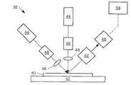
一実施態様は、試料の少なくとも2つの特性を判別するように構成できるシステムに関係する。このシステムは、その試料を支持するように構成されたステージを含むことができる。このシステムはさらに、そのステージに結合された測定具を備えることもできる。測定具は、エネルギーを試料の表面に向けるように構成された照明システムを備えることができる。測定具は、さらに、照明システムに結合された検出システムを備えることもできる。検出システムは、試料の表面から伝搬されるエネルギーを検出するように構成することができる。測定具はさらに、検出されたエネルギーに対して1つまたは複数の出力信号を生成するように構成することもできる。このシステムはさらに、測定具に結合されたプロセッサを備えることもできる。プロセッサは、1つまたは複数の出力信号から試料の少なくとも第1の特性と第2の特性を判別するように構成することができる。
【0009】
一実施態様では、第1の特性は試料の限界寸法を含むことができる。第2の特性には、試料のオーバーレイ・ミスレジストレーションを含めることができる。さらに、プロセッサは、1つまたは複数の出力信号から試料の第3および/または第4の特性を判別するように構成することができる。例えば、試料の第3の特性は試料の欠陥の有無を含み、試料の第4の特性は試料の平坦さの測定結果を含むことができる。一実施態様では測定具は、非結像スキャタロメータ、スキャタロメータ、分光スキャタロメータ、反射率計、分光反射率計、偏光解析器、分光偏光解析器、明視野撮像デバイス、暗視野撮像デバイス、明視野暗視野撮像デバイス、明視野非結像デバイス、暗視野非結像デバイス、明視野暗視野非結像デバイス、コヒーレンス・プローブ顕微鏡、干渉顕微鏡、光学プロフィルメータ、またはそれらの任意の組み合わせを備えることができる。このようにして、測定具は単一の測定具としてまたは複数の測定具として機能するように構成することができる。複数の測定具をシステムの単一の測定具に組み込むことができるため、例えば、第1の測定具の光学要素はさらに第2の測定具の光学要素とすることもできる。
【0010】
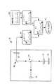
一実施態様では、プロセッサは測定具に結合されたローカル・プロセッサおよび/またはローカル・プロセッサに結合されたリモート・コントローラ・コンピュータを備えることができる。ローカル・プロセッサは、少なくとも一部は、1つまたは複数の出力信号を処理するように構成することができる。リモート・コントローラ・コンピュータは、ローカル・プロセッサから少なくとも一部は処理された1つまたは複数の出力信号を受信するように構成することができる。さらに、リモート・コントローラ・コンピュータは、少なくとも一部は処理された1つまたは複数の出力信号から試料の少なくとも第1の特性と第2の特性を判別するように構成することができる。さらに、リモート・コントローラ・コンピュータは、少なくとも一部は処理された1つまたは複数の出力信号から試料の第3の特性および/または第4の特性を判別するように構成することができる。他の実施態様では、リモート・コントローラ・コンピュータを半導体製造プロセス・ツールなどのプロセス・ツールに結合することができる。このようにして、リモート・コントローラ・コンピュータはさらに、インサイチュー制御手法、フィードバック制御手法、またはフィードフォワード制御手法を使用して試料の少なくとも判別された第1または第2の特性に対して半導体製造プロセス・ツールに結合された1つまたは複数の計測器のパラメータを変更するように構成することができる。
【0011】
他の実施態様は、試料の少なくとも2つの特性を判別する方法に関係する。この方法は、ステージに試料を配置するステップを含むことができる。ステージを測定具に結合することができる。測定具は、照明システムと検出システムを備えることもできる。さらに、この方法は、エネルギーを試料の表面に向けるステップも含む。この方法はさらに、試料の表面から伝搬されるエネルギーを検出するステップも含むことができる。この方法はさらに、検出されたエネルギーに対して1つまたは複数の出力信号を生成するステップを含むこともできる。さらに、この方法は、1つまたは複数の出力信号を処理して試料の少なくとも第1の特性と第2の特性を判別するステップを含むことができる。
【0012】
一実施態様では、第1の特性は試料の限界寸法を含むことができる。第2の特性には、試料のオーバーレイ・ミスレジストレーションを含めることができる。さらに、この方法は、1つまたは複数の出力信号を処理して試料の第3および/または第4の特性を判別するステップを含むことができる。例えば、試料の第3および第4の特性は試料の欠陥の有無および試料の平坦さの測定結果を含むことができる。他の実施態様では、半導体デバイスをこの方法で製造することができる。例えば、この方法は、試料の上に半導体デバイスの一部を形成するステップも含むことができる。
【0013】
一実施態様では、1つまたは複数の出力信号を処理して試料の少なくとも第1の特性と第2の特性を判別するステップに、ローカル・プロセッサを使用して1つまたは複数の出力信号を少なくとも一部は処理するステップを含めることができる。ローカル・プロセッサを測定具に結合することができる。1つまたは複数の出力信号を処理するステップがさらに、ローカル・プロセッサからの一部処理された1つまたは複数の出力信号をリモート・コントローラ・コンピュータに送信するステップを含むことができる。さらに、1つまたは複数の出力信号を処理するステップは、リモート・コントローラ・コンピュータを使用して一部処理された1つまたは複数の出力信号をさらに処理するステップを含むことができる。他の実施態様では、リモート・コントローラ・コンピュータを半導体製造プロセス・ツールなどのプロセス・ツールに結合することができる。このようにして、この方法は試料の少なくとも判別された第1または第2の特性に対してリモート・コントローラ・コンピュータを使用してプロセス・ツールに結合された1つまたは複数の計測器のパラメータを変更するステップを含むことができる。計測器のパラメータを変更するステップは、インサイチュー制御手法、フィードバック制御手法、またはフィードフォワード制御手法を使用するステップを含むことができる。
【0014】
他の実施態様は、試料の少なくとも2つの特性を判別するように構成されたシステムを制御するコンピュータ実装方法に関係する。このシステムは測定具を備えることができる。このようにして、システムを制御するステップは、測定具を制御するステップを含むことができる。さらに、測定具は、照明システムと検出システムを備えることもできる。測定具はステージに結合することができる。測定具を制御するステップは、照明システムを制御してエネルギーを試料の表面に向けるステップを含むことができる。さらに、測定具を制御するステップは、検出システムを制御して試料の表面から伝搬するエネルギーを検出するステップを含むことができる。この方法はさらに、検出されたエネルギーに対して1つまたは複数の出力信号を生成するステップを含むこともできる。コンピュータ実装方法は、さらに、1つまたは複数の出力信号を処理して試料の少なくとも第1の特性と第2の特性を判別するステップを含むことができる。例えば、第1の特性は試料の限界寸法を含むことができる。さらに、第2の特性には、試料のオーバーレイ・ミスレジストレーションを含めることができる。コンピュータにより実施された方法は、1つまたは複数の出力信号を処理して試料の第3および/または第4の特性を判別するステップを含むことができる。実施例では、試料の第3および第4の特性は試料の欠陥の有無および試料の平坦さの測定結果を含むことができる。
【0015】
一実施態様は、試料の少なくとも2つの特性を判別するように構成されたシステムに関係する。このシステムは、その試料を支持するように構成されたステージを含むことができる。このシステムはさらに、そのステージに結合された測定具を備えることもできる。測定具は、エネルギーを試料の表面に向けるように構成された照明システムを備えることができる。測定具は、さらに、照明システムに結合された検出システムを備えることもできる。検出システムは、試料の表面から伝搬されるエネルギーを検出するように構成することができる。測定具はさらに、検出されたエネルギーに対して1つまたは複数の出力信号を生成するように構成することもできる。このシステムはさらに、測定具に結合されたプロセッサを備えることもできる。プロセッサは、1つまたは複数の出力信号から試料の少なくとも第1の特性と第2の特性を判別するように構成することができる。
【0016】
一実施態様では、第1の特性は試料の欠陥の有無を含むことができる。第2の特性には、試料の薄膜特性を含めることができる。さらに、プロセッサは、1つまたは複数の出力信号から試料の他の特性を判別するように構成することができる。一実施態様では測定具は、非結像スキャタロメータ、スキャタロメータ、分光スキャタロメータ、反射率計、分光反射率計、偏光解析器、分光偏光解析器、ビーム・プロフィル偏光解析器、明視野撮像デバイス、暗視野撮像デバイス、明視野暗視野撮像デバイス、明視野非結像デバイス、暗視野非結像デバイス、明視野暗視野非結像デバイス、二重暗視野デバイス、二重分光光度計、コヒーレンス・プローブ顕微鏡、干渉顕微鏡、光学プロフィルメータ、またはそれらの任意の組み合わせを備えることができる。このようにして、測定具は単一の測定具としてまたは複数の測定具として機能するように構成することができる。複数の測定具をシステムの単一の測定具に組み込むことができるため、例えば、第1の測定具の光学要素はさらに第2の測定具の光学要素とすることもできる。
【0017】
一実施態様では、プロセッサは測定具に結合されたローカル・プロセッサおよびローカル・プロセッサに結合されたリモート・コントローラ・コンピュータを備えることができる。ローカル・プロセッサは、少なくとも一部は、1つまたは複数の出力信号を処理するように構成することができる。リモート・コントローラ・コンピュータは、プロセッサから少なくとも一部は処理された1つまたは複数の出力信号を受信するように構成することができる。さらに、リモート・コントローラ・コンピュータは、少なくとも一部は処理された1つまたは複数の出力信号から試料の少なくとも第1の特性と第2の特性を判別するように構成することができる。さらに、リモート・コントローラ・コンピュータは、少なくとも一部は処理された1つまたは複数の出力信号から試料の追加特性を判別するように構成することができる。他の実施態様では、リモート・コントローラ・コンピュータを半導体製造プロセス・ツールなどのプロセス・ツールに結合することができる。このようにして、リモート・コントローラ・コンピュータはさらに、インサイチュー制御手法、フィードバック制御手法、またはフィードフォワード制御手法を使用して試料の少なくとも判別された第1または第2の特性に対してプロセス・ツールに結合された1つまたは複数の計測器のパラメータを変更するように構成することができる。
【0018】
他の実施態様は、試料の少なくとも2つの特性を判別する方法に関係する。この方法は、ステージに試料を配置するステップを含むことができる。ステージを測定具に結合することができる。測定具は、照明システムと検出システムを備えることもできる。さらに、この方法は、エネルギーを試料の表面に向けるステップも含む。この方法はさらに、試料の表面から伝搬されるエネルギーを検出するステップも含むことができる。この方法はさらに、検出されたエネルギーに対して1つまたは複数の出力信号を生成するステップを含むこともできる。さらに、この方法は、1つまたは複数の出力信号を処理して試料の少なくとも第1の特性と第2の特性を判別するステップを含むことができる。
【0019】
一実施態様では、第1の特性は試料の欠陥の有無を含むことができる。第2の特性には、試料の薄膜特性を含めることができる。さらに、プロセッサは、1つまたは複数の出力信号から試料の他の特性を判別するように構成することができる。他の実施態様では、半導体デバイスをこの方法で製造することができる。例えば、この方法は、試料の上に半導体デバイスの一部を形成するステップも含むことができる。
【0020】
一実施態様では、1つまたは複数の出力信号を処理して試料の少なくとも第1の特性と第2の特性を判別するステップに、ローカル・プロセッサを使用して1つまたは複数の出力信号を少なくとも一部処理するステップを含めることができる。ローカル・プロセッサを測定具に結合することができる。1つまたは複数の出力信号を処理するステップがさらに、ローカル・プロセッサからの一部処理された1つまたは複数の出力信号をリモート・コントローラ・コンピュータに送信するステップを含むことができる。さらに、1つまたは複数の出力信号を処理するステップは、リモート・コントローラ・コンピュータを使用して一部処理された1つまたは複数の出力信号をさらに処理するステップを含むことができる。他の実施態様では、リモート・コントローラ・コンピュータを半導体製造プロセス・ツールなどのプロセス・ツールに結合することができる。このようにして、この方法は試料の少なくとも判別された第1または第2の特性に対してリモート・コントローラ・コンピュータを使用してプロセス・ツールに結合された1つまたは複数の計測器のパラメータを変更するステップを含むことができる。計測器のパラメータを変更するステップは、インサイチュー制御手法、フィードバック制御手法、またはフィードフォワード制御手法を使用するステップを含むことができる。
【0021】
他の実施態様は、試料の少なくとも2つの特性を判別するように構成されたシステムを制御するコンピュータ実装方法に関係する。このシステムは測定具を備えることができる。このようにして、システムを制御するステップは、測定具を制御するステップを含むことができる。さらに、測定具は、照明システムと検出システムを備えることもできる。測定具はステージに結合することができる。測定具を制御するステップは、照明システムを制御してエネルギーを試料の表面に向けるステップを含むことができる。さらに、測定具を制御するステップは、検出システムを制御して試料の表面から伝搬するエネルギーを検出するステップを含むことができる。この方法はさらに、検出されたエネルギーに対して1つまたは複数の出力信号を生成するステップを含むこともできる。コンピュータ実装方法は、さらに、1つまたは複数の出力信号を処理して試料の少なくとも第1の特性と第2の特性を判別するステップを含むことができる。例えば、第1の特性は試料の欠陥の有無を含むことができる。第2の特性には、試料の薄膜特性を含めることができる。さらに、プロセッサは、1つまたは複数の出力信号から試料の他の特性を判別するように構成することができる。
【0022】
一実施態様は、試料の少なくとも2つの特性を判別するように構成されたシステムに関係する。このシステムは、その試料を支持するように構成されたステージを含むことができる。このシステムはさらに、そのステージに結合された測定具を備えることもできる。測定具は、エネルギーを試料の表面に向けるように構成された照明システムを備えることができる。測定具は、さらに、照明システムに結合された検出システムを備えることもできる。検出システムは、試料の表面から伝搬されるエネルギーを検出するように構成することができる。測定具はさらに、検出されたエネルギーに対して1つまたは複数の出力信号を生成するように構成することもできる。このシステムはさらに、測定具に結合されたプロセッサを備えることもできる。プロセッサは、1つまたは複数の出力信号から試料の少なくとも第1の特性と第2の特性を判別するように構成することができる。
【0023】
一実施態様では、第1の特性は試料の欠陥の有無を含むことができる。第2の特性には、試料の限界寸法を含めることができる。さらに、プロセッサは、1つまたは複数の出力信号から試料の他の特性を判別するように構成することができる。一実施態様では測定具は、非結像スキャタロメータ、スキャタロメータ、分光スキャタロメータ、反射率計、分光反射率計、偏光解析器、分光偏光解析器、明視野撮像デバイス、暗視野撮像デバイス、明視野暗視野撮像デバイス、明視野非結像デバイス、暗視野非結像デバイス、明視野暗視野非結像デバイス、コヒーレンス・プローブ顕微鏡、干渉顕微鏡、光学プロフィルメータ、またはそれらの任意の組み合わせを備えることができる。このようにして、測定具は単一の測定具としてまたは複数の測定具として機能するように構成することができる。複数の測定具をシステムの単一の測定具に組み込むことができるため、例えば、第1の測定具の光学要素はさらに第2の測定具の光学要素とすることもできる。
【0024】
一実施態様では、プロセッサは測定具に結合されたローカル・プロセッサおよびローカル・プロセッサに結合されたリモート・コントローラ・コンピュータを備えることができる。ローカル・プロセッサは、少なくとも一部は、1つまたは複数の出力信号を処理するように構成することができる。リモート・コントローラ・コンピュータは、プロセッサから少なくとも一部は処理された1つまたは複数の出力信号を受信するように構成することができる。さらに、リモート・コントローラ・コンピュータは、少なくとも一部が処理された1つまたは複数の出力信号から試料の少なくとも第1の特性と第2の特性を判別するように構成することができる。さらに、リモート・コントローラ・コンピュータは、少なくとも一部が処理された1つまたは複数の出力信号から試料の追加特性を判別するように構成することができる。他の実施態様では、リモート・コントローラ・コンピュータを半導体製造プロセス・ツールなどのプロセス・ツールに結合することができる。このようにして、リモート・コントローラ・コンピュータはさらに、インサイチュー制御手法、フィードバック制御手法、および/またはフィードフォワード制御手法を使用して試料の少なくとも判別された第1または第2の特性に対してプロセス・ツールに結合された1つまたは複数の計測器のパラメータを変更するように構成することができる。
【0025】
他の実施態様は、試料の少なくとも2つの特性を判別する方法に関係する。この方法は、ステージに試料を配置するステップを含むことができる。ステージを測定具に結合することができる。測定具は、照明システムと検出システムを備えることもできる。さらに、この方法は、照明システムを使用してエネルギーを試料の表面に向けるステップも含む。この方法はさらに、検出システムを使用して試料の表面から伝搬されるエネルギーを検出するステップも含むことができる。この方法はさらに、検出されたエネルギーに対して1つまたは複数の出力信号を生成するステップを含むこともできる。さらに、この方法は、1つまたは複数の出力信号を処理して試料の少なくとも第1の特性と第2の特性を判別するステップを含むことができる。
【0026】
一実施態様では、第1の特性は試料の欠陥の有無を含むことができる。第2の特性には、試料の限界寸法を含めることができる。さらに、プロセッサは、1つまたは複数の出力信号から試料の他の特性を判別するように構成することができる。他の実施態様では、半導体デバイスをこの方法で製造することができる。例えば、この方法は、半導体基板などの試料の上に半導体デバイスの一部を形成するステップも含むことができる。
【0027】
一実施態様では、1つまたは複数の出力信号を処理して試料の少なくとも第1の特性と第2の特性を判別するステップに、ローカル・プロセッサを使用して1つまたは複数の出力信号を少なくとも一部処理するステップを含めることができる。ローカル・プロセッサを測定具に結合することができる。1つまたは複数の出力信号を処理するステップがさらに、ローカル・プロセッサからの一部処理された1つまたは複数の出力信号をリモート・コントローラ・コンピュータに送信するステップを含むことができる。さらに、1つまたは複数の出力信号を処理するステップは、リモート・コントローラ・コンピュータを使用して一部処理された1つまたは複数の出力信号をさらに処理するステップを含むことができる。他の実施態様では、リモート・コントローラ・コンピュータを半導体製造プロセス・ツールなどのプロセス・ツールに結合することができる。このようにして、この方法は試料の少なくとも判別された第1または第2の特性に対してリモート・コントローラ・コンピュータを使用してプロセス・ツールに結合された1つまたは複数の計測器のパラメータを変更するステップを含むことができる。計測器のパラメータを変更するステップは、インサイチュー制御手法、フィードバック制御手法、および/またはフィードフォワード制御手法を使用するステップを含むことができる。
【0028】
他の実施態様は、試料の少なくとも2つの特性を判別するように構成されたシステムを制御するコンピュータ実装方法に関係する。このシステムは測定具を備えることができる。このようにして、システムを制御するステップは、測定具を制御するステップを含むことができる。さらに、測定具は、照明システムと検出システムを備えることもできる。測定具はステージに結合することができる。測定具を制御するステップは、照明システムを制御してエネルギーを試料の表面に向けるステップを含むことができる。さらに、測定具を制御するステップは、検出システムを制御して試料の表面から伝搬するエネルギーを検出するステップを含むことができる。この方法はさらに、検出されたエネルギーに対して1つまたは複数の出力信号を生成するステップを含むこともできる。コンピュータ実装方法は、さらに、1つまたは複数の出力信号を処理して試料の少なくとも第1の特性と第2の特性を判別するステップを含むことができる。例えば、第1の特性は試料の欠陥の有無を含むことができる。第2の特性には、試料の限界寸法を含めることができる。さらに、プロセッサは、1つまたは複数の出力信号から試料の他の特性を判別するように構成することができる。
【0029】
一実施態様は、試料の少なくとも2つの特性を判別するように構成されたシステムに関係する。このシステムは、その試料を支持するように構成されたステージを含むことができる。このシステムはさらに、そのステージに結合された測定具を備えることもできる。測定具は、エネルギーを試料の表面に向けるように構成された照明システムを備えることができる。測定具は、さらに、照明システムに結合された検出システムを備えることもできる。検出システムは、試料の表面から伝搬されるエネルギーを検出するように構成することができる。測定具はさらに、検出されたエネルギーに対して1つまたは複数の出力信号を生成するように構成することもできる。このシステムはさらに、測定具に結合されたプロセッサを備えることもできる。プロセッサは、1つまたは複数の出力信号から試料の少なくとも第1の特性と第2の特性を判別するように構成することができる。
【0030】
一実施態様では、第1の特性は試料の限界寸法を含むことができる。第2の特性には、試料の薄膜特性を含めることができる。さらに、プロセッサは、1つまたは複数の出力信号から試料の他の特性を判別するように構成することができる。一実施態様では測定具は、非結像スキャタロメータ、スキャタロメータ、分光スキャタロメータ、反射率計、分光反射率計、偏光解析器、分光偏光解析器、ビーム・プロフィル偏光解析器、二重ビーム分光光度計、明視野撮像デバイス、暗視野撮像デバイス、明視野暗視野撮像デバイス、明視野および/または暗視野非結像デバイス、コヒーレンス・プローブ顕微鏡、干渉顕微鏡、光学プロフィルメータ、またはそれらの任意の組み合わせを備えることができる。このようにして、測定具は単一の測定具としてまたは複数の測定具として機能するように構成することができる。複数の測定具をシステムの単一の測定具に組み込むことができるため、例えば、第1の測定具の光学要素はさらに第2の測定具の光学要素とすることもできる。
【0031】
一実施態様では、プロセッサは測定具に結合されたローカル・プロセッサおよび/またはローカル・プロセッサに結合されたリモート・コントローラ・コンピュータを備えることができる。ローカル・プロセッサは、少なくとも一部は、1つまたは複数の出力信号を処理するように構成することができる。リモート・コントローラ・コンピュータは、ローカル・プロセッサから少なくとも一部が処理された1つまたは複数の出力信号を受信するように構成することができる。さらに、リモート・コントローラ・コンピュータは、少なくとも一部が処理された1つまたは複数の出力信号から試料の少なくとも第1の特性と第2の特性を判別するように構成することができる。さらに、リモート・コントローラ・コンピュータは、少なくとも一部が処理された1つまたは複数の出力信号から試料の追加特性を判別するように構成することができる。他の実施態様では、リモート・コントローラ・コンピュータを半導体製造プロセス・ツールなどのプロセス・ツールに結合することができる。このようにして、リモート・コントローラ・コンピュータはさらに、インサイチュー制御手法、フィードバック制御手法、および/またはフィードフォワード制御手法を使用して試料の少なくとも判別された第1または第2の特性に対してプロセス・ツールに結合された1つまたは複数の計測器のパラメータを変更するように構成することができる。
【0032】
他の実施態様は、試料の少なくとも2つの特性を判別する方法に関係する。方法は、ステージに試料を配置するステップを含むことができる。ステージを測定具に結合することができる。測定具は、照明システムと検出システムを備えることもできる。さらに、この方法は、照明システムを使用してエネルギーを試料の表面に向けるステップも含む。この方法はさらに、検出システムを使用して試料の表面から伝搬されるエネルギーを検出するステップも含むことができる。この方法はさらに、検出されたエネルギーに対して1つまたは複数の出力信号を生成するステップを含むこともできる。さらに、この方法は、1つまたは複数の出力信号を処理して試料の少なくとも第1の特性と第2の特性を判別するステップを含むことができる。
【0033】
一実施態様では、第1の特性は試料の限界寸法を含むことができる。第2の特性には、試料の薄膜特性を含めることができる。さらに、プロセッサは、1つまたは複数の出力信号から試料の他の特性を判別するように構成することができる。他の実施態様では、半導体デバイスをこの方法で製造することができる。例えば、この方法は、半導体基板などの試料の上に半導体デバイスの一部を形成するステップも含むことができる。
【0034】
一実施態様では、1つまたは複数の出力信号を処理して試料の少なくとも第1の特性と第2の特性を判別するステップに、ローカル・プロセッサを使用して1つまたは複数の出力信号を少なくとも一部処理するステップを含めることができる。ローカル・プロセッサを測定具に結合することができる。1つまたは複数の出力信号を処理するステップがさらに、ローカル・プロセッサからの一部処理された1つまたは複数の出力信号をリモート・コントローラ・コンピュータに送信するステップを含むことができる。さらに、1つまたは複数の出力信号を処理するステップは、リモート・コントローラ・コンピュータを使用して一部処理された1つまたは複数の出力信号をさらに処理するステップを含むことができる。他の実施態様では、リモート・コントローラ・コンピュータを半導体製造プロセス・ツールなどのプロセス・ツールに結合することができる。このようにして、この方法は試料の少なくとも判別された第1または第2の特性に対してリモート・コントローラ・コンピュータを使用してプロセス・ツールに結合された1つまたは複数の計測器のパラメータを変更するステップを含むことができる。計測器のパラメータを変更するステップは、インサイチュー制御手法、フィードバック制御手法、および/またはフィードフォワード制御手法を使用するステップを含むことができる。
【0035】
他の実施態様は、試料の少なくとも2つの特性を判別するように構成されたシステムを制御するコンピュータ実装方法に関係する。このシステムは測定具を備えることができる。このようにして、システムを制御するステップは、測定具を制御するステップを含むことができる。さらに、測定具は、照明システムと検出システムを備えることもできる。測定具はステージに結合することができる。測定具を制御するステップは、照明システムを制御してエネルギーを試料の表面に向けるステップを含むことができる。さらに、測定具を制御するステップは、検出システムを制御して試料の表面から伝搬するエネルギーを検出するステップを含むことができる。この方法はさらに、検出されたエネルギーに対して1つまたは複数の出力信号を生成するステップを含むこともできる。コンピュータ実装方法は、さらに、1つまたは複数の出力信号を処理して試料の少なくとも第1の特性と第2の特性を判別するステップを含むことができる。例えば、第1の特性は試料の限界寸法を含むことができる。第2の特性には、試料の薄膜特性を含めることができる。さらに、プロセッサは、1つまたは複数の出力信号から試料の他の特性を判別するように構成することができる。
【0036】
一実施態様は、試料の少なくとも3つの特性を判別するように構成されたシステムに関係する。このシステムは、その試料を支持するように構成されたステージを含むことができる。このシステムはさらに、そのステージに結合された測定具を備えることもできる。測定具は、エネルギーを試料の表面に向けるように構成された照明システムを備えることができる。測定具は、さらに、照明システムに結合された検出システムを備えることもできる。検出システムは、試料の表面から伝搬されるエネルギーを検出するように構成することができる。測定具はさらに、検出されたエネルギーに対して1つまたは複数の出力信号を生成するように構成することもできる。このシステムはさらに、測定具に結合されたプロセッサを備えることもできる。プロセッサは、1つまたは複数の出力信号から試料の少なくとも第1の特性、第2の特性、および第3の特性を判別するように構成することができる。
【0037】
一実施態様では、第1の特性は試料の限界寸法を含むことができる。第2の特性は試料の欠陥の有無を含むことができる。第3の特性には、試料の薄膜特性を含めることができる。さらに、プロセッサは、1つまたは複数の出力信号から試料の他の特性を判別するように構成することができる。一実施態様では測定具は、非結像スキャタロメータ、スキャタロメータ、分光スキャタロメータ、反射率計、分光反射率計、偏光解析器、分光偏光解析器、ビーム・プロフィル偏光解析器、明視野撮像デバイス、暗視野撮像デバイス、明視野暗視野撮像デバイス、明視野および/または暗視野非結像デバイス、コヒーレンス・プローブ顕微鏡、干渉顕微鏡、光学プロフィルメータ、二重ビーム分光光度計、またはそれらの任意の組み合わせを備えることができる。このようにして、測定具は単一の測定具としてまたは複数の測定具として機能するように構成することができる。複数の測定具をシステムの単一の測定具に組み込むことができるため、例えば、第1の測定具の光学要素はさらに第2の測定具の光学要素とすることもできる。
【0038】
一実施態様では、プロセッサは測定具に結合されたローカル・プロセッサおよび/またはローカル・プロセッサに結合されたリモート・コントローラ・コンピュータを備えることができる。ローカル・プロセッサは、少なくとも一部は、1つまたは複数の出力信号を処理するように構成することができる。リモート・コントローラ・コンピュータは、プロセッサから少なくとも一部が処理された1つまたは複数の出力信号を受信するように構成することができる。さらに、リモート・コントローラ・コンピュータは、少なくとも一部が処理された1つまたは複数の出力信号から試料の少なくとも第1の特性、第2の特性、および第3の特性を判別するように構成することができる。さらに、リモート・コントローラ・コンピュータは、少なくとも一部が処理された1つまたは複数の出力信号から試料の追加特性を判別するように構成することができる。他の実施態様では、リモート・コントローラ・コンピュータを半導体製造プロセス・ツールなどのプロセス・ツールに結合することができる。このようにして、リモート・コントローラ・コンピュータはさらに、インサイチュー制御手法、フィードバック制御手法、および/またはフィードフォワード制御手法を使用して試料の少なくとも判別された第1、第2、または第3の特性に対して半導体製造プロセス・ツールに結合された1つまたは複数の計測器のパラメータを変更するように構成することができる。
【0039】
他の実施態様は、試料の少なくとも3つの特性を判別する方法に関係する。この方法は、ステージに試料を配置するステップを含むことができる。ステージを測定具に結合することができる。測定具は、照明システムと検出システムを備えることもできる。さらに、この方法は、照明システムを使用してエネルギーを試料の表面に向けるステップも含む。この方法はさらに、検出システムを使用して試料の表面から伝搬されるエネルギーを検出するステップも含むことができる。この方法はさらに、検出されたエネルギーに対して1つまたは複数の出力信号を生成するステップを含むこともできる。さらに、この方法は、1つまたは複数の出力信号を処理して試料の少なくとも第1の特性、第2の特性、および第3の特性を判別するステップを含むことができる。
【0040】
一実施態様では、第1の特性は試料の限界寸法を含むことができる。第2の特性は試料の欠陥の有無を含むことができる。第3の特性には、試料の薄膜特性を含めることができる。さらに、プロセッサは、1つまたは複数の出力信号から試料の他の特性を判別するように構成することができる。他の実施態様では、半導体デバイスをこの方法で製造することができる。例えば、この方法は、半導体基板などの試料の上に半導体デバイスの一部を形成するステップを含むことができる。
【0041】
一実施態様では、1つまたは複数の出力信号を処理して試料の少なくとも第1の特性、第2の特性、および第3の特性を判別するステップに、ローカル・プロセッサを使用して1つまたは複数の出力信号を少なくとも一部処理するステップを含めることができる。ローカル・プロセッサを測定具に結合することができる。1つまたは複数の出力信号を処理するステップがさらに、ローカル・プロセッサからの一部処理された1つまたは複数の出力信号をリモート・コントローラ・コンピュータに送信するステップを含むことができる。さらに、1つまたは複数の出力信号を処理するステップは、リモート・コントローラ・コンピュータを使用して一部処理された1つまたは複数の出力信号をさらに処理するステップを含むことができる。他の実施態様では、リモート・コントローラ・コンピュータを半導体製造プロセス・ツールなどのプロセス・ツールに結合することができる。このようにして、この方法は試料の少なくとも判別された第1または第2の特性に対してリモート・コントローラ・コンピュータを使用してプロセス・ツールに結合された1つまたは複数の計測器のパラメータを変更するステップを含むことができる。計測器のパラメータを変更するステップは、インサイチュー制御手法、フィードバック制御手法、および/またはフィードフォワード制御手法を使用するステップを含むことができる。
【0042】
他の実施態様は、試料の少なくとも3つの特性を判別するように構成されたシステムを制御するコンピュータ実装方法に関係する。このシステムは測定具を備えることができる。このようにして、システムを制御するステップは、測定具を制御するステップを含むことができる。さらに、測定具は、照明システムと検出システムを備えることができる。測定具はステージに結合することができる。測定具を制御するステップは、照明システムを制御してエネルギーを試料の表面に向けるステップを含むことができる。さらに、測定具を制御するステップは、検出システムを制御して試料の表面から伝搬するエネルギーを検出するステップを含むことができる。この方法はさらに、検出されたエネルギーに対して1つまたは複数の出力信号を生成するステップを含むこともできる。コンピュータ実装方法は、さらに、1つまたは複数の出力信号を処理して試料の少なくとも第1の特性、第2の特性、および第3の特性を判別するステップを含むことができる。例えば、第1の特性は試料の限界寸法を含むことができる。第2の特性は試料の欠陥の有無を含むことができる。第3の特性には、試料の薄膜特性を含めることができる。さらに、プロセッサは、1つまたは複数の出力信号から試料の他の特性を判別するように構成することができる。
【0043】
一実施態様は、試料の少なくとも2つの特性を判別するように構成されたシステムに関係する。このシステムは、その試料を支持するように構成されたステージを含む。このシステムはさらに、そのステージに結合された測定具を備えることもできる。測定具は、エネルギーを試料の表面に向けるように構成された照明システムを備えることができる。測定具は、さらに、照明システムに結合された検出システムを備えることもできる。検出システムは、試料の表面から伝搬されるエネルギーを検出するように構成することができる。測定具はさらに、検出されたエネルギーに対して1つまたは複数の出力信号を生成するように構成することもできる。このシステムはさらに、測定具に結合されたプロセッサを備えることもできる。プロセッサは、1つまたは複数の出力信号から試料の少なくとも第1の特性と第2の特性を判別するように構成することができる。
【0044】
一実施態様では、第1の特性は試料上の目立った欠陥の有無を含むことができる。第2の特性は試料上の目立った欠陥の有無を含むことができる。さらに、プロセッサは、1つまたは複数の出力信号から試料の他の特性を判別するように構成することができる。一実施態様では測定具は、非結像スキャタロメータ、スキャタロメータ、分光スキャタロメータ、反射率計、分光反射率計、偏光解析器、分光偏光解析器、明視野撮像デバイス、暗視野撮像デバイス、明視野暗視野撮像デバイス、明視野および/または暗視野非結像デバイス、二重暗視野デバイス、コヒーレンス・プローブ顕微鏡、干渉顕微鏡、光学プロフィルメータ、またはそれらの任意の組み合わせを備えることができる。このようにして、測定具は単一の測定具としてまたは複数の測定具として機能するように構成することができる。複数の測定具をシステムの単一の測定具に組み込むことができるため、例えば、第1の測定具の光学要素はさらに第2の測定具の光学要素とすることもできる。
【0045】
一実施態様では、プロセッサは測定具に結合されたローカル・プロセッサまたはローカル・プロセッサに結合されたリモート・コントローラ・コンピュータを備えることができる。ローカル・プロセッサは、少なくとも一部は、1つまたは複数の出力信号を処理するように構成することができる。リモート・コントローラ・コンピュータは、プロセッサから少なくとも一部は処理された1つまたは複数の出力信号を受信するように構成することができる。さらに、リモート・コントローラ・コンピュータは、少なくとも一部が処理された1つまたは複数の出力信号から試料の少なくとも第1の特性と第2の特性を判別するように構成することができる。さらに、リモート・コントローラ・コンピュータは、少なくとも一部が処理された1つまたは複数の出力信号から試料の追加特性を判別するように構成することができる。他の実施態様では、リモート・コントローラ・コンピュータを半導体製造プロセス・ツールなどのプロセス・ツールに結合することができる。このようにして、リモート・コントローラ・コンピュータはさらに、インサイチュー制御手法、フィードバック制御手法、および/またはフィードフォワード制御手法を使用して試料の少なくとも判別された第1または第2の特性に対してプロセス・ツールに結合された1つまたは複数の計測器のパラメータを変更するように構成することができる。
【0046】
他の実施態様は、試料の少なくとも2つの特性を判別する方法に関係する。この方法は、ステージに試料を配置するステップを含むことができる。ステージを測定具に結合することができる。測定具は、照明システムと検出システムを備えることもできる。さらに、この方法は、照明システムを使用してエネルギーを試料の表面に向けるステップを含むことができる。この方法はさらに、検出システムを使用して試料の表面から伝搬されるエネルギーを検出するステップも含むことができる。この方法はさらに、検出されたエネルギーに対して1つまたは複数の出力信号を生成するステップを含むこともできる。さらに、この方法は、1つまたは複数の出力信号を処理して試料の少なくとも第1の特性と第2の特性を判別するステップを含むことができる。
【0047】
一実施態様では、第1の特性は試料上の目立った欠陥の有無を含むことができる。第2の特性は試料上の目立った欠陥の有無であってよい。さらに、プロセッサは、1つまたは複数の出力信号から試料の他の特性を判別するように構成することができる。他の実施態様では、半導体デバイスをこの方法で製造することができる。例えば、この方法は、半導体基板などの試料の上に半導体デバイスの一部を形成するステップを含むことができる。
【0048】
一実施態様では、1つまたは複数の出力信号を処理して試料の少なくとも第1の特性と第2の特性を判別するステップに、ローカル・プロセッサを使用して1つまたは複数の出力信号を少なくとも一部処理するステップを含めることができる。ローカル・プロセッサを測定具に結合することができる。1つまたは複数の出力信号を処理するステップがさらに、ローカル・プロセッサからの一部処理された1つまたは複数の出力信号をリモート・コントローラ・コンピュータに送信するステップを含むことができる。さらに、1つまたは複数の出力信号を処理するステップは、リモート・コントローラ・コンピュータを使用して一部処理された1つまたは複数の出力信号をさらに処理するステップを含むことができる。他の実施態様では、リモート・コントローラ・コンピュータを半導体製造プロセス・ツールなどのプロセス・ツールに結合することができる。このようにして、この方法は試料の少なくとも判別された第1または第2の特性に対してリモート・コントローラ・コンピュータを使用してプロセス・ツールに結合された1つまたは複数の計測器のパラメータを変更するステップを含むことができる。計測器のパラメータを変更するステップは、インサイチュー制御手法、フィードバック制御手法、および/またはフィードフォワード制御手法を使用するステップを含むことができる。
【0049】
他の実施態様は、試料の少なくとも2つの特性を判別するように構成されたシステムを制御するコンピュータ実装方法に関係する。このシステムは測定具を備えることができる。このようにして、システムを制御するステップは、測定具を制御するステップを含むことができる。さらに、測定具は、照明システムと検出システムを備えることもできる。測定具はステージに結合することができる。測定具を制御するステップは、照明システムを制御してエネルギーを試料の表面に向けるステップを含むことができる。さらに、測定具を制御するステップは、検出システムを制御して試料の表面から伝搬するエネルギーを検出するステップを含むことができる。この方法はさらに、検出されたエネルギーに対して1つまたは複数の出力信号を生成するステップを含むこともできる。コンピュータ実装方法は、さらに、1つまたは複数の出力信号を処理して試料の少なくとも第1の特性と第2の特性を判別するステップを含むことができる。例えば、第1の特性は試料上の目立った欠陥の有無を含むことができる。第2の特性は試料上の目立った欠陥の有無であってよい。さらに、プロセッサは、1つまたは複数の出力信号から試料の他の特性を判別するように構成することができる。
【0050】
一実施態様は、試料の少なくとも3つの特性を判別するように構成されたシステムに関係する。このシステムは、その試料を支持するように構成されたステージを含むことができる。このシステムはさらに、そのステージに結合された測定具を備えることもできる。測定具は、エネルギーを試料の表面に向けるように構成された照明システムを備えることができる。測定具は、さらに、照明システムに結合された検出システムを備えることもできる。検出システムは、試料の表面から伝搬されるエネルギーを検出するように構成することができる。測定具はさらに、検出されたエネルギーに対して1つまたは複数の出力信号を生成するように構成することもできる。このシステムはさらに、測定具に結合されたプロセッサを備えることもできる。プロセッサは、1つまたは複数の出力信号から試料の少なくとも第1の特性、第2の特性、および第3の特性を判別するように構成することができる。
【0051】
一実施態様では、第1の特性は試料の平坦さ測定結果を含むことができる。第2の特性は試料の欠陥の有無に関する情報を含むことができる。第3の特性には、試料の薄膜特性を含めることができる。さらに、プロセッサは、1つまたは複数の出力信号から試料の他の特性を判別するように構成することができる。一実施態様では測定具は、非結像スキャタロメータ、スキャタロメータ、分光スキャタロメータ、反射率計、分光反射率計、偏光解析器、分光偏光解析器、ビーム・プロフィル偏光解析器、明視野および/または暗視野撮像デバイス、明視野および/または暗視野非結像デバイス、二重暗視野デバイス、コヒーレンス・プローブ顕微鏡、干渉顕微鏡、干渉計、光学プロフィルメータ、二重ビーム分光光度計、またはそれらの任意の組み合わせを備えることができる。このようにして、測定具は単一の測定具としてまたは複数の測定具として機能するように構成することができる。複数の測定具をシステムの単一の測定具に組み込むことができるため、例えば、第1の測定具の光学要素はさらに第2の測定具の光学要素とすることもできる。
【0052】
一実施態様では、プロセッサは測定具に結合されたローカル・プロセッサおよびローカル・プロセッサに結合されたリモート・コントローラ・コンピュータを備えることができる。ローカル・プロセッサは、1つまたは複数の出力信号を少なくとも一部処理するように構成することができる。リモート・コントローラ・コンピュータは、プロセッサから少なくとも一部が処理された1つまたは複数の出力信号を受信するように構成することができる。さらに、リモート・コントローラ・コンピュータは、少なくとも一部が処理された1つまたは複数の出力信号から試料の少なくとも第1の特性、第2の特性、および第3の特性を判別するように構成することができる。さらに、リモート・コントローラ・コンピュータは、少なくとも一部が処理された1つまたは複数の出力信号から試料の追加特性を判別するように構成することができる。他の実施態様では、リモート・コントローラ・コンピュータを半導体製造プロセス・ツールなどのプロセス・ツールに結合することができる。このようにして、リモート・コントローラ・コンピュータはさらに、インサイチュー制御手法、フィードバック制御手法、および/またはフィードフォワード制御手法を使用して試料の少なくとも判別された第1、第2、または第3の特性に対してプロセス・ツールに結合された1つまたは複数の計測器のパラメータを変更するように構成することができる。
【0053】
他の実施態様は、試料の少なくとも3つの特性を判別する方法に関係する。この方法は、ステージに試料を配置するステップを含むことができる。ステージを測定具に結合することができる。測定具は、照明システムと検出システムを備えることもできる。さらに、この方法は、照明システムを使用してエネルギーを試料の表面に向けるステップも含むことができる。この方法はさらに、検出システムを使用して試料の表面から伝搬されるエネルギーを検出するステップも含むことができる。この方法はさらに、検出されたエネルギーに対して1つまたは複数の出力信号を生成するステップを含むことができる。さらに、この方法は、1つまたは複数の出力信号を処理して試料の少なくとも第1の特性、第2の特性、および第3の特性を判別するステップを含むことができる。
【0054】
一実施態様では、第1の特性は試料の平坦さ測定結果を含むことができる。第2の特性は試料の欠陥の有無を含むことができる。第3の特性には、試料の薄膜特性を含めることができる。さらに、プロセッサは、1つまたは複数の出力信号から試料の他の特性を判別するように構成することができる。他の実施態様では、半導体デバイスをこの方法で製造することができる。例えば、この方法は、半導体基板などの試料の上に半導体デバイスの一部を形成するステップを含むことができる。
【0055】
一実施態様では、1つまたは複数の出力信号を処理して試料の少なくとも第1の特性、第2の特性、および第3の特性を判別するステップに、ローカル・プロセッサを使用して1つまたは複数の出力信号を少なくとも一部処理するステップを含めることができる。ローカル・プロセッサを測定具に結合することができる。1つまたは複数の出力信号を処理するステップがさらに、ローカル・プロセッサからの一部処理された1つまたは複数の出力信号をリモート・コントローラ・コンピュータに送信するステップを含むことができる。さらに、1つまたは複数の出力信号を処理するステップは、リモート・コントローラ・コンピュータを使用して一部処理された1つまたは複数の出力信号をさらに処理するステップを含むことができる。他の実施態様では、リモート・コントローラ・コンピュータを半導体製造プロセス・ツールなどのプロセス・ツールに結合することができる。このようにして、この方法は試料の少なくとも判別された第1または第2の特性に対してリモート・コントローラ・コンピュータを使用してプロセス・ツールに結合された1つまたは複数の計測器のパラメータを変更するステップを含むことができる。計測器のパラメータを変更するステップは、インサイチュー制御手法、フィードバック制御手法、および/またはフィードフォワード制御手法を使用するステップを含むことができる。
【0056】
他の実施態様は、試料の少なくとも3つの特性を判別するように構成されたシステムを制御するコンピュータ実装方法に関係する。このシステムは測定具を備えることができる。このようにして、システムを制御するステップは、測定具を制御するステップを含むことができる。さらに、測定具は、照明システムと検出システムを備えることもできる。測定具はステージに結合することができる。測定具を制御するステップは、照明システムを制御してエネルギーを試料の表面に向けるステップを含むことができる。さらに、測定具を制御するステップは、検出システムを制御して試料の表面から伝搬するエネルギーを検出するステップを含むことができる。この方法はさらに、検出されたエネルギーに対して1つまたは複数の出力信号を生成するステップを含むこともできる。コンピュータ実装方法は、さらに、1つまたは複数の出力信号を処理して試料の少なくとも第1の特性、第2の特性、および第3の特性を判別するステップを含むことができる。例えば、第1の特性は試料の平坦さ測定結果を含むことができる。第2の特性は試料の欠陥の有無を含むことができる。第3の特性には、試料の薄膜特性を含めることができる。さらに、プロセッサは、1つまたは複数の出力信号から試料の他の特性を判別するように構成することができる。
【0057】
一実施態様は、試料の少なくとも2つの特性を判別するように構成されたシステムに関係する。このシステムは、その試料を支持するように構成されたステージを含む。このシステムはさらに、そのステージに結合された測定具を備えることもできる。測定具は、エネルギーを試料の表面に向けるように構成された照明システムを備えることができる。測定具は、さらに、照明システムに結合された検出システムを備えることもできる。検出システムは、試料の表面から伝搬されるエネルギーを検出するように構成することができる。測定具はさらに、検出されたエネルギーに対して1つまたは複数の出力信号を生成するように構成することもできる。このシステムはさらに、測定具に結合されたプロセッサを備えることもできる。プロセッサは、検出された光から試料の少なくとも第1の特性と第2の特性を判別するように構成することができる。
【0058】
一実施態様では、第1の特性に、試料のオーバーレイ・ミスレジストレーションを含めることができる。第2の特性は試料の平坦さ測定結果を含むことができる。さらに、プロセッサは、1つまたは複数の出力信号から試料の他の特性を判別するように構成することができる。一実施態様では測定具は、非結像スキャタロメータ、スキャタロメータ、分光スキャタロメータ、反射率計、分光反射率計、分光偏光解析器、ビーム・プロフィル偏光解析器、明視野撮像デバイス、暗視野撮像デバイス、明視野暗視野撮像デバイス、コヒーレンス・プローブ顕微鏡、干渉顕微鏡、干渉計、光学プロフィルメータ、二重ビーム分光光度計、またはそれらの任意の組み合わせを備えることができる。このようにして、測定具は単一の測定具としてまたは複数の測定具として機能するように構成することができる。複数の測定具をシステムの単一の測定具に組み込むことができるため、例えば、第1の測定具の光学要素はさらに第2の測定具の光学要素とすることもできる。
【0059】
一実施態様では、プロセッサは測定具に結合されたローカル・プロセッサおよびローカル・プロセッサに結合されたリモート・コントローラ・コンピュータを備えることができる。ローカル・プロセッサは、1つまたは複数の出力信号を少なくとも一部処理するように構成することができる。リモート・コントローラ・コンピュータは、プロセッサから少なくとも一部が処理された1つまたは複数の出力信号を受信するように構成することができる。さらに、リモート・コントローラ・コンピュータは、少なくとも一部が処理された1つまたは複数の出力信号から試料の少なくとも第1の特性と第2の特性を判別するように構成することができる。さらに、リモート・コントローラ・コンピュータは、少なくとも一部が処理された1つまたは複数の出力信号から試料の追加特性を判別するように構成することができる。他の実施態様では、リモート・コントローラ・コンピュータを半導体製造プロセス・ツールなどのプロセス・ツールに結合することができる。このようにして、リモート・コントローラ・コンピュータはさらに、インサイチュー制御手法、フィードバック制御手法、および/またはフィードフォワード制御手法を使用して試料の少なくとも判別された第1または第2の特性に対してプロセス・ツールに結合された1つまたは複数の計測器のパラメータを変更するように構成することができる。
【0060】
他の実施態様は、試料の少なくとも2つの特性を判別する方法に関係する。方法は、ステージに試料を配置するステップを含むことができる。ステージを測定具に結合することができる。測定具は、照明システムと検出システムを備えることができる。さらに、この方法は、照明システムを使用してエネルギーを試料の表面に向けるステップも含むことができる。この方法はさらに、検出システムを使用して試料の表面から伝搬されるエネルギーを検出するステップも含むことができる。この方法はさらに、検出されたエネルギーに対して1つまたは複数の出力信号を生成するステップを含むこともできる。さらに、この方法は、1つまたは複数の出力信号を処理して試料の少なくとも第1の特性と第2の特性を判別するステップを含むことができる。
【0061】
一実施態様では、第1の特性に、試料のオーバーレイ・ミスレジストレーションを含めることができる。第2の特性は試料の平坦さ測定結果を含むことができる。さらに、プロセッサは、1つまたは複数の出力信号から試料の他の特性を判別するように構成することができる。他の実施態様では、半導体デバイスをこの方法で製造することができる。例えば、この方法は、半導体基板などの試料の上に半導体デバイスの一部を形成するステップも含むことができる。
【0062】
一実施態様では、1つまたは複数の出力信号を処理して試料の少なくとも第1の特性と第2の特性を判別するステップに、ローカル・プロセッサを使用して1つまたは複数の出力信号を少なくとも一部処理するステップを含めることができる。ローカル・プロセッサを測定具に結合することができる。1つまたは複数の出力信号を処理するステップがさらに、ローカル・プロセッサからの一部処理された1つまたは複数の出力信号をリモート・コントローラ・コンピュータに送信するステップを含むこともできる。さらに、1つまたは複数の出力信号を処理するステップは、リモート・コントローラ・コンピュータを使用して一部処理された1つまたは複数の出力信号をさらに処理するステップを含むことができる。他の実施態様では、リモート・コントローラ・コンピュータを半導体製造プロセス・ツールなどのプロセス・ツールに結合することができる。このようにして、この方法は試料の少なくとも判別された第1または第2の特性に対してリモート・コントローラ・コンピュータを使用してプロセス・ツールに結合された1つまたは複数の計測器のパラメータを変更するステップを含むことができる。計測器のパラメータを変更するステップは、インサイチュー制御手法、フィードバック制御手法、および/またはフィードフォワード制御手法を使用するステップを含むことができる。
【0063】
他の実施態様は、試料の少なくとも2つの特性を判別するように構成されたシステムを制御するコンピュータ実装方法に関係する。このシステムは測定具を備えることができる。このようにして、システムを制御するステップは、測定具を制御するステップを含むことができる。さらに、測定具は、照明システムと検出システムを備えることもできる。測定具はステージに結合することができる。測定具を制御するステップは、照明システムを制御してエネルギーを試料の表面に向けるステップを含むことができる。さらに、測定具を制御するステップは、検出システムを制御して試料の表面から伝搬するエネルギーを検出するステップを含むことができる。この方法はさらに、検出されたエネルギーに対して1つまたは複数の出力信号を生成するステップを含むこともできる。コンピュータ実装方法は、さらに、1つまたは複数の出力信号を処理して試料の少なくとも第1の特性と第2の特性を判別するステップを含むことができる。例えば、第1の特性に、試料のオーバーレイ・ミスレジストレーションを含めることができる。第2の特性は試料の平坦さ測定結果を含むことができる。さらに、プロセッサは、1つまたは複数の出力信号から試料の他の特性を判別するように構成することができる。
【0064】
一実施態様は、試料の少なくとも2つの特性を判別するように構成されたシステムに関係する。このシステムは、その試料を支持するように構成されたステージを含むことができる。このシステムはさらに、そのステージに結合された測定具を備えることもできる。測定具は、エネルギーを試料の表面に向けるように構成された照明システムを備えることができる。測定具は、さらに、照明システムに結合された検出システムを備えることもできる。検出システムは、試料の表面から伝搬されるエネルギーを検出するように構成することができる。測定具はさらに、検出されたエネルギーに対して1つまたは複数の出力信号を生成するように構成することもできる。このシステムはさらに、測定具に結合されたプロセッサを備えることもできる。プロセッサは、1つまたは複数の出力信号から試料の少なくとも第1の特性と第2の特性を判別するように構成することができる。
【0065】
一実施態様では、第1の特性は試料のイオン注入領域の特性を含むことができる。第2の特性は試料の欠陥の有無を含むことができる。さらに、プロセッサは、1つまたは複数の出力信号から試料の他の特性を判別するように構成することができる。一実施態様では測定具は、変調光学反射率計、X線反射率デバイス、渦電流デバイス、写真音響デバイス、分光偏光解析器、分光反射率計、二重ビーム分光光度計、非結像スキャタロメータ、スキャタロメータ、分光スキャタロメータ、反射率計、偏光解析器、非結像明視野デバイス、非結像暗視野デバイス、非結像明視野暗視野デバイス、明視野撮像デバイス、暗視野撮像デバイス、明視野暗視野撮像デバイス、またはそれらの任意の組み合わせを備えることができる。このようにして、測定具は単一の測定具としてまたは複数の測定具として機能するように構成することができる。複数の測定具をシステムの単一の測定具に組み込むことができるため、例えば、第1の測定具の光学要素はさらに第2の測定具の光学要素とすることもできる。
【0066】
一実施態様では、プロセッサは測定具に結合されたローカル・プロセッサおよびローカル・プロセッサに結合されたリモート・コントローラ・コンピュータを備えることができる。ローカル・プロセッサは、1つまたは複数の出力信号を少なくとも一部処理するように構成することができる。リモート・コントローラ・コンピュータは、プロセッサから少なくとも一部が処理された1つまたは複数の出力信号を受信するように構成することができる。さらに、リモート・コントローラ・コンピュータは、少なくとも一部は処理された1つまたは複数の出力信号から試料の少なくとも第1の特性と第2の特性を判別するように構成することができる。さらに、リモート・コントローラ・コンピュータは、少なくとも一部が処理された1つまたは複数の出力信号から試料の追加特性を判別するように構成することができる。他の実施態様では、リモート・コントローラ・コンピュータを半導体製造プロセス・ツールなどのプロセス・ツールに結合することができる。このようにして、リモート・コントローラ・コンピュータはさらに、インサイチュー制御手法、フィードバック制御手法、および/またはフィードフォワード制御手法を使用して試料の少なくとも判別された第1または第2の特性に対してプロセス・ツールに結合された1つまたは複数の計測器のパラメータを変更するように構成することができる。
【0067】
他の実施態様は、試料の少なくとも2つの特性を判別する方法に関係する。方法は、ステージに試料を配置するステップを含むことができる。ステージを測定具に結合することができる。測定具は、照明システムと検出システムを備えることができる。さらに、この方法は、照明システムを使用してエネルギーを試料の表面に向けるステップも含むことができる。この方法はさらに、検出システムを使用して試料の表面から伝搬されるエネルギーを検出するステップも含むことができる。この方法はさらに、検出されたエネルギーに対して1つまたは複数の出力信号を生成するステップを含むことができる。さらに、この方法は、1つまたは複数の出力信号を処理して試料の少なくとも第1の特性と第2の特性を判別するステップを含むことができる。
【0068】
一実施態様では、第1の特性は試料のイオン注入領域の特性を含むことができる。第2の特性は試料の欠陥の有無を含むことができる。さらに、プロセッサは、1つまたは複数の出力信号から試料の他の特性を判別するように構成することができる。他の実施態様では、半導体デバイスをこの方法で製造することができる。例えば、この方法は、半導体基板などの試料の上に半導体デバイスの一部を形成するステップも含むことができる。
【0069】
一実施態様では、1つまたは複数の出力信号を処理して試料の少なくとも第1の特性と第2の特性を判別するステップに、ローカル・プロセッサを使用して1つまたは複数の出力信号を少なくとも一部処理するステップを含めることができる。ローカル・プロセッサを測定具に結合することができる。1つまたは複数の出力信号を処理するステップがさらに、ローカル・プロセッサからの一部処理された1つまたは複数の出力信号をリモート・コントローラ・コンピュータに送信するステップを含むことができる。さらに、1つまたは複数の出力信号を処理するステップは、リモート・コントローラ・コンピュータを使用して一部処理された1つまたは複数の出力信号をさらに処理するステップを含むことができる。他の実施態様では、リモート・コントローラ・コンピュータを半導体製造プロセス・ツールなどのプロセス・ツールに結合することができる。このようにして、この方法は試料の少なくとも判別された第1または第2の特性に対してリモート・コントローラ・コンピュータを使用して半導体製造プロセス・ツールに結合された1つまたは複数の計測器のパラメータを変更するステップを含むことができる。計測器のパラメータを変更するステップは、インサイチュー制御手法、フィードバック制御手法、および/またはフィードフォワード制御手法を使用するステップを含むことができる。
【0070】
他の実施態様は、試料の少なくとも2つの特性を判別するように構成されたシステムを制御するコンピュータ実装方法に関係する。このシステムは測定具を備えることができる。このようにして、システムを制御するステップは、測定具を制御するステップを含むことができる。さらに、測定具は、照明システムと検出システムを備えることができる。測定具はステージに結合することができる。測定具を制御するステップは、照明システムを制御してエネルギーを試料の表面に向けるステップを含むことができる。さらに、測定具を制御するステップは、検出システムを制御して試料の表面から伝搬するエネルギーを検出するステップを含むことができる。この方法はさらに、検出されたエネルギーに対して1つまたは複数の出力信号を生成するステップを含むこともできる。コンピュータ実装方法は、さらに、1つまたは複数の出力信号を処理して試料の少なくとも第1の特性と第2の特性を判別するステップを含むことができる。例えば、第1の特性は試料のイオン注入領域の特性を含むことができる。第2の特性は試料の欠陥の有無を含むことができる。さらに、プロセッサは、1つまたは複数の出力信号から試料の他の特性を判別するように構成することができる。
【0071】
一実施態様は、試料の少なくとも2つの特性を判別するように構成されたシステムに関係する。このシステムは、その試料を支持するように構成されたステージを含むことができる。このシステムはさらに、そのステージに結合された測定具を備えることもできる。測定具は、エネルギーを試料の表面に向けるように構成された照明システムを備えることができる。測定具は、さらに、照明システムに結合された検出システムを備えることもできる。検出システムは、試料の表面から伝搬されるエネルギーを検出するように構成することができる。測定具は、検出された光に対して1つまたは複数の出力信号を生成するように構成することができる。このシステムはさらに、測定具に結合されたプロセッサを備えることもできる。プロセッサは、1つまたは複数の出力信号から試料の少なくとも第1の特性と第2の特性を判別するように構成することができる。
【0072】
一実施態様では、第1の特性は試料の粘着特性を含むことができる。第2の特性には、試料の厚さを含めることができる。さらに、プロセッサは、1つまたは複数の出力信号から試料の他の特性を判別するように構成することができる。一実施態様では、測定具は、渦電流デバイス、写真音響デバイス、分光偏光解析器、偏光解析器、X線反射率計、グレージングX線反射率計、X線回折計、またはその組み合わせを備えることができる。このようにして、測定具は単一の測定具としてまたは複数の測定具として機能するように構成することができる。複数の測定具をシステムの単一の測定具に組み込むことができるため、例えば、第1の測定具の光学要素はさらに第2の測定具の光学要素とすることもできる。
【0073】
一実施態様では、プロセッサは測定具に結合されたローカル・プロセッサおよびローカル・プロセッサに結合されたリモート・コントローラ・コンピュータを備えることができる。ローカル・プロセッサは、少なくとも一部は、1つまたは複数の出力信号を処理するように構成することができる。リモート・コントローラ・コンピュータは、ローカル・プロセッサから少なくとも一部が処理された1つまたは複数の出力信号を受信するように構成することができる。さらに、リモート・コントローラ・コンピュータは、少なくとも一部が処理された1つまたは複数の出力信号から試料の少なくとも第1の特性と第2の特性を判別するように構成することができる。さらに、リモート・コントローラ・コンピュータは、少なくとも一部が処理された1つまたは複数の出力信号から試料の追加特性を判別するように構成することができる。他の実施態様では、リモート・コントローラ・コンピュータを半導体製造プロセス・ツールなどのプロセス・ツールに結合することができる。このようにして、リモート・コントローラ・コンピュータはさらに、インサイチュー制御手法、フィードバック制御手法、および/またはフィードフォワード制御手法を使用して試料の少なくとも判別された第1または第2の特性に対して半導体製造プロセス・ツールに結合された1つまたは複数の計測器のパラメータを変更するように構成することができる。
【0074】
他の実施態様は、試料の少なくとも2つの特性を判別する方法に関係する。方法は、ステージに試料を配置するステップを含むことができる。ステージを測定具に結合することができる。測定具は、照明システムと検出システムを備えることもできる。さらに、この方法は、照明システムを使用してエネルギーを試料の表面に向けるステップも含むことができる。この方法はさらに、検出システムを使用して試料の表面から伝搬されるエネルギーを検出するステップも含むことができる。この方法はさらに、検出されたエネルギーに対して1つまたは複数の出力信号を生成するステップを含むことができる。さらに、この方法は、1つまたは複数の出力信号を処理して試料の少なくとも第1の特性と第2の特性を判別するステップを含むことができる。
【0075】
一実施態様では、第1の特性は試料の粘着特性を含むことができる。第2の特性には、試料の厚さを含めることができる。さらに、プロセッサは、1つまたは複数の出力信号から試料の他の特性を判別するように構成することができる。他の実施態様では、半導体デバイスをこの方法で製造することができる。例えば、この方法は、半導体基板などの試料の上に半導体デバイスの一部を形成するステップを含むことができる。
【0076】
一実施態様では、1つまたは複数の出力信号を処理して試料の少なくとも第1の特性と第2の特性を判別するステップに、ローカル・プロセッサを使用して1つまたは複数の出力信号を少なくとも一部は処理するステップを含めることができる。ローカル・プロセッサを測定具に結合することができる。1つまたは複数の出力信号を処理するステップがさらに、ローカル・プロセッサからの一部処理された1つまたは複数の出力信号をリモート・コントローラ・コンピュータに送信するステップを含むこともできる。さらに、1つまたは複数の出力信号を処理するステップは、リモート・コントローラ・コンピュータを使用して一部処理された1つまたは複数の出力信号をさらに処理するステップを含むことができる。他の実施態様では、リモート・コントローラ・コンピュータを半導体製造プロセス・ツールなどのプロセス・ツールに結合することができる。このようにして、この方法は試料の少なくとも判別された第1または第2の特性に対してリモート・コントローラ・コンピュータを使用してプロセス・ツールに結合された1つまたは複数の計測器のパラメータを変更するステップを含むことができる。計測器のパラメータを変更するステップは、インサイチュー制御手法、フィードバック制御手法、および/またはフィードフォワード制御手法を使用するステップを含むことができる。
【0077】
他の実施態様は、試料の少なくとも2つの特性を判別するように構成されたシステムを制御するコンピュータ実装方法に関係する。このシステムは測定具を備えることができる。このようにして、システムを制御するステップは、測定具を制御するステップを含むことができる。さらに、測定具は、照明システムと検出システムを備えることができる。測定具はステージに結合することができる。測定具を制御するステップは、照明システムを制御してエネルギーを試料の表面に向けるステップを含むことができる。さらに、測定具を制御するステップは、検出システムを制御して試料の表面から伝搬するエネルギーを検出するステップを含むことができる。この方法はさらに、検出されたエネルギーに対して1つまたは複数の出力信号を生成するステップを含むこともできる。コンピュータ実装方法は、さらに、1つまたは複数の出力信号を処理して試料の少なくとも第1の特性と第2の特性を判別するステップを含むことができる。例えば、第1の特性は試料の粘着特性を含むことができる。第2の特性には、試料の厚さを含めることができる。さらに、プロセッサは、1つまたは複数の出力信号から試料の他の特性を判別するように構成することができる。
【0078】
一実施態様は、試料の少なくとも2つの特性を判別するように構成されたシステムに関係する。このシステムは、その試料を支持するように構成されたステージを含むことができる。このシステムはさらに、そのステージに結合された測定具を備えることもできる。測定具は、エネルギーを試料の表面に向けるように構成された照明システムを備えることができる。測定具は、さらに、照明システムに結合された検出システムを備えることもできる。検出システムは、試料の表面から伝搬されるエネルギーを検出するように構成することができる。測定具はさらに、検出されたエネルギーに対して1つまたは複数の出力信号を生成するように構成することができる。このシステムはさらに、測定具に結合されたプロセッサを備えることもできる。プロセスは、1つまたは複数の出力信号から試料の少なくとも第1の特性と第2の特性を判別するように構成することができる。
【0079】
一実施態様では、第1の特性は試料内の元素の濃度を含むことができる。第2の特性には、試料の厚さを含めることができる。さらに、プロセッサは、1つまたは複数の出力信号から試料の他の特性を判別するように構成することができる。一実施態様では、測定具は、写真音響デバイス、X線反射率計、グレージングX線反射率計、X線回折計、渦電流デバイス、分光偏光解析器、偏光解析器、またはその組み合わせを備えることができる。このようにして、測定具は単一の測定具としてまたは複数の測定具として機能するように構成することができる。複数の測定具をシステムの単一の測定具に組み込むことができるため、例えば、第1の測定具の光学要素はさらに第2の測定具の光学要素とすることもできる。
【0080】
一実施態様では、プロセッサは測定具に結合されたローカル・プロセッサおよびローカル・プロセッサに結合されたリモート・コントローラ・コンピュータを備えることができる。ローカル・プロセッサは、1つまたは複数の出力信号を少なくとも一部処理するように構成することができる。リモート・コントローラ・コンピュータは、プロセッサから少なくとも一部が処理された1つまたは複数の出力信号を受信するように構成することができる。さらに、リモート・コントローラ・コンピュータは、少なくとも一部が処理された1つまたは複数の出力信号から試料の少なくとも第1の特性と第2の特性を判別するように構成することができる。さらに、リモート・コントローラ・コンピュータは、少なくとも一部が処理された1つまたは複数の出力信号から試料の追加特性を判別するように構成することができる。他の実施態様では、リモート・コントローラ・コンピュータを半導体製造プロセス・ツールなどのプロセス・ツールに結合することができる。このようにして、リモート・コントローラ・コンピュータはさらに、インサイチュー制御手法、フィードバック制御手法、および/またはフィードフォワード制御手法を使用して試料の少なくとも判別された第1または第2の特性に対してプロセス・ツールに結合された1つまたは複数の計測器のパラメータを変更するように構成することができる。
【0081】
他の実施態様は、試料の少なくとも2つの特性を判別する方法に関係する。この方法は、ステージに試料を配置するステップを含むことができる。ステージを測定具に結合することができる。測定具は、照明システムと検出システムを備えることもできる。さらに、この方法は、照明システムを使用してエネルギーを試料の表面に向けるステップも含むことができる。この方法はさらに、検出システムを使用して試料の表面から伝搬されるエネルギーを検出するステップも含むことができる。この方法はさらに、検出されたエネルギーに対して1つまたは複数の出力信号を生成するステップを含むこともできる。さらに、この方法は、1つまたは複数の出力信号を処理して試料の少なくとも第1の特性と第2の特性を判別するステップを含むことができる。
【0082】
一実施態様では、第1の特性は試料内の元素の濃度を含むことができる。第2の特性には、試料の厚さを含めることができる。さらに、プロセッサは、1つまたは複数の出力信号から試料の他の特性を判別するように構成することができる。他の実施態様では、半導体デバイスをこの方法で製造することができる。例えば、この方法は、半導体基板などの試料の上に半導体デバイスの一部を形成するステップを含むことができる。
【0083】
一実施態様では、1つまたは複数の出力信号を処理して試料の少なくとも第1の特性と第2の特性を判別するステップに、ローカル・プロセッサを使用して1つまたは複数の出力信号を少なくとも一部処理するステップを含めることができる。ローカル・プロセッサを測定具に結合することができる。1つまたは複数の出力信号を処理するステップがさらに、ローカル・プロセッサからの一部処理された1つまたは複数の出力信号をリモート・コントローラ・コンピュータに送信するステップを含むこともできる。さらに、1つまたは複数の出力信号を処理するステップは、リモート・コントローラ・コンピュータを使用して一部処理された1つまたは複数の出力信号をさらに処理するステップを含むことができる。他の実施態様では、リモート・コントローラ・コンピュータを半導体製造プロセス・ツールなどのプロセス・ツールに結合することができる。このようにして、この方法は試料の少なくとも判別された第1または第2の特性に対してリモート・コントローラ・コンピュータを使用してプロセス・ツールに結合された1つまたは複数の計測器のパラメータを変更するステップを含むことができる。計測器のパラメータを変更するステップは、インサイチュー制御手法、フィードバック制御手法、および/またはフィードフォワード制御手法を使用するステップを含むことができる。
【0084】
他の実施態様は、試料の少なくとも2つの特性を判別するように構成されたシステムを制御するコンピュータ実装方法に関係する。このシステムは測定具を備えることができる。このようにして、システムを制御するステップは、測定具を制御するステップを含むことができる。さらに、測定具は、照明システムと検出システムを備えることもできる。測定具はステージに結合することができる。測定具を制御するステップは、照明システムを制御してエネルギーを試料の表面に向けるステップを含むことができる。さらに、測定具を制御するステップは、検出システムを制御して試料の表面から伝搬するエネルギーを検出するステップを含むことができる。この方法はさらに、検出されたエネルギーに対して1つまたは複数の出力信号を生成するステップを含むこともできる。コンピュータ実装方法は、さらに、1つまたは複数の出力信号を処理して試料の少なくとも第1の特性と第2の特性を判別するステップを含むことができる。例えば、第1の特性は試料内の元素の濃度を含むことができる。第2の特性には、試料の厚さを含めることができる。さらに、プロセッサは、1つまたは複数の出力信号から試料の他の特性を判別するように構成することができる。
【0085】
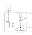
一実施態様は、堆積ツールに結合されたシステムに関係する。堆積ツールは、試料の上に材料の層を形成するように構成することができる。材料の層を試料の上に形成するには堆積ツールを使用する。測定具は、この層を形成する前、形成している間、または形成した後、材料の層の特性を判別するように構成することができる。このシステムは、その試料を支持するように構成されたステージを含むことができる。測定具は、層を形成する前、形成している間、または形成した後、エネルギーを試料の表面に向けるように構成された照明システムを備えることができる。測定具は、さらに、照明システムに結合された検出システムを備えることもできる。検出システムは、層を形成する前、形成している間、または形成した後、試料の表面から伝搬するエネルギーを検出するように構成することができる。測定具はさらに、検出されたエネルギーに対して1つまたは複数の出力信号を生成するように構成することができる。このシステムはさらに、測定具に結合されたプロセッサを備えることもできる。プロセッサは、1つまたは複数の出力信号から層の特性を判別するように構成することができる。プロセッサはさらに、堆積ツールに結合することもできる。プロセッサは、堆積ツールに結合された1つまたは複数の計測器のパラメータを変更するように構成することができる。さらに、プロセッサは、形成された層の判別された特性に対して堆積ツールに結合された計測器のパラメータを変更するように構成することができる。
【0086】
一実施態様では測定具は、非結像スキャタロメータ、スキャタロメータ、分光スキャタロメータ、反射率計、分光反射率計、偏光解析器、分光偏光解析器、明視野撮像デバイス、暗視野撮像デバイス、明視野暗視野撮像デバイス、コヒーレンス・プローブ顕微鏡、干渉顕微鏡、光学プロフィルメータ、またはそれらの任意の組み合わせを備えることができる。このようにして、測定具は単一の測定具としてまたは複数の測定具として機能するように構成することができる。複数の測定具をシステムの単一の測定具に組み込むことができるため、例えば、第1の測定具の光学要素はさらに第2の測定具の光学要素とすることもできる。堆積ツールは、半導体基板の上に層を形成するように構成されたツールを備えることができる。堆積ツールは、化学堆積ツール、物理堆積ツール、原子層堆積ツール、および電気メッキ・ツールを備えることができる。
【0087】
一実施態様では、プロセッサは測定具および/または堆積ツールに結合されたローカル・プロセッサおよびローカル・プロセッサに結合されたリモート・コントローラ・コンピュータを備えることができる。ローカル・プロセッサは、1つまたは複数の出力信号を少なくとも一部処理するように構成することができる。リモート・コントローラ・コンピュータは、プロセッサから少なくとも一部が処理された1つまたは複数の出力信号を受信するように構成することができる。さらに、リモート・コントローラ・コンピュータは、少なくとも一部が処理された1つまたは複数の出力信号から試料上に形成された層の特性を判別するように構成することができる。さらに、リモート・コントローラ・コンピュータは、少なくとも一部が処理された1つまたは複数の出力信号から試料の追加特性を判別するように構成することができる。リモート・コントローラ・コンピュータはさらに、堆積ツールに結合することもできる。このようにして、リモート・コントローラ・コンピュータはさらに、インサイチュー制御手法、フィードバック制御手法、および/またはフィードフォワード制御手法を使用して試料上に形成された層の少なくとも判別された特性に対して堆積ツールに結合された1つまたは複数の計測器のパラメータを変更するように構成することができる。
【0088】
他の実施態様は、試料上に形成された層の特性を評価する方法に関係する。この方法は、堆積ツールを使用して試料上に層を堆積するステップを含むことができる。測定具は、照明システムと検出システムを備えることもできる。さらに、この方法は、照明システムを使用してエネルギーを試料の表面に向けるステップを含むことができる。この方法はさらに、検出システムを使用して試料の表面から伝搬されるエネルギーを検出するステップも含むことができる。この方法はさらに、検出された光に対して1つまたは複数の出力信号を生成するステップを含むことができる。さらに、この方法は、1つまたは複数の出力信号を処理して形成された層の特性を判別するステップを含むことができる。
【0089】
一実施態様では、形成された層の特性を判別するようにプロセッサを構成することができる。さらに、プロセッサは、1つまたは複数の出力信号から試料の他の特性を判別するように構成することができる。他の実施態様では、半導体デバイスをこの方法で製造することができる。例えば、この方法は、半導体基板などの試料の上に半導体デバイスの一部を形成するステップを含むことができる。
【0090】
一実施態様では、1つまたは複数の出力信号を処理して形成された層の特性を判別するステップに、ローカル・プロセッサを使用して1つまたは複数の出力信号を少なくとも一部処理するステップを含めることもできる。ローカル・プロセッサを測定具に結合することができる。1つまたは複数の出力信号を処理するステップがさらに、ローカル・プロセッサからの一部処理された1つまたは複数の出力信号をリモート・コントローラ・コンピュータに送信するステップを含むこともできる。さらに、1つまたは複数の出力信号を処理するステップは、リモート・コントローラ・コンピュータを使用して一部処理された1つまたは複数の出力信号をさらに処理するステップを含むことができる。他の実施態様では、リモート・コントローラ・コンピュータを堆積ツールに結合することができる。このようにして、この方法は試料上に形成された層の少なくとも判別された特性に対してリモート・コントローラ・コンピュータを使用して堆積ツールに結合された1つまたは複数の計測器のパラメータを変更するステップを含むことができる。堆積ツールのパラメータを変更するステップは、インサイチュー制御手法、フィードバック制御手法、および/またはフィードフォワード制御手法を使用するステップを含むことができる。
【0091】
他の実施態様は、堆積ツールおよび測定具を備えるシステムを制御するコンピュータ実装方法に関係する。システムを制御するステップは、測定具、堆積ツール、またはその両方を制御するステップを含むことができる。さらに、測定具は、照明システムと検出システムを備えることができる。測定具はステージに結合することもできる。測定具を制御するステップは、照明システムを制御してエネルギーを試料の表面に向けるステップを含むことができる。さらに、測定具を制御するステップは、検出システムを制御して試料の表面から伝搬するエネルギーを検出するステップを含むことができる。この方法はさらに、検出されたエネルギーに対して1つまたは複数の出力信号を生成するステップを含むこともできる。コンピュータ実装方法は、さらに、1つまたは複数の出力信号を処理して、少なくとも層が形成されるときまたは形成された後の層の特性を判別するステップを含むことができる。さらに、プロセッサは、1つまたは複数の出力信号から試料の他の特性を判別するように構成することができる。
【0092】
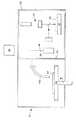
一実施態様は、ビーム・プロフィル偏光解析器に結合されたエッチング・ツールを備えるシステムに関係する。エッチング・ツールは、化学反応および/またはイオン種が試料に向かうように構成することができる。ビーム・プロフィル偏光解析器は、エッチングの間または後に試料のエッチングされた領域の特性を判別するように構成することができる。ビーム・プロフィル偏光解析器は、試料のエッチング中またはエッチング後に極性が知られている光の入射ビームが試料の表面に向かうように構成された照明システムを備えることができる。測定具は、さらに、照明システムに結合された検出システムを備えることもできる。検出システムは、試料のエッチング中またはエッチング後に試料から戻る光を表す1つまたは複数の出力信号を発生するように構成することができる。このシステムはさらに、測定具に結合されたプロセッサを備えることもできる。プロセッサは、1つまたは複数の出力信号から試料のエッチングされた領域の特性を判別するように構成することができる。プロセッサはさらに、エッチング・ツールに結合することもできる。プロセッサは、エッチング・ツールに結合された1つまたは複数の計測器のパラメータを変更することができる。さらに、プロセッサは、エッチングされた層の特性に対してエッチング・ツールに結合された計測器のパラメータを変更するように構成することができる。
【0093】
一実施態様ではシステムは、非結像スキャタロメータ、スキャタロメータ、分光スキャタロメータ、反射率計、分光反射率計、偏光解析器、分光偏光解析器、明視野および/または暗視野撮像デバイス、明視野および/または暗視野非結像デバイス、コヒーレンス・プローブ顕微鏡、干渉顕微鏡、またはそれらの任意の組み合わせを備えることができる。このようにして、システムは単一の測定具としてまたは複数の測定具として機能するように構成することができる。複数の測定具をシステムの単一の測定具に組み込むことができるため、例えば、第1の測定具の光学要素はさらに第2の測定具の光学要素とすることもできる。
【0094】
一実施態様では、プロセッサはビーム・プロフィル偏光解析器および/またはエッチング・ツールに結合されたローカル・プロセッサおよびローカル・プロセッサに結合されたリモート・コントローラ・コンピュータを備えることができる。ローカル・プロセッサは、1つまたは複数の出力信号を少なくとも一部処理するように構成することができる。リモート・コントローラ・コンピュータは、プロセッサから少なくとも一部が処理された1つまたは複数の出力信号を受信するように構成することができる。さらに、リモート・コントローラ・コンピュータは、少なくとも一部が処理された1つまたは複数の出力信号から試料上のエッチングされた領域の特性を判別するように構成することができる。さらに、リモート・コントローラ・コンピュータは、少なくとも一部が処理された1つまたは複数の出力信号から試料の追加特性を判別するように構成することができる。リモート・コントローラ・コンピュータはさらに、エッチング・ツールに結合することもできる。このようにして、リモート・コントローラ・コンピュータはさらに、インサイチュー制御手法、フィードバック制御手法、および/またはフィードフォワード制御手法を使用して試料のエッチングされた領域の少なくとも判別された特性に対してエッチング・ツールに結合された1つまたは複数の計測器のパラメータを変更するように構成することができる。
【0095】
他の実施態様は、ビーム・プロフィル偏光解析器で試料のエッチングされた領域を評価する方法に関係する。この方法は、エッチング・ツールを使用して試料上の層をエッチングするステップを含むことができる。ビーム・プロフィル偏光解析器は、照明システムと検出システムを備えることもできる。さらに、この方法は、照明システムを使用して光を試料の表面に向けるステップも含むことができる。この方法はさらに、検出システムを使用して試料の表面から伝搬される光を検出するステップも含むことができる。この方法はさらに、検出された光に対して1つまたは複数の出力信号を生成するステップを含むことができる。さらに、この方法は、1つまたは複数の出力信号を処理して試料のエッチングされた領域の特性を判別するステップを含むことができる。さらに、この方法は、1つまたは複数の出力信号を処理して、1つまたは複数の出力信号から試料の他の特性を判別するステップを含むことができる。他の実施態様では、半導体デバイスをこの方法で製造することができる。例えば、この方法は、半導体基板などの試料の上に半導体デバイスの一部を形成するステップを含むことができる。
【0096】
一実施態様では、1つまたは複数の出力信号を処理して試料のエッチングされた領域の特性を判別するステップに、ローカル・プロセッサを使用して1つまたは複数の出力信号を少なくとも一部処理するステップを含めることができる。ローカル・プロセッサをビーム・プロフィル偏光解析器に結合することができる。1つまたは複数の出力信号を処理するステップがさらに、ローカル・プロセッサからの一部処理された1つまたは複数の出力信号をリモート・コントローラ・コンピュータに送信するステップを含むこともできる。さらに、1つまたは複数の出力信号を処理するステップは、リモート・コントローラ・コンピュータを使用して一部処理された1つまたは複数の出力信号をさらに処理するステップを含むことができる。他の実施態様では、リモート・コントローラ・コンピュータをエッチング・ツールに結合することができる。このようにして、この方法は試料上に形成された層の少なくとも判別された特性に対してリモート・コントローラ・コンピュータを使用してエッチング・ツールに結合された1つまたは複数の計測器のパラメータを変更するステップを含むことができる。エッチング・ツールのパラメータを変更するステップは、インサイチュー制御手法、フィードバック制御手法、および/またはフィードフォワード制御手法を使用するステップを含むことができる。
【0097】
他の実施態様は、エッチング・ツールおよびビーム・プロフィル偏光解析器を備えるシステムを制御するコンピュータ実装方法に関係する。システムを制御するステップは、ビーム・プロフィル偏光解析器、エッチング・ツール、またはその両方を制御するステップを含むことができる。さらに、ビーム・プロフィル偏光解析器は、照明システムと検出システムを備えることができる。ビーム・プロフィル偏光解析器は、ステージに結合することもできる。ビーム・プロフィル偏光解析器を制御するステップは、照明システムを制御して光を試料の表面に向けるステップを含むことができる。さらに、ビーム・プロフィル偏光解析器を制御するステップは、検出システムを制御して試料の表面からの光を検出するステップを含むことができる。この方法はさらに、検出された光に対して1つまたは複数の出力信号を生成するステップを含むこともできる。コンピュータ実装方法は、さらに、1つまたは複数の出力信号を処理して、エッチング中、領域のエッチング後、またはその両方で、試料のエッチングされた領域の少なくとも1つの特性を判別するステップを含むことができる。さらに、プロセッサは、1つまたは複数の出力信号から試料の他の特性を判別するように構成することができる。
【0098】
一実施態様は、測定具に結合されたイオン注入器を備えるシステムに関係する。測定具は、少なくとも試料のイオン注入領域の特性判別するように構成することができる。測定具は、この試料のイオン注入中または注入後、試料のイオン注入領域の特性を判別するように構成することができる。このシステムは、その試料を支持するように構成されたステージを含むことができる。測定具は、イオン注入中またはイオン注入後、2筋またはそれ以上の光線を定期的に試料の表面に向けるように構成された照明システムを備えることができる。一実施態様では、測定具は、イオン注入中、入射光線を試料に向けることにより試料のある領域を定期的に励起することができる。さらに、測定具は、サンプル光線を試料の励起された表面に向けることができる。測定具は、さらに、照明システムに結合された検出システムを備えることもできる。検出システムは、試料の励起された領域から反射されたサンプル・ビームの強度を測定するように構成することができる。測定具はさらに、測定された強度に対して1つまたは複数の出力信号を生成するように構成することもできる。
【0099】
このシステムはさらに、測定具に結合されたプロセッサを備えることもできる。プロセッサは、1つまたは複数の出力信号からイオン注入領域の特性を判別するように構成することができる。プロセッサはさらに、イオン注入器に結合することもできる。プロセッサは、イオン注入器に結合された1つまたは複数の計測器に結合されたパラメータを変更するように構成することができる。さらに、プロセッサは、イオン注入領域の判別された特性に対してイオン注入器に結合された1つまたは複数の計測器のパラメータを変更するように構成することができる。
【0100】
一実施態様では、測定具は、非結像スキャタロメータ、スキャタロメータ、分光スキャタロメータ、反射率計、分光反射率計、明視野および/または暗視野撮像デバイス、明視野および/または暗視野非結像デバイス、コヒーレンス・プローブ顕微鏡、干渉顕微鏡、光学プロフィルメータ、変調光学反射率計、またはそれらの任意の組み合わせを備えることができる。このようにして、測定具は単一の測定具としてまたは複数の測定具として機能するように構成することができる。複数の測定具をシステムの単一の測定具に組み込むことができるため、例えば、第1の測定具の光学要素はさらに第2の測定具の光学要素とすることもできる。
【0101】
一実施態様では、プロセッサは測定具および/またはイオン注入器に結合されたローカル・プロセッサおよびローカル・プロセッサに結合されたリモート・コントローラ・コンピュータを備えることができる。ローカル・プロセッサは、1つまたは複数の出力信号を少なくとも一部処理するように構成することができる。リモート・コントローラ・コンピュータは、プロセッサから少なくとも一部が処理された1つまたは複数の出力信号を受信するように構成することができる。さらに、リモート・コントローラ・コンピュータは、少なくとも一部が処理された1つまたは複数の出力信号から試料のイオン注入領域の特性を判別するように構成することができる。さらに、リモート・コントローラ・コンピュータは、少なくとも一部が処理された1つまたは複数の出力信号から試料の追加特性を判別するように構成することができる。リモート・コントローラ・コンピュータはさらに、イオン注入器に結合することもできる。このようにして、リモート・コントローラ・コンピュータはさらに、インサイチュー制御手法、フィードバック制御手法、および/またはフィードフォワード制御手法を使用して試料のイオン注入領域の少なくとも判別された特性に対してイオン注入器に結合された1つまたは複数の計測器のパラメータを変更するように構成することができる。
【0102】
他の実施態様は、試料のイオン注入領域を評価する方法に関係する。この方法は、イオン注入器を使用して試料の領域にイオンを注入するステップを含むことができる。測定具は、照明システムと検出システムを備えることができる。さらに、この方法は、イオン注入中またはイオン注入後、入射光線を試料のある領域に向けることにより試料のその領域を定期的に励起するステップを含むことができる。サンプル・ビームはさらに、試料の励起された領域に向けることもできる。この方法はさらに、検出システムを使用して試料の励起された領域から伝搬する光の強度を測定するステップも含むことができる。この方法はさらに、測定された強度に対して1つまたは複数の出力信号を生成するステップを含むことができる。さらに、この方法は、1つまたは複数の出力信号を処理してイオン注入された領域の特性を判別するステップを含むことができる。さらに、この方法は、1つまたは複数の出力信号を処理して、1つまたは複数の出力信号から試料の他の特性を判別するステップを含むことができる。他の実施態様では、半導体デバイスをこの方法で製造することができる。例えば、この方法は、半導体基板などの試料の上に半導体デバイスの一部を形成するステップを含むことができる。
【0103】
一実施態様では、1つまたは複数の出力信号を処理してイオン注入領域の特性を判別するステップに、ローカル・プロセッサを使用して1つまたは複数の出力信号を少なくとも一部処理するステップを含めることができる。ローカル・プロセッサを測定具に結合することができる。1つまたは複数の出力信号を処理するステップがさらに、ローカル・プロセッサからの一部処理された1つまたは複数の出力信号をリモート・コントローラ・コンピュータに送信するステップを含むことができる。さらに、1つまたは複数の出力信号を処理するステップは、リモート・コントローラ・コンピュータを使用して一部処理された1つまたは複数の出力信号をさらに処理するステップを含むことができる。他の実施態様では、リモート・コントローラ・コンピュータをイオン注入器に結合することができる。このようにして、この方法は、試料のイオン注入領域の少なくとも判別された特性に対してリモート・コントローラ・コンピュータを使用してイオン注入器に結合された1つまたは複数の計測器のパラメータを変更するステップを含むことができる。イオン注入器のパラメータを変更するステップは、インサイチュー制御手法、フィードバック制御手法、および/またはフィードフォワード制御手法を使用するステップを含むことができる。
【0104】
他の実施態様は、イオン注入器および測定具を備えるシステムを制御するコンピュータ実装方法に関係する。システムを制御するステップは、測定具、イオン注入器、またはその両方を制御するステップを含むことができる。さらに、測定具は、照明システムと検出システムを備えることもできる。測定具はステージに結合することができる。測定具を制御するステップは、照明システムを制御して光を試料の表面に向けるステップを含むことができる。さらに、測定具を制御するステップは、検出システムを制御して試料の表面からの光を検出するステップを含むことができる。この方法はさらに、検出された光に対して1つまたは複数の出力信号を生成するステップを含むこともできる。コンピュータ実装方法は、さらに、1つまたは複数の出力信号を処理して少なくとも試料のイオン注入領域の特性を判別するステップを含むことができる。さらに、この方法は、1つまたは複数の出力信号から試料の他の特性を判別するステップを含むことができる。
【0105】
一実施態様は、測定具に結合されたプロセス・チャンバを備えるシステムに関係する。プロセス・チャンバは、試料の上に半導体デバイスの一部を製造するように構成することができる。測定具は、試料の上の欠陥の有無を判別するように構成することができる。測定具は、試料上に半導体デバイスの一部を製造する前、製造している間、または製造した後、試料の欠陥の有無を判別するように構成することができる。一実施態様では、測定具は微小欠陥を検出するように構成できる。このシステムは、その試料を支持するように構成されたステージを含む。ステージは、回転するように構成することができる。
【0106】
測定具は、製造前、製造中、または製造した後、エネルギーを試料の表面に向けるように構成された照明システムを備えることができる。さらに、測定具は、ステージが静止している間またはステージが回転している間に試料の表面にエネルギーを向けるように構成することができる。測定具は、さらに、照明システムに結合された検出システムを備えることもできる。検出システムは、試料の表面から伝搬されるエネルギーを検出するように構成することができる。検出システムは、製造前、または製造中、または製造後にエネルギーを検出することができる。検出システムはさらに、ステージが静止または回転している間にエネルギーを検出するように構成することができる。測定具はさらに、検出されたエネルギーに対して1つまたは複数の出力信号を生成するように構成することもできる。
【0107】
このシステムはさらに、測定具に結合されたプロセッサを備えることもできる。プロセッサは、1つまたは複数の出力信号から試料の表面上の欠陥の有無を判別するように構成することができる。プロセッサはさらに、プロセス・チャンバに結合することもできる。プロセッサは、プロセス・チャンバに結合された1つまたは複数の計測器のパラメータを制御することができる。さらに、プロセッサは、試料の表面上の微小欠陥の検出に対してプロセス・チャンバに結合された1つまたは複数の計測器のパラメータを変更するように構成することができる。
【0108】
一実施態様では、測定具は、非結像スキャタロメータ、スキャタロメータ、分光スキャタロメータ、反射率計、分光反射率計、偏光解析器、分光偏光解析器、明視野および/または暗視野撮像デバイス、明視野および/または暗視野非結像デバイス、コヒーレンス・プローブ顕微鏡、干渉顕微鏡、光学プロフィルメータ、またはそれらの任意の組み合わせを備えることもできる。このようにして、測定具は単一の測定具としてまたは複数の測定具として機能するように構成することができる。複数の測定具をシステムの単一の測定具に組み込むことができるため、例えば、第1の測定具の光学要素はさらに第2の測定具の光学要素とすることもできる。
【0109】
一実施態様では、プロセッサは測定具および/またはプロセス・チャンバに結合されたローカル・プロセッサおよびローカル・プロセッサに結合されたリモート・コントローラ・コンピュータを備えることができる。ローカル・プロセッサは、1つまたは複数の出力信号を少なくとも一部処理するように構成することができる。リモート・コントローラ・コンピュータは、ローカル・プロセッサから少なくとも一部が処理された1つまたは複数の出力信号を受信するように構成することができる。さらに、リモート・コントローラ・コンピュータは、少なくとも一部が処理された1つまたは複数の出力信号から試料の欠陥の有無を判別するように構成することができる。さらに、リモート・コントローラ・コンピュータは、少なくとも一部が処理された1つまたは複数の出力信号から試料の追加特性を判別するように構成することができる。リモート・コントローラ・コンピュータはさらに、プロセス・チャンバに結合することもできる。このようにして、リモート・コントローラ・コンピュータはさらに、インサイチュー制御手法、フィードバック制御手法、および/またはフィードフォワード制御手法を使用して試料の欠陥の有無が判別されたことに対応してプロセス・チャンバに結合された1つまたは複数の計測器のパラメータを変更するように構成することができる。
【0110】
他の実施態様は、プロセス・ツールおよび測定具を備えるシステムを使用して試料の表面上の欠陥の有無を評価する方法に関係する。この方法を使用して、試料の上の微小欠陥の有無を検出することができる。この方法は、プロセス・ツールを使用して試料の上に半導体デバイスの一部を製造するステップを含むことができる。測定具は、照明システムと検出システムを備えることもできる。さらに、この方法は、エネルギーを試料の表面に向けるステップも含む。この方法はさらに、検出システムを使用し、試料から伝搬するエネルギーを検出するステップも含むことができる。この方法はさらに、検出されたエネルギーへの応答として1つまたは複数の出力信号を生成するステップを含むこともできる。さらに、この方法は、1つまたは複数の出力信号を処理して、試料の上の欠陥の有無を判別するステップを含むことができる。測定具は、処理前、または処理中、または処理後に欠陥の有無を判別するように構成することができる。試料はさらに、ステージ上に配置することもできる。この方法は、ステージが静止している間またはステージが回転している間に試料の上の欠陥の有無を判別するステップを含むことができる。
【0111】
さらに、この方法は、1つまたは複数の出力信号から試料の他の特性を判別するステップを含むことができる。他の実施態様では、半導体デバイスをこの方法で製造することができる。例えば、この方法は、半導体基板などの試料の上に半導体デバイスの一部を形成するステップも含むことができる。
【0112】
一実施態様では、1つまたは複数の出力信号を処理して試料の欠陥の有無を判別するステップに、ローカル・プロセッサを使用して1つまたは複数の出力信号を少なくとも一部は処理するステップを含めることができる。ローカル・プロセッサを測定具に結合することができる。1つまたは複数の出力信号を処理するステップがさらに、ローカル・プロセッサからの一部処理された1つまたは複数の出力信号をリモート・コントローラ・コンピュータに送信するステップを含むこともできる。さらに、1つまたは複数の出力信号を処理するステップは、リモート・コントローラ・コンピュータを使用して一部処理された1つまたは複数の出力信号をさらに処理するステップを含むことができる。他の実施態様では、リモート・コントローラ・コンピュータをプロセス・ツールに結合することができる。このようにして、この方法は、1つまたは複数の出力信号に対してリモート・コントローラ・コンピュータを使用しプロセス・ツールに結合された1つまたは複数の計測器のパラメータを変更するステップを含むことができる。プロセス・ツールのパラメータを変更するステップは、インサイチュー制御手法、フィードバック制御手法、および/またはフィードフォワード制御手法を使用するステップを含むことができる。
【0113】
他の実施態様は、プロセス・ツールおよび測定具を備えるシステムを制御するコンピュータ実装方法に関係する。システムを制御するステップは、測定具、プロセス・ツール、またはその両方を制御するステップを含むことができる。さらに、測定具は、照明システムと検出システムを備えることができる。測定具はステージに結合することができる。測定具を制御するステップは、照明システムを制御してエネルギーを試料の表面に向けるステップを含むことができる。さらに、測定具を制御するステップは、検出システムを制御して試料の表面から伝搬するエネルギーを検出するステップを含むことができる。この方法はさらに、検出されたエネルギーに対して1つまたは複数の出力信号を生成するステップを含むこともできる。コンピュータによって実装される方法はさらに、処理前、処理中、または処理後、1つまたは複数の出力信号を処理して、試料の欠陥の有無を判別するステップを含むことができる。さらに、プロセッサは、1つまたは複数の出力信号から試料の他の特性を判別するように構成することができる。
【0114】
一実施態様は、試料の複数の表面の上の欠陥の有無を判別するように構成できるシステムに関係する。このシステムは、その試料を支持するように構成されたステージを含む。このシステムはさらに、そのステージに結合された測定具を備えることもできる。ステージは、移動するように構成することができる。測定具は、エネルギーを試料の表面と裏面に向けるように構成された照明システムを備えることができる。照明システムは、ステージが静止している間または移動している間に使用することができる。測定具は、さらに、照明システムに結合された検出システムを備えることもできる。検出システムは、試料の表面と裏面から複数の経路に沿って伝搬するエネルギーを検出するように構成することができる。このシステムはさらに、測定具に結合されたプロセッサを備えることもできる。測定具はさらに、検出された光に対して1つまたは複数の出力信号を生成するように構成することができる。プロセッサは、1つまたは複数の出力信号から試料の表面および裏面の欠陥の有無を判別するように構成することができる。
【0115】
さらに、プロセッサは、1つまたは複数の出力信号から試料の他の特性を判別するように構成することができる。一実施態様では、測定具は、非結像スキャタロメータ、スキャタロメータ、分光スキャタロメータ、反射率計、分光反射率計、偏光解析器、分光偏光解析器、明視野および/または暗視野撮像デバイス、明視野および/または暗視野非結像デバイス、コヒーレンス・プローブ顕微鏡、干渉顕微鏡、光学プロフィルメータ、またはそれらの任意の組み合わせを備えることもできる。このようにして、測定具は単一の測定具としてまたは複数の測定具として機能するように構成することができる。複数の測定具をシステムの単一の測定具に組み込むことができるため、例えば、第1の測定具の光学要素はさらに第2の測定具の光学要素とすることもできる。
【0116】
一実施態様では、プロセッサは測定具に結合されたローカル・プロセッサおよびローカル・プロセッサに結合されたリモート・コントローラ・コンピュータを備えることができる。ローカル・プロセッサは、1つまたは複数の出力信号を少なくとも一部処理するように構成することができる。リモート・コントローラ・コンピュータは、プロセッサから少なくとも一部処理された1つまたは複数の出力信号を受信するように構成することができる。さらに、リモート・コントローラ・コンピュータは、少なくとも一部が処理された1つまたは複数の出力信号から試料の表面および裏面の欠陥の有無を判別するように構成することができる。さらに、リモート・コントローラ・コンピュータは、少なくとも一部が処理された1つまたは複数の出力信号から試料の追加特性を判別するように構成することができる。他の実施態様では、リモート・コントローラ・コンピュータを半導体製造プロセス・ツールなどのプロセス・ツールに結合することができる。このようにして、リモート・コントローラ・コンピュータはさらに、インサイチュー制御手法、フィードバック制御手法、および/またはフィードフォワード制御手法を使用して試料の少なくとも判別された第1または第2の特性に対してプロセス・ツールに結合された1つまたは複数の計測器のパラメータを変更するように構成することができる。
【0117】
他の実施態様は、試料の複数の表面の上の欠陥を判別する方法に関係する。この方法は、ステージに試料を配置するステップを含むことができる。ステージを測定具に結合することができる。測定具は、照明システムと検出システムを備えることができる。さらに、この方法は、照明システムを使用してエネルギーを試料の表面および裏面に向けるステップを含むことができる。この方法はさらに、検出システムを使用して、試料の表面と裏面から複数の経路に沿って伝搬するエネルギーを検出するステップを含むこともできる。この方法はさらに、検出されたエネルギーに対して1つまたは複数の出力信号を生成するステップを含むことができる。さらに、この方法は、1つまたは複数の出力信号を処理して、試料の表面と裏面の欠陥の有無を判別するステップを含むことができる。
【0118】
さらに、プロセッサは、1つまたは複数の出力信号から試料の他の特性を判別するように構成することができる。他の実施態様では、半導体デバイスをこの方法で製造することができる。例えば、この方法は、半導体基板などの試料の上に半導体デバイスの一部を形成するステップを含むことができる。
【0119】
一実施態様では、1つまたは複数の出力信号を処理して試料の複数の表面の欠陥の有無を判別するステップに、ローカル・プロセッサを使用して1つまたは複数の出力信号を少なくとも一部処理するステップを含めることができる。ローカル・プロセッサを測定具に結合することができる。1つまたは複数の出力信号を処理するステップがさらに、ローカル・プロセッサからの一部処理された1つまたは複数の出力信号をリモート・コントローラ・コンピュータに送信するステップを含むこともできる。さらに、1つまたは複数の出力信号を処理するステップは、リモート・コントローラ・コンピュータを使用して一部処理された1つまたは複数の出力信号をさらに処理するステップを含むことができる。他の実施態様では、リモート・コントローラ・コンピュータを半導体製造プロセス・ツールなどのプロセス・ツールに結合することができる。このようにして、この方法は、試料の複数の表面の欠陥の有無を判別した結果に対応してリモート・コントローラ・コンピュータを使用してプロセス・ツールに結合された1つまたは複数の計測器のパラメータを変更するステップを含むことができる。計測器のパラメータを変更するステップは、インサイチュー制御手法、フィードバック制御手法、および/またはフィードフォワード制御手法を使用するステップを含むことができる。
【0120】
他の実施態様は、試料の複数の表面の欠陥を判別するように構成されたシステムを制御するコンピュータ実装方法に関係する。このシステムは測定具を備えることができる。このようにして、システムを制御するステップは、測定具を制御するステップを含むことができる。さらに、測定具は、照明システムと検出システムを備えることができる。測定具はステージに結合することもできる。測定具を制御するステップは、照明システムを制御してエネルギーを試料の表面に向けるステップを含むことができる。さらに、測定具を制御するステップは、検出システムを制御して試料の表面から伝搬するエネルギーを検出するステップを含むことができる。ステージは、移動するように構成することができる。この方法はさらに、分析中に試料が移動するようにしてステージを制御するステップも含むことができる。この方法はさらに、検出されたエネルギーに対して1つまたは複数の出力信号を生成するステップを含むことができる。コンピュータ実装方法は、さらに、1つまたは複数の出力信号を処理して試料の複数の表面の欠陥の有無を判別するステップを含むことができる。
【0121】
一実施態様では、半導体デバイスの生産時に本明細書で説明しているようなシステムのいずれかを使用することができる。半導体デバイスを形成するには、1つまたは複数の半導体処理ステップを使用する。それぞれの処理ステップにおいて、試料に変更が加えられる場合がある。処理ステップの後、半導体デバイスの一部を試料の上に形成することができる。処理ステップの実行前、実行中、または実行後に、試料の少なくとも2つの特性を判別するように構成されたシステムの一ステージ上に試料を配置することができる。システムは、上記の実施態様のいずれかにより構成することができる。
【0122】
第1および第2の特性が判別された後、それらの特性を使用して、半導体デバイスを形成するそれ以降の処理ステップを決定することができる。例えば、このシステムを使用して、半導体プロセスが適切に実行されているかどうかを評価することができる。半導体プロセスが適切に実行されていない場合、システムから得られたデータを使用して、試料をさらに処理するかどうかを決定することができる。他の実施態様では、試料が正しく処理されていないことが検出された場合、その試料を半導体プロセスから取り除く必要があることがあることを示すことができる。上述のような複数の分析システムを使用して、半導体デバイスの処理効率を高めることができる。そのためテストに要する時間を短縮できる。さらに、複数のテストを使用することにより、適切に処理されたことが明らかな試料のみを次の処理ステップに進めるようにできる。このようにして、半導体デバイスの歩留まりを高めることができる。
【0123】
本発明の他の目的および利点は、以下の詳細な説明を読み、添付図面を参照することで明白になるであろう。
【0124】
本発明はさまざまな修正を加えることができ、また他の態様も可能であるが、特定の実施態様を図面の例を用いて示しており、これらについて以下で詳述する。ただし、図面および詳細な説明は本発明を開示されている特定の態様に制限する意図はなく、むしろその反対に、付属の請求項によって定義されているように、発明は本発明の精神と範囲にあるすべての修正、等価物、および代替え物を対象とすることは理解されるであろう。
【0125】
【発明の実施の形態】
そこで図1の図面を参照すると、試料10の表面の実施形態の概略上面図が示されている。試料10は、単結晶シリコン基板、シリコン・ゲルマニウム基板、またはガリウム・ヒ素基板などの基板を含む。さらに、試料10は、半導体デバイスの製造に適していればいずれの基板でもよい。また、試料10は、繰り返し可能なパターン・フィーチャを備える複数のダイス12を備えることができる。それとは別に、試料10は、未使用の半導体のウェーハまたは未処理のウェーハなどパターンが作られていないものでもよい。さらに、試料10は、レチクルの製造に適していると思われる、ガラス基板または実質的に透明な材料から形成された基板を使用することもできる。さらに、試料10は、従来のどのような試料をも含むことができる。
【0126】
さらに、試料10は、基板上に形成した1つまたは複数の層を含んでいてもよい。例えば、基板の上に形成できる層としてこれらに限定はされないが、レジスト、誘電体、および/または導体などがある。レジストは光学的リソグラフィ手法でパターン化されたフォトレジスト材料を含む。ただし、レジストには、電子線レジストやX線レジストなどのレジストがあり、これらは、電子線またはX線リソグラフィ手法でそれぞれパターン化される。適切な誘電体の例としては、二酸化珪素、窒化ケイ素、酸窒化ケイ素、および窒化チタンなどがある。さらに、適切な導体の例としては、これらに限定はされないがアルミニウム、多結晶シリコン、および銅がある。さらに、試料には、ウェーハなどの基板上に形成されたトランジスタなどの半導体デバイスを含めることもできる。
【0127】
図2aおよび2bは、試料を支持するように構成されているステージ24の一実施形態の概略上面図を示している。ステージは、真空チャックまたは静電チャックであってよい。この方法で、試料をステージ上の適切な位置にしっかり保持することができる。さらに、ステージは、モーター駆動平行移動ステージ、ロボット・ウェーハ・ハンドラ、または当業界で知られているその他の適切な機械式デバイスとすることができる。一実施形態では、システムはステージに結合された測定具26を備えることができる。したがって、ステージは、測定具に対して試料に相対的な運動を伝えるように構成することができる。一例としては、試料の測定具に対する相対運動を直線方向になるようにステージを構成することができる。ステージの相対運動により、測定具のエネルギー源からの入射エネルギー・ビームは試料の表面を横切るが、その際に、光が試料の表面に当たる入射角度に実質的な変化は生じない。ここで使用しているように「測定具」という用語は、広く測定器具、検査器具、または測定および検査の組み合わせ器具を指す。
【0128】
図2aおよび2bに示されているように、ステージ24は、試料が測定具26に対して複数の方向に向けられるようにベクトル28による指示に従って時計回りおよび反時計回りに回転できるように構成することができる。このようなステージを使用すると、測定または検査中に測定具に対して試料を揃えるように試料の向きを修正することもできる。さらに、ステージ24は、回転と直線移動を同時にできるように構成することもできる。試料を測定具に揃える方法の例が、Eylonによる米国特許出願第5682242号、Eylonによる米国特許出願第5867590号、およびFinarovによる米国特許出願第6038029号に説明されており、参照により本明細書に完全に規定されているかのように取り込まれる。
【0129】
一実施形態では、ステージ24はさらに、z軸に沿って移動し試料と測定具26の間の距離を変えるように構成することもできる。例えば、試料と測定具との間の距離を変更することで、測定具のエネルギー源からのエネルギー・ビームの焦点が試料の表面に確実に結ばれるようにできる。システムの焦点を定める例が、Finarovによる米国特許出願第5604344号、およびFeldmanらによる米国特許出願第6124924号に説明されており、参照により本明細書に完全に規定されているかのように取り込まれる。荷電粒子ビームを試料に集束させる例は、Pearlらによる欧州特許出願番号EP 1 081 741 A2に説明されており、参照により本明細書に完全に規定されているかのように取り込まれる。
【0130】
図2aに示されているように、ステージ24を、測定具26に対して移動するように構成することができ、測定具を、そのステージに対して移動するように構成することもできる。例えば、測定具26をベクトル29によって示されている方向に沿って直線移動するように構成し、ステージ24を回転移動するように構成することができる。そのようにして、ステージが回転しているときに測定具のエネルギー源からの入射エネルギー・ビームをステージの半径方向に横切らせることができる。
【0131】
図2bに示されているように、測定具30を、ステージ24に対してある位置に相対的に静止するように構成することができる。測定具30内の音響光学偏向器(「AOD」)などの偏向器(ただしこれだけには限られない)を含む器具(図に示されていない)を、ステージに対して入射ビームの位置を直線的に変えるように構成することができる。AODの例は、AllenらによるPCT出願番号WO 01/14925 A1に説明されており、参照により本明細書に完全に規定されているかのように取り込まれる。このようにして、入射ビームをステージが回転しているときにステージの半径方向へ横切らせることができる。さらに、このような器具を使用してステージに対する入射ビームの位置を変更することにより、試料の表面に形成されたパターンとともに測定具のレジストリを維持できる。測定具のエネルギー源からの入射エネルギー・ビームを試料の表面を横切らせ、その際に、エネルギーのビームが試料の表面に当たる入射角度に実質的な変化が生じないように器具を構成することができる。
【0132】
他の実施形態では、測定具30は照明システムなどの複数のエネルギー源と複数の検出システムを備えることができる。複数の照明システムと複数の検出システムを2つの直線的アレイに配列することができる。照明システムと検出システムは、各照明システムが検出システムの1つに結合されるようにすることができる。したがって、測定具30は、直線的撮像デバイスとして構成できる。このようにして、測定具を、試料の表面の位置を実質的に同時にまたは順次測定または検査するように構成することができる。さらに、測定具を、ステージが回転している間に実質的に同時に試料上の複数の位置で測定するように構成することができる。さらに、ステージと測定具を、実質的に連続的または間欠的に移動するように構成できる。例えば、システムを移動−取得−測定システムとして構成するようにステージと測定具を間欠的に移動させることもできる。
【0133】
試料の測定または検査位置を制御し、変更するために上記のように構成された測定具とステージは、現在使用されているシステムと比較していくつかの利点がある。例えば、試料上の複数の位置を検査するように構成されている現在使用されているシステムは、静止測定具と2つの別々の方向に横へ移動するように構成されたステージを含む。それとは別に、現在使用されているシステムは、第1の方向の2つの鏡の位置および第2の方向の2つの鏡の位置を変更することにより、静止ステージおよび試料に入射したエネルギー・ビームの位置を変更するように構成された測定具を含む。このようなシステムの例は、Finarovによる米国特許出願第5517312号、およびFinarovによる米国特許出願第5764365号に説明されており、参照により本明細書に完全に規定されているかのように取り込まれる。他のシステムは、回転するように構成されたステージと放射状に移動するように構成されたレーザー光源を備えることができる。このようなシステムは、パターン化された試料を測定または検査するのには適していないと思われる。現在使用されているシステムの他の例は、Holmesによる米国特許出願第5943122号に説明されており、参照により本明細書に完全に規定されているかのように取り込まれる。
【0134】
ウェーハなどの試料の横方向寸法が300mmになると、検査または測定時に試料を直線的に移動させることは、標準的な半導体製造設備に必要なスペースの関係上、実用的でないと思われる。さらに、このように試料を移動させることは、このようなツールに対するスペースを比較的大きく確保するコストが高くつくため、かなり費用がかかる可能性がある。したがって、上の実施形態で説明されているように構成されているシステムは、試料を直線移動することなく試料の表面全体を検査または測定するように構成するとよい。
【0135】
図3は、試料の少なくとも2つの特性を判別するように構成されたシステム32の一実施形態の概略側面図を示している。システム32は、照明システム36および検出システム38を備える測定具34を備えることができる。照明システム36は、ステージ42の上に配置されている試料40の表面に光が当たるように構成されている。ステージ42は、上の実施形態で説明されているように構成されている。検出システム38は、照明システム36に結合でき、また試料の表面からの光を検出するように構成することができる。例えば、検出システム38、照明システム36、および追加の光学系コンポーネントを、試料40の表面から送られてくるスペクトル反射光または散乱光を検出システムにより検出できるように配列することができる。
【0136】
照明システム36はエネルギー源44を備えることができる。エネルギー源44は、単色光を放射するように構成されている。例えば、適切な単色光源をガスレーザーまたは固体レーザー・ダイオードとすることができる。それとは別に、エネルギー源を、紫外線、可視光、赤外線、X線、ガンマ線、マイクロ波、または無線周波を含む複数の波長の電磁放射を放射するように構成することもできる。さらに、エネルギー源を、電子、陽子、中性子、イオン、または分子のビームなど他のエネルギー源を放射するように構成することもできる。例えば、熱電界放射源は通常、電子源として使用される。
【0137】
検出システム38は検出器46を備えることができる。検出器46は、光検出器、複数セル光検出器、干渉計、リニア・センサ・アレイなどのフォトダイオード・アレイ、従来の分光光度計、位置検知検出器、光電子増倍管、アバランシェ・フォトダイオード、電荷結合素子(「CCD」)カメラ、時間遅延積分(「TDI」)カメラ、ビデオ・カメラ、パターン認識デバイス、および撮像システムなどの光感知デバイスを備えることができる。さらに、検出器は、ショットキー固体障壁検出器などの固体検出器であってもよい。
【0138】
さらに、測定具34は光学系コンポーネントをいくつでも追加することができる(図に示されていない)。適切な光学系コンポーネントとしては、これらに限定されないが、ビーム・スプリッタまたはダイクロイック・ミラー、4分の1波長板、直線偏光器および円偏光器などの偏光器、回転偏光器、回転検光子、コリメータ、集光レンズ、追加レンズ、折り畳み式鏡、部分的透過型ミラー、スペクトルまたは偏光フィルタ、空間フィルタ、リフレクト、デフレクタ、およびモジュレータのフィルタなどがある。追加光学系コンポーネントはそれぞれ、照明システムまたは検出システム内に結合または配置することができる。さらに、測定具は、磁気集光レンズ、磁気対物レンズ、静電偏向システム、ビーム開口絞り、およびウィーン・フィルタを含む電磁デバイス(図に示されていない)を多数追加することができる。
【0139】
照明システム、検出システム、および追加光学および電磁コンポーネントの配置は、例えば、試料の少なくとも2つの特性を判別するために使用する手法により異なることがある。照明システム、検出システム、および追加光学系および電磁コンポーネントの配置もまた、判別される資料の特性により異なる。例えば、図3に示されているように、測定具34は照明システム36内に配置または結合されている光学系コンポーネント48を備えることができる。光学系コンポーネント48には、これらに限定されないが偏光器、スペクトルまたは偏光フィルタ、および4分の1波長板などがある。さらに、測定具34はビーム・スプリッタ50および光学系コンポーネント52を備えることができる。光学系コンポーネント52は、検出システム38内に配置または結合することができる。光学系コンポーネント52には、これらに限定されないが、4分の1波長板、コリメータ、集光レンズなどがある。
【0140】
図4〜7には、システム32の測定具34の他の実施形態が示されている。後述のように、図3〜7に示されている実施形態のそれぞれにおいて同様に構成することができるシステム32の要素は、同じ参照文字で示されている。例えば、エネルギー源44は、図3〜7に示されているそれぞれの実施形態において同じように構成できる。図4に示されているように、測定具34は複数のエネルギー源44を備えることができる。それぞれのエネルギー源は、実質的に似た種類のエネルギーまたは異なる種類のエネルギーを放射するように構成することができる。例えば、複数のエネルギー源44は本明細書で説明しているいずれかの光源を備えることができる。光源を、広帯域光を放射するように構成することができる。それとは別に、光源を2つ用意し異なる種類の光を放射させるようにすることができる。例えば、一方の光源を、単一波長の光を放射するように構成し、他方の光源を、広帯域光を放射するように構成することができる。さらに、図4に示されているように、エネルギー源は試料40の表面の実質的に同じ位置にエネルギー・ビームを向けるように構成することができる。それとは別に、図5に示されているように、複数のエネルギー源44を、試料40の表面の実質的に異なる位置にエネルギーを向けるように構成することができる。例えば、図5に示されているように、複数のエネルギー源を、試料40の表面の横方向に間隔をあけて並ぶ位置にエネルギー・ビームを向けるように構成することができる。また図5に示されている複数のエネルギー源を、上述のように構成することもできる。
【0141】
図4に示されているように、測定具は複数のエネルギー源44に結合された検出器46を備えることができる。このようにして、鏡面反射光および散乱光などの試料40の表面から来る異なる種類のエネルギーを検出する検出器を構成できるように検出器46を複数のエネルギー源に対して配置することができる。検出器はさらに、実質的に同時に、試料の表面から来る異なる種類のエネルギーを検出するように構成することもできる。例えば、検出器は、フォトダイオードのアレイを備えることができる。フォトダイオードのアレイの第1の部分を、試料の表面から来る複数の光源の1つから入射する光のみを検出するように構成し、フォトダイオードのアレイの第2の部分を、試料の表面から来る複数の光源のうちの別の光源から入射する光のみを検出するように構成することができる。実質的に同時に試料の表面から来る複数の光源のそれぞれから入射する光を検出するように検出器を構成することができる。それとは別に、複数のエネルギー源は、エネルギーが試料の表面に間欠的に向けられるように構成することができる。試料の表面から来る複数のエネルギー源のそれぞれから入射するエネルギーを間欠的に検出するように検出器を構成することもできる。
【0142】
図5に示されているように、測定具34は複数の検出器46を備えることができる。複数の検出器のそれぞれを、複数のエネルギー源44の1つに結合することができる。このようにして、検出器が試料40の表面から来るエネルギー源の1つから入射するエネルギーを検出するように、エネルギー源の1つに対してそれぞれの検出器46を配置することができる。例えば、試料の表面から散乱された光を検出するように第1の光源に対して検出器の1つを配置することができる。一例としては、散乱光は、暗視野経路に沿って来る暗視野光を含む。明視野経路に沿って来る明視野光などの試料の表面から鏡面反射された光を検出するように複数の検出器のうちの第2の検出器を第2の光源に対して配置することができる。上の実施形態で説明されているように複数の検出器を構成することができる。例えば、複数の検出器は2つの異なる検出器または2つの同じ種類の検出器を含むことができる。例えば、第1の検出器は、従来の分光光度計として構成し、第2の検出器は、クォッド・セル(四分割セル)検出器として構成することができる。それとは別に、両方の検出器をフォトダイオードのアレイとして構成することもできる。
【0143】
図4に示されているように、測定具34はさらに複数の光学系コンポーネント48を備えることもできる。例えば、光学系コンポーネント48を複数のエネルギー源44のそれぞれに結合することができる。一例としては、光学系コンポーネントの第1のものを偏光器として構成し、光学系コンポーネントの第2のものを集光レンズとして構成することができる。それとは別に、図5に示されているように、測定具34は複数のエネルギー源44のそれぞれに結合された1つの光学系コンポーネント48を備えることができる。光学系コンポーネント48のそれぞれは、本明細書で説明しているように構成することができる。さらに、図5に示されているように、測定具34は複数のエネルギー源の1つに結合されたビーム・スプリッタ50などの光学系コンポーネントを備えることもできる。例えば、ビーム・スプリッタ50は光源から発せられる光の経路に沿って配置される。ビーム・スプリッタ50は光源から光を試料の表面へ送り、試料の表面からの光を反射するように構成させることができる。ビーム・スプリッタは、試料の表面からの光を反射させ、その反射された光が検出器46に向かうように構成させることができる。さらに、ビーム・スプリッタを、複数の光源のそれぞれから発せられる光の経路に沿って配置することができる。図4に示されているように、光学系コンポーネント52は、検出器46に結合することができ、このコンポーネントを例えば、4分の1波長板、コリメータ、および集光レンズとして構成することができる。光学系コンポーネント52をさらに、本明細書で説明しているように構成することができる。複数の光学系コンポーネント52はさらに、検出器のそれぞれに結合される。しかし、光学系コンポーネントのそれぞれの位置および構成は、以下で詳述するようなシステムによって決定される試料の特性によって異なる。
【0144】
図6および7は、システム32の他の実施形態の概略側面図を示す。これらの図に示されているように、測定具34は単一のエネルギー源44を備えている。さらに、測定具34は複数の検出器46を備えている。これらの検出器は、本明細書で説明しているようなデバイスであればどれでもよい。複数の検出器46のそれぞれを、エネルギー源44に関して異なる角度で配置することができる。例えば、図6に示されているように、暗視野経路に沿って来る暗視野光を検出するように検出器の1つを構成することができる。明視野経路に沿って来る明視野光を検出するように第2の検出器を構成することができる。それとは別に、図7に示されているように、複数の検出器のそれぞれを鏡面反射光を検出するように構成することができる。複数の検出器を似たような形で、例えばフォトダイオード・アレイとして構成することができる。それとは別に、複数の検出器を従来の分光光度計およびクォッド・セル検出器などの異なる検出器として構成することができる。
【0145】
さらに、照明システムを、異なる種類のエネルギーが試料の表面に変化するインターバルで向けられるように構成することができる。例えば、エネルギー源は、1種類の光を放射する構成である。図7に示されているように、光学系コンポーネント48をエネルギー源44に結合することができる。光学系コンポーネント48は、さらに、エネルギー源44によって放射される光を変化するインターバルで変えるように構成することもできる。例えば、光学系コンポーネント48は、エネルギー源44によって変化するインターバルで放射される光の経路内で回転される複数のスペクトルおよび/または偏光フィルタとして、またはフィルタに結合されたコントローラによって制御される液晶ディスプレイ(「LCD」)・フィルタとして構成することができる。コントローラは、LCDフィルタの透過、反射、および/または偏光特性を変化するインターバルで変えるように構成することができる。LCDフィルタの特性を変化させることにより、エネルギー源から放射された光のスペクトル特性または偏光状態を変えることができる。さらに、複数の検出器はそれぞれ、試料の表面から来る異なる種類の光を検出するのに適したものでよい。したがって、測定具は、試料の実質的に異なる光学的特性を変化するインターバルで測定するように構成することができる。このようにして、試料の表面に向かうエネルギーと試料の表面から戻るエネルギーが、例えば、システムを使用して測定する試料の特性に応じて変化するように測定具34を構成することができる。
【0146】
一実施形態では、図3〜7に示されているように、システム32は測定具34に結合されたプロセッサ54を備えることができる。このプロセッサは、測定具検出器で発生する1つまたは複数の出力信号を受信するように構成することができる。1つまたは複数の出力信号は、試料から戻り検出されたエネルギーを表すことができる。この1つまたは複数の出力信号はアナログ信号でもデジタル信号でもよい。プロセッサは、検出器で発生した1つまたは複数の出力信号から試料の少なくとも第1の特性と第2の特性を判別することができる。第1の特性は、試料40の限界寸法を含み、第2の特性は、試料40のオーバーレイ・ミスレジストレーションを含むことができる。例えば、測定具は、これらに限定されないが、スキャタロメータ、非結像スキャタロメータ、分光スキャタロメータ、反射率計、分光反射率計、楕円偏光計、分光楕円偏光計、ビーム・プロフィル楕円偏光計、明視野撮像デバイス、暗視野撮像デバイス、明視野暗視野撮像デバイス、明視野非結像デバイス、暗視野非結像デバイス、明視野暗視野非結像デバイス、コヒーレンス・プローブ顕微鏡、干渉顕微鏡、光学プロフィルメータ、またはそれらの任意の組み合わせを備えることができる。このようにして、システムは単一の測定具または複数の測定具として構成することができる。
【0147】
複数の測定具を単一のシステムに組み込むことができるため、例えば、第1の測定具の光学要素はさらに第2の測定具の光学要素として使用することもできる。さらに、複数の測定具を共通ステージ、共通ハンドラ、および共通プロセッサに結合することができる。本明細書で説明しているハンドラは、試料を共通ステージに配置し、共通ステージまたは他のハンドラから試料を取り除くように構成された機械デバイスを備えることができる。さらに、このシステムは、連続してあるいはほぼ同時に、試料の限界寸法およびオーバーレイ・ミスレジストレーションを判別できるように構成されている。この方法では、このようなシステムは半導体業界で現在使用しているシステムに比べて、コスト、時間、およびスペースの面で効率が優れていると思われる。
【0148】
図8は、試料の一実施形態の概略側面図を示している。図8に示されているように、複数のフィーチャ56を試料60の上面58に形成する。例えば、試料の上面に形成されたフィーチャは、局所的相互接続部、ゲート電極と誘電体側壁スペーサからなるゲート構造、コンタクト・ホール、ビアなどである。しかし、これら複数のフィーチャは、試料内に形成することもできる。例えば、試料内に形成されたフィーチャは、半導体基板およびトレンチ内のフィールド酸化膜領域などの分離構造である。限界寸法には、試料60上のフィーチャ56の幅62などの試料の上面に実質的に平行な方向で定義されている機能の横方向寸法を含めることができる。したがって、限界寸法は、一般的に、ゲートまたは相互接続部の幅または穴もしくはビアの直径など断面で見たときのフィーチャの横方向寸法として定義することができる。フィーチャの限界寸法には、さらに、試料60上のフィーチャ56の高さ64などの試料の上面に実質的に垂直な方向で定義されているフィーチャの横方向寸法も含めることができる。
【0149】
さらに、限界寸法は、フィーチャの側壁角度も含むことができる。「側壁角度」は、一般的に、試料の上面に関するフィーチャの側面(または横)の角度として定義することができる。このようにして、フィーチャの高さに対して幅が実質的に一様なフィーチャはその側壁角度66が約90度となる。フィーチャの高さに対して幅が実質的に一様な半導体デバイスなどの試料のフィーチャを比較的近い位置にまとめて形成し、半導体デバイスのデバイス密度を高めることができる。さらに、このようなデバイスの電気的特性は比較的予測可能であり、また実質的に一様であると思われる。フィーチャの高さに対して傾斜したプロフィルを持つかまたは幅が実質的に一様でないフィーチャはその側壁角度68が約90度未満となる。傾斜したプロフィルは、フィーチャの上に層を形成する場合に望ましい。例えば、傾斜したプロフィルでは、フィーチャの上に形成された層内の空隙の発生を低減することができる。
【0150】
オーバーレイ・ミスレジストレーションは、一般に、試料の第2のレベルのフィーチャの横の位置に関する試料の第1のレベルのフィーチャの横の位置のずれの尺度として定義することができる。第1のレベルは、第2のレベルの上に形成することができる。例えば、オーバーレイ・ミスレジストレーションは、半導体デバイスの複数のレベルのフィーチャのアラインメントを表している。理想的には、オーバーレイ・ミスレジストレーションは、試料の第1のレベル上のフィーチャを試料の第2のレベル上のフィーチャに完全に揃えられるようにほぼ0であるのが好ましい。例えば、オーバーレイ・ミスレジストレーションが大きいと、試料の第1および第2のレベル上に電気的フィーチャの接触が生じることがあり望ましくない。この方法では、このようなミスアラインメントの大きな試料上に形成された半導体デバイスに多数の開回路または短絡回路が生じ、デバイスの不具合の基になる。
【0151】
試料のオーバーレイ・ミスレジストレーションの程度は、例えば、リソグラフィ・プロセスの性能特性によって異なる。リソグラフィ・プロセスの実行中、レチクルつまりマスクは試料の第1のレベルに配置されているレジストの上に配置される。レチクルは、レジストに転写できる、パターンが構成された実質的に透明な領域と実質的に不透明な領域を持つ。レチクルは、試料上のアラインメントマークの位置を検出するように構成された露光ツールにより試料の上に配置することができる。この場合、オーバーレイ・ミスレジストレーションは、アラインメントマークを検出し、試料に対してレチクルの位置を変える露光ツールの性能上の制限によって生じることがある。
【0152】
図9は、複数の測定具を備えるシステム70の一実施形態の概略上面図を示している。測定具のそれぞれは、本明細書で説明しているように構成される。例えば、各測定具を試料の少なくとも1つの特性を判別するように構成する。さらに、各測定具を試料の異なる特性を判別するように構成することもできる。そこで、システム70を、試料の少なくとも4つの特性を判別するように構成する。例えば、測定具72を、試料の限界寸法を判別するように構成する。さらに、第1の横方向で試料のオーバーレイ・ミスレジストレーションを判別するように測定具74を構成する。測定具76については、第2の横方向で試料のオーバーレイ・ミスレジストレーションを判別するように構成する。第1の横方向は、第2の横方向に実質的に直交する方向である。さらに、測定具78をパターン認識デバイスとして構成することができる。したがって、システム70を、試料の少なくとも4つの特性を同時にまたは順次判別するように構成することができる。さらに、本明細書で説明している測定具をそれぞれ、試料の任意の特性を判別するように構成することができる。
【0153】
図10は、試料の少なくとも2つの特性を判別するように構成されたシステム80の一実施形態の概略側面図を示している。例えば、システム80は、試料の少なくとも限界寸法を判別するように構成されている。したがって、システム80を上の実施形態で説明されているようにシステム70に含めることができる。システム80は広帯域光源82を備えている。「広帯域光」という用語は、一般的に、2つまたはそれ以上の異なる周波数成分を含む周波数振幅スペクトルを持つ放射光を指すのに用いられる。広帯域周波数振幅スペクトルには、190nm程度から1700nm程度までのさまざまな波長範囲が含まれる。しかし、波長の範囲は、たとえば光源能力、照射対象のサンプル、および判別される特性により広い場合も狭い場合もある。例えば、可視光線と紫外線を含む光線を放射するように構成されたキセノンアーク・ランプを広帯域光源として使用することができる。
【0154】
システム80は、光源82から放射された光を試料85の表面に当てるように構成されたビーム・スプリッタ84を備えることもできる。ビーム・スプリッタは、連続広帯域スペクトルの光を出力するように構成できるビーム・スプリッタ鏡として構成されている。システム80は、ビーム・スプリッタ84から来る光の焦点を試料85の表面に定めるように構成されたレンズ86を備える。試料85の表面から戻る光は、ビーム・スプリッタ84を通り、回折格子88に届く。回折格子は、試料の表面から戻された光を分散するように構成されている。分散された光は、検出器アレイ90などの分光計に向けることができる。この検出器アレイは、リニア・フォトダイオード・アレイを含むことができる。光は分光計に入ると回折格子により分散させられ、その結果得られるサンプル・ビームの一次回折回折光線がリニア・フォトダイオード・アレイに集まる。分光反射率計の例が、Goldらによる米国特許出願第4999014号、およびNortonらによる米国特許出願第5747813号に説明されており、参照により本明細書に完全に規定されているかのように取り込まれる。
【0155】
したがって、フォトダイオード・アレイで、試料の表面から戻る光の反射スペクトル92を測定することができる。相対的反射スペクトルを求めるには、各波長の反射スペクトルの戻された光の強度を各波長の相対的基準強度で割ればよい。相対的反射スペクトルを使用して、ウェーハ上のさまざまな膜の厚さを測定することができる。さらに、単一波長の反射率および膜の屈折率も、相対的反射スペクトルから求めることができる。さらに、モード展開(「MMME」)モデル94によるモデル手法を使用して、さまざまな反射スペクトルのライブラリ96を生成することができる。MMMEモデルは、パラメータ空間内の各格子から理論的回折光の「指紋」を計算するために使用できる厳密な回折モデルである。しかし、他のモデルも、厳密カップリング導波管分析(rigorous coupling waveguide analysis:「RCWA」)モデルなど(これに限定されない)の理論的回折光を計算するのに使用することもできる。測定された反射スペクトル92をライブラリ96内のさまざまな反射スペクトルに当てはめることができる。本明細書で説明しているように、当てはめたデータ97を使用して、試料の表面上のフィーチャの横方向寸法、高さ、および側壁角度などの限界寸法95を求めることができる。モデル作成手法の例は、XuらによるPCT出願番号WO99/45340に説明されており、参照により本明細書に完全に規定されているかのように取り込まれる。
【0156】
図11aおよび11bは、試料の限界寸法などの特性を判別するように構成された測定具98の一実施形態の他の概略側面図である。測定具を上述のシステム80に結合することができる。測定具98は光ファイバ光源100を備えている。光ファイバ光源は、光を放射し、コリメート鏡102に向けるように構成されている。コリメート鏡102は、光ファイバ光源によって放射された光の経路を変えて、経路106に沿って実質的に一方向に試料104の表面に向かって行くように構成されている。光ファイバ光原100から放射された光はさらに、反射鏡108にも向けられる。反射鏡108は、光ファイバ光源によって放射された光を基準分光計110に向けるように構成されている。基準分光計110は、光ファイバ光源によって放射された光の強度を測定するように構成されている。さらに、基準分光計110は、測定された光の強度に対して1つまたは複数の出力信号を発生するように構成することもできる。そこで、基準分光計110によって生成される信号を使用して、光ファイバ光源によって放射された光の強度の変動を監視することができる。
【0157】
測定具98はさらに、偏光器112を備えることもできる。偏光器112は、光の経路106に対して45度の角度に向けることができる。偏光器112は、光の偏光状態を変化させ試料の表面に向かって行く光を直線偏光または回転偏光させるように構成されている。測定具98はさらに、光の経路106に沿って配置された光ピストン114を備えることもできる。この光ピストンは、試料の表面に向かって行く光の経路の方向を変える。例えば、測定具の光ピストンは試料の複数の位置を測定するために測定具の一部115が試料に対して移動するように構成されている。このようにして、試料の表面に光が当たる入射角度が実質的に変わらないようにしながら、経路106に沿って来る光を試料の表面を横断させるようにすることできる。
【0158】
測定具はさらに、アポダイザ116を備えることもできる。アポダイザ116は、比較的透過度の高い領域と実質的に不透明な領域が交互に並ぶ二次元パターンを持つ。この交互パターンは、アポダイズ関数などのような局所的平均透過率関数を持つ。したがって、アポダイザは、測定具の集光分解能を高めるために試料の光の当たる領域の横の部分を減らすように構成されている。また、測定具は、経路106に沿って来る光が試料の表面に当たるように構成された複数の鏡118を備えている。さらに、測定具は、光が試料の表面に向かうように構成された反射対物レンズ120を備えている。例えば、適切な反射対物レンズの開口数(「NA」)を約0.1とし、光を高い入射角度で試料の表面に向けることができる。
【0159】
試料の表面から戻ってきた光は、対物レンズ120と鏡の1つにより検光子122へと反射される。検光子122は、試料の表面から戻った光を光の偏光状態に基づき2つの反射光に分割するように構成されている。例えば、検光子112は、偏光状態が実質的に異なる2つの別々の光線を発生するように構成されている。図11bに示されているように、測定具はオートフォーカス・センサ124を備えている。オートフォーカス・センサ124は、試料に入射したスポットの焦点が合っている像を受け取るように構成された分割フォトダイオード検出器を備えている。焦点が合っているスポットの像は、検光子122と鏡118の間の光経路に沿って配置されたビーム・スプリッタ125から得られる。例えば、試料104から戻った光の一部をオートフォーカス・センサに向けるようにビーム・スプリッタを構成している。オートフォーカス・センサ124は、像の強度を測定し、測定された強度を表す信号をプロセッサに送信するように構成された2つのフォトダイオードを備えている。オートフォーカス・センサの出力を焦点信号と呼ぶことができる。焦点信号はサンプル位置の関数である。プロセッサは、焦点信号の最大値の位置を使用して、測定具に対する試料の焦点位置を判別するように構成されている。
【0160】
また、測定具は試料の表面から戻ってきた光が分光計128に導くように構成された鏡126を備えている。分光計128は、ある波長帯域にわたる反射率のs成分とp成分の強さを測定するように構成されている。「s成分」という用語は、一般に、電界が反射されたビームの入射平面に実質的に垂直になっている偏光の成分を説明するために使用される。「p成分」という用語は、一般に、電界が反射されたビームの入射平面内にある偏光の成分を説明するために使用される。本明細書で説明しているように、測定した反射スペクトルを使用して、試料の表面上のフィーチャの限界寸法、高さ、および側壁角度を求めることができる。例えば、相対的反射スペクトルを求めるには、分光計128で測定した各波長の戻ってきた光の強度を測定具基準分光計110により測定した各波長の相対的基準強度で割る。この相対反射スペクトルをデータの論理モデルに当てはめて、限界寸法、高さ、および側壁角度を求めることができる。
【0161】
一実施形態では、図9に示されているように、システム70の測定具74および測定具76は、コヒーレンス・プローブ顕微鏡、干渉顕微鏡、または光学プロフィルメータとして構成されている。例えば、コヒーレンス・プローブ顕微鏡は、特別に改造されたLinnik顕微鏡とビデオ・カメラ、試料搬送ステージ、およびデータ処理電子回路を組み合わせて構成されている。それとは別に、Fringes of Equal Chromatic Order (“FECO”)、Nomarski偏光干渉計、差動干渉コントラスト(「DIC」)、Tolansky繰返し反射干渉法、およびMichelson、Fizeau、およびMirauに基づく2ビーム・ベースの干渉法などの他の干渉光プロファイリング顕微鏡および手法をシステムに合わせて改造することができる。この測定具では、広帯域または比較的狭い帯域のいずれかの光を使用して、試料の表面に対して異なる軸位置(迎角)で撮像した複数の干渉像を発生させることができる。干渉像は、一連の像平面を構成する。これらの平面内のデータは、ビデオ信号強度に対する加法的変換により変換することができる。変換された像データを使用することで、変換された平面内のピクセルごとに物体波と参照波との間の絶対相互可干渉性を測定することができる。光経路長を変えたときに輝度が絶対相互可干渉に比例する合成像を形成することができる。
【0162】
一実施形態では、干渉顕微鏡として構成された測定具は、入射光線を放射するように構成されたキセノン・ランプなどのエネルギー源を備えている。適切なエネルギー源はさらに、レーザーによって出力される光などのコヒーレント光を放射するように構成された光源を備えている。測定具は、さらに、入射光線を試料の表面に向けるように構成された追加光学コンポーネントを備えている。適切な追加光学コンポーネントは、集光レンズ、フィルタ、ディフューザ、開口絞り、および視野絞りを備えている。追加光学コンポーネントはさらに、ビーム・スプリッタ、顕微鏡対物レンズ、部分的透過鏡を備えている。
【0163】
入射光線の第1の部分を試料の表面に向けることができるように測定具内に光学コンポーネントを配置することができる。さらに、入射光線の第2の部分を基準鏡に向けることができるように測定具内に光学コンポーネントを配置することができる。例えば、試料の表面にサンプル光線を向ける前に入射光線を部分的透過鏡に通すことにより入射光線の第2の部分を発生させることができる。試料の表面から反射された光を基準鏡から反射された光と組み合わせることができる。一実施形態では、検出システムは従来の干渉計を備えている。反射された入射光線は基準光線と組み合わさって、干渉計に入射させられる。試料の表面から反射された光入射光線と基準鏡から反射された基準光線は位相が一致していないので、この組み合わせた光線内に干渉パターンが発生する。組み合わせたビームの干渉パターンの強度変化は、干渉計で検出できる。
【0164】
干渉計は、組み合わせたビームの干渉パターンの検出された強度変化に対応する信号を発生するように構成されている。発生した信号を測定面に関する表面情報が得られるように処理することができる。測定具はさらに、光入射光線の制御を補助するスポッター顕微鏡を備えている。スポッター顕微鏡を電子回路を介して測定具に結合し、入射光線を一部制御するようにできる。使用する干渉顕微鏡および方法の例は、Davidsonらによる米国特許出願第5112129号、Mazorらによる第5438313号、Ausschnittらによる第5712707号、Ausschnittらによる第5757507号、Ausschnittらによる第5805290号、Ausschnittらによる第5914784号、Bareketによる第6023338号で説明されており、すべて、参照により本明細書に完全に規定されているかのように取り込まれる。
【0165】
他の実施形態では、光学プロフィルメータとして構成されている測定具を使用して試料の表面の高さを測定することができる。本明細書で説明している光学プロフィルメータは、光散乱法、光切断法、およびさまざまな干渉光プロファイリング手法を使用するようになっている。光学プロフィルメータは、2筋のビーム経路の光の干渉を測定するようになっている。試料の表面の高さが変化すると、光線経路長の1つが変化し、それにより干渉パターンが変化する。そこで、測定された干渉パターンを使用して、試料の表面の高さを判別することができる。Nomarski偏光干渉計は、光学プロフィルメータとして使用するのに適している。
【0166】
一実施形態では、光学プロフィルメータは、入射光線を放射するように構成されたタングステン・ハロゲン白熱灯などの光源を備えている。この光源は、赤外線、紫外線、および/または可視光線などさまざまな波長の光を放射するようになっている。この光源を、さらに、レーザーから出力される光などのコヒーレント光を放射するように構成することもできる。光学プロフィルメータはさらに、光を試料の表面に向けるように構成された光学コンポーネントを備えている。このような光学コンポーネントは、本明細書で説明しているような光学コンポーネントのいずれかを備えている。光学プロフィルメータはさらに、電磁放射光を位相シフトするように構成された回転検光子、電荷結合素子(「CCD」)カメラ、フレーム取込み器、および電子処理回路を備えている。フレーム取込み器は、CCDカメラなどの検出器から信号を受信し、その信号を変換する(つまり、像をデジタル化する)ようになっているデバイスである。4分の1波長板およびスペクトル・フィルタも、光学プロフィルメータに含めることができる。偏光器やNomarskiプリズムは、対物レンズの分解能限界よりも小さい距離だけ試料の表面上の横方向にオフセットしている実質的に直角に偏光している2つのビームで試料が照らされるように構成されている。試料から戻ってきた後の光線は、Nomarskiプリズムで再結合させることができる。
【0167】
一実施形態では、光学プロフィルメータは従来の干渉計を備えている。再結合された光線の干渉パターンは干渉計で検出できる。検出された干渉パターンを使用して、試料の表面プロフィルを判別することができる。光学プロフィルメータの例は、Samsavarらによる米国特許出願第5955661号に説明されており、参照により本明細書に完全に規定されているかのように取り込まれる。オーバーレイ・ミスレジストレーションを判別するように構成された測定具の例は、Nikoonahadらによる「Metrology System Using Optical Phase」という表題の2000年8月14日に出願された米国特許出願第09/639495号に説明されており、参照により本明細書に完全に規定されているかのように取り込まれる。
【0168】
一実施形態では、測定具78は、パターン認識デバイスとして構成できる。測定具78は、可視光線および紫外線などの広帯域の光を放射するように構成されたランプなどの光源を備えている。この測定具はさらに、光源によって放射された光の一部を対物レンズに向けサンプル光線を形成するように形成されたビーム分割鏡を備えている。対物レンズとしては、複数の倍率を持つ反射対物レンズがある。例えば、この対物レンズとしては、15倍率Schwartzchild設計全反射対物レンズ、4倍率Nikon CFN Plan Apochromat、1倍率UV透過対物レンズがある。これら3つの対物レンズは、3つの対物レンズのうちの1つがサンプル光線の経路内に入るように回転するタレットに取り付けることができる。対物レンズは、サンプル光線が試料の表面に向かうように構成されている。
【0169】
試料の表面から戻ってくる光は対物レンズとビーム分割鏡を通り、測定具のサンプル板に入る。サンプル板は、開口が板を通して形成されている反射石英ガラス板でよい。試料の表面から戻ってくる光は、一部、サンプル板から比較的短い焦点距離アクロマートを通って反射される。戻ってくる光は、折り畳み式の鏡からビーム・スプリッタ・キューブへ反射される。ビーム・スプリッタ・キューブは、戻ってきた光の一部がペンタプリズムに向かうように構成されている。ペンタプリズムは、戻ってくる光の一部を反射するようになっている。戻ってきた光の反射された部分も、比較的焦点距離の長いアクロマートおよびフィルタなどの測定具78の追加光学コンポーネントを通ることができる。戻ってきた光の反射された部分は、戻ってきた光がビデオ・カメラを向くように構成された折り畳み式鏡に当たる。さらに、ビデオ・カメラは、試料の表面の非反転像を発生するように構成されている。パターン認識デバイスの例は、Piwonka−Corleらによる米国特許出願第5910842号に説明されており、参照により本明細書に完全に規定されているかのように取り込まれる。
【0170】
他の実施形態では、測定具は、非結像スキャタロメータ、スキャタロメータ、または分光スキャタロメータを採用することができる。スキャタロメトリは、構造体から散乱された光の角度分解測定および特性を必要とする手法である。例えば、反復パターン・フィーチャなど周期的パターンで試料上に配置されている構造だと、入射光は異なる順序に散乱または回折される。構造から回折された光パターンを「指紋」または「シグネチャ」として使用し、反復可能パターン・フィーチャの特性を識別することができる。例えば、回折光パターンを分析し、周期、幅、ステップ高さ、側壁角度、基礎層の厚さ、および試料上のフィーチャのプロフィルなどの試料の表面上の反復可能パターン・フィーチャの特性を判別することができる。
【0171】
スキャタロメータは、単一波長の光が試料の表面に向かうように構成された光源を備えている。例えば、この光源は、ガスレーザーまたは固体レーザー・ダイオードを備えている。それとは別に、光源は、複数の波長の光が試料の表面に向かうように構成されている。したがって、スキャタロメータは、分光スキャタロメータとして構成できる。一例としては、光源は広帯域放射光を放射するように構成されている。適切な広帯域光源は、放射された光の偏光状態をランダム化するように構成された光ファイバ・ケーブルに結合された白色光源を備え、実質的に一様な入射光線を発生することができる。光ファイバ・ケーブルから放射された光は、測定具内に配置された複数の光コンポーネントを通過する。例えば、光ファイバ・ケーブルから放射された光は入射光線のスポット・サイズを制限するように構成されたスリット開口を通過できる。スポット・サイズは、一般に、入射光線によって照らされる試料の表面面積として定義することができる。光ファイバ・ケーブルから放射された光は、集光レンズを通過することができる。さらに、光ファイバ・ケーブルから放射された光は、偏光状態が知られている入射光線を生成するように構成された偏光器を通過することができる。偏光状態が知られている入射光線は試料の表面に向かうことができる。
【0172】
スキャタロメータは、さらに、分光計を含む検出システムを備えている。分光計は、試料の表面から散乱されたさまざまな波長の光の強度を測定するように構成されている。一実施形態では、0次回折強度を測定することができる。ただしいくつかの反復可能パターン・フィーチャについては、高次の回折強度の測定も可能である。分光計によって生じた異なる波長における0次および/またはそれ以上の次数の回折強度に対応する信号を分光計に結合されているプロセッサに送ることができる。プロセッサは、試料の表面の構造のシグネチャを判別するように構成されている。さらに、プロセッサは、試料の表面上の反復可能パターン・フィーチャの特性を判別するように構成されている。例えば、判別されたシグネチャとデータベースに記録されているシグネチャとを比較するようにプロセッサを構成することもできる。データベースのシグネチャは、モデル作成により特性および/またはシグネチャが判別されて知られている試料で実験的に決定されたシグネチャを含むことができる。反復可能パターン・フィーチャの特性には、基礎層の周期幅、ステップ高さ、側壁角度、厚さ、および試料上のフィーチャのプロフィルがある。
【0173】
上述のように、スキャタロメータは照明システムに結合されたに偏光器を備えている。偏光器は、さらに、第1の偏光状態の照明システムの光源により放射された光を透過し、第2の偏光状態の光源により放射された光を反射するように構成されている。さらに、スキャタロメータは、検出システムに結合された検光子を備えている。この検光子は、実質的に偏光器と同じ偏光状態の光を透過するようになっている。例えば、検光子は、第1の偏光状態の試料の表面から散乱された光を透過するように構成されている。他の実施形態では、スキャタロメータは照明システムと検出システムに結合されたステージを備えている。ステージは、本明細書で説明したように構成されている。このようにして、実質的に異なる特性が試料の表面上に形成される反復可能パターン・フィーチャの特性を順次または同時に判別することができる。測定具の例は、XuらによるPCT出願番号WO99/45340に説明されており、参照により本明細書に完全に規定されているかのように取り込まれる。試料から散乱された光を測定するように構成された測定具の他の例が、Leslieらによる米国特許出願第6081325号、Vaez−Iravaniらによる米国特許出願第6201601号、およびNikoonahadらによる米国特許出願第6215551号に説明されており、参照により本明細書に完全に規定されているかのように取り込まれる。
【0174】
スキャタロメータなどの測定具は、撮像デバイスまたは非結像デバイスのいずれかであってよい。撮像デバイスでは、試料の表面から散乱された光をレンズにより捕捉することができる。このレンズではさらに、反射光でエンコードされている空間情報を保存することができる(例えば、光強度の空間分布)。さらに、スキャタロメータは電荷結合素子(「CCD」)カメラ、CMOSフォトダイオード、またはフォトゲート・カメラなどの光検出デバイスのアレイとして構成されている検出器を備えている。それとは別に、非結像デバイスでは、光源から出た光は、試料の表面上の比較的小さな領域に向けられる。光電子増倍管、フォトダイオード、またはアバランシェ・フォトダイオードなどの検出器で、散乱または回折された光を検出し、検出された光の積分した光強度に比例する信号を発生する。
【0175】
他の実施形態では、測定具は、明視野撮像デバイス、暗視野撮像デバイス、または明視野暗視野撮像デバイスとして構成されている。「明視野」とは一般に、試料からの鏡面反射光を集めるように構成された集束幾何学的構造を指す。明視野集束幾何学的構造は、任意の入射角度を持つことができるが、通常は、試料平面に対し法線となる入射の角度を持つ。明視野撮像デバイスは、光を試料の表面に向けるように構成された光源を備えている。光源はさらに、試料の表面の実質的に連続する照明を実現するように構成されてもよい。例えば、光源は蛍光灯であってよい。連続照明もまた、光拡散要素に結合された1列に並んだ点光源により実現できる。このような光源は、本明細書で説明しているような光源であればどのようなものをも含む。
【0176】
明視野撮像デバイスはさらに、試料の表面から明視野経路に沿って来る明視野光を集めるように構成された明視野撮像システムを備えている。明視野光は、試料の表面から鏡面反射された光を含む。明視野撮像システムは、スリット鏡および結像レンズなどの光学コンポーネントを備えている。スリット鏡は、試料の表面から明視野経路に沿って来る明視野光が結像レンズに向けるように構成されている。結像レンズは、スリット鏡から反射された明視野光を受け取るように構成されている。例えば、結像レンズは、明視野光の光学収差を減らし、結像視野の縁の強度減少の効果を低減するように構成された固定レンズでよい。結像レンズを、レンズを通過する光が結像レンズの後ろに配置されている光検出デバイスに集束するように構成することもできる。光検出デバイスとしては、これらに限定しないが、8000PNダイオード要素ライン・スキャン・センサ、CCDカメラ、TDIカメラ、またはその他の適切な種類のデバイスを使用できる。
【0177】
光検出デバイスの1つまたは複数の出力信号をイメージ・コンピュータに送信して処理することができる。イメージ・コンピュータは、一般的にマシン・ビジョン業界で使用している並列処理システムとすることができる。イメージ・コンピュータはさらに、明視野撮像デバイスを制御し、データ処理機能を実行するように構成されたホスト・コンピュータに結合することもできる。例えば、データ処理機能としては、試料上の複数の位置に光を向けることにより発生する光検出デバイスの複数の出力信号を比較することで試料の表面上の欠陥の有無を判別する機能がある。試料上の複数の位置としては、例えば、図1に示されているような試料の2つのダイスがを含めることができる。
【0178】
「暗視野」とは一般に、試料からの散乱光のみを集めるように構成された集束幾何学的構造を指す。「二重暗視野」とは一般に、急角度の斜行照明を使用する検査幾何学的構造および入射平面を外れている集光角度を指す。このような配置には、すれすれの照明角度および表面散乱を抑制するすれすれの集光角度が含むことができる。このような抑制は、入射波と反射波が干渉することで表面近くの暗フリンジ(Weinerフリンジとも呼ばれる)が生じるため発生する。暗視野撮像デバイスは、本明細書で説明しているような光源であればどのようなものをも含むことができる。二重暗視野デバイスは、撮像デバイスまたは非結像デバイスのいずれかである。
【0179】
暗視野撮像デバイスはさらに、試料の表面から暗視野経路に沿って来る暗視野光を集めるように構成された暗視野撮像システムを備えている。本明細書で説明している暗視野撮像システムは、光学コンポーネント、イメージ・コンピュータ、およびホスト・コンピュータを含む。本明細書で説明している方法で、試料の表面の欠陥の有無を試料の暗視野像から判別することができる。暗視野撮像用に構成された検査システムの例は、AlmogyによるPCT出願番号WO 99/31490に説明されており、参照により本明細書に完全に規定されているかのように取り込まれる。
【0180】
さらに、測定具は、1つまたは複数の光源を含む、明視野光源および暗視野光源を備えている。光源はそれぞれ、試料の表面に関して異なる入射角度で配置することができる。それとは別に、各光源を試料の表面に対して同じ入射角度で配置することもできる。測定具はさらに、上で説明したように、明視野および暗視野撮像システムを備えている。例えば、測定具は1つまたは複数の撮像システムを備えている。撮像システムはそれぞれ、試料の表面に対して異なる入射角度で配置することができる。それとは別に、各撮像システムを試料の表面に対して同じ入射角度で配置することもできる。したがって、測定具は、明視野および暗視野撮像デバイスとして動作するように構成されている。各撮像システムは、上で説明したように構成されている同じイメージ・コンピュータに結合させることができる。さらに、イメージ・コンピュータはホスト・コンピュータに結合させることができ、これも上で説明したように構成されている。ホスト・コンピュータも、測定具の明視野コンポーネントおよび暗視野コンポーネントの両方を制御するように構成することもできる。
【0181】
しかし、明視野、暗視野、および明視野暗視野デバイスは、非結像デバイスとして構成することもできる。例えば、上で説明した検出器は、光電子増倍管、フォトダイオード、またはアバランシェ・フォトダイオードで置き換えることができる。このような検出器は、明視野光および/または暗視野光の積算光強度に比例する信号を出力するようになっている。
【0182】
図12は、使用中試料の少なくとも2つの特性を判別するように構成されたシステム32の他の実施形態の概略側面図を示している。後述のように、図3〜7および12に示されている実施形態のそれぞれにおいて同様に構成できるシステム32の要素は、同じ参照文字で示されている。例えば、ステージ42は図3〜7および12に示されている実施形態のそれぞれにおいて同様に構成されている。
【0183】
ここで使用しているように、用語「表面」および「裏面」は一般的に、試料の両側を指す。例えば、ウェーハなど試料の「表面」または「上面」という用語を使用して、半導体デバイスが形成されるウェーハ面を指すことができる。同様に、ウェーハなど試料の「裏面」または「下面」という用語を使用して、実質的に半導体デバイスがないウェーハ面を指すことができる。
【0184】
システム32は、試料40を支えるように構成されたステージ42を備えている。図12に示されているように、ステージ42は試料を支持するために試料の外側横縁に近い試料の裏面に接触する。例えば、このステージは、試料を支持するように構成されたロボット・ウェーハ・ハンドラを備えている。他の実施形態では、ステージの上面は、試料の裏面の表面積よりも小さい表面積を持つように構成されている。このようにして、ステージ42は試料の中心つまり内側表面領域に近い試料の裏面と接触し試料を支える。一例としては、ステージは、真空チャックまたは静電チャックを備えている。このようなステージは、半導体製造プロセス・ツールなどのプロセス・ツールのプロセス・チャンバ内に配置し、半導体製造工程段階などの工程段階で試料を支えるように構成されている。このようなステージはさらに、本明細書で説明しているように他の測定具に取り入れることもできる。
【0185】
システム32は、ステージに結合された測定具を備えている。この測定具は複数のエネルギー源44を備えている。複数のエネルギー源44の第1のものは、エネルギーが試料40の表面40aに向けられるように構成されている。図12に示されているように、2つの検出器46aおよび46bを複数のエネルギー源の第1のものに結合できる。これら2つの検出器は、第1のエネルギー源に関して異なる角度に配置することができる。このようにして、検出器はそれぞれ、試料40の表面40aから来る異なる種類のエネルギーを検出するように構成されている。例えば、検出器46bは、試料40の表面から来る暗視野光を検出するように構成されている。さらに、検出器46aは、試料40の表面から来る明視野光を検出するように構成されている。しかし、他の実施形態では、単一の検出器、つまり検出器46aまたは検出器46bのいずれかを測定具に装備し、第1のエネルギー源に結合することができる。コンポーネント48などの追加コンポーネントも第1のエネルギー源に結合できる。例えば、コンポーネント48は、本明細書で説明しているような光コンポーネントであればどのようなものでもよい。
【0186】
測定具はさらに、コンポーネント50を備えている。例えば、コンポーネント50は、光源から光を試料40に向けて送り、試料40から来る光を検出器46aに向けて反射するように構成されたビーム・スプリッタを備えている。測定具は、さらに、検出器46aに結合された追加コンポーネント52を備えている。コンポーネント52は、上の実施形態で説明したように構成される。さらに、このようなコンポーネントは検出器46bに結合することもできる。しかし、コンポーネントのそれぞれの位置および構成は、例えば、システムによって測定される試料の特性によって異なってよい。
【0187】
一実施形態では、複数のエネルギー源44の第2のものは、エネルギーが試料40の裏面40bに向けられるように構成されている。測定具は、さらに、第2のエネルギー源に結合された検出器46cを備えている。さらに、複数の検出器を第2のエネルギー源に結合することもできる。検出器46cを第2のエネルギー源に関して、試料40の裏面40bから来る特定の種類のエネルギーを検出できるように配置することができる。例えば、検出器46cを第2のエネルギー源に関して、試料40の裏面40bから暗視野経路に沿って来る暗視野光を検出できるように配置することができる。追加コンポーネント48を第2のエネルギー源に結合することもできる。コンポーネント48は、本明細書で説明しているような光コンポーネントであればどのようなものでもよい。さらに、システム32はプロセッサ54を備えている。プロセッサ54は、図12に示されているように、検出器46a、46b、および46cのそれぞれに結合することができる。このプロセッサは、本明細書で説明したように構成されている。
【0188】
したがって、上の実施形態によれば、システム32は、試料の少なくとも2つの表面上の少なくとも2つの特性を判別するように構成されている。例えば、システム32は、試料の表面の欠陥の有無を判別するように構成されている。さらに、システム32は、試料の裏面の欠陥の有無を判別するように構成されている。さらに、このシステムは、試料の追加表面の欠陥の有無を判別するように構成されている。例えば、このシステムは、試料の表面、裏面、および縁の欠陥の有無を判別するように構成されている。ここで使用しているように、試料の「縁」という用語は一般的に、試料の表面および裏面の実質的に法線方向となる試料の外側の横の表面を指す。さらに、このシステムは、試料の複数の表面の欠陥の有無を同時に判別するように構成されている。
【0189】
他の実施形態では、さらに、試料の1つまたは複数の表面の欠陥の個数、試料の1つまたは複数の表面の欠陥の位置、および/または試料の1つまたは複数の表面の欠陥の種類を、順次または実質的に同時に判別するようにシステムを構成することもできる。例えば、プロセッサは、測定具によって検出されたエネルギーから、試料の1つまたは複数の表面上の欠陥の個数、位置、および/または種類を判別するように構成されている。試料の表面に存在する欠陥の種類を判別する方法の例は、Berezinらによる米国特許出願第5831865号に説明されており、参照により本明細書に完全に規定されているかのように取り込まれる。試料の表面に存在する欠陥の種類を判別する方法の他の例は、RavidらによるWO 99/67626、Ben PorathらによるWO 00/03234号、およびHansenによるWO 00/26646号に説明されており、参照により本明細書に完全に規定されているかのように取り込まれる。
【0190】
さらに、プロセッサ54は、試料の少なくとも3つの特性を判別するように構成されている。これら3つの特性には、試料の限界寸法、試料のオーバーレイ・ミスレジストレーション、および試料の1つまたは複数の表面上の欠陥の有無、個数、位置、および/または種類が含まれる。このようにして、このシステムは、試料の限界寸法、試料のオーバーレイ・ミスレジストレーション、および試料の1つまたは複数の表面上の欠陥の有無、個数、位置、および/または種類を順次または実質的に同時に判別するように構成されている。
【0191】
このシステムは、試料の1つまたは複数の表面上の微小な欠陥および/または目立つ欠陥を順次にまたは実質的に同時に判別するように構成されている。目立つ欠陥および微小な欠陥を判別するように構成されたシステムの例は、Sandlandらによる米国特許出願第4644172号に説明されており、参照により本明細書に完全に規定されているかのように取り込まれる。Sandlandによって説明されているようなマクロ−ミクロ光学系を、本明細書で説明しているように、測定具に組み込み、これを1ステージに結合することができる。ステージは、本明細書で説明したように構成されている。このようにして、Sandlandのマクロ−ミクロ光学系は、試料の1つまたは複数の表面上の微小な欠陥および/または目立つ欠陥を実質的に同時に判別するように構成されている。さらに、Sandlandのマクロ−ミクロ光学系は、試料が単一ステージに配置されている間に試料の1つまたは複数の表面上の微小な欠陥および/または目立つ欠陥を順次判別するように構成されている。それとは別に、測定具は、Addiegoによる、参照により本明細書に完全に規定されているかのように取り込まれる米国特許出願第5917588号に説明されているような光学コンポーネントを備えることができる。例えば、本明細書で説明しているように、測定具は、Addiegoによって説明されているような開発後検査(「ADI」)マクロ検査システムのマクロ光学系に結合されたSandlandによって説明されているようなミクロ光学系を備えている。
【0192】
微小な欠陥は、通常、横方向の寸法が約25μm未満である。目立つ欠陥は、横方向の寸法が約25μmを超えるような歩留まりを制限する大規模な欠陥を含む。このような大規模な欠陥には、レジストの浮き上がり、薄いレジスト、フォトレジストの余分な被覆、不完全または欠損のあるレジストなどのレジストや現像装置の問題があり、原因は、滴下ノズルの詰まりや、不正な工程順序、現像装置または水のスポットである。目立つ欠陥の例として他に、ピンぼけ(「ホット・スポット」)の領域、傾斜したレチクルや間違って選択されたレチクルなどのレチクルの誤り、ひっかき傷、レジストの現像過剰または不足などのパターン完全性の問題、粒子や繊維などの汚染、不均一または完全なエッジ・ビード除去(「EBR」)などがある。「ホット・スポット」という用語は、例えば、露光ツールの焦点深度の制限、露光ツールの不具合、露光時に試料の平面になっていない表面、試料の裏面または支持デバイスの表面の異物、または設計上の制約によって生じるフォトレジスト露光欠陥を指す。例えば、試料の裏面または支持デバイスの表面に異物がついていると試料が変形してしまう可能性がある。試料がこのように変形すると、露光プロセス実行中に焦面が不均一になるおそれがある。さらに、このような不均一な焦面は試料上に望ましくないまたは欠損パターン・フィーチャ変化として現れてよい。
【0193】
上述の欠陥はそれぞれ、暗視野または明視野照明のいずれかのもとでフィーチャ的なシグネチャを持つことがある。例えば、ひっかき傷は暗視野照明のもとでは暗色背景に明るい線として現れる。しかし、フォトレジストが余分であったりフォトレジストの被覆が不完全だと、明視野照明の下で薄膜干渉効果が発生する。さらに、大きなピンボケ欠陥は暗視野照明の下で横方向に近いダイスによって生じるパターンと比較してぼんやりとしたまたは明るいパターンとして現れる。レジストの過剰露光または不足露光によって生じる欠陥、線幅の大きな変動、大きな粒子、コメット、縞、欠損フォトレジスト、現像不足または現像過剰レジスト、および、現像装置スポットなどの他の欠陥は明視野暗視野照明の下でフィーチャ的なシグネチャを持つ。
【0194】
図1に示されているように、試料10の表面には複数の欠陥がありえる。試料10の表面にある欠陥14はレジスト被覆が不完全であるというものである。例えば、不完全なレジスト被覆は、コーティング・ツールの故障やレジスト滴下システムの故障によって生じることがある。試料10の表面にある欠陥16は表面のひっかき傷であろう。試料10の表面にある欠陥18はレジストの層の不均一な領域である。例えば、レジストのこのような不均一な領域は、コーティング・ツールの故障や塗布後焼き付けツールの故障によって生じることがある。試料10の表面にある欠陥20はホット・スポットである。さらに、試料10の表面にある欠陥22は不均一なエッジ・ビード除去(「EBR」)であろう。上述の欠陥はそれぞれ、試料10の表面のどのような場所にも存在することができる。さらに、各欠陥もまたいくつでも、試料の表面に存在する可能性がある。
【0195】
試料の表面の欠陥の有無を判別する方法とシステムの他の例は、Levyらによる米国特許第4247203号、Levyらによる米国特許第4347001号、Galbraithによる米国特許第4378159号、Josephらによる米国特許第4448532号、Wihlらによる米国特許第4532650号、Broadbent,Jr.et al.による米国特許第4555798号、Sandlandらによる米国特許第4556317号、Levyらによる米国特許第4579455号、Galbraithによる米国特許第4601576号、Sandlandらによる米国特許第4618938号、Wihlによる米国特許第4633504号、Pecenによる米国特許第4641967号、Sandlandらによる米国特許第4644172号、Saadatらによる米国特許第4766324号、Spechtらによる米国特許第4805123号、Davidsonによる米国特許第4818110号、Tsaiらによる米国特許第4845558号、Chadwickらによる米国特許第4877326号、Vaughtらによる米国特許第4898471号、Danielsonらによる米国特許第4926489号、Neukermansらによる米国特許第5076692 号、Jannらによる米国特許第5189481号、Vaughtらによる米国特許第5264912号、Wellsらによる米国特許第5355212号、Evansらによる米国特許第5537669号、Emeryらによる米国特許第5563702号、Grossによる米国特許第5565979号、Wihlらによる米国特許第5572598号、Johnsonらによる米国特許第5604585号、Emeryらによる米国特許第5737072号、Vaez−Iravaniによる米国特許第5798829号、Nikoonahadによる米国特許第5633747号、Tsaiらによる米国特許第5822055号、Nikoonahadらによる米国特許第5825482号、Jordan,IIIらによる米国特許第5864394号、Nikoonahadらによる米国特許第5883710号、Addiegoによる米国特許第5917588号、Rosengausらによる米国特許第6020214号、Wihlらによる米国特許第6052478号、Chuangらによる米国特許第6064517号、Tsaiらによる米国特許第6078386号、Leslieらによる米国特許第6081325号、Elyasafらによる米国特許第6175645号、Alumotらによる米国特許第6178257号、Almogyによる米国特許第6122046号、およびNikoonahadらによる米国特許第6215551号に示されており、すべて参照により本明細書に完全に規定されているかのように取り込まれる。欠陥検査方法および装置の他の例は、ElyasafらによるPCT出願WO 99/38002号、ReinhronらによるWO 00/68673号、LehanによるWO 00/70332号、FeuerbaumらによるWO 01/03145号、およびAlmogyらによるWO 01/13098号に示されており、参照により本明細書に完全に規定されているかのように取り込まれる。欠陥検査方法および装置の他の例は、Dotanによる欧州特許出願EP 0 993 019 A2号、DotanによるEP 1 061 358 A2号、Ben−PorathによるEP 1 061 571 A2号、HarveyらによるEP 1 069 609 A2号、KarpolらによるEP 1 081 489 A2号、PearlらによるEP 1 081 742 A2号、およびKenanらによるEP 1 093 017 A2号に示されており、参照により本明細書に完全に規定されているかのように取り込まれる。したがって、上述の実施形態はさらに、本明細書で参照により取り込まれる特許のすべてにおいて説明されているシステムおよび方法のフィーチャを含むことができる。
【0196】
他の実施形態では、本明細書で説明しているようなシステムを、試料の平坦性を測定するように構成することもできる。「平坦性」とは、一般に、試料の表面積に対する試料の上面の領域形状特性の平均として定義することができる。例えば、領域形状特性として、これらに限定されないが、試料の上面の粗さおよび試料上に配置された層の上面の平面一様性などがある。層の上面の粗さおよび平面一様性は、例えば、測定前に試料に対し実行するプロセスによって異なり、半導体製造の例では、エッチング、堆積、メッキ、化学機械研磨、またはコーティングを含むことができる。
【0197】
本明細書で説明しているプロセッサは、検出されたエネルギーから、試料の少なくとも3つの特性を判別するように構成されている。これら3つの特性は、試料の限界寸法、試料のオーバーレイ・ミスレジストレーション、および試料の平坦さなどである。さらに、プロセスは、検出されたエネルギーから試料の4つの特性を判別するように構成されている。これら4つの特性には、試料の限界寸法、試料のオーバーレイ・ミスレジストレーション、および試料の平坦さ、試料の欠陥の有無、個数、位置、および/または種類を含めることができる。したがって、このシステムは、試料の限界寸法、試料のオーバーレイ・ミスレジストレーション、平坦性測定、および/または試料の表面上の欠陥の有無、個数、位置、および/または種類を順次または実質的に同時に判別するようになっている。
【0198】
図13は、半導体製造プロセス・ツールに結合されたシステム32の一実施形態の概略上面図を示している。例えば、このシステムをリソグラフィ・ツール130に結合することができる。リソグラフィ・ツールは一般にリソグラフィ・トラックまたはクラスタ・ツールと呼ばれ、複数のプロセス・チャンバ132、144、146、148、150、154、および156を含むことができる。プロセス・チャンバの個数と構成は、例えば、リソグラフィ・ツールで処理されるウェーハの種類によって異なることができる。リソグラフィ・ツールおよびプロセスの例は、Ushijimaによる米国特許第5393624号、Shiraishiらによる米国特許出願第5401316号、Hobbsらによる米国特許第5516608号、Yoshiokaらによる米国特許第5968691号、およびPhanらによる米国特許第5985497号に説明されており、参照により本明細書に完全に規定されているかのように取り込まれる。リソグラフィ・ツール130は、露光チャンバ134を備えている露光ツールに結合することができる。プロセス・チャンバの第1の部分は、レジストの露光の前にリソグラフィ・プロセスの1ステップを実行するようになっている。プロセス・チャンバの第2の部分は、レジストの露光の後にリソグラフィ・プロセスの1ステップを実行するように構成されている。
【0199】
一実施形態では、リソグラフィ・ツール130は少なくとも1つのロボット・ウェーハ・ハンドラ136を備えている。ロボット・ウェーハ・ハンドラ136は、第1のプロセス・チャンバから第2のプロセス・チャンバへ試料を移動させるように構成されている。例えば、ロボット・ウェーハ・ハンドラはベクトル138によって一般的に示される方向に沿って移動するように構成されている。さらに、ロボット・ウェーハ・ハンドラは、ベクトル140によって示される方向に回転することで試料を、リソグラフィ・ツールの第1の側に配置されている第1のプロセス・チャンバからリソグラフィ・ツールの第2の側に配置されている第2のプロセス・チャンバに移動させるように構成することもできる。第1の側および第2の側は、リソグラフィ・ツールの実質的な両側に配置することができる。ロボット・ウェーハ・ハンドラをさらに、リソグラフィ・ツール130から露光ツールの露光チャンバ134に試料を移動させるように構成することもできる。このようにして、ロボット・ウェーハ・ハンドラは、試料を一連のプロセス・チャンバに順次通して、試料に対してリソグラフィ・プロセスを実行することができる。
【0200】
ロボット・ウェーハ・ハンドラをさらに、リソグラフィ・ツールのロード・チャンバ142内に配置されているカセット141からリソグラフィ・ツールのプロセス・チャンバに試料139を移動させるように構成することもできる。このカセットは、リソグラフィ・プロセスの実行中に処理することができる試料を多数保持するように構成されている。例えば、カセットは正面開放統一ポッド(「FOUP」)でよい。ロボット・ウェーハ・ハンドラは、表面処理チャンバ144などのプロセス・チャンバ内に試料を配置するようになっている。表面処理チャンバは、試料の表面上でヘキサメチルジシラザン(「HMDS」)などの粘着促進剤を形成するように構成されている。HMDSは、約80℃から約180℃の温度で堆積する。表面処理プロセスの後、ロボット・ウェーハ・ハンドラは、表面処理チャンバ144から試料を取り出し、その試料を冷却チャンバ146に入れるように構成されている。そこで、試料の温度は後の処理に適した温度に下げる(例えば、20℃から25℃程度)ように冷却チャンバ146を構成している。
【0201】
他の実施形態では、反射防止膜を試料の表面に形成することができる。反射防止膜を試料に形成するには、スピン・コーティングの後に塗布後焼き付けプロセスを実行する。反射防止膜の塗布後焼き付けプロセスでは一般に、コーティングされた試料を170℃から230℃程度で加熱する必要があるため、この塗布後焼き付けプロセスの後に冷却プロセスも実行することができる。
【0202】
レジストをさらに、試料上に形成することもできる。ロボット・ウェーハ・ハンドラは、レジスト塗布プロセス・チャンバ148内に試料を配置するようになっている。レジストは、試料の上面に自動的に滴下される。レジストを試料上に分配する際に、試料を高速回転させる。この回転プロセスでレジストを乾燥させ、コーティングされたレジストに悪影響を及ぼすことなくレジスト塗布プロセス・チャンバから試料を取り出すことができる。ロボット・ウェーハ・ハンドラは、レジスト塗布プロセス・チャンバ148から塗布後焼き付けプロセス・チャンバ150に試料を移動させるようになっている。塗布後焼き付けプロセス・チャンバは、レジストを塗布した試料を90℃から140℃程度の温度で加熱するようになっている。塗布後焼き付けプロセスを使用して、レジストから溶剤を追い出し、表面張力などのレジストの特性を変える。塗布後焼き付けプロセスの後、ロボット・ウェーハ・ハンドラは、塗布後焼き付けプロセス・チャンバ150から試料を取り出し、その試料を冷却チャンバ146に移動させるようになっている。この方法では、試料の温度を20℃から25℃程度に下げることができる。
【0203】
ロボット・ウェーハ・ハンドラをさらに、冷却プロセス・チャンバ146から露光チャンバ134に試料を移動させるように構成することもできる。露光チャンバは、リソグラフィ・ツール130に結合されたインターフェイス・システム152を備えている。インターフェイス・システム152は、リソグラフィ・ツールと露光チャンバとの間で試料を移動させるように構成された機械デバイス153を備えている。露光ツールは、露光チャンバ内の試料の位置を揃え、深紫外線などのエネルギーをレジストに照射するようになっている。さらに、露光ツールは、特定の強度のエネルギー、つまり線量をレジストに照射し、特定の焦点のあった状態にする。試料間、例えば、ダイス毎に線量および焦点の状態を変えるようにさまざまな露光ツールを構成している。露光システムを、さらに、試料の外側の横方向のエッジを露光するように構成することもできる。このようにして、試料の外側の横方向のエッジ近くに配置されているレジストを除去することができる。試料の外側の横方向のエッジにあるレジストを除去すると、後続のプロセスでの汚染を低減することができる。
【0204】
ロボット・ウェーハ・ハンドラをさらに、露光チャンバ134から露光後焼き付けプロセス・チャンバ154に試料を移動させるように構成することもできる。次に、試料に露光後焼き付けプロセス・ステップを実行することができる。例えば、露光後焼き付けプロセス・チャンバは、試料を90℃から150℃程度の温度に加熱するように構成されている。露光後焼き付けプロセスは、レジスト内の化学反応を促進し、後の処理でレジストの一部を除去できるようにすることができる。したがって、露光後プロセスのパフォーマンスがリソグラフィ・プロセスの全体的なパフォーマンスにとって重要である。
【0205】
露光後プロセスの後、ロボット・ウェーハ・ハンドラは、露光後焼き付けプロセス・チャンバ154から試料を取り出し、その試料を冷却チャンバ146に移動させるようになっている。試料を冷却した後、試料を現像プロセス・チャンバ156に移動するようにロボット・ウェーハ・ハンドラを構成している。現像プロセス・チャンバは、現像液と水を試料の上に順次滴下し、レジストの一部を除去するように構成されている。したがって、試料に残っているレジストをパターン化できる。現像プロセス・ステップの後、ロボット・ウェーハ・ハンドラは、現像プロセス・チャンバから試料を取り出し、その試料を硬焼き付けプロセス・チャンバまたは現像後焼き付けプロセス・チャンバに移動させるようになっている。硬焼き付けプロセスは、90℃〜130℃程度の温度に試料を加熱するようになっている。硬焼き付けプロセスでは、レジストおよび試料から汚染物質と余分な水を追い出すことができる。試料の温度は、ここに説明されているように冷却プロセスによって下げられる。
【0206】
一実施形態では、システム32を、リソグラフィ・ツール130または他の半導体製造プロセス・ツールに近い横の位置に配置することができる。図13に示されているように、システム32は、リソグラフィ・ツール130のカセット端160またはリソグラフィ・ツール130の露光ツール端162の近くに配置されることができる。さらに、リソグラフィ・ツール130に対するシステム32の位置は、例えば、リソグラフィ・ツール130内のプロセス・チャンバの構成およびリソグラフィ・ツール130を囲む領域のクリーン・ルームの制約によって異なることがある。他の実施形態では、システム32はリソグラフィ・ツール130内に配置することができる。リソグラフィ・ツール130内のシステム32の位置は、リソグラフィ・ツール130内のプロセス・チャンバの構成によって異なることがある。さらに、複数のシステム32を、横方向の近い位置に配置および/またはリソグラフィ・ツール130内に配置することができる。各システムは、試料の少なくとも2つの異なる特性を測定するようになっている。それとは別に、各システムは似た形で構成されている。
【0207】
これらの実施形態のいずれでも、ロボット・ウェーハ・ハンドラ136は、リソグラフィ・ツール130から試料をシステム32内のステージに移動させるようになっている。例えば、リソグラフィ・プロセスの前後またはリソグラフィ・プロセスの各工程の間に試料をシステム32内のステージに移動させるようにロボット・ウェーハ・ハンドラ136を構成している。それとは別に、システム32から試料をリソグラフィ・ツール130に移動させるようにシステム32内のステージを構成している。一例としては、このステージは、システム32から試料をリソグラフィ・ツール130のプロセス・チャンバに移動させるように構成されたウェーハ・ハンドラを備えている。さらに、システム32のステージは、第1のプロセス・チャンバからリソグラフィ・ツール130内の第2のプロセス・チャンバに試料を移動させるように構成されている。システム32をさらに、システム32がそのステージとともにリソグラフィ・ツール130内の第1のプロセス・チャンバから第2のプロセス・チャンバに移動させるようにそのステージに結合させることができる。このようにして、システムは、リソグラフィ・ツール130の第1のプロセス・チャンバから第2のプロセス・チャンバに試料が移動するときに試料の少なくとも2つの特性を判別するようになっている。処理システム内の基板をスキャンする装置と方法の例は、Hunterらによる欧州特許出願番号EP 1 083 424 A2に説明されており、参照により本明細書に完全に規定されているかのように取り込まれる。
【0208】
一実施形態では、システム32は、統合ステーション・プラットフォーム(「ISP」)システムとして構成されている。システムは、スタンドアロンのクラスタ・ツールとして構成できる。それとは別に、ISPシステムは、プロセス・ツールに結合できる。図14は、リソグラフィ・ツール130などの半導体製造プロセス・ツールの近くに横方向に配置され、そのツールに結合できるISPシステム158の一実施形態の透視図である。このようにして、ISPシステム158は、リソグラフィ・ツール130に結合されたクラスタ・ツールとして構成されている。例えば、図13に破線で示されているように、ISPシステム158はリソグラフィ・ツール130のカセット端160に結合することができる。図15は、さらに、リソグラフィ・ツール130のカセット端160に結合されているISPシステム158の一実施形態の透視図である。さらに図13に破線で示されているように、リソグラフィ・ツール130の露光ツール端162のところでISPシステム158をインターフェイス・システム152に結合することもできる。ISPシステム158は、Almogyによる米国特許出願第6208751号に説明されているように構成することができ、これは参照により本明細書に完全に規定されているかのように取り込まれる。
【0209】
ISPシステム158をさらに、複数のプロセス・ツールに結合することもできる。例えば、リソグラフィ・ツールとエッチング・ツールの間にウェーハ・バッファ・ステーションとしてISPシステムを構成している。この方法では、ISPシステムは、リソグラフィ・プロセスの後にリソグラフィ・ツールから試料を受け取り、エッチング・プロセスのため試料をエッチング・ツールに送るように構成されている。さらに、ISPシステムは、リソグラフィ・プロセスとエッチング・プロセスとの間で試料の1つまたは複数の特性を判別するように構成されている。ウェーハ・バッファ・ステーションの例は、LapidotによるPCT出願番号WO 99/60614に説明されており、参照により本明細書に完全に規定されているかのように取り込まれる。ISPシステム158はさらに、Lapidotが説明しているように構成されている。
【0210】
ISPシステム158は、1つまたは複数の測定チャンバを備えている。例えば、ISPシステムを3つの測定チャンバ172、174、176に結合することができる。測定具を、各測定チャンバ内に配置することができる。各測定具のそれぞれは、本明細書で説明しているように構成されている。測定チャンバはユニット160内に配置することができる。ユニット160内の環境条件は、ISPシステム158を囲む空間の環境条件とは実質的に無関係に制御することができる。例えば、相対湿度、粒子数、および温度などのユニット160内の環境条件を、ISPシステムに結合されたコントローラ・コンピュータ162によって制御することができる。このようなユニットは、一般に、「ミニ環境」と呼ばれる。
【0211】
さらに、第1の測定チャンバ172が第2の測定チャンバ174の下に配置され、第2の測定チャンバ174が第3の測定チャンバ176の下に配置されるように1つまたは複数の測定チャンバを配置することができる。このようにして、ISPシステムの横方向領域すなわち「専有面積」を減らすことができる。さらに、ISPシステム158は半導体製造プロセス・ツールに結合することができるため、1つの正面インターフェイス機械標準(「FIMS」front interface mechanical standard)ドロップ(drop)を半導体製造プロセス・ツールとISPシステムの両方に結合させることもできる。したがって、製造施設(「fab」)、特に300mmのウェーハ製造ではFIMSドロップが少ないことが要求される。FIMSドロップは、FOUPを頭上輸送システムから半導体製造プロセス・ツールまたはスタンドアロン検査または測定ツールに下げるように構成された機械デバイスであってよい。試料輸送システムの例は、Aronsteinらによる米国特許出願第3946484号に説明されており、参照により本明細書に完全に規定されているかのように取り込まれる。
【0212】
一実施形態では、ISPシステム158はさらに、ウェーハ・ハンドラ164、受け入れステーション166、送り出しステーション168、およびバッファ・カセット・ステーション170を備えている。受け入れステーション166および送り出しステーション168は、半導体製造プロセス・ツールのウェーハ・ハンドラが試料を受け入れステーションに移動し、試料を送り出しステーションから移動させるように構成されている。バッファ・カセット・ステーション170は、例えば、半導体製造プロセス・ツールおよびISPシステム158の相対的入出力速度に応じて多数の試料を保持するようになっている。受け入れステーション166をさらに、試料の位置を変えて試料を測定チャンバの1つに結合された測定具に実質的に揃うように構成することもできる。例えば、受け入れステーションは、試料上のノッチや平坦部などの位置決めマークを検出し、試料を直線的におよび/または回転させて動かすようになっている。バッファ・カセット・ステーション170は、Dvirによる米国特許出願第6212691号に説明されているようにバッファ・ステーションとして構成でき、これは参照により本明細書に完全に規定されているかのように取り込まれる。
【0213】
ISPウェーハ・ハンドラは、受け入れステーションから試料を取り出すようになっている。さらに、ISPウェーハ・ハンドラは、試料を測定チャンバの1つに移動させるように構成されている。さらに、ISPウェーハ・ハンドラは、試料を順番に各測定チャンバに移動させるように構成されている。このようにして、ISPシステムは、並列パイプライン方式で複数の測定チャンバのそれぞれにおいて試料の少なくとも1つの特性を判別するようになっている。
【0214】
さらに、各測定チャンバに結合された測定具はそれぞれ、試料の異なる特性を判別するように構成されている。例えば、第1の測定チャンバ172に結合された測定具は、試料のオーバーレイ・ミスレジストレーションを判別するように構成されている。第2の測定チャンバ174に結合された測定具は、試料の限界寸法を判別するように構成されている。第3の測定チャンバ176に結合された測定具は、試料の表面上の目立つ欠陥の有無を判別するように構成されている。他の実施形態では、測定具は、試料の表面上の微小欠陥の有無または試料の薄膜特性を判別するように測定チャンバの1つに結合されたている。本明細書で説明しているように、薄膜特性には厚さ、屈折率、または減衰係数が含まれる。さらに、ウェーハ・ハンドラ164は、各測定チャンバから送り出しステーション168に試料を移動させるように構成されている。
【0215】
ISPシステム158はリソグラフィ・ツール130などの半導体製造プロセス・ツールに結合できるため、試料の特性を判別する速度はスタンドアロンの測定および検査ツールに比べて高速化できる。したがって、本明細書で説明しているように、システムにより試料の特性を判別するターンアラウンド時間を短縮できる。ターンアラウンド時間の短縮はプロセス制御に大きなメリットをもたらすことがある。例えば、ターンアラウンド時間が短縮されると、スタンドアロンの測定および検査ツールに比べて半導体製造プロセスのプロセス制御をより厳格に行うことができる。例えば、プロセス制御を厳密に行うと、試料上のフィーチャの限界寸法分布の変動を低減できる。
【0216】
さらに、本明細書で説明しているようなシステムは、ドリフト・プロセス平均を目標値に合わせて調整し、限界寸法データの自己相関をとり試料上のフィーチャの限界寸法分布の分散を低減するようになっている。例えば、現像工程段階の後の試料上のフィーチャの限界寸法分布は、露光ツールまたは現像プロセス・チャンバに結合された計測器のパラメータを変更することにより低減できる。このような変更されるパラメータとして、これらに限定されないが、露光プロセスの照射線量または現像プロセスの現像時間などがある。さらに、制御の線形モデルを使用し、オフセット項のみを更新または適応させることができる。制御の線形モデルには、Aおよびcを実験的にまたは理論的に決定された制御パラメータ、xを試料の限界寸法または試料の他のそのように求められた特性、yを半導体製造プロセス・ツールに結合された計測器のパラメータとするy=Ax+cなどの制御関数を含めることができる。それとは別に、オフセット項の指数重み付き移動平均を使用して、露光ツールなどの半導体製造ツールに結合された計測器のパラメータを変更することができる。比例および積分制御モデルは、□を実験的にまたは理論的に求めた制御パラメータ、Et−delを試料の判断された特性、ctを半導体製造プロセス・ツールに結合された計測器のパラメータとするct=□Et−del+(1−□)ct−1などの制御関数を含むことができる。
【0217】
本明細書で説明しているようなシステムにより現像後の限界寸法分布の分散が劇的に低減され得る。例えば、ロット間フィードバック制御を使用してウェーハのロット(つまり、25)の目標値に限界寸法平均を調整すると、限界寸法分散は約65%低減される。さらに、ロット間フィードバック制御は、ロット限界寸法範囲内の限界寸法に相関関係がある場合に効果的である。例えば、自己相関係数が小さいと、ロット間フィードバック制御を使用しても限界寸法分散は低減しない。しかし自己相関係数が高いと、ロット間フィードバック制御を使用すると限界寸法分散は15%低減され得る。しかし、ウェーハ間フィードバック制御を使用して限界寸法分散を制御する方法は、ロット限界寸法に相関関係がない場合であっても効果的である。例えば、自己相関係数が小さいと、ウェーハ間フィードバック制御を使用すると限界寸法分散は25%低減することができる。フィードバック制御が成功するかどうかは、実証済みのAPCフレームワーク、堅牢なプロセス・モデリング、高効率測定、測定遅延を短縮する効率の良い生産方法、およびプロセス・ツール・ウェーハ・ベースの制御が使用可能であることなどによって決めることができる。さらに、生産ウェーハの制御に対するターンアラウンド時間の影響も、複数ロット平均制御機能を使用して平均限界寸法のドリフトを調整することにより調べることができる。目標限界寸法は、限界寸法データの平均にほぼ等しい値に設定することができる。そこで、ロット間制御により、限界寸法分散を8%向上させることができる。さらに、ウェーハ間制御により、限界寸法分散を18%向上させることができる。
【0218】
図16は、測定チャンバ178内に配置されているシステム32の実施形態の概略側面図である。例えば、システム32は、測定チャンバ178内に配置されたステージ42を備えている。さらに、システム32は、測定チャンバ178内に配置された測定具34を備えている。測定チャンバ178はさらに、開口部179および開口部179に結合される機械デバイス(図には示されていない)も備えている。さらに、測定チャンバ178は、そのような複数の開口部と、それらの開口部のそれぞれに結合された機械デバイスを備えている。機械デバイスは、薄い金属板などの物体を開口部179の前に置き、その開口部から物体を取り除くようになっている。このようにして、機械デバイスは、例えば、試料40が開口部179を通してステージ42上に配置されているときに測定チャンバに近づけるように構成されている。試料40は、本明細書で説明しているような方法またはデバイスによりステージ42上に配置することができる。試料40をステージ42上に配置した後、機械デバイスにより対象を開口部179の前に置くことで、測定チャンバ内の相対湿度、温度、および粒子数などの環境条件を維持かつ/または制御することができる。このようにして、システム32は、維持かつ/または制御された環境条件の下で試料40の特性を判別するように構成することができ、これによりシステムの信頼性を高めることができる。さらに、測定具34など(ただし限定されない)のシステム32のコンポーネントを測定チャンバの外部の環境条件に晒す機会を減らすことができる。したがって、システム32のコンポーネントの汚染および/または劣化が低減され、これにより、システム障害の発生、関連する保守および修理コストを低減し、システムの寿命を延ばすことができる。
【0219】
このシステムはさらに、測定チャンバ178の外部に配置されたプロセッサ54を備えている。この方法では、プロセッサは、コントローラ・コンピュータとして構成することができ、例えば、オペレータが測定チャンバの外部でアクセスすることができる。さらに、測定チャンバ178の外部にあるプロセッサ54を配置することで、測定チャンバ178の寸法を縮小することができる。測定チャンバ178の寸法を縮小することにより、システム32は、従来の測定および/または検査システムよりも多くのプロセス・ツールに結合したり、またはその中に配置することができる。例えば、測定チャンバ178は、半導体製造プロセス・ツールのプロセス・チャンバとほぼ同じ寸法となるように構成されている。この方法では、図13に示されているように、システム32を既存の半導体製造プロセス・ツール内に配置することができ、しかも、半導体製造プロセス・ツールのプロセス・チャンバの配置を変更する必要がない。例えば、測定チャンバ178は、プロセス・チャンバの1つを測定チャンバ178で置き換えることにより、ツール内に配置することができる。システム32は、本明細書で説明しているように構成されている。
【0220】
図17は、半導体製造プロセス・ツールなどのプロセス・ツールに結合された測定チャンバ178の一実施形態の概略側面図を示している。図17に示されているように、測定チャンバ178は、プロセス・ツールのプロセス・チャンバ180の近くに横方向に配置することができる。それとは別に、測定チャンバをプロセス・チャンバ180の近くに垂直に配置することができる。例えば、測定チャンバをプロセス・チャンバ180の上または下に配置することができる。図17に示されているように、プロセス・チャンバ180は、本明細書で説明されているようなレジスト塗布チャンバとすることができる。例えば、試料182をステージ184上に配置することができる。ステージ184は、電動式回転チャックまたは当業で知られているその他のデバイスとして構成されている。レジストを、滴下システム186から試料182に滴下させることができる。滴下システム186を、レジスト供給部に結合することができ、多数のパイプおよび/またはホースおよび弁などの制御機器を備えることができ、レジストをレジスト供給部から試料182に転送することができる。滴下システムはさらに、滴下システムを制御するように構成されることができるコントローラ・コンピュータに結合することもできる。例えば、コントローラ・コンピュータは本明細書で説明しているようなプロセッサ54を備えている。ステージ184は、回転により滴下されたレジストが試料182の上に広がり溶剤が滴下されたレジストから蒸発するようになっている。しかし、プロセス・チャンバ180は、本明細書で説明しているようなプロセス・チャンバのいずれでもよい。さらに、測定チャンバ178、プロセス・チャンバ180、プロセッサ54は、MooringらによるPCT出願番号WO99/03133に説明されているようなモジュール形式のアーキテクチャとして配置することができ、これは参照により本明細書に完全に規定されているかのように取り込まれる。
【0221】
したがって、一実施形態では、プロセス・ツールのロボット・ウェーハ・ハンドラ、ISPシステムのウェーハ・ハンドラ、または本明細書で説明しているようなステージ42によりプロセス・チャンバ180から測定チャンバ178(または測定チャンバ178からプロセス・チャンバ180)へ簡単にかつ素早く試料182を移動させることができる。この方法により、システム32は、プロセスの各工程段階の間の前に試料の少なくとも第1の特性および第2の特性を判別するように構成されている。例えば、リソグラフィ・プロセスでは、試料の第1の特性および第2の特性をレジストを塗布してから露光する前まで判別することができる。他の例では、試料の第1の特性および第2の特性を、露光してから露光後焼き付け前まで判別することができる。さらに他の例では、試料の第1の特性および第2の特性を、露光後焼き付けしてから現像前まで判別することができる。試料の第1の特性および第2の特性を現像後に判別することもできる。さらに、このようなシステムは、実質的にプロセス全体の前、または実質的にプロセス全体の後に、少なくとも試料の第1の特性および第2の特性を判別するようになっている。上述のように構成されたシステムはさらに、ターンアラウンド時間が比較的短くなる。したがって、上述のように、このようなシステムには、現在使用されている測定および検査システムに勝るいくつかの利点がある。
【0222】
半導体製造プロセス・ツールなどのプロセス・ツールは、図17に示されているように、ステージ184などの多数の支持デバイスを備え、工程段階で試料を支持するようになっている。例えば、支持デバイスをプロセス・ツールに結合された各プロセス・チャンバ内に配置することができる。適切な支持デバイスとしては、これらに限定されないが、スピン・コーター、焼き付け板、冷却板、露光ステージ、およびエッチングまたは堆積チャンバ内の静電チャックなどがある。それぞれの支持デバイスでは、試料がその上面に配置される。各支持デバイスの上面は、プロセス・ツール内に配置された他の支持デバイスの上面と実質的に平行であってよい、つまり、各プロセス・チャンバ内の各支持デバイスの向きはそれぞれ、実質的に平行であってよいということである。一実施形態では、システムのステージは、本明細書で説明されているように、上面が図17に示されているように、プロセス・ツールの支持デバイスの上面に実質的に平行であってよい、つまり測定チャンバ178などの測定チャンバ内のステージの向きは、それぞれ、各プロセス・チャンバ内の各支持デバイスの向きに実質的に平行であってよい。
【0223】
他の実施形態では、システムのステージは、本明細書で説明されているように、上面が支持デバイスの上面に対してある角度で配置される、つまり測定チャンバ内のステージの向きは、それぞれ、各プロセス・チャンバ内の各支持デバイスの向きに対しある角度をなすことができる。例えば、ステージの上面をプロセス・ツールの支持デバイスの上面に対して90度の角度で配置することができる。それとは別に、ステージの上面を支持デバイスの上面に関して90度未満の角度で配置することもできる。このような角度により、試料の表面を真空状態にし、ステージ上の試料の位置を維持する。
【0224】
このようなステージとともに測定チャンバ内に配置された測定具の向きを変更することもできる。例えば、測定具を、測定具とステージとの間の空間関係(つまり、図3〜7、11a〜12、および16〜17に示されている空間配置のいずれか)が維持される角度で配置することができる。このようなステージは、測定具の照明システムと検出システムに関してある角度で配置することもできる。このようにして、本明細書で説明しているようなシステムにより実行できる検査または測定プロセスで測定具に関して試料を傾斜させることができる。
【0225】
上で説明したように測定チャンバ内のステージの角度付きの向きにより、測定チャンバの横方向の寸法を縮小することができる。例えば、照明システム、検出システム、およびステージを、従来の検査および測定システムに比べてよりコンパクトな幾何学的構造に配置することができる。特に、測定チャンバの横方向の寸法については、200mmウェーハおよび300mmのウェーハなどの比較的口径の大きな試料に対して大幅に縮小できる。したがって、半導体製造プロセス・ツール内にこのような測定具を配置する場合も、半導体製造プロセス・ツールの改造はあまり必要でなくなる。したがって、半導体製造プロセス・ツールの既存の構成では、半導体製造プロセス・ツール内にシステムを配置することができなくなる可能性はあまりない。
【0226】
図18は、プロセス・チャンバ188に結合されているシステム32の一実施形態の概略側面図を示している。プロセス・チャンバは、半導体製造プロセス・ツールに結合されたプロセス・チャンバでよい。ステージ190は、プロセス・チャンバ188内に配置することができる。ステージ190は、例えば、半導体製造工程段階で試料192を支持するようになっている。システム32は、測定具34がプロセス・チャンバ188の外部にある形になるようにプロセス・チャンバ188に結合されるが、プロセス・チャンバ内に配置されたページ190に結合されてもよい。例えば、プロセス・チャンバ188はプロセス・チャンバの1つまたは複数の壁内に配置された実質的に透明な材料からなる1つまたは複数の比較的小さなセクション194を含む。セクション194は、プロセス・チャンバの外部にある測定具のエネルギー源からエネルギー・ビームをプロセス・チャンバ内の試料の表面に送るようになっている。セクション194は、試料の表面から戻ってきたエネルギー・ビームをプロセス・チャンバ188の外部にある測定具34の検出器に送るように構成することもできる。実質的に透明な材料は、エネルギー源から届くエネルギー・ビームおよび戻ってくるエネルギー・ビームがプロセス・チャンバのセクション194を通り、しかも指向性の戻ってくるエネルギー・ビームの特性を変える望ましくない作用がない光学または材料特性を持つことができる。例えば、エネルギー・ビームの特性を変える望ましくない作用としては、これらに限定されないが、エネルギー・ビームの偏光または波長を変えたり、エネルギー・ビームの色収差を高くすることなどがある。さらに、GrimbergenらによるPCT出願第99/65056号に説明されているように、試料の処理中に使用している化学薬品からプロセス残滓が堆積されるのを低減するようなセクション194を構成でき、これは参照により本明細書に完全に規定されているかのように取り込まれる。
【0227】
しかし、プロセス・チャンバおよびプロセス・チャンバ内に配置されているステージの外部にある測定具を結合する適切なシステムおよび方法は、例えば、プロセス・チャンバの構成および/または測定具の構成によって異なってよい。例えば、プロセス・チャンバ188の壁の中に配置されている比較的小さなセクション194の配置および寸法は、プロセス・チャンバ内のコンポーネントの構成によって異なることができる。したがって、プロセス・チャンバ188内で測定具34は化学薬品および環境条件に晒される機会が低減され、さらには実質的に排除されさえする。さらに、測定具34は、プロセス・チャンバ188に外部で結合され、測定具はプロセス・チャンバ188内で実行される工程段階の動作、性能、または制御を変えることはない。
【0228】
図18に示されているように、測定具は、上述のリソグラフィ・プロセスの例での塗布後焼き付けプロセスの後の冷却プロセス、露光後焼き付けプロセス、現像プロセス、または本明細書で説明しているような工程段階などの工程段階で、試料の表面に向けてエネルギーを放射するように構成されている。さらに、測定具は、工程段階で試料の表面から戻ってきたエネルギーを検出するようになっている。測定具は、工程段階で実質的に連続してまたはさまざまな時間間隔により試料から戻ってきたエネルギーを検出するようになっている。
【0229】
システムは、工程段階で試料の少なくとも第1の特性および第2の特性を判別するように構成されたプロセッサを備えている。例えば、工程段階で検出されたエネルギーから限界寸法およびオーバーレイ・ミスレジストレーションなどの試料の少なくとも2つの特性を判別するようにプロセッサを構成している。他の実施形態では、さらに、工程段階で測定具により検出されたエネルギーの変動を検出するようにプロセッサを構成することもできる。例えば、工程段階で特徴付けられるシグネチャを得るようにプロセッサを構成している。シグネチャは、工程段階の終わりを表す少なくとも1つの特異性を含む。
【0230】
他の実施形態では、さらに、プロセッサをリソグラフィ・ツールなどのプロセス・ツールに結合し、プロセス・ツールに結合された測定器のパラメータを変更するように構成されている。例えば、プロセッサでは、上述のような検出された特異性に対してプロセス・ツールに結合されている計測器のパラメータを変更することができる。計測器のパラメータは、特異性の検出後、工程段階を終了するように変えることができる。さらに、プロセッサは、インサイチュー制御手法を使用して試料の少なくとも1つの判別された特性に対してプロセス・ツールの測定器のパラメータを変更するように構成されている。
【0231】
他の実施形態では、プロセッサは、半導体製造プロセス・ツールなどのプロセス・ツールに結合された計測器のパラメータを監視するように構成されている。例えば、プロセッサをリソグラフィ・ツールのレジスト塗布プロセス・チャンバに結合し、そのレジスト塗布チャンバに結合されている計測器のパラメータを監視するように構成されている。このようにして、プロセッサは、レジスト塗布チャンバの電動チャックの回転速度、レジスト塗布チャンバの滴下システムの滴下時間、および/またはレジスト塗布チャンバの温度および湿度を監視するように構成されている。このプロセッサはさらに、検査対象のウェーハに使用されるツールを識別するリアルタイム情報およびSomekhによる欧州特許出願第EP1071128A2号で説明されているツールで使用されているプロセス・パラメータを供給する方法および装置の例において説明するように構成され、これは、参照により本明細書に完全に規定されているかのように取り込まれる。さらに、プロセッサは、試料の少なくとも1つの判別された特性とプロセス・ツールに結合されている計測器の監視されるパラメータとの関係を判別するようになっている。例えば、このプロセッサは、試料上に形成されたレジスト層の表面の欠陥の有無とレジスト塗布チャンバの監視されている温度および/または湿度との関係を判別するように構成されている。さらに、プロセッサは、判別された関係に対して計測器の監視されているパラメータを変更するように構成されている。例えば、このプロセッサは、判別された関係を用いてレジスト塗布チャンバに結合されている計測器のパラメータを変更し、試料の表面上の欠陥の有無の判別に対応してレジスト塗布チャンバの温度および湿度を変えるようになっている。
【0232】
このプロセッサをさらに、フィードバック制御手法用いて少なくとも1つの判別された特性に対してプロセス・ツールに結合されている計測器のパラメータを変更するように構成することもできる。さらに、このプロセッサをさらに、フィードフォワード制御手法を用いて少なくとも1つの判別された特性に対してプロセス・ツールに結合されている計測器のパラメータを変更するように構成することもできる。例えば、システムは、現像プロセスで試料の少なくとも2つの特性を判別するように構成されている。このプロセッサはさらに、試料の現像中または追加試料の現像前に判別された特性の少なくとも1つ対して現像プロセス・チャンバに結合されている計測器のパラメータを変更するように構成されている。さらに、このプロセッサは、プロセス・チャンバ内の試料の後処理前に判別された特性の少なくとも1つ対して硬焼き付けプロセス・チャンバなどのプロセス・チャンバに結合されている計測器のパラメータを変更するように構成されている。他の一例としては、プロセッサは、露光ツール、露光後焼き付けチャンバ、レジスト塗布チャンバ、およびクラスタ・ツールに含まれるその他のツールまたはチャンバに結合された計測器のパラメータを変更するように構成されている。
【0233】
他の実施形態では、プロセッサは、試料の少なくとも1つの判別された特性と複数の試料の特性とを比較するように構成されている。例えば、その複数の試料に試料の処理前に処理された製品ウェーハを含めることができる。複数の試料の少なくとも2つの特性を、本明細書で説明しているようなシステムで試料の処理前に判別することができる。この複数の試料はさらに、その試料と同じロット内の試料またはその試料と異なるロット内の試料を含むこともできる。したがって、ウェーハ間比較手法またはロット間比較手法を使用して半導体製造プロセスなどのプロセスを監視するようにプロセッサを構成している。このようにして、プロセッサは、プロセスの性能を監視し、プロセスまたはプロセス・ツールの性能がドリフトしているかどうかを判別するようになっている。半導体ウェーハ処理のロット間CD変動を低減する方法と装置は、Suによる欧州特許出願番号EP1065567A2に説明されており、参照により本明細書に完全に規定されているかのように取り込まれる。
【0234】
それとは別に、プロセッサは、試料の少なくとも1つの判別された特性と少なくとも1つの所定の範囲の特性とを比較するように構成されている。所定の範囲は、例えば、試料の設計制約から判別できる。さらに、所定の範囲は、統計的プロセス管理方法を使用してプロセスの少なくとも1つの特性の変動などの少なくとも1つの特性および追加統計的パラメータの平均を求めることで判別できる。さらに、プロセッサは、少なくとも1つの判別された特性が所定の範囲を外れている場合に出力信号を発生するように構成されている。この出力信号は、プロセッサに結合されたモニターに表示される信号などの視覚的信号でよい。モニターは、表示されている信号をオペレータが確認できるように半導体製造施設内に配置することができる。それとは別に、この出力信号は、可聴信号または複数の信号などの当業で知られているどのような信号であってもよい。
【0235】
さらに、試料の特性を判別した後、プロセッサは、試料の追加処理を実行できるかどうかを判別するように構成されている。試料の追加処理を変更または実行して、判別された特性を変えることができる。このような追加処理は、一般に、「やり直し」と呼ばれる。このような方法で、プロセッサは作り直し決定を自動的に行うことができる。例えば、試料上ですでに実行されている可能性のある1つまたは複数の工程段階を反復する再処理をこのような追加処理に含めることができる。さらに、反復工程段階を実行するように構成された1つまたは複数のプロセス・チャンバに結合されている1つまたは複数の計測器のパラメータを、フィードフォワード制御手法を使用して判別された特性に対応して変更することができる。このようにして、試料のこのような追加処理は、判別された特性に対して計測器のパラメータを変更することにより判別された特性を変更するようになっている。したがって、このような追加処理で判別された特性を変更し、その判別された特性がその特性の予想値にほぼ等しいか、またはその特性の所定の範囲内に収まるようにできる。
【0236】
他の実施形態では、プロセッサは、試料の少なくとも1つの判別された特性に対して測定具のサンプリング周波数を変更するように構成されている。例えば、判別された特性がその特性の予想値と実質的に異なる場合、または判別された特性がその特性の所定の範囲を外れている場合、プロセッサにより、測定具のサンプリング周波数が高められる。このサンプリング周波数を変更することで、例えば、測定具が試料上の多数の位置からエネルギーの方向を決めて検出するように構成される。このようにして、サンプリング周波数を変更するには、インサイチュー制御手法を使用する。さらに、測定具のサンプリング周波数を変更して、試料に対する判別された特性の平均などの試料に対する判別された特性の統計的データを求めることができる。したがって、判別された特性は、ランダム欠陥、反復欠陥、またはその他のそのような欠陥として分類できる。
【0237】
他の一例としては、試料のその後の測定または検査を高めるように、測定具のサンプリング周波数を変更してもよい。このようにして、サンプリング周波数を変更するには、フィードフォワード制御手法を使用する。その後の測定または検査では、試料を追加システムに転送してもよく、これは、本明細書で説明しているように構成し、試料の判別された特性をさらに調べることができる。試料の判別された特性をさらに調べるために使用する適切な追加システムとしては、特性を最初に判別するために使用したシステムに比べて感度、倍率、および/または分解能が高いシステムを含むことができる。
【0238】
それとは別に、サンプリング周波数を変更することで、測定具を試料と同じロット内にありうる追加試料上の数を増やした位置からエネルギーの方向を決めて検出するように構成することもできる。さらに、サンプリング周波数を変更することで、測定具を試料と同じロット内にある個数を増やした試料から、または数を増やしたロットの多数の試料からエネルギーの方向を決めて検出するように構成する。このようにして、サンプリング周波数は、フィードバック制御手法を使用して変更することができる。したがって、サンプリング周波数を変更するステップは、インサイチュー制御手法、フィードフォワード制御手法、またはフィードバック制御手法を使用するステップを含むことができる。さらに、これらの制御手法のそれぞれを使用して、ウェーハ内、ロット内、および/またはロット間で測定具のサンプリング周波数を変更することができる。
【0239】
他の実施形態では、データベースを生成するようにプロセッサを構成できる。このデータベースは、試料の少なくとも第1の特性と第2の特性を含むデータの集まりを含むことができる。プロセッサはさらに、データベースを使用して測定具を較正するようになっている。例えば、このデータの集合は、参照試料の少なくとも第1の特性と第2の特性を含むことができる。測定具は、参照試料の第1の特性および第2の特性を判別するように構成されている。このようにして、プロセッサは、データベース内の参照試料の第1および第2の特性と参照試料の判別された第1および第2の特性とを比較することにより測定具を較正するようになっている。例えば、プロセッサは、データベース内の第1および第2の特性と参照試料の判別された第1および第2の特性との比較結果から補正係数を決定するようになっている。さらに、プロセッサは、この補正係数を使用して追加試料の第1および第2の特性を判別するように構成されている。
【0240】
他の実施形態では、プロセッサはデータベースを使用して測定具を監視するようになっている。例えば、データベースは試料の少なくとも2つの特性を含むことができる。システムは、所定の時間間隔で試料の少なくとも2つの特性を判別するようになっている。プロセッサは、異なる時間で判別された試料の少なくとも2つの特性を比較するようになっている。したがって、このプロセッサは、測定具の性能が時間の経過とともに変化するかどうかを判別するように構成されている。他の一例としては、プロセッサは、所定の時間間隔で複数の試料の少なくとも第1の特性および第2の判別された特性を含むデータの集合を生成するように構成されている。したがって、プロセッサは、このデータベースを使用して複数の試料の少なくとも第1の特性と第2の特性を比較するように構成することもできる。試料または複数の試料の第1および第2の特性を判別するために、測定具を使用するか、または複数の測定具を使用することができる。プロセッサを、さらに、複数の測定具に結合することができる。したがって、プロセッサはさらに、上述のようなデータベースを使用して複数の測定具を較正するようになっている。さらに、プロセッサは、上述のようなデータベースを使用して複数の測定具を監視するように構成することもできる。
【0241】
上述のように、プロセッサを複数の測定具に結合させることができる。他の実施形態では、プロセッサは複数の測定具のうち少なくとも1つに結合された計測器のパラメータを変更するようになっている。各測定具は、スタンドアロンの測定または検査デバイスとして構成できる。それとは別に、本明細書で説明しているように各測定具を複数のプロセス・ツールのうち少なくとも1つに結合することができる。さらに、プロセッサを少なくとも1つのプロセス・ツールに結合することができる。このようにして、プロセッサは、複数のプロセッサ・ツールのうち少なくとも1つに結合された計測器のパラメータを変更するようになっている。さらに、プロセッサは、複数の計測器のパラメータを変更するように構成されている。各計測器は、複数のプロセス・ツールの1つに結合させることができる。ただし、プロセッサは、複数のプロセス・ツールのうち少なくとも1つに結合された複数の計測器のパラメータを変更するように構成させることもできる。例えば、プロセッサは、インサイチュー制御手法、フィードバック制御手法、およびフィードフォワード制御手法を使用して、判別された特性のうち少なくとも1つに対して測定器のパラメータを変更するように構成されている。
【0242】
一実施形態では、プロセッサは測定具に結合されたローカル・プロセッサを備えている。しかし、このプロセッサは、リモート・コントローラ・コンピュータまたはローカル・プロセッサに結合されたリモート・コントローラ・コンピュータを備えている。ローカル・プロセッサは、測定具により出力される信号を少なくとも一部処理するようになっている。検出システムによって信号を発生させることができ、これはアナログ信号でもデジタル信号でもよい。例えば、このシステムは、アナログ・デジタル・コンバータを備えている。アナログ・デジタル・コンバータを、検出システムによって生成された信号を変換するように構成することができ、デジタル信号はローカル・プロセッサまたはリモート・コントローラ・コンピュータに送信することができる。さらに、リモート・コントローラ・コンピュータは、少なくとも一部が処理された信号をさらに処理するようになっている。例えば、ローカル・プロセッサは、試料の少なくとも第1の特性と第2の特性を判別するように構成されている。このようにして、リモート・コントローラ・コンピュータは、少なくとも2つの判別された特性をさらに処理するように構成されている。例えば、判別された特性をさらに処理する操作には、判別された特性と各特性の所定の範囲とを比較する操作を含むことができる。さらに、リモート・コントローラ・コンピュータは、判別された特性が所定の範囲を外れている場合に出力信号を発生するように構成されている。
【0243】
プロセッサはさらに、例えば、パーソナル・コンピュータ・システム、メインフレーム・コンピュータ・システム、ワークステーション、ネットワーク・アプライアンス、インターネット・アプライアンス、パーソナル・デジタル・アシスタント(「PDA」)、テレビ・システム、またはその他のデバイスなどのさまざまな形態を取りうる。一般に、「プロセッサ」という用語は、メモリ媒体からの命令を読み込んで実行する、プロセッサを備えるデバイスを包含するよう広い意味で定義される。プロセッサおよび制御方法の例は、Kamoshidaによる米国特許第4571685号、Wangらによる米国特許出願第5859964号、Chenらによる米国特許第5866437号、Mathewsによる米国特許第5883374号、Chowらによる米国特許第5896294号、Linらによる米国特許第5930138号、Chenによる米国特許第5966312号、Rosengausらによる米国特許第6020957号に説明されており、参照により本明細書に完全に規定されているかのように取り込まれる。プロセッサおよび制御方法の他の例は、LameyらによるPCT出願番号WO99/59200とPutnam−PiteらによるPCT出願番号WO00/15870に説明されており、参照により本明細書に完全に規定されているかのように取り込まれる。
【0244】
図19は、試料の少なくとも2つの特性を判別する方法の一実施形態を示している。ステップ196に示されているように、この方法はステージに試料を配置することを含む。このステージは測定具に結合されている。測定具はそれぞれ、本明細書で説明しているように構成されている。例えば、測定具は、照明システムと検出システムを備えている。ステップ198に示されているように、この方法は、照明システムを使用してエネルギーを試料の表面に向ける方法も含む。さらに、この方法は、ステップ200に示されているように、試料の表面から来るエネルギーを検出する方法を含むことができる。さらに、この方法は、ステップ202に示されているように、検出されたエネルギーを処理して、試料の少なくとも第1の特性および第2の特性を判別する操作を含む。第1の特性には、試料の限界寸法を含めることができる。限界寸法としては、これに限定しないが、試料のフィーチャの横方向の寸法がある。本明細書で説明しているように、試料の上面に、または試料の中にフィーチャを形成することができる。第2の特性には、試料のオーバーレイ・ミスレジストレーションを含めることができる。オーバーレイ・ミスレジストレーションは、試料の第2のレベルの第2のフィーチャに対する試料の第1のレベルの第1のフィーチャの横の位置のずれを含む。第1のレベルは、第2のレベルの上に形成することができる。
【0245】
ステージは、本明細書で説明したように構成される。例えば、ステージは、水平移動や回転移動ができるように構成されている。このようにして、この方法は、ステージを水平移動または回転移動させる操作を含む。ステージの水平移動または回転移動は、測定具から送られたエネルギーが試料に向けられ、試料から進むように試料を配置する操作を含む。この方法はさらに、エネルギーが試料の表面に向けられている間、またエネルギーが試料の表面から検出されている間、ステージを水平移動かつ/または回転移動させる操作を含むことができる。したがって、この方法は、試料の表面の測定または検査時にステージを横方向および/または回転移動させる操作を含むことができる。このようにして、光は、試料の表面の測定または検査が行われている間、試料の表面上の複数の場所へ向けられ、複数の場所から進むことができる。したがって、システムは、試料上の複数の位置で試料の少なくとも2つの特性を判別するように構成されている。他の実施形態では、この方法は、本明細書で説明したように試料の横方向寸法に沿って直線的に測定具を移動させながらステージを回転させる操作を含むことができる。
【0246】
測定具の照明システムは本明細書で説明しているように構成されている。さらに、測定具の検出システムは、本明細書で説明しているように構成されている。例えば、測定具は、これらに限定されないが非結像スキャタロメータ、スキャタロメータ、分光スキャタロメータ、反射率計、分光反射率計、分光楕円偏光計、明視野撮像デバイス、暗視野撮像デバイス、明視野暗視野撮像デバイス、コヒーレンス・プローブ顕微鏡、干渉顕微鏡、および光学プロフィルメータを備えている。さらに、測定具は、上記デバイスのどんな組み合わせも備えている。したがって、測定具は単一の測定具としてまたは複数の測定具として機能するように構成されている。複数の測定具をシステムの単一の測定具に組み込むことができるため、例えば、第1の測定具の光学要素はさらに第2の測定具の光学要素とすることもできる。
【0247】
一実施形態では、この方法は、試料の第3の特性を判別するために、検出されたエネルギーを処理することを含むことができる。試料の第3の特性としては、これらに限定しないが、試料の表面上の欠陥の有無、個数、位置、および/または種類および試料の平坦さの測定結果であってよい。欠陥には、本明細書で説明しているような目立った欠陥および/または微小な欠陥がある。さらに、この方法は、検出されたエネルギーを処理して試料の第3の特性および第4の特性を判別する操作を含むことができる。例えば、第3の特性は試料の表面上の欠陥の有無、個数、位置、および/または種類を含み、試料の第4の特性は試料の平坦さの測定結果を含むことができる。したがって、この方法を使用して、試料の限界寸法、試料のオーバーレイ・ミスレジストレーション、欠陥の有無、個数、位置、および/または種類、および試料の平坦さ測定結果を判別することができる。この方法は、試料のこのような特性を順次または実質的に同時に判別することを含むことができる。他の実施形態では、この方法は、エネルギーを試料の表面および/または裏面に向ける操作も含むことができる。したがって、この方法はさらに、それぞれ、試料の表面および/または裏面から来るエネルギーを検出する操作を含むこともできる。このようにして、この方法はさらに、試料の裏面の欠陥の有無、個数、位置、および/または種類を判別することも含むことができる。これらの欠陥には、目立った欠陥が含まれることがある。
【0248】
一実施形態では、ステージと測定具を半導体製造プロセス・ツールなどのプロセス・ツールに結合することができる。半導体製造プロセス・ツールは、本明細書で説明しているようなリソグラフィ・ツールを含むことができる。ステージと測定具は、本明細書で説明しているようにプロセス・ツールの近くに横方向に配置することができる。例えば、ステージと測定具は、上述のようにISPシステム内に配置することができる。それとは別に、ステージと測定具をプロセス・ツール内に配置することができる。例えば、ステージと測定具を測定チャンバ内に配置することができる。測定チャンバは、プロセス・ツールに結合することができる。例えば、測定チャンバは、プロセス・ツールのプロセス・チャンバ近くで横方向に配置することができる。それとは別に、測定チャンバは、プロセス・ツールのプロセス・チャンバ近くで縦方向に配置することができる。測定チャンバは、プロセス・ツール内の環境条件から測定具とステージが隔てられるように構成されている。
【0249】
一実施形態では、支持デバイスはプロセス・ツールのプロセス・チャンバ内に配置することができる。支持デバイスは、工程段階で試料を支持するようになっている。例えば、リソグラフィ・ツールのレジスト塗布チャンバ内に配置された支持デバイスは、電動回転デバイスに結合されたチャックを備えている。したがって、支持デバイスは、リソグラフィ・プロセスのレジスト塗布工程段階で試料を支持するようになっている。支持デバイスはさらに、例えば、塗布後焼き付けチャンバ内に配置された焼き付け板を備えている。焼き付け板は、リソグラフィ・プロセスの塗布後焼き付け工程段階で試料を支持するようになっている。支持デバイスの上面は、システムのステージの上面に実質的に平行な形にできる。それとは別に、ステージの上面を支持デバイスの上面に関して角度を持たせることができる。ステージはさらに、ステージの上面に真空を引くことにより、または適切な機械デバイスを使用して試料をこのような角度に適切に保持するように構成することもできる。この方法では、ステージと測定具は、プロセス・チャンバ内に配置された支持デバイスに対し実質的に垂直にすることができる。したがって、システムは本質的にその「側面」に配置することができる。ここで使用している「側面」という用語は一般に、従来の測定または検査システムの横側壁を指す。プロセス・チャンバの支持デバイスに関するステージの向きは、例えば、プロセス・ツールの寸法およびプロセス・ツール内のプロセス・チャンバの配置によって異なる。例えば、測定具とステージが既存のプロセス・ツール内に配置されるようにステージを支持デバイスに対して直角をなすように配置することができる。このようにして、システムは、プロセス・チャンバの再構成を行うことなくプロセス・ツール内に配置することができる。
【0250】
他の実施形態では、プロセス・ツールは、本明細書で説明しているように構成されたウェーハ・ハンドラを備えている。例えば、ウェーハ・ハンドラは、1プロセスの1工程の後にプロセス・チャンバから試料を取り出すようになっている。ウェーハ・ハンドラはさらに、1プロセスの1工程段階の前にプロセス・チャンバ内に試料を入れるようにも構成できる。この方法では、ウェーハ・ハンドラは、各工程段階の間に、試料を第1のプロセス・チャンバから第2のプロセス・チャンバに移動させるように構成されている。ステップ196に示されているように、試料をステージ上に配置する操作には、ウェーハ・ハンドラを使用してプロセス・ツールからステージに試料を移動させる操作も含まれる。さらに、この方法は、エネルギーを試料の表面に当てて、試料の表面から来るエネルギーを検出した後、プロセス・ツールに試料を移動させる操作を含むことができる。このようにして、この方法は、プロセスの工程段階の間に試料の少なくとも2つの特性を判別する操作を含むことができる。
【0251】
他の実施形態では、システムのステージをプロセス・ツールのプロセス・チャンバ内に配置することができる。したがって、ステージは、本明細書で説明しているように支持デバイスとして機能するように構成され、工程段階で試料を支持することができる。この方法では、ステップ196に示されているように、試料をステージ上に配置する操作は、プロセス・ツールのプロセス・チャンバ内の支持デバイス上に試料を配置することも含む。この方法はさらに、工程段階で、試料の表面にエネルギーを向けて、試料の表面から来るエネルギーを検出することも含むことができる。この方法では、システムは、工程段階で所定の時間間隔により試料の少なくとも2つの特性を判別するように構成されている。一実施形態では、この方法はさらに、工程段階を特徴付けるシグネチャを取得することも含むことができる。シグネチャは、本明細書で説明しているように工程段階の終わりを表すことができる少なくとも1つの特異性を含むことができる。さらに、この方法は、インサイチュー制御手法を使用して、判別された特性のうち少なくとも1つに対してプロセス・ツールに結合された測定器のパラメータを変更する操作を含むことができる。
【0252】
一実施形態では、ステージと測定具はプロセス・ツールのウェーハ・ハンドラに結合することができる。本明細書で説明しているウェーハ・ハンドラは、試料を支持し移動させるようになっている。このようにして、この方法はさらに、試料の移動中に、試料の表面にエネルギーを向けて、試料の表面から来るエネルギーを検出することも含むことができる。したがって、この方法はさらに、第1のプロセス・チャンバから試料を第2のプロセス・チャンバに移動させながら試料の少なくとも2つの特性を判別する操作を含むことができる。このようにして、この方法は、プロセスの2つの工程段階の間に試料の少なくとも2つの特性を判別する操作を含むことができる。例えば、この方法は第1のプロセス・チャンバ内で試料を冷却する操作を含むことができる。さらに、この方法は第2のプロセス・チャンバ内で試料にレジストを塗布する操作を含むことができる。
【0253】
他の一例としては、この方法は、塗布後焼き付け工程段階の後に第1のプロセス・チャンバ内で試料を冷却する操作を含むことができる。この方法はさらに、第2のプロセス・チャンバ内で試料を露光する操作を含むことができる。他の一例としては、この方法は、露光後焼き付け工程段階の後に第1のプロセス・チャンバ内で試料を冷却し、第2のプロセス・チャンバ内で試料を現像する操作を含むことができる。さらに、この方法は、第1のプロセス・チャンバ内で試料を現像し、第2のプロセス・チャンバ内で試料を焼き付ける操作を含むことができる。さらに、この方法は、第1のプロセス・チャンバ内で試料を現像し、第2のプロセス・チャンバ内でウェーハ・カセットに試料を受け入れる操作を含むことができる。このようにして、この方法は半導体製造プロセスの2つの工程段階の間に試料の少なくとも2つの特性を判別する操作を含むことができる。
【0254】
他の実施形態では、測定具をプロセス・チャンバに結合し、試料をプロセス・チャンバに移動したりプロセス・チャンバから移動させる際に、測定具の下に試料を移動させるようにできる。このようにして、ステージはウェーハ・ハンドラを含むことができる。
【0255】
一実施形態では、この方法は、試料の判別された特性と複数の試料の判別された特性とを比較する操作を含むことができる。例えば、この方法は、ウェーハ間制御手法を使用して半導体製造プロセスを監視し評価する操作を含むことができる。さらに、この方法は、試料上の第1の位置で判別された試料の特性と、試料上の第2の位置で判別された試料の特性とを比較する操作を含むことができる。したがって、この方法は、ウェーハ内制御手法を使用して半導体製造プロセスを監視し評価する操作を含むことができる。それとは別に、この方法はさらに、試料の判別された特性と各特性の所定の範囲とを比較する操作を含むこともできる。所定の範囲は、例えば、試料上のフィーチャに対する横寸法の許容可能の範囲または試料の表面上の欠陥の存在の許容など各特性の設計制約によって異なってよい。この方法はさらに、試料の判別された特性がその特性の所定の範囲を外れている場合に出力信号を発生する操作を含むことができる。この出力信号は、視覚的信号および/または可聴信号などさまざまな形態をとることができる。さらに、出力信号は、判別された特性のうちどれが所定の範囲を外れているか、また判別された特性が所定の範囲からどれだけ外れているかを示すようにもなっている。
【0256】
他の実施形態では、この方法は、試料の少なくとも判別された第1または第2の特性に対して測定具のサンプリング周波数を変更する操作を含むことができる。例えば、この方法は、判別された特性に対して測定具のサンプリング周波数を高める操作を含むことができる。単一の試料上の位置の数を増やしてそれらの位置で少なくとも2つの特性を判別できるようにサンプリング周波数を高めることができる。それとは別に、ウェーハの1ロット内などの試料上の位置の数を増やしてそれらの位置で少なくとも2つの特性を判別できるようにサンプリング周波数を高めることができる。さらに、ロットの数を増やしてそれらのロットについて少なくとも2つの特性を判別できるようにサンプリング周波数を高めることができる。
【0257】
一実施形態では、この方法は、フィードバック制御手法を使用して、試料の判別された特性のうち少なくとも1つに対して測定具に結合された測定器のパラメータを変更する操作を含むことができる。例えば、試料の特性が所定の範囲を外れていると判断された場合、この方法では、測定具で追加試料の少なくとも2つの特性を判別する前に測定具のサンプリング周波数を高めることができる。追加試料については、所定の範囲を外れている少なくとも1つの特性を持つ試料と実質的に同じ工程段階またはプロセスがすでに行われているかもしれない。このようにして、この方法は、データが生成されるように試料の数を増やしてサンプリングする操作を含み、これを使用して、所定の範囲を外れている試料の特性が整然と生じているかまたは無作為に生じているかを判別することができる。
【0258】
他の実施形態では、この方法は、フィードフォワード制御手法を使用して、試料の判別された特性のうち少なくとも1つに対して測定具に結合された測定器のパラメータを変更する操作を含むことができる。例えば、この方法は、測定具を使用し、プロセスの第1の工程段階の後に試料の少なくとも2つの特性を判別する操作を含むことができる。またこの方法は、測定具を使用し、プロセスの第2の工程段階の後に試料の少なくとも2つの特性を判別する操作を含むことができる。第1の工程段階の後に判別された試料の特性のうちの1つが所定の範囲を外れている場合、第2の工程段階の後の少なくとも2つの特性を判別する前に測定具のサンプリング周波数を高めることができる。例えば、第2の工程段階には、試料を再処理するか、または第1の工程段階の後に判別された特性の少なくとも1つに対して変更されたプロセスの工程段階を実行する操作を含むことがある。例えば、第2の工程段階は、試料の特性を変更して特性が第2の工程段階の後に所定の範囲内に収まるように構成されている。このようにして、この方法を使用し、第2の工程段階により試料の特性が変更されたかどうかを判別することができる。
【0259】
他の実施形態では、この方法はデータベースを生成する操作を含むことができる。データベースは、試料の少なくとも2つの判別された特性を含むことができる。この方法ではさらに、データベースを使用して測定具を較正する操作を含むことができる。例えば、データベースは、参照試料の少なくとも第1の特性と第2の特性を含むことができる。さらに、この方法は、測定具で参照試料の第1の特性および第2の特性を判別する操作を含むことができる。このようにして、この方法は、データベース内の参照試料の特性の少なくとも1つと測定具で判別した参照試料の特性の少なくとも1つとを比較することにより測定具を較正する操作を含むことができる。例えば、この方法は、参照試料の少なくとも1つの特性の比較から相関係数を求め、この相関係数を用いて追加試料の少なくとも第1および第2の特性を判別する操作を含むことができる。
【0260】
他の実施形態では、この方法は、データベースを使用して測定具により生成された判別された特性を監視する操作を含むことができる。例えば、データベースは試料の少なくとも2つの特性を含む。この方法は、所定の時間間隔で試料の少なくとも2つの特性を判別する操作を含む。このようにして、この方法は、データベース内の試料の少なくとも2つの特性とさまざまな時間に判別した試料の少なくとも2つの特性とを比較する操作を含む。したがって、この方法は、測定具の性能が時間の経過とともに変化するかどうかを判別する操作を含むことができる。他の一例としては、この方法は、複数の試料の少なくとも2つの特性を含むデータベースを生成する操作を含むことができる。複数の試料の少なくとも2つの特性を判別するために測定具を使用できる。したがって、この方法は、このデータベースを使用して複数の試料の判別された特性のうち少なくとも1つを比較する操作を含むことができる。それとは別に、複数の試料の第1の特性と第2の特性を判別するために複数の測定具を使用できる。したがって、この方法はさらに、上述のようなデータベースを使用して複数の測定具を較正する操作を含むこともできる。さらに、この方法は、上述のように複数の測定具により生成された判別された特性を監視する操作をも含む。一実施形態では、この方法はさらに、試料の判別された特性のうち少なくとも1つに対して複数の測定具のそれぞれに結合された測定器のパラメータを変更する操作を含むこともできる。複数の測定具のそれぞれに結合された計測器のパラメータを変更することについては、本明細書で説明しているどの実施形態も含む。
【0261】
他の実施形態では、この方法は、フィードバック制御手法を使用して試料の判別された特性の少なくとも1つに対して半導体製造プロセス・ツールなどのプロセス・ツールに結合された計測器のパラメータを変更する操作を含むことができる。例えば、この方法は、上述のような判別された特性に対してリソグラフィ・ツールに結合されている計測器のパラメータを変更する操作を含むことができる。さらに、この方法は、インサイチュー制御手法を使用して、試料の判別された特性のうち少なくとも1つに対して計測器のパラメータを変更する操作を含むことができる。例えば、この方法は、測定具により特異性が検出された頃に工程段階を終了する操作を含むことができる。
【0262】
さらに、この方法は、フィードフォワード制御手法を使用して、判別された特性のうち少なくとも1つに対してプロセス・ツールに結合された測定器のパラメータを変更する操作を含むこともできる。例えば、この方法は、現像プロセス・チャンバ内の現像プロセスで試料の少なくとも2つの特性を判別する操作を含むことができる。さらに、この方法は、プロセス・チャンバ内の試料の後処理前に判別された特性の少なくとも1つ対してプロセス・チャンバに結合されている計測器のパラメータを変更する操作を含むことができる。さらに、この方法は、試料の判別された特性のうち少なくとも1つに対して複数のプロセス・ツールのそれぞれに結合された測定器のパラメータを変更する操作を含むことができる。複数のプロセス・ツールのそれぞれに結合されている計測器のパラメータを変更することについては、本明細書で説明しているどの実施形態も含む。
【0263】
他の実施形態では、この方法は、プロセス・ツールに結合された計測器のパラメータを監視する操作を含むことができる。例えば、この方法は、リソグラフィ・ツールのレジスト塗布チャンバに結合された計測器のパラメータを監視する操作を含むことができる。このようにして、この方法は、レジスト塗布チャンバの電動チャックの回転速度、レジスト塗布チャンバの滴下システムの滴下時間、および/またはレジスト塗布チャンバの温度および湿度を監視する操作を含むことができる。さらに、この方法は、試料の判別された特性と計測器の監視されているパラメータとの関係を判別する操作を含むことができる。例えば、この方法は、試料上に形成されたレジストの表面の欠陥の有無とレジスト塗布チャンバの温度および/または湿度との関係を判別する操作を含むことができる。さらに、この方法は、その関係に対して計測器の監視されているパラメータを変更する操作を含むことができる。例えば、この方法は、判別された関係を用いてレジスト塗布チャンバに結合されている計測器のパラメータを変更し、試料の表面上の欠陥の有無の判別に対応してレジスト塗布チャンバの温度および湿度を変える操作を含むことができる。他の実施形態では、この方法は、試料の少なくとも1つの判別された特性に対して複数のプロセス・ツールのそれぞれに結合された測定器のパラメータを変更する操作を含む。複数のプロセス・ツールのそれぞれに結合された計測器のパラメータを変更することは、本明細書で説明しているようなどの実施形態も含む。
【0264】
他の実施形態では、検出されたエネルギーを処理する操作は、プロセッサを使用して試料の第1および第2の特性を判別する操作を含むことができる。このプロセッサを測定具に結合することができる。したがって、この方法は、検出されたエネルギーを表す信号をプロセッサに送信することになる。プロセッサは、上の実施形態で説明されているように構成することもできる。例えば、プロセッサはリモート・コントローラ・コンピュータに結合されたローカル・プロセッサを含む。ローカル・プロセッサは、上の実施形態で説明したように測定具に結合することができる。図20は、試料の少なくとも2つの特性を判別する方法の一実施形態を示している。例えば、ステップ202に示されているように、この方法は、検出されたエネルギーを処理して、プロセッサを使用し、試料の第1の特性および第2の特性を判別する操作を含むことができる。ステップ206に示されているように、検出された光を処理する操作は、ローカル・プロセッサを使用して検出されたエネルギーを少なくとも一部処理することをも含む。この方法はさらに、ステップ208に示されているように、一部処理された検出済みエネルギーをローカル・プロセッサからリモート・コントローラ・コンピュータに送信することも含む。さらに、この方法は、ステップ210に示されているように、リモート・コントローラ・コンピュータを使用して、少なくとも一部が処理された検出済み光を処理する方法を含む。
【0265】
一実施形態では、検出されたエネルギーを少なくとも一部処理する操作は、試料の少なくとも2つの特性を判別する操作を含む。したがって、検出されたエネルギーをさらに処理する操作は、試料の判別された特性を処理する操作を含む。例えば、判別された特性を処理する操作は、上の実施形態で説明したように、データベースを生成する操作を含む。さらに、判別された特性を処理する操作は、判別された特性の少なくとも1つおよび、試料の少なくとも1つの特性と計測器の変更されたパラメータを決定するためにプロセス・ツールに結合されている計測器のパラメータとの関係を使用することを含む。検出された光を少なくとも一部処理することや検出された光をさらに処理することには、本明細書で説明しているように、追加ステップを含むこともできる。
【0266】
一実施形態はさらに、本明細書で説明しているようなステップのどれをも含む方法により製造できる半導体デバイスにも関係する。例えば、半導体デバイスを製造する方法の一実施形態は図19に示されている。ステップ204に示されているように、この方法は、ウェーハなどの試料の上に半導体デバイスの一部を製造することを含む。半導体デバイスの一部を製造することには、半導体製造プロセスを使用して試料を処理する操作も含まれる。適切な半導体製造プロセスとしては、これらに限定されないが、リソグラフィ、エッチング、イオン注入、化学気相蒸着法、物理気相蒸着法、化学機械研磨、およびメッキがある。さらに、半導体デバイスの一部を製造することには、半導体製造プロセスの工程段階を使用して試料を処理する操作が含まれる。
【0267】
一実施形態では、半導体デバイスを製造する方法は、さらに、ステップ196に示されているように、ステージの上の試料を処理することも含む。さらに、半導体デバイスを製造する方法は、ステップ198に示されているように、試料に形成された半導体デバイスの一部の表面にエネルギーを向ける操作を含む。この方法はさらに、ステップ200に示されているように、試料上に形成された半導体デバイスの一部の表面から来るエネルギーを検出することも含む。さらにステップ202に示されているように、この方法は、検出された光を処理して、試料に形成された半導体デバイスの一部の少なくとも2つの特性を判別する操作を含む。さらに、半導体デバイスを製造する方法は、本明細書で説明しているようなあらゆるステップを含む。
【0268】
図21は、システムを制御して試料の少なくとも2つの特性を判別するコンピュータで実施される方法の一実施形態を示す。一実施形態では、このシステムは測定具を備えている。ステップ212に示されているように、この方法は、照明システムと検出システムを備えている測定具を制御する操作を含む。測定具をステージに結合する。この測定具は、本明細書で説明しているように構成されている。さらに、この方法は、ステップ214に示されているように、照明システムを制御して試料の表面にエネルギーを向ける操作も含む。この方法はさらに、ステップ216に示されているように、検出システムを制御して試料の表面から来るエネルギーを検出する操作を含む。さらに、この方法は、ステップ218に示されているように、検出されたエネルギーを処理して、試料の少なくとも第1の特性および第2の特性を判別することを含む。第1の特性には、試料の限界寸法を含めることができる。限界寸法としては、これらに限定されないが、試料の表面に形成されたフィーチャの横方向の寸法、高さ、および/または側壁角度がありうる。それとは別に、限界寸法としては、試料内に形成されたフィーチャの横方向の寸法、高さ、および/または側壁角度などがある。第2の特性には、試料のオーバーレイ・ミスレジストレーションを含めることができる。
【0269】
一実施形態では、この方法は、試料を支持するように構成されるステージを制御する操作を含む。例えば、この方法では、ステージを制御することにより、ステージを横方向へ移動、回転移動、または横方向回転移動させることができる。照明システムがエネルギーを試料の表面に向けている間、また検出システムが試料の表面から来るエネルギーを検出している間、ステージを移動させるように制御することができる。
【0270】
他の実施形態では、この方法は、検出されたエネルギーを処理して試料の第3の特性を判別する操作を含むこともできる。例えば、第3の特性は試料の表面上の欠陥の有無を含む。第3の特性にはさらに、試料の表面上の欠陥の個数、位置、および/または種類を含む。欠陥には、微小な欠陥、目立った欠陥、または微小かつ目立つ欠陥がある。一実施形態では、この方法は、照明システムを制御してエネルギーを試料の裏面に向ける操作をも含む。この方法はさらに、検出システムを制御して、試料の裏面から来るエネルギーを検出することも含む。したがって、試料の第3の特性はさらに、その試料の裏面にある欠陥の有無を含む。このような欠陥には、目立った欠陥が含まれる。さらに、第3の特性は試料の平坦さ測定結果をも含む。他の実施形態では、この方法は、検出された光を処理して試料の第3および第4の特性を判別する操作をも含む。この方法により、第3および第4の特性には、これらに限定されないが、試料の表面上の欠陥の有無、個数、位置、および/または種類および試料の平坦さ測定結果などがある。さらに、この方法は、特性のうち少なくとも2つを実質的に同時に判別する操作をも含む。この方法は、上述の4つの特性すべてを順次または実質的に同時に判別する操作をも含む。
【0271】
一実施形態では、ステージと測定具を、本明細書で説明しているように、プロセス・ツールに結合することができる。例えば、ステージと測定具をリソグラフィ・ツールに結合することができる。この方法はさらに、プロセス・ツールのウェーハ・ハンドラを制御し、プロセス・ツールからステージへ試料を移動させる操作をも含む。ウェーハ・ハンドラは、本明細書で説明したようになっている。それとは別に、この方法は、ステージを制御し、試料をシステムからプロセス・ツールに移動させる操作を含む。他の実施形態では、この方法は、ステージを制御して第1のプロセス・チャンバから第2のプロセス・チャンバへ試料を移動させる操作をも含む。第1および第2のプロセス・チャンバは、本明細書で説明したように構成されている。このようにして、この方法は、ステージで試料を第1のプロセス・チャンバから第2のプロセス・チャンバに移動させている間に照明システムを制御し、エネルギーを試料の表面に向ける操作をも含む。さらに、この方法は、ステージで試料を第1のプロセス・チャンバから第2のプロセス・チャンバに移動させている間に検出システムを制御し試料の表面から来るエネルギーを検出する操作をも含む。したがって、この方法は、プロセスの2つの工程段階の間に試料の少なくとも2つの特性を判別する操作を含む。
【0272】
他の実施形態では、この方法は、工程段階で試料の表面にエネルギーを向けるために照明システムを制御することを含む。さらに、この方法は、工程段階で試料の表面から来るエネルギーを検出するために検出システムを制御することをも含む。したがって、この方法は、工程段階で検出されたエネルギーを処理して所定の時間間隔により試料の少なくとも2つの特性を判別する操作をも含む。このようにして、この方法はさらに、システムを制御して工程段階を特徴付けるシグネチャを取得することも含む。シグネチャは、工程段階の終わりを表す可能性のある少なくとも1つの特異性を含む。さらに、この方法は、インサイチュー制御手法を使用して、システムを制御し判別された特性に対してプロセス・ツールに結合された測定器のパラメータを変更する操作を含む。さらに、コンピュータで実施される方法には、本明細書で説明しているようなあらゆるステップを含む。
【0273】
一実施形態では、コントローラをシステムに結合することができる。コントローラは、上記の実施形態によりソフトウエアを操作してシステムを制御するように構成されたコンピュータ・システムとすることができる。コンピュータ・システムは、システムを制御し、検出されたエネルギーを処理するためのコンピュータ・プログラムを格納するメモリ媒体を備えている。「メモリ媒体」という用語は、インストール媒体、例えばCD−ROMやフロッピー(登録商標)・ディスク、DRAM、SRAM、EDO RAM、Rambus RAMなどのコンピュータ・システム・メモリ、または磁気媒体などの不揮発性メモリ、例えばハードディスク・ドライブや光記憶装置を含むものとする。メモリ媒体には、他の種類のメモリも、あるいはそれらの組み合わせも使用できる。さらに、メモリ媒体は、プログラムが実行される第1のコンピュータ内に配置したり、第1のコンピュータにネットワーク経由で接続する第2の別のコンピュータ内に配置することもできる。後者の場合、第2のコンピュータは実行するプログラム命令を第1のコンピュータに送る。また、コンピュータ・システムは、パーソナル・コンピュータ・システム、メインフレーム・コンピュータ・システム、ワークステーション、ネットワーク・アプライアンス、インターネット・アプライアンス、パーソナル・デジタル・アシスタント(「PDA」)、テレビ・システム、またはその他のデバイスなどのさまざまな形態を取りうる。一般に、「コンピュータ・システム」という用語は、メモリ媒体から命令を読み込んで実行するプロセッサを備えるどんなデバイスも含む広い意味で定義される。
【0274】
メモリ媒体は、試料の少なくとも2つの特性を判別するシステムのオペレーションのためのソフトウェア・プログラムを格納するようになっている。ソフトウェア・プログラムは、手続きベースの手法、コンポーネント・ベースの手法、および/またはとりわけオブジェクト指向の手法を含むさまざまな方法で実装することができる。例えば、ActiveXコントロール、C++オブジェクト、Java(登録商標)Beans、Microsoft Foundation Classes(「MFC」)、またはその他の技術もしくは方法を望みに応じて使用してソフトウェア・プログラムを実装することができる。メモリ媒体からコードおよびデータを読み込んで実行するホストCPUなどのCPUは、上述の方法によりソフトウェア・プログラムを作成して実行する手段を備えている。
【0275】
さまざまな実施形態はさらに、キャリア媒体に関する前述の説明により実装された命令および/またはデータを受信することまたは格納することを含む。適切なキャリア媒体には、磁気または光媒体などのメモリ媒体や記憶媒体、例えば、ディスクやCD−ROM、さらにネットワークおよび/または無線リンクなどの通信媒体を介して伝達される電気信号、電磁信号、またはデジタル信号などの信号が含まれる。
【0276】
実施形態は、試料の欠陥の有無および試料の薄膜特性を含む、試料の特性の少なくとも二つを判別するように構成されているシステムに関係する。例えば、欠陥の有無は、本明細書で説明しているように、試料の表面または裏面に対して判別する。これらの欠陥はさらに、銅汚染および/またはレジスト汚染を含む、面の下の欠陥および/または試料の裏面の目立つ欠陥の有無も含む。さらに、薄膜特性は、銅などの薄膜の厚さを含む。システムは、本明細書で説明しているようになっている。さらに、このようなシステムのプロセッサは、測定具により検出されたエネルギーから試料の追加特性を判別するようにも構成されている。一実施形態では、測定具は、非結像スキャタロメータ、スキャタロメータ、分光スキャタロメータ、反射率計、分光反射率計、楕円偏光計、分光楕円偏光計、明視野撮像デバイス、暗視野撮像デバイス、明視野暗視野撮像デバイス、明視野非結像デバイス、暗視野非結像デバイス、明視野暗視野非結像デバイス、二重暗視野デバイス、コヒーレンス・プローブ顕微鏡、干渉顕微鏡、光学プロフィルメータ、二重ビーム分光光度計、ビーム・プロフィル楕円偏光計、またはそれらの任意の組み合わせとして構成されている。このようにして、測定具は単一の測定具としてまたは複数の測定具として機能するように構成されている。複数の測定具をシステムの単一の測定具に組み込むことができるため、例えば、第1の測定具の光学素子はさらに第2の測定具の光学素子とすることもできる。このようなシステムは、本明細書で説明しているように、化学機械研磨ツール、堆積ツール、エッチング・ツール、湿式または乾式ストリッピング・ツールなどの洗浄ツール、または試料の高速熱加工(「RTP」)を実行するように構成された加熱炉などのサーマル・ツールに結合することができる。洗浄ツールの例は、PCT出願番号WO 00/17907および1998年4月1日〜3日間にFine Particle Societyの第28回年次総会でイスラエルのOramir Semiconductor Equipment Ltd.のGenutらが発表した「Chemically Assisted Laser Removal of Photoresist and Particles from Semiconductor Wafers」で説明されており、参照により本明細書に完全に規定されているかのように取り込まれる。
【0277】
分光楕円偏光計は、入射偏光光線を試料に集中させ、広範な波長スペクトルにわたって試料から来るビームの少なくとも一部の偏光の変化を監視する機能を備えている。分光楕円偏光計の例は、Goldらによる米国特許第5042951号、Rosencwaigらによる米国特許第5412473号、Chenらによる米国特許第5581350号、Rosencwaigらによる米国特許第5596406号、Fantonらによる米国特許第5596411号、Carterらによる米国特許第5771094号、Aspnesらによる米国特許第5798837号、Aspnesらによる米国特許第5877859号、Bareketらによる米国特許第5889593号、Aspnesらによる米国特許第5900939号、Nortonによる米国特許第5917594号、Aspnesらによる米国特許第5973787号、Leeらによる米国特許第6184984号に説明されており、参照により本明細書に完全に規定されているかのように取り込まれる。分光楕円偏光計の他の例は、RosencwaigらによるPCT出願番号WO99/09270に説明されており、参照により本明細書に完全に規定されているかのように取り込まれる。
【0278】
分光楕円偏光計として構成されている測定具は、検出システムに結合できる偏光器を備えている。試料から来るビームはこの偏光器を通る。偏光器を通過する前は、戻ってきたビームは楕円偏光である。偏光器を通過した後、ビームは直線偏光になる。その後、反射光が、検出システムに結合されている検光子を通過して、分散要素つまり分光計に入る。この分散要素は、波長の異なるビーム成分を分離するように構成されている。ビームの分離された成分は、検出器アレイの個々の要素により検出できる。偏光器は通常回転しており、検出器アレイの要素により時間とともに変化する強度を検出できる。
【0279】
システムのプロセッサは、検出器アレイの各要素から検出された光に対応する信号を受信し、その信号を本明細書に説明されているように処理することができる。例えば、検出器アレイの各要素での光の強度は、当業で知られている数式により、偏光パラメータ、ΨおよびΔに変換することができる。偏光パラメータは、通常、ΨおよびcosΔで表すことができる。tanΨは、サンプルの反射率のsおよびp成分の複素比の振幅であり、Δは、サンプルの反射率のsおよびp成分の複素比の位相である。「s成分」という用語は、電界が反射されたビームの入射平面内に垂直な偏光の成分を指す。「p成分」という用語は、電界が反射されたビームの入射平面内にある偏光の成分を指す。非常に薄い膜については、tanΨは厚さに無関係であり、Δはその厚さに直線的に比例する。
【0280】
システムのプロセッサに組み込まれたソフトウェアは、数学的又は光学的モデルを使用して、偏光パラメータΨおよびΔを試料の光学特性に変換するようになっている。通常、最小二乗近似法などのデータ近似計算を高速に実行するソフトウェア・パッケージが動作するパーソナル・コンピュータがこの用途にふさわしい可能性がある。ΨおよびΔを含む偏光パラメータは広い波長をスペクトルにわたり複数の角度で小さな増分値により決定できるため、数百のデータ点を計算に含めることができる。このような大量のデータを取り扱える分光楕円偏光計で使用するように構成されたソフトウェア・パッケージがいくつか市販されている。検出器アレイの各要素から検出された光に対応する信号を受信するために使用できるプロセッサは、反復データ近似計算を実行するのにも使用できる。このようなソフトウェア・パッケージの例を上の参照により含まれている分光楕円偏光計のオペレーティング・システムに組み込むことができるが、通常、それらは市販されている。
【0281】
偏光データを分析するために使用できる光学モデルがいくつかある。このようなモデルの例として、これらに限定されないが、コーシー・モデル、調和振動子モデル、および多項式級数展開モデルなどがある。しかし、試料の特性、試料の望ましい光学特性、およびモデルに関わる計算の困難さを基に、適切なモデルを選択するとよい。例えば、コーシー・モデルは、比較的複雑でない数学的モデルである。しかし、コーシー・モデルは、試料に吸収作用がある波長では有効ではない。さらに、試料の複数の層の光学特性を、適切な光学モデルまたは光学モデルの組み合わせを使用することにより同時に決定することもできる。したがって、分光楕円偏光計を使用して試料を分析する場合、1つまたは複数の光学モデルが他のモデルに比べて分析に適している場合がある。
【0282】
試料の層、試料の層の一部、または試料の複数の層に対する厚さ、屈折率、および減衰係数は、光学モデルを使用して偏光パラメータから求めることができる。屈折率「n」は、光が媒体中を進むときの光の速度に関係するため、光の波長に依存する。減衰係数「k」もまた、波長に依存し、媒体による光の吸収に関係する。減衰係数は、所定の波長に対する吸収係数を求める場合にも使用することもできる。偏光パラメータおよび材料の光学特性の詳細は、Forouhi,et al.による米国特許出願第4905170号に説明されており、参照により本明細書に完全に規定されているかのように取り込まれる。
【0283】
図22は、化学機械研磨ツール222に結合されている試料の少なくとも2つの特性を判別するように構成されているシステムの一実施形態を示している。化学機械研磨(「CMP」)は、通常、半導体業界において、試料上の層を一部除去または平坦化するために使用されている。化学機械研磨では、加える圧力を制御しながら回転する研磨プラテンに試料をあてがって保持かつ/または回転させることができる。化学機械研磨ツール222は、試料226を研磨プラテン228にあてがって保持するように構成された研磨ヘッド224を備えている。研磨ヘッド224は、多数のバネ230またはその他の適切な機械デバイスを備え、これらは調整可能な圧力を試料226の裏面に加えられるようになっている。研磨ヘッド224はさらに、研磨ヘッドの中心軸を中心に回転するように構成されている。さらに、研磨ヘッド224は、研磨プラテンに対して直線的に移動させるように構成することもできる。
【0284】
研磨プラテン228は、さらに、研磨パッド232を備えている。研磨パッドは裏板を備えている。これで研磨パッド232が研磨プラテン228に確実に結合されるようになっている。研磨パッド232はさらに、試料226と接触し試料を研磨するようになっている上層を備えている。例えば、研磨パッド232の上層は、オープン・セル・フォーム・ポリウレタン材料または表面に溝がついているポリウレタン層を備えている。上層はさらに、試料226を一部除去または研磨するように構成された追加研磨材料または粒子を備えている。研磨プラテン228はさらに、研磨プラテンの中心軸を中心に回転するように構成することもできる。例えば、研磨プラテン228は第1の方向に回転し、研磨ヘッド224は第2の方向に回転するようになっている。第1の方向は、第2の方向とちょうど反対になるようにとることができる。
【0285】
化学機械研磨ツール222はさらに、滴下システム234を備えている。滴下システムは、化学研磨スラリーなどの研磨薬剤を研磨パッド232に自動的に滴下するようになっている。化学研磨スラリーは、研磨粒子および少なくとも1つの化学薬品を含む。例えば、研磨粒子は溶融石英粒子、薬剤は水酸化カリウムとすることができる。それとは別に、研磨パッド232は化学研磨溶液に実質的に粒子が含まれないような十分な研磨性を持つものを用いる。研磨薬剤および研磨パッドの適切な組み合わせは、例えば、一部除去または平坦化される試料226の上層の組成およびトポグラフィおよび/または基層の組成およびトポグラフィにより異なる。
【0286】
試料の少なくとも2つの特性を判別するように構成されたシステムは、化学機械研磨ツール222に結合された測定具220を備えている。測定具は、本明細書で説明した実施形態のいずれかにより構成されている。例えば、測定具220は、非結像暗視野デバイス、非結像明視野デバイス、非結像暗視野明視野デバイス、二重暗視野デバイス、暗視野撮像デバイス、明視野撮像デバイス、暗視野明視野撮像デバイス、分光楕円偏光計、分光反射率計、二重ビーム分光光度計、およびビーム・プロフィル楕円偏光計とすることができる。さらに、測定具は、上記デバイスのいずれの組み合わせを備えている。したがって、測定具は単一の測定具としてまたは複数の測定具として機能するように構成されている。複数の測定具をシステムの単一の測定具に組み込むことができるため、例えば、第1の測定具の光学素子はさらに第2の測定具の光学素子とすることもできる。
【0287】
測定具が研磨プラテン228の外部デバイスとなるように測定具を化学機械研磨ツールに結合することができる。この方法で、測定具が化学機械研磨プロセスの動作、性能、または制御に干渉しないように測定具を化学機械研磨ツール222に結合することができる。例えば、研磨プラテン228および研磨パッド232を、光学的に実質的に透明な材料の小さなセクション236が研磨プラテンおよび研磨パッド内に配置されるように改造することができる。しかし、化学機械研磨ツールの構成により、透明材料セクション236の配置と寸法が決まる。
【0288】
透明材料の小さなセクション236は、研磨プラテンの外部にある測定具220の光源から入射光線を研磨ヘッド224により適所に保持されている試料226の表面に送り、試料226の表面からの光を研磨プラテンの外部にある測定具220の検出器に送ることができる。光学的透明材料236は、測定具光源から出る光と試料226の表面からの光が研磨プラテンの透明セクションおよび研磨パッドを通過し、しかも、入射光線および戻ってくる光線の特性を変化させるという望ましくない効果を生じないような光学的または材料特性を持っている。
【0289】
しかし、化学研磨スラリーなどの研磨薬剤は、試料から除去された研磨粒子、化学薬品、および材料を含み、これが光源から出る光および試料の表面からの光と干渉することがある。したがって、一実施形態では、透明材料のセクション236をセルフ・クリア対象として機能するように構成されている。セルフ・クリア対象は、光源から出た光を試料226の表面に送るように構成された光学コンポーネントを含む。セルフ・クリア対象はさらに、セルフ・クリア対象と試料の間に実質的に透明な流体を流すように構成することもできる。流れている流体は、試料から除去された研磨粒子、化学薬品、および材料を除去し、光の光学的特性を変える望ましくない効果を生じることなく光が測定具から試料に伝達され、また試料から測定具の検出器に伝達されるようになっている。セルフ・クリア対象の例は、Nikoonahadらによる米国特許出願第09/396143号「Apparatus and Methods for Performing Self−Clearing Optical Measurements」およびNikoonahadらによる米国特許出願第09/556238号「Apparatus and Methods for Detecting Killer Particles During Chemical Mechanical Polishing」で説明されており、参照により本明細書に完全に規定されているかのように取り込まれる。この方法では、測定具は、プロセス・チャンバ内に配置されたステージ(つまり、研磨プラテン228)に結合され、試料を支持するように構成されている。
【0290】
化学機械研磨システムおよび方法の例は、Sandhuらによる米国特許第5730642号、Holzapfelらによる米国特許第5872633号、Birangらによる米国特許第5964643号、Banらによる米国特許第6012966号、Dvirらによる米国特許第6045433号、Wiswesserらによる米国特許第6159073号、Redekerらによる米国特許第6179709号に説明されており、参照により本明細書に完全に規定されているかのように取り込まれる。化学機械研磨システムおよび方法の他の例は、WiswesserによるPCT出願番号WO 99/23449、CampbellらによるPCT出願番号WO 00/00873、CampbellらによるPCT出願番号WO 00/00874、FishkinらによるPCT出願番号WO 00/18543、WiswesserらによるPCT出願番号WO 00/26609、およびWiswesserらによるPCT出願番号WO 00/26613、およびBirangらによる欧州特許出願番号EP 1 022 093 A2およびZunigaらによる欧州特許出願番号EP 1 066 925 A2に説明されており、参照により本明細書に完全に規定されているかのように取り込まれる。電気メッキ、化学機械研磨、洗浄・乾燥ステーションを含む統合製造ツールの他の例は、SassonらによるPCT出願番号WO 99/25004に説明されており、参照により本明細書に完全に規定されているかのように取り込まれる。
【0291】
実施形態は、試料の欠陥の有無および試料の限界寸法を含む、試料の少なくとも2つの特性を判別するように構成されているシステムに関係する。このシステムは、本明細書で説明しているように構成されている。例えば、システムは測定具に結合され、欠陥の少なくとも有無を判別し、測定具の1つまたは複数の出力信号から試料の限界寸法を判別するように構成されたプロセスを備えている。さらに、プロセッサは、1つまたは複数の出力信号から試料の他の特性を判別するように構成されている。一実施形態では測定具は、非結像スキャタロメータ、スキャタロメータ、分光スキャタロメータ、反射率計、分光反射率計、楕円偏光計、分光楕円偏光計、明視野撮像デバイス、暗視野撮像デバイス、明視野暗視野撮像デバイス、明視野非結像デバイス、暗視野非結像デバイス、明視野暗視野非結像デバイス、コヒーレンス・プローブ顕微鏡、干渉顕微鏡、光学プロフィルメータ、またはそれらの任意の組み合わせを備えている。このようなシステムは、リソグラフィ・ツール、エッチング・ツール、堆積ツール、またはメッキ・ツールなどのプロセス・ツールに結合することができる。
【0292】
一実施形態では、本明細書で説明しているように、試料の欠陥の少なくとも有無を判別し、また試料の限界寸法を判別するように構成されているシステムをエッチング・ツールに結合することができる。欠陥の有無は、試料の裏面の欠陥の有無を含む。さらに、システムは、試料の欠陥の個数、位置、および/または種類を判別するように構成されている。このシステムは、エッチング・プロセスまたはエッチング・プロセスのステップの前および後に試料の欠陥の少なくとも有無および試料の限界寸法を判別できるようにエッチング・ツールに結合できる。本明細書で説明しているように、判別された特性の少なくとも1つを使用して、プロセス・ツールに結合された1つまたは複数の計測器のパラメータを変更することができる。例えば、試料の判別された限界寸法を使用すると、フィードフォワード制御手法またはフィードバック制御手法を使用してリソグラフィ・ツールに結合された1つまたは複数の計測器のパラメータを変更することができる。さらに、試料の欠陥の有無の判別を使用すると、フィードフォワード制御手法またはフィードバック制御手法を使用してリソグラフィ・ツールに結合された1つまたは複数の計測器のパラメータを変更することができる。
【0293】
一実施形態では、システムは、試料の限界寸法および試料の薄膜特性を含む、試料の少なくとも2つの特性を判別するように構成されている。システムは、本明細書で説明しているように構成されている。例えば、システムは測定具に結合されたプロセッサを備えている。プロセッサは、測定具で発生した1つまたは複数の出力信号から試料の少なくとも限界寸法と薄膜特性を判別するように構成されている。さらに、プロセッサは、1つまたは複数の出力信号から試料の他の特性を判別するように構成されている。一実施形態では、測定具は、非結像スキャタロメータ、スキャタロメータ、分光スキャタロメータ、反射率計、分光反射率計、楕円偏光計、分光楕円偏光計、光音響デバイス、グレージングX線反射率計、明視野撮像デバイス、暗視野撮像デバイス、明視野暗視野撮像デバイス、コヒーレンス・プローブ顕微鏡、干渉顕微鏡、光学プロフィルメータ、二重ビーム分光光度計、ビーム・プロフィル楕円偏光計、またはそれらの任意の組み合わせを備えている。このようなシステムは、本明細書で説明しているように、リソグラフィ・ツール、エッチング・ツール、堆積ツール、またはメッキ・ツールなどのプロセス・ツールに結合することができる。
【0294】
さらに、試料の少なくとも限界寸法および薄膜特性を判別するように構成されたシステムは、化学研磨ツールに結合することができる。例えば、プロセッサは、非結像スキャタロメータ、スキャタロメータ、または分光スキャタロメータから出た1つまたは複数の出力信号から試料上のフィーチャの限界寸法を判別するように構成されている。さらに、プロセッサは、反射率計、分光反射率計、楕円偏光計、分光楕円偏光計、光音響デバイス、および/またはグレージングX線反射率計から出される1つまたは複数の出力信号から試料上の層の厚さを判別するように構成されている。例えば、楕円偏光計または分光楕円偏光計は、厚さが比較的薄く、また透明層は比較的厚い金属および半金属層の厚さに対応する1つまたは複数の出力信号を発生するように構成されている。光音響デバイスは、比較的薄い金属層の厚さに対応する1つまたは複数の出力信号を発生するように構成することができ、グレージングX線反射率計は、比較的厚いまた比較的薄い層に対応する1つまたは複数の出力信号を発生するように構成されている。この方法により、本明細書で説明しているように、システムは、さまざまな厚さおよび材質の層の厚さを判別することができる。
【0295】
システムは、本明細書で説明されているいずれかの実施形態の化学機械研磨ツールに結合されている。例えば、測定具は、システムが研磨パッド上に配置された試料の少なくとも2つの特性を判別できるように化学機械研磨ツールの研磨パッドに結合することができる。それとは別に、測定具は、システムが研磨パッド上に配置されるまたはそこから除去される試料の少なくとも2つの特性を判別できるように化学機械研磨ツールに結合することができる。例えば、ロボット・ウェーハ・ハンドラが測定具の下または上を移動するように、化学機械研磨ツールに測定具を結合することができる。他の実施形態では、化学機械研磨ツールのロボット・ウェーハ・ハンドラに測定具を結合することができる。この方法では、システムは、ロボット・ウェーハ・ハンドラが試料を移動しているときに試料の少なくとも2つの特性を判別するように構成されている。
【0296】
他の実施形態では、測定具を、化学機械研磨ツールの出口チャンバの近くに横または垂直に結合し配置することができる。化学機械研磨ツールの出口チャンバは、化学機械研磨プロセスの後に試料を受け取るように構成された水槽を備えている。水槽を使用して、化学機械研磨プロセスの後に試料に残留している化学薬品、スラリー粒子、および/または試料粒子を除去することができる。この方法では、システムは、試料が出口チャンバ内に配置されているか、または出口チャンバ内を移動しているときに試料の少なくとも2つの特性を判別するように構成されている。
【0297】
他の実施形態では、測定具は、図16に示されているように、測定チャンバ内に配置することができる。測定チャンバは、図17に示されているように、化学機械研磨ツールに結合できる。例えば、測定チャンバは、化学機械研磨ツールの1つまたは複数の研磨チャンバの近くに横または垂直に配置することができる。さらに、測定チャンバは、化学機械研磨ツールの装填チャンバの近くに横または垂直に配置することができる。化学機械研磨ツールの装填チャンバは、化学機械研磨ツール内で処理されるウェーハのカセットなどの複数の試料を支持するように構成されている。ロボット・ウェーハ・ハンドラは、処理前に装填チャンバから試料を取り出し、処理済みの試料を装填チャンバ内に配置するように構成されている。さらに、測定チャンバは、システムのために十分なスペースが確保されている化学機械研磨ツールに近いどこかの場所やロボット・ウェーハ・ハンドラが研磨パッドとシステムの間で試料を移動できるように収まるどこかの場所など化学機械研磨ツールに近い他の場所に配置することができる。
【0298】
他の実施形態では、システムは、試料の限界寸法、試料の欠陥の有無、および試料の薄膜特性を含む、試料の少なくとも3つの特性を判別するように構成されている。これらの欠陥はさらに、これらの限定されないが、銅汚染および/またはレジスト汚染を含む、面の下の欠陥および/または試料の裏面の目立つ欠陥の有無なども含む。さらに、薄膜特性は、銅などの膜の厚さを含む。システムは、本明細書で説明しているように構成されている。例えば、システムは、測定具に結合され、少なくとも限界寸法、欠陥の有無、および測定具で発生した1つまたは複数の出力信号から試料の薄膜特性を判別するように構成されたプロセッサを備えている。さらに、プロセッサは、1つまたは複数の出力信号から試料の他の特性を判別するように構成されている。一実施形態では測定具は、非結像スキャタロメータ、スキャタロメータ、分光スキャタロメータ、反射率計、分光反射率計、楕円偏光計、分光楕円偏光計、明視野撮像デバイス、暗視野撮像デバイス、明視野暗視野撮像デバイス、明視野非結像デバイス、暗視野非結像デバイス、明視野暗視野非結像デバイス、コヒーレンス・プローブ顕微鏡、干渉顕微鏡、光学プロフィルメータ、二重ビーム分光光度計、ビーム・プロフィル楕円偏光計、またはそれらの任意の組み合わせを備えている。このようなシステムは、本明細書で説明しているように、リソグラフィ・ツール、エッチング・ツール、堆積ツール、またはメッキ・ツールなどのプロセス・ツールに結合することができる。
【0299】
一実施形態では、システムは、試料上の目立つ欠陥の有無および試料上の微小欠陥の有無を含む、試料の少なくとも2つの特性を判別するように構成されている。システムは、本明細書で説明しているように構成されている。例えば、システムは測定具に結合されたプロセッサを備えている。プロセッサは、測定具で発生した1つまたは複数の出力信号から試料上の少なくとも目立つ欠陥の有無および微小欠陥の有無を判別するように構成されている。さらに、プロセッサは、1つまたは複数の出力信号から試料の他の特性を判別するように構成されている。例えば、電子ビーム・デバイス、X線反射率計、またはX線蛍光デバイスなどの測定具により発生した1つまたは複数の出力信号から空隙などの表面下の欠陥の有無を判別するように、プロセッサを構成している。このような空隙は、特に、銅構造では、空隙にメッキ溶液などの化学薬品が入り込むと金属が腐食し、不具合を生じることがある。さらに、X線反射率計および/またはX線蛍光デバイスなどの測定具により発生した1つまたは複数の出力信号から試料上の銅などの金属層の厚さを判別するようにプロセッサを構成している。
【0300】
さらに、プロセッサは、光学蛍光デバイスなどの測定具で発生した1つまたは複数の出力信号から試料の裏面の目立つ欠陥の有無を判別するように構成されている。目立つ欠陥には、銅汚染および/またはレジスト汚染などがある。光学蛍光デバイスは、光線が試料の表面に向かい試料の蛍光を誘起するように構成されている。指向性光線の波長は、約364nmである。しかし、指向性光線の波長は、例えば、欠陥となりうる材料によって異なることがある。光学蛍光デバイスはさらに、試料の蛍光を検出し、検出された蛍光に対して1つまたは複数の出力信号を生成するように構成されている。プロセッサは、例えば、試料上の複数の位置の検出された蛍光を比較することにより目立つ欠陥の有無を判別するように構成されている。
【0301】
一実施形態では、測定具は、非結像スキャタロメータ、スキャタロメータ、分光スキャタロメータ、反射率計、分光反射率計、楕円偏光計、分光楕円偏光計、明視野撮像デバイス、暗視野撮像デバイス、明視野暗視野撮像デバイス、明視野非結像デバイス、暗視野非結像デバイス、明視野暗視野非結像デバイス、二重暗視野デバイス、コヒーレンス・プローブ顕微鏡、干渉顕微鏡、光学プロフィルメータ、走査型電子顕微鏡またはトンネル電子顕微鏡などの電子ビーム・デバイス、X線反射率計、X線蛍光デバイス、光学蛍光デバイス、渦電流撮像デバイス、および比較的大きなスポットの電子ビーム・デバイス、またはそれらの任意の組み合わせを備えている。例えば、適切な組み合わせとして、渦電流撮像デバイスと比較的大きなスポットの電子ビーム・デバイスを含む。渦電流撮像デバイスは1つまたは複数の出力信号を発生し、この信号を試料の表面上の目立つ欠陥の有無に対する定性的暴走モニタとして使用することができる。渦電流撮像デバイスは、本明細書で説明しているように構成されている。走査型電子顕微鏡などの大きなスポットの電子ビーム・デバイスは、分解能が比較的低く、またデータ転送速度も比較的遅い。このような電子ビーム・デバイスにより発生する1つまたは複数の出力信号は、試料の表面上の目立つ欠陥などの欠陥の有無により異なることがある電圧コントラストを含む。電子ビーム・デバイスの例は、2001年6月15日出願のJohn A.Notte IVによる「Sectored Magnetic Lens」という表題の米国特許出願に説明されており、参照により本明細書に完全に規定されているかのように取り込まれる。
【0302】
このようなシステムを、説明しているように、プロセス・ツールに結合することができる。例えば、このシステムは、説明しているようにリソグラフィ・ツールまたはエッチング・ツールに結合できる。
【0303】
一実施形態では、システムは、試料の少なくとも1つの表面上の目立つ欠陥の有無および試料のオーバーレイ・ミスレジストレーションを含む、試料の少なくとも2つの特性を判別するように構成されている。判別される特性はさらに、試料の少なくとも1つの表面上に存在する目立つ欠陥の個数、位置、および種類も含む。試料の少なくとも1つの表面は、試料の裏面および/または表面を含む。このシステムは、本明細書で説明しているように構成されている。例えば、システムは測定具に結合されたプロセッサを備えている。プロセッサは、測定具で発生した1つまたは複数の出力信号から試料の少なくとも目立つ欠陥の有無およびオーバーレイ・ミスレジストレーションを判別するように構成されている。さらに、プロセッサは、1つまたは複数の出力信号から試料上のフィーチャの限界寸法などの他の特性を判別するように構成されている。一実施形態では測定具は、スキャタロメータ、非結像スキャタロメータ、分光スキャタロメータ、反射率計、分光反射率計、楕円偏光計、分光楕円偏光計、ビーム・プロフィル楕円偏光計、明視野撮像デバイス、暗視野撮像デバイス、明視野暗視野撮像デバイス、明視野非結像デバイス、暗視野非結像デバイス、明視野暗視野非結像デバイス、コヒーレンス・プローブ顕微鏡、干渉顕微鏡、光学プロフィルメータ、またはそれらの任意の組み合わせを備えている。
【0304】
このようなシステムは、本明細書で説明しているように、プロセス・ツールにのいずれにも結合できる。例えば、このシステムを、リソグラフィ・ツール、エッチング・ツール、および堆積ツールなどのプロセス・ツールに結合することができる。本明細書に説明されている実施形態のいずれかのように、システムをプロセス・ツールに結合することができる。例えば、システムがプロセス・チャンバ内に配置された試料の少なくとも2つの特性を判別するように、測定具をプロセス・ツールのプロセス・チャンバに結合することができる。それとは別に、システムがプロセス・チャンバ内に配置されるまたはそこから除去される試料の少なくとも2つの特性を判別するように、プロセス・ツールのプロセス・チャンバに測定具を結合することができる。例えば、ロボット・ウェーハ・ハンドラが測定具の下または上を移動するように、測定具をプロセス・チャンバに結合することができる。他の実施形態では、測定具をプロセス・ツールのロボット・ウェーハ・ハンドラに結合することができる。この方法では、システムは、ロボット・ウェーハ・ハンドラが試料を移動しているときに試料の少なくとも2つの特性を判別するように構成されている。
【0305】
他の実施形態では、測定具は、図16に示されているように、測定チャンバ内に配置することができる。測定チャンバは、図17に示されているように、プロセス・ツールに結合できる。例えば、測定チャンバを、プロセス・ツールの1つまたは複数のプロセス・チャンバの近くに横または垂直に配置してもよい。例えば、堆積ツールは、実質的に類似のプロセスまたは異なるプロセスを実行するようにそれぞれ構成されているプロセス・チャンバのクラスタを備えている。さらに、測定チャンバを、プロセス・ツールの装填チャンバの近くに横または垂直に配置してもよい。堆積ツールの装填チャンバは、プロセス・ツール内で処理されるウェーハのカセットなどの複数の試料を支持するように構成されている。ロボット・ウェーハ・ハンドラは、処理前に装填チャンバから試料を取り出し、処理済みの試料を装填チャンバ内に配置するように構成されている。さらに、測定チャンバを、システムのために十分なスペースが確保されているプロセス・ツールに近いどこかの場所やロボット・ウェーハ・ハンドラがプロセス・チャンバとシステムの間で試料を移動できるように収まるどこかの場所などプロセス・ツールに近い他の場所に配置してもよい。
【0306】
さらに、プロセス・ツールに結合された1つまたは複数の計測器のパラメータを、フィードバック制御手法、インサイチュー制御手法、および/またはフィードフォワード制御手法を使用してシステムにより判別された特性に対応して変更することができる。例えば、エッチング・プロセス、堆積プロセス、および/または化学機械プロセスの実行前、実行中、および/または実行後、システムによって判別された試料の裏面の目立つ欠陥の有無など表面上の目立つ欠陥の有無を使用し、フィードフォワード制御手法によりリソグラフィ・ツールに結合されている1つまたは複数の計測器のパラメータを変更することができる。この例では、試料の裏面の目立つ欠陥の有無の判別を用いて、リソグラフィ・プロセスの実行中に試料を露光するときに露光ツールの線量および焦点条件を変更することができる。他の例では、エッチング・プロセスおよび/または堆積プロセスの実行前、実行中、および/または実行後、システムによって判別された試料のオーバーレイ・ミスレジストレーションを使用し、フィードフォワード制御手法によりリソグラフィ・ツールに結合されている1つまたは複数の計測器のパラメータを変更することができる。この例では、判別されたオーバーレイ・ミスレジストレーションを用いて、リソグラフィ・プロセスで試料を露光するときの露光ツール内のレチクルの横方向の位置揃えを変更することができる。
【0307】
堆積ツールは、後述のように化学気相蒸着法または物理気相蒸着法に合わせて構成されている。物理気相蒸着法は、ウェーハなどの試料上に導体材料の層を形成するために半導体業界でふつうに使用している方法である。物理気相蒸着ツールは、アルゴン・イオンを発生する真空プロセス・チャンバを備えている。さらに、支持デバイスは、プロセス・チャンバ内に配置できる。支持デバイスは、物理気相蒸着プロセス中試料を支持するように構成されている。さらに、円状金属ターゲットは、支持デバイスの上に配置できる。物理気相蒸着ツールはさらに、支持デバイスと金属ターゲットとの間に挿入される輪状金属コイルを備えている。輪状金属コイルは、金属ターゲットと同じ材質でよい。物理気相蒸着ツールはさらに、金属ターゲット、金属コイル、および支持デバイスに電圧を供給するように構成された電圧コントローラを備えている。この電圧コントローラを、金属ターゲットと支持デバイスの間、また支持デバイスと金属コイルの間に低圧バイアスを発生させるように構成することもできる。電圧バイアスがかかると、アルゴン・イオンが金属ターゲットに衝突して、金属コイルが金属原子を放出し、これにより、支持デバイス上の試料の表面にスパッタリングが行われる。物理気相蒸着システムの例は、Nulmanによる米国特許第5754297号、Mastersonによる米国特許出願第5935397号、Moslehiらによる米国特許第6039848号、Dreweryらによる米国特許第6080287号、およびChenらによる米国特許第6099705号に説明されており、参照により本明細書に完全に規定されているかのように取り込まれる。
【0308】
本明細書で説明するシステムを物理気相蒸着ツールに結合できる。例えば、このシステムを測定チャンバ内に配置してもよい。測定チャンバはそれぞれ、本明細書で説明しているように構成されている。測定チャンバは、物理気相蒸着ツールのプロセス・チャンバの近くに配置してもよい。それとは別に、システムを物理気相蒸着ツールのプロセス・チャンバに結合させることもできる。このような方法で、システムを物理気相蒸着ツールに組み込むことができる。したがって、システムは、物理気相蒸着プロセスの実行前、実行中、または実行後に、試料の少なくとも2つの特性を判別するように構成されている。システムとプロセス・チャンバのこのような配置は、例えば、図17および18を参照しながら説明されており、これはこれらの図に示されている。図17および18に示されているようなプロセス・チャンバ180および188は、プロセス・チャンバが物理気相蒸着プロセスに合わせて構成されるように、図とは異なる形で構成されてもよい。例えば、プロセス・チャンバ180は、滴下システム186を備えず、その代わりに、上で説明したようにさまざまなデバイスおよびコンポーネントを備えている。さらに、システムは、物理気相蒸着ツールのウェーハ・ハンドラに結合することができる。したがって、このシステムは、試料がプロセス・チャンバ内に入るときまたは物理気相蒸着ツールのプロセス・チャンバから出るときに試料の少なくとも2つの特性を判別するように構成されている。
【0309】
メッキ法は、ウェーハなどの試料上に金属の層を形成するために半導体業界でふつうに使用されている。メッキ・ツールは、メッキ・タンクなどのプロセス・チャンバを備えている。複数の支持デバイスをメッキ・タンク内に配置できる。支持デバイスはそれぞれ、メッキ・プロセスで試料を支えるように構成されている。メッキ・ツールはさらに、試料の上面に配置され接触している陰極も備えている。さらに、メッキ・ツールは、試料の下に配置された陽極を備えている。メッキ溶液が、入り口からメッキ・タンク内に流れ込み、上に向かって排出され試料の表面に載る。さらに、メッキ・ツールは、メッキ・プロセスでメッキ溶液を加熱するように構成されたヒーターを備えている。メッキ溶液の温度を制御することは、金属層を形成する際に、層の構造の変化、硬化、および/またはメッキ焼けなどの欠陥を防ぐために重要である。さらに、試料上に形成された金属層の特性は、メッキ溶液の他の特性によっても異なることがある。例えば、メッキされた金属の層の特性は、メッキ溶液内の金属イオン濃度、メッキ溶液のpHレベル、およびメッキ溶液の比重によって異なることがある。試料をメッキするシステムおよび方法の例は、Katouによる米国特許出願第5,344,491号に説明されており、参照により本明細書に完全に規定されているかのように取り込まれる。
【0310】
本明細書で説明されているように、システムをメッキ・ツールに結合することができる。例えば、このシステムを測定チャンバ内に配置してもよい。測定チャンバはそれぞれ、本明細書で説明しているように構成されている。測定チャンバは、メッキ・ツールのプロセス・チャンバの近くに配置してもよい。それとは別に、このシステムは、メッキ・ツールのプロセス・チャンバに結合することができる。したがって、システムは、メッキ・プロセスの実行前、実行中、または実行後に、試料の少なくとも2つの特性を判別するように構成されている。システムとプロセス・チャンバのこのような配置は、例えば、図17および18を参照しながら説明されており、これはこれらの図に示されている。図17および18に示されているプロセス・チャンバ180および188は、プロセス・チャンバが物理気相蒸着プロセスに合わせて構成されるように図とは異なる形で構成されていてもよい。例えば、プロセス・チャンバ180は、滴下システム186を備えず、その代わりに、上で説明したようにさまざまなデバイスおよびコンポーネントを備えている。さらに、システムは、本明細書で説明しているように、メッキ・ツールのウェーハ・ハンドラに結合することができる。したがって、システムは、試料がメッキ・ツールのプロセス・チャンバ内に配置されるときまたは取り出されるときに試料の少なくとも2つの特性を判別するように構成されている。
【0311】
実施形態は、少なくとも試料の平坦さ測定、試料の欠陥の有無、および試料の薄膜特性を判別するように構成されたシステムに関係する。これらの欠陥は、これらに限定されないが、銅汚染および/またはレジスト汚染を含む、面の欠陥および/または試料の裏面の目立つ欠陥の有無なども含む。さらに、薄膜特性は、銅などの薄膜の厚さを含む。システムは、本明細書で説明しているように構成されている。例えば、システムは測定具に結合されたプロセッサを備えている。プロセッサは、測定具で発生した1つまたは複数の出力信号から少なくとも試料の平坦さ測定、試料の欠陥の有無、および試料の薄膜特性を判別するように構成されている。さらに、プロセッサは、1つまたは複数の出力信号から試料の他の特性を判別するように構成されている。一実施形態では、測定具は、非結像スキャタロメータ、スキャタロメータ、分光スキャタロメータ、反射率計、分光反射率計、楕円偏光計、分光楕円偏光計、明視野撮像デバイス、暗視野撮像デバイス、明視野暗視野撮像デバイス、明視野非結像デバイス、暗視野非結像デバイス、明視野暗視野非結像デバイス、二重暗視野デバイス、コヒーレンス・プローブ顕微鏡、干渉顕微鏡、干渉計、光学プロフィルメータ、二重ビーム分光光度計、ビーム・プロフィル楕円偏光計、またはそれらの任意の組み合わせを備えている。このようにして、測定具は単一の測定具としてまたは複数の測定具として機能するように構成されている。
【0312】
このようなシステムを上述のように、化学機械研磨ツールに結合することができる。このようにして、システムは、化学機械研磨プロセスの実行前、実行中、または実行後に、試料の少なくとも3つの特性を判別するように構成されている。それとは別に、このようなシステムを測定チャンバ内に配置し、本明細書で説明しているように構成させてもよい。測定チャンバは、化学機械研磨ツールの近くに配置してもよい。したがって、このようなシステムは、化学機械研磨プロセスの実行前または実行後に、試料の少なくとも3つの特性を判別するように構成されている。したがって、試料の平坦さ測定に、化学機械研磨プロセスによる応力で生じる試料の湾曲の測定を含めることができる。さらに、このプロセッサは、フィードフォワード制御手法用いて平坦さ測定結果に対して化学機械研磨ツールに結合されている計測器のパラメータを変更するようにも構成されている。例えば、このプロセッサは、フィードフォワード制御手法用いて平坦さ測定結果に対して化学機械研磨ツールに結合されている研磨ヘッドの圧力を変更するように構成されている。さらに、研磨ヘッドは、研磨ヘッドにかかる圧力がゾーン毎に異なるように構成されている。したがって、研磨ヘッドの圧力を変更することには、研磨ヘッドの1つまたは複数のゾーンの圧力の変更を含めることができる。このようにして、本明細書で説明しているシステムを使用することで、化学機械研磨の後に試料の上面の平面性を高めることができる。
【0313】
それとは別に、このようなシステムを加熱炉または高速熱焼鈍炉などのサーマル・ツールに結合することができる。したがって、試料の平坦さ測定は、熱加工による応力で生じる試料の湾曲の測定を含む。さらに、このようなシステムは、本明細書で説明しているように、エッチング・ツール、リソグラフィ・ツール、またはウェーハ製造ツールに結合することもできる。
【0314】
一実施形態では、システムは、少なくとも試料のオーバーレイ・ミスレジストレーションおよび試料の平坦さ測定結果を判別するように構成されている。システムは、本明細書で説明しているように構成されている。例えば、システムは測定具に結合されたプロセッサを備えている。プロセッサは、測定具で発生した1つまたは複数の出力信号から少なくとも試料のオーバーレイ・ミスレジストレーションおよび試料の平坦さ測定結果を判別するように構成されている。さらに、プロセッサは、1つまたは複数の出力信号から試料の他の特性を判別するように構成されている。一実施形態では測定具は、非結像スキャタロメータ、スキャタロメータ、分光スキャタロメータ、反射率計、分光反射率計、分光楕円偏光計、明視野撮像デバイス、暗視野撮像デバイス、明視野暗視野撮像デバイス、コヒーレンス・プローブ顕微鏡、干渉顕微鏡、干渉計、光学プロフィルメータ、二重ビーム分光光度計、ビーム・プロフィル楕円偏光計、またはそれらの任意の組み合わせを備えている。このシステムは、さらに、少なくとも試料のオーバーレイ・ミスレジストレーションおよび試料の平坦さ測定結果を順次または実質的に同時に判別するように構成されている。例えば、本明細書で説明しているように、システムをリソグラフィ・ツールに結合することができる。さらに、システムは、リソグラフィ・プロセスの露光段階の前に、試料の少なくとも平坦さ測定結果を判別するように構成されている。システムは、さらに、露光段階の前に試料のオーバーレイ・ミスレジストレーションを判別するように構成することもできる。
【0315】
本明細書で説明しているように、システムは、少なくとも試料のイオン注入領域の特性および試料の欠陥の有無を判別するように構成されている。システムは、本明細書で説明しているように構成されている。例えば、このシステムは、測定具により発生した1つまたは複数の出力信号から少なくとも試料のイオン注入領域の特性および試料の欠陥の有無を判別するように構成されたプロセスを備えている。さらに、プロセッサは、1つまたは複数の出力信号から試料の他の特性を判別するように構成されている。一実施形態では、測定具は、変調光学反射率計、X線反射率デバイス、渦電流デバイス、光音響デバイス、分光楕円偏光計、非結像スキャタロメータ、スキャタロメータ、分光スキャタロメータ、反射率計、分光反射率計、楕円偏光計、明視野非結像デバイス、暗視野非結像デバイス、明視野暗視野非結像デバイス、明視野撮像デバイス、暗視野撮像デバイス、明視野暗視野撮像デバイス、コヒーレンス・プローブ顕微鏡、干渉顕微鏡、光学プロフィルメータ、二重ビーム分光光度計、またはそれらの任意の組み合わせを備えている。
【0316】
イオン注入プロセスでは、通常、イオンのビームを発生し、それらのイオンの少なくとも一部を半導体基板に送り込む。イオンを半導体基板に注入することにより、半導体基板の電気的特性が変化することがある。イオン注入された半導体基板の電気的特性は、半導体基板に注入されたイオンの濃度によって異なることがある。イオン注入された半導体基板の電気的特性はさらに、半導体基板のイオン注入部分の深さと、厚さの関数として注入されたイオンの分布に応じて変わることがある。半導体基板のイオン注入された領域のこのような特性は、これらに限定されないが、イオン種、注入エネルギー、注入線量、および半導体基板の上に形成されたマスキング材料などのさまざまな要因により変わることがある。
【0317】
いくつかの実施形態では、マスキング材料の上側部分、真ん中部分、または下側部分の光学的特性を使用して、注入されたイオンの深さなどのマスキング材料内の注入されたイオンの特性または注入エネルギーなどの注入プロセスの特性を判別することができる。例えば、イオン注入プロセスで、イオンをマスキング材料の中に打ち込む。イオンをマスキング材料の中に注入すると、マスキング材料の上面に物理的損傷が生じ、マスキング材料に打ち込まれたイオンがマスキング材料の真ん中部分に留まることがある。イオンの注入でマスキング材料の上側部分に損傷が生じる際の深さは、イオンのエネルギーの関数として表すことができる。イオンがマスキング材料の中に打ち込まれる深さも、イオンのエネルギーの関数として表すことができる。例えば、高エネルギーの注入プロセスでは、マスキング材料の上側部分の損傷が大きくなり、イオンは低エネルギーのイオン注入プロセスに比べてより深くマスキング材料の中に打ち込まれる。したがって、マスキング材料の上側部分および真ん中部分の深さは、イオン注入プロセスの注入エネルギーに関連する。マスキング材料の上側および真ん中部分の深さはさらに、注入されるイオン種または注入線量などのイオン注入の他のプロセス条件にも関係する。さらに、マスキング材料の下側部分の測定された厚さも、イオン注入エネルギーによって異なることがある。上側部分、真ん中部分、および下側部分の厚さは、マスキング材料の光学特性を測定することにより判別することができる。したがって、イオンをマスキング材料またはイオン注入プロセスで生じる注入済みマスキング材料に注入することはマスキング材料の測定された光学特性の関数として判別できる。
【0318】
他の実施形態では、イオン注入されたマスキング材料は単一の実質的に同質な層として分析することができる。したがって、注入済みマスキング材料のほぼ全体の光学特性も測定できる。注入済みマスキング材料全体は、上述のように、注入済みマスキング材料の上側部分、真ん中部分、および下側部分を含む。したがって、上側部分、真ん中部分、および下側部分の個々の光学特性は、注入済みマスキング材料全体の光学特性の測定に実際に含めることができる。例えば、注入済みマスキング層全体の光学特性は、個々の層の加えたまたは平均した光学特性を含む。単一層として測定されたマスキング材料の光学特性を使用して、イオン注入条件を決定することができる。一例としては、マスキング材料の厚さのほぼ全体の光学特性をイオン注入の前のマスキング材料の厚さのほぼ全体の光学特性と比較することができる。したがって、光学特性の比較から、イオン注入後のマスキング材料の光学特性の変化がわかる。マスキング材料の光学特性の変化は、注入プロセスの後マスキング材料の中注入済みイオンが存在していることに帰因すると考えられる。さらに、注入済みマスキング材料のほぼ全体の光学特性もまた、知られている条件を使用して注入されたマスキング材料のほぼ全体の光学特性と比較することができる。このようにして、2つの注入済みマスキング材料の光学特性を比較することによりイオン注入プロセスが時間の経過とともにまたは複数の半導体基板にわたってドリフトするかどうかが分かる。
【0319】
一実施形態では、マスキング材料の光学特性は、マスキング材料の厚さ、マスキング材料の一部の厚さ、屈折率、または減衰係数などである。マスキング材料の光学特性を測定するのに、分光偏光解析法または分光反射法などの広帯域放射手法を使用することができる。また、マスキング材料の厚さは、二重ビーム分光測光法などの他の光学的手法を使用して別に測定することができる。二重ビーム分光測光法およびシステムの例は、Asimopoulosによる米国特許第5652654号、Carverによる米国特許第5699156号、およびCarverによる米国特許第5959812号に説明されており、参照により本明細書に完全に規定されているかのように取り込まれる。さらに、マスキング材料のいくつかの光学特性は同時に測定することができる。例えば、注入済みマスキング材料の上側部分、真ん中部分、および下側部分の厚さを同時に測定できる。さらに、注入済みマスキング材料または注入済みマスキング材料の一部に対する屈折率および減衰係数も同時に測定できる。測定する光学特性の数に応じて、イオン注入プロセスおよび/または注入済みマスキング材料のいくつかの特性を同時に判別することもできる。イオン注入プロセスの特性としては、これに限定されないが注入線量、注入エネルギー、および注入イオン種などがある。注入済みマスキング材料の特性には、マスキング材料に注入されたイオンの濃度およびマスキング材料に注入されたイオンの存在などがありうる。
【0320】
一実施形態では、注入済みマスキング材料の測定された光学特性もまた、半導体基板のイオン注入部分の特性を判別するために使用することができる。半導体基板の注入部分は、マスキング材料にイオンを注入する際に、またはその後のイオン注入プロセスで形成することができる。半導体基板の注入部分の特性には、注入部分の深さ、注入済み部分の中のイオンの濃度、および注入部分の厚さの関数として表される注入イオンの分布などがある。このような特性は、マスキング材料の測定された光学特性の関数として表される。この関数により、注入済みマスキング材料の光学特性と半導体基板上のイオンの注入との関係を記述することができる。この関数は、マスキング材料および半導体基板の一部にイオンを同時に注入することにより実験的に求めることができる。そうしてから注入済みマスキング層の光学特性および半導体基板の注入済み部分の電気的特性を測定することができる。イオン注入された半導体基板の電気的特性はさらに、イオン注入部分の深さまたは半導体基板の厚さの関数として表される注入イオンの分布など半導体基板へのイオンの注入の特性に関連付けられる。このようにして多数のウェーハを処理し、測定することにより、一連のデータを生成し、これらのデータを使用して、注入済みマスキング材料の光学特性と半導体基板内の注入済みイオンの特性との関数関係を求めることができる。
【0321】
それとは別に、この関数関係には、マスキング材料内の注入と半導体基板内への注入との関係を記述する数学的または理論的モデルを含めることができる。例えば、数学的または理論的モデルを使用することにより、注入済みマスキング材料の光学特性から判別されるマスキング材料の注入済み領域の注入エネルギー、注入線量、または深さを用いて半導体基板の注入済み部分の深さを判別することができる。分光偏光解析法および分光反射法を使用してイオン注入を監視する方法の例は、Strocchia−Riveraによる「Method of Monitoring Ion Implants by Examination of an Overlying Masking Material」という表題の2000年5月12日に出願された米国特許出願第09/570135号に説明されており、参照により本明細書に完全に規定されているかのように取り込まれる。
【0322】
イオン注入プロセスの光学的評価には、イオンの注入プロセスを評価する現在の方法に比べていくつかの利点などがある。例えば、光学的手法では非破壊検査を行うことができ、半導体基板の加工または製造された半導体デバイスの性能に干渉することはあり得ない。さらに、マスキング材料の光学的評価には、マスキング材料が形成される半導体基板の焼きなましなどの追加処理が不要になる。したがって、広帯域放射手法などの光学的手法を使用したイオン注入プロセスの評価は、イオン注入プロセスで実行することができる。
【0323】
一実施形態では、本明細書で説明されているように、イオン注入プロセスを評価するように構成されたシステムをイオン注入器に結合することができる。このシステムは、本明細書で説明しているように、測定具を備えている。測定具は、例えば図17に示されているように、イオン注入器のプロセス・チャンバに結合することができる。測定具がイオン注入器の外部になるように測定具をイオン注入器に結合することができる。このようにして、イオン注入器内の化学的および物理的条件に測定具のコンポーネントを晒す機会を低減し、さらには排除することさえできる。さらに、このデバイスは、測定具がイオン注入プロセスの動作、性能、または制御に干渉しないように測定具をイオン注入器に結合することができる。
【0324】
測定具は、広帯域放射の入射ビームをイオン注入器内の試料に集中させるようにも構成されている。測定具はさらに、試料から戻ってきた広帯域放射光ビームの少なくとも一部を検出するように構成されている。例えば、イオン注入器のプロセス・チャンバはプロセス・チャンバの壁内に配置された実質的に光学的に透明な材料からなる小さなセクションを備えている。この透明材料の小さなセクションは、プロセス・チャンバの外部にある照明システムからプロセス・チャンバ内の試料に、また試料からプロセス・チャンバの外部にある検出システムに広帯域放射光の入射および反射ビームを送るように構成されている。光学的透明材料は、入射および反射ビームの光学特性を変化させるという望ましくない効果を引き起こすことなく入射および反射光線を送るように構成されている。しかし、測定具をイオン注入器に結合する適切な方法は、例えば、イオン注入器の構成により異なることがある。例えば、プロセス・チャンバの壁内に配置されている透明材料セクションの配置および寸法は、プロセス・チャンバ内のコンポーネントの構成によって異なっていてもよい。したがって、イオン注入器に結合された測定具は、マスキング材料の光学特性、マスキング材料の一部の光学特性、多層マスキング・スタックの光学特性、または注入プロセスでの試料の光学特性を測定するように構成される。
【0325】
他の実施形態では、このシステムはさらに、測定具とイオン注入器に結合されたプロセッサを備えている。プロセッサはさらに、測定具およびイオン注入器とインターフェイスするように構成されている。例えば、プロセッサは、イオン注入器からイオン注入器に結合されている計測器のパラメータを表す信号および/またはデータを受信することができる。このプロセッサは、さらに、試料から戻ってきた光または試料のイオン注入領域の少なくとも1つの特性を表す信号および/またはデータを測定具から受信するように構成されている。さらに、プロセッサは、測定具およびイオン注入器を制御するように構成されている。例えば、プロセッサは、イオン注入器に結合された計測器のパラメータを変更することにより試料のイオン注入済み領域の特性を変更することができる。したがって、システムはプロセスでイオンの注入を監視し制御することができる。
【0326】
他の実施形態では、システムは、注入済みマスキング材料の少なくとも1つの光学特性の変動を監視または測定するように構成されている。例えば、測定具は、イオン注入プロセスで実質的に連続してまたは所定の時間間隔により注入済みマスキング材料の光学特性を測定するように構成されている。したがって、プロセッサは、試料から反射された光を表す1つまたは複数の出力信号を測定具から受信することができる。このプロセッサはさらに、イオン注入プロセスの実行期間にわたって1つまたは複数の出力信号の変化を監視することもできる。注入時に1つまたは複数の出力信号の変化を分析することにより、プロセッサはさらに、イオンをマスキング材料内に注入することを表すシグネチャを生成することもできる。シグネチャは、イオン注入プロセスの終点に特有の少なくとも1つの特異性を含む。イオン注入プロセスの適切な終点は、マスキング材料または試料内のイオンの所定の濃度とすることができる。さらに、イオンの所定の濃度は、イオン注入プロセスにより製造される半導体デバイスのフィーチャにより異なっていてもよい。プロセッサがシグネチャの特異性を検出した後、このプロセッサは、イオン注入器に結合された計測器のパラメータのレベルを変更することによりイオンの注入を停止することができる。
【0327】
一実施形態では、半導体デバイスを製造する方法は、イオンをマスキング材料と半導体基板に注入する操作を含む。半導体基板の所定の領域にイオンが注入されるようにマスキング材料を半導体基板上に配置してもよい。例えば、リソグラフィ・プロセスおよび/またはエッチング・プロセスでマスキング材料の一部を除去し、半導体基板の領域に注入プロセスを実行する。イオン注入プロセスでは、通常、スキャンされる全体がドーパント・イオンのビームでスキャンされる。したがって、イオン注入プロセスにおいて、マスキング材料の残り部分によりドーパント・イオンが半導体基板の基礎領域に入るのを抑制することができる。したがって、マスキング材料のパターン作成では、試料の露光領域にイオンを選択的に注入することができる。
【0328】
露光領域は半導体デバイスのフィーチャが形成される試料の領域とすることができる。例えば、イオン注入プロセスでゲートのチャネル領域の上に載る誘電体により、ゲート導体またはゲート導体の下のチャンネル領域にイオンが注入されるのを防止できる。したがって、接合領域など製造されている半導体デバイスの特定のフィーチャに試料の露光領域を対応させることができる。それとは別に、イオンをマスキング材料に通し、半導体基板の基礎領域に注入することができる。このようにして、マスキング材料はトランジスタの接合部の上に配置された薄いゲート誘電体を含む。イオンをマスキング材料に注入すると、例えば、試料に追い込まれるイオンの有向経路をランダム化することにより半導体基板の注入領域の電気的特性が高まる。また、マスキング材料は、実質的に平坦な試料または平坦でない試料の上に形成することもできる。
【0329】
半導体デバイスの製造では、イオン注入プロセスでマスキング材料の少なくとも1つの光学特性を測定することによりイオンを半導体基板に注入する作業を監視することができる。マスキング材料の光学特性は、イオンをマスキング材料に注入することにより変更できる。したがって、半導体デバイスを製造する方法は、さらに、半導体基板に注入されたイオンの少なくとも1つの特性を判別する操作をも含む。例えば、注入済みマスキング材料の光学特性と半導体基板上のイオンの注入との関係を記述する関数を使用して、この特性を判別することができる。
【0330】
一実施形態では、上述のように測定具により出力される光の少なくとも一部に対し実質的に透明である材料ならどれでも、マスキング材料の光学特性の測定に関わるイオン注入プロセスの評価にマスキング材料として使用することができる。一実施形態では、マスキング材料はレジストとすることができる。適切なレジストはフォトレジスト材料を含み、これは光学的リソグラフィ手法でパターン化される。ただし、電子線レジストやX線レジストなどの他のレジストも使用できる。これらは、電子線またはX線リソグラフィ手法でそれぞれパターン作成できる。他の実施形態では、マスキング材料は無機材料を使用できる。イオン注入を抑制するために使用できる無機マスキング材料としては、これらに限定されないが、二酸化珪素、窒化ケイ素、窒化チタン、多結晶シリコン、ケイ化コバルト、およびケイ化チタンなどがある。無機マスキング材料は、化学気相蒸着または熱成長法などの堆積手法により形成できる。無機マスキング材料は、エッチング手法を使用してパターン作成できる。
【0331】
他の実施形態では、マスキング材料はスタック上に配置された2つまたは以上の層の異なるマスキング材料を含む。例えば、マスキング材料は無機材料上に形成されたレジストを含む。無機材料は、マスキング材料を通じてイオン注入を抑制する材料ならどれでもよい。無機材料は、マスキング材料の一部として使用する場合、イオンに晒されたとき、透明でなくても、あるいは光学特性がかなり変化しないものでもよい。後続の光学分析は、基礎の無機マスキング材料ではなく上に載るレジスト材料について実行できる。無機材料は、レジストで試料をコーティングする前に試料上に形成することができる。この追加無機材料は、上に載るレジストと組み合わせて、マスキング・スタックとして使用できる。適切なマスキング材料は、例えば、イオン注入プロセスまたはイオン注入器構成によって異なることがある。
【0332】
イオン注入プロセスのとき、特に比較的高い線量レベルを使用したプロセスでは、ドーパント・イオンが半導体基板の領域に注入されることで半導体基板がかなり損傷することがある。例えば、このような損傷した半導体基板の注入領域は、上側結晶損傷層とアモルファス・シリコンの中間層を含む。上側結晶層の損傷は、例えば、半導体基板の原子と注入されたイオンとの間の電子の衝突により生じることがある。しかし、半導体基板に入るイオンに原子衝突毎にエネルギーが十分になく格子位置からケイ素原子が変位しないと、変位損傷は発生しない。イオン、特に比較的重いイオンの線量を増やすと、単位体積当たりの変位原子が半導体基板の原子密度に近づくアモルファス領域が生じることがある。イオン注入プロセスの注入線量が増えると、アモルファス層の厚さも増大する。シリコンのアモルファス層が存在すると、この層は光学的放射を反射する境界として働くことができる。アモルファス層による光の反射はさらに、反射および偏光解析測定にも影響を及ぼしうる。したがって、アモルファス・シリコン層の光学特性の測定も、イオン注入プロセスの処理条件を監視するために使用できる。
【0333】
一実施形態では、半導体基板の注入部分の光学特性を測定することができる。光学特性は、注入を部分の厚さ、屈折率、または減衰係数とすることができる。さらに、半導体基板の注入部分の複数の光学特性を実質的に同時に測定することができる。半導体基板の注入済み部分の光学特性および注入済みマスキング材料の光学特性も、実質的に同時に測定することができる。半導体基板の注入イオンの特性は、半導体基板の注入済み部分の測定した光学特性から判別することができる。したがって、この特性は、イオンを半導体基板の一部に注入すること、またはその結果イオン注入された半導体基板の特性に関係する。例えば、この特性には、イオン注入プロセスの注入エネルギー、注入線量、または注入イオン種などがある。さらに、この特性には、イオンの濃度、深さ、厚さの関数として表される注入イオンの分布、または半導体基板の注入済み部分内の注入イオンの存在などがある。さらに、半導体基板の注入済み部分の光学特性を用いて、上述の特性を含むが限定されないいくつかの特性を実質的に同時に判別できる。半導体基板の特性およびマスキング材料内の注入イオンの特性も、実質的に同時に判別することができる。
【0334】
他の実施形態では、本明細書で説明しているように広帯域波長手法を使用して半導体基板の注入済み部分の光学特性を測定することができる。例えば、本明細書で説明しているように、測定具は、広帯域波長手法を使用して半導体基板の注入済み部分の光学特性を測定するように構成されている。さらに、上述のように測定具をイオン注入器に結合し、イオン注入プロセスにおいて半導体基板の注入済み部分の光学特性の測定を実行できる。したがって、イオン注入プロセスにおいて半導体基板の注入済み部分の光学特性の変動も測定することができる。このようにして、イオンを半導体基板に注入する操作に特有のシグネチャが得られる。このシグネチャは、注入プロセスの終わりを表す特異性を含む。上述のように、適切な終了点は例えば、半導体基板内でイオンが所定の濃度に達したときである。本明細書で説明しているように、適切なプロセッサにより、イオン注入器を制御し半導体基板の処理を少なくまたは実質的に無くすことができる。
【0335】
一実施形態では、注入済みマスキング材料の測定された光学特性を使用して、追加半導体基板または半導体デバイス製品ウェーハなどの追加試料の後のイオン注入プロセスに関する処理条件を判別することができる。例えば、イオンをマスキング材料に注入する注入エネルギーを判別するために、注入済みマスキング材料の測定した光学特性を使用することができる。判別された注入エネルギーを用いて、イオン注入プロセスでの半導体基板の注入済み部分の深さを判別することができる。半導体基板の注入済み部分の深さは、半導体基板の注入済み部分の測定した光学特性から判別することができる。
【0336】
半導体基板の注入済み部分の判別された深さは、所定の深さよりも小さい場合がある。所定の深さは、例えば、イオン注入プロセスで形成されたフィーチャにより異なることがある。したがって、半導体基板をさらに処理したり、さらに製品ウェーハを処理する前に、イオン注入プロセスの注入エネルギーまたはその他のプロセス条件を変更し、追加半導体基板の注入済み部分の深さが所定の深さに等しくなるようにできる。例えば、イオン注入プロセスの注入エネルギーを増やして、イオンをより深く半導体基板に打ち込むことができる。このようにして、マスキング材料の測定された光学特性を利用することにより、フィードバック制御手法を使用してイオン注入プロセスのプロセス条件を判別し、変更することができる。他の実施形態では、半導体基板の注入済み部分の測定された光学特性を利用して、フィードバック制御手法を使用してイオン注入プロセスのプロセス条件を判別し、変更することができる。
【0337】
他の実施形態では、注入済みマスキング材料の測定された光学特性を利用して、イオン注入プロセスの後に実行できる追加半導体製造プロセスのプロセス条件を判別することができる。追加半導体製造プロセスには、これらに限定しないが、半導体基板の注入済み領域をアニーリングするプロセスおよびマスキング材料を除去するプロセスなどが含まれる。例えば、イオン注入プロセスの注入エネルギーは、注入済みマスキング材料の測定した光学特性を使用して判別することができる。判別された注入エネルギーを用いて、イオンをイオン注入プロセスを使用して半導体基板に注入できる深さを判別する。それとは別に,半導体基板の注入済み部分の深さを、注入済み半導体基板の測定した光学特性を利用して判別することもできる。
【0338】
半導体基板の注入済み部分の判別された深さは、所定の深さよりも大きい場合がある。しかし、イオン注入プロセスの後に実行されるアニーリング・プロセスのプロセス条件を所定の条件について最適化することができる。したがって、深さが判別されている注入済み半導体基板をアニーリングする前に、アニーリング時間またはアニーリング温度などのアニーリング・プロセスのプロセス条件を変更することができる。この一例としては、アニーリング・プロセスのアニーリング時間を長くし、イオン注入プロセスにより半導体基板内に形成されたアモルファス層の実質的に完全な再結晶化を行わせることができる。このようにして、フィードフォワード制御手法を使用してイオン注入プロセスの後に実行される半導体製造プロセスのプロセス条件を判別するのに、マスキング材料の測定された光学特性を利用することができる。また、半導体基板の注入済み部分の測定された光学特性を利用することにより、フィードフォワード制御手法を使用してイオン注入プロセスの後に実行される半導体製造プロセスのプロセス条件を判別することもできる。
【0339】
マスキング材料の測定された光学特性を含む一組のデータを収集し分析することができる。このデータの組を使用して、イオン注入プロセスの処理条件を判別したり、時間の経過に従って処理条件を監視することができる。また、本明細書で説明しているようなプロセス制御方法を半導体基板の注入済み領域の電気的検査とともに使用することができる。光学的分析と電気的分析とを組み合わせることにより、イオン注入プロセスに対する特性データを多数取り扱える。特性データを使用することで、イオン注入のメカニズムを評価し、欠陥の原因を突き止め、プロセス条件を変更することができる。さらに、このプロセス制御戦略を用いれば、新しいイオン注入器の適格性を調べる、つまりその性能を特徴付けることができる。さらに、このプロセス制御戦略を使用すると、イオン注入プロセスの開発で適切なマスキング材料およびマスキング材料の厚さを決定することができる。このプロセス制御方法はさらに、2つまたはそれ以上のイオン注入機器の性能を比較するのにも使用できる。このようなプロセス制御方法を、複数のイオン注入器が1種類のデバイスまたは製品の製造と並行して稼働する製造施設で使用することができる。
【0340】
一実施形態では、システムは、少なくとも試料の粘着特性および試料の厚さを判別するように構成されている。システムは、本明細書で説明しているように構成されている。例えば、このシステムは、測定具に結合されたプロセッサを備えている。さらに、プロセッサは、検出された光から試料の他の特性を判別するように構成されている。一実施形態では、測定具は、光音響デバイス、分光楕円偏光計、楕円偏光計、X線反射率計、グレージングX線反射率計、X線回折計、非結像スキャタロメータ、スキャタロメータ、分光スキャタロメータ、反射率計、分光反射率計、明視野撮像デバイス、暗視野撮像デバイス、明視野暗視野撮像デバイス、コヒーレンス・プローブ顕微鏡、干渉顕微鏡、光学プロフィルメータ、渦電流デバイス、音響パルス・デバイス、またはそれらの任意の組み合わせを備えている。プロセッサは、測定具で発生した1つまたは複数の出力信号から試料の少なくとも粘着特性と厚さを判別するように構成されている。
【0341】
一実施形態では、音響パルス・デバイスまたは光音響デバイスは、音響パルスを使用して試料上に形成された層の特性を示すように構成されている。例えば、音響パルスを使用して、試料上に配置された金属などの層の厚さを判別することができる。音響パルス・デバイスの利点は、試料上に形成された層の特性をデバイスで測定する操作は実質的に非破壊であるという点である。音響パルス・デバイスは、レーザー・パルスを試料に向けるように構成されている。レーザ・パルスは、その層の上面から1吸収距離の範囲内で吸収され、そのため、局所表面温度が上昇する。層の膨張の温度係数(膨張係数)に応じて、層に対し熱応力がかかることがあり、これにより層内に弾性パルスが発生する。この弾性パルスは、ほぼ音速で層を通る。層上の弾性パルスの持続時間を測定し、これを使用して層の厚さを判別することができる。弾性パルスの持続時間を測定する操作には、後述の方法の各段階が含まれる。
【0342】
一実施形態では、レーザー放射パルスを試料の第1の表面領域に加えて、試料内に弾性パルスを非破壊的に発生させることができる。弾性パルスにより、第1の表面領域が移動する。音響パルス・デバイスは、試料を横切るパルスの音響エコーを検出するように構成された干渉計を備えている。干渉計はさらに、プローブ・パルスと基準放射パルスを含むパルスのペアを出力するように構成することもできる。この干渉計はさらに、弾性パルスおよび基準パルスにより第2の表面領域に移動するときに、プローブ・パルスを第1の表面領域に向けるように構成されている。第2の表面領域は、第1の表面領域から横方向に間隔をあけて並べられる。この干渉計はさらに、試料の表面から発射されるパルスの反射を監視するように構成することもできる。パルスのペアの反射を使用して、試料上の層の厚さを判別することができる。例えば、システムのプロセッサは、干渉計からの1つまたは複数の出力信号を使用して層の厚さを判別するように構成されている。
【0343】
一実施形態では、試料の特性の非破壊測定を行う方法は、ポンプ放射パルスを試料の第1の表面領域に向け、試料内に弾性パルスを非破壊的に発生させることができる。発生した弾性パルスにより第1の表面領域が移動する。この方法はさらに、干渉計を使用してプローブ・パルスおよび基準放射パルスを試料に向ける操作も含む。プローブ・パルスおよび基準パルスを向ける操作は、弾性パルスによって移動させるときにプローブ・パルスを第1の表面領域に向ける操作と基準パルスを第2の表面領域に向ける操作を含む。第2の表面領域は、第1の表面領域から横方向に間隔をあけて並べられる。さらに、この方法は、プローブ・パルスおよび基準パルスの反射を監視することも含む。この方法はさらに、試料の層の厚さを判別することも含む。上述の音響パルス法はどちらも、Nikoonahadらによる米国特許第6108087号および米国特許出願第09/310017号で詳しく説明されており、両方とも参照により本明細書に完全に規定されているかのように取り込まれる。音波を使用して薄膜を測定する他の方法については、米国特許第6108087号でも説明されている。
【0344】
他の実施形態では、音響パルス・デバイスは、互いに位相が実質的に一致するプローブ・パルスおよび基準パルスを使用して層の厚さ判別するように構成されている。同相パルスを使用して、層の一領域に当てられるポンプ・パルスにより発生する音響得エコーを測定することができる。加えられたポンプ・パルスにより、層内を通る弾性パルスが発生する。プローブ・パルスを、弾性パルスが通る試料の領域に向ける。基準パルスは、実質的にサンプルの同じ表面領域または異なる表面領域に向けられ、試料によりパルスのペアが修正される。修正されたパルスは検出器で干渉する。例えば、少なくとも1つのパルスが、サンプルによる修正の前または後、および検出器による検出の前に、同相または周波数一致で変調される。検出器から送られてきた1つまたは複数の出力信号を処理する前に、試料上の層の厚さを判別することができる。
【0345】
一実施形態では、光学的遅延を使用して、ポンプ・パルスとプローブ・パルスとの時間関係を変更することができる。このようにして、試料の表面がポンプ・パルスによって発生する弾性パルスの影響を受けるとき、プローブ・パルスを試料の表面に向けることができる。基準パルスおよびプローブ・パルスを、光源と検出器の間の実質的に同じ光学経路に沿って送ることができる。このような構成をとることで、例えば環境要因により引き起こされる可能性のある、検出器の1つまたは複数の出力信号に混じるランダム・ノイズを低減し、最小限に抑えることさえできる。このような構成は、さらに、米国特許出願第09/375664号に説明されており、これは参照により本明細書に完全に規定されているかのように取り込まれる。
【0346】
上述のように、音響パルスデバイスを本明細書で説明しているようなシステムおよび/またはプロセス・ツールに組み込むことができる。
【0347】
一実施形態では、システムは、少なくとも試料内の要素の濃度および試料上の層の厚さを判別するように構成されている。システムは、本明細書で説明しているように構成されている。例えば、このシステムは、測定具に結合されたプロセッサを備えている。このプロセッサは、測定具で発生した1つまたは複数の出力信号から少なくとも試料内の要素の濃度および試料上に形成されている層の厚さを判別するように構成されている。さらに、プロセッサは、検出された光から試料の他の特性を判別するように構成されている。一実施形態では、測定具は、光音響デバイス、X線反射率計、グレージングX線反射率計、X線回折計、渦電流デバイス、分光楕円偏光計、楕円偏光計、非結像スキャタロメータ、スキャタロメータ、分光スキャタロメータ、反射率計、分光反射率計、明視野撮像デバイス、暗視野撮像デバイス、明視野暗視野撮像デバイス、コヒーレンス・プローブ顕微鏡、干渉顕微鏡、光学プロフィルメータ、渦電流デバイス、またはそれらの任意の組み合わせを備えている。
【0348】
X線反射率(「XRR」)手法を使用して、層の厚さまたは試料の層間の境界における要素の濃度などの試料の特性を測定することができる。X線反射率を使用して、試料上の層の厚さまたは層間の境界を判別することもできる。X線反射率で測定できる層は、誘電体などの光に対して実質的に透明な層や金属などの光に対して実質的に不透明な層を含む。X線反射率法は、X線を試料の表面に照射する操作と、試料の表面から反射されるX線を検出する操作を含む。試料の表面から反射されたX線の干渉に基づき層の厚さを判別することができる。さらに、試料の表面からのX線の反射は、試料上の層の表面および試料の層間の境界での屈折率の変化および層または境界の密度によって異なる。したがって、X線方式の複素屈折率は、層の密度に正比例する。このようにして、層内のまたは層間の要素の濃度は、層の密度および厚さに基づいて決定することができる。
【0349】
X線反射率法は、例えば、試料の特性に応じて異なる入射角度で実行することができる。試料の表面から反射されたX線の検出に対応する1つまたは複数の出力信号を使用してプロセッサによりX線反射曲線を生成することができる。X線反射曲線は、平均反射成分を含み、これは、試料のバルク特性により生じる。1つまたは複数の出力信号から平均反射率成分を引いて、干渉発振成分曲線を出力することができる。干渉発振成分曲線のパラメータを変換し、フーリエ変換を実行する。層の厚さをフーリエ係数F(d)のピークの位置によって決定する。さらに、フーリエ係数F(d)のピーク強度を使用して、層密度または境界密度を決定することができる。例えば、フーリエ係数のピーク強度と、層密度との関係をシミュレートし、これを使用して層密度を決定することができる。それとは別に、非線形最小2乗曲線近似法などの数学的方法を用い、曲線をモデル・データに当てはめることによりX線反射曲線に基づいて層密度を求めることができる。当てはめたパラメータのうちいくつかに相関関係がある。したがって、試料間で実質的に一定なパラメータを平均値に固定し、解が複数存在しないようにできる。
【0350】
層の表面または層間の境界の要素の濃度は、境界層の密度と濃度との関係を記述するデータを使用して判別することができる。このデータは、二次イオン質量分析法(「SIMS」)などの他の分析手法を使用して生成することができる。SIMSでは、サンプルの表面からイオンをはね飛ばしてサンプルから材料を除去し、質量分析法によりはね飛ばされたイオンを分析することができる。SIMS手法の例が、Criegernらによる米国特許第4645929号、およびNaitoによる米国特許第4912326号、Maulらによる米国特許第60780445号、Benninghovenらによる米国特許第6107629号に説明されており、参照により本明細書に完全に規定されているかのように取り込まれる。このようにして、さまざまな要素濃度を持つ複数のサンプルを作成することができる。サンプルをXRRで分析して、注目する層または境界の密度を判別し、さらにSIMSで分析して、注目する層または境界の濃度を判別することができる。その後、密度と濃度との関係を決定することができる。決定された関係を使用して、層の表面または追加試料内の層間の境界の要素の濃度を判別することができる。
【0351】
層または試料の層間の境界のX線反射率を測定するように構成されたデバイスは測定チャンバを備えている。試料は、ステージまたは他の機械的デバイスにより測定チャンバ内で支持することができる。測定時に試料の位置を維持し、X線反射率測定前、測定中、および/または測定後に試料を移動させるように適切なステージまたは機械式デバイスを構成している。ステージまたは機械式デバイスはさらに、本明細書で説明しているように構成することもできる。測定チャンバは、半導体製造に使用されるプロセス・ツールのプロセス・チャンバとして構成することもできる。例えば、プロセス・チャンバは、試料上に金属膜を形成する堆積チャンバまたはイオンを試料に打ち込むイオン注入チャンバを備えている。このようにして、プロセス・チャンバ内で実行するプロセスの実行前、実行中、または実行後にX線反射率測定を実行することができる。測定チャンバはさらにプロセス・ツール内またはその近くに配置し、プロセス・ツールのプロセス・チャンバから測定チャンバに試料を移動させるように構成できる。一例としては、測定チャンバを化学機械研磨ツールに結合し、化学機械研磨プロセスの工程段階の前または後にX線反射率測定を実行することができる。
【0352】
層または試料の層間の境界のX線反射率を測定するように構成されたデバイスは、さらに、ローターX線源などのX線源を備えている。X線源で発生するX線をゲルマニウム・モノクロメータに通すことができる。測定チャンバはさらに測定チャンバの壁にベリリウム製の窓を備え、そこからX線が測定チャンバに入る。このようにして、測定チャンバ内で支持されている試料の表面にX線を向けることができる。さらに、このデバイスは、X線源と反対の測定チャンバの側に配置されているX線検出器を備えている。こうして、試料の表面から反射されたX線を検出することができる。システムはさらに、デバイスおよび/またはデバイスの個々のコンポーネントを制御するように構成されたコントローラ・コンピュータを備えている。コントローラ・コンピュータはさらに、検出されたX線に対応して検出器により発生した信号を処理し、層内または試料の層間の境界の要素の濃度を判別するように構成することもできる。コントローラ・コンピュータはさらに、本明細書で説明しているようにプロセッサとして構成されている。X線反射率法およびシステムの他の例は、Komiyaらによる米国特許第5740226号、およびKomiyaらによる米国特許第6040198号に説明されており、参照により本明細書に完全に規定されているかのように取り込まれる。
【0353】
一実施形態では、渦電流デバイスは、試料上に形成された層の厚さを測定するように構成されている。渦電流デバイスはさらに、試料内の接合漏れ電流を測定するように構成することもできる。渦電流デバイスは、交流を試料に流すように構成されたセンサを備えている。流される交流により、試料内に渦電流が発生する。この渦電流を用いて試料の抵抗またはコンダクタンスを分析することができる。試料上の層の厚さは、抵抗または導電率の変化により判別できる。渦電流を使用して試料上の層の厚さを判別する方法は、Haradaによる米国特許第6086737号、およびK.Kehman、S.M.Lee、W.Johnson、およびJ.Fieldenによる「In−Situ Metallization Monitoring Using Eddy Current Measurements」という表題の米国特許出願に説明されており、参照により本明細書に完全に規定されているかのように取り込まれる。
【0354】
センサまたは渦電流デバイスは、キャパシタとインダクタを備えている。センサは、使用時、試料の近くに配置してもよい。試料上に形成された層が導電性または磁性を持つ場合、交流(「ac」)電磁場を層に結合するようにインダクタを構成している。交流電磁場により、層内に渦(つまり、フーコー)電流が誘導され、2つの効果が存在する。1つは、層が損失の多い抵抗器として働くもので、センサ回路内に抵抗性の負荷が生じ、共振信号の振幅を低くし、共振周波数を下げる効果がある。もう1つは、層の厚さが減ることで、インダクタのコイルから金属棒が引き抜かれるときと同じような効果を生じるもので、これにより、インダクタンスの変化だけでなく、振動数シフトも生じる。追加または除去により層の厚さが変化すると、渦電流が変化し、その結果、抵抗性負荷効果と振動数シフトの大きさも変化する。層が存在していない場合、センサ回路には何の影響も生じない(つまり、抵抗性負荷がない、インダクタンス変化がない、振動数シフトがない)。したがって、層の厚さの変化は、これらのパラメータのどれかが変化するのを監視することにより実質的に連続してまたは間欠的に監視することができる。
【0355】
導電性被膜は、半導体基板上の薄膜などの層だけでなく、渦電流デバイスを使用して監視することができることに注意されたい。例えば、電気メッキ・プロセスでは、陽極として作用する金属ブロック電極から溶解するメッキ溶液中の金属イオンが陰極のところのターゲット上に析出し、被膜を形成することができる。渦電流測定法により、インサイチューおよびリアルタイムで電気メッキ・プロセスでのターゲット上の被膜の形成を監視することができる。
【0356】
渦電流デバイスと測定結果は、さまざまな用途に使用できる。一実施形態では、渦電流デバイスを化学機械研磨ツールに結合できる。この用途では、渦電流デバイスを使用して、研磨プロセスの1つまたは複数の終点および/または研磨プロセスの実行前、実行中、または実行後の1つまたは複数の研磨された層の厚さを判別することができる。他の実施形態では、渦電流デバイスを堆積ツールに結合することができる。この場合、渦電流デバイスを利用することで、層の堆積終了後、または層の堆積中に堆積された層の厚さを検出することができる。また、渦電流デバイスを使用して、堆積プロセスの1つまたは複数の終点を決定することもできる。
【0357】
他の方法では、渦電流特性と表面光起電力の監視を組み合わせて、試料内の接合漏れ電流を判別することができる。一般に、半導体基板などの試料は、第1の接合と第2の接合を含む。接合漏れ電流は、変化する光を半導体基板に当て、半導体基板の表面に発生する表面光起電力を測定し、その光に対する半導体基板の渦電流特性を測定することにより監視することができる。接合タイプの少なくとも1つの接合漏れ電流特性を、表面光起電力と渦電流特性の組み合わせから判別することができる。渦電流を監視して接合漏れ電流を測定する方法については、Verkuilによる米国特許第6072320号で詳細に説明されており、引用により本明細書に取り込まれる。
【0358】
渦電流測定具は、本明細書で説明しているようにどのようなシステムにも備えている。例えば、システムは、分光楕円偏光計として構成された測定具に結合された渦電流測定具を備えている。この方法では、システムのプロセッサは、試料上の層の厚さおよび試料上のフィーチャの限界寸法を含むことのできる、試料の少なくとも2つの特性を判別するように構成されている。層はバリア層を含み、フィーチャは「シート」を含む。
【0359】
渦電流測定具および分光楕円偏光計を備えるシステムを、原子層堆積(「ALD」)ツールなどのプロセス・ツールに結合することができる。ALDは、バリア層および/またはシートを形成する場合に使用できる。ALDは、通常、個々の反応剤を分離し、表面吸着の現象を利用する操作を伴うことがある、薄膜を堆積するための手法でよい。例えば、試料をガスに晒した場合、その試料はそのガスの層で被覆される。例えば、真空ポンプでプロセス・チャンバからガスを排出する方法でガスを除去すると、ある状況の下では、ガスの単分子層が試料の表面に残ることがある。比較的穏やかな温度(つまり、室温)では、単分子層は物理吸着力により試料の表面に弱く保持される。それでも高い温度では、表面化学反応が発生し、ガスは化学吸着力により試料の表面に強く保持される。第2の反応剤をプロセス・チャンバに導入すると、第2の反応剤が吸着している単分子層と反応し固体被膜の層を形成することができる。このようにして、バリア層などの比較的薄い固体被膜が、一度に単分子層1つずつ、成長させることができる。さらに、このような薄い固体被膜は、例えば、特定のプロセスに応じて、アモルファス、多結晶、またはエピタキシャルとすることができる。
【0360】
図23は、堆積プロセスを評価するように構成されたシステムの一実施形態を示す。一実施形態では、システムは堆積ツール240に結合された測定具238を備えている。測定具が堆積ツールのプロセス・チャンバの外部になるように、測定具238を堆積ツール240に結合させることができる。したがって、プロセス・チャンバ内で測定具が化学薬品および物理条件に晒される機会が低減され、さらには実質的に排除される。さらに、測定具が堆積プロセスの動作、性能、または制御を変更しないように測定具を外部的にプロセス・チャンバに結合することができる。例えば、プロセス・チャンバはプロセス・チャンバの壁内に配置された実質的に光学的に透明な材料242からなる小さなセクションを備えている。しかし、堆積ツールの構成は、測定具を堆積ツールに結合する適切な方法におうじて決めることができる。例えば、プロセス・チャンバの壁内に配置されている実質的光学的透明材料セクション242の配置および寸法は、プロセス・チャンバ内のコンポーネントの配置によって異なっていてもよい。さらに、測定具を238を外部でプロセス・チャンバに結合し、測定具がエネルギーを試料の表面に向け、試料がプロセス・チャンバ内に配置されたとき、かつ/またはプロセス・チャンバから除去されるときに、試料の表面から戻ってくるエネルギーを検出することができる。試料の表面は、試料の表の面または裏面を含む。
【0361】
堆積ツールは、誘電体または導体を堆積するように構成された化学気相蒸着ツールまたは物理気相蒸着ツールとすることができる。堆積ツールの例は、Roslerらによる米国特許第4232063号、Sinhaらによる米国特許第5695568号、Maydanらによる米国特許第5882165号、Leiらによる米国特許第5935338号、Lowellらによる米国特許第5963783号、Leiらによる米国特許第6103014号、Sharanらによる米国特許第6112697号、およびYiehらによる米国特許第6114216号、およびGuptaらによるPCT出願番号WO 99/39183、RedinboらによるPCT出願番号WO 00/07226で説明されおり、両方とも参照により本明細書に完全に規定されているかのように取り込まれる。
【0362】
他の実施形態では、測定具238は、図16に示されているように、測定チャンバ内に配置してもよい。測定チャンバは、図17に示されているように、堆積ツール240に結合することができる。例えば、測定チャンバは、堆積ツール240の1つまたは複数のプロセス・チャンバの近くに横または垂直に配置してもよい。例えば、堆積ツールは、実質的に類似のプロセスまたは異なるプロセスを実行するようにそれぞれ構成されているプロセス・チャンバのクラスタを備えている。さらに、測定チャンバは、堆積ツール240の装填チャンバの近くに横または垂直に配置してもよい。堆積ツールの装填チャンバは、堆積ツール内で処理されるウェーハのカセットなどの複数の試料を支持するように構成されている。ロボット・ウェーハ・ハンドラは、処理前に装填チャンバから試料を取り出し、処理済みの試料を装填チャンバ内に配置するように構成されている。さらに、測定チャンバは、システムのために十分なスペースが確保されている堆積ツールに近いどこかの場所やロボット・ウェーハ・ハンドラがプロセス・チャンバとシステムの間で試料を移動できるように収まるどこかの場所など堆積ツールに近い他の場所に配置してもよい。
【0363】
このようにして、堆積ツール240、ステージ264、または他の適切な機械デバイスからなるロボット・ウェーハ・ハンドラは、試料246が堆積ツールの測定チャンバとプロセス・チャンバの間で移動できるように構成されている。さらに、ロボット・ウェーハ・ハンドラ、ステージ、または他の適切な機械デバイスは、試料246が堆積ツールのプロセス・チャンバと測定チャンバの間で移動できるように構成されている。測定具238は、さらに、図17に関して詳述されているように、堆積ツール240に結合することができる。
【0364】
測定具238は、偏光状態が知られている光を試料246に向け堆積プロセスの実行前、実行中、または実行後に試料のある領域に光が当たるように構成された第1の照明システム244を備えている。第1の照明システム244により試料246に向けられた光の一部249は、試料の光が当たった領域から広がる。さらに、測定具は、堆積プロセスの実行前、実行中、または実行後に試料246の表面からの光249の偏光状態を分析するように構成された検出システム248を備えている。このような方法で、測定具は分光楕円偏光計として動作する。
【0365】
さらに、測定具238は、偏光状態が知られている光を試料246に向け堆積プロセスの実行中に試料のある領域に光が当たるように構成された第2の照明システム250を備えている。第2の照明システム250により試料246に向けられた光の一部251は、向けられている光の経路に沿って試料の光が当たっている領域から広がる。さらに、測定具は、堆積プロセスの実行前、実行中、または実行後に試料246の表面からの光の強度を測定するように構成された検出システム252を備えている。このような方法で、測定具は分光反射率計として動作する。しかし、測定具は、ビーム・プロフィル楕円偏光計およびヌル楕円偏光計として動作するようにも構成されている。
【0366】
実質的光学的透明材料242の比較的小さなセクションは、光をプロセス・チャンバの外部にある第1の照明システム244の光源254からプロセス・チャンバ内の試料246の表面に送り、試料の表面からの光をプロセス・チャンバの外部にある検出器256に送るように構成されている。さらに、実質的光学的透明材料242の比較的小さなセクションは、光をプロセス・チャンバの外部にある第2の照明システム250の光源258からプロセス・チャンバ内の試料246の表面に送り、試料の表面からの光をプロセス・チャンバの外部にある検出器260および262に送るように構成されている。実質的光学的透明材料は、当てられて戻ってくる光の光学特性を変化させるという望ましくない効果を生じさせないで、光源254および258から出る光と試料246の表面からの光がプロセス・チャンバ内に配置されている比較的小さなセクション242を通過することができる光学的特性または材料特性を持つ。さらに、この実質的光学的透明材料は、光源254および258から出た光が半導体246の表面に集中するように構成されている。この方法では、測定具238は、プロセス・チャンバ内に配置されたステージ264に結合することができる。ステージ264は、本明細書で説明したように構成されうる。
【0367】
分光楕円偏光計は、入射偏光光線を試料に集中させ、広範な波長スペクトルにわたって試料から反射された入射光線の少なくとも一部の偏光の変化を監視する機能を備えている。分光楕円偏光計の例は、Goldらによる米国特許第5042951号、Rosencwaigらによる米国特許第5412473号、Chenらによる米国特許第5581350号、Rosencwaigらによる米国特許第5596406号、Fantonらによる米国特許第5596411号、Carterらによる米国特許第5771094号、Aspnesらによる米国特許第5798837号、Aspnesらによる米国特許第5877859号、Bareketらによる米国特許第5889593号、Aspnesらによる米国特許第5900939号、Piwonka−Corleらによる米国特許第5910842号、Nortonによる米国特許第5917594号、Aspnesらによる米国特許第5973787号、Wagnerによる米国特許第6256097号に説明されており、参照により本明細書に完全に規定されているかのように取り込まれる。分光偏光解析デバイスの他の例は、RosencwaigらによるPCT出願番号WO99/09270に説明されており、参照により本明細書に完全に規定されているかのように取り込まれる。
【0368】
光源254は、広帯域光を放射するように構成されている、本明細書で説明しているような光源であればどのようなものでも使用できる。照明システム244はさらに、放射光の経路に沿って配置された光コンポーネント266を備えている。光コンポーネント266は、放射光の偏光状態を変化させ、直線偏光または回転偏光などの偏光状態が分かっている光を試料246の表面に向けるように構成されている。さらに、照明システム244は、光源254から放射された光を試料246の表面に集中させて向けるように構成されている追加光学コンポーネント(図には示されていない)を備えている。検出システム248はさらに、試料の表面からの光の経路に沿って配置された光コンポーネント268を備えている。光学コンポーネント268は、分光楕円偏光計の検光子として機能するように構成されている。検出システム248は、さらに、分光計(図に示されていない)などの散乱要素を備えている。散乱要素は、異なる波長を持つ試料の表面から伝搬される光を分離するように構成されている。ビームの分離された成分は、検出器アレイとして機能するように構成された、検出器256の個々の要素により検出できる。偏光器は、検出器アレイの要素により時間とともに変化する強度が検出されるように、回転するように構成されている。プロセッサ270は、検出器256から1つまたは複数の出力信号を受信するように構成することができ、またデータを処理するように構成されている。
【0369】
検出器256からの出力信号は、検出器アレイの要素の光の強さに対応する。プロセッサ270は、上述のように当業で知られている数式により出力信号を偏光解析パラメータΨおよび□に変換するように構成されている。プロセッサ270は、本明細書で説明しているように、数学的または光学的モデルを使用して、偏光解析パラメータΨおよび□を、試料246の表面上に形成される層の特性に変換するように構成されている。例えば、プロセッサ270は、光学的モデルを使用して偏光解析パラメータから試料246の層、層の一部、または複数の層の厚さ、屈折率、および減衰係数を判別するように構成されている。厚さ、屈折率、および減衰係数を、一般に、層の「薄膜」特性と呼ぶことができる。
【0370】
それとは別に、プロセッサ270は、測定具238からの1つまたは複数の出力信号から試料246上のフィーチャの限界寸法を判別するように構成されている。例えば、フィーチャの限界寸法には、これらに限定されないが、幅などの横寸法、高さなどの縦寸法、および本明細書で説明しているような側壁プロフィルなどがある。さらに、プロセッサ270は、測定具238からの1つまたは複数の出力信号から試料の層の厚さ、屈折率、および/または減衰係数、および試料上のフィーチャの限界寸法を判別するように構成されている。例えば、プロセッサ270は、測定具からの1つまたは複数の出力信号を、幅、高さ、および側壁プロフィルなどのさまざまな特性に対する予想される出力信号と波長との対比を記述した1つまたは複数の所定の表と比較するように構成されている。所定の表の異なる特性に対する予想される出力信号と波長との対比は、例えば、特性が知られている試料を使って実験的におよび/または数学的モデリングを通じて理論的に求めることができる。
【0371】
さらに、プロセッサ270は、測定具238からの1つまたは複数の出力信号を、さまざまな特性および予想される出力信号と波長との間の補間データに対する予想される出力信号と波長との対比を記述した1つまたは複数の所定の表と比較するように構成されている。それとは別に、プロセッサ270は、(場合によっては近似)式による1つまたは複数の開始推定値を使用して反復演算を実行し、測定具からの1つまたは複数の出力信号に対して近似値に収束するように構成されている。適切な式として、当業で知られている非線形回帰アルゴリズムなどがあるが、これに限定はしない。
【0372】
他の実施形態では、システムはさらに較正楕円偏光計(図に示されていない)を備えている。較正楕円偏光計は、試料の基準層の厚さを判別するように構成されている。基準層の厚さは、本明細書で説明しているように測定具の分光楕円偏光計を使用して測定することができる。プロセッサ270により、較正楕円偏光計および測定具によって生成される基準層の厚さ測定結果の位相オフセットを決定できる。プロセッサは、位相オフセットを使用して、測定具により行った測定から追加層の厚さを判別するように構成されている。較正楕円偏光計はさらに、堆積ツールのプロセス・チャンバに結合することもできる。したがって、較正楕円偏光計を使用して、測定された楕円偏光計パラメータの変動を低減し、さらには除去することさえできる。例えば、偏光解析パラメータ□の測定結果は、測定具の1つまたは複数の光学経路に沿って環境条件が変化するため変動することがある。偏光解析パラメータ□のこのような変動により、試料上の層の厚さ測定が変わりうる。したがって、較正楕円偏光計を使用して、試料上の層の厚さ測定のドリフトを低減させ、さらには除去することさえできる。
【0373】
分光反射法は、広帯域放射ビームを試料に集中させ、層の厚さを決定するための反射スペクトルと試料の屈折率を測定する操作を含む。分光反射率計の例が、Goldらによる米国特許出願第4999014号、およびNortonらによる米国特許出願第5747813号に説明されており、参照により本明細書に完全に規定されているかのように取り込まれる。第2の照明システム250は、キセノンアーク・ランプなどの光源258を備えている。光源258はさらに、可視光線および紫外線などの広帯域の光を放射するように構成された光源を備えている。第2の照明システム250はさらに、ビーム・スプリッタ259に結合することもできる。ビーム・スプリッタ259は、光源258によって放射される光を試料246の表面に向け、実質的に連続的な広帯域光スペクトルが試料246の表面に向かうように構成されている。
【0374】
サンプル・ビームを試料246の領域に集中させ、光が当てられている領域から反射したサンプル・ビームの少なくとも一部が検出システム252の分光計(図に示されていない)に通すことができる。さらに、検出システム252は分光計に入るときにそこを通過する光を分散させるように構成された回折格子(図には示されていない)を備えている。このようにして、得られた一次の回折ビームをリニア・フォトダイオード・アレイを備える検出器260または検出器262により集光することができる。したがって、フォトダイオード・アレイは、サンプル反射スペクトルを測定することができる。相対反射率を求めるには、各波長のサンプル光強度を各波長の相対的基準強度で割ればよい。相対的反射スペクトルを使用して、試料上の1つまたは複数の層の厚さを測定することができる。さらに、単一波長の反射率および1つまたは複数の層の屈折率も、相対的反射スペクトルから求めることができる。
【0375】
さらに、モード展開(model method by modal expantion:「MMME」)モデルによるモデル手法を使用して、さまざまな反射スペクトルのライブラリを生成することができる。本明細書で説明しているように、MMMEモデルは、パラメータ空間内の各格子から理論的回折光の「指紋」を判別するために使用できる厳密な回折モデルである。他のモデルも、厳密カップリング導波管分析(「RCWA」)モデルなどの理論的回折光を計算するのに使用することができる。測定された反射スペクトルをさまざまな反射スペクトルのライブラリに当てはめることができる。
【0376】
試料246の表面からの光の偏光状態と強度は、試料246上に層を形成するときに変えることができる。例えば、化学気相蒸着(「CVD」)および低圧化学気相蒸着(「LPCVD」)プロセスなどの堆積プロセスで、シラン、クロロシラン、窒素、および/またはアンモニアなどの反応ガスをプロセス・チャンバ内に導入することにより層を試料246上に形成することができる。反応ガスが試料の加熱された表面で分解して反応し、材料の堆積層を形成する。このようにして、試料246の表面上に形成される層の厚さは堆積プロセスで大きくなる。
【0377】
堆積プロセスで層の厚さが増えると、層の表面の反応性が層の厚さの変動とともに正弦曲線を描いて変化する。したがって、反射された光の強さは、堆積層の厚さに応じて変化する。さらに、反射された光の強さは、式Ir=|ER|2に従って電界強度の平方にほぼ等しい。Irはさらに、偏光解析パラメータΨおよび□に関して表すこともできる。非常に薄い層については、tanΨは厚さに無関係であり、□はその厚さに正比例する。このようにして、測定具によって生成される試料から戻ってくる光の強度に対応する1つまたは複数の出力信号を使用して、層の厚さを判別することができる。
【0378】
さらに、試料上の層の厚さの変動も、例えば、堆積ツールに結合されている計測器のパラメータに応じて変化することができる。堆積ツールに結合されている計測器のパラメータにより、堆積プロセスのプロセス条件を決定できる。例えば、堆積速度は、一定期間に試料の表面に形成された層の厚さとして定義できる。したがって、堆積速度は、堆積プロセスでの試料上の層の厚さの変動に影響を及ぼすことがある。堆積速度は、堆積プロセス全体を通して実質的に一定である。それとは別に、堆積速度は、堆積プロセス全体を通して変動してもよい。堆積速度は、これらに限定されないが、プロセス・チャンバ内の温度、プロセス・チャンバ内の温度こう配、プロセス・チャンバ内の圧力、反応ガスの全流量、反応ガス比、および1つまたは複数のドーパント・ガスの流量などの堆積ツールに結合されている1つまたは複数の計測器のパラメータにより異なることができる。このようにして、試料の表面からの光の強度の変動は、堆積ツールに結合されている計測器のパラメータに応じて変化することができる。したがって、測定具に結合されているプロセッサは、堆積プロセスで試料の表面からの光の測定済み強度変化から堆積ツールに結合されている計測器のパラメータを判別するように構成されている。
【0379】
一実施形態では、図23に示されているように、測定具に結合されたプロセッサは、検出された光から試料上に形成された層の特性を判別するように構成されている。測定具は、上の実施形態で説明されているように構成されている。形成された層の特性には、これらに限定されないが、厚さ、屈折率、減衰係数、限界寸法、またはそれらの組み合わせなどがある。堆積プロセスの後、試料を研磨して、堆積材料の上側表面が実質的に平坦になるようにすることができる。研磨の後、レジストの層を堆積層上に形成し、リソグラフィ・プロセスでレジストの層を露光してレジストのパターンを作成することができる。この方法で、堆積層の選択済み領域を露光し、エッチング・プロセスで選択済み領域の少なくとも一部を除去することができる。アルミニウムまたは銅などの導体は、例えば物理気相蒸着プロセスにより堆積層のエッチングされた部分および堆積層の上面に堆積することができる。試料を研磨して、試料の上面が実質的に平坦になるようにすることができる。このようにして、中間接触構造などのさまざまな半導体フィーチャを試料上に形成することができる。
【0380】
試料に形成された半導体フィーチャの特性は、例えば、堆積層の特性および堆積、研磨、リソグラフィ、エッチング、および物理気相蒸着プロセスの導体およびプロセス条件に応じて異なる。したがって、試料上の半導体フィーチャの特性は、堆積層の判別された特性を使用して決定できる。さらに、測定具に結合されたプロセッサも、検出された光からの堆積プロセスの実行前、実行中、または実行後の堆積層上の異物などの欠陥の有無を判別するように構成することもできる。
【0381】
他の実施形態では、プロセッサ270は、図23に示されているように、測定具238および堆積ツール240に結合できる。プロセッサは、測定具および堆積ツールのインターフェイスになるように構成されている。例えば、このプロセッサは、堆積プロセスで堆積ツールから1つまたは複数の信号を受信する。信号は堆積ツールに結合された1つまたは複数の計測器のパラメータを表している。さらに、このプロセッサを測定具から1つまたは複数の信号を受信するように構成することもできる。測定具からの信号は、本明細書で説明しているように、検出器256、260、および262から検出された光を表すことができる。他の実施形態では、測定具238は、本明細書で説明しているように、堆積プロセスにおいて、試料から来る光の強度の変動を測定するように構成されている。例えば、測定具238は、堆積プロセスで、実質的に連続的にまたは所定の時間間隔により、試料から来る光の強度を測定するように構成されている。したがって、プロセッサは、堆積プロセスで、測定具から送られてきた出力信号の変化を監視するように構成されている。このようにして、プロセッサは、測定具からの監視されている変動および/または出力信号と堆積ツールに結合された1つまたは複数の計測器のパラメータに対応する堆積ツールからの出力信号との関係を判別するように構成されている。したがって、プロセッサは、判別された関係を使って、堆積ツールに結合されている1つまたは複数の計測器のパラメータを変更するように構成されている。さらに、プロセッサは、判別された関係と測定具からの1つまたは複数の出力信号を使用して1つまたは複数の計測器のパラメータを判別するように構成されている。
【0382】
さらに、プロセッサは、測定具および堆積ツールを制御するように構成することもできる。例えば、プロセッサは、検出された光に対応して堆積ツールに結合されている計測器のパラメータを変更するように構成されている。このようにして、プロセッサは、インサイチュー制御手法を使用して堆積ツールに結合されている計測器のパラメータを変更するように構成される。さらに、プロセッサは、検出された光に対応して測定具に結合されている計測器のパラメータを変更するように構成されている。例えば、処理デバイスは、検出された光に対して測定具のサンプリング周波数を変更するように構成されている。
【0383】
堆積プロセスで測定具からの出力信号の変化を分析することにより、プロセッサ270はさらに試料246上の層の形成を表すことができるシグネチャを生じさせることもできる。このシグネチャは、堆積プロセスの終点に特有の少なくとも1つの特異性を含む。例えば、堆積プロセスに適した1つの終点は、試料上の層が所定の厚さに達したときである。試料上の層の所定の厚さは、例えば、堆積プロセスにより加工される半導体デバイスに応じて厚かったり薄かったりしてよい。プロセッサがシグネチャの特異性を検出した後、このプロセッサは、堆積ツールに結合されている計測器のパラメータを変更することにより試料上の層の堆積を遅くし、さらに終了することさえする。
【0384】
一実施形態では、プロセッサ270は、測定具238からの1つまたは複数の出力信号を使用して、追加試料の層の堆積のため堆積ツール240に結合されている1つまたは複数の計測器のパラメータを判別するように構成されている。例えば、測定具238から送られてきた1つまたは複数の出力信号を使用して、試料上の層の厚さを判別することができる。試料上の層の厚さは、所定の厚さよりも厚くてもよい。したがって、追加試料を処理する前に、反応ガスの流量または堆積ツールに結合されている1つまたは複数の計測器の他のパラメータを変更することができる。このようにして、追加試料上に形成された層の厚さを測定された層よりも所定の厚さに近づけることができる。例えば、堆積プロセスで使用する反応ガスの流量を減らして、追加試料上の堆積する層を薄くすることができる。このような方法で、このプロセッサを使用することで、フィードバック制御手法により、測定具の1つまたは複数の出力信号に対応して堆積ツールに結合されている1つまたは複数の計測器のパラメータを変更することができる。
【0385】
他の実施形態では、プロセッサ270は、測定具238からの1つまたは複数の出力信号を使用して、追加半導体製造プロセスを実行するように構成されたプロセス・ツールに結合されている1つまたは複数の計測器のパラメータを判別するように構成されている。追加半導体製造プロセスは、堆積プロセスの後に実行できる。堆積プロセスの後に実行される追加半導体製造プロセスとしては、試料上に堆積された層を平坦化する化学機械研磨プロセスなどがあるが、これに限定されない。例えば、測定具から送られてきた1つまたは複数の出力信号を使用して、堆積プロセスで試料上に堆積された層の厚さを判別することができる。堆積された層の判別された厚さは、層の所定の厚さよりも厚くできる。
【0386】
それ以降の研磨プロセスのプロセス条件を、試料上に堆積された層の所定の厚さに対して最適化することができる。したがって、堆積された層を研磨する前に、処理時間または試料の裏面に加えられる圧力など研磨ツールに結合された1つまたは複数の計測器のパラメータを変更し、堆積された層の上面が平坦化されるようにできる。例えば、処理時間を長くし、堆積された層の平坦化をいっそう完全なものとすることができる。この方法により、プロセッサは、フィードフォワード制御手法用いて測定具から得られる1つまたは複数の出力信号に対して化学機械研磨ツールに結合されている計測器のパラメータを変更するように構成されている。さらに、プロセッサおよび測定具は、本明細書で説明した実施形態のいずれかにより構成されている。例えば、測定具に結合されたプロセスは、測定具からの1つまたは複数の出力信号を使用して堆積プロセスの実行時に試料の欠陥、堆積材料の厚さ、堆積材料のシート抵抗、堆積材料の熱拡散率、またはそれらの組み合わせを検出するように構成することもできる。
【0387】
一実施形態では、堆積プロセスで試料の特性を判別する方法には、ステージ上に試料を配置する操作が含まれる。ステージは、図23に示されているように、堆積ツールのプロセス・チャンバ内に配置してもよい。ステージはさらに、堆積プロセスで試料を支持するように構成することもできる。測定具は、図23に示されているように堆積ツールに結合される。したがって、このステージを測定具に結合させることができる。さらに、測定具は、上の実施形態で説明されているように構成することもできる。この方法は、光を試料の表面に向ける操作も含む。この向けられる光は、偏光状態が知られているものである。この向けられた光は、試料の表面に当たることができる。堆積プロセスで、試料の表面に層を形成することができる。
【0388】
さらに、この方法は、堆積プロセスで試料の表面からの光を検出する方法も含む。この方法はさらに、検出された光の強度および/または偏光状態に対応して1つまたは複数の出力信号を生成するステップをも含む。検出された光の強度および/または偏光状態は、例えば試料上に形成された層の1つまたは複数の特性によって異なってもよい。したがって、このような1つまたは複数の出力信号を使用して、形成された層の1つまたは複数の特性を判別することができる。このようにして、この方法は、試料上に形成された層の1つまたは複数の特性を判別することを含む。さらに、この方法は、試料上に形成される複数の層の1つまたは複数の特性を判別することを含む。これら1つまたは複数の特性としては、これらに限定されないが試料上の1つまたは複数の層の厚さ、屈折率、減衰係数、試料上のフィーチャの限界寸法、試料の欠陥の有無、またはそれらの組み合わせなどがある。
【0389】
他の実施形態では、堆積プロセスで試料上の層の特性を判別する方法には、本明細書で説明しているような方法のステップが含まれうる。例えば、この方法は、検出された光の強度および/または偏光状態に応答する1つまたは複数の出力信号に対応して堆積ツールに結合された計測器のパラメータを変更する操作を含む。このようにして、この方法は、フィードバック制御手法、インサイチュー制御手法、またはフィードフォワード制御手法を使用して堆積ツールに結合されている計測器のパラメータを変更することを含む。さらに、この方法は、1つまたは複数の出力信号に対応して測定具に結合されている計測器のパラメータを変更する操作を含む。例えば、この方法は、1つまたは複数の出力信号に対応して測定具のサンプリング周波数を変更する操作を含む。さらに、この方法は、試料上の層の堆積を特徴付けるシグネチャを得る操作も含む。このシグネチャは、堆積プロセスの終点を表す少なくとも1つの特異性を含む。例えば、堆積プロセスに適した1つの終点は、試料上に形成された層が所定の厚さに達したときである。さらに、所定の厚さは、例えば、堆積プロセスにより加工される半導体デバイスに応じて厚かったり薄かったりすることができる。終点を表す特異性を得た後、この方法では、堆積ツールに結合されている計測器のパラメータを変更することにより、堆積プロセスを低減し、さらには終了さえすることができる。
【0390】
一実施形態では、コンピュータ実装方法を使用して、堆積プロセスで層の特性を判別するように構成されたシステムを制御することができる。システムは、本明細書で説明したように、堆積ツールに結合されている測定具を備えている。このシステムは測定具を制御する操作を含む。測定具を制御する操作には、光源を制御することにより光を試料の表面に向け、向けられた光が試料の表面に当たるようにできる。この向けられる光は、偏光状態が知られているものである。さらに、測定具を制御する操作には、堆積プロセスで,検出器を制御して試料の表面からの光を検出することも含む。さらに、この方法は、検出された光を処理して検出された光の強度または偏光状態を判別する操作を含む。例えば、この方法は、検出された光を処理する操作を含み、検出された光に対応して1つまたは複数の出力信号を発生する操作を含む。さらに、この方法は、1つまたは複数の出力信号を使用して、試料上に形成される層の1つまたは複数の特性を判別する操作を含む。これら1つまたは複数の特性としては、試料上の層の厚さ、屈折率、および減衰係数、試料上のフィーチャの限界寸法、試料の欠陥の有無、またはそれらの組み合わせがある。
【0391】
他の実施形態では、システムを制御して堆積プロセスで試料上に形成される層の特性を判別するコンピュータ実装方法には、本明細書で説明しているような方法のステップが含まれる。例えば、この方法は、堆積ツールに結合されている計測器を制御し、1つまたは複数の出力信号に対応して計測器のパラメータを変更する操作を含む。堆積ツールに結合されている計測器を制御する操作は、フィードバック制御手法、インサイチュー制御手法、および/またはフィードフォワード制御手法を使用する操作を含む。さらに、この方法は、測定具に結合されている計測器を制御し、1つまたは複数の出力信号に対応して計測器のパラメータを変更する操作を含む。例えば、この方法は、測定具に結合されている計測器を制御し、1つまたは複数の出力信号に対応して測定具のサンプリング周波数を変更する操作を含む。
【0392】
他の一例としては、コンピュータ実装方法は、測定具を制御して試料上の層の堆積を特徴付けるシグネチャを得る操作を含む。このシグネチャは、堆積プロセスの終点を表す少なくとも1つの特異性を含む。例えば、堆積プロセスに適した1つの終点は、試料上に堆積された層が所定の厚さに達したときである。終点を表す特異性を得た後、この方法では、堆積ツールに結合されている計測器のパラメータを制御して計測器のパラメータを変更することにより、試料上の層の堆積を低減し、さらには終了さえすることができる。
【0393】
他の実施形態は、半導体デバイスを製造する方法に関係する。この方法は、ステージにウェーハなどの試料を配置するステップを含む。ステージは、堆積ツールのプロセス・チャンバ内に配置してもよい。ステージは、堆積プロセスで試料を支持するように構成されている。さらに、測定具を堆積ツールのプロセス・チャンバに結合することができる。このようにして、ステージを測定具に結合することができる。この方法は、さらに、試料の上に半導体デバイスの一部を形成する操作を含む。例えば、半導体デバイスの一部を形成する操作は、試料上に材料の層を形成する操作を含む。試料上に層を堆積する操作は、複数のダイスを用い試料上に誘電体の層を形成する操作を含む。複数のダイスは、繰り返し可能なパターン・フィーチャを備えている。例えば、堆積層を使用して、試料上に形成されうる半導体デバイスの近いまたは隣接するフィーチャを電気的に分離することができる。
【0394】
本半導体デバイスを製造する方法はさらに、光を試料の表面に向ける操作も含む。この向けられる光は、偏光状態が知られているものである。この方法はさらに、堆積プロセスで試料の表面から伝播される光を検出するステップも含む。さらに、この方法は、検出された光の強度および/または偏光状態を判別する操作を含む。検出された光の強度および/または偏光状態は、例えば試料上に形成された層の1つまたは複数の特性によって異なる。この方法はさらに、検出された光の強度および/または偏光状態に対応して1つまたは複数の出力信号を生成するステップをも含む。このようにして、この方法は、1つまたは複数の出力信号を使用して、試料上に堆積された層の特性を判別する操作を含む。特性としては、試料上の層の厚さ、屈折率、および減衰係数、試料上のフィーチャの限界寸法、またはそれらの組み合わせなどがある。
【0395】
他の実施形態では、半導体デバイスを製造する方法は、本明細書で説明されているような方法のステップを含む。例えば、この方法は、1つまたは複数の出力信号に対応して堆積ツールに結合されている計測器のパラメータを変更する操作を含む。堆積ツールに結合されている計測器のパラメータを変更する操作は、フィードバック制御手法、インサイチュー制御手法、および/またはフィードフォワード制御手法を使用する操作を含む。さらに、この方法は、1つまたは複数の出力信号に対応して測定具に結合されている計測器のパラメータを変更する操作を含む。例えば、この方法は、1つまたは複数の出力信号に対応して測定具のサンプリング周波数を変更する操作を含む。さらに、この方法は、試料上の層の堆積を特徴付けるシグネチャを得る操作も含む。このシグネチャは、堆積プロセスの終点を表す少なくとも1つの特異性を含む。例えば、堆積プロセスに適した1つの終点は、試料上に堆積された層が所定の厚さに達したときである。終点を表す特異性を得た後、この方法では、堆積ツールに結合されている計測器のパラメータを変更することにより、堆積プロセスを低減し、さらには終了さえすることができる。
【0396】
図24は、エッチング・プロセスを評価するように構成されたシステムの一実施形態を示す。一実施形態では、エッチング・プロセスを評価するように構成されたシステムは、エッチング・ツールのプロセス・チャンバ274に結合された測定具272を備えている。測定具がプロセス・チャンバの外部のものとなるように測定具272をプロセス・チャンバ274に結合することができる。したがって、プロセス・チャンバ内で測定具が化学薬品および物理条件に晒される機会が低減され、さらには実質的に排除されさえする。さらに、測定具がエッチング・プロセスの動作、性能、または制御を変更しないように測定具を外部的にプロセス・チャンバに結合することができる。例えば、プロセス・チャンバはプロセス・チャンバ274の壁内に配置された実質的に光学的に透明な材料276からなる1つまたは複数の小さなセクションを備えている。しかし、プロセス・チャンバ274の構成は、測定具272をプロセス・チャンバに結合する適切な方法に応じて決めることができる。例えば、プロセス・チャンバの壁内の実質的光学的透明材料セクション276の配置および寸法は、プロセス・チャンバ内のコンポーネントの構成によって異なる。
【0397】
他の実施形態では、測定具272は、図16に関して図16に示されているように、測定チャンバ内に配置してもよい。測定チャンバは、図17に示されているように、エッチング・ツールのプロセス・チャンバ274に結合することができる。例えば、測定チャンバは、エッチング・ツールの1つまたは複数のプロセス・チャンバの近くに横または垂直に配置してもよい。このようにして、エッチング・ツール、ステージ280、または他の適切な機械デバイスからなるロボット・ウェーハ・ハンドラを、エッチング・ツールの測定チャンバとプロセス・チャンバの間で試料278を移動させることができるように構成することができる。さらに、ロボット・ウェーハ・ハンドラ、ステージ、または他の適切な機械デバイスは、エッチング・ツールのプロセス・チャンバと測定チャンバの間で試料278を移動させることができるように構成されている。測定具272は、さらに、図17に関して詳述されているように、プロセス・チャンバ272に結合することができる。
【0398】
エッチング・ツールの例は、Chengらによる米国特許第4842683号、Chengらによる米国特許第5215619号、Hanawaによる米国特許第5614060号、Riceらによる米国特許第5770099号、Maydanらによる米国特許第5882165号、Mintzらによる米国特許第5849136号、Cruseによる米国特許第5910011号、Topracらによる米国特許第5926690号、Levyによる米国特許第5976310号、Koshiishiらによる米国特許第6072147号、Imafukuらによる米国特許第6074518号、Ashtianiらによる米国特許第6083363号、およびSuemasaらによる米国特許第6089181号、Araiらによる米国特許第6110287号に説明されており、参照により本明細書に完全に規定されているかのように取り込まれる。エッチング・ツールに結合されている測定具の他の例は、GrimbergenらによるPCT出願番号WO 99/54926に説明されており、参照により本明細書に完全に規定されているかのように取り込まれる。WO99/54926では、エッチング・ツールに結合されている測定具を「反射率厚さ測定装置」として記述しており、これは本明細書で説明しているような測定具と実質的に異なる。プロセス・チャンバ内に配置されているウェーハ上の電圧を推定する装置の例は、Loewenhardtらによる欧州特許出願番号EP 1 072 894 A2に説明されており、参照により本明細書に完全に規定されているかのように取り込まれる。
【0399】
測定具272は、偏光状態が知られている入射光線を試料278に向け、エッチング・プロセスの実行前、実行中、または実行後に試料のある領域に光が当たるように構成されている。さらに、測定具は、エッチング・プロセスの実行前、実行中、または実行後に試料の照らされている領域から反射した光の偏光状態を分析するように構成されている。例えば、測定具はビーム・プロフィル楕円偏光計を備えている。しかし、これに加えて、測定具272は、分光ビーム・プロフィル楕円偏光計、ヌル楕円偏光計、および/または分光楕円偏光計を備えている。さらに、測定具272は本明細書で説明しているようにスキャタロメータとして構成されている。
【0400】
透明材料276の比較的小さなセクションは、入射光線をプロセス・チャンバの外部にある光源からプロセス・チャンバ内の試料に、また反射した光線を試料278からプロセス・チャンバの外部にある検出器に送ることができる。光学的透明材料は、入射光線および反射光線が透明材料の比較的小さなセクションを通過し、しかも入射光線および反射光線の光学特性を変える望ましくない作用を生じることのない光学または材料特性を持つ。この方法では、測定具272を、プロセス・チャンバ内に配置されたステージ280に結合することができ、試料278を支持するように構成する。
【0401】
測定具272は、入射光線を発生するように構成された光源282を備えている。例えば、光源282は、ガスレーザーまたは固体レーザー・ダイオードなどの偏光状態が分かっている光を放射するように構成されたレーザーを使用する。このようなレーザーは、通常、それぞれ633nmおよび670nmの単一波長の光を放射することができる。測定具272は、さらに、これらに限定しないが直線または回転偏光器または複屈折1/4波長板補償器などの偏光セクション284を備えている。偏光セクションは、直線偏光を回転偏光に変換するように構成されている。このようにして、偏光状態が知られている入射光線は試料に向かうことができる。さらに、測定具272は、入射光線の少なくとも一部を試料278の上面に向けるように構成されたビーム・スプリッタ286を備えている。ビーム・スプリッタ286はさらに、入射ビームを高開口数(「NA」)のレンズ288に通すようにも構成されている。このようにして、測定具272は、入射光線が複数の入射角度で試料278に向かうように構成されている。例えば、高NAレンズ288の開口数は約0.9である。しかし、レンズの開口数は、たとえば必要な入射角度の数に応じて多い場合も少ない場合もある。さらに、高NAレンズ288は、入射ビームを試料278の上面の非常に小さなスポット・サイズに絞るように構成されている。このようにして、入射ビームをいくつかの入射角度で試料上の単一のフィーチャまたは領域に向けることができる。ビーム・スプリッタ286は、さらに、入射光線の一部を透過させ、その入射光線の透過した部分が検出器283に入射するするようにも構成されている。検出器283は、光源282の出力パワーの変動を監視するように構成されている。
【0402】
試料278の表面から戻る光は、高いNAレンズ288とビーム・スプリッタ286を通り、偏光器290に戻ることができる。例えば、偏光器290は、回転偏光フィルタを備えている。測定具は、いくつかの入射角度で反射した光の強度を測定するように構成された検出器292を備えている。例えば、検出器292では、ダイオード・アレイを二次元配置で放射状に配置することで、反射した光の強度をいくつかの入射角度で測定することができる。
【0403】
他の実施形態では、試料から戻ってきた光は1/4波長板294を通過することができる。1/4波長板は、戻ってきた光の偏光状態の1つの位相を約90度遅らせるように構成されている。このような測定具では、2つの偏光状態が干渉し合うように偏光器290を構成している。このような測定具用の検出器292は、4象限を持つクォッド・セル検出器を備えている。検出器のそれぞれの象限は、検出器の象限に入射する反射光のパワーの大きさにほぼ比例する1つまたは複数の出力信号を発生するように構成されている。それぞれの信号は、異なる入射角度で戻ってきた光の強度の積分を表す。このようなクォッド・セル検出器は、さらに、すべての象限からの1つまたは複数の出力信号が総和される場合に、全出力検出器として動作するように構成することもできる。
【0404】
上述のそれぞれの実施形態では、プロセッサ296は、検出器292からの1つまたは複数の出力信号から試料の層の厚さ、屈折率、減衰係数、および/または試料上のフィーチャの限界寸法を判別するように構成されている。例えば、プロセッサ296は、検出器292の1つまたは複数の出力信号から層または試料278のフィーチャの厚さまたは試料278内に形成された絶縁構造などのフィーチャの厚さを判別することができる。
【0405】
他の実施形態では、偏光状態が分かっている広帯域光を発生するように光源282を構成している。適切な光源としては、ハロゲン電球などの多色灯などがある。測定具のこのような構成では、試料から反射された光をフィルタ(図に示されていない)を通す。そのフィルタは、光をフィルタの2象限に通し、フィルタの他の2つの象限を通る光を遮るように構成されている。したがって、このフィルタを通過する光は、1つの符号、例えば正の符号のみをとる楕円偏光信号dを有することができる。反射した光はこのフィルタを通った後、開口の小さな空間フィルタ(図には示されていない)を通る。空間フィルタは、検出器292に向かうことができる光の波長を制限するように構成されている。したがって、空間フィルタの開口の幅は、例えば、目的の波長分解能により大きい場合も小さい場合もありうる。
【0406】
測定具はさらに、すべての入射角度からの光を組み合わせるように戻った光を集束させ、その戻った光を波長の関数として角度的に分散させるように構成した格子(図に示されていない)を備えている。この格子は、湾曲格子および湾曲鏡、レンズおよび別の平面格子、またはプリズムを備えている。検出器292は、複数の個々の検出器要素からなるアレイを備えている。このようにして、検出器は、狭い波長帯と多数の入射角度に対して反射光の強度を測定するように構成されている。したがって、空間フィルタ、格子、および検出器は、その構成が従来の分光計に非常によく似ていることなどがある。
【0407】
測定具はさらに、試料の表面から戻ってきた光をもう一度測定するように構成されている。この測定では、フィルタを通った光には、第1の測定でフィルタを通過した光の符号と反対の楕円偏光信号d(つまり負)が含まれる。上述の他の実施形態では、プロセッサ296はさらに、検出器からの1つまたは複数の出力信号から試料の層の厚さ、屈折率、減衰係数、および/または試料上のフィーチャの限界寸法を判別するように構成することもできる。例えば、プロセッサは、検出器の1つまたは複数の出力信号から試料278上の層または試料278内に形成された絶縁構造などのフィーチャの厚さを判別することができる。ビーム・プロフィル楕円偏光計の例は、Goldらによる米国特許第5042951号、Fantonらによる米国特許第5181080号、Fantonらによる米国特許第5596411号、Aspnesらによる米国特許第5798837号、およびAspnesらによる米国特許第5900939号に説明されており、参照により本明細書に完全に規定されているかのように取り込まれる。
【0408】
他の実施形態では、システムはさらに較正楕円偏光計(図に示されていない)を備えている。較正楕円偏光計は、試料の基準層の厚さを判別するように構成されている。基準層の厚さは、本明細書で説明している測定具を使用して測定することができる。プロセッサ296により、較正楕円偏光計および測定具によって生成される基準層の厚さ測定結果の位相オフセットを決定できる。プロセッサは、位相オフセットを使用して、測定具により行った測定から追加層の厚さを判別するように構成されている。また、較正楕円偏光計をエッチング・ツールのプロセス・チャンバ274に結合させることもできる。したがって、較正楕円偏光計を使用して、測定された楕円偏光計パラメータの変動を低減し、さらには除去することさえできる。例えば、偏光解析パラメータ□の測定結果は、測定具の1つまたは複数の光学経路に沿って環境条件が変化するため変動することがある。偏光解析パラメータ□のこのような変動により、試料上の層の厚さ測定が変わることなどがある。したがって、較正楕円偏光計を使用して、試料上の層の厚さ測定のドリフトを低減し、さらには除去することさえできる。
【0409】
試料から戻ってきた光の偏光状態は、試料のエッチング中に変更できる。例えば、反応性イオン・エッチング(「RIE」)またはプラズマ・エッチング・プロセスなどのエッチング・プロセスで、プラズマ298の化学反応種および試料278の表面および試料278の表面に入射するプラズマ298のイオン種を伴う化学反応により試料上に選択的露光した層を除去することができる。この方法で、エッチング・プロセスで選択的露光した層の厚さを除去することができる。エッチング・プロセスで層の厚さが減ると、層の反射率が層の厚さの変動とともにほぼ正弦曲線を描いて変化する。したがって、反射された光の強さは、選択的露光された層の厚さに応じて変化する。さらに、反射された光の強さは、式Ir=|ER|2に従って電界強度の平方にほぼ等しい。Irはさらに、偏光解析パラメータΨおよびdに関して表すこともできる。非常に薄い層については、tanΨは厚さに無関係であり、dはその厚さにほぼ正比例する。このようにして、試料から反射された光の強度に対応する測定具からの出力信号を使用して、層の厚さを判別することができる。
【0410】
エッチング速度は、一定期間に除去できる試料上の層の厚さとして定義することができる。したがって、エッチング速度は、エッチング・プロセスでの試料上の層の厚さの変動を決定することがある。そのエッチング速度は、エッチング・プロセス全体を通して実質的に一定である。それとは別に、エッチング速度を、エッチング・プロセス全体を通して変えてもよい。例えば、エッチング速度は、エッチング・プロセス全体を通して指数関数的に減少してもよい。エッチング速度は、エッチング・ツールに結合されている1つまたは複数の計測器のパラメータにより決定される。例えば、1つのパラメータに、ガス源300からエッチング・ツールのプロセス・チャンバ274へのエッチャント・ガスの流量が含まれる。この流量は、例えば、位置などのパラメータまたは弁301などの機器の設定により異なる。さらに、このようなパラメータは、プロセス・チャンバ274に結合されている電源302および304などの機器により決定できる無線周波電力値も含む。追加パラメータとしてはプロセス・チャンバ内の圧力があるが、これは、圧力計として構成される計測器306によって測定できる。
【0411】
このようなパラメータは、エッチング・プロセスで試料上の層の厚さの変動に影響を及ぼす。例えば、プロセス・チャンバ内で圧力が低下すると、エッチング・プロセスにおいて試料上の層の厚さがすぐに除去される。この方法では、反射されたサンプル・ビームの強度は、エッチング・ツールのプロセス・チャンバに結合されている1つまたは複数の計測器のパラメータにより異なる。したがって、測定具272に結合されているプロセッサ296は、エッチング・プロセスで反射されたサンプル・ビームの測定済み強度からエッチング・ツールのプロセス・チャンバ274に結合されている計測器のパラメータを判別する。
【0412】
一実施形態では、測定具272に結合されているプロセッサ296は、検出器292から1つまたは複数の出力信号を受信するように構成されている。さらに、このプロセッサは、1つまたは複数の出力信号から試料278のエッチングされた領域の特性を判別するように構成されている。測定具272は、本明細書で説明しているように構成されている。例えば、測定具272は、本明細書で説明しているように、ビーム・プロフィル楕円偏光計、分光ビーム・プロフィル楕円偏光計、ヌル楕円偏光計、分光楕円偏光計、および/またはスキャタロメータを備えている。したがって、エッチングされた領域の特性には、これらに限定されないが、試料上のフィーチャの厚さ、屈折率、減衰係数、限界寸法、またはそれらの組み合わせなどがある。厚さ、屈折率、および/または減衰係数を、一般に、「薄膜」特性と呼ぶことができる。
【0413】
エッチング・プロセスの後に、試料から残留マスキング材料を取り除くことがある。さらに、導体などの材料を試料上に堆積させる。試料を研磨して、試料の上面が実質的に平坦になるようにする。このようにして、中間接触構造などのさまざまな半導体フィーチャを試料上に形成することができる。試料上に形成された半導体フィーチャの特性は、例えば、エッチング領域の1つまたは複数の特性および剥離、堆積、および研磨プロセスのプロセス条件により異なっていてもよい。したがって、試料278上の半導体フィーチャの特性は、エッチングされた領域の判別された特性を使用して決定できる。さらに、測定具272に結合されたプロセッサ296を、検出器292からの1つまたは複数の出力信号からエッチング・プロセスの実行前、実行中、または実行後の試料上の異物などの欠陥の有無を判別するように構成することもできる。
【0414】
他の実施形態では、プロセッサ296は、測定具272およびエッチング・ツールのプロセス・チャンバ274に結合される。プロセッサ296は、測定具272およびプロセス・チャンバ274とインターフェイスするように構成されている。例えば、プロセッサ296は、エッチング・プロセスでプロセス・チャンバ274に結合されたデバイスから1つまたは複数の信号を受信する。このような1つまたは複数の出力信号は、圧力計306などのプロセス・チャンバに結合された計測器のパラメータに対応するものである。プロセッサ296は、本明細書で説明しているように、検出器292から1つまたは複数の出力信号を受信するように構成されている。
【0415】
他の実施形態では、測定具は、上述のように、エッチング・プロセスにおいて、試料から戻ってくる光の強度の変化を測定するようにも構成されている。例えば、測定具は、エッチング・プロセスで、実質的に連続的にまたは所定の時間間隔により、試料から反射される光の強度を測定する。したがって、このプロセッサは、測定具から試料から戻ってきた光の強度に対応する出力信号を受信し、エッチング・プロセスで出力信号の変化を監視する。さらに、プロセッサ296は、測定具272からの出力信号とプロセス・チャンバ274に結合されている1つまたは複数の計測器のパラメータとの関係を判別するようにも構成されている。したがって、プロセッサ296は、判別された関係に対してプロセス・チャンバ274に結合されている1つまたは複数の計測器のパラメータを変更することができる。さらに、プロセッサは、この関係と測定具からの1つまたは複数の出力信号を使用して計測器のパラメータを判別するように構成されている。
【0416】
さらに、プロセッサ296は、測定具272およびエッチング・ツール274を制御するように構成されている。例えば、このプロセッサは、測定具からの1つまたは複数の出力信号に対応してエッチング・ツールに結合されている計測器のパラメータを変更するように構成されている。プロセッサは、フィードバック制御手法、インサイチュー制御手法、および/またはフィードフォワード制御手法を使用して、エッチング・ツールに結合されている計測器のパラメータを変更するように構成されている。さらに、このプロセッサは、測定具からの1つまたは複数の出力信号に対応して測定具に結合されている計測器のパラメータを変更するように構成されている。例えば、プロセッサは、本明細書で説明しているように、測定具からの出力信号に対応して測定具のサンプリング周波数を変更するように構成されている。
【0417】
エッチング・プロセスで測定具からの出力信号の変化を分析することにより、プロセッサはさらにエッチング・プロセスに対応するシグネチャを生じさせることもできる。このシグネチャは、エッチング・プロセスの終点に特有であってよい少なくとも1つの特異性を含む。例えば、エッチング・プロセスの1つの終点は、試料上の層が所定の厚さに達したときである。試料上の層の所定の厚さは、例えば、試料に加工される半導体デバイスに応じて厚かったり薄かったりする。さらに、エッチング・プロセスの1つの終点は、試料上の層がほぼ完全に除去されたときでもよい。このような終点は、材料の基礎層が後処理を受けることができるような層の厚さの実質的全体を通じたエッチングに対応している。プロセッサがシグネチャの特異性を検出した後、このプロセッサは、エッチング・ツールに結合されている計測器のパラメータを変更することにより試料のエッチングを減らし、さらに終了することさえできる。エッチング・プロセスの終点を検出する方法は、SuiらによるPCT出願番号WO 00/03421とGrimbergenらによるPCT出願番号WO 00/60657に説明されており、参照により本明細書に完全に規定されているかのように取り込まれる。
【0418】
一実施形態では、プロセッサは、測定具からの1つまたは複数の出力信号を使用して、追加試料の後続のエッチング・プロセス用のエッチング・ツールに結合されている1つまたは複数の計測器のパラメータを判別するように構成されている。例えば、測定具から送られてきた1つまたは複数の出力信号を使用して、試料上の層の厚さを判別することができる。例えば、試料上の層の厚さは、所定の厚さよりも厚くてもよい。所定の厚さは、例えば、エッチング・プロセスで製造されることができる半導体デバイスのフィーチャにより異なっている。追加試料を処理する前に、エッチング・ツールに結合されている1つまたは複数の計測器の無線周波電力または他のパラメータを変更することができる。例えば、エッチング・プロセスの無線周波電力を高くして、エッチングする追加試料上の層の厚さを増やすことができる。このようにして、エッチング・プロセスによりエッチングされた追加試料上の層の厚さを試料上の測定された層よりも所定の厚さに近づけることができる。このような方法で、このプロセッサは、フィードバック制御手法を使用して、測定具からの出力信号に対応してエッチング・ツールに結合されている1つまたは複数の計測器のパラメータを変更することができる。
【0419】
他の実施形態では、プロセッサは、測定具からの1つまたは複数の出力信号を使用して追加半導体製造プロセスのプロセス条件を判別するように構成されている。追加半導体製造プロセスは、エッチング・プロセスの後に実行できる。エッチング・プロセスの後に実行される追加半導体製造プロセスとしては、これに限定されないが、試料上のマスキング材料を剥離するプロセスなどがある。通常、後の処理で試料の領域を露光できるようにリソグラフィ・プロセスを使用してマスキング材料を試料上にパターン形成することができる。後のエッチング・プロセスで、試料の露光領域の少なくとも一部を除去することができる。
【0420】
エッチング・プロセスの後、試料に残っているマスキング材料は、剥離プロセスで除去することができる。測定具からの1つまたは複数の出力信号を使用して、エッチング・プロセスの実行中または実行後の試料のマスキング材料の厚さを判別することができる。例えば、エッチング・プロセスの後の試料上のマスキング材料の判別された厚さは、所定の厚さよりも厚くてもよい。しかし、剥離プロセスの現在のプロセス条件は、試料上のマスキング材料の所定の厚さに対して最適にすることができる。したがって、マスキング材料を剥離する前に、プロセス時間またはプロセス温度などの剥離プロセスのプロセス条件を変更し、実質的にマスキング材料全体を剥離プロセスによって除去することができる。例えば、剥離プロセスのプロセス時間を長くして、マスキング材料のほぼ全体の厚さ分を試料から除去することができる。この方法により、プロセッサは、フィードフォワード制御手法用いて測定具から得られる1つまたは複数の出力信号に対して剥離ツールに結合されている計測器のパラメータを変更するように構成されている。さらに、本明細書に説明されているいずれかの実施形態によりプロセッサを構成している。
【0421】
一実施形態では、エッチング・プロセスで試料の特性を判別する方法は、ステージ280上に試料278を配置する操作を含む。ステージ280は、エッチング・ツールのプロセス・チャンバ274内に配置してもよい。ステージは、エッチング・プロセスで試料を支持するように構成されている。本明細書で説明しているように、測定具272をエッチング・ツールのプロセス・チャンバ274に結合することができる。したがって、ステージ280を測定具272に結合することができる。さらに、測定具272は、本明細書で説明しているように構成されている。この方法は、入射光線を試料の領域に向ける操作も含む。入射光線は偏光状態が知られているものである。向けられた入射光線は、エッチング・プロセスにおいて複数の入射角度で試料の領域を照らすことができる。試料の照らされている領域は、エッチング・プロセスで除去される試料の露光領域である。
【0422】
さらに、この方法は、エッチング・プロセスで試料の照らされている領域から反射する光を検出する方法を含む。この方法はさらに、検出された光に対して1つまたは複数の出力信号を生成するステップをも含む。これらの1つまたは複数の出力信号は、試料の照らされている領域から戻ってきた光の偏光状態に対応している。したがって、この方法は、試料から反射した入射光線の偏光状態の変化を判別する操作を含む。試料から戻ってきた入射光線の偏光状態の変化は、例えば、試料上の層の厚さなどの試料の1つまたは複数の特性によって異なっている。このようにして、この方法は、1つまたは複数の出力信号を使用して、試料上の層の1つまたは複数の特性を判別する操作を含む。さらに、この方法は、1つまたは複数の出力信号を使用して、試料上の複数の層の1つまたは複数の特性を判別する操作を含む。このような特性としては、試料上の層の厚さ、屈折率、および減衰係数、試料上のフィーチャの限界寸法、またはそれらの組み合わせなどがある。
【0423】
他の実施形態では、エッチング・プロセスで試料上の層の特性を判別する方法には、本明細書で説明しているような実施形態のステップが含まれる。例えば、この方法は、測定具からの1つまたは複数の出力信号に対応してエッチング・ツールに結合されている1つまたは複数の計測器のパラメータを変更する操作を含む。このようにして、この方法は、フィードバック制御手法、インサイチュー制御手法、および/またはフィードフォワード制御手法を使用してエッチング・ツールに結合されている1つまたは複数の計測器のパラメータを変更する操作を含む。さらに、この方法は、測定具からの1つまたは複数の出力信号に対応して測定具に結合されている1つまたは複数の計測器のパラメータを変更する操作を含む。例えば、この方法は、測定具からの1つまたは複数の出力信号に対応して測定具のサンプリング周波数を変更する操作を含む。
【0424】
さらに、この方法は、エッチング・プロセスを特徴付けるシグネチャを取得することも含む。このシグネチャは、エッチング・プロセスの終点を表す少なくとも1つの特異性を含む。例えば、エッチング・プロセスの1つの終点は、試料上の層が所定の厚さに達したときである。さらに、所定の厚さは、例えば、試料に加工される半導体デバイスに応じて厚かったり薄かったりする。終点を表す特異性を得た後、この方法では、エッチ・ツールに結合されている1つまたは複数の計測器のパラメータを変更することにより、エッチング・プロセスを低減し、さらには終了さえすることができる。
【0425】
他の実施形態は、エッチング・プロセスで試料の特性を判別するように構成されたシステムを制御するコンピュータ実装方法に関係する。システムは、本明細書で説明しているように、エッチング・ツールに結合された測定具を備えている。この方法は、エッチング・プロセスで試料のある領域から反射する光を検出するため測定具を制御する操作を含む。例えば、測定具を制御する操作は、エッチング・プロセスで光源を制御して入射光線を試料の領域に向ける操作を含む。光源は、エッチング・プロセスにおいて複数の入射角度で入射光線が試料の領域を照らすように制御される。入射光線は偏光状態が知られているものである。試料の照らされている領域は、エッチング・プロセスで除去される試料の露光領域を含む。さらに、測定具を制御する操作は、検出器を制御してエッチング・プロセスで試料の照らされている領域から戻ってくる光の少なくとも一部を検出する操作を含む。この方法はさらに、検出された光に対応して1つまたは複数の出力信号を生成するステップをも含む。さらに、この方法は、1つまたは複数の出力信号を処理して、試料の照らされている領域から反射した入射光線の偏光状態の変化を判別する操作を含む。さらに、この方法は、1つまたは複数の出力信号を使用して、試料上の層の1つまたは複数の特性を判別する操作を含む。特性としては、これらに限定されないが、試料上の層の厚さ、屈折率、および減衰係数、および/または試料上のフィーチャの限界寸法、またはそれらの組み合わせなどがある。
【0426】
他の実施形態では、エッチング・プロセスで試料の特性を判別するように構成されたシステムを制御するコンピュータ実装方法は、本明細書で説明しているようないずれかの実施形態のステップを含む。例えば、この方法は、エッチング・ツールに結合されている計測器を制御し、測定具からの1つまたは複数の出力信号に対応して計測器のパラメータを変更する操作を含む。この方法は、フィードバック制御手法、インサイチュー制御手法、および/またはフィードフォワード制御手法を使用して、エッチング・ツールに結合されている計測器を制御して計測器のパラメータを変更する操作を含む。さらに、この方法は、測定具に結合されている計測器を制御し、測定具からの1つまたは複数の出力信号に対応して計測器のパラメータを変更する操作を含む。例えば、この方法は、測定具に結合されている計測器を制御し、測定具からの1つまたは複数の出力信号に対応して測定具のサンプリング周波数を変更する操作を含む。
【0427】
他の一例としては、この方法は、測定具を制御してエッチング・プロセスに特有のシグネチャを得る操作を含む。このシグネチャは、エッチング・プロセスの終点を表す少なくとも1つの特異性を含む。エッチング・プロセスの1つの終点は、これに限定されないが試料上の層が所定の厚さに達したときである。所定の厚さは、例えば、試料に加工される半導体デバイスに応じて厚かったり薄かったりする。終点を表す特異性を得た後、この方法では、エッチング・ツールに結合されている1つまたは複数の計測器のパラメータを制御し計測器のパラメータを変更することにより、エッチング・プロセスを低減し、さらには終了さえすることができる。
【0428】
他の実施形態は、ステージ上に試料を配置する操作を含む、半導体デバイスを製造する方法に関係する。このステージは、図24に示されているように、エッチング・ツールのプロセス・チャンバ内に配置してもよい。ステージは、エッチング・プロセスで試料を支持するように構成されている。測定具はさらに、図24に示されているように、エッチング・ツールのプロセス・チャンバに結合することができる。このようにして、ステージを測定具に結合することができる。
【0429】
この方法は、さらに、試料の上に半導体デバイスの一部を形成する操作を含む。例えば、半導体デバイスの一部を形成する操作は、試料の露光領域をエッチングする操作を含む。エッチング・プロセスでは、通常、試料全体に化学エッチングを施すことができる。試料の所定の領域に化学エッチングを施すエッチング・プロセスの前にマスキング材料を試料に配置してもよい。例えば、リソグラフィ・プロセスおよび/またはエッチング・プロセスを使用して試料の所定の領域を露光することによりマスキング材料の一部を除去することができる。所定の露光領域は半導体デバイスのフィーチャが形成される試料の領域とすることができる。エッチング・プロセスにおいて、試料の基礎領域のエッチングがマスキング材料の残り部分により実質的に抑制される。適切なマスキング材料には、これらに限定されないが、レジスト、酸化ケイ素、窒化ケイ素、および窒化チタンなどの誘電体、多結晶シリコン、ケイ化コバルト、およびケイ化チタンなどの導体、またはそれらの組み合わせなどがある。
【0430】
半導体デバイスを製造する方法は、さらに、入射光線を試料の領域に向ける操作も含む。入射光線は偏光状態が知られているものである。試料の領域は、エッチング・プロセスで除去される試料の領域とすることができる。この方法は、さらに、エッチング・プロセスで試料の照らされている領域から反射する光の少なくとも一部を検出することも含む。この方法はさらに、検出された光に対応する信号を生成する操作を含む。さらに、この方法は、試料から反射した入射光線の偏光状態の変化を判別する操作を含む。試料から戻ってきた入射光線の偏光状態の変化は、例えば、試料の1つまたは複数の特性によって異なってよい。このようにして、この方法は、1つまたは複数の出力信号を使用して、試料上の層の1つまたは複数の特性を判別する操作を含む。特性としては、これらに限定しないが、試料上の層の厚さ、屈折率、および減衰係数、試料上のフィーチャの限界寸法、またはそれらの組み合わせなどなどがある。
【0431】
他の実施形態では、半導体デバイスを製造する方法は、本明細書で説明したようないずれかの実施形態のステップを含む。例えば、この方法は、測定具からの1つまたは複数の出力信号に対応してエッチング・ツールに結合されている1つまたは複数の計測器のパラメータを変更する操作を含む。このようにして、この方法は、フィードバック制御手法、インサイチュー制御手法、またはフィードフォワード制御手法を使用してエッチング・ツールに結合されている1つまたは複数の計測器のパラメータを変更する操作を含む。さらに、この方法は、測定具からの1つまたは複数の出力信号に対応して測定具に結合されている1つまたは複数の計測器のパラメータを変更する操作を含む。例えば、この方法は、測定具からの1つまたは複数の出力信号に対応して測定具のサンプリング周波数を変更する操作を含む。
【0432】
この方法はさらに、エッチング・プロセスに特有のシグネチャを取得することも含む。このシグネチャは、エッチング・プロセスの終点を表す少なくとも1つの特異性を含む。エッチング・プロセスの1つの終点は、試料上の層が所定の厚さに達したときである。さらに、所定の厚さは、例えば、試料に加工される半導体デバイスに応じて厚かったり薄かったりする。終点を表す特異性を得た後、この方法では、エッチング・ツールに結合されている1つまたは複数の計測器のパラメータを変更することにより、エッチング・プロセスを低減し、さらには終了さえすることができる。
【0433】
図25は、イオン注入プロセスを評価するように構成されたシステムの一実施形態を示す。一実施形態では、イオン注入プロセスを評価するように構成されたシステムは、イオン注入器310に結合されている測定具308を備えている。測定具308はイオン注入器の外部のものとなるようにイオン注入器310に結合されてもよい。したがって、イオン注入器内で測定具が化学薬品および物理条件に晒される機会が低減され、さらには実質的に排除さえされうる。さらに、測定具308を、測定具がイオン注入プロセスの動作、性能、または制御を変更しないようにイオン注入器に結合することができる。例えば、イオン注入器のプロセス・チャンバは、プロセス・チャンバの壁内に配置された実質的に透明な材料312からなる比較的小さなセクションを備えている。しかし、イオン注入器の構成により、測定具をイオン注入器に結合する適切な方法を決めることができる。例えば、プロセス・チャンバの壁内の実質的に透明な材料セクション312の配置および寸法は、プロセス・チャンバ内のコンポーネントの構成によって異なってよい。イオン注入器の例は、Aitkenによる米国特許第4578589号、Aitkenによる米国特許第4587432号、Robinsonらによる米国特許第4733091号、Plumbらによる米国特許第4743767号、Fishkinらによる米国特許第5047648号、Cookeらによる米国特許第5641969号、Brightらによる米国特許第5886355号、Burginらによる米国特許第5920076号、Englandらによる米国特許第6060715号、Wagnerらによる米国特許第6093625号、Denholmらによる米国特許第6101971号に説明されており、参照により本明細書に完全に規定されているかのように取り込まれる。
【0434】
他の実施形態では、測定具308を、図16に関して図16に示されているように、測定チャンバ内に配置してもよい。測定チャンバを、図17に示されているように、イオン注入注入器310に結合することができる。例えば、測定チャンバは、イオン注入器310の1つまたは複数のプロセス・チャンバの近くに横または垂直に配置される。このようにして、イオン注入器310、ステージ316、または他の適切な機械デバイスからなるロボット・ウェーハ・ハンドラは、イオン注入器の測定チャンバとプロセス・チャンバの間で試料314を移動させることができるように構成されている。さらに、ロボット・ウェーハ・ハンドラ、ステージ、または他の適切な機械デバイスは、イオン注入器のプロセス・チャンバと測定チャンバの間で試料314を移動させることができるように構成されている。測定具308は、さらに、図17に関して詳述されているように、イオン注入器310に結合することができる。
【0435】
測定具308は、イオン注入の実行前、実行中、または実行後に試料のある領域を周期的に励起するように、入射光線を試料314に周期的に向けるように構成されている。測定具308を、イオン注入の実行前、実行中、または実行後にサンプル光線を試料314の周期的励起領域に向けるように構成させてもよい。さらに、測定具308を、イオン注入の実行前、実行中、または実行後に試料314の周期的励起領域から反射されたサンプル・ビームの強度を測定するように構成させてもよい。実質的に透明な材料312の小さなセクションは、プロセス・チャンバの外部の1つまたは複数の照明システムから入射ビームおよびサンプル・ビームをプロセス・チャンバ内の試料に送り、また試料から反射されたサンプル・ビームをプロセス・チャンバの外部の検出システムに送ることができる。実質的に透明な材料312は、入射ビーム、サンプル・ビーム、および反射ビームの光学特性を変化させる望ましくない作用を引き起こすことなくビームがプロセス・チャンバの実質的に透明なセクションを通過するような光学および/または材料特性を備えている。この方法では、測定具308は、プロセス・チャンバ内に配置されたステージ316に結合することができ、試料314を支持するように構成されている。
【0436】
一実施形態では、測定具308は、入射光線を放射するように構成されたアルゴン・レーザーなどの光源318を備えている。光源は、X線、ガンマ線、赤外線、紫外線、可視光、マイクロ波、または無線周波を含む他のおよび/または複数の波長の電磁放射を発生するものでもよい。光源318は、さらに、電子、陽子、中性子、イオン、または分子のビームなど試料314の表面に局部的加熱領域を発生させることができるエネルギー源を備えている。このようなエネルギー源は、イオン注入器310のプロセス・チャンバ内に配置してもよい。さらに、光源318は、試料の少なくとも一部の価電子帯の電子をバンド・ギャップ間で導体バンドへ励起させて、プラズマと呼ばれる複数の電子−ホール対を生成するように構成されたエネルギー源ならどんなものもよい。測定具308は、さらに、光源318から放射された入射ビームをチョップするように構成された変調器320を備えている。変調された入射光線を試料314に向けて、その試料の領域を周期的に励起することができる。
【0437】
測定具308は、さらに、サンプル光線を放射するように構成されたヘリウム・ネオン・レーザーなどの追加光源322を備えている。測定具はさらに、ダイクロイック・ミラー324、偏光ビーム・スプリッタ326、1/4波長板328、顕微鏡対物レンズなどの集光レンズ330などの追加光学コンポーネントを備えている。変調した入射ビームおよびサンプル・ビームを試料の実質的に同じ領域に向けることができるように測定具内に追加光学コンポーネントを配置してもよい。しかし、追加の光学コンポーネントは、変調した入射ビームおよびサンプル・ビームを試料の2つの重なり合うが同軸でない、あるいは2つの横に間隔をあけて並べた領域に向けることができるように測定具内に配置することもできる。
【0438】
測定具308はさらに、光源のそれぞれに結合されたトラッカー(図に示されていない)を備えている。トラッカーは、入射ビームおよびサンプル・ビームの位置を制御するように構成されている。例えば、トラッカーは、イオン注入プロセスでサンプル・ビームの位置に対して入射ビームの位置を変更するように構成されている。さらに、トラッカーは、入射ビームおよびサンプル・ビームの位置を制御して、イオン注入プロセスでビームが試料の実質的に異なる領域に向かうように構成されている。したがって、システムは、試料上の任意の数の位置でイオン注入プロセスを評価するように構成されている。追加光学コンポーネントは、試料の表面から反射されたサンプル・ビームが測定具の検出システムに向かうように測定具内に配置してもよい。
【0439】
一実施形態では、検出システム332は、反射されたサンプル・ビームの強度変化を測定できるように構成されることができる従来の光検出器を備えている。反射されたサンプル・ビームの強度変化は、例えば、試料314の周期的に励起される領域の周期的反射率変化によって異なってよい。他の実施形態では、検出システム332は従来の干渉計を備えている。このようにして、反射されたサンプル・ビームは、干渉計に入射す前に基準光線と組み合わせることができる。基準ビームは、サンプル・ビームの一部であり、一部透過型鏡326により干渉計に向けることができる。試料から反射されたサンプル・ビームと基準ビームの位相が一致しないので、この組み合わせたビーム内に干渉パターンが発生する。干渉パターンの強度変化は干渉計で検出できる。
【0440】
他の実施形態では、検出システム332は多数の象限を持つ分割フォトダイオードまたは2セル光検出器を備えている。光検出器の各象限は、反射されたサンプル・ビームの強度を無関係に測定するように構成されている。このようにして、各象限は、反射されたサンプル・ビームが光検出器の表面に対して変化するときに異なる強度を検出できる。したがって、分割光検出器は、反射されたサンプル・ビームの偏光の範囲を測定するように構成されている。偏光測定については、上述のように、変調された入射ビームおよびサンプル・ビームを試料の2つの重なり合うが同軸でない領域に向けることができる。変調光学反射率測定具の例は、Rosencwaigらによる米国特許第4579463号、Rosencwaigらによる米国特許第4750822号、Opsalらによる米国特許第4854710号、およびOpsalらによる米国特許第5978074号に説明されており、参照により本明細書に完全に規定されているかのように取り込まれる。本明細書で説明している実施形態はさらに、これらの特許で説明されているシステムおよび方法の特徴をも含む。さらに、上述の検出器はそれぞれ、反射したサンプル・ビームの強度変化に対応する1つまたは複数の出力信号を発生するように構成されている。
【0441】
反射したサンプル・ビームの強度変化を、イオンを試料に注入することにより変えることができる。例えば、イオン注入プロセスでは、特に高い線量レベルを使用したプロセスで、イオンが試料に注入されるため試料の一部が損傷することがある。通常、試料の損傷部分は、結晶損傷層と、アモルファス・シリコンの中間層を含む。上側結晶損傷層の格子構造は、アモルファス・シリコンの中間層の格子構造とかなり異なってよい。したがって、上側結晶層およびシリコンのアモルファス層は温度境界および光学境界として働くことができる。例えば、格子構造の違いのため2つの層は異なる周期的励起が生じることがある。さらに、異なる周期励起により、2つの層がサンプル・ビームを反射する仕方が異なる。したがって、反射したサンプル・ビームの強度変化は、厚さおよび、上側結晶層とアモルファス層の格子構造に依存する。
【0442】
上側結晶層およびアモルファス層の厚さは、イオン注入器に結合された1つまたは複数の計測器のパラメータに依存する。イオン注入器に結合されている1つまたは複数の計測器のパラメータにより、イオン注入プロセスのプロセス条件を決定することができる。イオン注入器に結合されている計測器としては、これらに限定されないが、ガス供給源334、エネルギー源336、圧力弁338、および変調器340などがある。上側結晶層の損傷は、例えば、シリコン層の原子と注入されたイオンとの間の電子の衝突に応じて異なる。しかし、シリコン層に入るイオンに原子衝突毎にエネルギーが十分になく格子位置からケイ素原子が変位しないと、変位損傷は発生しない。このようにして、上側結晶層の厚さは、例えば、注入エネルギーに応じて異なってよい。イオン、特に重いイオンの線量を増やすと、単位体積当たりの変位原子が半導体の原子密度に近づくアモルファス領域が上側結晶損傷層の下に生じることなどがある。イオン注入プロセスの注入線量が増えると、アモルファス層の厚さも増大することがある。このようにして、反射したサンプル・ビームの強度変化は、これらに限定されないが、注入エネルギーおよび線量などを含む注入時のプロセス条件に左右される。したがって、測定具308に結合されているプロセッサ342は、イオン注入の実行前、実行中、および/または実行後に反射したサンプル・ビームの測定された強度変化からイオン注入器310に結合されている計測器のパラメータを判別するように構成されている。イオン注入器に結合されている1つまたは複数の計測器のパラメータにより、これらに限定されないが、注入エネルギー、注入線量、注入イオン種、注入角度、および温度などのプロセス条件を定義することができる。
【0443】
一実施形態では、測定具308に結合されているプロセッサ342は、イオン注入の実行前、実行中、および/または実行後に検出システム332からの1つまたは複数の出力信号から試料314の注入領域の1つまたは複数の特性を判別するように構成されている。注入領域の特性には、これらに限定されないが、試料内の注入イオンの有無、試料内の注入イオンの濃度、試料内の注入イオンの深さ、試料内の注入イオンの分布プロフィル、またはそれらの組み合わせなどを含む。注入後、試料をアニーリングして、試料の注入領域を電気的に活性化させることができる。深さおよび分布プロフィルなどの電気的に活性化された注入領域の特性は、上側結晶層と注入時に形成されるアモルファス層の厚さおよびアニーリング・プロセスのプロセス条件に左右される。したがって、電気的に活性化された注入領域の特性は、注入領域の判別された特性から判別することができる。さらに、測定具308に結合されたプロセッサ342は、検出システム332の1つまたは複数の出力信号から注入プロセスの実行前、実行中、および/または実行後の試料上の異物などの欠陥の有無を判別するように構成されている。
【0444】
他の実施形態では、プロセッサ342は、測定具308およびイオン注入器310に結合される。プロセッサはさらに、測定具およびイオン注入器とインターフェイスするように構成されている。例えば、プロセッサは、イオン注入器に結合されている1つまたは複数の計測器のパラメータを表すことができる出力信号をイオン注入プロセスのときにイオン注入器から受信することができる。プロセッサは、さらに、イオン注入プロセスで検出システムから出力信号を受信するように構成されている。他の実施形態では、測定具は、イオン注入プロセスで検出システムから出力信号の変化を測定するように構成されている。例えば、測定具は、注入時に実質的に連続的にまたは所定の時間間隔により、反射されたサンプル・ビームを検出するように構成されている。したがって、プロセッサは、実質的に連続的にまたは所定の時間間隔により、検出された光に対応する出力信号を受信し、イオン注入プロセスで1つまたは複数の出力信号の変化を監視するように構成されている。このようにして、プロセッサ342は、検出された光に対応する出力信号とイオン注入器に結合されている1つまたは複数の計測器のパラメータとの関係を判別する。したがって、プロセッサ342は、判別された関係に対応して1つまたは複数の計測器のパラメータを変更する。さらに、プロセッサ342は、この関係と測定具からの出力信号を使用して1つまたは複数の計測器のパラメータを判別するようにも構成されている。
【0445】
さらに、追加コントローラ・コンピュータ344は、イオン注入器310に結合することができる。コントローラ・コンピュータ344は、イオン注入器に結合された1つまたは複数の計測器のパラメータを変更するように構成されている。プロセッサ342がさらに、コントローラ・コンピュータ344に結合されている。このような方法で、コントローラ・コンピュータ344は、判別されたパラメータに対応することができるプロセッサ342からの1つまたは複数の出力信号に対応してイオン注入器に結合されている1つまたは複数の計測器のパラメータを変更する。さらに、コントローラ・コンピュータ344は、イオン注入器に結合されている1つまたは複数の計測器のパラメータを監視し、監視されているパラメータに対応する1つまたは複数の出力信号をプロセッサ342に送信することができる。
【0446】
さらに、プロセッサは、測定具およびイオン注入器を制御するように構成されている。例えば、プロセッサは、測定具からの1つまたは複数の出力信号に対応してイオン注入器に結合されている1つまたは複数の計測器のパラメータを変更するように構成されている。このようにして、プロセッサは、フィードバック制御手法、インサイチュー制御手法、および/またはフィードフォワード制御手法を使用して、イオン注入器に結合されている計測器のパラメータを変更するように構成されている。さらに、このプロセッサは、測定具からの出力信号に対応して測定具に結合されている計測器のパラメータを変更するように構成されている。例えば、処理デバイスは、測定具からの出力信号に対応して測定具のサンプリング周波数を変更するように構成されている。
【0447】
イオン注入プロセスで測定具からの出力信号の変化を分析することにより、プロセッサはさらに、イオンを試料に注入することを表すシグネチャを生じさせることもできる。シグネチャは、イオン注入プロセスの終点に特有な少なくとも1つの特異性を含む。例えば、イオン注入プロセスに適した1つの終点は、試料内のイオンが所定の濃度に達したときである。さらに、イオンの所定の濃度は、試料に加工される半導体デバイスに応じて大きかったり小さかったりする。プロセッサがシグネチャの特異性を検出した後、このプロセッサは、イオン注入器に結合されている1つまたは複数の計測器のパラメータを変更することによりイオンを試料に注入するのを減らし、さらに終了することさえできる。
【0448】
一実施形態では、プロセッサは、測定具からの出力信号を使用して追加試料の後のイオン注入プロセスの適切なプロセス条件を判別するように構成されている。例えば、出力信号を使用して試料内の注入されたイオンの深さを判別することができる。試料の注入済み領域の判別された深さは、所定の深さよりも小さい場合がある。所定の深さは、試料上に形成される半導体デバイスによって異なる。追加試料を処理する前に、イオン注入器に結合された1つまたは複数の計測器のパラメータを変更し、追加試料の注入深さを測定された試料の注入深さよりも所定の深さに近づけることができる。例えば、イオン注入プロセスの注入エネルギーを増やして、イオンをより深く追加試料内に打ち込むことができる。このような方法で、このプロセッサは、フィードバック制御手法を使用して、測定具からの出力信号に対応してイオン注入器に結合されている1つまたは複数の計測器のパラメータを変更する。
【0449】
他の実施形態では、プロセッサは、測定具からの出力信号を使用してイオン注入プロセスの後に実行することができる追加半導体製造プロセスのプロセス条件を判別するように構成されている。追加半導体製造プロセスとしては、これに限定されないが、試料の注入領域をアニーリングするプロセスなどなどがある。例えば、出力信号を使用して、試料の注入領域の深さを判別することができる。試料の注入済み領域の判別された深さは、所定の深さよりも大きい場合がある。しかし、後のアニーリング・プロセスの現在のプロセス条件は、所定の深さに対して最適にすることができる。したがって、注入されている試料をアニーリングする前に、アニーリング時間またはアニーリング温度などのアニーリング・プロセスのプロセス条件を変更することができる。例えば、アニーリング時間を長くし、試料内に形成されたアモルファス層の再結晶化をかなり完全なものにできる。このような方法で、このプロセッサは、フィードフォワード制御手法を使用して、測定具の出力信号に対応してアニーリングツールに結合されている1つまたは複数の計測器のパラメータを変更する。さらに、プロセッサは、本明細書で説明しているようないずれかの実施形態に基づいて構成されている。
【0450】
一実施形態では、イオン注入プロセスの実行前、実行中、および/または実行後に試料の特性を判別する方法は、ステージ上に試料を配置する操作を含む。ステージは、イオン注入器のプロセス・チャンバ内に配置してもよい。ステージは、本明細書で説明しているような実施形態のいずれかにより構成される。測定具は、本明細書で説明しているようにイオン注入装置に結合される。したがって、このステージを測定具に結合させることができる。測定具は、本明細書で説明しているように構成されている。
【0451】
この方法は、イオン注入プロセスで入射光線を試料のある領域に向けることにより試料の領域を周期的に励起する操作を含む。試料の領域は、イオン注入プロセスで注入される試料の領域であってよい。この方法は、さらに、イオン注入プロセスでサンプル光線を試料の周期的に励起される領域に向ける操作を含む。さらに、この方法は、イオン注入プロセスで試料の周期的に励起される領域から反射するサンプル・ビームの少なくとも一部を検出する操作を含む。この方法はさらに、検出された光に対して1つまたは複数の出力信号を生成するステップをも含む。さらに、この方法は、1つまたは複数の出力信号を使用して、試料の注入領域の1つまたは複数の特性を判別する操作を含む。注入領域の特性はこれらに限定されないが、試料内の注入イオンの有無、試料内の注入イオンの濃度、試料内の注入イオンの深さ、試料内の注入イオンの分布プロフィル、またはそれらの組み合わせなどを含む。
【0452】
他の実施形態では、イオン注入プロセスで試料の特性を判別する方法には、本明細書で説明しているようないずれかの実施形態のステップが含まれる。例えば、この方法は、1つまたは複数の出力信号に対応してイオン注入器に結合されている1つまたは複数の計測器のパラメータを変更する操作を含む。このようにして、この方法は、フィードバック制御手法、インサイチュー制御手法、および/またはフィードフォワード制御手法を使用してイオン注入器に結合されている1つまたは複数の計測器のパラメータを変更する操作を含む。さらに、この方法は、1つまたは複数の出力信号に対応して測定具に結合されている1つまたは複数の計測器のパラメータを変更する操作を含む。例えば、この方法は、1つまたは複数の出力信号に対応して測定具のサンプリング周波数を変更する操作を含む。
【0453】
この方法は、さらに、試料へのイオン注入を特徴付けるシグネチャを得る操作も含む。このシグネチャは、イオン注入プロセスの終点を表す少なくとも1つの特異性を含む。例えば、イオン注入プロセスの1つの終点は、イオンが所定の濃度に達したときである。さらに、イオンの所定の濃度は、試料に加工される半導体デバイスに応じて大きかったり小さかったりする。終点を表す特異性を得た後、この方法では、イオン注入器に結合されている1つまたは複数の計測器のパラメータを変更することにより、イオン注入プロセスを低減し、さらには終了することさえできる。
【0454】
一実施形態では、コンピュータ実装方法を使用して、イオン注入プロセスの実行前、実行中、および/または実行後に試料の特性を判別するように構成されたシステムを制御することができる。システムは、本明細書で説明しているように、イオン注入器に結合された測定具を備えている。この方法は、測定具を制御してイオン注入プロセスで試料の領域の変調された光学反射率を測定する操作を含む。例えば、測定具を制御する操作は、イオン注入プロセスで光源を制御して入射光線を試料の領域に向けてその領域を周期的に励起する操作を含む。測定具を制御する操作は、さらに、イオン注入プロセスで追加光源を制御してサンプル光線を試料の周期的に励起される領域に向ける操作も含む。
【0455】
さらに、測定具を制御する操作は、イオン注入プロセスで、検出システムを制御し、試料の周期的に励起される領域から反射するサンプル・ビームの少なくとも一部を検出する操作を含む。さらに、この方法は、検出された光に対応する1つまたは複数の出力信号を生成する操作を含む。さらに、この方法は、1つまたは複数の出力信号を処理して試料の注入領域の1つまたは複数の特性を判別する操作を含む。注入領域の特性は、これらに限定されないが試料内の注入イオンの有無、試料内の注入イオンの濃度、試料内の注入イオンの深さ、試料内の注入イオンの分布プロフィル、またはそれらの組み合わせなどを含む。
【0456】
他の実施形態では、イオン注入プロセスの実行前、実行中、および/または実行後にシステムを制御して試料の特性を判別するコンピュータ実装方法は、本明細書で説明しているいずれかの実施形態のステップを含む。例えば、この方法は、イオン注入器に結合されている計測器を制御し、1つまたは複数の出力信号に対応して計測器のパラメータを変更する操作を含む。このようにして、この方法は、フィードバック制御手法、インサイチュー制御手法、および/またはフィードフォワード制御手法を使用して、イオン注入器に結合されている計測器を制御して計測器のパラメータを変更する。さらに、この方法は、測定具に結合されている計測器を制御し、1つまたは複数の出力信号に対応してパラメータを変更する操作を含む。例えば、この方法は、測定具に結合されている計測器を制御し、1つまたは複数の出力信号に対応して測定具のサンプリング周波数を変更する操作を含む。さらに、この方法は、システムの追加コンポーネントを制御する操作を含む。例えば、この方法は、使用中、トラッカーを制御して、試料に関して入射ビームおよびサンプル・ビームの横方向の位置を制御する操作を含む。このようにして、この方法は、トラッカーを制御して、試料上の任意の数の位置でイオン注入プロセスを評価する。
【0457】
他の一例としては、この方法は、測定具を制御して、試料へのイオンの注入を特徴付けるシグネチャを得る操作を含む。このシグネチャは、イオン注入プロセスの終点を表す少なくとも1つの特異性を含む。例えば、イオン注入プロセスの1つの終点は、イオンが所定の濃度に達したときである。イオンの所定の濃度は、例えば、試料に加工される半導体デバイスに応じて濃かったり薄かったりする。終点を表す特異性を得た後、この方法では、イオン注入器に結合されている計測器のパラメータを制御して計測器のパラメータを変更することにより、試料へのイオン注入を低減し、さらには終了することさえできる。
【0458】
他の実施形態は、ステージ上に試料を配置する操作を含む半導体デバイスを製造する方法に関係する。ステージは、イオン注入器のプロセス・チャンバ内に配置してもよい。ステージは、本明細書で説明したように構成されている。測定具をさらに、イオン注入器のプロセス・チャンバに結合することができる。このようにして、ステージを測定具に結合することもできる。この方法は、試料の上に半導体デバイスの一部を形成する操作を含む。例えば、半導体デバイスの一部を形成する操作は、試料にイオンを注入する操作を含む。イオン注入プロセスでは、通常、ウェーハ全体がイオンのビームでスキャンされることがある。試料の所定の領域にイオン注入を施すマスキング材料を試料に配置することがある。例えば、リソグラフィ・プロセスおよび/またはエッチング・プロセスを使用してマスキング材料の一部を除去し、試料の領域に注入プロセスを実行することができる。露光領域は半導体デバイスのフィーチャが形成される試料の領域を含む。適切なマスキング材料には、これらに限定されないがレジスト、酸化ケイ素、窒化ケイ素、および窒化チタンなどの誘電体、多結晶シリコン、ケイ化コバルト、およびケイ化チタンなどの導体、またはそれらの組み合わせなどを含む。
【0459】
半導体デバイスを製造する方法は、さらに、入射光線を試料の領域に向ける操作を含む。向けられた入射光線は、イオン注入プロセスで試料の領域を周期的に励起する。試料の領域は、イオン注入プロセスで注入される試料の領域であってよい。この方法は、さらに、イオン注入プロセスでサンプル光線を試料の周期的に励起される領域に向ける操作をも含む。さらに、この方法は、イオン注入プロセスで試料の周期的に励起される領域から反射するサンプル・ビームの少なくとも一部を検出する操作を含む。この方法はさらに、検出された光に対して1つまたは複数の出力信号を生成する操作をも含む。さらに、この方法は、1つまたは複数の出力信号を使用して、試料の注入領域の1つまたは複数の特性を判別する操作を含む。注入領域の特性は、これらに限定されないが、試料内の注入イオンの有無、試料内の注入イオンの濃度、試料内の注入イオンの深さ、試料内の注入イオンの分布プロフィル、またはそれらの組み合わせなどを含む。
【0460】
他の実施形態では、半導体デバイスを製造する方法は、本明細書で説明しているいずれかの実施形態のステップを含む。例えば、この方法は、1つまたは複数の出力信号に対応してイオン注入器に結合されている計測器のパラメータを変更する操作を含む。このようにして、この方法は、フィードバック制御手法、インサイチュー制御手法、および/またはフィードフォワード制御手法を使用してイオン注入器に結合されている計測器のパラメータを変更する操作を含む。さらに、この方法は、1つまたは複数の出力信号に対応して測定具に結合されている計測器のパラメータを変更する操作を含む。例えば、この方法は、1つまたは複数の出力信号に対応して測定具のサンプリング周波数を変更する操作を含む。
【0461】
さらに、この方法は、試料へのイオン注入に特有のシグネチャを得る操作も含む。このシグネチャは、イオン注入プロセスの終点を表す少なくとも1つの特異性を含む。例えば、イオン注入プロセスの1つの終点は、イオンが所定の濃度に達したときである。さらに、イオンの所定の濃度は、試料に加工される半導体デバイスに応じて大きかったり小さかったりする。終点を表す特異性を得た後、この方法では、イオン注入器に結合されている計測器のパラメータを変更することにより、試料へのイオン注入を低減し、さらには終了さえすることさえできる。
【0462】
図26は、試料の表面上の微小欠陥の少なくとも1つの特性を判別するように構成されたシステムの一実施形態を示す。一実施形態では、このようなシステムはプロセス・ツール348に結合された測定具346を備えている。プロセス・ツール348は、半導体製造プロセス・ツールのプロセス・チャンバまたは半導体製造プロセス・ツールとして構成されている。このようにして、プロセス・ツール348は、リソグラフィ、エッチング、イオン注入、化学機械研磨、メッキ、化学気相蒸着、物理気相蒸着、および洗浄などの半導体製造プロセスの工程段階を実行するように構成されている。例えば、図26に示されているように、プロセス・ツール348は、プロセス・ツールのレジスト塗布チャンバまたはプロセス・ツールの現像チャンバを備えている。したがって、プロセス・ツール348は、試料に半導体デバイスの一部を製造するように構成されている。
【0463】
測定具346は、測定具がプロセス・ツールの外部のデバイスとなることができるようにプロセス・ツール348に結合されている。したがって、プロセス・ツール内で測定具が化学薬品および物理条件に晒される機会が低減され、さらには実質的になくなる。さらに、測定具は、プロセス・ツールに外部で結合することで、測定具によりプロセスの動作、性能、または制御が変わらないようにできる。例えば、プロセス・ツールはプロセス・ツールの壁内に配置された実質的に透明な材料350の比較的小さな1つまたは複数のセクションを備えている。しかし、プロセス・ツール348の構成により、測定具346をプロセス・ツールに結合する適切な方法を決めることができる。例えば、プロセス・ツールの壁内の実質的に透明な材料セクション350の配置および寸法は、プロセス・ツール内のコンポーネントの構成によって異なってよい。
【0464】
他の実施形態では、測定具346は、図16に関して図16に示されているように、測定チャンバ内に配置してもよい。測定チャンバは、図17に示されているように、プロセス・ツール348に結合されている。例えば、測定チャンバは、プロセス・ツール348の1つまたは複数のプロセス・チャンバの近くに横または垂直に配置してもよい。このようにして、プロセス・ツール348、ステージ354、または他の適切な機械デバイスからなるロボット・ウェーハ・ハンドラを、プロセス・ツールの測定チャンバとプロセス・チャンバの間で試料352を移動させることができるように構成する。さらに、ロボット・ウェーハ・ハンドラ、ステージ、または他の適切な機械デバイスは、プロセス・ツールのプロセス・チャンバと測定チャンバの間で試料352を移動させることができるように構成されている。測定具346はさらに、図17に関して詳述されているように、プロセス・ツール348に結合することができる。
【0465】
一実施形態では、ステージ354は、プロセス・ツール348内に配置してもよい。ステージ354は、プロセスで試料352を支持するように構成されている。さらに、ステージ354は、本明細書で説明している実施形態のどれかにより構成することもできる。例えば、ステージをベクトル356によって示される方向に回転するように構成されている電動式ステージを備えている。測定具346の照明システム358は、試料352の表面に光が当たるように構成されている。さらに、照明システム358は、半導体デバイスの一部の製造などのプロセスおよびステージの回転で、光を試料の表面に向けるように構成されている。さらに、測定具346の検出システムは、第1の検出器360および第2の検出器362を備えている。検出器360および362は、半導体デバイスの一部の製造などのプロセスおよびステージの回転で、試料の表面からの光を検出するように構成されている。
【0466】
図26に示されているように、試料352の表面から暗視野経路に沿って来る暗視野光を検出するように第1の検出器360を構成している。さらに、試料352の表面から明視野経路に沿って来る明視野光を検出するように第2の検出器362を構成している。このようにして、測定具によって検出される光は、試料の表面から暗視野経路に沿って来る暗視野光と試料の表面から明視野経路に沿って来る明視野光を含む。さらに、検出器は、試料の表面からの光を実質的に同時に検出するように構成されている。
【0467】
さらに、検出される光は、試料の表面から複数の暗視野経路に沿って来る暗視野光を含む。例えば、図27に示されているように、測定具365の検出システムは複数の検出器366を備えている。この複数の検出器を光源368に対して配置し、複数の検出器のそれぞれが試料の表面から来る暗視野光を検出するようにできる。さらに、複数の検出器を、光源368に対して異なる半径方向の位置および垂直位置に配置してもよい。測定具365を備えるシステムは、一般に「ピクセルベース」検索システムと呼ぶことができる。ピクセル・ベース検査システムの例は、Otsukaによる米国特許出願第5887085号、およびLeslieらによる米国特許出願第6081325号、およびSmilanskyらによるPCT出願番号WO 00/02037に説明されており、参照により本明細書に完全に規定されているかのように取り込まれる。可変角度設計を使用する光学的検査方法および装置の例は、GolbergらによるPCT出願番号WO 00/77500 A1に説明されており、参照により本明細書に完全に規定されているかのように取り込まれる。
【0468】
図27に示されているように、測定具365は、さらに、ステージ(図に示されていない)上に配置されることができる、試料370の複数の表面に光を向けるように構成されている。このステージは、本明細書で説明しているように、測定具365に対して横方向に移動かつ/または回転移動させるように構成されている。例えば、ステージを横に移動させるように構成しながら、光源368から出た光が試料の半径方向に実質的に平行な方向で試料をスキャンするように構成されている。それとは別に、ステージを、互いに実質的に直交する2つの直線方向に移動させるように構成することができ、また測定具365の光学コンポーネントは、実質的に静止状態を保つようにできる。しかし、測定具の光学コンポーネントに関するステージの構成は、例えば、システム内のスペースと機械的制約によって異なることがある。測定具の光源368は、本明細書で説明しているような光源であればどのようなものをも含む。さらに、光ファイバー・ケーブル372または他の適切な光ケーブルを試料370の下に配置されている光源368および照明システム374に結合することができる。このようにして、測定具は、試料の複数の表面に光が当たるように構成されている。他の実施形態では、測定具365は、少なくとも2つの光源を備えている。複数の光源はそれぞれ、光が試料の異なる表面に向かうように構成されている。
【0469】
測定具365は、さらに、照明システム374に結合された検出器376を備えている。図27に示されているように、検出器376を、検出器が暗視野経路に沿って来る暗視野光を検出するように照明システム374に対して配置している。しかし、他の実施形態では、検出器376を、検出器が明視野経路に沿って来る明視野光を検出するように照明システム374に対して配置してもよい。測定具346および測定具365は、本明細書で説明しているようないずれかの実施形態に基づいて構成されている。
【0470】
測定具は、さらに、本明細書で説明した実施形態のいずれかにより構成されている。さらに、このシステムは追加測定具を備えている。追加測定具は、本明細書で説明しているような測定具であればどのようなものをも含む。
【0471】
一実施形態では、図26に示されているように、測定具346に結合されたプロセッサ364は、試料352の表面上の欠陥の1つまたは複数の特性を判別するように構成されている。さらに、測定具365に結合されたプロセッサ378は、試料370の1つまたは複数の表面上の欠陥の1つまたは複数の特性を判別するように構成されている。プロセッサ364およびプロセッサ378は似た形で構成されている。例えば、プロセッサ364および378は、検出器によって検出された光に対応して、それぞれ検出器360および362または366および376から1つまたは複数の出力信号を受信するように構成されている。さらに、この両方のプロセッサは、試料の少なくとも1つの表面上の欠陥の少なくとも1つの特性を判別するように構成されている。これらの欠陥には、目立った欠陥および/または微小な欠陥があってよい。例えば、プロセッサ264およびプロセッサ378は、試料の表面および裏面の目立った欠陥の少なくとも1つの特性を判別するように構成されている。さらに、欠陥の1つまたは複数の特性としては、これらに限定されないが、試料の表面上の欠陥の有無、試料の表面上の欠陥の種類、試料の表面上の欠陥の個数、および試料の表面上の欠陥の位置などなどがある。さらに、プロセッサ364およびプロセッサ378は、実質的に同時にまたは順次に欠陥の1つまたは複数の特性を判別するように構成されている。このようにして、プロセッサ364の詳細は等しくプロセッサ378にも適用することができる。
【0472】
他の実施形態では、プロセッサ364を測定具346およびプロセス・ツール348に結合することができる。例えば、プロセス・ツールには、湿式または乾式洗浄ツール、レーザー洗浄ツール、または衝撃波粒子除去ツールなどのウェーハ洗浄ツールなどがある。レーザー洗浄ツールの例は、1998年4月1日〜3日間にFine Particle Societyの第28回年次総会でイスラエルのOramir Semiconductor Equipment Ltd.のGenutらが発表した「Chemically Assisted Laser Removal of Photoresist and Particles from Semiconductor Wafers」で説明されており、参照により本明細書に完全に規定されているかのように取り込まれる。衝撃波粒子除去方法および装置の例は、Vaughtによる米国特許第5023424号に説明されており、参照により本明細書に完全に規定されているかのように取り込まれる。プロセッサ364は、測定具346およびプロセス・ツール348とインターフェイスするように構成されている。例えば、プロセッサ364は、プロセス・ツールに結合された計測器のパラメータに対応することができる1つまたは複数の出力信号をプロセス実行時にプロセス・ツール348から受信することができる。プロセッサ364は、本明細書で説明しているように、検出器360および検出器362によって検出された光に対応する1つまたは複数の出力信号を測定具346から受信するように構成されている。
【0473】
他の実施形態では、測定具は、本明細書で説明しているように、プロセスにおいて試料から戻ってくる光を検出するように構成されている。例えば、測定具は、プロセスで実質的に連続してまたは所定の時間間隔により、試料から来る光を検出するように構成されている。したがって、このプロセッサは、測定具から検出された光に対応する出力信号を受信し、プロセス実行中に出力信号の変化を監視することができる。このようにして、プロセッサ364は、出力信号とプロセス・ツール348に結合された1つまたは複数の計測器のパラメータとの関係を判別するように構成されている。したがって、プロセッサ364は、判別された関係に対応して、プロセス・ツールに結合されている計測器のパラメータを変更するように構成されている。さらに、プロセッサは、この関係と測定具からの1つまたは複数の出力信号を使用してプロセス・ツールに結合されている計測器のパラメータを判別するように構成されている。
【0474】
さらに、プロセッサ364は、測定具346およびプロセス・ツール348を制御するように構成されている。例えば、プロセッサは、測定具からの出力信号に対応してプロセス・ツールに結合されている1つまたは複数の計測器のパラメータを変更するように構成されている。このようにして、プロセッサは、フィードバック制御手法、インサイチュー制御手法、またはフィードフォワード制御手法を使用してプロセス・ツールに結合されている1つまたは複数の計測器のパラメータを変更するように構成されている。さらに、このプロセッサは、測定具からの1つまたは複数の出力信号に対応して測定具に結合されている計測器のパラメータを変更するように構成されている。例えば、プロセッサは、出力信号に対して測定具のサンプリング周波数を変更するように構成されている。
【0475】
プロセスで測定具からの出力信号の変化を分析することにより、プロセッサは、さらに、プロセスに特有のシグネチャを生成することもできる。このシグネチャは、プロセスの終点に特有な少なくとも1つの特異性を含む。例えば、プロセスの1つの終点は、層の所定の厚さに達したときである。試料上の層の所定の厚さは、例えば、試料に加工される半導体デバイスに応じて厚かったり薄かったりする。特異性を検出した後、プロセッサは、プロセス・ツールに結合されている1つまたは複数の計測器のパラメータを変更することにより試料の処理を減らし、さらに終了することさえできる。
【0476】
一実施形態では、プロセッサは、測定具からの出力信号を使用して、追加試料の処理用のプロセス・ツールに結合されている1つまたは複数の計測器のパラメータを判別するように構成されている。例えば、測定具から送られてきた出力信号を使用して、試料上の層の厚さを判別することができる。試料上の層の厚さは、所定の厚さよりも厚くてもよい。所定の厚さは、例えば、試料上に形成される半導体デバイスによって異なってよい。追加試料を処理する前に、プロセス・ツールに結合された1つまたは複数の計測器のパラメータを変更し、追加試料上の層の厚さを測定された試料の層の厚さよりも所定の厚さに近づけることができる。例えば、エッチング・プロセスの無線周波電力を高くして、エッチングする試料上の層の厚さを増やすことができる。このような方法で、このプロセッサを使用して、フィードバック制御手法により、測定具からの出力信号に対応してプロセス・ツールに結合されている1つまたは複数の計測器のパラメータを変更することができる。
【0477】
他の実施形態では、このプロセッサは、測定具からの出力信号を使用して追加半導体製造プロセスのプロセス条件を判別するように構成されている。例えば、このプロセッサは、フィードフォワード制御手法を用いて測定具から得られる出力信号に対して剥離ツールに結合されている計測器のパラメータを変更するように構成されている。さらに、プロセッサは、本明細書で説明している実施形態に基づいて構成されている。
【0478】
一実施形態では、プロセスで試料の特性を判別する方法は、ステージ354上に試料352を配置する操作を含む。ステージ354は、プロセス・ツール348内に配置してもよい。ステージは、さらに、本明細書で説明しているいずれかの実施形態により構成されている。本明細書で説明しているように、測定具346は、プロセス・ツール348に結合されている。したがって、ステージ354を測定具346に結合することができる。さらに、測定具346は、本明細書で説明しているように構成されている。この方法は、プロセスの実行時に光を試料の表面に向ける操作も含む。さらに、この方法は、プロセスで試料の表面から戻ってくる光を検出する操作を含む。この方法はさらに、検出された光に対して1つまたは複数の出力信号を生成する操作をも含む。このようにして、この方法は、1つまたは複数の出力信号を使用して、処理される試料の特性を判別する操作を含む。この特性は、試料の少なくとも1つの表面上の欠陥の有無、個数、位置、および種類、またはその組み合わせを含む。
【0479】
他の実施形態では、プロセスで試料の特性を判別する方法には、本明細書で説明しているようないずれかの実施形態のステップを含む。例えば、この方法は、1つまたは複数の出力信号に対応してプロセス・ツールに結合されている計測器のパラメータを変更する操作を含む。このようにして、この方法は、フィードバック制御手法、インサイチュー制御手法、および/またはフィードフォワード制御手法を使用してプロセス・ツールに結合されている計測器のパラメータを変更する操作を含む。さらに、この方法は、1つまたは複数の出力信号に対応して測定具に結合されている計測器のパラメータを変更する操作を含む。例えば、この方法は、1つまたは複数の出力信号に対応して測定具のサンプリング周波数を変更する操作を含む。さらに、この方法は、プロセスに特有のシグネチャを取得することも含む。このシグネチャは、プロセスの終点を表す少なくとも1つの特異性を含む。終点を表す特異性を得た後、この方法では、プロセス・ツールに結合されている1つまたは複数の計測器のパラメータを変更することにより、プロセスを低減し、さらには終了することさえできる。
【0480】
一実施形態では、コンピュータにより実施される方法を使用し、プロセスで試料の特性を判別するように構成されたシステムを制御することができる。このシステムは、本明細書で説明しているように、プロセス・ツールに結合された測定具を備えている。この方法は、プロセスで試料の表面から反射する光を検出するため測定具を制御する操作を含む。例えば、測定具を制御する操作は、プロセスで光源を制御して光を試料の表面に向ける操作を含む。さらに、測定具を制御する操作は、プロセスで、試料の表面から戻ってきた光を検出するように構成された検出器の制御を含む。この方法はさらに、検出された光に対して1つまたは複数の出力信号を生成する操作をも含む。さらに、この方法は、1つまたは複数の出力信号を処理して、1つまたは複数の出力信号を使用し試料の少なくとも1つの表面上の欠陥の少なくとも1つの特性を判別する操作を含む。これらの特性は、本明細書で説明しているような特性であればどのようなものでもよい。
【0481】
他の実施形態では、プロセスで試料の特性を判別するシステムを制御するためのコンピュータ実装方法は、本明細書で説明しているような実施形態のいずれかのステップを含む。例えば、この方法は、プロセス・ツールに結合されている1つまたは複数の計測器を制御し、1つまたは複数の出力信号に対応して計測器のパラメータを変更する操作を含む。このようにして、この方法は、プロセス・ツールに結合されている1つまたは複数の計測器を制御し、フィードバック制御手法、インサイチュー制御手法、および/またはフィードフォワード制御手法を使用して計測器のパラメータを変更する操作を含む。さらに、この方法は、測定具に結合されている計測器を制御し、1つまたは複数の出力信号に対応してパラメータを変更する操作を含む。例えば、この方法は、測定具に結合されている計測器を制御し、1つまたは複数の出力信号に対応して測定具のサンプリング周波数を変更する操作を含む。
【0482】
他の一例としては、この方法は、測定具を制御してプロセスに特有のシグネチャを得る操作を含む。このシグネチャは、プロセスの終点を表す少なくとも1つの特異性を含む。終点を表す特異性を得た後、この方法では、プロセス・ツールに結合されている1つまたは複数の計測器のパラメータを制御し計測器のパラメータを変更することにより、プロセスを低減し、さらには停止することさえできる。
【0483】
他の実施形態は、ステージ上に試料を配置する操作を含む半導体デバイスを製造する方法に関係する。ステージは、プロセス・ツール内に配置してもよい。ステージは、本明細書で説明したように構成されている。測定具は、プロセス・ツールに結合することもできる。このようにして、ステージを測定具に結合することができる。この方法は、さらに、試料の上に半導体デバイスの一部を形成する操作を含む。例えば、半導体デバイスの一部を形成する操作は、試料上で半導体製造プロセスの少なくとも1つの工程段階を実行する操作を含む。半導体デバイスを製造する方法はさらに、光を試料の表面に向ける操作も含む。この方法はさらに、プロセスで試料の表面から戻る光を検出するステップも含む。さらに、この方法は、検出された光に対応する1つまたは複数の出力信号を生成する操作をも含む。さらに、この方法は、1つまたは複数の出力信号から試料の少なくとも1つの特性を判別する操作を含む。この特性は、試料の少なくとも1つの表面上の欠陥の有無、個数、種類、または位置、またはその組み合わせを含む。
【0484】
他の実施形態では、半導体デバイスを製造する方法は、本明細書で説明している実施形態のいずれかのステップを含む。例えば、この方法は、1つまたは複数の出力信号に対応してプロセス・ツールに結合されている1つまたは複数の計測器のパラメータを変更する操作を含む。このようにして、この方法は、フィードバック制御手法、インサイチュー制御手法、および/またはフィードフォワード制御手法を使用してプロセス・ツールに結合されている1つまたは複数の計測器のパラメータを変更する操作を含む。さらに、この方法は、1つまたは複数の出力信号に対応して測定具に結合されている1つまたは複数の計測器のパラメータを変更する操作を含む。例えば、この方法は、1つまたは複数の出力信号に対応して測定具のサンプリング周波数を変更する操作を含む。さらに、この方法は、プロセスに特有のシグネチャを取得することも含む。このシグネチャは、プロセスの終点を表す少なくとも1つの特異性を含む。終点を表す特異性を得た後、この方法では、プロセス・ツールに結合されている1つまたは複数の計測器のパラメータを変更することにより、プロセスを低減し、さらには終了することさえできる。
【0485】
一実施形態では、上述のシステムをそれぞれ、エネルギー分散型X線分光器(「EDS」)デバイスに結合することができる。このようなデバイスは、電子ビームを試料の表面に向けるように構成されている。試料が、向けられた電子ビームに対応して二次電子および特性X線を放射する。二次電子は、二次電子検出器により検出され、電気的信号に変換される。この電気的信号は、システムによって出力される試料の像の輝度変調または振幅変調に使用できる。特性X線は、半導体X線検出器により検出され、エネルギー分析の対象となる。X線スペクトルを分析して、試料の表面上の欠陥など試料の材料組成を調べる。EDSシステムおよび方法の例は、Robinsonらによる米国特許第4559450号、Mizunoによる米国特許第6072178号、およびSteffanらによる米国特許第6084679号に説明されており、参照により本明細書に完全に規定されているかのように取り込まれる。
【0486】
他の改善
一実施形態では、本明細書で説明しているように、各システムを使用して、ウェーハ内で(「WIW」)、リソグラフィ・プロセスなどのプロセスの限界測定基準の変動性を小さくし、さらには最小にすることさえできる。例えば、リソグラフィ・プロセスの限界測定基準は、これらに限定しないが、リソグラフィ・プロセスによって形成されたフィーチャの限界寸法およびオーバーレイ・ミスレジストレーションなどの特性を含む。しかし、限界測定基準は、これらに限定しないが、試料の欠陥の有無、試料の薄膜特性、試料の平坦さ測定、試料の注入特性、試料の粘着特性、試料内の要素の濃度をはじめとする、本明細書で説明しているような特性のいずれも含む。本明細書で説明しているように、このようなシステムは、試料上の複数の位置で試料の少なくとも1つの特性を判別するように構成されている。例えば、測定具は、フィールド内の複数の位置で、および/または試料上の少なくとも2つのフィールド内の複数の位置で、試料の少なくとも1つの特性を測定するように構成されている。測定された特性は、プロセッサへ、またはウェーハ膜プロセッサ内に送ることができる。プロセッサを測定具に結合し、本明細書で説明しているように構成されている。
【0487】
さらに、試料の少なくとも1つの特性は試料上のさまざまな位置で測定することができるため、さまざまな位置のそれぞれで少なくとも1つの特性を判別することができる。したがって、上で説明したように、ツール、またはプロセス・ツールのプロセス・チャンバに結合されている1つまたは複数の計測器のパラメータを試料上でフィールド毎に別々に変更することもできる。例えば、露光プロセスの露光線量および焦点条件が試料上で、つまりフィールド毎に変化させられるように、さまざまな露光プロセス・ツールを構成している。このようにして、試料上のフィールド毎の少なくとも1つの測定された特性の変動に対応して後のプロセスで露光線量および/または露光後焼き入れ温度などのプロセス条件が試料上で変化させることができる。露光線量および焦点条件は、フィードバックまたはフィードフォワード制御手法使用して、本明細書で説明しているように、判別および/または変更することができる。このようにして、リソグラフィ・プロセスなどのプロセスの限界測定基準は試料上で実質的に一様なものとすることができる。
【0488】
さらに、一次加熱要素内に配置されている多数の離散二次加熱要素を使用して焼き入れ板に対して露光後焼き入れ板の温度を変更することができる。二次加熱要素は、独立に制御することができる。したがって、露光後焼き入れプロセスでの試料の温度プロフィルを変更し、試料上の個々のフィールドを実質的に同じ温度または個別に決定された温度に加熱することができる。試料上の複数の位置で判別された少なくとも2つの特性に対応して、化学機械研磨ツールのメッキ・ヘッドの圧力を同様に変更することができる。
【0489】
さらに、プロセス・チャンバの少なくとも1つのパラメータを変更し、工程段階で第1のプロセス条件の集合で試料の第1の部分を処理し、その工程段階で第2のプロセス条件の集合で試料の第2の部分を処理することができる。例えば、試料のそれぞれの部分を試料のフィールドとすることができる。このようにして、試料の各フィールドに、これらに限定されないが、露光線量および焦点条件および露光後焼き入れ温度などのさまざまなプロセス条件を適用することができる。したがって、試料の各フィールドに試料の測定された特性に応じて変化することができるプロセス条件が適用されるため、プロセスの限界測定基準のウェーハ内変動は実質的に低減されるかまたは最小に抑えることさえできる。
【0490】
上述の測定をすべて使用して、フィードバック、フィードフォワード、またはインサイチュープロセス制御手法によりプロセス・チャンバのパラメータを変更できることは理解されるであろう。さらに、リソグラフィ・プロセスなどのプロセスの限界測定基準のウェーハ内変動も、上記の手法を組み合わせることにより低減することができる。
【0491】
上述のようにフィールド・レベル分析を使用してプロセスを評価し制御するように構成されたシステムを利用することにより、現在のプロセス制御手法に勝る劇的な改善を達成できる。限界測定基準のウェーハ内変動または限界寸法を測定することで、限界寸法分布をより厳格に制御することができる。したがって、上述の方法を使用した場合、製造歩留まりの改善に加えて、製造プロセスにおいて製造されるデバイスの分布性能をより高い性能レベルに近づけることができる。したがって、高マージンの製品歩留まりもプロセスを評価し制御するこのような方法を使用することにより改善できる。さらに、プロセスに加わる変動も最小に抑えることができる。例えば、プロセスにおいて、2つの異なる、実質的に類似の構成のプロセス・チャンバを使用して1ロット分の試料を処理することができる。2つのプロセス・チャンバを使用して、同じプロセスを実行することにより2つの試料を同時に処理できるため、全体の処理時間を短縮することができる。したがって、上記の方法を使用して、それぞれのプロセス・チャンバを別々に評価し、制御することができる。そのため、プロセスの全体的な散らばりも低減できる。
【0492】
本明細書で説明しているように、適切な手段を使い、システムを使用して収集したデータを分析し、整理し、表示することができる。例えば、試料のデータを半径の連続関数としてグループ化できるが、その際のグループ分けの基準として半径範囲、ステッパー・フィールド、x−y位置(またはグリッド上などのx−y位置)、最も近いところのダイス、および/またはその他後適切な方法を用いることができる。データの変動は、平均値からの標準偏差、値の範囲、および/またはその他の適切な統計手法により報告できる。
【0493】
ウェーハ内変動の程度(範囲、標準偏差など)は、試料、ロット、および/またはプロセス条件に関して分析することができる。例えば、測定CDのウェーハ内標準偏差は、ロット間、ウェーハ間などの変動に関して分析することができる。これは、現像時間、フォトリソグラフィ露光条件、レジストの厚さ、露光後焼き入れ時間および/または温度、露光前焼き入れ時間および/または温度などの1つまたは複数のプロセス条件の変動の関数としてグループ化し、報告し、および/または分析することもできる。これはさらに、またはその代わりに、このような処理条件の1つまたは複数のウェーハ内変動の関数としてグループ化し、報告し、および/または分析することもできる。
【0494】
本明細書で説明しているように、システムを使用して集めたデータは、プロセス条件を適切に制御するためだけでなく、望ましい場合には、インサイチュー終点設定および/またはプロセス制御手法を適切に制御するためにも使用することができる。例えば、Gronetらによる米国特許第5689614号および/または公開欧州特許出願番号EP 1 066 925 A2で規定され、参照により本明細書に完全に規定されているかのように取り込まれるような装置とともにこのようなデータを使用して、基板の局部加熱または閉ループ制御アルゴリズムの制御を改善することができる。このようなツールにウェーハ内変動データをフィードフォワードまたはフィードバックすることで、局所的な試料加熱または研磨の制御で使用するアルゴリズムを最適化したり、さらにはツール設計を最適化することさえできる。このような局部プロセス制御後の他の一例としては、ウェーハ内変動データを使用して、公開PCT特許出願番号WO 99/41434またはWO 99/25004および/または公開欧州特許出願番号1065567 A2の1つまたは複数で規定され、参照により本明細書に完全に規定されているかのように取り込まれるようなプロセスまたはツールを制御または最適することができる。また、例えば、スタンドアロンの測定ツールおよび/または統合測定ツールを使って得られたウェーハ内変動データを使用して、このようなツールまたはプロセスにおけるアルゴリズム、プロセス・パラメータ、および統合プロセス制御装置および方法を適切に制御および/または最適化することができる。金属の厚さおよびそのウェーハ内変動に関するデータは、米国特許第5619548号および/または公開PCT出願番号WO 01/09566で開示され、参照により本明細書に完全に規定されているかのように取り込まれるようなX線反射率ツールから、渦電流測定、電子ビーム誘導X線分析、またはその他の適切な方法により導くことができる。
【0495】
図9に示されているように、システム70の実施形態は複数の測定具を備えている。測定具のそれぞれは、本明細書で説明しているように構成されている。上述のように、各測定具を試料の異なる特性を判別するように構成されている。また、システム70は、試料の少なくとも4つの特性を判別するように構成されている。例えば、測定具72は試料の限界寸法を判別するように構成されている。さらに、試料のオーバーレイ・ミスレジストレーションを判別するように測定具74を構成している。他の実施形態では、測定具76は、試料上の目立つ欠陥などの欠陥の有無を判別するように構成されている。さらに、測定具76は、試料の欠陥の個数、位置、および/または種類を判別するように構成されている。さらに、測定具78は、試料および/または試料上の層の1つまたは複数の薄膜特性を判別するように構成されている。薄膜特性の例としては、これらに限定されないが、厚さ、屈折率、および減衰係数がある。さらに、各測定具を試料の2つまたはそれ以上の特性を判別するように構成されている。例えば、測定具72は、試料の限界寸法および試料の薄膜特性を実質的に同時にまたは順次判別するように構成されている。さらに、試料の欠陥の有無を判別するように測定具72を構成している。そこで、システム70を、試料の少なくとも4つの特性を同時にまたは順次判別するように構成されている。
【0496】
システム70は、クラスタ・ツールとしてすることができる。クラスタ・ツールの構成例を図14に示す。例えば、本明細書で説明している測定具をそれぞれ、測定チャンバ内に配置してもよい。測定チャンバはそれぞれ、互いに近い位置に配置かつ/または互いに結合することができる。さらに、システム70はウェーハ・ハンドラを備えている。ウェーハ・ハンドラは、本明細書で説明したように機械デバイスを備えている。このシステムは、ウェーハのカセットなど測定および/または検査対象の複数の試料を受け取るように構成されている。ウェーハ・ハンドラは、測定および/または検査の前にカセットから試料を取り出し、測定および/または検査の後に試料をカセットの中に配置するように構成されている。ウェーハ・ハンドラはさらに、各測定チャンバ内に試料を配置し、各測定チャンバから試料を取り出すように構成されてもよい。さらに、システムは複数のこのようなウェーハ・ハンドラを備えている。このシステムはさらに、図14に関して説明されているように構成されている。さらに、システムは、スタンドアロンの測定および/または検査システムとして構成されている。この方法では、システムはプロセス・ツールに結合することはできない。このようなシステムは、類似の構成の統合ツールに勝っている利点を提供することができる。例えば、このようなシステムは、スタンドアロン・システムと統合システムとの対比で、物理的制約と機械的制約が少ないため、類似の構成の統合ツールよりも速く安価な設計とすることができる。システム70はさらに、本明細書で説明しているように構成されている。
【0497】
一実施形態では、試料上に形成されている層の厚さなど試料の少なくとも2つの特性および試料上に形成された層またはフィーチャのプロフィルを含む屈折率、音速、密度、および限界寸法などの少なくとも1つの追加特性を判別するようにシステムを構成している。試料は、試料上に形成された単一の層または複数の層などの構造を含む。さらに、試料上に形成された単一の層または複数の層は、これらに限定されないが、実質的に透明な金属被膜、半透明な金属皮膜、および不透明な金属皮膜の任意の組み合わせを含む。また試料は、ブランケット・ウェーハまたはパターン形成ウェーハであってよい。本明細書で使用しているように、「ブランケット・ウェーハ」という用語は、一般に、リソグラフィ・プロセスが適用されていない上層を持つウェーハを指す。対照的に、本明細書で使用しているように、「パターン形成ウェーハ」という用語は、一般に、例えば、リソグラフィ・プロセスおよび/またはエッチング・プロセスでパターン形成されていている上層を持つウェーハを指す。
【0498】
システムは、本明細書で説明しているように構成されている。例えば、システムは、2つまたはそれ以上の測定具に結合されたプロセスを備えている。プロセッサは、測定具で発生した1つまたは複数の出力信号から試料および/または試料上の層の少なくとも厚さおよび試料および/または試料上の層の少なくとも1つの追加特性を判別するように構成されている。さらに、プロセッサは、1つまたは複数の出力信号から試料の他の特性を判別するように構成されている。一実施形態では、測定具として、これらに限定されないが、スモール・スポット光音響デバイス、グレージングX線反射率計、および広帯域スモール・スポット分光楕円偏光計などがある。光音響デバイスの例は、Taucらによる米国特許第4710030号、Marisらによる米国特許第5748318号、Marisらによる米国特許第5844684号、Marisによる米国特許第5684393号、Marisらによる米国特許第5959735号、Marisによる米国特許第6008906号、Marisによる米国特許第6025918号、Marisらによる米国特許第6175416号、Marisによる米国特許第6191855号、Marisによる米国特許第6208418号、Marisらによる米国特許第6208421号、およびMarisによる米国特許第6211961号で説明されており、参照により本明細書に完全に規定されているかのように取り込まれる。システムはさらに、上記デバイスとともに使用することができるパターン認識システムを備えている。
【0499】
このようにして、測定具は単一の測定具としてまたは複数の測定具として機能するように構成されている。複数の測定具をシステムの単一の測定具に組み込むことができるため、例えば、第1の測定具の少なくとも1つの要素はさらに第2の測定具の少なくとも1つの要素とすることもできる。さらに、第2の測定具により使用される第1の測定具のハンドリング・ロボット、ステージ、プロセッサ、および電源などの追加要素についてメリットがある。このシステムはさらに、まず第1の測定具に関して試料に焦点が合い(つまり、ほぼ正しい高さに)、次に第2の測定具に関して試料に焦点を合うように構成されたオートフォーカス機構を備えている。オートフォーカス機構の例は、図11bにオートフォーカス・センサ124として示されている。オートフォーカス装置の他の例は、Katzらによる米国特許出願第6172349号に説明されており、参照により本明細書に完全に規定されているかのように取り込まれる。システム、測定具、およびプロセッサはさらに、本明細書で説明しているように構成されている。
【0500】
例えば、測定具に含まれるデバイスの適切な組み合わせとして、スモール・スポット光音響デバイスとグレージングX線反射率計またはスモール・スポット光音響デバイスと広帯域スモール・スポット分光楕円偏光計などがある。例えば、光音響デバイスを使用すると、厚さが数百オングストローム未満の層を測定することができるが、グレージングX線反射率計を使用すると、厚さが約50オングストロームから約1000オングストロームの範囲の層を測定することができる。偏光解析法、特に広帯域偏光解析法では、厚さが約500オングストローム未満の金属層および半金属層を測定することができるが、それは、そのような厚さだと金属であっても光の一部が層を透過するからである。さらに、偏光解析法では、厚さが約0オングストロームから数ミクロンまでの透明層を測定することができる。したがって、本明細書で説明しているように、システムは、さまざまな厚さおよび材質の層を測定することができる。
【0501】
さらに、このようなシステムは、本明細書で説明しているように化学機械研磨ツールに結合することができる。さらに、システムを化学機械研磨ツールに結合するかまたはその近くに配置することにより、システムは化学機械研磨プロセスの後に試料、試料の層、および/または試料上に形成されたフィーチャの少なくとも2つの特性を判別することができる。例えば、試料上に形成されたフィーチャは、比較的幅の広い金属線を含む。このような比較的幅の広い金属線は、例えば、試料上に形成されたテスト構造を備えている。このようにして、テスト構造の判別された特性のうち1つまたは複数と試料上に形成されたデバイス構造などのフィーチャの1つまたは複数の特性との相関関係を(実験的にまたは理論的に)求めることができる。さらに、試料の少なくとも一部は露光誘電体層を含む。それとは別に、システムを本明細書で説明しているような他のプロセス・ツールに結合することができる。
【0502】
適切な分光楕円偏光計は、キセノン・アーク・ランプ、石英ハロゲン・ランプ、または重水素放電管などの光源の1つまたは組み合わせを含む広帯域光源を備えている。楕円偏光計は、比較的高い入射角度を持つことができる。例えば、入射角度は、試料の表面の法線方向に約40度から約80度の範囲でよい。分光楕円偏光計は、バックシンである、シリコン・フォトダイオード・アレイまたはCCDアレイなどのアレイ検出器を備えている。
【0503】
また、分光楕円偏光計に1つまたは複数の光ファイバー要素を備えると都合がよいことがある。例えば、光源から第1の偏光要素へ光を送るように第1の光ファイバー要素を構成する。例えば、このようなファイバーにより、光をランダムに偏光させたり、偏光をなくしたりすることができる。分光楕円偏光計はさらに、光を検光子アセンブリから分光計に送るように構成された第2の光ファイバー要素を備えている。このようにして、検光子アセンブリから光の偏光状態を変更または「スクランブル」するように光ファイバー要素を構成しているので、分光計の偏光感度に対して信号に補正の必要をなくすることができる。さらに、あるいはそれとは別に、第2の光ファイバー要素は、分光計を試料から一定の距離のところに都合よく配置できるように、光の偏光状態を変更するように構成されている。光ファイバー要素の材質は、光ファイバー要素が紫外線波長で透過的になるように溶融石英またはサファイヤとするのが好ましい。
【0504】
第1の偏光器は、ロション・プリズムまたはウォラストン・プリズムおよび、オプションでリターダ(つまり、補償器)などの直線偏光要素を備えている。検光子アセンブリは、直線偏光要素および、オプションで、リターダを備えている。直線偏光要素のうち少なくとも1つは、測定を行うときに連続的に回転することができる。較正については、少なくとも2つの要素を連続的にまたは一連の離散ステップで回転させる。
【0505】
分光楕円偏光計はさらに、光を試料上のスモール・スポットに集束させ、試料から集光するように構成された反射または屈折光学系(またはその組み合わせ)を備えている。屈折コンポーネントの材質は溶融SiO2またはCaF2とすると、紫外線透過性が比較的良好なので好ましい。反射コンポーネントはAlでコーティングすると、比較的良好な広帯域透過性が得られるため好ましい。通常、MgF2またはSiO2の薄いオーバーコートをAl上に形成し、Alの酸化を低減し、さらには酸化を防止することさえできる。反射コンポーネントは、球面でも非球面でもよい。ダイアモンド・チューニングは便利であり、非球面鏡を製作するためのよく知られている手法である。波長が約190nm未満の範囲である紫外線に適している条件などの真空条件では、金またはプラチナがコーティング材料として適している。分光楕円偏光計はさらに、本明細書で説明しているように構成されている。
【0506】
一実施形態では、分光解析器をリソグラフィ・トラックに結合することができる。リソグラフィ・トラックは、図13に示されているように、また本明細書で説明されているように構成されている。分光楕円偏光計は、本明細書で説明している実施形態のいずれかとして構成されている。プロセッサを分光楕円偏光計に結合することができる。プロセッサは、分光楕円偏光計で発生した1つまたは複数の出力信号から試料、試料上に形成された層、および/または試料上に形成されたフィーチャの限界寸法、プロフィル、厚さ、またはその他の薄膜特性などの、これらに限定されない試料の少なくとも1つの特性を判別するように構成されている。さらに、本明細書で説明しているように、分光楕円偏光計をリソグラフィ・トラックに結合することができる。例えば、分光楕円偏光計は、分光楕円偏光計がプロセス・チャンバ内の支持デバイス上の試料に光を当て、また試料から反射された光を検出するようにリソグラフィ・トラックのプロセス・チャンバに結合することができる。さらに、分光楕円偏光計は、支持デバイスが回転している間に試料に光を当て、試料から帰ってきた光を検出するように構成されている。さらに、分光楕円偏光計は、プロセス・チャンバ内でプロセスが進行している間に試料に光を当て、試料から帰ってきた光を検出するように構成されている。このプロセスには、これらに限定されないが、レジスト塗布プロセス、塗布後焼き入れプロセス、および冷却プロセスなどがある。
【0507】
それとは別に、分光楕円偏光計をリソグラフィ・トラック内に配置してもよい。例えば、分光楕円偏光計を冷却チャンバの上、統合システム内、またはリソグラフィ・トラックのプロセス・チャンバの横方向近くにまたは縦方向近くに配置してもよい。統合システムは、リソグラフィ・トラックを露光ツールに結合するように構成されている。例えば、リソグラフィ・トラックから試料を受け取り、その試料を露光ツールに送るように統合システムを構成している。さらに、統合システムは、露光ツールから試料を取り出し、その試料をリソグラフィ・トラックに送るように構成されている。統合システムはさらに、1つまたは複数の冷却板およびハンドリング・ロボットを備えている。このようにして、システムは、露光工程段階の前、露光工程段階の後、および現像工程段階の後などにリソグラフィ・プロセス内のいくつかの位置で試料の少なくとも1つの特性を判別するように構成されている。
【0508】
分光楕円偏光計は上述のように測定チャンバ内に配置してもしなくてもよい。例えば、他の実施形態では、分光楕円偏光計をリソグラフィ・トラックのロボット・ウェーハ・ハンドラに結合することができる。このようにして、分光楕円偏光計は、露光前、露光後、または現像後などにプロセスの前またはプロセスの後に試料に光を当て、試料から帰ってきた光を検出するように構成されている。例えば、露光後、分光楕円偏光計は、露光プロセスにより試料上に形成されている潜像の限界寸法、プロフィル、厚さ、またはその他の薄膜特性に対応して1つまたは複数の出力信号を発生するように構成されている。
【0509】
トラック内の環境は、大気の化学的濾過を行うかまたは十分な純粋ガスを供給することで制御することができる。例えば、これらに限定されないがアンモニアおよびアミン基含有化合物、水、二酸化炭素、および酸素などの化学種のレベルが低減されるようにトラック内の環境を制御することができる。さらに、トラック内の環境は、図14に示されているようにISPシステムに結合されているコントローラ・コンピュータ162などのコントローラ・コンピュータにより制御することができる。コントローラ・コンピュータはさらに、これらに限定されないが相対湿度、粒子数、および温度などのトラック内の追加環境条件を制御するように構成されている。
【0510】
分光楕円偏光計は、本明細書で説明しているように構成されている。例えば、適切な分光楕円偏光計は、キセノン・アーク・ランプ、石英ハロゲン・ランプ、または重水素放電管などの光源の1つまたは組み合わせを含む広帯域光源を備えている。楕円偏光計は、比較的高い入射角度を持つことができる。例えば、入射角度は、試料の表面の法線方向に約40度から約80度の範囲である。分光楕円偏光計は、裏側を薄くされた、シリコン・フォトダイオード・アレイまたはCCDアレイなどのアレイ検出器を備えている。
【0511】
また、分光楕円偏光計に1つまたは複数の光ファイバー要素を備えると都合がよい。例えば、光源から第1の偏光要素へ光を送るように第1の光ファイバー要素を構成している。例えば、このようなファイバーにより、光をランダムに偏光させたり、偏光をなくしたりすることができる。分光楕円偏光計はさらに、光を検光子アセンブリから分光計に送るように構成された第2の光ファイバー要素を備えている。このようにして、検光子アセンブリから光の偏光状態を変更または「スクランブル」するように光ファイバー要素を構成しているので、分光計の偏光感度に対して信号に補正を必要なくすることができる。さらに、あるいはそれとは別に、光の偏光状態を変更するように第2の光ファイバー要素を構成しているので分光計を試料から一定の距離のところに都合よく配置できる。光ファイバー要素の材質は、光ファイバー要素が紫外線波長で透過的になるように溶融石英またはサファイヤとするのが好ましい。
【0512】
第1の偏光器は、ロション・プリズムまたはウォラストン・プリズムおよび、オプションでリターダ(つまり、補償器)などの直線偏光要素を備えている。検光子アセンブリは、直線偏光要素および、オプションで、リターダを備えている。直線偏光要素のうち少なくとも1つは、測定を行うときに連続的に回転することができる。較正については、少なくとも2つの要素を連続的にまたは一連の離散ステップで回転させることができる。
【0513】
分光楕円偏光計はさらに、光を試料上のスモール・スポットに集中させ、試料から集光するように構成された反射または屈折光学系(またはその組み合わせ)を備えている。屈折コンポーネントの材質は溶融SiO2またはCaF2とすると、紫外線透過性が比較的良好なので好ましい。反射コンポーネントはAlでコーティングすると、比較的良好な広帯域透過性が得られるため好ましい。通常、MgF2またはSiO2の薄いオーバーコートをAl上に形成し、Alの酸化を低減し、さらには酸化を防止することさえできる。反射コンポーネントは、球面でも非球面でもよい。ダイアモンド・チューニングは便利であり、非球面鏡を製作するためのよく知られている手法である。波長が約190nm未満の範囲である紫外線に適している条件などの真空条件では、金またはプラチナがコーティング材料として適している。分光楕円偏光計はさらに、本明細書で説明しているように構成されている。
【0514】
さらに、プロセッサは、分光楕円偏光計からの1つまたは複数の出力信号を、さまざまな特性および場合によっては予想される出力信号と波長との間の補間データに対する予想される出力信号と波長との対比を記述した1つまたは複数の所定の表と比較するように構成されている。それとは別に、プロセッサは、(場合によっては近似)式による1つまたは複数の開始推定値を使用して反復演算を実行し、分光楕円偏光計からの1つまたは複数の出力信号に対して近似値に収束するように構成されている。適切な式として、当業で知られている非線形回帰アルゴリズムなどなどがあるが、限定はされない。
【0515】
それとは別に、分光楕円偏光計は、試料のほぼすべてまたは一領域を一次元または2次元の検出器上に結像するように構成されている。このようにして、試料上の複数の場所を実質的に同時に測定することができる。さらに、分光楕円偏光計は、フィルタ、単色光分光器、または光の散乱で波長を順次変化させることにより複数の波長を測定するように構成されている。例えば、一次元または二次元の検出器のプリズムまたは格子で光を散乱させる一方で、試料の一次元を他の次元に結像することができる。
【0516】
一実施形態では、試料および/または試料上に形成されている層、試料上に形成されているフィーチャの厚さなどの少なくとも2つの特性および試料上に形成された層またはフィーチャのプロフィルを含む格子定数、残留応力、平均粒径、結晶化度、結晶の欠陥、屈折率、音速、密度、および限界寸法などの追加特性を判別するようにシステムを構成している。試料は、試料上に形成された単一の層または複数の層を含む。さらに、試料上に形成された単一の層または複数の層はこれらに限定されないが、透明な金属被膜、半透明な金属皮膜、および不透明な金属皮膜の任意の組み合わせを含む。また試料は、ブランケット・ウェーハまたはパターン形成ウェーハとすることもできる。
【0517】
システムは、本明細書で説明しているように構成されている。例えば、システムは、測定具で発生した1つまたは複数の出力信号から試料および/または試料上の層の少なくとも厚さおよび試料上の層および/または試料上に形成されたフィーチャの追加特性を判別するように構成されている。さらに、プロセッサは、1つまたは複数の出力信号から試料の他の特性を判別するように構成されている。一実施形態では、測定具として、これらに限定されないが、グレージングX線反射率計、グレーティングX線反射率計などのX線反射率計、および/またはX線回折器などでよい。測定具はさらに、上記デバイスとともに使用することができるパターン認識システムを備えている。
【0518】
X線反射率計は、本明細書で説明しているように、X線反射率手法を実行するように構成されている。
【0519】
X線回折計は、X線回折手法を実行するように構成されている。X線回折には、多結晶材料によるX線の干渉性散乱が伴う。X線は、特性角度で格子平面の各集合により散乱され、散乱強度はその平面を占有する原子の個数の関数となっている。X線回折のピークは、特定の角度で格子平面の各集合から散乱された単色ビームの干渉による強め合いにより発生することができる。このピーク強度は、格子平面内の原子の配置により決定することができる。このようにして、平面のすべての異なる集合からの散乱により、所定の化合物に固有のパターンが発生する。さらに、応力、固溶体、またはその他の効果による格子平面内のひずみが尺度となりうる。散乱X線が検出され、この散乱X線の強度に対応する1つまたは複数の出力信号が発生することがある。1つまたは複数の出力信号を使用して、試料上の層または試料の1つまたは複数の特性を判別することができる。X線回折の利点は、実質的非破壊手法であるという点にある。市販のX線回折計は、例えば、Siemens(ウィスコンシン州マジソン)およびRigaku USA,Inc.(テキサス州ウッドランズ)製のものがある。
【0520】
一実施形態では、X線回折計をウェーハなどの試料上のシリコンのエピタキシャル層を成長させるように構成されたプロセス・ツールに結合できる。エピタキシーは、比較的薄い結晶層を結晶基板上に成長させるプロセスである。シリコンのエピタキシャル層は、一般に「エピタキシー」または「エピ」と呼ぶことができ、シリコン含有基板上に形成された極めて純度の高いシリコンまたはシリコン・ゲルマニウムの層である。この層を成長させ、実質的に一様な結晶構造をウェーハ上に形成することができる。エピタキシャル成長では、基板は結晶の種として作用し、エピタキシャル膜により結晶の構造(向き)が複製される。エピタキシャル手法には、これらに限定されないが、気相エピタキシー、液相エピタキシー、固相エピタキシー、および分子線エピタキシーがある。エピタキシー・プロセスでのエピタキシャル層の厚さ(つまり、成長率)は、例えば、ケミカル・ソース、堆積温度、および反応物のモル分数に応じて時間とともに変化することがある。適切なケミカル・ソースの例としては、これらに限定されないが、四塩化珪素(「SiCl4」)、トリクロロシラン(「SiHCl3」)、ジクロロシラン(「SiH2Cl2」)、およびシラン(「SiH4」)などがある。エピタキシー・プロセスの適切な温度の例は、約950℃から約1250℃までである。ただし、適切な温度は、例えば、エピタキシー・プロセスに使用されるケミカル・ソースに応じて、高くまたは低くなることがある。このようなプロセス・ツールは、Applied Materials,Inc.(カリフォルニア州サンタクララ)が市販している。X線回折計は、上述のように構成されている。
【0521】
X線回折計は、本明細書で説明している実施形態に従ってプロセス・ツールに結合することができる。例えば、X線回折計をエピタキシャル・プロセス・ツールのプロセス・チャンバに結合したり、あるいは測定チャンバ内のプロセス・チャンバの近くに配置したりすることができる。さらに、プロセスをX線回折計およびプロセス・ツールに結合することができる。このプロセッサは、さらに、上述のように構成されている。
【0522】
このようにして、測定具は単一の測定具としてまたは複数の測定具として機能するように構成されている。複数の測定具をシステムの単一の測定具に組み込むことができるため、例えば、第1の測定具の要素はさらに第2の測定具の要素とすることもできる。さらに、第2の測定具により使用される第1の測定具のハンドリング・ロボット、ステージ、プロセッサ、および電源などの追加要素についてメリットなどがある。測定具はさらに、まず第1の測定具に関して試料に焦点が合い(つまり、ほぼ正しい高さに)、次に第2の測定具に関して試料に焦点が合うように構成されているオートフォーカス機構を備えている。システム、測定具、オートフォーカス機構、およびプロセッサはさらに、本明細書で説明しているように構成されている。
【0523】
さらに、このようなシステムは、これらに限定されないが、化学機械研磨ツール、物理気相蒸着ツールなどの堆積ツール、メッキ・ツール、およびエッチング・ツールといったプロセス・ツールに結合される。システムは、本明細書で説明しているようなプロセス・ツールに結合される。さらに、システムをプロセス・ツールに結合するかまたはその近くに配置することにより、システムはプロセスの実行前、実行中、または実行後に試料、試料の層、および/または試料上に形成されたフィーチャの少なくとも2つの特性を判別することができる。
【0524】
一実施形態では、システムは、試料および/または試料上の層の容量、誘電定数、および抵抗などの電気的特性および試料および/または試料の層の薄膜特性などの試料の少なくとも2つの特性を判別するように構成されている。薄膜特性は、本明細書で説明しているような特性ならどれでも含む。試料は、ウェーハまたは他の基板上に配置されたウェーハまたは誘電体を含む。適切な誘電体の例としては、これらに限定されないが、ゲート誘電体および低k誘電体などがある。通常、低k誘電体は誘電定数が約3.8未満の材料を含み、高k誘電体は誘電定数が約4.5超の材料を含む。
【0525】
システムは、本明細書で説明しているように構成されている。例えば、システムは、第1の測定具および第2の測定具に結合され第1の測定具の1つまたは複数の出力信号から試料および/または試料上の層の少なくとも薄膜特性を判別し、第2の測定具の出力信号から試料および/または試料上の層の電気的特性を判別するように構成されたプロセッサを備えている。さらに、プロセッサは、1つまたは複数の出力信号から試料の他の特性を判別するように構成されている。例えば、このプロセッサを使用して、試料上の金属汚染の特性などの、これに限定されない試料の追加特性を判別することができる。一実施形態では、第1の測定具は、これらに限定されないが、反射率計、分光反射率計、楕円偏光計、分光楕円偏光計、ビーム・プロフィル楕円偏光計、光音響デバイス、渦電流デバイス、X線反射率計、グレージングX線反射率計、およびX線回折計、および試料の電気的特性を測定するように構成されたシステムなどを備えている。システム、第1の測定具、およびプロセッサはさらに、本明細書で説明しているように構成されている。
【0526】
このようなシステムは、本明細書で説明しているように、これらに限定されないが、化学気相蒸着ツール、原子層堆積ツールおよび物理気相蒸着ツール、メッキ・ツール、化学機械研磨ツール、加熱炉などの熱ツール、洗浄ツール、およびイオン注入器をはじめとする堆積ツールなどのプロセス・ツールに結合される。このようなシステムはさらに、エッチング・ツールに結合される。このようにして、少なくとも2つの特性を使用して、エッチング・ツールによって実行されるエッチング・プロセスで試料および/または試料上の層に対して発生するプラズマ損傷の量を判別することができる。例えば、プラズマ損傷としては、これらに限定されないが、エッチング・プロセスで発生する試料または試料上の層の粗さおよびピッチングがある。
【0527】
第2の測定具は、例えば、2001年5月10日に出願された「A Method Of Detecting Metal Contamination On A Semiconductor Wafer」という表題のXuらによる米国特許出願で説明され(参照により本明細書に完全に規定されているかのように取り込まれる)ているように、試料の電気的特性を測定するように構成されている。例えば、試料をウェーハ・カセット内に入れて、システムに装着することができる。システムは、本明細書で説明しているように構成されているロボット・ハンドラを備えている。システムはさらに、試料の一部を変更するように構成されている事前半導体微細パターン転写装置を備えている。例えば、事前半導体微細パターン転写装置は、試料の位置を変更することにより各試料の向きが加工時に実質的に同じになるように構成されている。それとは別に、事前半導体微細パターン転写装置は、試料上に形成された位置揃えマークを検出し、試料の位置を変更することにより位置揃えマークの位置が所定の位置と実質的に同じになるように構成されている。
【0528】
一実施形態では、第2の測定具はさらに、試料をアニーリングするために使用する炉を備えている。この炉は、例えば、約1100℃未満の温度に試料を加熱するように構成されている。この炉は、さらに、金属汚染を試料の誘電体または試料の半導体基板の中に追い込むように構成することもできる。第2の測定具はさらに、アニーリング・プロセスの後に試料の温度を下げるように構成された冷却デバイスを備えている。冷却デバイスは、冷却板などの当業で知られているデバイスを備えている。
【0529】
一実施形態では、第2の測定具は、試料の上面に電荷を堆積するように構成されたデバイスを備えている。このデバイスには、例えば、針コロナ発生源やワイヤ・コロナ発生源などの非接点コロナ帯電デバイスなどがある。非接点コロナ帯電デバイスの他の例は、Castellanoらによる米国特許第4599558号、Verkuilらによる米国特許第5594247号、Verkuilによる米国特許第5644223号、およびMillerらによる米国特許第6191605号に説明されており、参照により本明細書に完全に規定されているかのように取り込まれる。堆積電荷は、電荷を堆積するのに使用したデバイスのパラメータに応じて正または負であってよい。このデバイスを使用して、試料の所定の領域に、または試料のランダムに決定された領域に電荷を堆積することができる。さらに、このデバイスを使用することで、試料の一部に、または試料の実質的全体に電荷を堆積することもできる。
【0530】
一実施形態では、第2の測定具は、試料の帯電している上面の少なくとも1つの電気的特性を測定するように構成されたセンサを備えている。このセンサは、非接点作業機能センサまたは表面光電圧センサとして動作するように構成されている。非接点作業機能センサには、例えば、ケルビン・プローブ・センサやモンロー・センサなどがある。システムに組み込むことができる作業機能センサの他の例は、Curtisらによる米国特許第4812756号、Verkuilによる米国特許第5485091号、Fungによる米国特許第5650731号、およびVerkuilによる米国特許第5767693号に説明されており、参照により本明細書に完全に規定されているかのように取り込まれる。このセンサを使用して、これらに限定されないが、トンネル電圧、表面電圧、および時間の関数としての表面電圧などの電気的特性を測定することができる。第2の測定具はさらに、光のパルスを試料に向けるように構成することができ、試料の表面光電圧を発生するために使用されうる照明システムを備えている。したがって、センサによって測定することができる電気的特性には、試料の表面光電圧を含む。システムはさらに、試料の位置をデバイスの下、照明システムの下、およびセンサの下に変更するように構成された移動可能チャックを備えている。したがって、第2の測定具を使用して、試料の電気的特性を試料の時間および位置の関数として測定することができる。
【0531】
他の実施形態では、システムはさらに、本明細書に説明されているように構成されている、試料をアニーリング温度まで加熱する炉の動作を監視し、制御するために使用できるプロセッサを備えている。プロセッサはさらに、試料の上面に電荷を堆積するデバイスの動作を監視し制御するように構成することもできる。さらに、プロセッサは、試料の電気的特性を測定するセンサの動作を監視し制御するように構成されている。測定される電気的特性には、時間の関数として測定することができる試料上に形成された誘電体の表面電圧などがある。第2の測定具は、測定された電気的特性に対して1つまたは複数の出力信号を生成するように構成されている。プロセッサは、第2の測定具からの1つまたは複数の出力信号を使用して誘電体の抵抗などの試料の少なくとも1つの特性を判別するように構成されている。誘電体の抵抗は、以下の式を用いて求めることができる。
ρdielectric=−V/[(dV/dt)・e・e0]
ただし、ρdielectricは誘電体の抵抗、Vは誘電体の測定された表面電圧、tは減衰時間、eは誘電体の誘電定数、e0は真空の誘電率である。誘電体内の金属汚染の特性もまた、誘電体の抵抗の関数となる。
【0532】
さらに、プロセッサを使用して、試料内の金属汚染の特性を判別することができる。試料内の金属汚染の特性は、測定された電気的特性の関数として判別できる。さらに、プロセッサは、これらに限定されないが、ロボット・ウェーハ・ハンドラ、事前半導体微細パターン転写装置、ウェーハ・チャック、および/または照明システムなどを含む、オペレーティング・システムの追加デバイスを監視し制御するように構成されている。
【0533】
一実施形態では、上述のシステムはそれぞれ、二次電子分光デバイスに結合することができる。このようなシステムは、試料から二次電子放射を分析することにより試料の材料組成を決定するように構成されている。このようなデバイスの例は、ShachalらによるPCT出願番号WO 00/70646に説明されており、参照により本明細書に完全に規定されているかのように取り込まれる。
【0534】
他の実施形態では、本明細書に説明されている複数のシステムを半導体製造プロセス・ツールに結合することができる。システムはそれぞれ、使用時に試料の少なくとも2つの特性を判別するように構成されている。さらに、システムはそれぞれ、少なくとも2つの実質的に類似している特性または少なくとも2つの異なる特性を判別するように構成されている。このようにして、複数の試料の特性は、半導体製造プロセス全体を通して実質的に同時に複数の位置で測定することができる。
【0535】
他の実施形態では、本明細書で説明しているシステムのそれぞれをスタンドアロンの測定および/または検査システムに結合できる。例えば、本明細書に説明されているシステムをそれぞれ、スタンドアロンの測定および/または検査システムに結合し、アナログ信号やデジタル信号などの信号をその結合されたシステム間でやり取りするようにできる。それぞれのシステムは、単一のツールまたはクラスタ・ツールとして構成することができ、半導体製造プロセス・ツールなどのプロセス・ツールに結合することも結合しないこともできる。スタンドアロンの測定および/または検査システムは、較正標準に合わせて較正するように構成されている。適切な較正標準として、当業で知られているどのような較正標準でも使用できる。スタンドアロンの測定および/または検査システムは、スタンドアロンのシステムに結合されたシステムを較正するように構成されている。
【0536】
さらに、本明細書で説明しているように、スタンドアロンの測定および/または検査システムは、複数のシステムに結合することができる。このようにして、スタンドアロンの測定および/または検査システムは、スタンドアロンのシステムに結合された複数のシステムを較正するように構成されている。例えば、複数のシステムにおいて、同じ製造および/または研究開発施設内に単一ツールおよび/またはクラスタ・ツールを組み込むことができる。複数のシステムはそれぞれ、試料の少なくとも2つの同じ特性を判別するように構成されている。さらに、複数のシステムはそれぞれ、実質的に類似している種類の半導体デバイスが形成される試料など実質的に同じ種類の試料の少なくとも2つの特性を判別するように構成されている。例えば、複数のシステムのそれぞれを、製造施設内の同じ種類の生産ラインに組み込むことができる。
【0537】
さらに、スタンドアロンの測定および/または検査システムは、同じ較正標準を使用して複数のシステムのそれぞれを較正するように構成されている。したがって、同じ較正標準を使用して製造および/または研究開発施設内の複数の測定および/または検査システムを較正することができる。さらに、スタンドアロンの測定および/または検査システムは、データの集合を生成するように構成されている。このデータの集合には、システムの測定具からの出力信号およびその出力信号を使用してシステムのプロセッサにより判別された試料の特性が含まれる。このデータの集合はさらに、出力信号および本明細書で説明しているように複数のシステムを使用して生成される出力信号に対応する判別された特性も含む。したがって、このデータの集合を使用して、複数のシステムの性能を較正かつ/または監視することができる。
【0538】
他の実施形態では、本明細書で説明しているようなそれぞれのシステムを洗浄ツールに結合することができる。洗浄ツールは、乾式洗浄ツール、湿式洗浄ツール、レーザー洗浄ツール、および/または衝撃波洗浄ツールなどのウェーハから不要な物質を取り除くように構成されたツールならどんなものも含む。乾式洗浄ツールは、試料をプラズマにさらすように構成されうる、乾式エッチング・ツールを含む。例えば、プラズマ・エッチング・ツールで酸素プラズマを使用して試料からレジストを剥離することができる。適切なプラズマは、例えば、試料から剥離する材料の種類により異なることがある。プラズマ・エッチング・ツールはさらに、本明細書で説明しているように構成されている。乾式洗浄ツールは、例えば、Applied Materials,Inc.(カリフォルニア州サンタクララ)が市販している。湿式洗浄ツールは、試料を薬剤溶液中に沈めるように構成され、これらの限定されないが硫酸混合液やフッ酸混合液などを使用することができる。薬剤溶液に晒した後、試料を脱イオン水ですすぎ、乾燥させる。湿式洗浄ツールは、例えば、FSI International,Inc.(ミネソタ州チャスカ)が市販している。レーザー洗浄ツールの例は、1998年4月1日〜3日間にFine Particle Societyの第28回年次総会でイスラエルのOramir Semiconductor Equipment Ltd.のGenutらが発表した「Chemically Assisted Laser Removal of Photoresist and Particles from Semiconductor Wafers」で説明されており、参照により本明細書に完全に規定されているかのように取り込まれる。衝撃波洗浄ツールの例は、Vaughtによる米国特許第5023424号に説明されており、参照により本明細書に完全に規定されているかのように取り込まれる。
【0539】
他の実施形態では、本明細書で説明しているように、それぞれのシステムをウェーハの急速加熱処理(「RTP」)用に構成されたツールなど加熱ツールに結合することができる。急速加熱処理ツールは、試料を比較的短いが、精密に制御された熱サイクルに通すように構成されている。例えば、RTPツールは、約10秒弱の間、約1000℃の温度まで試料を加熱するように構成されている。RTPは、主に、試料または他のプロセスにより形成された試料上に形成された薄膜の特性を変更するために使用できる。例えば、RTPは一般にアニーリングに使用され、イオン注入後試料内の原子の移動を活性化し、制御することができる。他の一般的な用途としては、タングステンやチタンなどの金属とともにシリコン含有化合物を形成することができるシリサイド化がある。第3の種類のRTP用途は、シリコン・ウェーハなどの試料上に酸化物を成長させることができる酸化がある。RTPツールは、例えば、Applied Materials,Inc.(カリフォルニア州サンタクララ)が市販している。
【0540】
一実施形態では、ローカル・プロセッサ、リモート・コントローラ・コンピュータ、またはローカル・プロセッサに結合されているリモート・コントローラ・コンピュータを含む上述の各プロセッサは、Arackaparambilらによる欧州特許出願番号EP 1 072 967 A2で説明されており、参照により本明細書に完全に規定されているかのように取り込まれるようなコンピュータ統合製造手法を実行するように構成されている。
【0541】
他の実施形態では、本明細書で説明しているような各プロセッサは、Jevticによる米国特許第6201999号、Jevticによる米国特許第6224638号、およびJevticによるPCT出願番号WO 98/57358で説明され、参照により本明細書に完全に規定されているかのように取り込まれるような多チャンバ半導体ウェーハ処理ツール内でウェーハ処理のためのスケジュールを自動的に作成するように構成されている。さらに、本明細書で説明しているように各システムは、複数ブレード・ウェーハ・ハンドラを備えている。本明細書で説明しているようなプロセッサは、複数ブレード・ウェーハ・ハンドラを制御するように構成されている。本明細書で説明しているような各プロセッサは、優先度値をプロセス・ツールまたは測定および/または検査システムなどのクラスタ・ツールのプロセス・チャンバおよび/または測定チャンバに割り向けるように構成されている。本明細書で説明しているような実施形態に従って1つまたは複数の測定チャンバをプロセス・ツールに結合することができる。本明細書で説明しているような各プロセッサは、優先度を測定および/または検査システムなどのクラスタ・ツールの測定チャンバに割り向けるように構成することもできる。
【0542】
このプロセッサは、割り当てられた優先度に従って試料をチャンバからチャンバへ移動させるように複数ブレード・ウェーハ・ハンドラを制御するように構成されている。プロセッサはさらに、優先度移動が実行されるまでの有効期間を決定するように構成することもできる。決定された時間が優先度移動を実行するのに十分な時間であれば、プロセッサにより複数ブレード・ウェーハ・ハンドラを制御して待機中に非優先度移動を実行することができる。例えば、試料に工程段階を実行するまでに決定された時間が十分あれば、複数ブレード・ウェーハ・ハンドラは試料を測定チャンバに移動できる。このようにして、本明細書で説明しているようなシステムは、工程段階で試料の待機中に試料の少なくとも2つの特性を判別するように構成されている。プロセッサはさらに、例えば、プロセスおよび/または測定チャンバの可用性に応じて割り当てられて優先度を動的に変えるように構成することもできる。さらに、プロセッサは、例えば、ウェーハ・ハンドラが特定の順序でウェーハを移動させるのに要する時間に基づいてプロセスおよび/または測定チャンバに優先度を割り向けることができる。
【0543】
さらに、本明細書で説明しているような各プロセッサは、プロセス・ツールのオプション・コンポーネントに対応し、Dovらによる米国特許第6199157号で説明され、参照により本明細書に完全に規定されているかのように取り込まれるようなプロセス・ツールの一部としてユーザー側で備えることを望むオプション・コンポーネントに従ってユーザー側で選択できる「オプション」を使用するように構成されている。
【0544】
本明細書で説明しているようなプロセス・ツールはさらに、複数の冷却プロセス・チャンバまたは複数スロット冷却プロセス・チャンバを備えている。このような複数または複数スロット冷却プロセス・チャンバを使用することで、他のチャンバ内で他のウェーハを処理しながら複数のウェーハを冷却することができる。さらに、本明細書で説明しているような各プロセッサは、処理段階に応じた処理順序で各ウェーハに優先度レベルを割り向けるように構成することができ、この優先のレベルを使用して、Linらによる米国特許第6201998号で説明され、参照により本明細書に完全に規定されているかのように取り込まれるように、チャンバ間のウェーハの移動の順序を決めることができる。このようにして、本明細書で説明されているようなシステムを使用すると、ウェーハ処理施設内の異なる処理チャンバ間でウェーハを移動させる効率が高まる。
【0545】
他の実施形態では、本明細書で説明されているように、各プロセッサは、試料、試料上の層、および/または試料のフィーチャの少なくとも粗さを判別するように構成されている。例えば、プロセッサは、数学的モデルの使用により測定具の1つまたは複数の出力信号から粗さを判別するように構成されている。例えば、非結像スキャタロメータ、スキャタロメータ、分光スキャタロメータ、および非結像Linnik顕微鏡などの測定具により1つまたは複数の出力信号を発生させることができる。適切な数学的モデルとしては、フィーチャの限界寸法を決定するために使用される数学的モデルなど当業界で知られている数学的モデルであれば何でも使用できる。これらの数学的モデルは、複数の波長のデータまたは単一波長のデータを処理するように構成されている。
【0546】
このようなプロセッサを含むシステムを、リソグラフィ・ツール、原子層堆積ツール、洗浄ツール、およびエッチング・ツールなどのプロセス・ツールに結合することができる。例えば、リソグラフィ・プロセスの現像工程段階により、パターン形成レジストに対しかなりの粗さが生じる場合がある。さらに、原子層堆積により形成された材料の層では、特に試料のフィーチャの側壁にかなりの粗さが生じることがある。さらに、湿式洗浄ツールは、試料、試料上の層、および/または試料上のフィーチャをエッチングし、このため、それぞれ試料、層、および/またはフィーチャに粗さが生じる。このシステムはさらに、試料の表面に粗さを生じるプロセスを実行するようように構成されたプロセス・ツールのどれでもに結合することもできる。このシステムを本明細書で説明している実施形態に従ってプロセス・ツールに結合することができる。例えば、このようなシステムの測定具をプロセス・ツールのプロセス・チャンバに結合して、プロセスの前および後に試料、試料上の層、および/または試料上のフィーチャの少なくとも粗さをシステム側で判別するようにできる。例えば、測定具をプロセス・ツールに結合して、ロボット・ウェーハ・ハンドラが測定具の下または上に移動させるようにできる。システムは、さらに、本明細書で説明しているように構成されている。
【0547】
1999年5月11日に出願された米国特許出願第09/310017号、1999年9月15日に出願された米国特許出願第09/396143号、2000年4月24日に出願された米国特許出願第09/556238号、および2000年10月23日に出願された米国特許出願第09/695726号は、手順の例やその他の情報または本明細書に記載されている内容を補足する詳細を説明しており、これらは特に参照により本明細書に取り込まれる。
【0548】
本発明のさまざまな形態の他の修正およびその他の実施形態は、本明細書の説明を読めば当業者にとっては明白なことであろう。例えば、システムは測定具に関して複数の角度および方向で傾斜するように構成されたステージを備えている。したがって、この説明は、解説を示すのみと解釈すべきであり、本発明を実施する一般的な方法を当業者に教示することを目的としている。また、本明細書で示され説明されている発明の形態は、今のところ好ましい実施形態として解釈すべきであることは理解されるであろう。本明細書で示し説明している要素および材料については置き換えることができ、パーツおよびプロセスは逆にすることができ、本発明のいくつかのフィーチャは独立して利用することができるが、すべて、本発明の説明を理解した後では当業者にとって明白なことであろう。請求項で説明している発明の精神と範囲を逸脱することなく、本明細書で説明している要素に変更を加えることができる。
【図面の簡単な説明】
【図1】
試料の表面に複数のダイスおよび複数の欠陥がある試料の一実施形態の概略上面図である。
【図2a】
使用中に回転移動させるように構成されているステージと使用中に直線移動させるように構成されている測定具の一実施形態の概略上面図である。
【図2b】
使用中に回転移動させるように構成されているステージと静止している測定具の一実施形態の概略上面図である。
【図3】
1つの照明システムと1つの検出システムを備えるシステムの一実施形態の概略側面図である。
【図4】
複数の照明システムと1つの検出システムを備えるシステムの一実施形態の概略側面図である。
【図5】
複数の照明システムと複数の検出システムを備えるシステムの一実施形態の概略側面図である。
【図6】
1つの照明システムと複数の検出システムを備えるシステムの一実施形態の概略側面図である。
【図7】
1つの照明システムと複数の検出システムを備えるシステムの一実施形態の概略側面図である。
【図8】
試料の一実施形態の概略側面図である。
【図9】
複数の測定具を備えるシステムの一実施形態の概略上面図である。
【図10】
試料の限界寸法を判別するように構成されたシステムの一実施形態の概略側面図である。
【図11a】
試料の限界寸法を判別するように構成された測定具の一実施形態の概略側面図である。
【図11b】
試料の限界寸法を判別するように構成された測定具の一部の一実施形態の概略側面図である。
【図12】
試料の複数の面の複数の特性を判別するように構成されたシステムの一実施形態の概略側面図である。
【図13】
半導体製造プロセス・ツールに結合されたシステムの一実施形態の概略上面図である。
【図14】
半導体製造プロセス・ツールに結合するように構成されたシステムの一実施形態の透視図である。
【図15】
半導体製造プロセス・ツールに結合されたシステムの一実施形態の透視図である。
【図16】
測定チャンバ内に配置されたシステムの一実施形態の概略側面図である。
【図17】
半導体製造プロセス・ツールのプロセス・チャンバに側面に沿って近くなるように配置された測定チャンバの一実施形態の概略側面図である。
【図18】
半導体製造プロセス・ツールのプロセス・チャンバに結合されたシステムの一実施形態の概略側面図である。
【図19】
試料の少なくとも2つの特性を判別する方法の一実施形態を説明する流れ図である。
【図20】
試料の表面から帰ってくる検出された光を処理する方法の一実施形態を説明する流れ図である。
【図21】
資料の少なくとも2つの特性を判別するように構成されたシステムを制御する方法の一実施形態を説明する流れ図である。
【図22】
化学機械研磨ツールに結合されたシステムの一実施形態の概略側面図である。
【図23】
化学堆積ツールに結合されたシステムの一実施形態の概略側面図である。
【図24】
エッチング・ツールに結合されたシステムの一実施形態の概略側面図である。
【図25】
イオン注入器に結合されたシステムの一実施形態の概略側面図である。
【図26】
試料の表面上の微小欠陥の特性を判別するように構成されたシステムの一実施形態の概略側面図である。
【図27】
試料の複数の表面の欠陥の特性を判別するように構成されたシステムの一実施形態の概略側面図である。[0001]
[Industrial applications]
1. Field of the invention
The present invention generally relates to methods and systems for semiconductor manufacturing processes. Some embodiments relate to methods and systems for evaluating and / or controlling a semiconductor manufacturing process by determining at least two characteristics of a sample.
[0002]
[Prior art]
In the manufacture of semiconductor devices such as logic and memory devices, they are typically used to form various features (shapes) and multiple levels or layers of semiconductor devices on the surface of a semiconductor wafer or other suitable substrate. A number of processes are involved. For example, lithography is a process that typically involves transferring a pattern to a resist arranged on the surface of a semiconductor wafer. Other examples of semiconductor manufacturing processes include chemical mechanical polishing, etching, deposition, ion implantation, plating, and cleaning. Semiconductor devices are significantly smaller than typical semiconductor wafers or substrates, and arrays of semiconductor devices can be formed on semiconductor wafers. After processing is complete, the semiconductor wafer can be separated into individual semiconductor devices.
[0003]
However, semiconductor manufacturing processes are among the most precise and complex processes used in production. Frequent monitoring and careful evaluation of semiconductor manufacturing processes is required to run efficiently. For example, in a semiconductor manufacturing process, various defects (eg, non-uniformity) may penetrate a semiconductor device. For example, defects include contamination introduced into the wafer by processing chemicals and / or particulates in a clean room environment in a semiconductor manufacturing process. Such defects can adversely affect the performance of the process, such that the overall yield of the manufacturing process can be below acceptable levels. Therefore, extensive monitoring and evaluation of the semiconductor manufacturing process is typically performed to ensure that the process is within design tolerances and increase overall process yield. Ideally, extensive monitoring and evaluation of the process is performed both in process development and in process control of the semiconductor manufacturing process.
[0004]
Although the shape of semiconductor devices continues to shrink, the minimum shape that can be manufactured is often limited by the performance characteristics of the semiconductor manufacturing process. Performance characteristics of a semiconductor manufacturing process include, but are not limited to, resolution, chip-to-chip variation, and wafer-to-wafer variation. For example, in optical lithography, performance characteristics such as the resolution of the lithographic process are limited by the quality of the resist application, the performance of the resist material, the performance of the exposure tool, and the wavelength of light used to expose the resist. However, the ability to resolve the smallest feature may also depend strongly on other important parameters of the lithographic process, such as the temperature of the post-exposure bake process and the exposure dose of the exposure process. Accordingly, controlling process parameters that are deemed important for the resolution of a semiconductor manufacturing process, such as a lithography process, is becoming increasingly important for successful semiconductor device manufacturing.
[0005]
As semiconductor device dimensions have become smaller with advances in semiconductor materials and processes, the ability to examine microscopic features and detect microscopic defects has also become critical to the success of semiconductor device fabrication. Extensive research has been done on increasing the upper limit of the resolution of measurement methods and / or inspection tools used in examining microscopic features and defects. However, there are several disadvantages to using currently available methods and systems for measuring and / or inspecting samples manufactured in a semiconductor manufacturing process. For example, multiple stand-alone measurement / inspection systems may be used to measure and / or inspect samples manufactured in such a process. As used in the present invention, a "stand-alone method / inspection system" is generally not coupled to a process tool and operates independently of other process tools and / or method / inspection systems. Point to. However, multiple measurement / inspection systems occupy a relatively large amount of clean room area because each of the measurement and / or inspection systems has an occupied area.
[0006]
Further, delays in test times and processes associated with measuring and / or inspecting samples with multiple measurement / inspection systems increase the overall cost of production and increase the production time to manufacture semiconductor devices. There will be. For example, process tools are often idle while performing sample measurements and / or inspections, resulting in longer production delays because the process is evaluated before additional processing of the sample. Further, if processing problems cannot be detected before processing additional wafers, then the wafers processed at this time may have to be discarded, increasing the overall cost of production. In addition, purchasing multiple measurement / inspection systems increases manufacturing costs.
[0007]
[Problems to be solved by the invention]
In yet another example, for in situ measurement and / or inspection using multiple currently available systems, it is difficult, if not impossible, to determine the properties of the sample during processing. For example, measuring and / or inspecting a sample with multiple systems currently available in a lithographic process may cause a time delay between or after each step of the process. If the delay time is relatively long, the performance of the resist may be adversely affected, and the overall yield of the semiconductor device may be reduced. Accordingly, limitations associated with measurement and / or inspection using multiple currently available systems also limit process enhancement, control, and yield of semiconductor manufacturing processes. Process enhancement, control, and yield may also be limited by the potential for contamination associated with measurement and / or inspection using many currently available measurement / inspection systems. In addition, there may be practical limitations on using multiple measurement / inspection systems in a semiconductor manufacturing process. By way of example, in the case of on-site position measurement and / or inspection using multiple currently available systems, incorporating multiple measurement / inspection systems in a process tool or cluster tool can reduce the space in the tool. May be difficult due to the relationship.
[0008]
[Means for Solving the Problems]
One embodiment relates to a system that can be configured to determine at least two characteristics of a sample. The system can include a stage configured to support the sample. The system can further include a measurement tool coupled to the stage. The measurement tool can include an illumination system configured to direct energy to a surface of the sample. The measurement tool may further comprise a detection system coupled to the illumination system. The detection system can be configured to detect energy propagated from a surface of the sample. The measurement tool may be further configured to generate one or more output signals for the detected energy. The system can further include a processor coupled to the measurement tool. The processor can be configured to determine at least a first property and a second property of the sample from the one or more output signals.
[0009]
In one embodiment, the first property can include a critical dimension of the sample. The second property can include overlay misregistration of the sample. Further, the processor can be configured to determine the third and / or fourth characteristics of the sample from the one or more output signals. For example, the third characteristic of the sample may include the presence or absence of a defect in the sample, and the fourth characteristic of the sample may include a measurement result of the flatness of the sample. In one embodiment, the measurement tool is a non-imaging scatterometer, scatterometer, spectral scatterometer, reflectometer, spectral reflectometer, ellipsometer, spectral ellipsometer, bright field imaging device, dark field imaging Device, bright-field dark-field imaging device, bright-field non-imaging device, dark-field non-imaging device, bright-field dark-field non-imaging device, coherence probe microscope, interference microscope, optical profilometer, or any combination thereof Can be provided. In this way, the measuring instrument can be configured to function as a single measuring instrument or as multiple measuring instruments. For example, the optics of a first measuring instrument can also be optics of a second measuring instrument, since multiple measuring instruments can be integrated into a single measuring instrument of the system.
[0010]
In one embodiment, the processor may comprise a local processor coupled to the instrument and / or a remote controller computer coupled to the local processor. The local processor can be configured, at least in part, to process one or more output signals. The remote controller computer may be configured to receive at least partially processed one or more output signals from a local processor. Further, the remote controller computer can be configured to determine at least a first property and a second property of the sample from the at least partially processed one or more output signals. Further, the remote controller computer can be configured to determine the third and / or fourth characteristics of the sample from the at least partially processed one or more output signals. In another embodiment, the remote controller computer can be coupled to a process tool, such as a semiconductor manufacturing process tool. In this manner, the remote controller computer further includes a semiconductor manufacturing process for at least the determined first or second characteristic of the sample using an in-situ, feedback, or feedforward control technique. -Can be configured to change parameters of one or more instruments coupled to the tool.
[0011]
Another embodiment relates to a method for determining at least two characteristics of a sample. The method can include placing the sample on a stage. The stage can be coupled to a measurement tool. The measurement tool can also include an illumination system and a detection system. Further, the method includes directing energy to a surface of the sample. The method can further include detecting energy transmitted from a surface of the sample. The method may further include generating one or more output signals for the detected energy. Further, the method can include processing the one or more output signals to determine at least a first property and a second property of the sample.
[0012]
In one embodiment, the first property can include a critical dimension of the sample. The second property can include overlay misregistration of the sample. Further, the method can include processing the one or more output signals to determine third and / or fourth characteristics of the sample. For example, the third and fourth properties of the sample may include the presence or absence of a defect in the sample and the measurement of the flatness of the sample. In other embodiments, semiconductor devices can be manufactured in this way. For example, the method can include forming a portion of the semiconductor device on the sample.
[0013]
In one embodiment, processing the one or more output signals to determine at least a first property and a second property of the sample includes using a local processor to at least output the one or more output signals. Some may include processing steps. A local processor can be coupled to the instrument. Processing the one or more output signals may further include transmitting the partially processed one or more output signals from the local processor to a remote controller computer. Further, processing the one or more output signals can include further processing the one or more output signals that have been partially processed using a remote controller computer. In another embodiment, the remote controller computer can be coupled to a process tool, such as a semiconductor manufacturing process tool. In this way, the method includes using at least one determined first or second property of the sample to apply a parameter of one or more instruments coupled to the process tool using the remote controller computer. It can include the step of changing. Changing the parameters of the instrument can include using an in situ control approach, a feedback control approach, or a feedforward control approach.
[0014]
Another embodiment relates to a computer-implemented method for controlling a system configured to determine at least two characteristics of a sample. The system can include a measurement tool. In this way, controlling the system can include controlling the measuring instrument. Further, the measurement tool may include an illumination system and a detection system. The measuring tool can be coupled to the stage. Controlling the measurement tool can include controlling the illumination system to direct energy to a surface of the sample. Further, controlling the measurement tool can include controlling the detection system to detect energy propagating from the surface of the sample. The method may further include generating one or more output signals for the detected energy. The computer-implemented method can further include processing one or more output signals to determine at least a first property and a second property of the sample. For example, the first characteristic can include a critical dimension of the sample. Further, the second property can include overlay misregistration of the sample. The computer-implemented method can include processing one or more output signals to determine a third and / or fourth characteristic of the sample. In an embodiment, the third and fourth characteristics of the sample may include a measurement of the presence or absence of a defect in the sample and the flatness of the sample.
[0015]
One embodiment involves a system configured to determine at least two characteristics of a sample. The system can include a stage configured to support the sample. The system can further include a measurement tool coupled to the stage. The measurement tool can include an illumination system configured to direct energy to a surface of the sample. The measurement tool may further comprise a detection system coupled to the illumination system. The detection system can be configured to detect energy propagated from a surface of the sample. The measurement tool may be further configured to generate one or more output signals for the detected energy. The system can further include a processor coupled to the measurement tool. The processor can be configured to determine at least a first property and a second property of the sample from the one or more output signals.
[0016]
In one embodiment, the first property can include the presence or absence of a defect in the sample. The second property can include the thin film properties of the sample. Further, the processor can be configured to determine other characteristics of the sample from the one or more output signals. In one embodiment, the measuring tool is a non-imaging scatterometer, scatterometer, spectroscopic scatterometer, reflectometer, spectral reflectometer, ellipsometer, spectroscopic ellipsometer, beam profile ellipsometer, light source. Field imaging device, dark field imaging device, bright field dark field imaging device, bright field non-imaging device, dark field non-imaging device, bright field dark field non-imaging device, double dark field device, double spectrophotometer , A coherence probe microscope, an interference microscope, an optical profilometer, or any combination thereof. In this way, the measuring instrument can be configured to function as a single measuring instrument or as multiple measuring instruments. For example, the optics of a first measuring instrument can also be optics of a second measuring instrument, since multiple measuring instruments can be integrated into a single measuring instrument of the system.
[0017]
In one embodiment, the processor can include a local processor coupled to the instrument and a remote controller computer coupled to the local processor. The local processor can be configured, at least in part, to process one or more output signals. The remote controller computer can be configured to receive one or more output signals at least partially processed from the processor. Further, the remote controller computer can be configured to determine at least a first property and a second property of the sample from the at least partially processed one or more output signals. Further, the remote controller computer can be configured to determine additional properties of the sample from the at least partially processed one or more output signals. In another embodiment, the remote controller computer can be coupled to a process tool, such as a semiconductor manufacturing process tool. In this way, the remote controller computer further includes a process tool for at least the determined first or second property of the sample using an in situ control technique, a feedback control technique, or a feedforward control technique. May be configured to change a parameter of one or more instruments coupled to the instrument.
[0018]
Another embodiment relates to a method for determining at least two characteristics of a sample. The method can include placing the sample on a stage. The stage can be coupled to a measurement tool. The measurement tool can also include an illumination system and a detection system. Further, the method includes directing energy to a surface of the sample. The method can further include detecting energy transmitted from a surface of the sample. The method may further include generating one or more output signals for the detected energy. Further, the method can include processing the one or more output signals to determine at least a first property and a second property of the sample.
[0019]
In one embodiment, the first property can include the presence or absence of a defect in the sample. The second property can include the thin film properties of the sample. Further, the processor can be configured to determine other characteristics of the sample from the one or more output signals. In other embodiments, semiconductor devices can be manufactured in this way. For example, the method can include forming a portion of the semiconductor device on the sample.
[0020]
In one embodiment, processing the one or more output signals to determine at least a first property and a second property of the sample includes using a local processor to at least output the one or more output signals. Some processing steps may be included. A local processor can be coupled to the instrument. Processing the one or more output signals may further include transmitting the partially processed one or more output signals from the local processor to a remote controller computer. Further, processing the one or more output signals can include further processing the one or more output signals that have been partially processed using a remote controller computer. In another embodiment, the remote controller computer can be coupled to a process tool, such as a semiconductor manufacturing process tool. In this way, the method includes using at least one determined first or second property of the sample to apply a parameter of one or more instruments coupled to the process tool using the remote controller computer. It can include the step of changing. Changing the parameters of the instrument can include using an in situ control approach, a feedback control approach, or a feedforward control approach.
[0021]
Another embodiment relates to a computer-implemented method for controlling a system configured to determine at least two characteristics of a sample. The system can include a measurement tool. In this way, controlling the system can include controlling the measuring instrument. Further, the measurement tool may include an illumination system and a detection system. The measuring tool can be coupled to the stage. Controlling the measurement tool can include controlling the illumination system to direct energy to a surface of the sample. Further, controlling the measurement tool can include controlling the detection system to detect energy propagating from the surface of the sample. The method may further include generating one or more output signals for the detected energy. The computer-implemented method can further include processing one or more output signals to determine at least a first property and a second property of the sample. For example, the first characteristic can include the presence or absence of a defect in the sample. The second property can include the thin film properties of the sample. Further, the processor can be configured to determine other characteristics of the sample from the one or more output signals.
[0022]
One embodiment involves a system configured to determine at least two characteristics of a sample. The system can include a stage configured to support the sample. The system can further include a measurement tool coupled to the stage. The measurement tool can include an illumination system configured to direct energy to a surface of the sample. The measurement tool may further comprise a detection system coupled to the illumination system. The detection system can be configured to detect energy propagated from a surface of the sample. The measurement tool may be further configured to generate one or more output signals for the detected energy. The system can further include a processor coupled to the measurement tool. The processor can be configured to determine at least a first property and a second property of the sample from the one or more output signals.
[0023]
In one embodiment, the first property can include the presence or absence of a defect in the sample. The second characteristic can include a critical dimension of the sample. Further, the processor can be configured to determine other characteristics of the sample from the one or more output signals. In one embodiment, the measurement tool is a non-imaging scatterometer, scatterometer, spectral scatterometer, reflectometer, spectral reflectometer, ellipsometer, spectral ellipsometer, bright field imaging device, dark field imaging Device, bright-field dark-field imaging device, bright-field non-imaging device, dark-field non-imaging device, bright-field dark-field non-imaging device, coherence probe microscope, interference microscope, optical profilometer, or any combination thereof Can be provided. In this way, the measuring instrument can be configured to function as a single measuring instrument or as multiple measuring instruments. For example, the optics of a first measuring instrument can also be optics of a second measuring instrument, since multiple measuring instruments can be integrated into a single measuring instrument of the system.
[0024]
In one embodiment, the processor can include a local processor coupled to the instrument and a remote controller computer coupled to the local processor. The local processor can be configured, at least in part, to process one or more output signals. The remote controller computer can be configured to receive one or more output signals at least partially processed from the processor. Further, the remote controller computer can be configured to determine at least a first property and a second property of the sample from the at least partially processed one or more output signals. Further, the remote controller computer can be configured to determine an additional property of the sample from the at least partially processed one or more output signals. In another embodiment, the remote controller computer can be coupled to a process tool, such as a semiconductor manufacturing process tool. In this way, the remote controller computer may further process the at least determined first or second property of the sample using an in situ control technique, a feedback control technique, and / or a feedforward control technique. -Can be configured to change parameters of one or more instruments coupled to the tool.
[0025]
Another embodiment relates to a method for determining at least two characteristics of a sample. The method can include placing the sample on a stage. The stage can be coupled to a measurement tool. The measurement tool can also include an illumination system and a detection system. Further, the method includes directing energy to a surface of the sample using the illumination system. The method can further include detecting energy transmitted from a surface of the sample using the detection system. The method may further include generating one or more output signals for the detected energy. Further, the method can include processing the one or more output signals to determine at least a first property and a second property of the sample.
[0026]
In one embodiment, the first property can include the presence or absence of a defect in the sample. The second characteristic can include a critical dimension of the sample. Further, the processor can be configured to determine other characteristics of the sample from the one or more output signals. In other embodiments, semiconductor devices can be manufactured in this way. For example, the method can also include forming a portion of the semiconductor device on a sample, such as a semiconductor substrate.
[0027]
In one embodiment, processing the one or more output signals to determine at least a first property and a second property of the sample includes using a local processor to at least output the one or more output signals. Some processing steps may be included. A local processor can be coupled to the instrument. Processing the one or more output signals may further include transmitting the partially processed one or more output signals from the local processor to a remote controller computer. Further, processing the one or more output signals can include further processing the one or more output signals that have been partially processed using a remote controller computer. In another embodiment, the remote controller computer can be coupled to a process tool, such as a semiconductor manufacturing process tool. In this way, the method includes using at least one determined first or second property of the sample to apply a parameter of one or more instruments coupled to the process tool using the remote controller computer. It can include the step of changing. Changing the parameters of the instrument may include using an in situ control approach, a feedback control approach, and / or a feedforward control approach.
[0028]
Another embodiment relates to a computer-implemented method for controlling a system configured to determine at least two characteristics of a sample. The system can include a measurement tool. In this way, controlling the system can include controlling the measuring instrument. Further, the measurement tool may include an illumination system and a detection system. The measuring tool can be coupled to the stage. Controlling the measurement tool can include controlling the illumination system to direct energy to a surface of the sample. Further, controlling the measurement tool can include controlling the detection system to detect energy propagating from the surface of the sample. The method may further include generating one or more output signals for the detected energy. The computer-implemented method can further include processing one or more output signals to determine at least a first property and a second property of the sample. For example, the first characteristic can include the presence or absence of a defect in the sample. The second characteristic can include a critical dimension of the sample. Further, the processor can be configured to determine other characteristics of the sample from the one or more output signals.
[0029]
One embodiment involves a system configured to determine at least two characteristics of a sample. The system can include a stage configured to support the sample. The system can further include a measurement tool coupled to the stage. The measurement tool can include an illumination system configured to direct energy to a surface of the sample. The measurement tool may further comprise a detection system coupled to the illumination system. The detection system can be configured to detect energy propagated from a surface of the sample. The measurement tool may be further configured to generate one or more output signals for the detected energy. The system can further include a processor coupled to the measurement tool. The processor can be configured to determine at least a first property and a second property of the sample from the one or more output signals.
[0030]
In one embodiment, the first property can include a critical dimension of the sample. The second property can include the thin film properties of the sample. Further, the processor can be configured to determine other characteristics of the sample from the one or more output signals. In one embodiment, the measurement tool is a non-imaging scatterometer, scatterometer, spectral scatterometer, reflectometer, spectral reflectometer, ellipsometer, spectroscopic ellipsometer, beam profile ellipsometer, Heavy-beam spectrophotometer, bright-field imaging device, dark-field imaging device, bright-field dark-field imaging device, bright-field and / or dark-field non-imaging device, coherence probe microscope, interference microscope, optical profilometer, or a combination thereof Any combination can be provided. In this way, the measuring instrument can be configured to function as a single measuring instrument or as multiple measuring instruments. For example, the optics of a first measuring instrument can also be optics of a second measuring instrument, since multiple measuring instruments can be integrated into a single measuring instrument of the system.
[0031]
In one embodiment, the processor may comprise a local processor coupled to the instrument and / or a remote controller computer coupled to the local processor. The local processor can be configured, at least in part, to process one or more output signals. The remote controller computer can be configured to receive at least partially processed one or more output signals from a local processor. Further, the remote controller computer can be configured to determine at least a first property and a second property of the sample from the at least partially processed one or more output signals. Further, the remote controller computer can be configured to determine an additional property of the sample from the at least partially processed one or more output signals. In another embodiment, the remote controller computer can be coupled to a process tool, such as a semiconductor manufacturing process tool. In this way, the remote controller computer may further process the at least determined first or second property of the sample using an in situ control technique, a feedback control technique, and / or a feedforward control technique. -Can be configured to change parameters of one or more instruments coupled to the tool.
[0032]
Another embodiment relates to a method for determining at least two characteristics of a sample. The method can include placing the sample on a stage. The stage can be coupled to a measurement tool. The measurement tool can also include an illumination system and a detection system. Further, the method includes directing energy to a surface of the sample using the illumination system. The method can further include detecting energy transmitted from a surface of the sample using the detection system. The method may further include generating one or more output signals for the detected energy. Further, the method can include processing the one or more output signals to determine at least a first property and a second property of the sample.
[0033]
In one embodiment, the first property can include a critical dimension of the sample. The second property can include the thin film properties of the sample. Further, the processor can be configured to determine other characteristics of the sample from the one or more output signals. In other embodiments, semiconductor devices can be manufactured in this way. For example, the method can also include forming a portion of the semiconductor device on a sample, such as a semiconductor substrate.
[0034]
In one embodiment, processing the one or more output signals to determine at least a first property and a second property of the sample includes using a local processor to at least output the one or more output signals. Some processing steps may be included. A local processor can be coupled to the instrument. Processing the one or more output signals may further include transmitting the partially processed one or more output signals from the local processor to a remote controller computer. Further, processing the one or more output signals can include further processing the one or more output signals that have been partially processed using a remote controller computer. In another embodiment, the remote controller computer can be coupled to a process tool, such as a semiconductor manufacturing process tool. In this way, the method includes using at least one determined first or second property of the sample to apply a parameter of one or more instruments coupled to the process tool using the remote controller computer. It can include the step of changing. Changing the parameters of the instrument may include using an in situ control approach, a feedback control approach, and / or a feedforward control approach.
[0035]
Another embodiment relates to a computer-implemented method for controlling a system configured to determine at least two characteristics of a sample. The system can include a measurement tool. In this way, controlling the system can include controlling the measuring instrument. Further, the measurement tool may include an illumination system and a detection system. The measuring tool can be coupled to the stage. Controlling the measurement tool can include controlling the illumination system to direct energy to a surface of the sample. Further, controlling the measurement tool can include controlling the detection system to detect energy propagating from the surface of the sample. The method may further include generating one or more output signals for the detected energy. The computer-implemented method can further include processing one or more output signals to determine at least a first property and a second property of the sample. For example, the first characteristic can include a critical dimension of the sample. The second property can include the thin film properties of the sample. Further, the processor can be configured to determine other characteristics of the sample from the one or more output signals.
[0036]
One embodiment involves a system configured to determine at least three characteristics of a sample. The system can include a stage configured to support the sample. The system can further include a measurement tool coupled to the stage. The measurement tool can include an illumination system configured to direct energy to a surface of the sample. The measurement tool may further comprise a detection system coupled to the illumination system. The detection system can be configured to detect energy propagated from a surface of the sample. The measurement tool may be further configured to generate one or more output signals for the detected energy. The system can further include a processor coupled to the measurement tool. The processor can be configured to determine at least a first property, a second property, and a third property of the sample from the one or more output signals.
[0037]
In one embodiment, the first property can include a critical dimension of the sample. The second characteristic can include the presence or absence of a defect in the sample. The third property can include the thin film properties of the sample. Further, the processor can be configured to determine other characteristics of the sample from the one or more output signals. In one embodiment, the measuring tool is a non-imaging scatterometer, scatterometer, spectroscopic scatterometer, reflectometer, spectral reflectometer, ellipsometer, spectroscopic ellipsometer, beam profile ellipsometer, light source. Field-of-view imaging device, dark-field imaging device, bright-field dark-field imaging device, bright-field and / or dark-field non-imaging device, coherence probe microscope, interference microscope, optical profilometer, dual beam spectrophotometer, or a combination thereof Any combination can be provided. In this way, the measuring instrument can be configured to function as a single measuring instrument or as multiple measuring instruments. For example, the optics of a first measuring instrument can also be optics of a second measuring instrument, since multiple measuring instruments can be integrated into a single measuring instrument of the system.
[0038]
In one embodiment, the processor may comprise a local processor coupled to the instrument and / or a remote controller computer coupled to the local processor. The local processor can be configured, at least in part, to process one or more output signals. The remote controller computer can be configured to receive one or more at least partially processed output signals from the processor. Further, the remote controller computer is configured to determine at least a first property, a second property, and a third property of the sample from the at least partially processed one or more output signals. Can be. Further, the remote controller computer can be configured to determine an additional property of the sample from the at least partially processed one or more output signals. In another embodiment, the remote controller computer can be coupled to a process tool, such as a semiconductor manufacturing process tool. In this way, the remote controller computer further includes at least a first, second, or third property of the sample determined using an in situ control technique, a feedback control technique, and / or a feedforward control technique. May be configured to change parameters of one or more instruments coupled to the semiconductor manufacturing process tool.
[0039]
Other embodiments relate to a method of determining at least three characteristics of a sample. The method can include placing the sample on a stage. The stage can be coupled to a measurement tool. The measurement tool can also include an illumination system and a detection system. Further, the method includes directing energy to a surface of the sample using the illumination system. The method can further include detecting energy transmitted from a surface of the sample using the detection system. The method may further include generating one or more output signals for the detected energy. Further, the method can include processing the one or more output signals to determine at least a first property, a second property, and a third property of the sample.
[0040]
In one embodiment, the first property can include a critical dimension of the sample. The second characteristic can include the presence or absence of a defect in the sample. The third property can include the thin film properties of the sample. Further, the processor can be configured to determine other characteristics of the sample from the one or more output signals. In other embodiments, semiconductor devices can be manufactured in this way. For example, the method can include forming a portion of a semiconductor device on a sample, such as a semiconductor substrate.
[0041]
In one embodiment, processing one or more output signals to determine at least a first property, a second property, and a third property of the sample comprises using one or more of the local processors. Processing at least some of the plurality of output signals may be included. A local processor can be coupled to the instrument. Processing the one or more output signals may further include transmitting the partially processed one or more output signals from the local processor to a remote controller computer. Further, processing the one or more output signals can include further processing the one or more output signals that have been partially processed using a remote controller computer. In another embodiment, the remote controller computer can be coupled to a process tool, such as a semiconductor manufacturing process tool. In this way, the method includes using at least one determined first or second property of the sample to apply a parameter of one or more instruments coupled to the process tool using the remote controller computer. It can include the step of changing. Changing the parameters of the instrument may include using an in situ control approach, a feedback control approach, and / or a feedforward control approach.
[0042]
Another embodiment relates to a computer-implemented method for controlling a system configured to determine at least three characteristics of a sample. The system can include a measurement tool. In this way, controlling the system can include controlling the measuring instrument. Further, the measurement tool can include an illumination system and a detection system. The measuring tool can be coupled to the stage. Controlling the measurement tool can include controlling the illumination system to direct energy to a surface of the sample. Further, controlling the measurement tool can include controlling the detection system to detect energy propagating from the surface of the sample. The method may further include generating one or more output signals for the detected energy. The computer-implemented method can further include processing one or more output signals to determine at least a first property, a second property, and a third property of the sample. For example, the first characteristic can include a critical dimension of the sample. The second characteristic can include the presence or absence of a defect in the sample. The third property can include the thin film properties of the sample. Further, the processor can be configured to determine other characteristics of the sample from the one or more output signals.
[0043]
One embodiment involves a system configured to determine at least two characteristics of a sample. The system includes a stage configured to support the sample. The system can further include a measurement tool coupled to the stage. The measurement tool can include an illumination system configured to direct energy to a surface of the sample. The measurement tool may further comprise a detection system coupled to the illumination system. The detection system can be configured to detect energy propagated from a surface of the sample. The measurement tool may be further configured to generate one or more output signals for the detected energy. The system can further include a processor coupled to the measurement tool. The processor can be configured to determine at least a first property and a second property of the sample from the one or more output signals.
[0044]
In one embodiment, the first characteristic can include the presence or absence of a noticeable defect on the sample. The second characteristic can include the presence or absence of a noticeable defect on the sample. Further, the processor can be configured to determine other characteristics of the sample from the one or more output signals. In one embodiment, the measurement tool is a non-imaging scatterometer, scatterometer, spectral scatterometer, reflectometer, spectral reflectometer, ellipsometer, spectral ellipsometer, bright field imaging device, dark field imaging The device may comprise a device, a brightfield darkfield imaging device, a brightfield and / or darkfield non-imaging device, a dual darkfield device, a coherence probe microscope, an interference microscope, an optical profilometer, or any combination thereof. . In this way, the measuring instrument can be configured to function as a single measuring instrument or as multiple measuring instruments. For example, the optics of a first measuring instrument can also be optics of a second measuring instrument, since multiple measuring instruments can be integrated into a single measuring instrument of the system.
[0045]
In one embodiment, the processor may comprise a local processor coupled to the instrument or a remote controller computer coupled to the local processor. The local processor can be configured, at least in part, to process one or more output signals. The remote controller computer can be configured to receive one or more output signals at least partially processed from the processor. Further, the remote controller computer can be configured to determine at least a first property and a second property of the sample from the at least partially processed one or more output signals. Further, the remote controller computer can be configured to determine an additional property of the sample from the at least partially processed one or more output signals. In another embodiment, the remote controller computer can be coupled to a process tool, such as a semiconductor manufacturing process tool. In this way, the remote controller computer may further process the at least determined first or second property of the sample using an in situ control technique, a feedback control technique, and / or a feedforward control technique. -Can be configured to change parameters of one or more instruments coupled to the tool.
[0046]
Another embodiment relates to a method for determining at least two characteristics of a sample. The method can include placing the sample on a stage. The stage can be coupled to a measurement tool. The measurement tool can also include an illumination system and a detection system. Further, the method can include directing energy to a surface of the sample using an illumination system. The method can further include detecting energy transmitted from a surface of the sample using the detection system. The method may further include generating one or more output signals for the detected energy. Further, the method can include processing the one or more output signals to determine at least a first property and a second property of the sample.
[0047]
In one embodiment, the first characteristic can include the presence or absence of a noticeable defect on the sample. The second property may be the presence or absence of noticeable defects on the sample. Further, the processor can be configured to determine other characteristics of the sample from the one or more output signals. In other embodiments, semiconductor devices can be manufactured in this way. For example, the method can include forming a portion of a semiconductor device on a sample, such as a semiconductor substrate.
[0048]
In one embodiment, processing the one or more output signals to determine at least a first property and a second property of the sample includes using a local processor to at least output the one or more output signals. Some processing steps may be included. A local processor can be coupled to the instrument. Processing the one or more output signals may further include transmitting the partially processed one or more output signals from the local processor to a remote controller computer. Further, processing the one or more output signals can include further processing the one or more output signals that have been partially processed using a remote controller computer. In another embodiment, the remote controller computer can be coupled to a process tool, such as a semiconductor manufacturing process tool. In this way, the method includes using at least one determined first or second property of the sample to apply a parameter of one or more instruments coupled to the process tool using the remote controller computer. It can include the step of changing. Changing the parameters of the instrument may include using an in situ control approach, a feedback control approach, and / or a feedforward control approach.
[0049]
Another embodiment relates to a computer-implemented method for controlling a system configured to determine at least two characteristics of a sample. The system can include a measurement tool. In this way, controlling the system can include controlling the measuring instrument. Further, the measurement tool may include an illumination system and a detection system. The measuring tool can be coupled to the stage. Controlling the measurement tool can include controlling the illumination system to direct energy to a surface of the sample. Further, controlling the measurement tool can include controlling the detection system to detect energy propagating from the surface of the sample. The method may further include generating one or more output signals for the detected energy. The computer-implemented method can further include processing one or more output signals to determine at least a first property and a second property of the sample. For example, the first characteristic can include the presence or absence of a noticeable defect on the sample. The second property may be the presence or absence of noticeable defects on the sample. Further, the processor can be configured to determine other characteristics of the sample from the one or more output signals.
[0050]
One embodiment involves a system configured to determine at least three characteristics of a sample. The system can include a stage configured to support the sample. The system can further include a measurement tool coupled to the stage. The measurement tool can include an illumination system configured to direct energy to a surface of the sample. The measurement tool may further comprise a detection system coupled to the illumination system. The detection system can be configured to detect energy propagated from a surface of the sample. The measurement tool may be further configured to generate one or more output signals for the detected energy. The system can further include a processor coupled to the measurement tool. The processor can be configured to determine at least a first property, a second property, and a third property of the sample from the one or more output signals.
[0051]
In one embodiment, the first property can include a flatness measurement of the sample. The second characteristic can include information regarding the presence or absence of a defect in the sample. The third property can include the thin film properties of the sample. Further, the processor can be configured to determine other characteristics of the sample from the one or more output signals. In one embodiment, the measurement tool is a non-imaging scatterometer, scatterometer, spectroscopic scatterometer, reflectometer, spectral reflectometer, ellipsometer, spectroscopic ellipsometer, beam profile ellipsometer, light analyzer. A field and / or dark field imaging device, a bright and / or dark field non-imaging device, a dual dark field device, a coherence probe microscope, an interference microscope, an interferometer, an optical profilometer, a dual beam spectrophotometer, or Any combination thereof can be provided. In this way, the measuring instrument can be configured to function as a single measuring instrument or as multiple measuring instruments. For example, the optics of a first measuring instrument can also be optics of a second measuring instrument, since multiple measuring instruments can be integrated into a single measuring instrument of the system.
[0052]
In one embodiment, the processor can include a local processor coupled to the instrument and a remote controller computer coupled to the local processor. The local processor can be configured to at least partially process one or more output signals. The remote controller computer can be configured to receive one or more at least partially processed output signals from the processor. Further, the remote controller computer is configured to determine at least a first property, a second property, and a third property of the sample from the at least partially processed one or more output signals. Can be. Further, the remote controller computer can be configured to determine an additional property of the sample from the at least partially processed one or more output signals. In another embodiment, the remote controller computer can be coupled to a process tool, such as a semiconductor manufacturing process tool. In this way, the remote controller computer further includes at least a first, second, or third property of the sample determined using an in situ control technique, a feedback control technique, and / or a feedforward control technique. Can be configured to change parameters of one or more instruments coupled to the process tool.
[0053]
Other embodiments relate to a method of determining at least three characteristics of a sample. The method can include placing the sample on a stage. The stage can be coupled to a measurement tool. The measurement tool can also include an illumination system and a detection system. Further, the method can include directing energy to a surface of the sample using the illumination system. The method can further include detecting energy transmitted from a surface of the sample using the detection system. The method may further include generating one or more output signals for the detected energy. Further, the method can include processing the one or more output signals to determine at least a first property, a second property, and a third property of the sample.
[0054]
In one embodiment, the first property can include a flatness measurement of the sample. The second characteristic can include the presence or absence of a defect in the sample. The third property can include the thin film properties of the sample. Further, the processor can be configured to determine other characteristics of the sample from the one or more output signals. In other embodiments, semiconductor devices can be manufactured in this way. For example, the method can include forming a portion of a semiconductor device on a sample, such as a semiconductor substrate.
[0055]
In one embodiment, processing one or more output signals to determine at least a first property, a second property, and a third property of the sample comprises using one or more of the local processors. Processing at least some of the plurality of output signals may be included. A local processor can be coupled to the instrument. Processing the one or more output signals may further include transmitting the partially processed one or more output signals from the local processor to a remote controller computer. Further, processing the one or more output signals can include further processing the one or more output signals that have been partially processed using a remote controller computer. In another embodiment, the remote controller computer can be coupled to a process tool, such as a semiconductor manufacturing process tool. In this way, the method includes using at least one determined first or second property of the sample to apply a parameter of one or more instruments coupled to the process tool using the remote controller computer. It can include the step of changing. Changing the parameters of the instrument may include using an in situ control approach, a feedback control approach, and / or a feedforward control approach.
[0056]
Another embodiment relates to a computer-implemented method for controlling a system configured to determine at least three characteristics of a sample. The system can include a measurement tool. In this way, controlling the system can include controlling the measuring instrument. Further, the measurement tool may include an illumination system and a detection system. The measuring tool can be coupled to the stage. Controlling the measurement tool can include controlling the illumination system to direct energy to a surface of the sample. Further, controlling the measurement tool can include controlling the detection system to detect energy propagating from the surface of the sample. The method may further include generating one or more output signals for the detected energy. The computer-implemented method can further include processing one or more output signals to determine at least a first property, a second property, and a third property of the sample. For example, the first characteristic can include a sample flatness measurement. The second characteristic can include the presence or absence of a defect in the sample. The third property can include the thin film properties of the sample. Further, the processor can be configured to determine other characteristics of the sample from the one or more output signals.
[0057]
One embodiment involves a system configured to determine at least two characteristics of a sample. The system includes a stage configured to support the sample. The system can further include a measurement tool coupled to the stage. The measurement tool can include an illumination system configured to direct energy to a surface of the sample. The measurement tool may further comprise a detection system coupled to the illumination system. The detection system can be configured to detect energy propagated from a surface of the sample. The measurement tool may be further configured to generate one or more output signals for the detected energy. The system can further include a processor coupled to the measurement tool. The processor can be configured to determine at least a first property and a second property of the sample from the detected light.
[0058]
In one embodiment, the first property can include overlay misregistration of the sample. The second characteristic may include a flatness measurement of the sample. Further, the processor can be configured to determine other characteristics of the sample from the one or more output signals. In one embodiment, the measurement tool is a non-imaging scatterometer, scatterometer, spectral scatterometer, reflectometer, spectral reflectometer, spectroscopic ellipsometer, beam profile ellipsometer, bright field imaging device, It may comprise a dark-field imaging device, a bright-field dark-field imaging device, a coherence probe microscope, an interference microscope, an interferometer, an optical profilometer, a dual beam spectrophotometer, or any combination thereof. In this way, the measuring instrument can be configured to function as a single measuring instrument or as multiple measuring instruments. For example, the optics of a first measuring instrument can also be optics of a second measuring instrument, since multiple measuring instruments can be integrated into a single measuring instrument of the system.
[0059]
In one embodiment, the processor can include a local processor coupled to the instrument and a remote controller computer coupled to the local processor. The local processor can be configured to at least partially process one or more output signals. The remote controller computer can be configured to receive one or more at least partially processed output signals from the processor. Further, the remote controller computer can be configured to determine at least a first property and a second property of the sample from the at least partially processed one or more output signals. Further, the remote controller computer can be configured to determine an additional property of the sample from the at least partially processed one or more output signals. In another embodiment, the remote controller computer can be coupled to a process tool, such as a semiconductor manufacturing process tool. In this way, the remote controller computer may further process the at least determined first or second property of the sample using an in situ control technique, a feedback control technique, and / or a feedforward control technique. -Can be configured to change parameters of one or more instruments coupled to the tool.
[0060]
Another embodiment relates to a method for determining at least two characteristics of a sample. The method can include placing the sample on a stage. The stage can be coupled to a measurement tool. The measurement tool can include an illumination system and a detection system. Further, the method can include directing energy to a surface of the sample using the illumination system. The method can further include detecting energy transmitted from a surface of the sample using the detection system. The method may further include generating one or more output signals for the detected energy. Further, the method can include processing the one or more output signals to determine at least a first property and a second property of the sample.
[0061]
In one embodiment, the first property can include overlay misregistration of the sample. The second characteristic may include a flatness measurement of the sample. Further, the processor can be configured to determine other characteristics of the sample from the one or more output signals. In other embodiments, semiconductor devices can be manufactured in this way. For example, the method can also include forming a portion of the semiconductor device on a sample, such as a semiconductor substrate.
[0062]
In one embodiment, processing the one or more output signals to determine at least a first property and a second property of the sample includes using a local processor to at least output the one or more output signals. Some processing steps may be included. A local processor can be coupled to the instrument. Processing the one or more output signals may further include transmitting the partially processed one or more output signals from the local processor to a remote controller computer. Further, processing the one or more output signals can include further processing the one or more output signals that have been partially processed using a remote controller computer. In another embodiment, the remote controller computer can be coupled to a process tool, such as a semiconductor manufacturing process tool. In this way, the method includes using at least one determined first or second property of the sample to apply a parameter of one or more instruments coupled to the process tool using the remote controller computer. It can include the step of changing. Changing the parameters of the instrument may include using an in situ control approach, a feedback control approach, and / or a feedforward control approach.
[0063]
Another embodiment relates to a computer-implemented method for controlling a system configured to determine at least two characteristics of a sample. The system can include a measurement tool. In this way, controlling the system can include controlling the measuring instrument. Further, the measurement tool may include an illumination system and a detection system. The measuring tool can be coupled to the stage. Controlling the measurement tool can include controlling the illumination system to direct energy to a surface of the sample. Further, controlling the measurement tool can include controlling the detection system to detect energy propagating from the surface of the sample. The method may further include generating one or more output signals for the detected energy. The computer-implemented method can further include processing one or more output signals to determine at least a first property and a second property of the sample. For example, the first property can include overlay misregistration of the sample. The second characteristic may include a flatness measurement of the sample. Further, the processor can be configured to determine other characteristics of the sample from the one or more output signals.
[0064]
One embodiment involves a system configured to determine at least two characteristics of a sample. The system can include a stage configured to support the sample. The system can further include a measurement tool coupled to the stage. The measurement tool can include an illumination system configured to direct energy to a surface of the sample. The measurement tool may further comprise a detection system coupled to the illumination system. The detection system can be configured to detect energy propagated from a surface of the sample. The measurement tool may be further configured to generate one or more output signals for the detected energy. The system can further include a processor coupled to the measurement tool. The processor can be configured to determine at least a first property and a second property of the sample from the one or more output signals.
[0065]
In one embodiment, the first characteristic may include a characteristic of an ion implanted region of the sample. The second characteristic can include the presence or absence of a defect in the sample. Further, the processor can be configured to determine other characteristics of the sample from the one or more output signals. In one embodiment, the measuring tool is a modulated optical reflectometer, an X-ray reflectivity device, an eddy current device, a photographic acoustic device, a spectroscopic ellipsometer, a spectral reflectometer, a double beam spectrophotometer, a non-imaging scatterometer. Meter, scatterometer, spectral scatterometer, reflectometer, ellipsometer, non-imaging brightfield device, nonimaging darkfield device, nonimaging brightfield darkfield device, brightfield imaging device, darkfield imaging A device, a brightfield darkfield imaging device, or any combination thereof, may be provided. In this way, the measuring instrument can be configured to function as a single measuring instrument or as multiple measuring instruments. For example, the optics of a first measuring instrument can also be optics of a second measuring instrument, since multiple measuring instruments can be integrated into a single measuring instrument of the system.
[0066]
In one embodiment, the processor can include a local processor coupled to the instrument and a remote controller computer coupled to the local processor. The local processor can be configured to at least partially process one or more output signals. The remote controller computer can be configured to receive one or more at least partially processed output signals from the processor. Further, the remote controller computer can be configured to determine at least a first property and a second property of the sample from the at least partially processed one or more output signals. Further, the remote controller computer can be configured to determine an additional property of the sample from the at least partially processed one or more output signals. In another embodiment, the remote controller computer can be coupled to a process tool, such as a semiconductor manufacturing process tool. In this way, the remote controller computer may further process the at least determined first or second property of the sample using an in situ control technique, a feedback control technique, and / or a feedforward control technique. -Can be configured to change parameters of one or more instruments coupled to the tool.
[0067]
Another embodiment relates to a method for determining at least two characteristics of a sample. The method can include placing the sample on a stage. The stage can be coupled to a measurement tool. The measurement tool can include an illumination system and a detection system. Further, the method can include directing energy to a surface of the sample using the illumination system. The method can further include detecting energy transmitted from a surface of the sample using the detection system. The method may further include generating one or more output signals for the detected energy. Further, the method can include processing the one or more output signals to determine at least a first property and a second property of the sample.
[0068]
In one embodiment, the first characteristic may include a characteristic of an ion implanted region of the sample. The second characteristic can include the presence or absence of a defect in the sample. Further, the processor can be configured to determine other characteristics of the sample from the one or more output signals. In other embodiments, semiconductor devices can be manufactured in this way. For example, the method can also include forming a portion of the semiconductor device on a sample, such as a semiconductor substrate.
[0069]
In one embodiment, processing the one or more output signals to determine at least a first property and a second property of the sample includes using a local processor to at least output the one or more output signals. Some processing steps may be included. A local processor can be coupled to the instrument. Processing the one or more output signals may further include transmitting the partially processed one or more output signals from the local processor to a remote controller computer. Further, processing the one or more output signals can include further processing the one or more output signals that have been partially processed using a remote controller computer. In another embodiment, the remote controller computer can be coupled to a process tool, such as a semiconductor manufacturing process tool. In this manner, the method includes using one or more instruments coupled to a semiconductor manufacturing process tool using a remote controller computer for at least the determined first or second characteristics of the sample. The method may include changing a parameter. Changing the parameters of the instrument may include using an in situ control approach, a feedback control approach, and / or a feedforward control approach.
[0070]
Another embodiment relates to a computer-implemented method for controlling a system configured to determine at least two characteristics of a sample. The system can include a measurement tool. In this way, controlling the system can include controlling the measuring instrument. Further, the measurement tool can include an illumination system and a detection system. The measuring tool can be coupled to the stage. Controlling the measurement tool can include controlling the illumination system to direct energy to a surface of the sample. Further, controlling the measurement tool can include controlling the detection system to detect energy propagating from the surface of the sample. The method may further include generating one or more output signals for the detected energy. The computer-implemented method can further include processing one or more output signals to determine at least a first property and a second property of the sample. For example, the first characteristic can include a characteristic of an ion implantation region of the sample. The second characteristic can include the presence or absence of a defect in the sample. Further, the processor can be configured to determine other characteristics of the sample from the one or more output signals.
[0071]
One embodiment involves a system configured to determine at least two characteristics of a sample. The system can include a stage configured to support the sample. The system can further include a measurement tool coupled to the stage. The measurement tool can include an illumination system configured to direct energy to a surface of the sample. The measurement tool may further comprise a detection system coupled to the illumination system. The detection system can be configured to detect energy propagated from a surface of the sample. The measurement tool can be configured to generate one or more output signals for the detected light. The system can further include a processor coupled to the measurement tool. The processor can be configured to determine at least a first property and a second property of the sample from the one or more output signals.
[0072]
In one embodiment, the first property can include a cohesive property of the sample. The second property can include the thickness of the sample. Further, the processor can be configured to determine other characteristics of the sample from the one or more output signals. In one embodiment, the measurement tool comprises an eddy current device, a photographic acoustic device, a spectroscopic ellipsometer, an ellipsometer, an X-ray reflectometer, a glazing X-ray reflectometer, an X-ray diffractometer, or a combination thereof. Can be. In this way, the measuring instrument can be configured to function as a single measuring instrument or as multiple measuring instruments. For example, the optics of a first measuring instrument can also be optics of a second measuring instrument, since multiple measuring instruments can be integrated into a single measuring instrument of the system.
[0073]
In one embodiment, the processor can include a local processor coupled to the instrument and a remote controller computer coupled to the local processor. The local processor can be configured, at least in part, to process one or more output signals. The remote controller computer can be configured to receive at least partially processed one or more output signals from a local processor. Further, the remote controller computer can be configured to determine at least a first property and a second property of the sample from the at least partially processed one or more output signals. Further, the remote controller computer can be configured to determine an additional property of the sample from the at least partially processed one or more output signals. In another embodiment, the remote controller computer can be coupled to a process tool, such as a semiconductor manufacturing process tool. In this manner, the remote controller computer further includes a semiconductor controller for at least the determined first or second property of the sample using an in situ control technique, a feedback control technique, and / or a feedforward control technique. One or more instruments coupled to the manufacturing process tool can be configured to change parameters.
[0074]
Another embodiment relates to a method for determining at least two characteristics of a sample. The method can include placing the sample on a stage. The stage can be coupled to a measurement tool. The measurement tool can also include an illumination system and a detection system. Further, the method can include directing energy to a surface of the sample using the illumination system. The method can further include detecting energy transmitted from a surface of the sample using the detection system. The method may further include generating one or more output signals for the detected energy. Further, the method can include processing the one or more output signals to determine at least a first property and a second property of the sample.
[0075]
In one embodiment, the first property can include a cohesive property of the sample. The second property can include the thickness of the sample. Further, the processor can be configured to determine other characteristics of the sample from the one or more output signals. In other embodiments, semiconductor devices can be manufactured in this way. For example, the method can include forming a portion of a semiconductor device on a sample, such as a semiconductor substrate.
[0076]
In one embodiment, processing the one or more output signals to determine at least a first property and a second property of the sample includes using a local processor to at least output the one or more output signals. Some may include processing steps. A local processor can be coupled to the instrument. Processing the one or more output signals may further include transmitting the partially processed one or more output signals from the local processor to a remote controller computer. Further, processing the one or more output signals can include further processing the one or more output signals that have been partially processed using a remote controller computer. In another embodiment, the remote controller computer can be coupled to a process tool, such as a semiconductor manufacturing process tool. In this way, the method includes using at least one determined first or second property of the sample to apply a parameter of one or more instruments coupled to the process tool using the remote controller computer. It can include the step of changing. Changing the parameters of the instrument may include using an in situ control approach, a feedback control approach, and / or a feedforward control approach.
[0077]
Another embodiment relates to a computer-implemented method for controlling a system configured to determine at least two characteristics of a sample. The system can include a measurement tool. In this way, controlling the system can include controlling the measuring instrument. Further, the measurement tool can include an illumination system and a detection system. The measuring tool can be coupled to the stage. Controlling the measurement tool can include controlling the illumination system to direct energy to a surface of the sample. Further, controlling the measurement tool can include controlling the detection system to detect energy propagating from the surface of the sample. The method may further include generating one or more output signals for the detected energy. The computer-implemented method can further include processing one or more output signals to determine at least a first property and a second property of the sample. For example, the first property can include a cohesive property of the sample. The second property can include the thickness of the sample. Further, the processor can be configured to determine other characteristics of the sample from the one or more output signals.
[0078]
One embodiment involves a system configured to determine at least two characteristics of a sample. The system can include a stage configured to support the sample. The system can further include a measurement tool coupled to the stage. The measurement tool can include an illumination system configured to direct energy to a surface of the sample. The measurement tool may further comprise a detection system coupled to the illumination system. The detection system can be configured to detect energy propagated from a surface of the sample. The measurement tool can be further configured to generate one or more output signals for the detected energy. The system can further include a processor coupled to the measurement tool. The process can be configured to determine at least a first property and a second property of the sample from the one or more output signals.
[0079]
In one embodiment, the first property can include a concentration of an element in the sample. The second property can include the thickness of the sample. Further, the processor can be configured to determine other characteristics of the sample from the one or more output signals. In one embodiment, the instrument comprises a photographic acoustic device, an X-ray reflectometer, a glazing X-ray reflectometer, an X-ray diffractometer, an eddy current device, a spectroscopic ellipsometer, a polarimeter, or a combination thereof. Can be. In this way, the measuring instrument can be configured to function as a single measuring instrument or as multiple measuring instruments. For example, the optics of a first measuring instrument can also be optics of a second measuring instrument, since multiple measuring instruments can be integrated into a single measuring instrument of the system.
[0080]
In one embodiment, the processor can include a local processor coupled to the instrument and a remote controller computer coupled to the local processor. The local processor can be configured to at least partially process one or more output signals. The remote controller computer can be configured to receive one or more at least partially processed output signals from the processor. Further, the remote controller computer can be configured to determine at least a first property and a second property of the sample from the at least partially processed one or more output signals. Further, the remote controller computer can be configured to determine an additional property of the sample from the at least partially processed one or more output signals. In another embodiment, the remote controller computer can be coupled to a process tool, such as a semiconductor manufacturing process tool. In this way, the remote controller computer may further process the at least determined first or second property of the sample using an in situ control technique, a feedback control technique, and / or a feedforward control technique. -Can be configured to change parameters of one or more instruments coupled to the tool.
[0081]
Another embodiment relates to a method for determining at least two characteristics of a sample. The method can include placing the sample on a stage. The stage can be coupled to a measurement tool. The measurement tool can also include an illumination system and a detection system. Further, the method can include directing energy to a surface of the sample using the illumination system. The method can further include detecting energy transmitted from a surface of the sample using the detection system. The method may further include generating one or more output signals for the detected energy. Further, the method can include processing the one or more output signals to determine at least a first property and a second property of the sample.
[0082]
In one embodiment, the first property can include a concentration of an element in the sample. The second property can include the thickness of the sample. Further, the processor can be configured to determine other characteristics of the sample from the one or more output signals. In other embodiments, semiconductor devices can be manufactured in this way. For example, the method can include forming a portion of a semiconductor device on a sample, such as a semiconductor substrate.
[0083]
In one embodiment, processing the one or more output signals to determine at least a first property and a second property of the sample includes using a local processor to at least output the one or more output signals. Some processing steps may be included. A local processor can be coupled to the instrument. Processing the one or more output signals may further include transmitting the partially processed one or more output signals from the local processor to a remote controller computer. Further, processing the one or more output signals can include further processing the one or more output signals that have been partially processed using a remote controller computer. In another embodiment, the remote controller computer can be coupled to a process tool, such as a semiconductor manufacturing process tool. In this way, the method includes using at least one determined first or second property of the sample to apply a parameter of one or more instruments coupled to the process tool using the remote controller computer. It can include the step of changing. Changing the parameters of the instrument may include using an in situ control approach, a feedback control approach, and / or a feedforward control approach.
[0084]
Another embodiment relates to a computer-implemented method for controlling a system configured to determine at least two characteristics of a sample. The system can include a measurement tool. In this way, controlling the system can include controlling the measuring instrument. Further, the measurement tool may include an illumination system and a detection system. The measuring tool can be coupled to the stage. Controlling the measurement tool can include controlling the illumination system to direct energy to a surface of the sample. Further, controlling the measurement tool can include controlling the detection system to detect energy propagating from the surface of the sample. The method may further include generating one or more output signals for the detected energy. The computer-implemented method can further include processing one or more output signals to determine at least a first property and a second property of the sample. For example, the first property can include a concentration of an element in the sample. The second property can include the thickness of the sample. Further, the processor can be configured to determine other characteristics of the sample from the one or more output signals.
[0085]
One embodiment involves a system coupled to a deposition tool. The deposition tool can be configured to form a layer of material on the sample. A deposition tool is used to form a layer of material on the sample. The measurement tool can be configured to determine the properties of the layer of material before, during, or after forming the layer. The system can include a stage configured to support the sample. The measurement tool can include an illumination system configured to direct energy to the surface of the sample before, during, or after forming the layer. The measurement tool may further comprise a detection system coupled to the illumination system. The detection system can be configured to detect energy propagating from the surface of the sample before, during, or after forming the layer. The measurement tool can be further configured to generate one or more output signals for the detected energy. The system can further include a processor coupled to the measurement tool. The processor can be configured to determine a property of the layer from one or more output signals. The processor may also be coupled to a deposition tool. The processor can be configured to change parameters of one or more instruments coupled to the deposition tool. Further, the processor can be configured to change a parameter of an instrument coupled to the deposition tool for the determined property of the formed layer.
[0086]
In one embodiment, the measurement tool is a non-imaging scatterometer, scatterometer, spectral scatterometer, reflectometer, spectral reflectometer, ellipsometer, spectral ellipsometer, bright field imaging device, dark field imaging The device may comprise a device, a brightfield darkfield imaging device, a coherence probe microscope, an interference microscope, an optical profilometer, or any combination thereof. In this way, the measuring instrument can be configured to function as a single measuring instrument or as multiple measuring instruments. For example, the optics of a first measuring instrument can also be optics of a second measuring instrument, since multiple measuring instruments can be integrated into a single measuring instrument of the system. The deposition tool can include a tool configured to form a layer on a semiconductor substrate. The deposition tools can include chemical deposition tools, physical deposition tools, atomic layer deposition tools, and electroplating tools.
[0087]
In one embodiment, the processor can include a local processor coupled to the measurement tool and / or the deposition tool and a remote controller computer coupled to the local processor. The local processor can be configured to at least partially process one or more output signals. The remote controller computer can be configured to receive one or more at least partially processed output signals from the processor. Further, the remote controller computer can be configured to determine a property of a layer formed on the sample from the at least partially processed output signal or signals. Further, the remote controller computer can be configured to determine an additional property of the sample from the at least partially processed one or more output signals. The remote controller computer can also be coupled to a deposition tool. In this way, the remote controller computer further deposits at least the determined properties of the layer formed on the sample using in-situ, feedback, and / or feed-forward control techniques. The one or more instruments coupled to the tool can be configured to change parameters.
[0088]
Another embodiment relates to a method for evaluating the properties of a layer formed on a sample. The method can include depositing a layer on the sample using a deposition tool. The measurement tool can also include an illumination system and a detection system. Further, the method can include directing energy to a surface of the sample using an illumination system. The method can further include detecting energy transmitted from a surface of the sample using the detection system. The method may further include generating one or more output signals for the detected light. Further, the method can include processing the one or more output signals to determine characteristics of the formed layer.
[0089]
In one embodiment, the processor can be configured to determine a property of the formed layer. Further, the processor can be configured to determine other characteristics of the sample from the one or more output signals. In other embodiments, semiconductor devices can be manufactured in this way. For example, the method can include forming a portion of a semiconductor device on a sample, such as a semiconductor substrate.
[0090]
In one embodiment, processing the one or more output signals to determine a property of the formed layer includes at least partially processing the one or more output signals using a local processor. Can also be included. A local processor can be coupled to the instrument. Processing the one or more output signals may further include transmitting the partially processed one or more output signals from the local processor to a remote controller computer. Further, processing the one or more output signals can include further processing the one or more output signals that have been partially processed using a remote controller computer. In another embodiment, a remote controller computer can be coupled to the deposition tool. In this way, the method alters parameters of one or more instruments coupled to the deposition tool using a remote controller computer for at least the determined properties of the layer formed on the sample. May include the step of: Changing the parameters of the deposition tool can include using an in situ control approach, a feedback control approach, and / or a feedforward control approach.
[0091]
Another embodiment relates to a computer-implemented method for controlling a system including a deposition tool and a measurement tool. Controlling the system can include controlling the measurement tool, the deposition tool, or both. Further, the measurement tool can include an illumination system and a detection system. The measuring tool can also be coupled to the stage. Controlling the measurement tool can include controlling the illumination system to direct energy to a surface of the sample. Further, controlling the measurement tool can include controlling the detection system to detect energy propagating from the surface of the sample. The method may further include generating one or more output signals for the detected energy. The computer-implemented method can further include processing the one or more output signals to determine a property of the layer at least when or after the layer is formed. Further, the processor can be configured to determine other characteristics of the sample from the one or more output signals.
[0092]
One embodiment relates to a system that includes an etching tool coupled to a beam profile ellipsometer. The etching tool can be configured to direct chemical reactions and / or ionic species to the sample. The beam profile ellipsometer can be configured to determine characteristics of the etched area of the sample during or after etching. The beam profile ellipsometer can include an illumination system configured to direct an incident beam of light of known polarity during or after etching the sample toward the surface of the sample. The measurement tool may further comprise a detection system coupled to the illumination system. The detection system can be configured to generate one or more output signals representing light returning from the sample during or after etching the sample. The system can further include a processor coupled to the measurement tool. The processor can be configured to determine characteristics of the etched region of the sample from one or more output signals. The processor may also be coupled to an etching tool. The processor can change parameters of one or more instruments coupled to the etching tool. Further, the processor can be configured to change a parameter of an instrument coupled to the etching tool for a property of the etched layer.
[0093]
In one embodiment, the system comprises a non-imaging scatterometer, scatterometer, spectroscopic scatterometer, reflectometer, spectral reflectometer, ellipsometer, spectroscopic ellipsometer, brightfield and / or darkfield imaging device , Brightfield and / or darkfield non-imaging devices, coherence probe microscopes, interference microscopes, or any combination thereof. In this manner, the system can be configured to function as a single instrument or as multiple instruments. For example, the optics of a first measuring instrument can also be optics of a second measuring instrument, since multiple measuring instruments can be integrated into a single measuring instrument of the system.
[0094]
In one embodiment, the processor can include a local processor coupled to the beam profile ellipsometer and / or the etching tool and a remote controller computer coupled to the local processor. The local processor can be configured to at least partially process one or more output signals. The remote controller computer can be configured to receive one or more at least partially processed output signals from the processor. Further, the remote controller computer can be configured to determine a characteristic of the etched region on the sample from the one or more output signals that have been at least partially processed. Further, the remote controller computer can be configured to determine an additional property of the sample from the at least partially processed one or more output signals. The remote controller computer can also be coupled to an etching tool. In this manner, the remote controller computer further employs an in-situ control technique, a feedback control technique, and / or a feed-forward control technique to etch and control at least the determined characteristics of the etched area of the sample. The one or more instruments coupled to the tool can be configured to change parameters.
[0095]
Another embodiment relates to a method of evaluating an etched area of a sample with a beam profile ellipsometer. The method can include etching a layer on the sample using an etching tool. The beam profile ellipsometer may also include an illumination system and a detection system. Further, the method can include directing light to a surface of the sample using the illumination system. The method can further include detecting light propagating from a surface of the sample using the detection system. The method may further include generating one or more output signals for the detected light. Further, the method can include processing the one or more output signals to determine characteristics of the etched region of the sample. Further, the method can include processing the one or more output signals to determine other characteristics of the sample from the one or more output signals. In other embodiments, semiconductor devices can be manufactured in this way. For example, the method can include forming a portion of a semiconductor device on a sample, such as a semiconductor substrate.
[0096]
In one embodiment, the processing of the one or more output signals to determine a characteristic of the etched region of the sample includes at least partially processing the one or more output signals using a local processor. Steps can be included. A local processor can be coupled to the beam profile ellipsometer. Processing the one or more output signals may further include transmitting the partially processed one or more output signals from the local processor to a remote controller computer. Further, processing the one or more output signals can include further processing the one or more output signals that have been partially processed using a remote controller computer. In another embodiment, a remote controller computer can be coupled to the etching tool. In this way, the method includes using a remote controller computer to parameterize one or more instruments coupled to the etching tool to at least the determined properties of the layer formed on the sample. It can include the step of changing. Changing the parameters of the etching tool can include using an in-situ control technique, a feedback control technique, and / or a feedforward control technique.
[0097]
Another embodiment relates to a computer-implemented method for controlling a system including an etching tool and a beam profile ellipsometer. Controlling the system may include controlling a beam profile ellipsometer, an etching tool, or both. Further, the beam profile ellipsometer can include an illumination system and a detection system. A beam profile ellipsometer may be coupled to the stage. Controlling the beam profile ellipsometer may include controlling an illumination system to direct light to a surface of the sample. Further, controlling the beam profile ellipsometer can include controlling the detection system to detect light from the surface of the sample. The method may further include generating one or more output signals for the detected light. The computer-implemented method further comprises processing one or more output signals to determine at least one property of the etched region of the sample during etching, after etching the region, or both. Can be. Further, the processor can be configured to determine other characteristics of the sample from the one or more output signals.
[0098]
One embodiment relates to a system that includes an ion implanter coupled to a measurement tool. The measurement tool can be configured to determine at least the characteristics of the ion implantation region of the sample. The measuring tool can be configured to determine the characteristics of the ion implantation region of the sample during or after the ion implantation of the sample. The system can include a stage configured to support the sample. The instrument may include an illumination system configured to periodically direct two or more light beams to the surface of the sample during or after ion implantation. In one embodiment, the measurement tool can periodically excite an area of the sample during ion implantation by directing an incident light beam on the sample. In addition, the measurement tool can direct the sample beam to the excited surface of the sample. The measurement tool may further comprise a detection system coupled to the illumination system. The detection system can be configured to measure the intensity of the sample beam reflected from the excited area of the sample. The measurement tool may be further configured to generate one or more output signals for the measured intensity.
[0099]
The system can further include a processor coupled to the measurement tool. The processor can be configured to determine a characteristic of the ion implanted region from one or more output signals. The processor may also be coupled to the ion implanter. The processor can be configured to change a parameter coupled to one or more instruments coupled to the ion implanter. Further, the processor can be configured to change a parameter of one or more instruments coupled to the ion implanter for the determined characteristics of the ion implanted region.
[0100]
In one embodiment, the measurement tool is a non-imaging scatterometer, scatterometer, spectral scatterometer, reflectometer, spectral reflectometer, brightfield and / or darkfield imaging device, brightfield and / or darkfield. It may comprise a field-of-view non-imaging device, a coherence probe microscope, an interference microscope, an optical profilometer, a modulated optical reflectometer, or any combination thereof. In this way, the measuring instrument can be configured to function as a single measuring instrument or as multiple measuring instruments. For example, the optics of a first measuring instrument can also be optics of a second measuring instrument, since multiple measuring instruments can be integrated into a single measuring instrument of the system.
[0101]
In one embodiment, the processor can include a local processor coupled to the instrument and / or the ion implanter and a remote controller computer coupled to the local processor. The local processor can be configured to at least partially process one or more output signals. The remote controller computer can be configured to receive one or more at least partially processed output signals from the processor. Further, the remote controller computer can be configured to determine characteristics of the ion implanted region of the sample from the at least partially processed one or more output signals. Further, the remote controller computer can be configured to determine an additional property of the sample from the at least partially processed one or more output signals. The remote controller computer can also be coupled to an ion implanter. In this way, the remote controller computer may further include an ion implanter for at least a determined characteristic of the ion implantation region of the sample using an in situ control technique, a feedback control technique, and / or a feedforward control technique. May be configured to change a parameter of one or more instruments coupled to the instrument.
[0102]
Another embodiment relates to a method of evaluating an ion implanted region of a sample. The method can include implanting ions into a region of the sample using an ion implanter. The measurement tool can include an illumination system and a detection system. Further, the method can include periodically exciting the region of the sample during or after ion implantation by directing an incident light beam to the region of the sample. The sample beam can also be directed to an excited area of the sample. The method may further include measuring the intensity of light propagating from the excited region of the sample using the detection system. The method may further include generating one or more output signals for the measured intensity. Further, the method can include processing the one or more output signals to determine characteristics of the implanted region. Further, the method can include processing the one or more output signals to determine other characteristics of the sample from the one or more output signals. In other embodiments, semiconductor devices can be manufactured in this way. For example, the method can include forming a portion of a semiconductor device on a sample, such as a semiconductor substrate.
[0103]
In one embodiment, processing the one or more output signals to determine characteristics of the ion implanted region includes using a local processor to at least partially process the one or more output signals. be able to. A local processor can be coupled to the instrument. Processing the one or more output signals may further include transmitting the partially processed one or more output signals from the local processor to a remote controller computer. Further, processing the one or more output signals can include further processing the one or more output signals that have been partially processed using a remote controller computer. In another embodiment, a remote controller computer can be coupled to the ion implanter. In this way, the method modifies a parameter of one or more instruments coupled to the ion implanter using a remote controller computer for at least the determined properties of the ion implanted region of the sample. May include the step of: Changing the parameters of the ion implanter can include using an in situ control approach, a feedback control approach, and / or a feedforward control approach.
[0104]
Another embodiment relates to a computer-implemented method for controlling a system including an ion implanter and a measurement tool. Controlling the system can include controlling the measurement tool, the ion implanter, or both. Further, the measurement tool may include an illumination system and a detection system. The measuring tool can be coupled to the stage. Controlling the measurement tool can include controlling the illumination system to direct light to a surface of the sample. Further, controlling the measurement tool can include controlling the detection system to detect light from the surface of the sample. The method may further include generating one or more output signals for the detected light. The computer-implemented method can further include processing the one or more output signals to determine at least characteristics of an ion implanted region of the sample. Further, the method can include determining other characteristics of the sample from the one or more output signals.
[0105]
One embodiment relates to a system that includes a process chamber coupled to a measurement tool. The process chamber can be configured to manufacture a portion of the semiconductor device on the sample. The measurement tool can be configured to determine the presence or absence of a defect on the sample. The measuring tool can be configured to determine the presence or absence of a defect in the sample before, during, or after manufacturing a part of the semiconductor device on the sample. In one embodiment, the measurement tool can be configured to detect micro defects. The system includes a stage configured to support the sample. The stage can be configured to rotate.
[0106]
The measurement tool can include an illumination system configured to direct energy to the surface of the sample before, during, or after manufacture. Further, the measurement tool can be configured to direct energy to the surface of the sample while the stage is stationary or while the stage is rotating. The measurement tool may further comprise a detection system coupled to the illumination system. The detection system can be configured to detect energy propagated from a surface of the sample. The detection system can detect energy before, during, or after manufacturing. The detection system can be further configured to detect energy while the stage is stationary or rotating. The measurement tool may be further configured to generate one or more output signals for the detected energy.
[0107]
The system can further include a processor coupled to the measurement tool. The processor can be configured to determine the presence or absence of a defect on the surface of the sample from one or more output signals. The processor may also be coupled to the process chamber. The processor can control parameters of one or more instruments coupled to the process chamber. Further, the processor can be configured to change a parameter of one or more instruments coupled to the process chamber for detecting a microdefect on the surface of the sample.
[0108]
In one embodiment, the measurement tool is a non-imaging scatterometer, scatterometer, spectroscopic scatterometer, reflectometer, spectral reflectometer, ellipsometer, spectroscopic ellipsometer, brightfield and / or darkfield. It may also include an imaging device, a brightfield and / or darkfield non-imaging device, a coherence probe microscope, an interference microscope, an optical profilometer, or any combination thereof. In this way, the measuring instrument can be configured to function as a single measuring instrument or as multiple measuring instruments. For example, the optics of a first measuring instrument can also be optics of a second measuring instrument, since multiple measuring instruments can be integrated into a single measuring instrument of the system.
[0109]
In one embodiment, the processor can include a local processor coupled to the instrument and / or the process chamber and a remote controller computer coupled to the local processor. The local processor can be configured to at least partially process one or more output signals. The remote controller computer can be configured to receive at least partially processed one or more output signals from a local processor. Further, the remote controller computer can be configured to determine the presence or absence of a defect in the sample from the at least partially processed one or more output signals. Further, the remote controller computer can be configured to determine an additional property of the sample from the at least partially processed one or more output signals. The remote controller computer can also be coupled to the process chamber. In this manner, the remote controller computer may further include a process chamber responsive to the in-situ, feedback, and / or feed-forward control techniques being used to determine whether the sample is defective. May be configured to change a parameter of one or more instruments coupled to the instrument.
[0110]
Another embodiment relates to a method for assessing the presence or absence of defects on a sample surface using a system comprising a process tool and a measurement tool. Using this method, the presence or absence of micro defects on the sample can be detected. The method may include fabricating a portion of the semiconductor device on the sample using a process tool. The measurement tool can also include an illumination system and a detection system. Further, the method includes directing energy to a surface of the sample. The method may further include using a detection system to detect energy propagating from the sample. The method can further include generating one or more output signals in response to the detected energy. Further, the method can include processing the one or more output signals to determine the presence or absence of a defect on the sample. The measurement tool can be configured to determine the presence or absence of a defect before, during, or after processing. The sample can also be placed on a stage. The method can include determining whether there is a defect on the sample while the stage is stationary or while the stage is rotating.
[0111]
Further, the method can include determining other characteristics of the sample from the one or more output signals. In other embodiments, semiconductor devices can be manufactured in this way. For example, the method can also include forming a portion of the semiconductor device on a sample, such as a semiconductor substrate.
[0112]
In one embodiment, processing the one or more output signals to determine the presence or absence of a defect in the sample includes at least partially processing the one or more output signals using a local processor. Can be included. A local processor can be coupled to the instrument. Processing the one or more output signals may further include transmitting the partially processed one or more output signals from the local processor to a remote controller computer. Further, processing the one or more output signals can include further processing the one or more output signals that have been partially processed using a remote controller computer. In another embodiment, a remote controller computer can be coupled to the process tool. Thus, the method includes modifying a parameter of one or more instruments coupled to the process tool using the remote controller computer for the one or more output signals. Can be. Changing the parameters of the process tool can include using an in situ control approach, a feedback control approach, and / or a feedforward control approach.
[0113]
Another embodiment relates to a computer-implemented method for controlling a system comprising a process tool and a measurement tool. Controlling the system can include controlling the measurement tool, the process tool, or both. Further, the measurement tool can include an illumination system and a detection system. The measuring tool can be coupled to the stage. Controlling the measurement tool can include controlling the illumination system to direct energy to a surface of the sample. Further, controlling the measurement tool can include controlling the detection system to detect energy propagating from the surface of the sample. The method may further include generating one or more output signals for the detected energy. The computer-implemented method can further include processing the one or more output signals before, during, or after processing to determine whether the sample is defective. Further, the processor can be configured to determine other characteristics of the sample from the one or more output signals.
[0114]
One embodiment relates to a system that can be configured to determine the presence or absence of a defect on a plurality of surfaces of a sample. The system includes a stage configured to support the sample. The system can further include a measurement tool coupled to the stage. The stage can be configured to move. The measurement tool can include an illumination system configured to direct energy to the front and back surfaces of the sample. The lighting system can be used while the stage is stationary or moving. The measurement tool may further comprise a detection system coupled to the illumination system. The detection system can be configured to detect energy propagating along a plurality of paths from the front and back surfaces of the sample. The system can further include a processor coupled to the measurement tool. The measurement tool can be further configured to generate one or more output signals for the detected light. The processor can be configured to determine the presence or absence of a defect on the front and back surfaces of the sample from one or more output signals.
[0115]
Further, the processor can be configured to determine other characteristics of the sample from the one or more output signals. In one embodiment, the measurement tool is a non-imaging scatterometer, scatterometer, spectroscopic scatterometer, reflectometer, spectral reflectometer, ellipsometer, spectroscopic ellipsometer, brightfield and / or darkfield. It may also include an imaging device, a brightfield and / or darkfield non-imaging device, a coherence probe microscope, an interference microscope, an optical profilometer, or any combination thereof. In this way, the measuring instrument can be configured to function as a single measuring instrument or as multiple measuring instruments. For example, the optics of a first measuring instrument can also be optics of a second measuring instrument, since multiple measuring instruments can be integrated into a single measuring instrument of the system.
[0116]
In one embodiment, the processor can include a local processor coupled to the instrument and a remote controller computer coupled to the local processor. The local processor can be configured to at least partially process one or more output signals. The remote controller computer can be configured to receive one or more output signals at least partially processed from the processor. Further, the remote controller computer can be configured to determine the presence or absence of a front and back surface defect from the one or more output signals that have been at least partially processed. Further, the remote controller computer can be configured to determine an additional property of the sample from the at least partially processed one or more output signals. In another embodiment, the remote controller computer can be coupled to a process tool, such as a semiconductor manufacturing process tool. In this way, the remote controller computer may further process the at least determined first or second property of the sample using an in situ control technique, a feedback control technique, and / or a feedforward control technique. -Can be configured to change parameters of one or more instruments coupled to the tool.
[0117]
Another embodiment relates to a method for determining defects on a plurality of surfaces of a sample. The method can include placing the sample on a stage. The stage can be coupled to a measurement tool. The measurement tool can include an illumination system and a detection system. Further, the method can include using an illumination system to direct energy to the front and back surfaces of the sample. The method may further include using a detection system to detect energy propagating along a plurality of paths from the front and back surfaces of the sample. The method may further include generating one or more output signals for the detected energy. Further, the method can include processing the one or more output signals to determine the presence or absence of front and back surface defects of the sample.
[0118]
Further, the processor can be configured to determine other characteristics of the sample from the one or more output signals. In other embodiments, semiconductor devices can be manufactured in this way. For example, the method can include forming a portion of a semiconductor device on a sample, such as a semiconductor substrate.
[0119]
In one embodiment, the processing of the one or more output signals to determine the presence or absence of defects on multiple surfaces of the sample includes at least partially processing the one or more output signals using a local processor. Steps can be included. A local processor can be coupled to the instrument. Processing the one or more output signals may further include transmitting the partially processed one or more output signals from the local processor to a remote controller computer. Further, processing the one or more output signals can include further processing the one or more output signals that have been partially processed using a remote controller computer. In another embodiment, the remote controller computer can be coupled to a process tool, such as a semiconductor manufacturing process tool. In this manner, the method includes the steps of using one or more instruments coupled to the process tool using a remote controller computer in response to determining the presence or absence of defects on multiple surfaces of the sample. The method may include changing a parameter. Changing the parameters of the instrument may include using an in situ control approach, a feedback control approach, and / or a feedforward control approach.
[0120]
Another embodiment relates to a computer-implemented method for controlling a system configured to determine a plurality of surface defects of a sample. The system can include a measurement tool. In this way, controlling the system can include controlling the measuring instrument. Further, the measurement tool can include an illumination system and a detection system. The measuring tool can also be coupled to the stage. Controlling the measurement tool can include controlling the illumination system to direct energy to a surface of the sample. Further, controlling the measurement tool can include controlling the detection system to detect energy propagating from the surface of the sample. The stage can be configured to move. The method may further include controlling the stage such that the sample moves during the analysis. The method may further include generating one or more output signals for the detected energy. The computer-implemented method can further include processing the one or more output signals to determine the presence or absence of defects on multiple surfaces of the sample.
[0121]
In one embodiment, any of the systems as described herein can be used in the production of semiconductor devices. One or more semiconductor processing steps are used to form a semiconductor device. At each processing step, the sample may be changed. After the processing step, a portion of the semiconductor device can be formed on the sample. Before, during, or after performing the processing steps, the sample can be placed on a stage of the system configured to determine at least two characteristics of the sample. The system can be configured according to any of the embodiments described above.
[0122]
After the first and second characteristics have been determined, those characteristics can be used to determine subsequent processing steps for forming a semiconductor device. For example, the system can be used to evaluate whether a semiconductor process is performing properly. If the semiconductor process is not performing properly, the data obtained from the system can be used to decide whether to process the sample further. In other embodiments, if a sample is detected to be incorrectly processed, it may indicate that the sample may need to be removed from the semiconductor process. A plurality of analysis systems as described above can be used to increase the processing efficiency of a semiconductor device. Therefore, the time required for the test can be reduced. Further, the use of multiple tests allows only those samples that appear to have been properly processed to proceed to the next processing step. Thus, the yield of semiconductor devices can be increased.
[0123]
Other objects and advantages of the present invention will become apparent upon reading the following detailed description and upon reference to the accompanying drawings.
[0124]
While the invention is susceptible to various modifications and alternative embodiments, specific embodiments have been shown by way of example in the drawings and will herein be described in detail. However, the drawings and detailed description are not intended to limit the invention to the particular embodiments disclosed, but rather on the contrary, the invention is to be defined by the spirit and scope of the invention as defined by the appended claims. It will be understood that all modifications, equivalents, and alternatives referred to in
[0125]
BEST MODE FOR CARRYING OUT THE INVENTION
Referring now to the drawing of FIG. 1, a schematic top view of an embodiment of the surface of
[0126]
Further, the
[0127]
2a and 2b show schematic top views of one embodiment of a
[0128]
As shown in FIGS. 2a and 2b, the
[0129]
In one embodiment, the
[0130]
As shown in FIG. 2a, the
[0131]
As shown in FIG. 2 b, the
[0132]
In other embodiments, the
[0133]
Measuring instruments and stages configured as described above for controlling and changing the sample measurement or inspection position have several advantages over currently used systems. For example, currently used systems configured to inspect multiple locations on a sample include a stationary measuring tool and a stage configured to move laterally in two separate directions. Separately, currently used systems change the position of the two mirrors in a first direction and the position of the two mirrors in a second direction to allow the energy beam incident on the stationary stage and the sample to change. A measuring instrument configured to change the position is included. Examples of such systems are described in U.S. Patent Application No. 5,517,312 to Finarov and U.S. Patent Application No. 5,764,365 to Finarov and are incorporated by reference as if fully set forth herein. Other systems can include a stage configured to rotate and a laser light source configured to move radially. Such a system would not be suitable for measuring or inspecting a patterned sample. Other examples of currently used systems are described in US Patent No. 5,943,122 to Holmes, which is incorporated by reference as if fully set forth herein.
[0134]
When the lateral dimension of a sample such as a wafer becomes 300 mm, linearly moving the sample during inspection or measurement seems to be impractical due to the space required for standard semiconductor manufacturing equipment. In addition, moving the sample in this manner can be quite costly due to the relatively high cost of securing relatively large space for such tools. Therefore, a system configured as described in the above embodiments may be configured to inspect or measure the entire surface of the sample without linearly moving the sample.
[0135]
FIG. 3 shows a schematic side view of one embodiment of a
[0136]
The
[0137]
The
[0138]
Further, the
[0139]
The arrangement of the illumination system, the detection system, and the additional optical and electromagnetic components may differ, for example, depending on the technique used to determine at least two properties of the sample. The location of the illumination system, the detection system, and the additional optics and electromagnetic components also depend on the characteristics of the material being determined. For example, as shown in FIG. 3, the
[0140]
4-7, another embodiment of the
[0141]
As shown in FIG. 4, the measurement tool may include a
[0142]
As shown in FIG. 5, the
[0143]
As shown in FIG. 4, the
[0144]
6 and 7 show schematic side views of another embodiment of the
[0145]
Further, the illumination system can be configured such that different types of energy are directed to the surface of the sample at varying intervals. For example, the energy source is configured to emit one type of light. As shown in FIG. 7,
[0146]
In one embodiment, as shown in FIGS. 3-7,
[0147]
Since multiple measuring instruments can be integrated into a single system, for example, an optical element of a first measuring instrument can also be used as an optical element of a second measuring instrument. Further, multiple instruments can be coupled to a common stage, a common handler, and a common processor. The handlers described herein can include a mechanical device configured to place the sample on a common stage and remove the sample from the common stage or another handler. In addition, the system is configured to be able to determine critical dimensions and overlay misregistration of a sample sequentially or substantially simultaneously. In this way, such a system would appear to be more cost, time and space efficient than systems currently used in the semiconductor industry.
[0148]
FIG. 8 shows a schematic side view of one embodiment of the sample. As shown in FIG. 8, a plurality of
[0149]
In addition, critical dimensions can include sidewall angles of features. “Sidewall angle” can generally be defined as the angle of the side (or side) of the feature with respect to the top surface of the sample. In this manner, a feature having a substantially uniform width with respect to the height of the feature will have a
[0150]
Overlay misregistration can generally be defined as a measure of the lateral displacement of the first level features of the sample with respect to the lateral position of the second level features of the sample. The first level can be formed above the second level. For example, overlay misregistration represents the alignment of multiple levels of features of a semiconductor device. Ideally, the overlay misregistration is preferably near zero so that features on the first level of the sample are perfectly aligned with features on the second level of the sample. For example, large overlay misregistration can cause undesirable contact of electrical features on the first and second levels of the sample. In this method, a large number of open circuits or short circuits occur in a semiconductor device formed on a sample having such a large misalignment, which causes a failure of the device.
[0151]
The degree of overlay misregistration of the sample depends, for example, on the performance characteristics of the lithographic process. During a lithographic process, a reticle or mask is placed on a resist that is located on a first level of the sample. The reticle has a patterned substantially transparent area and a substantially opaque area that can be transferred to a resist. The reticle can be placed on the sample by an exposure tool configured to detect the position of the alignment mark on the sample. In this case, overlay misregistration may be caused by limitations in the performance of the exposure tool that detects alignment marks and changes the position of the reticle relative to the sample.
[0152]
FIG. 9 shows a schematic top view of one embodiment of a
[0153]
FIG. 10 shows a schematic side view of one embodiment of a
[0154]
[0155]
Therefore, the photodiode array can measure the
[0156]
FIGS. 11a and 11b are other schematic side views of one embodiment of a
[0157]
The measuring
[0158]
The measurement tool may further include an
[0159]
Light returning from the surface of the sample is reflected by the
[0160]
The measurement tool also includes a
[0161]
In one embodiment, as shown in FIG. 9, the
[0162]
In one embodiment, a measurement tool configured as an interference microscope comprises an energy source such as a xenon lamp configured to emit an incident light beam. Suitable energy sources further include a light source configured to emit coherent light, such as light output by a laser. The measurement tool further comprises additional optical components configured to direct an incident light beam onto the surface of the sample. Suitable additional optical components include a condenser lens, a filter, a diffuser, an aperture stop, and a field stop. The additional optical components further comprise a beam splitter, a microscope objective, and a partially transmitting mirror.
[0163]
An optical component can be positioned within the measurement tool such that a first portion of the incident light beam can be directed at the surface of the sample. Further, an optical component can be positioned within the measurement tool such that a second portion of the incident light beam can be directed to the reference mirror. For example, a second portion of the incident light beam can be generated by passing the incident light beam through a partially transmitting mirror before directing the sample light beam onto the surface of the sample. Light reflected from the surface of the sample can be combined with light reflected from the reference mirror. In one embodiment, the detection system comprises a conventional interferometer. The reflected incident light beam is combined with the reference light beam and incident on the interferometer. Since the incident light beam reflected from the surface of the sample and the reference beam reflected from the reference mirror are out of phase, an interference pattern occurs in the combined beam. Changes in the intensity of the combined beam interference pattern can be detected with an interferometer.
[0164]
The interferometer is configured to generate a signal corresponding to the detected intensity change of the interference pattern of the combined beam. The generated signal can be processed to obtain surface information about the measurement surface. The measuring tool further comprises a spotter microscope to help control the light incident light. The spotter microscope can be coupled to the measurement tool via electronic circuitry to partially control the incident light. Examples of interference microscopes and methods used are described in US Pat. No. 5,121,129 to Davidson et al., 5,438,313 to Mazor et al., 5,712,707 to Ausschnitt et al. No. 5,914,784, and Baretet No. 6023338, all of which are incorporated by reference as if fully set forth herein.
[0165]
In another embodiment, the height of the surface of the sample can be measured using a measuring tool configured as an optical profilometer. The optical profilometers described herein are adapted to use light scattering, light sectioning, and various interference light profiling techniques. The optical profilometer is adapted to measure the interference of light in the two beam paths. As the height of the sample surface changes, one of the ray path lengths changes, thereby changing the interference pattern. Therefore, the height of the surface of the sample can be determined using the measured interference pattern. Nomarski polarization interferometers are suitable for use as optical profilometers.
[0166]
In one embodiment, the optical profilometer includes a light source, such as a tungsten halogen incandescent lamp, configured to emit an incident light beam. The light source is adapted to emit light of various wavelengths, such as infrared, ultraviolet, and / or visible light. The light source can be further configured to emit coherent light, such as light output from a laser. The optical profilometer further includes an optical component configured to direct light to a surface of the sample. Such an optical component comprises any of the optical components as described herein. The optical profilometer further includes a rotating analyzer configured to phase shift the electromagnetic radiation, a charge coupled device ("CCD") camera, a frame grabber, and electronic processing circuitry. A frame grabber is a device that receives a signal from a detector, such as a CCD camera, and converts the signal (ie, digitizes the image). Quarter wave plates and spectral filters can also be included in the optical profilometer. The polarizer or Nomarski prism is configured such that the sample is illuminated by two substantially orthogonally polarized beams that are laterally offset on the surface of the sample by a distance less than the resolution limit of the objective lens. ing. The light rays returning from the sample can be recombined with a Nomarski prism.
[0167]
In one embodiment, the optical profilometer comprises a conventional interferometer. The interference pattern of the recombined light beam can be detected with an interferometer. The detected interference pattern can be used to determine the surface profile of the sample. Examples of optical profilometers are described in US Patent Application No. 5,955,661 to Samsavar et al., And are incorporated by reference as if fully set forth herein. An example of a measuring instrument configured to determine overlay misregistration is described in U.S. Patent Application Serial No. 09 / 639,495, filed August 14, 2000, entitled "Metology System Using Optical Phase" by Nikoonahad et al. And are incorporated by reference as if fully set forth herein.
[0168]
In one embodiment, the
[0169]
Light returning from the surface of the sample passes through the objective lens and the beam splitting mirror, and enters the sample plate of the measurement tool. The sample plate may be a reflective quartz glass plate with openings formed through the plate. Light returning from the surface of the sample is partially reflected from the sample plate through a relatively short focal length achromat. The returning light is reflected from the folding mirror to the beam splitter cube. The beam splitter cube is configured so that a part of the returned light goes to the pentaprism. The pentaprism reflects a part of the returning light. The reflected portion of the returned light may also pass through additional optical components of the
[0170]
In other embodiments, the measurement tool can employ a non-imaging scatterometer, a scatterometer, or a spectroscopic scatterometer. Scatterometry is a technique that requires angle-resolved measurements and properties of light scattered from a structure. For example, for structures arranged on a sample in a periodic pattern, such as repeating pattern features, incident light is scattered or diffracted in a different order. The light pattern diffracted from the structure can be used as a “fingerprint” or “signature” to identify characteristics of repeatable pattern features. For example, analyzing the diffracted light pattern to determine characteristics of repeatable pattern features on the surface of the sample, such as period, width, step height, sidewall angle, base layer thickness, and profile of features on the sample be able to.
[0171]
The scatterometer includes a light source configured to direct a single wavelength of light to the surface of the sample. For example, the light source comprises a gas laser or a solid state laser diode. Alternatively, the light source is configured to direct light of multiple wavelengths to the surface of the sample. Therefore, the scatterometer can be configured as a spectroscopic scatterometer. In one example, the light source is configured to emit broadband radiation. A suitable broadband light source comprises a white light source coupled to a fiber optic cable configured to randomize the state of polarization of the emitted light and can generate a substantially uniform incident light beam. Light emitted from the fiber optic cable passes through a plurality of optical components located within the measurement tool. For example, light emitted from a fiber optic cable can pass through a slit aperture configured to limit the spot size of the incident light beam. Spot size can be generally defined as the surface area of the sample illuminated by the incident light beam. Light emitted from the fiber optic cable can pass through the condenser lens. Further, light emitted from the fiber optic cable can pass through a polarizer configured to generate an incident light beam of known polarization state. An incident light beam whose polarization state is known can be directed to the surface of the sample.
[0172]
The scatterometer further comprises a detection system including a spectrometer. The spectrometer is configured to measure the intensity of light of various wavelengths scattered from the surface of the sample. In one embodiment, the zero order diffraction intensity can be measured. However, for some repeatable pattern features, higher order diffraction intensity measurements are also possible. Signals corresponding to the zero order and / or higher order diffraction intensities at different wavelengths produced by the spectrometer can be sent to a processor coupled to the spectrometer. The processor is configured to determine a signature of the structure of the surface of the sample. Further, the processor is configured to determine a characteristic of the repeatable pattern feature on the surface of the sample. For example, the processor may be configured to compare the determined signature with a signature recorded in a database. The signatures in the database may include signatures that have been experimentally determined on known samples whose characteristics and / or signatures have been determined by modeling. Characteristics of repeatable pattern features include the base layer period width, step height, sidewall angle, thickness, and profile of the feature on the sample.
[0173]
As mentioned above, the scatterometer comprises a polarizer coupled to the illumination system. The polarizer is further configured to transmit light emitted by the light source of the illumination system in the first polarization state and reflect light emitted by the light source in the second polarization state. Further, the scatterometer has an analyzer coupled to the detection system. The analyzer is adapted to transmit light of substantially the same polarization state as the polarizer. For example, the analyzer is configured to transmit light scattered from the surface of the sample in the first polarization state. In another embodiment, the scatterometer comprises a stage coupled to the illumination system and the detection system. The stage is configured as described herein. In this manner, the characteristics of repeatable pattern features where substantially different characteristics are formed on the surface of the sample can be determined sequentially or simultaneously. Examples of measurement tools are described in PCT Application No. WO 99/45340 by Xu et al., And are incorporated by reference as if fully set forth herein. Other examples of measuring devices configured to measure light scattered from a sample include U.S. Patent Application No. 6081325 to Leslie et al., U.S. Patent Application No. 6201601 to Vaez-Iravani et al., And U.S. Patent No. No. 6,215,551, which is incorporated by reference as if fully set forth herein.
[0174]
A measurement tool such as a scatterometer may be either an imaging device or a non-imaging device. In an imaging device, light scattered from the surface of a sample can be captured by a lens. This lens can also store spatial information encoded with reflected light (eg, spatial distribution of light intensity). In addition, the scatterometer comprises a detector configured as an array of photodetection devices, such as a charge-coupled device ("CCD") camera, CMOS photodiode, or photogate camera. Alternatively, in non-imaging devices, the light emitted from the light source is directed to a relatively small area on the surface of the sample. A detector such as a photomultiplier, photodiode, or avalanche photodiode detects the scattered or diffracted light and generates a signal proportional to the integrated light intensity of the detected light.
[0175]
In other embodiments, the measurement tool is configured as a brightfield imaging device, a darkfield imaging device, or a brightfield darkfield imaging device. "Brightfield" generally refers to a focusing geometry configured to collect specularly reflected light from a sample. The bright field focusing geometry can have any angle of incidence, but typically has an angle of incidence that is normal to the sample plane. Bright field imaging devices include a light source configured to direct light to a surface of a sample. The light source may be further configured to provide substantially continuous illumination of the surface of the sample. For example, the light source may be a fluorescent light. Continuous illumination can also be achieved with a row of point light sources coupled to a light diffusing element. Such light sources include any of the light sources described herein.
[0176]
The brightfield imaging device further comprises a brightfield imaging system configured to collect brightfield light coming from a surface of the sample along a brightfield path. Bright field light includes light that is specularly reflected from the surface of the sample. Bright field imaging systems include optical components such as slit mirrors and imaging lenses. The slit mirror is configured such that bright field light coming along the bright field path from the surface of the sample is directed to the imaging lens. The imaging lens is configured to receive bright field light reflected from the slit mirror. For example, the imaging lens may be a fixed lens configured to reduce optical aberrations of bright field light and reduce the effect of reducing the intensity of the edges of the imaging field. The imaging lens can also be configured such that light passing through the lens is focused on a light detection device located behind the imaging lens. The light detection device can be, but is not limited to, an 8000 PN diode element line scan sensor, a CCD camera, a TDI camera, or any other suitable type of device.
[0177]
One or more output signals of the light detection device can be sent to an image computer for processing. The image computer can be a parallel processing system commonly used in the machine vision industry. The image computer may further be coupled to a host computer configured to control the bright-field imaging device and perform data processing functions. For example, as a data processing function, there is a function of determining the presence or absence of a defect on the surface of a sample by comparing a plurality of output signals of a light detection device generated by directing light to a plurality of positions on the sample. The plurality of locations on the sample may include, for example, two dice of the sample as shown in FIG.
[0178]
"Dark field" generally refers to a focusing geometry configured to collect only scattered light from a sample. "Double dark field" generally refers to inspection geometries that use steep oblique illumination and collection angles that are off the plane of incidence. Such an arrangement can include a grazing illumination angle and a grazing collection angle that suppresses surface scattering. Such suppression occurs because a dark fringe (also called a Weiner fringe) near the surface occurs due to interference between an incident wave and a reflected wave. The dark field imaging device can include any light source as described herein. Dual dark field devices are either imaging devices or non-imaging devices.
[0179]
The dark-field imaging device further comprises a dark-field imaging system configured to collect dark-field light coming from the surface of the sample along a dark-field path. The dark field imaging system described herein includes an optical component, an image computer, and a host computer. With the method described herein, the presence or absence of a defect on the surface of the sample can be determined from the dark-field image of the sample. An example of an inspection system configured for dark field imaging is described in PCT Application No. WO 99/31490 by Almogy and is incorporated by reference as if fully set forth herein.
[0180]
Further, the measurement tool includes a bright-field light source and a dark-field light source, including one or more light sources. Each light source can be positioned at a different angle of incidence with respect to the surface of the sample. Alternatively, each light source can be positioned at the same angle of incidence with respect to the surface of the sample. The measurement tool further comprises brightfield and darkfield imaging systems, as described above. For example, the measurement tool includes one or more imaging systems. Each of the imaging systems can be positioned at a different angle of incidence relative to the surface of the sample. Alternatively, each imaging system can be positioned at the same angle of incidence with respect to the surface of the sample. Thus, the measurement tool is configured to operate as a brightfield and darkfield imaging device. Each imaging system can be coupled to the same image computer configured as described above. Further, the image computer can be coupled to a host computer, which is also configured as described above. The host computer can also be configured to control both the brightfield and darkfield components of the instrument.
[0181]
However, brightfield, darkfield, and brightfield darkfield devices can also be configured as non-imaging devices. For example, the detector described above can be replaced with a photomultiplier, photodiode, or avalanche photodiode. Such a detector is adapted to output a signal proportional to the integrated light intensity of the bright field light and / or the dark field light.
[0182]
FIG. 12 shows a schematic side view of another embodiment of a
[0183]
As used herein, the terms "front" and "back" generally refer to both sides of the sample. For example, the terms "surface" or "top" of a sample, such as a wafer, can be used to refer to the wafer surface on which semiconductor devices are formed. Similarly, the terms “back side” or “bottom side” of a sample, such as a wafer, can be used to refer to a wafer side that is substantially free of semiconductor devices.
[0184]
[0185]
[0186]
The measuring device further comprises a
[0187]
In one embodiment, the second of the plurality of
[0188]
Thus, according to the above embodiment, the
[0189]
In other embodiments, further, the number of defects on one or more surfaces of the sample, the location of the defects on one or more surfaces of the sample, and / or the type of defect on one or more surfaces of the sample. , The system can be configured to make the determination sequentially or substantially simultaneously. For example, the processor is configured to determine the number, location, and / or type of defects on one or more surfaces of the sample from the energy detected by the measurement tool. An example of a method for determining the type of defect present on the surface of a sample is described in U.S. Patent Application No. 5,831,865 to Berezin et al., Which is incorporated by reference as if fully set forth herein. Other examples of methods for determining the type of defects present on the surface of a sample are described in WO 99/67626 by Ravid et al., WO 00/03234 by Ben Porath et al., And WO 00/26646 by Hansen. , Incorporated by reference as if fully set forth herein.
[0190]
Further,
[0191]
The system is configured to sequentially or substantially simultaneously determine microscopic defects and / or prominent defects on one or more surfaces of a sample. An example of a system configured to distinguish prominent and minor defects is described in U.S. Patent Application No. 4,644,172 to Sandland et al., Which is incorporated by reference as if fully set forth herein. It is. Macro-micro optics, as described by Sandland, can be incorporated into a measurement tool, as described herein, and combined into a single stage. The stage is configured as described herein. In this way, Sandland's macro-micro optics are configured to determine microscopic defects and / or prominent defects on one or more surfaces of a sample substantially simultaneously. In addition, Sandland's macro-micro optics are configured to sequentially determine small and / or prominent defects on one or more surfaces of the sample while the sample is placed on a single stage. I have. Alternatively, the measurement tool may comprise optical components as described in US Patent Application No. 5,917,588 by Addiego, which is incorporated by reference as if fully set forth herein. For example, as described herein, the measurement tool is described by Sandland coupled to the macro optics of a post-development inspection ("ADI") macro inspection system as described by Addiego. Such a micro optical system is provided.
[0192]
Small defects typically have a lateral dimension of less than about 25 μm. Prominent defects include large-scale defects that limit yield such that the lateral dimension exceeds about 25 μm. These large-scale defects include resist lift, thin resist, excess photoresist coverage, incomplete or defective resists and other problems with resist and developing equipment. , Incorrect process sequence, developing equipment or water spot. Other examples of prominent defects are pattern integrity, such as areas of defocus ("hot spots"), reticle errors such as tilted or incorrectly selected reticles, scratches, over- or underdevelopment of resist. Problems, contamination of particles and fibers, uneven or complete edge bead removal ("EBR"). The term "hot spot" refers to, for example, a limitation of the depth of focus of the exposure tool, a malfunction of the exposure tool, a surface that is not planar with the sample at the time of exposure, a foreign object on the back of the sample or the surface of the support device, or a Refers to photoresist exposure defects caused by constraints. For example, if foreign matter is attached to the back surface of the sample or the surface of the supporting device, the sample may be deformed. If the sample is deformed in this way, the focal plane may become non-uniform during the exposure process. Further, such non-uniform focal planes may manifest as unwanted or missing pattern feature changes on the sample.
[0193]
Each of the above-mentioned defects may have a feature signature under either dark-field or bright-field illumination. For example, scratches appear as bright lines on a dark background under dark field illumination. However, excess photoresist or incomplete photoresist coverage can produce thin film interference effects under bright field illumination. In addition, large out-of-focus defects appear as hazy or bright patterns under dark-field illumination as compared to patterns produced by a near lateral die. Other defects such as overexposure or underexposure of the resist, large linewidth variations, large particles, comets, stripes, missing photoresist, underdeveloped or overdeveloped resist, and developer spots are brightfield darkfield It has a signature signature under lighting.
[0194]
As shown in FIG. 1, the surface of the
[0195]
Other examples of methods and systems for determining the presence or absence of defects on the surface of a sample include U.S. Pat. No. 4,247,203 to Levy et al., U.S. Pat. No. 4,347,001 to Levy et al., U.S. Pat. No. 4,448,532; U.S. Pat. No. 4,532,650 to Wihl et al., Broadbent, Jr .; et al. U.S. Pat. No. 4,555,798, Sandland et al., U.S. Pat. No. 4,556,317, Levy et al., U.S. Pat. No. 4,579,455, Galbraith U.S. Pat. No. 4,601,576, Sandland et al., U.S. Pat. No. 4,618,938, Wihl U.S. Pat. U.S. Pat. No. 4,641,967 to Pecent, U.S. Pat. No. 4,644,172 to Sandland et al., U.S. Pat. No. 4,766,324 to Saadat et al., U.S. Pat. No. 4,805,123 to Spectt et al., U.S. Pat. No. 4,818,110 to Davidson, U.S. Pat. No. 4,877,326 to Chadwick et al., US Pat. No. 4,898,471 to Vaught et al., Da. U.S. Pat. No. 4,926,489 to Ielson et al., U.S. Pat. No. 5,076,692 to Neukermans et al., U.S. Pat. No. 5,189,481 to Jann et al., U.S. Pat. No. 5,264,912 to Vaught et al., U.S. Pat. No. 5,537,669, U.S. Pat. No. 5,563,702 to Emery et al., U.S. Pat. No. 5,565,795 to Gross, U.S. Pat. No. 5,557,598 to Wihl et al., U.S. Pat. No. 5,604,585 to Johnson et al., U.S. Pat. U.S. Pat. No. 5,798,829 to Iravani, U.S. Pat. No. 5,633,747 to Nikoonahad, U.S. Pat. No. 5,822 to Tsai et al. No. 55, U.S. Pat. No. 5,825,482 to Nikononahad et al., U.S. Pat. No. 5,864,394 to Jordan, III et al., U.S. Pat. No. 5,883,710 to Nikononahad et al., U.S. Pat. No. 5,917,588 to Addiego, U.S. Pat. U.S. Pat. No. 6,052,478 to Chuang et al., U.S. Pat. No. 6,078,386 to Tsai et al., U.S. Pat. No. 6,081,325 to Leslie et al., U.S. Pat. No. 6,178,257; U.S. Pat. No. 6,122,046 to Almogy; and U.S. Pat. No. 6,215,551 to Nikoonahad et al. It is shown in, incorporated as if fully set forth in this specification by reference. Other examples of defect inspection methods and apparatus are described in PCT applications WO 99/38002 by Elyasaf et al., WO 00/68673 by Reintron et al., WO 00/70332 by Lehan, WO 01/03145 by Feuerbaum et al., And Almogy. And WO 01/13098, incorporated herein by reference as if fully set forth herein. Other examples of defect inspection methods and apparatus are described in European Patent Applications EP 0 993 019 A2 by Dotan,
[0196]
In other embodiments, a system as described herein can be configured to measure sample flatness. "Flatness" can be generally defined as the average of the area shape characteristics of the top surface of the sample over the surface area of the sample. For example, region shape characteristics include, but are not limited to, the roughness of the upper surface of the sample and the planarity of the upper surface of the layer disposed on the sample. The roughness and planarity of the top surface of the layer depends, for example, on the process to be performed on the sample before measurement, and in the case of semiconductor manufacturing, may include etching, deposition, plating, chemical mechanical polishing, or coating .
[0197]
The processor described herein is configured to determine at least three characteristics of the sample from the detected energy. These three properties include critical dimensions of the sample, overlay misregistration of the sample, and flatness of the sample. Further, the process is configured to determine four properties of the sample from the detected energy. These four characteristics can include critical dimensions of the sample, overlay misregistration of the sample, and flatness of the sample, presence or absence, number, position, and / or type of defects in the sample. Accordingly, the system may sequentially or substantially simultaneously determine critical dimensions of the sample, overlay misregistration of the sample, flatness measurements, and / or the presence, number, location, and / or type of defects on the surface of the sample. It is determined.
[0198]
FIG. 13 shows a schematic top view of one embodiment of a
[0199]
In one embodiment,
[0200]
The robotic wafer handler may be further configured to move the
[0201]
In other embodiments, an anti-reflective coating can be formed on the surface of the sample. To form an anti-reflective coating on the sample, a post-apply baking process is performed after spin coating. Since the coated sample typically needs to be heated at about 170 ° C. to 230 ° C. in the post-reflection bake process, a cooling process can also be performed after the post-apply bake process.
[0202]
A resist can also be formed on the sample. The robot wafer handler is adapted to place a sample in the resist
[0203]
The robot wafer handler may be further configured to move the sample from the cooling
[0204]
The robot wafer handler may further be configured to move the sample from the
[0205]
After the post-exposure process, the robotic wafer handler removes the sample from the post-exposure
[0206]
In one embodiment, the
[0207]
In any of these embodiments, the
[0208]
In one embodiment,
[0209]
The
[0210]
[0211]
Further, one or more measurement chambers are configured such that the
[0212]
In one embodiment,
[0213]
The ISP wafer handler removes the sample from the receiving station. Further, the ISP wafer handler is configured to move the sample to one of the measurement chambers. Further, the ISP wafer handler is configured to move the sample to each measurement chamber in turn. In this way, the ISP system determines at least one characteristic of the sample in each of the plurality of measurement chambers in a parallel pipeline manner.
[0214]
Further, each of the measurement tools coupled to each measurement chamber is configured to determine a different characteristic of the sample. For example, a measurement tool coupled to the
[0215]
Because the
[0216]
In addition, a system as described herein adjusts the drift process average to a target value and autocorrelates critical dimension data to reduce the variance of critical dimension distribution of features on a sample. It has become. For example, the critical dimension distribution of features on a sample after a development step can be reduced by changing parameters of an exposure tool or an instrument coupled to the development process chamber. Such changed parameters include, but are not limited to, the exposure dose of the exposure process or the development time of the development process. In addition, a linear model of the control can be used to update or adapt only the offset term. The linear model of control includes A and c, which are experimentally or theoretically determined control parameters, x is the critical dimension of the sample or other so determined properties of the sample, and y is the semiconductor manufacturing process tool. May include control functions such as y = Ax + c, which are the parameters of the instrument coupled to. Alternatively, an exponentially weighted moving average of the offset term can be used to change parameters of an instrument coupled to a semiconductor manufacturing tool, such as an exposure tool. The proportional and integral control models are obtained by experimentally or theoretically obtaining control parameters □t-del Is the determined property of the sample, ct Where c is the parameter of the instrument coupled to the semiconductor manufacturing process toolt = □ Et-del + (1- □) ct-1 And other control functions.
[0219]
Systems such as described herein can dramatically reduce the variance of the critical dimension distribution after development. For example, adjusting the critical dimension average to a target value for a wafer lot (ie, 25) using lot-to-lot feedback control reduces the critical dimension variance by about 65%. Further, the lot-to-lot feedback control is effective when there is a correlation between the critical dimensions within the lot critical dimension range. For example, if the autocorrelation coefficient is small, the critical dimension variance does not decrease even if the inter-lot feedback control is used. However, with a high autocorrelation coefficient, the critical dimension variance can be reduced by 15% when using lot-to-lot feedback control. However, the method of controlling the critical dimension dispersion using the inter-wafer feedback control is effective even when there is no correlation between the critical dimension of the lot. For example, for small autocorrelation coefficients, critical dimension variance can be reduced by 25% using inter-wafer feedback control. Successful feedback control depends on proven APC framework, robust process modeling, high-efficiency measurements, efficient production methods to reduce measurement delays, and process tool wafer-based control And so on. In addition, the effect of turnaround time on control of production wafers can be investigated by adjusting the drift of the average critical dimension using the multi-lot average control function. The target critical dimension can be set to a value substantially equal to the average of the critical dimension data. Therefore, critical dimension dispersion can be improved by 8% by lot-to-lot control. Further, the critical dimension dispersion can be improved by 18% by controlling between wafers.
[0218]
FIG. 16 is a schematic side view of an embodiment of the
[0219]
The system further includes a
[0220]
FIG. 17 illustrates a schematic side view of one embodiment of a
[0221]
Thus, in one embodiment, a process tool robotic wafer handler, an ISP system wafer handler, or
[0222]
A process tool, such as a semiconductor manufacturing process tool, includes a number of support devices, such as a
[0223]
In other embodiments, the stages of the system are arranged with the top surface at an angle to the top surface of the support device, as described herein, i.e., the orientation of the stages in the measurement chamber is: An angle can be made to the orientation of each support device in each process chamber. For example, the top surface of the stage can be positioned at a 90 degree angle to the top surface of the support device of the process tool. Alternatively, the upper surface of the stage may be positioned at an angle of less than 90 degrees with respect to the upper surface of the support device. With such an angle, the surface of the sample is evacuated and the position of the sample on the stage is maintained.
[0224]
It is also possible to change the direction of the measuring tool arranged in the measuring chamber together with such a stage. For example, the measurement tool is positioned at an angle that maintains the spatial relationship between the measurement tool and the stage (i.e., any of the spatial configurations shown in FIGS. 3-7, 11a-12, and 16-17). can do. Such a stage can also be arranged at an angle with respect to the illumination and detection systems of the measuring instrument. In this manner, the sample can be tilted with respect to the measurement tool in an inspection or measurement process that can be performed by a system as described herein.
[0225]
As described above, the angled orientation of the stage within the measurement chamber can reduce the lateral dimensions of the measurement chamber. For example, the illumination system, the detection system, and the stage can be arranged in a more compact geometry than conventional inspection and measurement systems. In particular, the lateral dimension of the measurement chamber can be greatly reduced for relatively large diameter samples such as 200 mm wafers and 300 mm wafers. Therefore, even when such a measuring tool is arranged in a semiconductor manufacturing process tool, it is not necessary to remodel the semiconductor manufacturing process tool very much. Thus, with existing configurations of semiconductor manufacturing process tools, there is little possibility that the system will not be able to be located within the semiconductor manufacturing process tool.
[0226]
FIG. 18 shows a schematic side view of one embodiment of the
[0227]
However, suitable systems and methods for coupling a measurement tool external to the process chamber and a stage located within the process chamber may vary, for example, depending on the configuration of the process chamber and / or the configuration of the measurement tool. . For example, the location and dimensions of the relatively
[0228]
As shown in FIG. 18, the measurement tool may be a cooling process, a post-exposure bake process, a development process, or described herein after the post-apply bake process in the example lithography process described above. It is configured to emit energy toward the surface of the sample in a process step such as the process step. Further, the measuring tool is adapted to detect energy returned from the surface of the sample in a process step. The measurement tool is adapted to detect energy returned from the sample substantially continuously during the process steps or at various time intervals.
[0229]
The system includes a processor configured to determine at least a first property and a second property of the sample at a process stage. For example, the processor is configured to determine at least two properties of the sample, such as critical dimensions and overlay misregistration, from the energy detected in the process steps. In other embodiments, the processor can be further configured to detect a variation in energy detected by the measurement tool in a process step. For example, the processor is configured to obtain a signature that is characterized at a process stage. The signature includes at least one specificity that represents the end of a process step.
[0230]
In other embodiments, the processor is further coupled to a process tool, such as a lithography tool, and configured to change a parameter of an instrument coupled to the process tool. For example, the processor can alter parameters of an instrument coupled to the process tool for the detected specificity as described above. Instrument parameters can be changed to terminate the process step after detection of specificity. Further, the processor is configured to change a parameter of the instrument of the process tool to at least one determined characteristic of the sample using an in situ control approach.
[0231]
In another embodiment, the processor is configured to monitor parameters of an instrument coupled to a process tool, such as a semiconductor manufacturing process tool. For example, the processor is coupled to a resist coating process chamber of the lithography tool and is configured to monitor parameters of an instrument coupled to the resist coating chamber. In this way, the processor is configured to monitor the rotational speed of the electric chuck of the resist coating chamber, the drip time of the drip system of the resist coating chamber, and / or the temperature and humidity of the resist coating chamber. The processor further provides an example of a method and apparatus for providing real-time information identifying the tool used for the wafer to be inspected and the process parameters used in the tool described in European patent application EP 1071128A2 by Somekh. , Which is incorporated by reference as if fully set forth herein. Further, the processor is adapted to determine a relationship between the at least one determined characteristic of the sample and a monitored parameter of an instrument coupled to the process tool. For example, the processor is configured to determine the relationship between the presence or absence of a defect on the surface of the resist layer formed on the sample and the monitored temperature and / or humidity of the resist coating chamber. Further, the processor is configured to change the monitored parameter of the meter for the determined relationship. For example, the processor may use the determined relationship to change parameters of an instrument coupled to the resist coating chamber and to determine the temperature and humidity of the resist coating chamber in response to determining the presence or absence of a defect on the surface of the sample. Is changed.
[0232]
The processor may be further configured to change a parameter of an instrument coupled to the process tool for the at least one determined characteristic using a feedback control approach. Further, the processor may be further configured to change a parameter of an instrument coupled to the process tool for the at least one determined characteristic using a feedforward control approach. For example, the system is configured to determine at least two characteristics of the sample during the development process. The processor is further configured to alter a parameter of an instrument coupled to the development process chamber for at least one of the properties determined during sample development or prior to additional sample development. Further, the processor alters parameters of an instrument coupled to the process chamber, such as a hard bake process chamber, for at least one of the properties determined prior to post-processing of the sample in the process chamber. Is configured. As another example, the processor is configured to modify parameters of an exposure tool, a post-exposure bake chamber, a resist coating chamber, and other tools or instruments coupled to the cluster tool that are coupled to the instrument. .
[0233]
In another embodiment, the processor is configured to compare at least one determined property of the sample with a property of the plurality of samples. For example, the plurality of samples can include a product wafer that has been processed prior to processing the sample. At least two properties of the plurality of samples can be determined prior to processing of the samples in a system as described herein. The plurality of samples may further include a sample in the same lot as the sample or a sample in a different lot from the sample. Therefore, the processor is configured to monitor a process such as a semiconductor manufacturing process using the wafer-to-wafer comparison method or the lot-to-lot comparison method. In this manner, the processor monitors the performance of the process and determines whether the performance of the process or process tool is drifting. A method and apparatus for reducing lot-to-lot CD variation in semiconductor wafer processing is described in European Patent Application No. EP 10655567A2 by Su and is incorporated by reference as if fully set forth herein.
[0234]
Alternatively, the processor is configured to compare at least one determined property of the sample with at least one predetermined range of properties. The predetermined range can be determined from, for example, design constraints of the sample. Further, the predetermined range can be determined by using a statistical process management method to average the at least one characteristic, such as a variation in at least one characteristic of the process, and additional statistical parameters. Further, the processor is configured to generate an output signal if at least one determined characteristic is outside a predetermined range. This output signal may be a visual signal, such as a signal displayed on a monitor coupled to the processor. The monitor can be located in the semiconductor manufacturing facility so that the displayed signal can be checked by the operator. Alternatively, the output signal may be any signal known in the art, such as an audible signal or a plurality of signals.
[0235]
Further, after determining the properties of the sample, the processor is configured to determine whether additional processing of the sample can be performed. The additional processing of the sample can be changed or performed to change the determined characteristics. Such additional processing is generally called "redo". In this manner, the processor can automatically make the remake decision. For example, reprocessing that repeats one or more process steps that may have already been performed on the sample may be included in such additional processing. Further, the parameters of one or more instruments coupled to one or more process chambers configured to perform the iterative process steps can be adjusted to characteristics determined using a feedforward control approach. Can be changed accordingly. In this manner, such additional processing of the sample changes the determined characteristics by changing the parameters of the measuring instrument with respect to the determined characteristics. Therefore, the characteristic determined by such additional processing can be changed so that the determined characteristic is substantially equal to the expected value of the characteristic or falls within a predetermined range of the characteristic.
[0236]
In another embodiment, the processor is configured to change a sampling frequency of the measurement tool for at least one determined characteristic of the sample. For example, if the determined characteristic is substantially different from the expected value of the characteristic, or if the determined characteristic is outside a predetermined range of the characteristic, the processor increases the sampling frequency of the measuring instrument. By changing the sampling frequency, for example, the measuring tool is configured to determine the direction of the energy from a number of positions on the sample and detect the energy. To change the sampling frequency in this way, an in-situ control method is used. Further, by changing the sampling frequency of the measuring instrument, it is possible to obtain statistical data of the determined characteristics of the sample, such as the average of the determined characteristics of the sample. Thus, the determined characteristics can be classified as random defects, repetitive defects, or other such defects.
[0237]
As another example, the sampling frequency of the measuring instrument may be changed to enhance subsequent measurement or inspection of the sample. To change the sampling frequency in this way, a feedforward control technique is used. For subsequent measurements or inspections, the sample may be transferred to an additional system, which may be configured as described herein to further examine the determined properties of the sample. Suitable additional systems used to further determine the determined properties of the sample may include systems with higher sensitivity, magnification, and / or resolution than the system used to initially determine the properties. .
[0238]
Alternatively, by changing the sampling frequency, the measuring tool can be configured to detect and determine the direction of energy from an increased number of positions on an additional sample that may be in the same lot as the sample. Furthermore, by changing the sampling frequency, the measuring tool is configured to detect and determine the direction of energy from an increased number of samples in the same lot as the sample or from a large number of samples in the increased number of lots. . In this way, the sampling frequency can be changed using a feedback control technique. Thus, changing the sampling frequency can include using an in situ control technique, a feedforward control technique, or a feedback control technique. Further, each of these control techniques can be used to change the sampling frequency of the measurement tool within a wafer, within a lot, and / or between lots.
[0239]
In other embodiments, the processor can be configured to generate a database. The database can include a collection of data including at least a first property and a second property of the sample. The processor is further adapted to calibrate the measurement device using the database. For example, the set of data can include at least a first property and a second property of the reference sample. The measuring device is configured to determine the first characteristic and the second characteristic of the reference sample. In this way, the processor is adapted to calibrate the measuring device by comparing the first and second characteristics of the reference sample in the database with the determined first and second characteristics of the reference sample. I have. For example, the processor is configured to determine a correction coefficient from a comparison result between the first and second characteristics in the database and the determined first and second characteristics of the reference sample. Further, the processor is configured to determine the first and second characteristics of the additional sample using the correction factor.
[0240]
In another embodiment, the processor is adapted to monitor the measurement device using a database. For example, the database can include at least two characteristics of the sample. The system is adapted to determine at least two characteristics of the sample at predetermined time intervals. The processor is adapted to compare at least two characteristics of the sample determined at different times. Accordingly, the processor is configured to determine whether the performance of the measurement tool changes over time. As another example, the processor is configured to generate a set of data including at least a first property and a second determined property of the plurality of samples at predetermined time intervals. Accordingly, the processor can be configured to use the database to compare at least a first property and a second property of a plurality of samples. A measuring instrument or a plurality of measuring instruments can be used to determine the first and second properties of the sample or samples. The processor can be further coupled to a plurality of measurement tools. Accordingly, the processor is further adapted to calibrate the plurality of measuring instruments using a database as described above. Further, the processor may be configured to monitor a plurality of measuring instruments using a database as described above.
[0241]
As described above, the processor can be coupled to a plurality of measurement tools. In another embodiment, the processor is adapted to change a parameter of an instrument coupled to at least one of the plurality of instruments. Each instrument can be configured as a stand-alone measurement or inspection device. Alternatively, each measurement tool can be coupled to at least one of a plurality of process tools as described herein. Further, the processor can be coupled to at least one process tool. In this manner, the processor is adapted to change a parameter of an instrument coupled to at least one of the plurality of processor tools. Further, the processor is configured to change a parameter of the plurality of instruments. Each instrument can be coupled to one of a plurality of process tools. However, the processor may be configured to change a parameter of a plurality of instruments coupled to at least one of the plurality of process tools. For example, the processor is configured to use the in-situ control technique, the feedback control technique, and the feedforward control technique to change a parameter of the measuring instrument to at least one of the determined characteristics.
[0242]
In one embodiment, the processor comprises a local processor coupled to the instrument. However, the processor comprises a remote controller computer or a remote controller computer coupled to a local processor. The local processor is adapted to at least partially process the signal output by the measuring instrument. A signal can be generated by the detection system, which can be an analog signal or a digital signal. For example, the system includes an analog-to-digital converter. An analog-to-digital converter can be configured to convert the signal generated by the detection system, and the digital signal can be sent to a local processor or a remote controller computer. Further, the remote controller computer is adapted to further process the at least partially processed signal. For example, the local processor is configured to determine at least a first property and a second property of the sample. In this way, the remote controller computer is configured to further process at least two determined characteristics. For example, the operation of further processing the determined characteristic may include an operation of comparing the determined characteristic with a predetermined range of each characteristic. Further, the remote controller computer is configured to generate an output signal when the determined characteristic is outside a predetermined range.
[0243]
The processor may also be a personal computer system, a mainframe computer system, a workstation, a network appliance, an Internet appliance, a personal digital assistant ("PDA"), a television system, or other device, for example. Can take various forms. In general, the term "processor" is broadly defined to include devices with a processor that read and execute instructions from a memory medium. Examples of processors and control methods are described in U.S. Pat. No. 4,571,685 to Kamoshida, U.S. Pat. No. 5,589,964 to Wang et al., U.S. Pat. No. 5,866,437 to Chen et al., U.S. Pat. No. 5,883,374 to Mathews, U.S. Pat. No. 5,930,138 to Lin et al., US Pat. No. 5,966,312 to Chen, US Pat. No. 6,020,957 to Rosengaus et al., Which are incorporated by reference as if fully set forth herein. . Other examples of processors and control methods are described in PCT Application No. WO 99/59200 by Lamey et al. And PCT Application No. WO 00/15870 by Putnam-Pite et al., And are fully incorporated herein by reference. And so on.
[0244]
FIG. 19 illustrates one embodiment of a method for determining at least two characteristics of a sample. As shown in
[0245]
The stages are configured as described herein. For example, the stage is configured to be able to move horizontally or rotate. Thus, the method includes an operation of moving the stage horizontally or rotationally. The horizontal or rotary movement of the stage includes the operation of arranging the sample so that the energy sent from the measuring tool is directed to the sample and proceeds from the sample. The method can further include horizontally and / or rotationally moving the stage while energy is being directed at the surface of the sample and while energy is being detected from the surface of the sample. Thus, the method may include laterally and / or rotationally moving the stage during measurement or inspection of the surface of the sample. In this way, light can be directed to and travel from multiple locations on the surface of the sample while the measurement or inspection of the surface of the sample is being performed. Accordingly, the system is configured to determine at least two characteristics of the sample at a plurality of locations on the sample. In other embodiments, the method can include rotating the stage while moving the measurement tool linearly along the lateral dimension of the sample, as described herein.
[0246]
The illumination system of the measuring instrument is configured as described herein. Further, the measurement tool detection system is configured as described herein. For example, measuring tools include, but are not limited to, non-imaging scatterometers, scatterometers, spectral scatterometers, reflectometers, spectral reflectometers, spectral ellipsometers, brightfield imaging devices, darkfield imaging devices , A brightfield darkfield imaging device, a coherence probe microscope, an interference microscope, and an optical profilometer. In addition, the measurement tool comprises any combination of the above devices. Thus, the measurement device is configured to function as a single measurement device or as multiple measurement devices. For example, the optics of a first measuring instrument can also be optics of a second measuring instrument, since multiple measuring instruments can be integrated into a single measuring instrument of the system.
[0247]
In one embodiment, the method can include processing the detected energy to determine a third property of the sample. The third characteristic of the sample may be, but is not limited to, the presence / absence, number, position, and / or type of defects on the surface of the sample, and a measurement result of the flatness of the sample. Defects include prominent and / or minor defects as described herein. Further, the method can include processing the detected energy to determine a third property and a fourth property of the sample. For example, the third property may include the presence, number, location, and / or type of defects on the surface of the sample, and the fourth property of the sample may include a measurement of the flatness of the sample. Thus, the method can be used to determine critical dimensions of the sample, overlay misregistration of the sample, presence / absence, number, location, and / or type of defects, and sample flatness measurement results. The method can include determining such properties of the sample sequentially or substantially simultaneously. In other embodiments, the method can also include directing energy to the front and / or back surface of the sample. Thus, the method may further include detecting energy coming from the front and / or back of the sample, respectively. In this manner, the method can further include determining the presence, number, location, and / or type of defects on the back surface of the sample. These defects may include noticeable defects.
[0248]
In one embodiment, the stage and the measurement tool can be coupled to a process tool, such as a semiconductor manufacturing process tool. Semiconductor manufacturing process tools can include lithography tools as described herein. The stage and the measurement tool can be laterally located near the process tool as described herein. For example, the stage and the measurement tool can be located in an ISP system as described above. Alternatively, the stage and the measuring tool can be located in the process tool. For example, a stage and a measurement tool can be arranged in a measurement chamber. The measurement chamber can be coupled to a process tool. For example, the measurement chamber can be positioned laterally near the process chamber of the process tool. Alternatively, the measurement chamber may be positioned vertically near the process chamber of the process tool. The measurement chamber is configured such that the measurement tool and the stage are separated from environmental conditions in the process tool.
[0249]
In one embodiment, the support device may be located in a process chamber of the process tool. The support device is adapted to support the sample in a process step. For example, a support device located in a resist coating chamber of a lithography tool includes a chuck coupled to a motorized rotating device. Thus, the support device is adapted to support the sample during the resist application step of the lithographic process. The support device further comprises, for example, a baking plate arranged in a post-apply baking chamber. The bake plate is adapted to support the sample during the post-coat bake step of the lithographic process. The upper surface of the support device can be substantially parallel to the upper surface of the stage of the system. Alternatively, the upper surface of the stage can be angled with respect to the upper surface of the support device. The stage may also be configured to properly hold the sample at such an angle by drawing a vacuum on the top surface of the stage or using a suitable mechanical device. In this way, the stage and the measurement tool can be substantially perpendicular to a support device located within the process chamber. Thus, the system can be located essentially on its "side". As used herein, the term "side" generally refers to a lateral wall of a conventional measurement or inspection system. The orientation of the stage with respect to the support device of the process chamber depends, for example, on the dimensions of the process tool and the placement of the process chamber within the process tool. For example, the stage can be positioned at right angles to the support device such that the measurement tool and the stage are positioned within an existing process tool. In this way, the system can be placed in a process tool without reconfiguring the process chamber.
[0250]
In another embodiment, the process tool comprises a wafer handler configured as described herein. For example, a wafer handler removes a sample from a process chamber after one step of one process. The wafer handler can further be configured to place the sample into the process chamber prior to one step of the process. In this method, the wafer handler is configured to move a sample from a first process chamber to a second process chamber during each process step. As shown in
[0251]
In other embodiments, the stages of the system can be located within the process chamber of the process tool. Thus, the stage is configured to function as a support device as described herein, and can support a sample in a process step. In this method, placing the sample on the stage, as shown in
[0252]
In one embodiment, the stage and the measurement tool may be coupled to a process tool wafer handler. The wafer handler described herein is adapted to support and move a sample. In this way, the method can further include directing energy to the surface of the sample during movement of the sample to detect energy coming from the surface of the sample. Accordingly, the method can further include determining at least two properties of the sample while moving the sample from the first process chamber to the second process chamber. In this way, the method can include determining at least two properties of the sample between the two step steps of the process. For example, the method can include cooling the sample in the first process chamber. Further, the method can include applying a resist to the sample in the second process chamber.
[0253]
As another example, the method may include cooling the sample in the first process chamber after the post-apply bake step. The method can further include exposing the sample in the second process chamber. As another example, the method can include cooling the sample in the first process chamber and developing the sample in the second process chamber after the post-exposure bake step. Further, the method can include developing the sample in the first process chamber and baking the sample in the second process chamber. Further, the method can include developing the sample in the first process chamber and receiving the sample into the wafer cassette in the second process chamber. In this way, the method may include determining at least two characteristics of the sample between the two process steps of the semiconductor manufacturing process.
[0254]
In other embodiments, the measurement tool may be coupled to the process chamber such that the sample is moved beneath the measurement tool as the sample is moved into and out of the process chamber. In this way, the stage can include a wafer handler.
[0255]
In one embodiment, the method can include comparing the determined characteristics of the sample to the determined characteristics of the plurality of samples. For example, the method can include using a wafer-to-wafer control approach to monitor and evaluate the semiconductor manufacturing process. Further, the method may include comparing the characteristics of the sample determined at the first position on the sample with the characteristics of the sample determined at the second position on the sample. Thus, the method may include monitoring and evaluating the semiconductor manufacturing process using an in-wafer control approach. Alternatively, the method may further include comparing the determined properties of the sample to predetermined ranges of each property. The predetermined range may vary depending on design constraints of each property, such as, for example, the allowable range of lateral dimensions for features on the sample or the tolerance for the presence of defects on the surface of the sample. The method can further include generating an output signal if the determined characteristic of the sample is outside a predetermined range of the characteristic. This output signal can take various forms, such as a visual signal and / or an audible signal. Further, the output signal indicates which of the determined characteristics is out of the predetermined range and how much the determined characteristic is out of the predetermined range.
[0256]
In other embodiments, the method can include changing a sampling frequency of the measuring instrument for at least the determined first or second property of the sample. For example, the method can include increasing the sampling frequency of the measuring instrument for the determined characteristic. The number of locations on a single sample can be increased and the sampling frequency can be increased so that at least two properties can be determined at those locations. Alternatively, the number of locations on the sample, such as within a single lot of wafers, can be increased and the sampling frequency increased so that at least two characteristics can be determined at those locations. Further, the number of lots can be increased and the sampling frequency can be increased so that at least two characteristics can be determined for those lots.
[0257]
In one embodiment, the method may include using a feedback control technique to change a parameter of a measuring instrument coupled to the measuring instrument for at least one of the determined properties of the sample. . For example, if it is determined that the characteristics of the sample are out of the predetermined range, the method may increase the sampling frequency of the measuring tool before the measuring tool determines at least two characteristics of the additional sample. The additional sample may have already undergone substantially the same step or process as the sample having at least one property that is outside the predetermined range. In this way, the method includes an operation of sampling a larger number of samples so that data is generated, using which the properties of the sample outside a predetermined range are orderly generated or It is possible to determine whether it has occurred at random.
[0258]
In another embodiment, the method includes using a feed-forward control technique to change a parameter of an instrument coupled to the instrument for at least one of the determined properties of the sample. Can be. For example, the method can include using a measurement tool to determine at least two characteristics of the sample after the first step step of the process. The method can also include using a measuring tool to determine at least two characteristics of the sample after the second step step of the process. If one of the properties of the sample determined after the first process step is outside the predetermined range, the sampling frequency of the measuring instrument is changed before determining at least two properties after the second process step. Can be enhanced. For example, the second step includes reprocessing the sample or performing an altered step of the process on at least one of the properties determined after the first step. There is. For example, the second process step is configured to change a property of the sample so that the property falls within a predetermined range after the second process step. In this way, the method can be used to determine whether the properties of the sample have been altered by the second process step.
[0259]
In another embodiment, the method may include generating a database. The database can include at least two determined characteristics of the sample. The method may further include calibrating the measurement device using the database. For example, the database can include at least a first property and a second property of the reference sample. Further, the method can include an operation of determining the first property and the second property of the reference sample with the measuring tool. In this way, the method can include calibrating the measurement device by comparing at least one of the characteristics of the reference sample in the database with at least one of the characteristics of the reference sample determined by the measurement device. For example, the method can include determining a correlation coefficient from a comparison of at least one characteristic of the reference sample and using the correlation coefficient to determine at least first and second characteristics of the additional sample.
[0260]
In another embodiment, the method can include using the database to monitor the determined characteristics generated by the instrument. For example, the database contains at least two characteristics of the sample. The method includes an operation of determining at least two characteristics of the sample at predetermined time intervals. In this way, the method includes comparing at least two characteristics of the sample in the database with at least two characteristics of the sample determined at different times. Thus, the method may include determining whether the performance of the measurement tool changes over time. As another example, the method can include generating a database that includes at least two characteristics of the plurality of samples. A measuring tool can be used to determine at least two properties of the plurality of samples. Accordingly, the method can include comparing at least one of the determined properties of the plurality of samples using the database. Alternatively, a plurality of measuring tools can be used to determine a first property and a second property of a plurality of samples. Accordingly, the method may further include calibrating the plurality of measuring instruments using the database as described above. Further, the method includes an operation of monitoring the determined characteristic generated by the plurality of measurement tools as described above. In one embodiment, the method may further include altering a parameter of a measuring instrument coupled to each of the plurality of measuring instruments for at least one of the determined properties of the sample. Changing the parameters of the instrument coupled to each of the plurality of measuring instruments includes any of the embodiments described herein.
[0261]
In another embodiment, the method includes modifying a parameter of an instrument coupled to a process tool, such as a semiconductor manufacturing process tool, to at least one of the determined characteristics of the sample using a feedback control technique. Operations can be included. For example, the method can include changing a parameter of an instrument coupled to the lithography tool for the determined characteristic as described above. Further, the method can include using an in situ control technique to change a parameter of the meter for at least one of the determined characteristics of the sample. For example, the method can include terminating the process steps when specificity is detected by the measurement tool.
[0262]
Further, the method can include using a feed-forward control approach to alter a parameter of an instrument coupled to the process tool for at least one of the determined characteristics. For example, the method can include determining at least two characteristics of the sample during the development process in the development process chamber. Further, the method can include altering a parameter of an instrument coupled to the process chamber for at least one of the properties determined prior to post-processing of the sample in the process chamber. Further, the method can include altering a parameter of an instrument coupled to each of the plurality of process tools for at least one of the determined properties of the sample. Changing the parameters of the instrument coupled to each of the plurality of process tools includes any of the embodiments described herein.
[0263]
In another embodiment, the method can include monitoring a parameter of an instrument coupled to the process tool. For example, the method can include monitoring a parameter of an instrument coupled to the resist coating chamber of the lithography tool. In this way, the method can include monitoring the rotational speed of the electric chuck of the resist coating chamber, the drip time of the drip system of the resist coating chamber, and / or the temperature and humidity of the resist coating chamber. Further, the method can include determining a relationship between the determined characteristic of the sample and a monitored parameter of the meter. For example, the method can include an operation of determining the relationship between the presence or absence of a defect on the surface of the resist formed on the sample and the temperature and / or humidity of the resist coating chamber. Further, the method can include changing a monitored parameter of the instrument for the relationship. For example, the method uses the determined relationship to change the parameters of an instrument coupled to the resist coating chamber and to determine the temperature and humidity of the resist coating chamber in response to determining the presence or absence of a defect on the surface of the sample. May be included. In another embodiment, the method includes altering a parameter of an instrument coupled to each of the plurality of process tools for at least one determined property of the sample. Changing the parameters of the instrument coupled to each of the plurality of process tools includes any of the embodiments as described herein.
[0264]
In other embodiments, processing the detected energy can include using a processor to determine the first and second characteristics of the sample. The processor can be coupled to the measurement tool. Thus, the method will send a signal representing the detected energy to the processor. The processor can also be configured as described in the above embodiments. For example, the processor includes a local processor coupled to a remote controller computer. The local processor can be coupled to the measuring device as described in the above embodiment. FIG. 20 illustrates one embodiment of a method for determining at least two characteristics of a sample. For example, as shown in
[0265]
In one embodiment, at least partially processing the detected energy includes determining at least two characteristics of the sample. Accordingly, operations that further process the detected energy include operations that process the determined characteristics of the sample. For example, the operation of processing the determined characteristic includes an operation of generating a database as described in the above embodiment. Further, the operation of processing the determined characteristic may include at least one of the determined characteristic and a metrology coupled to the process tool to determine at least one characteristic of the sample and altered parameters of the instrument. Including using relationships with vessel parameters. At least partially processing the detected light or further processing the detected light can also include additional steps, as described herein.
[0266]
One embodiment further relates to a semiconductor device that can be manufactured by a method that includes any of the steps as described herein. For example, one embodiment of a method of manufacturing a semiconductor device is shown in FIG. As shown in
[0267]
In one embodiment, the method of manufacturing a semiconductor device further includes processing the sample on the stage, as shown in
[0268]
FIG. 21 illustrates one embodiment of a computer-implemented method for controlling a system to determine at least two characteristics of a sample. In one embodiment, the system includes a measurement tool. As shown in
[0269]
In one embodiment, the method includes controlling a stage configured to support the sample. For example, in this method, by controlling the stage, the stage can be laterally moved, rotated, or laterally rotated. The stage can be controlled to move while the illumination system is directing energy to the surface of the sample and while the detection system is detecting energy coming from the surface of the sample.
[0270]
In other embodiments, the method can include processing the detected energy to determine a third property of the sample. For example, the third characteristic includes the presence or absence of a defect on the surface of the sample. The third property further includes the number, location, and / or type of defects on the surface of the sample. The defect includes a minute defect, a noticeable defect, or a minute and noticeable defect. In one embodiment, the method also includes controlling the illumination system to direct energy toward the back of the sample. The method further includes controlling the detection system to detect energy coming from the back of the sample. Therefore, the third characteristic of the sample further includes the presence or absence of a defect on the back surface of the sample. Such defects include noticeable defects. Further, the third property includes a result of the flatness measurement of the sample. In another embodiment, the method also includes processing the detected light to determine third and fourth characteristics of the sample. According to this method, the third and fourth characteristics include, but are not limited to, the presence, number, location, and / or type of defects on the surface of the sample and the results of measuring the flatness of the sample. Further, the method includes an operation of determining at least two of the characteristics substantially simultaneously. The method also includes determining all four characteristics described above sequentially or substantially simultaneously.
[0271]
In one embodiment, the stage and the measurement tool can be coupled to a process tool as described herein. For example, a stage and a measurement tool can be coupled to a lithography tool. The method further includes controlling the wafer handler of the process tool and moving the sample from the process tool to the stage. The wafer handler is as described herein. Alternatively, the method includes controlling the stage and moving the sample from the system to a process tool. In another embodiment, the method also includes controlling the stage to move the sample from the first process chamber to the second process chamber. The first and second process chambers are configured as described herein. Thus, the method also includes controlling the illumination system while moving the sample from the first process chamber to the second process chamber on the stage, and directing energy to a surface of the sample. . In addition, the method includes controlling the detection system to detect energy coming from the surface of the sample while moving the sample from the first process chamber to the second process chamber on the stage. Accordingly, the method includes an operation of determining at least two characteristics of the sample between the two step steps of the process.
[0272]
In another embodiment, the method includes controlling the illumination system to direct energy to a surface of the sample in a process step. In addition, the method includes controlling the detection system to detect energy coming from the surface of the sample in a process step. Thus, the method also includes processing the energy detected in the process steps to determine at least two characteristics of the sample at predetermined time intervals. In this manner, the method further includes controlling the system to obtain signatures that characterize the process steps. The signature includes at least one specificity that may represent the end of a process step. Further, the method includes using an in-situ control approach to control the system and change parameters of an instrument coupled to the process tool for the determined characteristics. Further, a computer-implemented method includes any steps as described herein.
[0273]
In one embodiment, a controller can be coupled to the system. The controller may be a computer system configured to operate software and control the system according to the above embodiments. The computer system includes a memory medium that stores a computer program for controlling the system and processing the detected energy. The term “memory medium” refers to an installation medium, for example, a computer system memory such as a CD-ROM or a floppy disk, a DRAM, an SRAM, an EDO RAM, a Rambus RAM, or a non-volatile memory such as a magnetic medium. For example, it includes a hard disk drive and an optical storage device. Other types of memory, or combinations thereof, may be used for the memory medium. Further, the memory medium can be arranged in a first computer on which the program is executed, or in a second computer connected to the first computer via a network. In the latter case, the second computer sends program instructions to be executed to the first computer. Also, the computer system may be a personal computer system, a mainframe computer system, a workstation, a network appliance, an Internet appliance, a personal digital assistant ("PDA"), a television system, or other device. It can take various forms such as. In general, the term "computer system" is broadly defined to include any device with a processor that reads and executes instructions from a memory medium.
[0274]
The memory medium is adapted to store a software program for operation of the system for determining at least two characteristics of the sample. A software program may be implemented in a variety of ways, including a procedural-based approach, a component-based approach, and / or an object-oriented approach, among others. For example, a software program can be implemented using ActiveX controls, C ++ objects, Java Beans, Microsoft Foundation Classes ("MFC"), or other techniques or methods as desired. A CPU, such as a host CPU, that reads and executes codes and data from a memory medium includes means for creating and executing a software program by the above-described method.
[0275]
Various embodiments further include receiving or storing instructions and / or data implemented according to the above description for the carrier medium. Suitable carrier media include memory and storage media such as magnetic or optical media, for example, electrical and electromagnetic signals transmitted via communication media such as disks and CD-ROMs, as well as network and / or wireless links, Or a signal such as a digital signal is included.
[0276]
Embodiments relate to a system configured to determine at least two of the properties of the sample, including the presence or absence of defects in the sample and the thin film properties of the sample. For example, the presence or absence of a defect is determined with respect to the front surface or the back surface of the sample as described in this specification. These defects further include the presence or absence of defects below the surface, including copper contamination and / or resist contamination, and / or noticeable defects on the back surface of the sample. Further, thin film properties include the thickness of a thin film such as copper. The system is as described herein. Further, the processor of such a system is also configured to determine an additional property of the sample from the energy detected by the measurement tool. In one embodiment, the measurement tool is a non-imaging scatterometer, scatterometer, spectral scatterometer, reflectometer, spectral reflectometer, ellipsometer, spectral ellipsometer, bright field imaging device, dark field Imaging device, bright-field dark-field imaging device, bright-field non-imaging device, dark-field non-imaging device, bright-field dark-field non-imaging device, double dark-field device, coherence probe microscope, interference microscope, optical profilometer , A dual beam spectrophotometer, a beam profile ellipsometer, or any combination thereof. In this way, the measuring device is configured to function as a single measuring device or as a plurality of measuring devices. Because multiple instruments can be integrated into a single instrument of the system, for example, the optics of a first instrument can also be the optics of a second instrument. Such systems may include cleaning tools, such as chemical mechanical polishing tools, deposition tools, etching tools, wet or dry stripping tools, or rapid thermal processing of samples ("RTP", as described herein). ) Can be coupled to a thermal tool, such as a furnace configured to perform. Examples of cleaning tools are described in PCT Application No. WO 00/17907 and Oramir Semiconductor Equipment Ltd. of Israel at the 28th Annual Meeting of Fine Particle Society on April 1-3, 1998. Genut et al., "Chemically Assisted Laser Removable of Photoresist and Particles from Semiconductor Wafers," and is incorporated by reference as if fully set forth herein.
[0277]
Spectroscopic ellipsometers have the ability to focus the incident polarized light beam on the sample and monitor the change in polarization of at least a portion of the beam coming from the sample over a broad wavelength spectrum. Examples of spectroscopic ellipsometers are described in US Pat. No. 5,042,951 to Gold et al., US Pat. No. 5,412,473 to Rosencwaig et al., US Pat. No. 5,581,350 to Chen et al., US Pat. No. 5,596,406 to Rosencwaig et al., US Pat. No. 5,596,411; U.S. Pat. No. 5,779,944 by Carter et al .; U.S. Pat. No. 5,798,837 by Aspnes et al .; U.S. Pat. No. 5,878,959 by Aspnes et al .; U.S. Pat. Nos. 5,917,787 to Aspnes et al. And U.S. Pat. No. 6,184,984 to Lee et al. It incorporated as if fully set forth in this specification by. Other examples of spectroscopic ellipsometers are described in PCT Application No. WO 99/09270 by Rosencwaig et al., And are incorporated by reference as if fully set forth herein.
[0278]
A measuring device configured as a spectroscopic ellipsometer comprises a polarizer that can be coupled to a detection system. The beam coming from the sample passes through this polarizer. Before passing through the polarizer, the returned beam is elliptically polarized. After passing through the polarizer, the beam becomes linearly polarized. The reflected light then passes through an analyzer coupled to the detection system and enters a dispersive element or spectrometer. The dispersive element is configured to separate beam components having different wavelengths. The separated components of the beam can be detected by individual elements of the detector array. The polarizer is usually rotating and can detect time varying intensities due to elements of the detector array.
[0279]
A processor of the system can receive a signal corresponding to the detected light from each element of the detector array and process the signal as described herein. For example, the light intensity at each element of the detector array can be converted to polarization parameters, Ψ and Δ, by mathematical formulas known in the art. The polarization parameter can usually be represented by Ψ and cosΔ. tanΨ is the amplitude of the complex ratio of the s and p components of the sample reflectivity, and Δ is the phase of the complex ratio of the s and p components of the sample reflectivity. The term "s component" refers to the component of polarization perpendicular to the plane of incidence of the reflected beam of the electric field. The term "p-component" refers to the component of the polarization whose electric field is in the plane of incidence of the reflected beam. For very thin films, tan Ψ is independent of thickness and Δ is linearly proportional to its thickness.
[0280]
Software embedded in the processor of the system is adapted to convert the polarization parameters Ψ and Δ to optical properties of the sample using mathematical or optical models. Typically, a personal computer running a software package that performs high-speed data approximation calculations, such as the least squares approximation, may be suitable for this application. Hundreds of data points can be included in the calculation because the polarization parameters, including Ψ and Δ, can be determined over a wide wavelength at small angles at multiple angles over the spectrum. Several software packages are commercially available that are configured for use with spectroscopic ellipsometers that can handle such large amounts of data. Processors that can be used to receive signals corresponding to light detected from each element of the detector array can also be used to perform iterative data approximation calculations. Examples of such software packages can be incorporated into the spectroscopic ellipsometer operating system included by reference above, but they are typically commercially available.
[0281]
There are several optical models that can be used to analyze polarization data. Examples of such models include, but are not limited to, Cauchy models, harmonic oscillator models, and polynomial series expansion models. However, it is advisable to select an appropriate model based on the properties of the sample, the desired optical properties of the sample, and the computational difficulties associated with the model. For example, the Cauchy model is a relatively uncomplicated mathematical model. However, the Cauchy model is not valid at wavelengths where the sample has an absorption effect. Furthermore, the optical properties of multiple layers of the sample can be determined simultaneously by using a suitable optical model or combination of optical models. Thus, when analyzing a sample using a spectroscopic ellipsometer, one or more optical models may be more suitable for analysis than other models.
[0282]
The thickness, refractive index, and extinction coefficient for a sample layer, a portion of a sample layer, or multiple layers of a sample can be determined from polarization parameters using an optical model. The index of refraction "n" depends on the wavelength of the light, as it relates to the speed of the light as it travels through the medium. The extinction coefficient "k" is also wavelength dependent and relates to the absorption of light by the medium. The attenuation coefficient can also be used when obtaining an absorption coefficient for a predetermined wavelength. Details of polarization parameters and the optical properties of materials can be found in Forouhi, et al. No. 4,905,170, incorporated herein by reference as if fully set forth herein.
[0283]
FIG. 22 illustrates one embodiment of a system configured to determine at least two properties of a sample coupled to a chemical
[0284]
The polishing
[0285]
The chemical
[0286]
A system configured to determine at least two properties of a sample includes a
[0287]
The instrument can be coupled to a chemical mechanical polishing tool such that the instrument is an external device of the polishing
[0288]
A
[0289]
However, polishing agents, such as chemical polishing slurries, include abrasive particles, chemicals, and materials that have been removed from the sample, which may interfere with light emitted from the light source and light from the surface of the sample. Thus, in one embodiment, the
[0290]
Examples of chemical mechanical polishing systems and methods are described in US Pat. No. 5,730,642 to Sandhu et al., US Pat. No. 5,872,633 to Holzapfel et al., US Pat. No. 5,964,643 to Birang et al., US Pat. No. 6,012,966 to Ban et al., US Pat. No. 6,045,433, U.S. Pat. No. 6,159,073 by Wiswesser et al., And U.S. Pat. No. 6,179,709 by Redeker et al., Which are incorporated by reference as if fully set forth herein. Other examples of chemical mechanical polishing systems and methods include PCT Application No. WO 99/23449 by Wissser, PCT Application No. WO 00/00873 by Campbell et al., PCT Application No. WO 00/00874 by Campbell et al., PCT Application No. by Fishkin et al. WO 00/18543, PCT Application No. WO 00/26609 by Wiswesser et al., And PCT Application No. WO 00/26613 by Wissser et al., And European Patent Application No.
[0291]
Embodiments relate to a system configured to determine at least two characteristics of a specimen, including presence or absence of defects in the specimen and critical dimensions of the specimen. The system is configured as described herein. For example, the system includes a process coupled to the measurement tool and configured to determine at least the presence or absence of a defect and to determine a critical dimension of the sample from one or more output signals of the measurement tool. Further, the processor is configured to determine other characteristics of the sample from the one or more output signals. In one embodiment, the measurement tool is a non-imaging scatterometer, scatterometer, spectral scatterometer, reflectometer, spectral reflectometer, ellipsometer, spectral ellipsometer, bright field imaging device, dark field imaging Device, bright-field dark-field imaging device, bright-field non-imaging device, dark-field non-imaging device, bright-field dark-field non-imaging device, coherence probe microscope, interference microscope, optical profilometer, or any combination thereof It has. Such a system can be coupled to a processing tool, such as a lithography tool, an etching tool, a deposition tool, or a plating tool.
[0292]
In one embodiment, as described herein, a system configured to determine at least the presence or absence of defects in the sample and to determine critical dimensions of the sample may be coupled to the etching tool. it can. The presence or absence of a defect includes the presence or absence of a defect on the back surface of the sample. Further, the system is configured to determine the number, location, and / or type of defects in the sample. The system can be coupled to an etching tool to determine at least the presence or absence of defects in the sample and the critical dimensions of the sample before and after the etching process or steps of the etching process. As described herein, at least one of the determined characteristics can be used to modify a parameter of one or more instruments coupled to the process tool. For example, using the determined critical dimension of the sample, one or more instruments coupled to the lithography tool can be modified using a feed-forward or feedback control approach. In addition, using the presence or absence of defects in the specimen, parameters of one or more instruments coupled to the lithography tool can be changed using a feed-forward or feedback control approach.
[0293]
In one embodiment, the system is configured to determine at least two properties of the sample, including the critical dimension of the sample and the thin film properties of the sample. The system is configured as described herein. For example, the system includes a processor coupled to the instrument. The processor is configured to determine at least critical dimensions and thin film properties of the sample from one or more output signals generated by the measurement tool. Further, the processor is configured to determine other characteristics of the sample from the one or more output signals. In one embodiment, the measurement tool is a non-imaging scatterometer, scatterometer, spectral scatterometer, reflectometer, spectral reflectometer, ellipsometer, spectral ellipsometer, photoacoustic device, glazing X-ray Reflectometer, brightfield imaging device, darkfield imaging device, brightfield darkfield imaging device, coherence probe microscope, interference microscope, optical profilometer, dual beam spectrophotometer, beam profile ellipsometer, or a combination thereof Has any combination. Such a system can be coupled to a process tool, such as a lithography tool, an etching tool, a deposition tool, or a plating tool, as described herein.
[0294]
Further, a system configured to determine at least critical dimensions and thin film properties of a sample can be coupled to a chemical polishing tool. For example, the processor is configured to determine a critical dimension of a feature on the sample from one or more output signals from a non-imaging scatterometer, scatterometer, or spectroscopic scatterometer. Further, the processor may include a processor on the sample from one or more output signals from the reflectometer, spectral reflectometer, ellipsometer, spectral ellipsometer, photoacoustic device, and / or glazing x-ray reflectometer. It is configured to determine the thickness of the layer. For example, ellipsometers or spectroscopic ellipsometers are configured to produce one or more output signals that are relatively thin and the transparent layer corresponds to the thickness of the relatively thick metal and metalloid layers. Have been. The photoacoustic device can be configured to generate one or more output signals corresponding to the thickness of the relatively thin metal layer, and the glazing X-ray reflectometer can be configured to provide a relatively thick and relatively thin layer. To generate one or more output signals corresponding to In this manner, the system can determine the thickness of the various thicknesses and layers of material, as described herein.
[0295]
The system is coupled to a chemical mechanical polishing tool of any of the embodiments described herein. For example, a measurement tool can be coupled to a polishing pad of a chemical mechanical polishing tool so that the system can determine at least two properties of a sample disposed on the polishing pad. Alternatively, the measurement tool can be coupled to a chemical mechanical polishing tool so that the system can determine at least two properties of the sample placed on or removed from the polishing pad. For example, the tool can be coupled to a chemical mechanical polishing tool such that the robotic wafer handler moves under or over the tool. In other embodiments, a measurement tool can be coupled to a robotic wafer handler of a chemical mechanical polishing tool. In this method, the system is configured to determine at least two characteristics of the specimen while the robotic wafer handler is moving the specimen.
[0296]
In other embodiments, the measurement tool can be coupled and positioned laterally or vertically near the exit chamber of the chemical mechanical polishing tool. The outlet chamber of the chemical mechanical polishing tool includes a water bath configured to receive a sample after the chemical mechanical polishing process. The water bath can be used to remove chemicals, slurry particles, and / or sample particles remaining on the sample after the chemical mechanical polishing process. In this method, the system is configured to determine at least two properties of the sample as the sample is located in or moving through the outlet chamber.
[0297]
In other embodiments, the measurement tool can be located in a measurement chamber, as shown in FIG. The measurement chamber can be coupled to a chemical mechanical polishing tool as shown in FIG. For example, the measurement chamber can be located laterally or vertically near one or more polishing chambers of the chemical mechanical polishing tool. Further, the measurement chamber can be located laterally or vertically near the loading chamber of the chemical mechanical polishing tool. The loading chamber of the chemical mechanical polishing tool is configured to support a plurality of samples, such as a cassette of wafers to be processed in the chemical mechanical polishing tool. The robotic wafer handler is configured to remove a sample from the loading chamber prior to processing and place the processed sample in the loading chamber. In addition, the measurement chamber may be located somewhere near the chemical mechanical polishing tool where there is enough space for the system or where the robot wafer handler fits so that the sample can be moved between the polishing pad and the system. It can be located elsewhere near the chemical mechanical polishing tool, such as at that location.
[0298]
In other embodiments, the system is configured to determine at least three properties of the specimen, including critical dimensions of the specimen, presence or absence of defects in the specimen, and thin film properties of the specimen. These defects further include the presence or absence of subsurface defects and / or prominent defects on the backside of the sample, including, but not limited to, copper contamination and / or resist contamination. Further, thin film properties include the thickness of a film such as copper. The system is configured as described herein. For example, the system includes a processor coupled to the measurement tool and configured to determine the thin film properties of the sample from at least the critical dimension, the presence or absence of defects, and one or more output signals generated by the measurement tool. . Further, the processor is configured to determine other characteristics of the sample from the one or more output signals. In one embodiment, the measurement tool is a non-imaging scatterometer, scatterometer, spectral scatterometer, reflectometer, spectral reflectometer, ellipsometer, spectral ellipsometer, bright field imaging device, dark field imaging Devices, bright-field dark-field imaging devices, bright-field non-imaging devices, dark-field non-imaging devices, bright-field dark-field non-imaging devices, coherence probe microscopes, interference microscopes, optical profilometers, dual-beam spectrophotometers , A beam profile ellipsometer, or any combination thereof. Such a system can be coupled to a process tool, such as a lithography tool, an etching tool, a deposition tool, or a plating tool, as described herein.
[0299]
In one embodiment, the system is configured to determine at least two characteristics of the sample, including the presence or absence of prominent defects on the sample and the presence or absence of micro defects on the sample. The system is configured as described herein. For example, the system includes a processor coupled to the instrument. The processor is configured to determine the presence or absence of at least conspicuous defects and the presence or absence of minute defects on the sample from one or more output signals generated by the measurement tool. Further, the processor is configured to determine other characteristics of the sample from the one or more output signals. For example, the processor may be configured to determine the presence or absence of subsurface defects, such as air gaps, from one or more output signals generated by a measurement tool, such as an electron beam device, an X-ray reflectometer, or an X-ray fluorescence device. Make up. Such a void, particularly in the case of a copper structure, may corrode a metal when a chemical such as a plating solution enters the void, which may cause a problem. Further, the processor is configured to determine a thickness of a metal layer such as copper on the sample from one or more output signals generated by a measurement tool such as an X-ray reflectometer and / or an X-ray fluorescence device. I have.
[0300]
Further, the processor is configured to determine the presence or absence of a noticeable defect on the back surface of the sample from one or more output signals generated by a measuring tool such as an optical fluorescent device. Prominent defects include copper contamination and / or resist contamination. The optical fluorescent device is configured such that the light beam is directed to the surface of the sample to induce fluorescence of the sample. The wavelength of the directional light beam is about 364 nm. However, the wavelength of the directional light beam may differ depending on, for example, a material that can become a defect. The optical fluorescent device is further configured to detect fluorescence of the sample and generate one or more output signals for the detected fluorescence. The processor is configured to determine, for example, the presence or absence of a noticeable defect by comparing the detected fluorescence at a plurality of positions on the sample.
[0301]
In one embodiment, the measurement tool is a non-imaging scatterometer, scatterometer, spectral scatterometer, reflectometer, spectral reflectometer, ellipsometer, spectral ellipsometer, bright field imaging device, dark field Imaging device, bright-field dark-field imaging device, bright-field non-imaging device, dark-field non-imaging device, bright-field dark-field non-imaging device, double dark-field device, coherence probe microscope, interference microscope, optical profilometer Electron beam devices such as scanning electron microscopes or tunneling electron microscopes, x-ray reflectometers, x-ray fluorescent devices, optical fluorescent devices, eddy current imaging devices, and electron beam devices with relatively large spots, or the like. Has any combination. For example, suitable combinations include an eddy current imaging device and a relatively large spot electron beam device. The eddy current imaging device generates one or more output signals that can be used as a qualitative runaway monitor for the presence or absence of noticeable defects on the surface of the sample. The eddy current imaging device is configured as described herein. Large spot electron beam devices, such as scanning electron microscopes, have relatively low resolution and relatively low data rates. One or more output signals generated by such an electron beam device include a voltage contrast that may vary depending on the presence or absence of defects, such as noticeable defects on the surface of the sample. Examples of electron beam devices are described in John A. A., filed on June 15, 2001; It is described in a U.S. patent application entitled "Secretred Magnetic Lenses" by Notte IV, which is incorporated by reference as if fully set forth herein.
[0302]
Such a system can be coupled to a process tool as described. For example, the system can be coupled to a lithography or etching tool as described.
[0303]
In one embodiment, the system is configured to determine at least two characteristics of the sample, including the presence or absence of prominent defects on at least one surface of the sample and overlay misregistration of the sample. The properties determined also include the number, location, and type of prominent defects present on at least one surface of the sample. At least one surface of the sample includes the back and / or front surface of the sample. The system is configured as described herein. For example, the system includes a processor coupled to the instrument. The processor is configured to determine, from one or more output signals generated by the measurement tool, the presence or absence of overlay defects and overlay misregistration of the sample. Further, the processor is configured to determine other characteristics, such as critical dimensions of features on the sample, from the one or more output signals. In one embodiment, the measurement tool is a scatterometer, non-imaging scatterometer, spectral scatterometer, reflectometer, spectral reflectometer, ellipsometer, spectral ellipsometer, beam profile ellipsometer, light meter. Field imaging device, dark field imaging device, bright field dark field imaging device, bright field non-imaging device, dark field non-imaging device, bright field dark field non-imaging device, coherence probe microscope, interference microscope, optical profilometer , Or any combination thereof.
[0304]
Such a system can be coupled to any of the process tools, as described herein. For example, the system can be coupled to a processing tool such as a lithography tool, an etching tool, and a deposition tool. As with any of the embodiments described herein, the system can be coupled to a process tool. For example, a measurement tool can be coupled to a process chamber of a process tool such that the system determines at least two characteristics of a sample disposed within the process chamber. Alternatively, a measurement tool can be coupled to the process chamber of the process tool so that the system determines at least two properties of the sample located in or removed from the process chamber. For example, a measurement tool can be coupled to a process chamber such that a robotic wafer handler moves below or above the measurement tool. In other embodiments, the measurement tool can be coupled to a robotic wafer handler of a process tool. In this method, the system is configured to determine at least two characteristics of the specimen while the robotic wafer handler is moving the specimen.
[0305]
In other embodiments, the measurement tool can be located in a measurement chamber, as shown in FIG. The measurement chamber can be coupled to a process tool as shown in FIG. For example, the measurement chamber may be located laterally or vertically near one or more process chambers of the process tool. For example, a deposition tool comprises a cluster of process chambers each configured to perform substantially similar or different processes. Further, the measurement chamber may be located laterally or vertically near the loading chamber of the process tool. The loading chamber of the deposition tool is configured to support a plurality of samples, such as a cassette of wafers to be processed in the process tool. The robotic wafer handler is configured to remove a sample from the loading chamber prior to processing and place the processed sample in the loading chamber. In addition, the measurement chamber should be located somewhere near the process tools where there is enough space for the system or where the robotic wafer handler can fit the sample between the process chamber and the system. It may be located at another location close to the process tool, such as another location.
[0306]
Further, the parameters of one or more instruments coupled to the process tool can be adjusted in response to characteristics determined by the system using feedback, in-situ, and / or feed-forward control techniques. Can be changed. For example, before, during, and / or after performing an etching process, a deposition process, and / or a chemical-mechanical process, the system may determine whether there are any prominent defects on the surface, such as the presence or absence of prominent defects on the back surface of the sample. The parameters of one or more instruments that are used and coupled to the lithography tool by a feedforward control technique can be changed. In this example, the determination of the presence or absence of noticeable defects on the backside of the sample can be used to change the dose and focus conditions of the exposure tool when exposing the sample during a lithographic process. In another example, a lithography tool is implemented using a feed-forward control approach, using overlay misregistration of the sample as determined by the system before, during, and / or after performing the etching and / or deposition processes. The parameters of one or more instruments coupled to the instrument can be changed. In this example, the determined overlay misregistration can be used to change the lateral alignment of a reticle in an exposure tool when exposing a sample in a lithographic process.
[0307]
The deposition tool is configured for chemical vapor deposition or physical vapor deposition as described below. Physical vapor deposition is a method commonly used in the semiconductor industry to form a layer of conductive material on a sample, such as a wafer. Physical vapor deposition tools include a vacuum process chamber that generates argon ions. Further, the support device can be located within the process chamber. The support device is configured to support the sample during the physical vapor deposition process. Further, the circular metal target can be placed on a support device. The physical vapor deposition tool further comprises an annular metal coil inserted between the support device and the metal target. The annular metal coil may be made of the same material as the metal target. The physical vapor deposition tool further includes a voltage controller configured to supply a voltage to the metal target, the metal coil, and the support device. The voltage controller may be configured to generate a low voltage bias between the metal target and the support device, and between the support device and the metal coil. When a voltage bias is applied, argon ions bombard the metal target and the metal coil releases metal atoms, which causes sputtering on the surface of the sample on the support device. Examples of physical vapor deposition systems include U.S. Patent No. 5,754,297 to Nulman, U.S. Patent Application No. 5,935,397 to Masterson, U.S. Patent No. 6,039,848 to Moslehi et al., U.S. Patent No. 6,080,287 to Drewery et al., And U.S. Patent No. 6,080,287 to Chen et al. No. 6,099,705, which is incorporated by reference as if fully set forth herein.
[0308]
The systems described herein can be coupled to a physical vapor deposition tool. For example, the system may be located in a measurement chamber. Each of the measurement chambers is configured as described herein. The measurement chamber may be located near the process chamber of the physical vapor deposition tool. Alternatively, the system may be coupled to a physical vapor deposition tool process chamber. In this way, the system can be integrated into a physical vapor deposition tool. Accordingly, the system is configured to determine at least two characteristics of the sample before, during, or after performing the physical vapor deposition process. Such an arrangement of the system and the process chamber is described, for example, with reference to FIGS. 17 and 18, which are shown in these figures.
[0309]
Plating methods are commonly used in the semiconductor industry to form a layer of metal on a sample, such as a wafer. The plating tool has a process chamber such as a plating tank. Multiple support devices can be located in the plating tank. Each of the support devices is configured to support a sample in a plating process. The plating tool also includes a cathode located and in contact with the top surface of the sample. In addition, the plating tool has an anode located below the sample. The plating solution flows into the plating tank from the entrance, is discharged upward, and rests on the surface of the sample. In addition, the plating tool includes a heater configured to heat the plating solution during the plating process. Controlling the temperature of the plating solution is important when forming the metal layer to prevent defects such as structural changes in the layer, hardening, and / or plating burns. Further, the properties of the metal layer formed on the sample may also differ depending on other properties of the plating solution. For example, the properties of the plated metal layer may vary depending on the metal ion concentration in the plating solution, the pH level of the plating solution, and the specific gravity of the plating solution. Examples of systems and methods for plating samples are described in US Patent Application No. 5,344,491 to Katou, which is incorporated by reference as if fully set forth herein.
[0310]
The system can be coupled to a plating tool as described herein. For example, the system may be located in a measurement chamber. Each of the measurement chambers is configured as described herein. The measurement chamber may be located near the process chamber of the plating tool. Alternatively, the system can be coupled to a plating tool process chamber. Accordingly, the system is configured to determine at least two characteristics of the sample before, during, or after performing the plating process. Such an arrangement of the system and the process chamber is described, for example, with reference to FIGS. 17 and 18, which are shown in these figures. The
[0311]
Embodiments relate to a system configured to determine at least the flatness of the sample, the presence or absence of defects in the sample, and the thin film properties of the sample. These defects include, but are not limited to, surface defects, including copper contamination and / or resist contamination, and / or the presence or absence of noticeable defects on the back surface of the sample. Further, thin film properties include the thickness of a thin film such as copper. The system is configured as described herein. For example, the system includes a processor coupled to the instrument. The processor is configured to determine at least the flatness of the sample, the presence or absence of defects in the sample, and the thin film properties of the sample from one or more output signals generated by the measurement tool. Further, the processor is configured to determine other characteristics of the sample from the one or more output signals. In one embodiment, the measurement tool is a non-imaging scatterometer, scatterometer, spectral scatterometer, reflectometer, spectral reflectometer, ellipsometer, spectral ellipsometer, bright field imaging device, dark field Imaging devices, bright-field dark-field imaging devices, bright-field non-imaging devices, dark-field non-imaging devices, bright-field dark-field non-imaging devices, double dark-field devices, coherence probe microscopes, interference microscopes, interferometers, An optical profilometer, dual beam spectrophotometer, beam profile ellipsometer, or any combination thereof is provided. In this way, the measuring device is configured to function as a single measuring device or as a plurality of measuring devices.
[0312]
Such a system can be coupled to a chemical mechanical polishing tool, as described above. In this way, the system is configured to determine at least three characteristics of the sample before, during, or after performing the chemical mechanical polishing process. Alternatively, such a system may be located within the measurement chamber and configured as described herein. The measurement chamber may be located near the chemical mechanical polishing tool. Accordingly, such systems are configured to determine at least three characteristics of the sample before or after performing the chemical mechanical polishing process. Thus, measuring the flatness of a sample can include measuring the curvature of the sample caused by stress from the chemical mechanical polishing process. Further, the processor is configured to alter parameters of an instrument coupled to the chemical mechanical polishing tool for the flatness measurement using a feedforward control approach. For example, the processor is configured to change the pressure of a polishing head coupled to a chemical mechanical polishing tool for the flatness measurement using a feedforward control approach. Further, the polishing head is configured such that the pressure applied to the polishing head differs from zone to zone. Accordingly, changing the pressure of the polishing head can include changing the pressure of one or more zones of the polishing head. In this way, the planarity of the top surface of the sample can be enhanced after chemical mechanical polishing using the system described herein.
[0313]
Alternatively, such a system can be coupled to a thermal tool such as a heating furnace or a rapid thermal annealing furnace. Therefore, measuring the flatness of a sample includes measuring the curvature of the sample caused by the stress due to thermal processing. Further, such a system can be coupled to an etching tool, a lithography tool, or a wafer fab tool, as described herein.
[0314]
In one embodiment, the system is configured to determine at least sample overlay misregistration and sample flatness measurements. The system is configured as described herein. For example, the system includes a processor coupled to the instrument. The processor is configured to determine at least a sample overlay misregistration and a sample flatness measurement from one or more output signals generated by the measurement tool. Further, the processor is configured to determine other characteristics of the sample from the one or more output signals. In one embodiment, the measurement tool is a non-imaging scatterometer, scatterometer, spectral scatterometer, reflectometer, spectral reflectometer, spectral ellipsometer, brightfield imaging device, darkfield imaging device, brightfield It comprises a dark field imaging device, a coherence probe microscope, an interference microscope, an interferometer, an optical profilometer, a dual beam spectrophotometer, a beam profile ellipsometer, or any combination thereof. The system is further configured to determine at least sample overlay misregistration and sample flatness measurements sequentially or substantially simultaneously. For example, the system can be coupled to a lithography tool, as described herein. Further, the system is configured to determine at least a flatness measurement of the sample prior to the exposure stage of the lithographic process. The system may be further configured to determine overlay misregistration of the sample prior to the exposing step.
[0315]
As described herein, the system is configured to determine at least the characteristics of the ion implanted region of the sample and the presence or absence of defects in the sample. The system is configured as described herein. For example, the system includes a process configured to determine at least characteristics of an ion implanted region of the sample and presence or absence of a defect in the sample from one or more output signals generated by the measurement tool. Further, the processor is configured to determine other characteristics of the sample from the one or more output signals. In one embodiment, the measurement tool is a modulated optical reflectometer, an X-ray reflectivity device, an eddy current device, a photoacoustic device, a spectral ellipsometer, a non-imaging scatterometer, a scatterometer, a spectral scatterometer, Reflectometer, spectral reflectometer, ellipsometer, brightfield non-imaging device, darkfield nonimaging device, brightfield darkfield nonimaging device, brightfield imaging device, darkfield imaging device, brightfield darkfield It includes an imaging device, a coherence probe microscope, an interference microscope, an optical profilometer, a dual beam spectrophotometer, or any combination thereof.
[0316]
In an ion implantation process, typically, a beam of ions is generated and at least a portion of those ions are sent to a semiconductor substrate. Implanting ions into the semiconductor substrate may change the electrical characteristics of the semiconductor substrate. The electrical characteristics of the ion-implanted semiconductor substrate may vary depending on the concentration of the ions implanted into the semiconductor substrate. The electrical properties of the implanted semiconductor substrate may further vary depending on the depth of the implanted portion of the semiconductor substrate and the distribution of the implanted ions as a function of thickness. Such properties of the implanted region of the semiconductor substrate may vary depending on various factors such as, but not limited to, ion species, implantation energy, implantation dose, and masking material formed on the semiconductor substrate. is there.
[0317]
In some embodiments, the optical properties of the upper, middle, or lower portions of the masking material are used to determine the properties of the implanted ions or the implanted ions in the masking material, such as the depth of the implanted ions. Characteristics of the implantation process, such as energy, can be determined. For example, ions are implanted into the masking material in an ion implantation process. Implanting ions into the masking material can cause physical damage to the top surface of the masking material, and ions implanted into the masking material can remain in the middle of the masking material. The depth at which ion implantation causes damage to the upper portion of the masking material can be expressed as a function of the energy of the ions. The depth at which ions are implanted into the masking material can also be expressed as a function of the energy of the ions. For example, in a high energy implantation process, the upper portion of the masking material is more damaged, and the ions are implanted deeper into the masking material than in a low energy ion implantation process. Thus, the depth of the upper and middle portions of the masking material is related to the implantation energy of the ion implantation process. The depth of the upper and middle portions of the masking material also depends on other process conditions of the ion implantation, such as the implanted species or implant dose. Further, the measured thickness of the lower portion of the masking material may also depend on the ion implantation energy. The thickness of the upper, middle, and lower portions can be determined by measuring the optical properties of the masking material. Thus, the implantation of ions into the masking material or the implanted masking material resulting from the ion implantation process can be determined as a function of the measured optical properties of the masking material.
[0318]
In other embodiments, the implanted masking material can be analyzed as a single, substantially homogeneous layer. Thus, almost the entire optical properties of the injected masking material can also be measured. The entire injected masking material includes the upper, middle, and lower portions of the injected masking material, as described above. Thus, the individual optical properties of the upper, middle, and lower portions can actually be included in measuring the optical properties of the entire implanted masking material. For example, the optical properties of the entire implanted masking layer include the added or averaged optical properties of the individual layers. The optical properties of the masking material measured as a single layer can be used to determine ion implantation conditions. As an example, substantially the entire optical property of the thickness of the masking material can be compared to the substantially entire optical property of the thickness of the masking material prior to ion implantation. Therefore, a change in the optical characteristics of the masking material after ion implantation can be seen from the comparison of the optical characteristics. The change in optical properties of the masking material may be due to the presence of implanted ions in the masking material after the implantation process. In addition, substantially the entire optical properties of the implanted masking material can also be compared to the nearly total optical properties of the implanted masking material using known conditions. Thus, by comparing the optical properties of the two implanted masking materials, it can be determined whether the ion implantation process drifts over time or across multiple semiconductor substrates.
[0319]
In one embodiment, the optical properties of the masking material include the thickness of the masking material, the thickness of a portion of the masking material, the refractive index, or the extinction coefficient. Broadband radiation techniques, such as spectroscopic ellipsometry or spectral reflectance techniques, can be used to measure the optical properties of the masking material. Also, the thickness of the masking material can be separately measured using other optical techniques, such as dual beam spectrophotometry. Examples of dual beam spectrophotometry and systems are described in U.S. Patent No. 5,652,654 to Asimopoulos, U.S. Patent No. 5,699,156 to Carver, and U.S. Patent No. 5,959,812 to Carver, which are fully incorporated herein by reference. Captured as specified. In addition, some optical properties of the masking material can be measured simultaneously. For example, the thickness of the upper, middle, and lower portions of the injected masking material can be measured simultaneously. Further, the refractive index and extinction coefficient for the implanted masking material or a portion of the implanted masking material can be measured simultaneously. Depending on the number of optical properties to be measured, several properties of the ion implantation process and / or of the implanted masking material can also be determined simultaneously. Characteristics of the ion implantation process include, but are not limited to, implantation dose, implantation energy, and implanted ion species. Properties of the implanted masking material can include the concentration of ions implanted into the masking material and the presence of ions implanted into the masking material.
[0320]
In one embodiment, the measured optical properties of the implanted masking material can also be used to determine properties of the ion implanted portion of the semiconductor substrate. The implanted portion of the semiconductor substrate can be formed during the implantation of ions into the masking material or in a subsequent ion implantation process. The characteristics of the implanted portion of the semiconductor substrate include the depth of the implanted portion, the concentration of ions in the implanted portion, and the distribution of implanted ions as a function of the thickness of the implanted portion. Such properties are expressed as a function of the measured optical properties of the masking material. This function can describe the relationship between the optical properties of the implanted masking material and the implantation of ions on the semiconductor substrate. This function can be determined experimentally by simultaneously implanting ions into the masking material and part of the semiconductor substrate. Then, the optical properties of the implanted masking layer and the electrical properties of the implanted portion of the semiconductor substrate can be measured. The electrical properties of the implanted semiconductor substrate are further related to the properties of the implantation of ions into the semiconductor substrate, such as the distribution of implanted ions as a function of the depth of the implanted portion or the thickness of the semiconductor substrate. By processing and measuring a large number of wafers in this manner, a series of data is generated and these data are used to combine the optical properties of the implanted masking material with the properties of the implanted ions in the semiconductor substrate. Functional relationships can be determined.
[0321]
Alternatively, the functional relationship can include a mathematical or theoretical model that describes the relationship between the implant in the masking material and the implant in the semiconductor substrate. For example, using a mathematical or theoretical model, the implanted portion of the semiconductor substrate can be implanted using the implant energy, implant dose, or depth of the implanted region of the masking material as determined from the optical properties of the implanted masking material. Can be determined. An example of a method for monitoring ion implantation using spectroscopic ellipsometry and spectroscopic reflection is described in "Method of Monitoring Ion Implants by Examination of an Overlying Masking Material" by Stroccia-Rivera on May 12, 2000, entitled "Method of Monitoring Ion Implants by Examination of an Overlying Masking Material." It is described in filed U.S. patent application Ser. No. 09 / 570,135, which is incorporated by reference as if fully set forth herein.
[0322]
Optical evaluation of the ion implantation process has several advantages over current methods of evaluating the ion implantation process. For example, a nondestructive inspection can be performed by an optical method, and it cannot interfere with the performance of a processed or manufactured semiconductor device of a semiconductor substrate. Further, the optical evaluation of the masking material does not require additional processing such as annealing of the semiconductor substrate on which the masking material is formed. Thus, evaluation of an ion implantation process using an optical technique, such as a broadband radiation technique, can be performed in the ion implantation process.
[0323]
In one embodiment, a system configured to evaluate an ion implantation process can be coupled to an ion implanter, as described herein. The system includes a measurement tool as described herein. The measurement tool can be coupled to a process chamber of the ion implanter, for example, as shown in FIG. The measurement tool can be coupled to the ion implanter such that the measurement tool is external to the ion implanter. In this way, the chance of exposing the components of the instrument to the chemical and physical conditions within the ion implanter can be reduced or even eliminated. Further, the device may couple the instrument to the ion implanter such that the instrument does not interfere with the operation, performance, or control of the ion implantation process.
[0324]
The measurement tool is also configured to focus the incident beam of broadband radiation on a sample in the ion implanter. The measurement tool is further configured to detect at least a portion of the broadband radiation beam returned from the sample. For example, the process chamber of an ion implanter includes a small section of substantially optically transparent material disposed within a wall of the process chamber. This small section of transparent material directs the incident and reflected beams of broadband radiation from the illumination system external to the process chamber to the sample in the process chamber, and from the sample to a detection system external to the process chamber. Is configured. The optically transparent material is configured to transmit the incident and reflected light without causing the undesirable effects of changing the optical properties of the incident and reflected beams. However, a suitable method of coupling the measurement tool to the ion implanter may vary, for example, depending on the configuration of the ion implanter. For example, the arrangement and dimensions of the transparent material sections located within the walls of the process chamber may vary depending on the configuration of the components within the process chamber. Thus, a measurement tool coupled to the ion implanter may measure the optical properties of the masking material, the optical properties of a portion of the masking material, the optical properties of the multilayer masking stack, or the optical properties of the sample during the implantation process. Be composed.
[0325]
In another embodiment, the system further comprises a processor coupled to the measurement tool and the ion implanter. The processor is further configured to interface with the measurement tool and the ion implanter. For example, the processor may receive signals and / or data from an ion implanter that represent parameters of an instrument coupled to the ion implanter. The processor is further configured to receive signals and / or data from the measurement tool representative of light returned from the sample or at least one characteristic of the ion implanted region of the sample. Further, the processor is configured to control the measurement tool and the ion implanter. For example, the processor can change the characteristics of the ion-implanted region of the sample by changing the parameters of the instrument coupled to the ion implanter. Thus, the system can monitor and control the implantation of ions in the process.
[0326]
In other embodiments, the system is configured to monitor or measure a change in at least one optical property of the injected masking material. For example, the measurement tool is configured to measure the optical properties of the implanted masking material substantially continuously during the ion implantation process or at predetermined time intervals. Accordingly, the processor can receive one or more output signals from the measurement tool that are representative of light reflected from the sample. The processor may further monitor changes in one or more output signals over the duration of the ion implantation process. By analyzing the change in one or more output signals during the implantation, the processor may further generate a signature indicative of implanting ions into the masking material. The signature includes at least one specificity that is unique to the end point of the ion implantation process. A suitable endpoint for the ion implantation process can be a predetermined concentration of ions in the masking material or sample. Further, the predetermined concentration of ions may vary depending on the features of the semiconductor device manufactured by the ion implantation process. After the processor detects the signature specificity, the processor can stop implanting ions by changing a level of a parameter of an instrument coupled to the ion implanter.
[0327]
In one embodiment, a method of fabricating a semiconductor device includes implanting ions into a masking material and a semiconductor substrate. A masking material may be disposed on the semiconductor substrate such that ions are implanted into predetermined regions of the semiconductor substrate. For example, a portion of the masking material is removed by a lithography process and / or an etching process, and an implantation process is performed on regions of the semiconductor substrate. In an ion implantation process, the whole to be scanned is typically scanned with a beam of dopant ions. Thus, during the ion implantation process, the remainder of the masking material can prevent dopant ions from entering the base region of the semiconductor substrate. Therefore, in forming a pattern of a masking material, ions can be selectively implanted into an exposed region of a sample.
[0328]
The exposure area can be the area of the sample where the features of the semiconductor device will be formed. For example, a dielectric overlying the channel region of the gate during the ion implantation process can prevent ions from being implanted into the gate conductor or the channel region below the gate conductor. Therefore, the exposure area of the sample can be made to correspond to a specific feature of the semiconductor device being manufactured, such as a bonding area. Alternatively, ions can be passed through a masking material and implanted into a base region of a semiconductor substrate. In this way, the masking material includes a thin gate dielectric disposed over the junction of the transistor. When ions are implanted into the masking material, the electrical characteristics of the implanted region of the semiconductor substrate are enhanced, for example, by randomizing the directed paths of the ions driven into the sample. Also, the masking material can be formed on a substantially flat or uneven sample.
[0329]
In the manufacture of semiconductor devices, the operation of implanting ions into a semiconductor substrate can be monitored by measuring at least one optical property of the masking material in an ion implantation process. The optical properties of the masking material can be changed by implanting ions into the masking material. Therefore, the method of manufacturing a semiconductor device further includes an operation of determining at least one characteristic of the ions implanted into the semiconductor substrate. For example, a function describing the relationship between the optical properties of the implanted masking material and the implantation of ions on the semiconductor substrate can be used to determine this property.
[0330]
In one embodiment, any material that is substantially transparent to at least a portion of the light output by the measurement tool as described above can be used to evaluate the ion implantation process involved in measuring the optical properties of the masking material. Can be used as In one embodiment, the masking material can be a resist. Suitable resists include a photoresist material, which is patterned by optical lithographic techniques. However, other resists such as an electron beam resist and an X-ray resist can be used. These can be patterned by electron beam or X-ray lithography, respectively. In other embodiments, the masking material can use an inorganic material. Inorganic masking materials that can be used to suppress ion implantation include, but are not limited to, silicon dioxide, silicon nitride, titanium nitride, polycrystalline silicon, cobalt silicide, and titanium silicide. The inorganic masking material can be formed by a deposition technique such as chemical vapor deposition or thermal growth. The inorganic masking material can be patterned using an etching technique.
[0331]
In other embodiments, the masking material comprises two or more layers of different masking materials disposed on the stack. For example, the masking material includes a resist formed on an inorganic material. The inorganic material may be any material that suppresses ion implantation through the masking material. When used as part of a masking material, the inorganic material may be non-transparent or have substantially no change in optical properties when exposed to ions. Subsequent optical analysis can be performed on the overlying resist material instead of the underlying inorganic masking material. The inorganic material can be formed on the sample before coating the sample with the resist. This additional inorganic material can be used as a masking stack in combination with the overlying resist. Suitable masking materials may depend on, for example, the ion implantation process or ion implanter configuration.
[0332]
During the ion implantation process, especially in processes using relatively high dose levels, the semiconductor substrate may be significantly damaged by implanting dopant ions into regions of the semiconductor substrate. For example, the implanted region of such a damaged semiconductor substrate includes an upper crystalline damage layer and an intermediate layer of amorphous silicon. Damage to the upper crystalline layer may be caused, for example, by electron collisions between the atoms of the semiconductor substrate and the implanted ions. However, displacement damage does not occur unless the ions entering the semiconductor substrate have sufficient energy for each atom collision and the silicon atoms are not displaced from the lattice position. Increasing the dose of ions, especially relatively heavy ions, may result in amorphous regions where the displaced atoms per unit volume approach the atomic density of the semiconductor substrate. As the implantation dose of the ion implantation process increases, the thickness of the amorphous layer also increases. When an amorphous layer of silicon is present, this layer can serve as a boundary reflecting optical radiation. Reflection of light by the amorphous layer can also affect reflection and ellipsometry measurements. Thus, measurements of the optical properties of the amorphous silicon layer can also be used to monitor the processing conditions of the ion implantation process.
[0333]
In one embodiment, the optical properties of the implanted portion of the semiconductor substrate can be measured. The optical properties can be injection thickness, refractive index, or extinction coefficient of the part. Further, a plurality of optical properties of the implanted portion of the semiconductor substrate can be measured substantially simultaneously. The optical properties of the implanted portion of the semiconductor substrate and the optical properties of the implanted masking material can also be measured substantially simultaneously. The characteristics of the implanted ions in the semiconductor substrate can be determined from the measured optical characteristics of the implanted portion of the semiconductor substrate. Thus, this property relates to the implantation of ions into a portion of the semiconductor substrate, or to the properties of the resulting implanted semiconductor substrate. For example, the characteristics include the implantation energy, implantation dose, or implanted ion species of the ion implantation process. In addition, the characteristics include the distribution of implanted ions as a function of ion concentration, depth, thickness, or the presence of implanted ions in the implanted portion of the semiconductor substrate. In addition, using the optical properties of the implanted portion of the semiconductor substrate, several properties, including but not limited to those described above, can be determined substantially simultaneously. The properties of the semiconductor substrate and the properties of the implanted ions in the masking material can also be determined substantially simultaneously.
[0334]
In other embodiments, the optical properties of the implanted portion of the semiconductor substrate can be measured using a broadband wavelength technique as described herein. For example, as described herein, the measurement tool is configured to measure optical properties of the implanted portion of the semiconductor substrate using a broadband wavelength technique. Further, the measuring tool can be coupled to the ion implanter as described above, and the optical characteristics of the implanted portion of the semiconductor substrate can be measured in the ion implantation process. Therefore, it is possible to measure the fluctuation of the optical characteristics of the implanted portion of the semiconductor substrate in the ion implantation process. In this way, a signature unique to the operation of implanting ions into the semiconductor substrate is obtained. This signature includes a specificity that marks the end of the injection process. As described above, a suitable end point is, for example, when the ion reaches a predetermined concentration in the semiconductor substrate. As described herein, a suitable processor can control the ion implanter to reduce or substantially eliminate processing of the semiconductor substrate.
[0335]
In one embodiment, the measured optical properties of the implanted masking material can be used to determine processing conditions for an ion implantation process after an additional sample, such as an additional semiconductor substrate or semiconductor device product wafer. For example, the measured optical properties of the implanted masking material can be used to determine the implantation energy for implanting ions into the masking material. Using the determined implantation energy, the depth of the implanted portion of the semiconductor substrate in the ion implantation process can be determined. The depth of the implanted portion of the semiconductor substrate can be determined from the measured optical properties of the implanted portion of the semiconductor substrate.
[0336]
The determined depth of the implanted portion of the semiconductor substrate may be smaller than a predetermined depth. The predetermined depth may vary, for example, depending on features formed in the ion implantation process. Therefore, before further processing the semiconductor substrate or further processing the product wafer, the implantation energy or other process conditions of the ion implantation process are changed, and the depth of the implanted portion of the additional semiconductor substrate is reduced to a predetermined depth. Can be equal. For example, ions can be implanted deeper into the semiconductor substrate by increasing the implantation energy of the ion implantation process. In this way, by utilizing the measured optical properties of the masking material, the process conditions of the ion implantation process can be determined and changed using a feedback control technique. In other embodiments, the measured optical properties of the implanted portion of the semiconductor substrate can be used to determine and alter the process conditions of the ion implantation process using a feedback control approach.
[0337]
In other embodiments, the measured optical properties of the implanted masking material can be used to determine process conditions for additional semiconductor manufacturing processes that can be performed after the ion implantation process. Additional semiconductor manufacturing processes include, but are not limited to, annealing the implanted region of the semiconductor substrate and removing the masking material. For example, the implantation energy of the ion implantation process can be determined using the measured optical properties of the implanted masking material. Using the determined implantation energy, a depth at which ions can be implanted into the semiconductor substrate using an ion implantation process is determined. Alternatively, the depth of the implanted portion of the semiconductor substrate may be determined using the measured optical properties of the implanted semiconductor substrate.
[0338]
The determined depth of the implanted portion of the semiconductor substrate may be greater than a predetermined depth. However, the process conditions of the annealing process performed after the ion implantation process can be optimized for certain conditions. Therefore, prior to annealing the implanted semiconductor substrate whose depth has been determined, process conditions of the annealing process, such as annealing time or annealing temperature, can be changed. As an example of this, the annealing time of the annealing process can be lengthened, and the amorphous layer formed in the semiconductor substrate by the ion implantation process can be substantially completely recrystallized. In this way, the measured optical properties of the masking material can be utilized to determine process conditions for a semiconductor manufacturing process performed after the ion implantation process using a feedforward control approach. Also, by utilizing the measured optical properties of the implanted portion of the semiconductor substrate, it is also possible to determine the process conditions of the semiconductor manufacturing process performed after the ion implantation process using a feedforward control technique.
[0339]
A set of data including measured optical properties of the masking material can be collected and analyzed. Using this data set, the processing conditions of the ion implantation process can be determined and the processing conditions can be monitored over time. Also, a process control method as described herein can be used with electrical inspection of an implanted region of a semiconductor substrate. By combining optical analysis and electrical analysis, a large number of characteristic data for the ion implantation process can be handled. By using the characteristic data, the mechanism of the ion implantation can be evaluated, the cause of the defect can be determined, and the process conditions can be changed. In addition, using this process control strategy, a new ion implanter can be qualified, ie, its performance can be characterized. Further, using this process control strategy, the appropriate masking material and masking material thickness can be determined in the development of the ion implantation process. This process control method can also be used to compare the performance of two or more ion implanters. Such a process control method can be used in a manufacturing facility where multiple ion implanters operate in parallel with the manufacture of one type of device or product.
[0340]
In one embodiment, the system is configured to determine at least the cohesive properties of the sample and the thickness of the sample. The system is configured as described herein. For example, the system includes a processor coupled to the instrument. Further, the processor is configured to determine other characteristics of the sample from the detected light. In one embodiment, the instrument is a photoacoustic device, a spectroscopic ellipsometer, an ellipsometer, an X-ray reflectometer, a glazing X-ray reflectometer, an X-ray diffractometer, a non-imaging scatterometer, a scatterometer. , Spectral scatterometer, reflectometer, spectral reflectometer, bright field imaging device, dark field imaging device, bright field dark field imaging device, coherence probe microscope, interference microscope, optical profilometer, eddy current device, acoustic pulse -It has a device, or any combination thereof. The processor is configured to determine at least cohesive properties and thickness of the sample from one or more output signals generated by the measurement tool.
[0341]
In one embodiment, the acoustic pulse or photoacoustic device is configured to use acoustic pulses to characterize a layer formed on the sample. For example, acoustic pulses can be used to determine the thickness of a layer such as a metal disposed on a sample. An advantage of the acoustic pulse device is that the operation of measuring the properties of the layer formed on the sample with the device is substantially non-destructive. The acoustic pulse device is configured to direct a laser pulse at the sample. The laser pulse is absorbed within one absorption distance from the top surface of the layer, thereby increasing the local surface temperature. Depending on the temperature coefficient of expansion of the layer (expansion coefficient), thermal stress may be applied to the layer, which generates an elastic pulse in the layer. This elastic pulse passes through the layer at approximately the speed of sound. The duration of the elastic pulse on the layer can be measured and used to determine the thickness of the layer. The operation of measuring the duration of the elastic pulse includes the steps of the method described below.
[0342]
In one embodiment, a pulse of laser radiation can be applied to the first surface area of the sample to generate a non-destructive elastic pulse within the sample. The elastic surface moves the first surface region. The acoustic pulse device comprises an interferometer configured to detect an acoustic echo of a pulse across the sample. The interferometer can be further configured to output a pair of pulses including a probe pulse and a reference radiation pulse. The interferometer is further configured to direct a probe pulse to the first surface area as it travels to the second surface area with the elastic pulse and the reference pulse. The second surface area is laterally spaced from the first surface area. The interferometer can be further configured to monitor the reflection of pulses emitted from the surface of the sample. The reflection of the pair of pulses can be used to determine the thickness of the layer on the sample. For example, a processor of the system is configured to use one or more output signals from the interferometer to determine a layer thickness.
[0343]
In one embodiment, a method for performing non-destructive measurement of a property of a sample may include directing a pump radiation pulse to a first surface region of the sample and non-destructively generating an elastic pulse within the sample. The generated elastic pulse moves the first surface region. The method further includes directing a probe pulse and a reference radiation pulse to the sample using an interferometer. The operation of directing the probe pulse and the reference pulse includes the operation of directing the probe pulse to the first surface region and the operation of directing the reference pulse to the second surface region when moved by the elastic pulse. The second surface area is laterally spaced from the first surface area. Further, the method includes monitoring the reflection of the probe and reference pulses. The method further includes determining a layer thickness of the sample. Both of the above-described acoustic pulse methods are described in detail in US Pat. No. 6,108,087 and US patent application Ser. No. 09/310017 by Nikoonahad et al., Both as if fully set forth herein by reference. It is captured. Another method for measuring thin films using acoustic waves is also described in US Pat. No. 6,108,087.
[0344]
In another embodiment, the acoustic pulse device is configured to determine a layer thickness using a probe pulse and a reference pulse that are substantially in phase with each other. In-phase pulses can be used to measure the acoustic echo produced by a pump pulse directed to a region of the layer. The applied pump pulse causes an elastic pulse to pass through the layer. A probe pulse is directed at the area of the sample through which the elastic pulse passes. The reference pulse is directed to substantially the same or a different surface area of the sample, and the sample modifies the pair of pulses. The modified pulse interferes at the detector. For example, at least one pulse is modulated with in-phase or frequency coincidence before or after modification with a sample and before detection by a detector. Before processing the one or more output signals sent from the detector, the thickness of the layer on the sample can be determined.
[0345]
In one embodiment, an optical delay can be used to change the time relationship between the pump pulse and the probe pulse. In this way, the probe pulse can be directed at the surface of the sample when the surface of the sample is affected by the elastic pulse generated by the pump pulse. The reference pulse and the probe pulse can be sent along substantially the same optical path between the light source and the detector. Such an arrangement may reduce and even minimize random noise in the detector output signal or signals, which may be caused, for example, by environmental factors. Such an arrangement is further described in US patent application Ser. No. 09 / 375,664, which is incorporated by reference as if fully set forth herein.
[0346]
As mentioned above, the acoustic pulse device can be incorporated into a system and / or process tool as described herein.
[0347]
In one embodiment, the system is configured to determine at least the concentration of the element in the sample and the thickness of the layer on the sample. The system is configured as described herein. For example, the system includes a processor coupled to the instrument. The processor is configured to determine at least a concentration of an element in the sample and a thickness of a layer formed on the sample from one or more output signals generated by the measurement tool. Further, the processor is configured to determine other characteristics of the sample from the detected light. In one embodiment, the measurement tool is a photoacoustic device, an X-ray reflectometer, a glazing X-ray reflectometer, an X-ray diffractometer, an eddy current device, a spectroscopic ellipsometer, an ellipsometer, a non-imaging scatterometer. , Scatterometer, spectral scatterometer, reflectometer, spectral reflectometer, brightfield imaging device, darkfield imaging device, brightfield darkfield imaging device, coherence probe microscope, interference microscope, optical profilometer, eddy current Device, or any combination thereof.
[0348]
X-ray reflectivity ("XRR") techniques can be used to measure properties of a sample, such as layer thickness or the concentration of elements at boundaries between sample layers. X-ray reflectivity can also be used to determine the thickness of the layers on the sample or the boundaries between the layers. Layers that can be measured by X-ray reflectivity include layers that are substantially transparent to light, such as dielectrics, and layers that are substantially opaque to light, such as metals. The X-ray reflectivity method includes an operation of irradiating the surface of a sample with X-rays and an operation of detecting X-rays reflected from the surface of the sample. The thickness of the layer can be determined based on the interference of X-rays reflected from the surface of the sample. Furthermore, the reflection of X-rays from the surface of the sample depends on the change in the refractive index at the surface of the layers on the sample and at the boundaries between the layers of the sample and the density of the layers or boundaries. Therefore, the complex refractive index of the X-ray system is directly proportional to the density of the layer. In this way, the concentration of elements within or between layers can be determined based on the density and thickness of the layer.
[0349]
The X-ray reflectivity method can be performed, for example, at different angles of incidence depending on the characteristics of the sample. An x-ray reflection curve can be generated by the processor using one or more output signals corresponding to detection of x-rays reflected from the surface of the sample. The X-ray reflection curve contains an average reflection component, which is caused by the bulk properties of the sample. The average reflectance component can be subtracted from one or more output signals to output an interference oscillation component curve. The parameters of the interference oscillation component curve are converted, and a Fourier transform is performed. The thickness of the layer is determined by the position of the peak of the Fourier coefficient F (d). In addition, the peak intensity of the Fourier coefficient F (d) can be used to determine the layer density or boundary density. For example, the relationship between the peak intensity of the Fourier coefficient and the layer density can be simulated and used to determine the layer density. Alternatively, the layer density can be determined based on the X-ray reflection curve by using a mathematical method such as a nonlinear least-squares curve approximation method and applying the curve to the model data. Some of the fitted parameters are correlated. Therefore, it is possible to fix a parameter that is substantially constant between samples to an average value so that a plurality of solutions do not exist.
[0350]
The density of elements at the surface of the layer or at the boundary between layers can be determined using data describing the relationship between density and density of the boundary layer. This data can be generated using other analytical techniques such as secondary ion mass spectrometry ("SIMS"). In SIMS, the material can be removed from the sample by bombarding ions from the surface of the sample, and the bombarded ions can be analyzed by mass spectrometry. Examples of SIMS techniques are described in US Pat. No. 4,645,929 to Criegern et al., US Pat. No. 4,912,326 to Naito, US Pat. No. 6,078,445 to Maul et al., US Pat. No. 6,107,629 to Benninghaven et al., Which are hereby incorporated by reference. Incorporated as if fully set forth in the specification. In this way, a plurality of samples having various element concentrations can be created. The sample can be analyzed by XRR to determine the density of the layer or boundary of interest, and further analyzed by SIMS to determine the concentration of the layer or boundary of interest. Thereafter, the relationship between density and concentration can be determined. The determined relationships can be used to determine the concentration of elements at the surface of the layer or at the interface between layers in additional samples.
[0351]
A device configured to measure the X-ray reflectivity of a layer or a boundary between layers of a sample comprises a measurement chamber. The sample can be supported in the measurement chamber by a stage or other mechanical device. Appropriate stages or mechanical devices are configured to maintain the position of the sample during the measurement and to move the sample before, during, and / or after the X-ray reflectivity measurement. The stage or mechanical device may be further configured as described herein. The measurement chamber can also be configured as a process chamber of a process tool used in semiconductor manufacturing. For example, the process chamber includes a deposition chamber for forming a metal film on the sample or an ion implantation chamber for implanting ions into the sample. In this manner, x-ray reflectivity measurements can be performed before, during, or after a process performed in the process chamber. The measurement chamber can be further positioned within or near the process tool and configured to move a sample from the process chamber of the process tool to the measurement chamber. As an example, the measurement chamber may be coupled to a chemical mechanical polishing tool and perform x-ray reflectometry before or after a step in the chemical mechanical polishing process.
[0352]
The device configured to measure the X-ray reflectivity of the layer or the interface between the layers of the sample further comprises an X-ray source, such as a rotor X-ray source. X-rays generated by the X-ray source can be passed through a germanium monochromator. The measuring chamber further comprises a beryllium window in the wall of the measuring chamber, from which X-rays enter the measuring chamber. In this way, X-rays can be directed to the surface of the sample supported in the measurement chamber. In addition, the device comprises an X-ray detector located on the side of the measurement chamber opposite the X-ray source. Thus, X-rays reflected from the surface of the sample can be detected. The system further comprises a controller computer configured to control the device and / or individual components of the device. The controller computer may be further configured to process the signal generated by the detector in response to the detected x-rays and determine the concentration of elements within the layer or at the interface between layers of the sample. The controller computer is further configured as a processor as described herein. Other examples of X-ray reflectivity methods and systems are described in U.S. Patent No. 5,740,226 to Komiya et al. And U.S. Patent No. 6,040,198 to Komiya et al., And are incorporated herein by reference in their entirety. And so on.
[0353]
In one embodiment, the eddy current device is configured to measure a thickness of a layer formed on the sample. The eddy current device can be further configured to measure junction leakage current in the sample. The eddy current device includes a sensor configured to pass an alternating current to the sample. The flowing alternating current generates an eddy current in the sample. The resistance or conductance of the sample can be analyzed using this eddy current. The thickness of the layer on the sample can be determined by a change in resistance or conductivity. Methods of using eddy currents to determine the thickness of a layer on a sample are described in Harada, U.S. Patent No. 6,086,737; Kehman, S.M. M. Lee, W.C. Johnson, and J.M. This is described in a U.S. Patent Application entitled "In-Situ Metallization Monitoring Using Eddy Current Measurements" by Fielden, which is incorporated by reference as if fully set forth herein.
[0354]
A sensor or eddy current device comprises a capacitor and an inductor. In use, the sensor may be located near the sample. If the layer formed on the sample is conductive or magnetic, the inductor is configured to couple an alternating current ("ac") electromagnetic field to the layer. The alternating electromagnetic field induces eddy (or Foucault) currents in the layer, and has two effects. One is that the layer acts as a lossy resistor, which creates a resistive load in the sensor circuit and has the effect of lowering the amplitude of the resonance signal and lowering the resonance frequency. Second, the reduced layer thickness has the same effect as pulling a metal bar out of the inductor coil, which not only causes a change in inductance but also a frequency shift. As the thickness of the layer changes, due to addition or removal, the eddy current changes, and consequently the magnitude of the resistive loading effect and the frequency shift. If the layer is not present, there is no effect on the sensor circuit (ie, no resistive load, no inductance change, no frequency shift). Thus, changes in layer thickness can be monitored substantially continuously or intermittently by monitoring changes in any of these parameters.
[0355]
Note that the conductive coating can be monitored using eddy current devices, as well as layers such as thin films on semiconductor substrates. For example, in an electroplating process, metal ions in a plating solution that dissolve from a metal block electrode that acts as an anode can be deposited on a target at a cathode to form a coating. Eddy current measurements can monitor the formation of a coating on a target in an electroplating process in situ and in real time.
[0356]
The eddy current device and the measurement results can be used for various applications. In one embodiment, the eddy current device can be coupled to a chemical mechanical polishing tool. In this application, an eddy current device is used to reduce one or more endpoints of the polishing process and / or the thickness of one or more polished layers before, during, or after performing the polishing process. Can be determined. In other embodiments, an eddy current device can be coupled to a deposition tool. In this case, the thickness of the layer deposited after the completion of the layer deposition or during the layer deposition can be detected by using the eddy current device. The eddy current device can also be used to determine one or more endpoints of the deposition process.
[0357]
In another method, eddy current characteristics and surface photovoltaic monitoring can be combined to determine junction leakage current in a sample. Generally, a sample such as a semiconductor substrate includes a first junction and a second junction. The junction leakage current can be monitored by irradiating the changing light to the semiconductor substrate, measuring the surface photoelectromotive force generated on the surface of the semiconductor substrate, and measuring the eddy current characteristic of the semiconductor substrate with respect to the light. At least one junction leakage current characteristic of the junction type can be determined from a combination of surface photovoltaic and eddy current characteristics. Methods for monitoring eddy currents and measuring junction leakage currents are described in detail in U.S. Pat. No. 6,073,320 to Verkuil, which is incorporated herein by reference.
[0358]
The eddy current measurement tool is included in any system as described herein. For example, the system includes an eddy current measurement tool coupled to a measurement tool configured as a spectroscopic ellipsometer. In this method, a processor of the system is configured to determine at least two characteristics of the sample that can include a thickness of a layer on the sample and a critical dimension of a feature on the sample. The layers include barrier layers, and the features include “sheets”.
[0359]
A system comprising an eddy current measurement tool and a spectroscopic ellipsometer can be coupled to a process tool, such as an atomic layer deposition ("ALD") tool. ALD can be used when forming a barrier layer and / or sheet. ALD is typically a technique for depositing thin films that may involve operations that separate individual reactants and exploit the phenomenon of surface adsorption. For example, when a sample is exposed to a gas, the sample is coated with a layer of the gas. For example, if gas is removed by evacuation of the process chamber with a vacuum pump, under certain circumstances a monolayer of gas may remain on the surface of the sample. At relatively mild temperatures (ie, room temperature), the monolayer is weakly retained on the surface of the sample by physisorption forces. At high temperatures, however, a surface chemical reaction occurs and the gas is strongly retained on the surface of the sample by chemisorption. When the second reactant is introduced into the process chamber, it can react with the monolayer adsorbed by the second reactant to form a solid coating layer. In this way, a relatively thin solid coating, such as a barrier layer, can be grown one monolayer at a time. Further, such thin solid coatings can be, for example, amorphous, polycrystalline, or epitaxial, depending on the particular process.
[0360]
FIG. 23 illustrates one embodiment of a system configured to evaluate a deposition process. In one embodiment, the system includes a
[0361]
The deposition tool can be a chemical vapor deposition tool or a physical vapor deposition tool configured to deposit a dielectric or conductor. Examples of deposition tools are described in US Pat. No. 4,232,063 to Rosler et al., US Pat. No. 5,695,568 to Sinha et al., US Pat. No. 5,882,165 to Maydan et al., US Pat. No. 5,935,338 to Lei et al., US Pat. No. 5,963,783 to Lowell et al. U.S. Pat. No. 6,103,014 to Lei et al., U.S. Pat. No. 6,126,297 to Sharan et al., And U.S. Pat. No. 6,114,216 to Yieh et al., And PCT Application No. WO 99/39183, Gupta et al., PCT Application No. WO 00 /, by Redinbo et al. 07226, both of which are incorporated by reference as if fully set forth herein.
[0362]
In other embodiments, the
[0363]
In this manner, a robotic wafer handler consisting of the
[0364]
The
[0365]
In addition, the
[0366]
A relatively small section of the substantially optically
[0367]
The spectroscopic ellipsometer has the function of focusing the incident polarized light beam on the sample and monitoring the change in polarization of at least a portion of the incident light beam reflected from the sample over a broad wavelength spectrum. Examples of spectroscopic ellipsometers are described in US Pat. No. 5,042,951 to Gold et al., US Pat. No. 5,412,473 to Rosencwaig et al., US Pat. No. 5,581,350 to Chen et al., US Pat. No. 5,596,406 to Rosencwaig et al., And US Pat. No. 5,596,411; U.S. Pat. No. 5,779,944 by Carter et al .; U.S. Pat. No. 5,798,837 by Aspnes et al .; U.S. Pat. U.S. Patent No. 5,910,842 to Corle et al., U.S. Patent No. 5,917,594 to Norton, U.S. Patent No. 5,973,787 to Aspnes et al. Wagner are described in U.S. Patent No. 6256097 by, incorporated as if fully set forth in this specification by reference. Other examples of spectroscopic ellipsometer devices are described in PCT Application No. WO 99/09270 by Rosencwaig et al., And are incorporated by reference as if fully set forth herein.
[0368]
[0369]
The output signal from
[0370]
Alternatively,
[0371]
In addition,
[0372]
In other embodiments, the system further comprises a calibrated ellipsometer (not shown). The calibration ellipsometer is configured to determine the thickness of the reference layer of the sample. The thickness of the reference layer can be measured using the spectroscopic ellipsometer of the measurement tool as described herein.
[0373]
Spectral reflection involves focusing a broadband radiation beam on a sample and measuring the reflection spectrum and the refractive index of the sample to determine the thickness of the layer. Examples of spectral reflectometers are described in US Pat. No. 4,999,014 to Gold et al. And US Pat. No. 5,574,813 to Norton et al., And are incorporated by reference as if fully set forth herein. It is. The
[0374]
The sample beam can be focused on the area of the
[0375]
In addition, a library of various reflection spectra can be generated using a model approach with a model method by modal expansion ("MMME") model. As described herein, the MMME model is an exact diffraction model that can be used to determine the "fingerprint" of the theoretical diffracted light from each grating in parameter space. Other models can also be used to calculate theoretical diffracted light, such as a rigorously coupled waveguide analysis ("RCWA") model. The measured reflectance spectra can be fit to a library of various reflectance spectra.
[0376]
The polarization state and intensity of light from the surface of the
[0377]
As the thickness of the layer increases in the deposition process, the reactivity of the surface of the layer varies sinusoidally with variations in layer thickness. Therefore, the intensity of the reflected light changes according to the thickness of the deposited layer. Further, the intensity of the reflected light is given by the formula Ir = | ER |2 Is approximately equal to the square of the electric field strength. Ir Can also be expressed in terms of ellipsometric parameters Ψ and □. For very thin layers, tanΨ is independent of thickness, and □ is directly proportional to its thickness. In this way, the thickness of the layer can be determined using one or more output signals corresponding to the intensity of light returning from the sample generated by the measurement tool.
[0378]
Furthermore, variations in the thickness of the layer on the sample can also vary, for example, depending on the parameters of the instrument coupled to the deposition tool. Instrument parameters coupled to the deposition tool can determine process conditions for the deposition process. For example, the deposition rate can be defined as the thickness of the layer formed on the surface of the sample over a period of time. Thus, the deposition rate can affect variations in layer thickness on the sample during the deposition process. The deposition rate is substantially constant throughout the deposition process. Alternatively, the deposition rate may vary throughout the deposition process. The deposition rate may include, but is not limited to, the temperature in the process chamber, the temperature gradient in the process chamber, the pressure in the process chamber, the total flow rate of the reactant gas, the reactant gas ratio, and one or more dopant gases. It can depend on parameters of one or more instruments coupled to the deposition tool, such as gas flow rates. In this way, variations in light intensity from the surface of the sample can vary depending on the parameters of the instrument coupled to the deposition tool. Accordingly, a processor coupled to the measurement tool is configured to determine a parameter of the meter coupled to the deposition tool from the measured intensity change of light from the surface of the sample during the deposition process.
[0379]
In one embodiment, as shown in FIG. 23, a processor coupled to the measurement tool is configured to determine a property of a layer formed on the sample from the detected light. The measuring device is configured as described in the above embodiment. The properties of the formed layer include, but are not limited to, thickness, refractive index, extinction coefficient, critical dimension, or a combination thereof. After the deposition process, the sample can be polished so that the upper surface of the deposited material is substantially flat. After polishing, a layer of resist can be formed on the deposited layer and the lithographic process can expose the layer of resist to create a pattern in the resist. In this manner, selected areas of the deposition layer can be exposed and at least a portion of the selected areas can be removed in an etching process. A conductor such as aluminum or copper can be deposited on the etched portions of the deposition layer and on top of the deposition layer, for example, by a physical vapor deposition process. The sample can be polished so that the top surface of the sample is substantially flat. In this way, various semiconductor features, such as intermediate contact structures, can be formed on the sample.
[0380]
The characteristics of the semiconductor features formed on the sample depend, for example, on the characteristics of the deposited layer and the conductors and process conditions of the deposition, polishing, lithography, etching, and physical vapor deposition processes. Thus, the characteristics of the semiconductor features on the sample can be determined using the determined characteristics of the deposited layer. Further, a processor coupled to the measurement tool can also be configured to determine the presence or absence of defects such as foreign matter on the deposited layer before, during, or after the deposition process from the detected light. .
[0381]
In other embodiments, the
[0382]
Further, the processor can be configured to control the measurement tool and the deposition tool. For example, the processor is configured to change a parameter of an instrument coupled to the deposition tool in response to the detected light. In this way, the processor is configured to change parameters of an instrument coupled to the deposition tool using an in situ control approach. Further, the processor is configured to change a parameter of an instrument coupled to the instrument in response to the detected light. For example, the processing device is configured to change a sampling frequency of the measurement tool with respect to the detected light.
[0383]
By analyzing the change in the output signal from the measurement tool during the deposition process, the
[0384]
In one embodiment, the
[0385]
In other embodiments, the
[0386]
The process conditions of the subsequent polishing process can be optimized for a given thickness of the layer deposited on the sample. Therefore, prior to polishing the deposited layer, one or more parameters of the instrument coupled to the polishing tool, such as processing time or pressure applied to the backside of the sample, are changed so that the top surface of the deposited layer is flat. It can be made to be. For example, processing time can be increased and planarization of the deposited layer can be more complete. In this manner, the processor is configured to modify a parameter of an instrument coupled to the chemical mechanical polishing tool to one or more output signals obtained from the instrument using a feedforward control approach. . Further, the processor and the measuring instrument are configured according to any of the embodiments described herein. For example, a process coupled to the measurement tool may use one or more output signals from the measurement tool to perform sample deposition, deposition material thickness, deposition material sheet resistance, deposition material It can also be configured to detect thermal diffusivity, or a combination thereof.
[0387]
In one embodiment, a method of determining a property of a sample in a deposition process includes placing the sample on a stage. The stage may be located within the process chamber of the deposition tool, as shown in FIG. The stage can also be configured to support the sample during the deposition process. The measurement tool is coupled to a deposition tool as shown in FIG. Therefore, this stage can be coupled to the measuring tool. Further, the measurement tool can be configured as described in the above embodiment. The method also includes directing light at the surface of the sample. The light to be directed has a known polarization state. This directed light can strike the surface of the sample. During the deposition process, a layer can be formed on the surface of the sample.
[0388]
Further, the method includes a method of detecting light from the surface of the sample during the deposition process. The method further includes generating one or more output signals corresponding to the detected light intensity and / or polarization state. The intensity and / or polarization state of the detected light may differ depending on, for example, one or more properties of the layer formed on the sample. Thus, one or more such output signals can be used to determine one or more characteristics of the formed layer. Thus, the method includes determining one or more properties of a layer formed on the sample. Further, the method includes determining one or more properties of the plurality of layers formed on the sample. The one or more properties include, but are not limited to, the thickness of one or more layers on the sample, the refractive index, the extinction coefficient, the critical dimensions of the features on the sample, the presence or absence of defects in the sample, or And combinations.
[0389]
In other embodiments, a method of determining a property of a layer on a sample in a deposition process may include method steps as described herein. For example, the method includes altering a parameter of an instrument coupled to the deposition tool in response to one or more output signals responsive to the detected light intensity and / or polarization state. In this way, the method includes changing parameters of an instrument coupled to the deposition tool using a feedback, in-situ, or feed-forward control approach. Further, the method includes an operation of changing a parameter of an instrument coupled to the instrument in response to the one or more output signals. For example, the method includes changing the sampling frequency of the measuring instrument in response to one or more output signals. Further, the method includes obtaining a signature characterizing the deposition of the layer on the sample. This signature includes at least one specificity that represents the endpoint of the deposition process. For example, one suitable endpoint for the deposition process is when the layer formed on the sample reaches a predetermined thickness. Further, the predetermined thickness may be thicker or thinner, for example, depending on the semiconductor device being processed by the deposition process. After obtaining the endpoint specificity, the method can reduce or even terminate the deposition process by changing the parameters of the instrument coupled to the deposition tool.
[0390]
In one embodiment, a computer-implemented method can be used to control a system configured to determine a property of a layer in a deposition process. The system includes a measurement tool coupled to the deposition tool as described herein. The system includes an operation for controlling the measurement tool. In the operation of controlling the measuring tool, light can be directed to the surface of the sample by controlling the light source so that the directed light impinges on the surface of the sample. The light to be directed has a known polarization state. In addition, controlling the measuring tool includes controlling the detector to detect light from the surface of the sample during the deposition process. Further, the method includes processing the detected light to determine the intensity or polarization state of the detected light. For example, the method includes processing the detected light and generating one or more output signals in response to the detected light. Further, the method includes using one or more output signals to determine one or more properties of a layer formed on the sample. The one or more properties include layer thickness, refractive index, and extinction coefficient on the sample, critical dimensions of features on the sample, presence or absence of defects on the sample, or a combination thereof.
[0391]
In another embodiment, a computer-implemented method for controlling a system to determine a property of a layer formed on a sample during a deposition process includes method steps as described herein. For example, the method includes controlling a meter coupled to the deposition tool and changing a parameter of the meter in response to one or more output signals. Controlling the instrument coupled to the deposition tool includes using a feedback control technique, an in situ control technique, and / or a feedforward control technique. Further, the method includes controlling a meter coupled to the meter and changing parameters of the meter in response to the one or more output signals. For example, the method includes controlling a meter coupled to the meter and changing the sampling frequency of the meter in response to one or more output signals.
[0392]
As another example, a computer-implemented method includes controlling a measurement tool to obtain a signature characterizing the deposition of a layer on a sample. This signature includes at least one specificity that represents the endpoint of the deposition process. For example, one suitable endpoint for a deposition process is when a layer deposited on a sample reaches a predetermined thickness. After obtaining the endpoint specificity, the method reduces the deposition of layers on the sample by controlling the parameters of the instrument coupled to the deposition tool and altering the parameters of the instrument, and Can even end.
[0393]
Another embodiment relates to a method of manufacturing a semiconductor device. The method includes placing a sample, such as a wafer, on a stage. The stage may be located within the process chamber of the deposition tool. The stage is configured to support the sample in a deposition process. Further, the measurement tool can be coupled to a process chamber of the deposition tool. In this way, the stage can be connected to the measuring tool. The method further includes forming a portion of the semiconductor device on the sample. For example, forming a portion of a semiconductor device includes forming a layer of material on a sample. Depositing a layer on a sample includes forming a dielectric layer on the sample using a plurality of dice. The dies have repeatable pattern features. For example, a deposited layer can be used to electrically isolate nearby or adjacent features of a semiconductor device that may be formed on a sample.
[0394]
The method of manufacturing the semiconductor device further includes directing light to a surface of the sample. The light to be directed has a known polarization state. The method further includes detecting light propagated from a surface of the sample during the deposition process. Further, the method includes determining the intensity and / or polarization state of the detected light. The intensity and / or polarization state of the detected light depends, for example, on one or more properties of the layer formed on the sample. The method further includes generating one or more output signals corresponding to the detected light intensity and / or polarization state. Thus, the method includes using the one or more output signals to determine a property of a layer deposited on the sample. Properties include layer thickness, refractive index, and extinction coefficient on the sample, critical dimensions of features on the sample, or a combination thereof.
[0395]
In another embodiment, a method of manufacturing a semiconductor device includes method steps as described herein. For example, the method includes altering a parameter of an instrument coupled to the deposition tool in response to the one or more output signals. Changing the parameters of the instrument coupled to the deposition tool includes using a feedback control technique, an in situ control technique, and / or a feedforward control technique. Further, the method includes an operation of changing a parameter of an instrument coupled to the instrument in response to the one or more output signals. For example, the method includes changing the sampling frequency of the measuring instrument in response to one or more output signals. Further, the method includes obtaining a signature characterizing the deposition of the layer on the sample. This signature includes at least one specificity that represents the endpoint of the deposition process. For example, one suitable endpoint for a deposition process is when a layer deposited on a sample reaches a predetermined thickness. After obtaining the endpoint specificity, the method can reduce or even terminate the deposition process by changing the parameters of the instrument coupled to the deposition tool.
[0396]
FIG. 24 illustrates one embodiment of a system configured to evaluate an etching process. In one embodiment, a system configured to evaluate an etching process includes a
[0397]
In other embodiments, the
[0398]
Examples of etching tools are described in US Pat. No. 4,842,683 to Cheng et al., US Pat. No. 5,216,619 to Cheng et al., US Pat. No. 5,614,060 to Hanawa, US Pat. No. 5,770,099 to Rice et al. U.S. Pat. No. 5,849,136 to Mintz et al., U.S. Pat. No. 5,910,011 to Cruse, U.S. Pat. No. 5,926,690 to Toprac et al., U.S. Pat. No. 6,074,518; U.S. Pat. No. 6,083,363 to Ashtiani et al .; and U.S. Pat. No. 6,089,181 to Suemasa et al., U.S. Pat. It is described in Japanese Patent No. 6110287, incorporated as if fully set forth in this specification by reference. Another example of a measurement tool coupled to an etching tool is described in PCT Application No. WO 99/54926 by Grimbergen et al., And is incorporated by reference as if fully set forth herein. In WO 99/54926, a measurement tool coupled to an etching tool is described as a "reflectance thickness measurement device", which is substantially different from a measurement tool as described herein. An example of an apparatus for estimating the voltage on a wafer located in a process chamber is described in European Patent Application No.
[0399]
The
[0400]
Relatively small sections of
[0401]
The
[0402]
Light returning from the surface of
[0403]
In other embodiments, light returning from the sample can pass through quarter-
[0404]
In each of the embodiments described above, the
[0405]
In another embodiment,
[0406]
The measuring tool further comprises a grating (not shown) configured to focus the returned light to combine light from all angles of incidence and to angularly disperse the returned light as a function of wavelength. It has. The grating comprises a curved grating and a curved mirror, a lens and another planar grating, or a prism.
[0407]
The measurement tool is further configured to measure once again the light returning from the surface of the sample. In this measurement, the filtered light includes an elliptically polarized signal d (ie, negative) opposite the sign of the light that passed through the filter in the first measurement. In other embodiments described above, the
[0408]
In other embodiments, the system further comprises a calibrated ellipsometer (not shown). The calibration ellipsometer is configured to determine the thickness of the reference layer of the sample. The thickness of the reference layer can be measured using a measurement tool described herein. The
[0409]
The polarization state of the light returned from the sample can be changed during etching of the sample. For example, in an etching process such as a reactive ion etch (“RIE”) or plasma etching process, the chemically reactive species of the
[0410]
Etch rate can be defined as the thickness of the layer on the sample that can be removed over a period of time. Thus, the etch rate may determine the variation in layer thickness on the sample during the etching process. The etch rate is substantially constant throughout the etching process. Alternatively, the etch rate may be varied throughout the etching process. For example, the etch rate may decrease exponentially throughout the etching process. The etch rate is determined by a parameter of one or more instruments coupled to the etching tool. For example, one parameter includes the flow rate of the etchant gas from the
[0411]
Such parameters affect the thickness variation of the layer on the sample during the etching process. For example, when the pressure drops in the process chamber, the thickness of the layer on the sample is quickly removed in the etching process. In this method, the intensity of the reflected sample beam depends on the parameters of one or more instruments coupled to the process chamber of the etching tool. Accordingly, a
[0412]
In one embodiment, a
[0413]
After the etching process, the residual masking material may be removed from the sample. Further, a material such as a conductor is deposited on the sample. The sample is polished so that the top surface of the sample is substantially flat. In this way, various semiconductor features, such as intermediate contact structures, can be formed on the sample. The characteristics of the semiconductor features formed on the sample may differ, for example, depending on one or more characteristics of the etched area and the process conditions of the strip, deposition, and polishing processes. Thus, the characteristics of the semiconductor features on
[0414]
In another embodiment, the
[0415]
In other embodiments, the measurement tool is also configured to measure a change in light intensity returning from the sample during the etching process, as described above. For example, the measurement tool measures the intensity of light reflected from the sample during the etching process, substantially continuously or at predetermined time intervals. Thus, the processor receives an output signal corresponding to the intensity of light returned from the sample from the measurement tool and monitors changes in the output signal during the etching process. Further,
[0416]
Further,
[0417]
By analyzing the change in the output signal from the measurement tool during the etching process, the processor may also generate a signature corresponding to the etching process. This signature includes at least one specificity that may be unique to the endpoint of the etching process. For example, one endpoint of the etching process is when the layer on the sample reaches a predetermined thickness. The predetermined thickness of the layer on the sample is, for example, thick or thin depending on the semiconductor device to be processed on the sample. Further, one endpoint of the etching process may be when the layer on the sample is almost completely removed. Such endpoints correspond to etching through substantially the entire thickness of the layer such that the underlying layer of material can undergo post-processing. After the processor detects the signature specificity, the processor may reduce the sample etching by changing the parameters of the instrument coupled to the etching tool, and may even terminate. Methods of detecting the end point of the etching process are described in PCT Application No. WO 00/03421 by Sui et al. And PCT Application No. WO 00/60657 by Grimbergen et al. And are fully defined herein by reference. It is taken in like.
[0418]
In one embodiment, the processor uses one or more output signals from the measurement tool to connect one or more instruments coupled to an etching tool for a subsequent etching process of the additional sample. It is configured to determine a parameter. For example, one or more output signals sent from a measurement tool can be used to determine the thickness of a layer on a sample. For example, the thickness of the layer on the sample may be greater than a predetermined thickness. The predetermined thickness depends, for example, on the features of the semiconductor device that can be manufactured in the etching process. Prior to processing the additional sample, the RF power or other parameters of one or more instruments coupled to the etching tool can be changed. For example, the RF power of the etching process can be increased to increase the thickness of the layer on the additional sample to be etched. In this way, the thickness of the layer on the additional sample etched by the etching process can be closer to the predetermined thickness than the measured layer on the sample. In such a manner, the processor may use a feedback control technique to modify a parameter of one or more instruments coupled to the etching tool in response to the output signal from the instrument. it can.
[0419]
In another embodiment, the processor is configured to use one or more output signals from the measurement tool to determine a process condition of the additional semiconductor manufacturing process. An additional semiconductor manufacturing process can be performed after the etching process. Additional semiconductor manufacturing processes performed after the etching process include, but are not limited to, a process of stripping a masking material on a sample. Typically, a masking material can be patterned on the sample using a lithographic process so that areas of the sample can be exposed in later processing. In a later etching process, at least a portion of the exposed area of the sample can be removed.
[0420]
After the etching process, the masking material remaining on the sample can be removed in a stripping process. One or more output signals from the measurement tool can be used to determine the thickness of the masking material of the sample during or after the etching process. For example, the determined thickness of the masking material on the sample after the etching process may be greater than a predetermined thickness. However, the current process conditions of the stripping process can be optimized for a given thickness of the masking material on the sample. Thus, before stripping the masking material, the process conditions of the stripping process, such as process time or process temperature, can be changed and substantially the entire masking material can be removed by the stripping process. For example, the process time of the stripping process can be increased to remove substantially the entire thickness of the masking material from the sample. In this manner, the processor is configured to change a parameter of an instrument coupled to the stripping tool for one or more output signals obtained from the measurement tool using a feedforward control technique. Further, a processor is configured according to any of the embodiments described herein.
[0421]
In one embodiment, a method of determining characteristics of a sample in an etching process includes placing a
[0422]
Further, the method includes detecting light reflected from the illuminated area of the sample during the etching process. The method further includes generating one or more output signals for the detected light. The one or more output signals correspond to the polarization state of light returning from the illuminated area of the sample. Therefore, the method includes an operation of determining a change in the polarization state of the incident light beam reflected from the sample. The change in the polarization state of the incident light returning from the sample depends on one or more properties of the sample, such as, for example, the thickness of a layer on the sample. In this way, the method includes using one or more output signals to determine one or more properties of a layer on the sample. Further, the method includes using the one or more output signals to determine one or more properties of the plurality of layers on the sample. Such properties include the thickness of the layer on the sample, the refractive index and the extinction coefficient, the critical dimensions of the features on the sample, or a combination thereof.
[0423]
In another embodiment, a method for determining a property of a layer on a sample in an etching process includes the steps of an embodiment as described herein. For example, the method includes modifying a parameter of one or more instruments coupled to the etching tool in response to one or more output signals from the measurement tool. In this way, the method includes operating a parameter of one or more instruments coupled to the etching tool using a feedback control technique, an in situ control technique, and / or a feedforward control technique. including. Further, the method includes altering a parameter of one or more instruments coupled to the instrument in response to the one or more output signals from the instrument. For example, the method includes an operation of changing a sampling frequency of the measuring instrument in response to one or more output signals from the measuring instrument.
[0424]
Additionally, the method includes obtaining a signature characterizing the etching process. This signature includes at least one specificity that represents the endpoint of the etching process. For example, one endpoint of the etching process is when the layer on the sample reaches a predetermined thickness. Further, the predetermined thickness is thicker or thinner depending on, for example, a semiconductor device to be processed into a sample. After obtaining the endpoint specificity, the method reduces and even terminates the etching process by changing the parameters of one or more instruments coupled to the etch tool. Can be.
[0425]
Another embodiment relates to a computer-implemented method for controlling a system configured to determine a property of a sample in an etching process. The system includes a measurement tool coupled to the etching tool, as described herein. The method includes controlling a measurement tool to detect light reflected from an area of the sample during an etching process. For example, controlling the measurement tool includes controlling the light source in the etching process to direct an incident light beam on the area of the sample. The light source is controlled so that the incident light beam illuminates the sample area at a plurality of angles of incidence in the etching process. The incident light beam has a known polarization state. The illuminated area of the sample includes the exposed area of the sample that is removed in the etching process. Further, controlling the measurement tool includes controlling the detector to detect at least a portion of the light returning from the illuminated area of the sample during the etching process. The method further includes generating one or more output signals corresponding to the detected light. Further, the method includes processing the one or more output signals to determine a change in a polarization state of the incident light beam reflected from the illuminated area of the sample. Further, the method includes using the one or more output signals to determine one or more properties of a layer on the sample. Properties include, but are not limited to, layer thickness, refractive index, and extinction coefficient on the sample, and / or critical dimensions of features on the sample, or a combination thereof.
[0426]
In another embodiment, a computer-implemented method for controlling a system configured to determine a property of a sample in an etching process includes the steps of any of the embodiments as described herein. For example, the method includes controlling a meter coupled to the etching tool and changing a parameter of the meter in response to one or more output signals from the meter. The method includes using a feedback control technique, an in situ control technique, and / or a feedforward control technique to control a meter coupled to the etching tool to change a parameter of the meter. Further, the method includes controlling the instrument coupled to the instrument and changing the parameters of the instrument in response to one or more output signals from the instrument. For example, the method includes controlling a meter coupled to the meter and changing the sampling frequency of the meter in response to one or more output signals from the meter.
[0427]
As another example, the method includes controlling the measurement tool to obtain a signature specific to the etching process. This signature includes at least one specificity that represents the endpoint of the etching process. One endpoint of the etching process is, but not limited to, when the layer on the sample reaches a predetermined thickness. The predetermined thickness is, for example, thicker or thinner depending on the semiconductor device to be processed into the sample. After obtaining the endpoint specificity, the method reduces the etching process by controlling and changing the parameters of one or more instruments coupled to the etching tool. , Or even quit.
[0428]
Other embodiments relate to a method of manufacturing a semiconductor device, including placing a sample on a stage. This stage may be located in the process chamber of the etching tool, as shown in FIG. The stage is configured to support the sample in an etching process. The measurement tool can further be coupled to a process chamber of the etching tool, as shown in FIG. In this way, the stage can be connected to the measuring tool.
[0429]
The method further includes forming a portion of the semiconductor device on the sample. For example, an operation of forming a part of a semiconductor device includes an operation of etching an exposed region of a sample. In an etching process, a chemical etching can generally be performed on the entire sample. A masking material may be placed on the sample prior to the etching process of performing a chemical etch on a predetermined area of the sample. For example, a portion of the masking material can be removed by exposing a predetermined area of the sample using a lithographic and / or etching process. The predetermined exposure area may be an area of the sample on which features of the semiconductor device will be formed. In the etching process, etching of the base region of the sample is substantially suppressed by the rest of the masking material. Suitable masking materials include, but are not limited to, resists, dielectrics such as silicon oxide, silicon nitride, and titanium nitride, conductors such as polycrystalline silicon, cobalt silicide, and titanium silicide, or combinations thereof. There is.
[0430]
The method of manufacturing a semiconductor device further includes directing an incident light beam to a region of the sample. The incident light beam has a known polarization state. The sample area can be an area of the sample that is removed in the etching process. The method further includes detecting at least a portion of the light reflected from the illuminated area of the sample during the etching process. The method further includes generating a signal corresponding to the detected light. Further, the method includes an operation of determining a change in the polarization state of the incident light beam reflected from the sample. The change in polarization state of the incident light returning from the sample may be different, for example, depending on one or more properties of the sample. In this way, the method includes using one or more output signals to determine one or more properties of a layer on the sample. The characteristics include, but are not limited to, the thickness of the layer on the sample, the refractive index and the extinction coefficient, the critical dimensions of the features on the sample, or a combination thereof.
[0431]
In another embodiment, a method of manufacturing a semiconductor device includes the steps of any of the embodiments as described herein. For example, the method includes modifying a parameter of one or more instruments coupled to the etching tool in response to one or more output signals from the measurement tool. In this way, the method includes modifying a parameter of one or more instruments coupled to the etching tool using a feedback control technique, an in situ control technique, or a feedforward control technique. . Further, the method includes altering a parameter of one or more instruments coupled to the instrument in response to the one or more output signals from the instrument. For example, the method includes an operation of changing a sampling frequency of the measuring instrument in response to one or more output signals from the measuring instrument.
[0432]
The method further includes obtaining a signature specific to the etching process. This signature includes at least one specificity that represents the endpoint of the etching process. One endpoint of the etching process is when the layer on the sample has reached a predetermined thickness. Further, the predetermined thickness is thicker or thinner depending on, for example, a semiconductor device to be processed into a sample. After obtaining the endpoint specificity, the method reduces and even terminates the etching process by changing the parameters of one or more instruments coupled to the etching tool. Can be.
[0433]
FIG. 25 illustrates one embodiment of a system configured to evaluate an ion implantation process. In one embodiment, a system configured to evaluate an ion implantation process includes a
[0434]
In other embodiments, the
[0435]
The
[0436]
In one embodiment,
[0437]
The
[0438]
The
[0439]
In one embodiment, the
[0440]
In other embodiments, the
[0441]
The change in intensity of the reflected sample beam can be altered by implanting ions into the sample. For example, in ion implantation processes, particularly in processes using high dose levels, portions of the sample may be damaged as ions are implanted into the sample. Usually, the damaged portion of the sample includes a crystalline damaged layer and an intermediate layer of amorphous silicon. The lattice structure of the upper crystal damage layer may be significantly different from the lattice structure of the amorphous silicon interlayer. Thus, the upper crystalline layer and the amorphous layer of silicon can serve as temperature and optical boundaries. For example, two layers may experience different periodic excitations due to differences in the lattice structure. In addition, different periodic excitations differ in the way the two layers reflect the sample beam. Thus, the intensity change of the reflected sample beam depends on the thickness and the lattice structure of the upper crystalline layer and the amorphous layer.
[0442]
The thickness of the upper crystalline and amorphous layers depends on the parameters of one or more instruments coupled to the ion implanter. The parameters of one or more instruments coupled to the ion implanter can determine process conditions for the ion implantation process. Instruments coupled to the ion implanter include, but are not limited to, a
[0443]
In one embodiment, the
[0444]
In other embodiments,
[0445]
Further,
[0446]
Further, the processor is configured to control the measurement tool and the ion implanter. For example, the processor is configured to change a parameter of one or more instruments coupled to the ion implanter in response to one or more output signals from the instrument. In this manner, the processor is configured to change parameters of an instrument coupled to the ion implanter using a feedback control technique, an in situ control technique, and / or a feedforward control technique. . Further, the processor is configured to change a parameter of an instrument coupled to the instrument in response to the output signal from the instrument. For example, the processing device is configured to change a sampling frequency of the measurement tool in response to an output signal from the measurement tool.
[0447]
By analyzing the change in the output signal from the measurement tool during the ion implantation process, the processor may also generate a signature indicative of implanting ions into the sample. The signature includes at least one specificity that is unique to the end of the ion implantation process. For example, one suitable endpoint for an ion implantation process is when ions in a sample reach a predetermined concentration. Further, the predetermined concentration of ions may be higher or lower depending on the semiconductor device processed into the sample. After the processor detects the signature specificity, the processor reduces injection of ions into the sample by altering parameters of one or more instruments coupled to the ion implanter, and terminates. You can even do it.
[0448]
In one embodiment, the processor is configured to use the output signal from the measurement tool to determine appropriate process conditions for the ion implantation process after the additional sample. For example, the output signal can be used to determine the depth of the implanted ions in the sample. The determined depth of the sample-injected region may be smaller than a predetermined depth. The predetermined depth differs depending on the semiconductor device formed on the sample. Prior to processing the additional sample, the parameters of one or more instruments coupled to the ion implanter are changed to bring the additional sample injection depth closer to a predetermined depth than the measured sample injection depth. be able to. For example, the implantation energy of the ion implantation process can be increased to implant ions deeper into the additional sample. In such a manner, the processor uses a feedback control technique to modify parameters of one or more instruments coupled to the ion implanter in response to output signals from the instrument.
[0449]
In another embodiment, the processor is configured to use an output signal from the measurement tool to determine process conditions for an additional semiconductor manufacturing process that can be performed after the ion implantation process. Additional semiconductor manufacturing processes include, but are not limited to, annealing a sample injection region, and the like. For example, the output signal can be used to determine the depth of the sample injection region. The determined depth of the sample injected region may be greater than a predetermined depth. However, the current process conditions of the subsequent annealing process can be optimized for a given depth. Thus, the process conditions of the annealing process, such as annealing time or annealing temperature, can be changed before annealing the sample being implanted. For example, the annealing time can be increased and the recrystallization of the amorphous layer formed in the sample can be made quite complete. In such a manner, the processor uses a feed-forward control technique to modify parameters of one or more instruments coupled to the annealing tool in response to the output signal of the instrument. Further, the processor is configured according to any of the embodiments as described herein.
[0450]
In one embodiment, a method of determining a property of a sample before, during, and / or after performing an ion implantation process includes placing the sample on a stage. The stage may be located in a process chamber of the ion implanter. The stage may be configured according to any of the embodiments as described herein. The measurement tool is coupled to an ion implanter as described herein. Therefore, this stage can be coupled to the measuring tool. The measurement tool is configured as described herein.
[0451]
The method involves periodically exciting an area of the sample by directing an incident light beam to an area of the sample in an ion implantation process. The sample area may be an area of the sample that is implanted in the ion implantation process. The method further includes directing the sample beam in the ion implantation process to a periodically excited region of the sample. Further, the method includes detecting at least a portion of the sample beam that reflects from a periodically excited region of the sample during the ion implantation process. The method further includes generating one or more output signals for the detected light. Further, the method includes using the one or more output signals to determine one or more characteristics of the sample injection region. The characteristics of the implanted region are not limited to these, but may include the presence or absence of implanted ions in the sample, the concentration of implanted ions in the sample, the depth of implanted ions in the sample, the distribution profile of implanted ions in the sample, or a combination thereof. including.
[0452]
In other embodiments, a method of determining a property of a sample in an ion implantation process includes the steps of any of the embodiments as described herein. For example, the method includes an operation of changing a parameter of one or more instruments coupled to the ion implanter in response to the one or more output signals. In this manner, the method includes operating a parameter of one or more instruments coupled to the ion implanter using a feedback control technique, an in situ control technique, and / or a feedforward control technique. including. Further, the method includes an operation of changing a parameter of one or more instruments coupled to the instrument in response to the one or more output signals. For example, the method includes changing the sampling frequency of the measuring instrument in response to one or more output signals.
[0453]
The method further includes obtaining a signature characterizing the ion implantation into the sample. This signature includes at least one specificity that represents the end point of the ion implantation process. For example, one endpoint of the ion implantation process is when ions reach a predetermined concentration. Further, the predetermined concentration of ions may be higher or lower depending on the semiconductor device processed into the sample. After obtaining the specificity representing the endpoint, the method reduces the ion implantation process by changing the parameters of one or more instruments coupled to the ion implanter, and even ends it. it can.
[0454]
In one embodiment, a computer-implemented method can be used to control a system configured to determine a property of a sample before, during, and / or after performing an ion implantation process. The system includes a measurement tool coupled to the ion implanter, as described herein. The method includes controlling a measurement tool to measure a modulated optical reflectance of a region of a sample during an ion implantation process. For example, controlling the measurement tool includes controlling the light source in the ion implantation process to direct an incident light beam to a region of the sample and to periodically excite that region. Controlling the measurement tool also includes controlling an additional light source during the ion implantation process to direct the sample beam to a periodically excited region of the sample.
[0455]
Further, controlling the measurement tool includes controlling the detection system in the ion implantation process to detect at least a portion of the sample beam reflecting from the periodically excited region of the sample. Further, the method includes generating one or more output signals corresponding to the detected light. Further, the method includes processing the one or more output signals to determine one or more characteristics of the sample injection region. The characteristics of the implanted region include, but are not limited to, the presence or absence of implanted ions in the sample, the concentration of implanted ions in the sample, the depth of implanted ions in the sample, the distribution profile of implanted ions in the sample, or a combination thereof. including.
[0456]
In other embodiments, a computer-implemented method for controlling a system to determine a property of a sample before, during, and / or after performing an ion implantation process is described in any of the embodiments described herein. Step. For example, the method includes controlling a meter coupled to the ion implanter and changing a parameter of the meter in response to one or more output signals. In this way, the method controls the instrument coupled to the ion implanter and changes the instrument parameters using a feedback control technique, an in situ control technique, and / or a feedforward control technique. I do. Further, the method includes controlling a meter coupled to the measurement tool and changing a parameter in response to the one or more output signals. For example, the method includes controlling a meter coupled to the meter and changing the sampling frequency of the meter in response to one or more output signals. Further, the method includes an operation of controlling additional components of the system. For example, the method includes, in use, controlling the tracker to control the lateral position of the incident beam and the sample beam with respect to the sample. In this way, the method controls the tracker to evaluate the ion implantation process at any number of locations on the sample.
[0457]
As another example, the method includes controlling the measurement tool to obtain a signature characterizing the implantation of ions into the sample. This signature includes at least one specificity that represents the end point of the ion implantation process. For example, one endpoint of the ion implantation process is when ions reach a predetermined concentration. The predetermined concentration of ions may be higher or lower depending on, for example, a semiconductor device to be processed into a sample. After obtaining the specificity representing the endpoint, the method reduces the ion implantation into the sample by controlling the parameters of the instrument coupled to the ion implanter and changing the parameters of the instrument, and Can even be terminated.
[0458]
Other embodiments relate to a method of manufacturing a semiconductor device that includes placing a sample on a stage. The stage may be located in a process chamber of the ion implanter. The stage is configured as described herein. The measurement tool can be further coupled to a process chamber of the ion implanter. In this way, the stage can also be connected to the measuring tool. The method includes forming a portion of a semiconductor device on a sample. For example, an operation of forming a part of a semiconductor device includes an operation of implanting ions into a sample. In an ion implantation process, the entire wafer is typically scanned with a beam of ions. A masking material for performing ion implantation on a predetermined region of the sample may be disposed on the sample. For example, a portion of the masking material may be removed using a lithography process and / or an etching process, and an implantation process may be performed on a region of the sample. The exposed area includes the area of the sample in which the features of the semiconductor device will be formed. Suitable masking materials include, but are not limited to, resists, dielectrics such as silicon oxide, silicon nitride, and titanium nitride, conductors such as polycrystalline silicon, cobalt silicide, and titanium silicide, or combinations thereof. Including.
[0459]
The method of manufacturing a semiconductor device further includes directing an incident light beam to an area of the sample. The directed incident light periodically excites an area of the sample during the ion implantation process. The sample area may be an area of the sample that is implanted in the ion implantation process. The method further includes directing the sample beam in the ion implantation process to a periodically excited region of the sample. Further, the method includes detecting at least a portion of the sample beam that reflects from a periodically excited region of the sample during the ion implantation process. The method further includes generating one or more output signals for the detected light. Further, the method includes using the one or more output signals to determine one or more characteristics of the sample injection region. The characteristics of the implanted region include, but are not limited to, the presence or absence of implanted ions in the sample, the concentration of implanted ions in the sample, the depth of implanted ions in the sample, the distribution profile of implanted ions in the sample, or a combination thereof. Including.
[0460]
In other embodiments, a method of manufacturing a semiconductor device includes the steps of any of the embodiments described herein. For example, the method includes changing a parameter of an instrument coupled to the ion implanter in response to the one or more output signals. Thus, the method includes modifying parameters of an instrument coupled to the ion implanter using a feedback control technique, an in situ control technique, and / or a feedforward control technique. Further, the method includes an operation of changing a parameter of an instrument coupled to the instrument in response to the one or more output signals. For example, the method includes changing the sampling frequency of the measuring instrument in response to one or more output signals.
[0461]
In addition, the method includes obtaining a signature specific to ion implantation into the sample. This signature includes at least one specificity that represents the end point of the ion implantation process. For example, one endpoint of the ion implantation process is when ions reach a predetermined concentration. Further, the predetermined concentration of ions may be higher or lower depending on the semiconductor device processed into the sample. After obtaining the endpoint specificity, the method can reduce, or even terminate, ion implantation into the sample by changing the parameters of the instrument coupled to the ion implanter.
[0462]
FIG. 26 illustrates one embodiment of a system configured to determine at least one characteristic of a microdefect on a surface of a sample. In one embodiment, such a system includes a
[0463]
The
[0464]
In other embodiments, the
[0465]
In one embodiment,
[0466]
As shown in FIG. 26, the
[0467]
Further, the light detected includes dark field light coming from the surface of the sample along a plurality of dark field paths. For example, as shown in FIG. 27, the detection system of the
[0468]
As shown in FIG. 27, the
[0469]
Measuring
[0470]
The measurement tool is further configured according to any of the embodiments described herein. In addition, the system is equipped with additional measuring tools. Additional measuring tools include any measuring tools as described herein.
[0471]
In one embodiment, as shown in FIG. 26, a
[0472]
In other embodiments,
[0473]
In other embodiments, the measurement tool is configured to detect light returning from the sample in the process, as described herein. For example, the measurement tool is configured to detect light coming from the sample substantially continuously in the process or at predetermined time intervals. Thus, the processor can receive an output signal corresponding to the light detected from the measurement tool and monitor changes in the output signal during the execution of the process. In this manner,
[0474]
Further,
[0475]
By analyzing the change in the output signal from the measurement tool in the process, the processor can also generate a process-specific signature. This signature includes at least one specificity that is unique to the endpoint of the process. For example, one endpoint of the process is when a predetermined thickness of the layer is reached. The predetermined thickness of the layer on the sample is, for example, thick or thin depending on the semiconductor device to be processed on the sample. After detecting the specificity, the processor may reduce the processing of the sample by changing the parameters of one or more instruments coupled to the process tool, and may even terminate.
[0476]
In one embodiment, the processor is configured to use the output signal from the measurement tool to determine a parameter of one or more instruments coupled to the process tool for processing the additional sample. I have. For example, the output signal sent from the measuring tool can be used to determine the thickness of the layer on the sample. The thickness of the layer on the sample may be greater than a predetermined thickness. The predetermined thickness may differ depending on, for example, a semiconductor device formed on the sample. Prior to processing the additional sample, the parameters of one or more instruments coupled to the process tool are changed and the thickness of the layer on the additional sample is a predetermined thickness greater than the thickness of the measured sample layer. Can be approached. For example, the RF power of the etching process can be increased to increase the thickness of the layer on the sample being etched. In this manner, the processor can be used to modify, by a feedback control approach, a parameter of one or more instruments coupled to the process tool in response to the output signal from the instrument. it can.
[0477]
In another embodiment, the processor is configured to use an output signal from the measurement tool to determine a process condition of the additional semiconductor manufacturing process. For example, the processor is configured to change a parameter of an instrument coupled to the stripping tool to an output signal obtained from the instrument using a feedforward control technique. Further, the processor is configured according to the embodiments described herein.
[0478]
In one embodiment, a method of determining characteristics of a sample in a process includes placing a
[0479]
In another embodiment, a method of determining a property of a sample in a process includes the steps of any of the embodiments as described herein. For example, the method includes changing a parameter of an instrument coupled to the process tool in response to the one or more output signals. In this manner, the method includes modifying parameters of an instrument coupled to the process tool using a feedback control technique, an in situ control technique, and / or a feedforward control technique. Further, the method includes an operation of changing a parameter of an instrument coupled to the instrument in response to the one or more output signals. For example, the method includes changing the sampling frequency of the measuring instrument in response to one or more output signals. Further, the method includes obtaining a signature specific to the process. This signature includes at least one specificity that represents the endpoint of the process. After obtaining the specificity representing the endpoint, the method can reduce or even terminate the process by changing the parameters of one or more instruments coupled to the process tool.
[0480]
In one embodiment, a computer-implemented method may be used to control a system configured to determine characteristics of a sample in a process. The system includes a measurement tool coupled to a process tool, as described herein. The method includes controlling a measurement tool to detect light reflected from a surface of the sample in the process. For example, the operation of controlling the measurement tool includes an operation of controlling a light source in a process to direct light toward a surface of a sample. Further, the operation of controlling the measurement tool includes controlling a detector configured to detect light returning from the surface of the sample in the process. The method further includes generating one or more output signals for the detected light. Further, the method includes processing the one or more output signals and using the one or more output signals to determine at least one characteristic of a defect on at least one surface of the specimen. These characteristics may be any characteristics as described herein.
[0481]
In other embodiments, a computer-implemented method for controlling a system for determining a property of a sample in a process includes the steps of any of the embodiments as described herein. For example, the method includes controlling one or more instruments coupled to the process tool and changing instrument parameters in response to the one or more output signals. In this way, the method controls one or more instruments coupled to the process tool, and uses a feedback control technique, an in situ control technique, and / or a feedforward control technique to measure the instruments. Including the operation of changing the parameters of the Further, the method includes controlling a meter coupled to the measurement tool and changing a parameter in response to the one or more output signals. For example, the method includes controlling a meter coupled to the meter and changing the sampling frequency of the meter in response to one or more output signals.
[0482]
As another example, the method includes controlling the measurement tool to obtain a process-specific signature. This signature includes at least one specificity that represents the endpoint of the process. After obtaining the endpoint specificity, the method reduces the process by controlling and changing parameters of one or more instruments coupled to the process tool, Can even stop.
[0483]
Other embodiments relate to a method of manufacturing a semiconductor device that includes placing a sample on a stage. The stages may be located in a process tool. The stage is configured as described herein. The measurement tool can also be coupled to a process tool. In this way, the stage can be connected to the measuring tool. The method further includes forming a portion of the semiconductor device on the sample. For example, forming a part of a semiconductor device includes performing at least one step of a semiconductor manufacturing process on a sample. The method of manufacturing a semiconductor device further includes directing light at a surface of the sample. The method further includes detecting light returning from the surface of the sample in the process. Further, the method includes an operation of generating one or more output signals corresponding to the detected light. Further, the method includes determining at least one characteristic of the sample from the one or more output signals. The characteristics include the presence, number, type, or location of defects on at least one surface of the sample, or a combination thereof.
[0484]
In another embodiment, a method for manufacturing a semiconductor device includes the steps of any of the embodiments described herein. For example, the method includes modifying a parameter of one or more instruments coupled to the process tool in response to the one or more output signals. In this manner, the method includes operating a parameter of one or more instruments coupled to the process tool using a feedback control technique, an in situ control technique, and / or a feedforward control technique. including. Further, the method includes an operation of changing a parameter of one or more instruments coupled to the instrument in response to the one or more output signals. For example, the method includes changing the sampling frequency of the measuring instrument in response to one or more output signals. Further, the method includes obtaining a signature specific to the process. This signature includes at least one specificity that represents the endpoint of the process. After obtaining the specificity representing the endpoint, the method can reduce or even terminate the process by changing the parameters of one or more instruments coupled to the process tool.
[0485]
In one embodiment, each of the systems described above can be coupled to an energy dispersive X-ray spectrometer ("EDS") device. Such devices are configured to direct an electron beam at the surface of the sample. The sample emits secondary electrons and characteristic X-rays in response to the directed electron beam. Secondary electrons are detected by a secondary electron detector and converted into electrical signals. This electrical signal can be used for intensity or amplitude modulation of the sample image output by the system. The characteristic X-ray is detected by the semiconductor X-ray detector and is subjected to energy analysis. The X-ray spectrum is analyzed to determine the material composition of the sample, such as defects on the surface of the sample. Examples of EDS systems and methods are described in US Pat. No. 4,559,450 to Robinson et al., US Pat. No. 6,072,178 to Mizuno, and US Pat. No. 6,084,679 to Steffan et al., Which are fully incorporated herein by reference. Captured as if
[0486]
Other improvements
In one embodiment, as described herein, each system is used to reduce the variability of critical metrics of a process, such as a lithography process, within a wafer ("WIW"), and Can even be minimized. For example, critical metrics of a lithographic process include, but are not limited to, critical dimensions and features such as overlay misregistration of features formed by the lithographic process. However, the limit metrics include, but are not limited to, the presence or absence of defects in the sample, the thin film properties of the sample, the flatness measurement of the sample, the injection properties of the sample, the adhesive properties of the sample, and the concentrations of elements in the sample. , Including any of the properties described herein. As described herein, such a system is configured to determine at least one property of the sample at a plurality of locations on the sample. For example, the measurement tool is configured to measure at least one property of the sample at a plurality of locations in the field and / or at a plurality of locations in the at least two fields on the sample. The measured properties can be sent to a processor or into a wafer film processor. The processor is coupled to the measurement tool and is configured as described herein.
[0487]
Further, at least one property of the sample can be measured at various locations on the sample, so that at least one property can be determined at each of the various locations. Thus, as described above, the parameters of the tool, or one or more instruments coupled to the process chamber of the process tool, may be changed on a sample-by-field basis on the sample. For example, various exposure process tools are configured so that the exposure dose and focus conditions of the exposure process can be changed on the sample, that is, from field to field. In this way, process conditions, such as exposure dose and / or post-exposure quench temperature, can be varied on the sample in a subsequent process in response to variations in at least one measured property from field to field on the sample. it can. Exposure dose and focus conditions can be determined and / or changed as described herein using feedback or feed-forward control techniques. In this way, critical metrics of a process, such as a lithographic process, can be substantially uniform on a sample.
[0488]
Further, a number of discrete secondary heating elements located within the primary heating element can be used to change the temperature of the post-exposure quench board relative to the quench board. The secondary heating element can be controlled independently. Thus, the temperature profile of the sample in the post-exposure quenching process can be altered to heat individual fields on the sample to substantially the same or individually determined temperatures. The pressure of the plating head of the chemical mechanical polishing tool can be similarly changed corresponding to at least two characteristics determined at a plurality of locations on the sample.
[0489]
Further, at least one parameter of the process chamber is changed, a first portion of the sample is processed at the first set of process conditions at the process stage, and a first portion of the sample is processed at the second set of process conditions at the process stage. The second part can be processed. For example, each portion of the sample can be a field of the sample. In this way, various process conditions such as, but not limited to, exposure dose and focus conditions and post-exposure quench temperatures can be applied to each field of the sample. Thus, within each field of the sample, process conditions that can vary depending on the measured properties of the sample are applied, thereby substantially reducing or minimizing intra-wafer variability of process critical metrics. You can even do it.
[0490]
It will be appreciated that all of the above measurements can be used to modify process chamber parameters by feedback, feedforward, or in situ process control techniques. In addition, intra-wafer variability of critical metrics for processes such as lithography processes can be reduced by combining the above techniques.
[0490]
By utilizing a system configured to evaluate and control processes using field level analysis as described above, dramatic improvements over current process control approaches can be achieved. By measuring the in-wafer variation or critical dimension of the critical metric, the critical dimension distribution can be more tightly controlled. Therefore, when the above-described method is used, the distribution performance of the devices manufactured in the manufacturing process can be made closer to a higher performance level, in addition to the improvement of the manufacturing yield. Therefore, high margin product yields can also be improved by using such a method to evaluate and control the process. In addition, variations in the process can be minimized. For example, in a process, two different, substantially similar configurations of a process chamber may be used to process a single lot of sample. By using two process chambers to perform the same process and process two samples simultaneously, the overall processing time can be reduced. Thus, using the method described above, each process chamber can be evaluated and controlled separately. Therefore, the overall dispersion of the process can be reduced.
[0492]
As described herein, the data collected using the system can be analyzed, organized, and displayed using appropriate means. For example, sample data can be grouped as a continuous function of radius, with the radius range, stepper field, xy position (or xy position on a grid, etc.), and closest location as the basis for grouping. And / or any other suitable method. Variations in the data can be reported by standard deviation from the mean, a range of values, and / or other suitable statistical techniques.
[0493]
The degree of intra-wafer variability (range, standard deviation, etc.) can be analyzed with respect to samples, lots, and / or process conditions. For example, the intra-wafer standard deviation of the measurement CD can be analyzed for variations between lots, between wafers, and the like. This can be grouped as a function of one or more process conditions such as development time, photolithography exposure conditions, resist thickness, post-exposure quench time and / or temperature, pre-exposure quench time and / or temperature. Can be compiled, reported, and / or analyzed. This may also or alternatively be grouped, reported, and / or analyzed as a function of one or more intra-wafer variations of such processing conditions.
[0494]
As described herein, data gathered using the system is not only used to properly control process conditions, but also, if desired, to provide in situ endpoint settings and / or process control techniques. Can also be used to control Such a device, for example, as described in US Pat. No. 5,689,614 by Gronet et al. And / or published European Patent Application No.
[0495]
As shown in FIG. 9, an embodiment of the
[0496]
[0497]
In one embodiment, at least two properties of the sample, such as the thickness of the layer formed on the sample, and at least the refractive index, including the profile of the layer or feature formed on the sample, the velocity of sound, the density, and the critical dimension, etc. The system is configured to determine one additional characteristic. The sample includes a structure such as a single layer or multiple layers formed on the sample. Further, the single layer or multiple layers formed on the sample includes, but is not limited to, any combination of substantially transparent, translucent, and opaque metal coatings. Also, the sample may be a blanket wafer or a patterned wafer. As used herein, the term "blanket wafer" generally refers to a wafer having a top layer that has not been subjected to a lithographic process. In contrast, as used herein, the term "patterned wafer" generally refers to a wafer having an upper layer that has been patterned, for example, in a lithographic and / or etching process. .
[0498]
The system is configured as described herein. For example, the system comprises a process coupled to two or more measuring instruments. The processor is configured to determine at least a thickness of the sample and / or a layer on the sample and at least one additional property of the sample and / or a layer on the sample from one or more output signals generated by the measurement tool. ing. Further, the processor is configured to determine other characteristics of the sample from the one or more output signals. In one embodiment, measuring tools include, but are not limited to, a small spot photoacoustic device, a glazing X-ray reflectometer, and a broadband small spot spectral ellipsometer. Examples of photoacoustic devices are described in US Pat. No. 4,710,030 to Tauc et al., US Pat. No. 5,748,318 to Maris et al., US Pat. No. 5,844,684 to Maris et al., US Pat. No. 5,684,393 to Maris, US Pat. U.S. Pat. No. 6,008,906 to Maris, U.S. Pat. No. 6,025,918 to Maris, U.S. Pat. No. 6,175,416 to Maris et al., U.S. Pat. No. 6,191,855 to Maris, U.S. Pat. And Maris, US Pat. No. 6,219,611, which is incorporated by reference as if fully set forth herein. The system further comprises a pattern recognition system that can be used with the device.
[0499]
In this way, the measuring device is configured to function as a single measuring device or as a plurality of measuring devices. For example, at least one element of a first measuring instrument can also be at least one element of a second measuring instrument, since multiple measuring instruments can be integrated into a single measuring instrument of the system. In addition, there are advantages in additional elements such as the handling robot, stage, processor, and power supply of the first measuring instrument used by the second measuring instrument. The system further comprises an autofocus mechanism configured to first focus on the sample with respect to the first measuring instrument (ie, at approximately the correct height), and then focus on the sample with respect to the second measuring instrument. ing. An example of an autofocus mechanism is shown in FIG. Another example of an autofocus device is described in US Patent Application No. 6,172,349 to Katz et al., Which is incorporated by reference as if fully set forth herein. The system, instrument, and processor are further configured as described herein.
[0500]
For example, a suitable combination of devices included in the measurement tool includes a small spot photoacoustic device and a glazing X-ray reflectometer, or a small spot photoacoustic device and a broadband small spot spectral ellipsometer. For example, photoacoustic devices can be used to measure layers less than a few hundred angstroms thick, while glazing x-ray reflectometers use layers ranging in thickness from about 50 angstroms to about 1000 angstroms. Can be measured. Ellipsometry, particularly broadband ellipsometry, can measure metal and metalloid layers with a thickness of less than about 500 Angstroms, which means that at such thicknesses, even metal, Is transmitted through the layer. In addition, ellipsometry can measure transparent layers from about 0 Angstroms to several microns thick. Thus, as described herein, the system can measure layers of various thicknesses and materials.
[0501]
Further, such a system can be coupled to a chemical mechanical polishing tool as described herein. Further, by coupling the system to or located near the chemical mechanical polishing tool, the system may include at least two properties of the sample, the sample layer, and / or features formed on the sample after the chemical mechanical polishing process. Can be determined. For example, features formed on a sample include relatively wide metal lines. Such a relatively wide metal line comprises, for example, a test structure formed on a sample. In this manner, a correlation (experimentally or theoretically) between one or more of the determined characteristics of the test structure and one or more characteristics of a feature, such as a device structure, formed on the sample. ) You can ask. Further, at least a portion of the sample includes an exposed dielectric layer. Alternatively, the system can be coupled to other process tools as described herein.
[0502]
Suitable spectroscopic ellipsometers include a broadband light source that includes one or a combination of light sources such as a xenon arc lamp, a quartz halogen lamp, or a deuterium discharge tube. Ellipsometers can have relatively high angles of incidence. For example, the angle of incidence may range from about 40 degrees to about 80 degrees normal to the surface of the sample. The spectroscopic ellipsometer includes an array detector, such as a silicon photodiode array or a CCD array, which is a backsin.
[0503]
It may also be advantageous to provide the spectroscopic ellipsometer with one or more optical fiber elements. For example, a first fiber optic element is configured to send light from a light source to a first polarization element. For example, such fibers can randomly or depolarize light. The spectroscopic ellipsometer further includes a second fiber optic element configured to send light from the analyzer assembly to the spectrometer. In this way, the fiber optic elements are configured to change or "scramble" the polarization state of the light from the analyzer assembly, thereby eliminating the need to correct the signal for the polarization sensitivity of the spectrometer. . Additionally or alternatively, the second fiber optic element is configured to alter the polarization state of the light such that the spectrometer can be conveniently located at a certain distance from the sample. Preferably, the material of the optical fiber element is fused silica or sapphire so that the optical fiber element is transparent at ultraviolet wavelengths.
[0504]
The first polarizer comprises a linear polarization element such as a Rochon or Wollaston prism and optionally a retarder (ie, a compensator). The analyzer assembly includes a linear polarization element and, optionally, a retarder. At least one of the linear polarization elements can rotate continuously when taking measurements. For calibration, at least two elements are rotated continuously or in a series of discrete steps.
[0505]
The spectroscopic ellipsometer further includes reflective or refractive optics (or a combination thereof) configured to focus light into a small spot on the sample and to collect light from the sample. The material of the refractive component is fused SiO2 Or CaF2 It is preferable because the ultraviolet ray transmittance is relatively good. It is preferred that the reflective component be coated with Al, since relatively good broadband transmission is obtained. Usually MgF2 Or SiO2 A thin overcoat on Al can reduce Al oxidation and even prevent oxidation. The reflective component may be spherical or aspheric. Diamond tuning is a convenient and well-known technique for making aspheric mirrors. Under vacuum conditions, such as those suitable for ultraviolet light whose wavelength is below about 190 nm, gold or platinum is suitable as the coating material. The spectroscopic ellipsometer is further configured as described herein.
[0506]
In one embodiment, a spectroscopic analyzer can be coupled to the lithographic track. The lithographic track is configured as shown in FIG. 13 and as described herein. The spectroscopic ellipsometer is configured as any of the embodiments described herein. The processor can be coupled to a spectroscopic ellipsometer. The processor may determine, from one or more output signals generated by the spectroscopic ellipsometer, critical dimensions, profiles, thicknesses, or other dimensions of the sample, layers formed on the sample, and / or features formed on the sample. It is configured to determine at least one property of the sample, such as but not limited to thin film properties. In addition, a spectroscopic ellipsometer can be coupled to the lithographic track, as described herein. For example, a spectroscopic ellipsometer couples to a process chamber of a lithographic track such that the spectroscopic ellipsometer shines light on a sample on a support device in the process chamber and detects light reflected from the sample. be able to. Further, the spectroscopic ellipsometer is configured to illuminate the sample while the support device is rotating and detect light returning from the sample. Further, the spectroscopic ellipsometer is configured to illuminate the sample while the process is in progress in the process chamber and detect light returning from the sample. This process includes, but is not limited to, a resist application process, a post application quench process, and a cooling process.
[0507]
Alternatively, a spectroscopic ellipsometer may be located within the lithographic track. For example, the spectroscopic ellipsometer may be located above the cooling chamber, within the integrated system, or near the lateral or longitudinal direction of the process chamber of the lithographic track. The integrated system is configured to couple the lithography track to the exposure tool. For example, an integrated system is configured to receive a sample from a lithography track and send the sample to an exposure tool. Further, the integrated system is configured to remove a sample from the exposure tool and send the sample to a lithography track. The integrated system further includes one or more cold plates and a handling robot. In this way, the system is configured to determine at least one characteristic of the sample at some locations in the lithographic process, such as before the exposure step, after the exposure step, and after the development step. Have been.
[0508]
The spectroscopic ellipsometer may or may not be located in the measurement chamber as described above. For example, in another embodiment, a spectroscopic ellipsometer may be coupled to a robotic wafer handler of a lithography track. In this way, the spectroscopic ellipsometer is configured to illuminate the sample before or after the process, such as before exposure, after exposure, or after development, and to detect light returning from the sample. . For example, after exposure, the spectroscopic ellipsometer generates one or more output signals corresponding to the critical dimensions, profile, thickness, or other thin film properties of the latent image formed on the sample by the exposure process. It is configured to
[0509]
The environment in the truck can be controlled by performing chemical filtration of the atmosphere or by supplying sufficient pure gas. For example, the environment in a truck can be controlled such that levels of chemical species such as, but not limited to, ammonia and amine group containing compounds, water, carbon dioxide, and oxygen are reduced. Further, the environment within the truck can be controlled by a controller computer, such as the
[0510]
The spectroscopic ellipsometer is configured as described herein. For example, suitable spectroscopic ellipsometers include a broadband light source that includes one or a combination of light sources such as a xenon arc lamp, a quartz halogen lamp, or a deuterium discharge tube. Ellipsometers can have relatively high angles of incidence. For example, the angle of incidence ranges from about 40 degrees to about 80 degrees normal to the surface of the sample. Spectroscopic ellipsometers have an array detector, such as a silicon photodiode array or a CCD array, thinned on the back.
[0511]
It is also advantageous to provide the spectroscopic ellipsometer with one or more optical fiber elements. For example, the first optical fiber element is configured to send light from a light source to the first polarizing element. For example, such fibers can randomly or depolarize light. The spectroscopic ellipsometer further includes a second fiber optic element configured to send light from the analyzer assembly to the spectrometer. In this manner, the signal need not be corrected for the polarization sensitivity of the spectrometer by configuring the fiber optic elements to change or "scramble" the polarization state of the light from the analyzer assembly. Additionally or alternatively, the second optical fiber element is configured to change the polarization state of the light, so that the spectrometer can be conveniently located at a fixed distance from the sample. Preferably, the material of the optical fiber element is fused silica or sapphire so that the optical fiber element is transparent at ultraviolet wavelengths.
[0512]
The first polarizer comprises a linear polarization element such as a Rochon or Wollaston prism and optionally a retarder (ie, a compensator). The analyzer assembly includes a linear polarization element and, optionally, a retarder. At least one of the linear polarization elements can rotate continuously when taking measurements. For calibration, at least two elements can be rotated continuously or in a series of discrete steps.
[0513]
The spectroscopic ellipsometer further includes reflective or refractive optics (or a combination thereof) configured to focus light to a small spot on the sample and to collect light from the sample. The material of the refractive component is fused SiO2 Or CaF2 It is preferable because the ultraviolet ray transmittance is relatively good. It is preferred that the reflective component be coated with Al, since relatively good broadband transmission is obtained. Usually MgF2 Or SiO2 A thin overcoat on Al can reduce Al oxidation and even prevent oxidation. The reflective component may be spherical or aspheric. Diamond tuning is a convenient and well-known technique for making aspheric mirrors. Under vacuum conditions, such as those suitable for ultraviolet light whose wavelength is below about 190 nm, gold or platinum is suitable as the coating material. The spectroscopic ellipsometer is further configured as described herein.
[0514]
Further, the processor may convert one or more output signals from the spectroscopic ellipsometer into various characteristics and possibly interpolated data for the expected output signal and wavelength between the expected output signal and wavelength. It is configured to compare with one or more predetermined tables describing the contrast. Alternatively, the processor may perform an iterative operation using one or more starting estimates according to (possibly approximating) equations to approximate one or more output signals from the spectroscopic ellipsometer. It is configured to converge to a value. Suitable expressions include, but are not limited to, non-linear regression algorithms known in the art.
[0515]
Alternatively, a spectroscopic ellipsometer is configured to image substantially all or a region of a sample on a one-dimensional or two-dimensional detector. In this way, multiple locations on the sample can be measured substantially simultaneously. Further, the spectroscopic ellipsometer is configured to measure a plurality of wavelengths by sequentially changing the wavelength by using a filter, a monochromator, or light scattering. For example, light can be scattered by a prism or grating of a one-dimensional or two-dimensional detector, while one dimension of the sample can be imaged in another dimension.
[0516]
In one embodiment, a grid including at least two properties, such as the thickness of a sample and / or a layer formed on the sample, a feature formed on the sample, and a profile of the layer or feature formed on the sample. The system is configured to determine additional properties such as constants, residual stress, average grain size, crystallinity, crystal defects, refractive index, sound velocity, density, and critical dimensions. The sample includes a single layer or multiple layers formed on the sample. Further, the single layer or multiple layers formed on the sample includes, but is not limited to, any combination of a transparent metal coating, a translucent metal coating, and an opaque metal coating. The sample can also be a blanket wafer or a patterned wafer.
[0517]
The system is configured as described herein. For example, the system determines at least the thickness of the sample and / or the layer on the sample and additional characteristics of the layer on the sample and / or the features formed on the sample from one or more output signals generated by the measurement tool. It is configured to Further, the processor is configured to determine other characteristics of the sample from the one or more output signals. In one embodiment, the measuring tool may be, but is not limited to, an X-ray reflectometer such as a glazing X-ray reflectometer, a grating X-ray reflectometer, and / or an X-ray diffractometer. The measurement tool further comprises a pattern recognition system that can be used with the device.
[0518]
The X-ray reflectometer is configured to perform an X-ray reflectivity technique as described herein.
[0519]
X-ray diffractometers are configured to perform X-ray diffraction techniques. X-ray diffraction involves coherent scattering of X-rays by a polycrystalline material. X-rays are scattered at each characteristic angle by each set of lattice planes, and the scattering intensity is a function of the number of atoms occupying that plane. X-ray diffraction peaks can be generated by constructive interference of monochromatic beams scattered from each set of grating planes at a particular angle. This peak intensity can be determined by the arrangement of atoms in the lattice plane. In this way, scattering from all different sets of planes produces a pattern that is unique to a given compound. In addition, strain in the lattice plane due to stress, solid solution, or other effects can be a measure. Scattered X-rays may be detected and one or more output signals corresponding to the intensity of the scattered X-rays may be generated. The one or more output signals can be used to determine one or more properties of a layer or sample on the sample. The advantage of X-ray diffraction is that it is a substantially non-destructive technique. Commercially available X-ray diffractometers are available, for example, from Siemens (Madison, WI) and Rigaku USA, Inc. (Woodlands, Texas).
[0520]
In one embodiment, the X-ray diffractometer can be coupled to a process tool configured to grow an epitaxial layer of silicon on a sample, such as a wafer. Epitaxy is a process in which a relatively thin crystal layer is grown on a crystal substrate. An epitaxial layer of silicon, commonly referred to as "epitaxy" or "epi", is a layer of extremely pure silicon or silicon germanium formed on a silicon-containing substrate. This layer can be grown to form a substantially uniform crystal structure on the wafer. In epitaxial growth, the substrate acts as a seed for the crystal, and the structure (orientation) of the crystal is replicated by the epitaxial film. Epitaxial techniques include, but are not limited to, vapor phase epitaxy, liquid phase epitaxy, solid phase epitaxy, and molecular beam epitaxy. The thickness of the epitaxial layer (ie, growth rate) in an epitaxy process may change over time depending on, for example, the chemical source, the deposition temperature, and the mole fraction of the reactants. Examples of suitable chemical sources include, but are not limited to, silicon tetrachloride ("SiCl4 "), Trichlorosilane (" SiHCl3 "), Dichlorosilane (" SiH2 Cl2 "), And silanes (" SiH4 ")and so on. Examples of suitable temperatures for the epitaxy process are from about 950 ° C to about 1250 ° C. However, a suitable temperature may be higher or lower, for example, depending on the chemical source used in the epitaxy process. Such process tools are available from Applied Materials, Inc. (Santa Clara, California). The X-ray diffractometer is configured as described above.
[0521]
An X-ray diffractometer can be coupled to a process tool according to embodiments described herein. For example, the X-ray diffractometer can be coupled to a process chamber of an epitaxial process tool, or can be located in the measurement chamber near the process chamber. Further, the process can be coupled to an X-ray diffractometer and process tool. This processor is further configured as described above.
[0522]
In this way, the measuring device is configured to function as a single measuring device or as a plurality of measuring devices. For example, elements of a first measuring instrument may also be elements of a second measuring instrument, since multiple measuring instruments can be integrated into a single measuring instrument of the system. In addition, there are benefits, etc. for additional elements such as the handling robot, stage, processor, and power supply of the first measuring instrument used by the second measuring instrument. The instrument further includes an autofocus mechanism configured to first focus the sample with respect to the first instrument (ie, at approximately the correct height), and then to focus the sample with respect to the second instrument. Have. The system, instrument, autofocus mechanism, and processor are further configured as described herein.
[0523]
Further, such systems are coupled to process tools such as, but not limited to, chemical mechanical polishing tools, deposition tools such as physical vapor deposition tools, plating tools, and etching tools. The system is coupled to a process tool as described herein. In addition, by coupling the system to or near the process tool, the system allows for the sample, layer of the sample, and / or features formed on the sample before, during, or after the process is performed. At least two characteristics can be determined.
[0524]
In one embodiment, the system determines the electrical properties of the sample and / or layers on the sample, such as capacitance, dielectric constant, and resistance, and at least two properties of the sample, such as the thin film properties of the sample and / or layers of the sample. It is configured to Thin film properties include any of the properties as described herein. The sample includes a wafer or dielectric disposed on a wafer or other substrate. Examples of suitable dielectrics include, but are not limited to, gate dielectrics and low-k dielectrics. Typically, low-k dielectrics include materials with a dielectric constant less than about 3.8, and high-k dielectrics include materials with a dielectric constant greater than about 4.5.
[0525]
The system is configured as described herein. For example, the system determines at least a thin film property of the sample and / or a layer on the sample from one or more output signals of the first measurement device coupled to the first measurement device and the second measurement device. A processor configured to determine electrical properties of the sample and / or layers on the sample from output signals of the two measurement tools. Further, the processor is configured to determine other characteristics of the sample from the one or more output signals. For example, the processor can be used to determine additional properties of the sample, such as, but not limited to, properties of metal contamination on the sample. In one embodiment, the first measuring instrument includes, but is not limited to, a reflectometer, a spectral reflectometer, an ellipsometer, a spectral ellipsometer, a beam profile ellipsometer, a photoacoustic device, an eddy current device. , An X-ray reflectometer, a glazing X-ray reflectometer, and an X-ray diffractometer, and a system configured to measure an electrical property of a sample. The system, the first instrument, and the processor are further configured as described herein.
[0526]
Such systems include, but are not limited to, chemical vapor deposition tools, atomic layer deposition and physical vapor deposition tools, plating tools, chemical mechanical polishing tools, heating tools, as described herein. It is coupled to process tools such as thermal tools such as furnaces, cleaning tools, and deposition tools such as ion implanters. Such a system is further coupled to an etching tool. In this way, at least two properties can be used to determine the amount of plasma damage that will occur to the sample and / or layers on the sample in the etching process performed by the etching tool. For example, plasma damage includes, but is not limited to, roughness and pitting of a sample or a layer on a sample that occurs in an etching process.
[0527]
A second measuring device is described, for example, in a U.S. patent application by Xu et al., Filed May 10, 2001, entitled "A Method Of Defecting Metal Containment On A Semiconductor Wafer," which is hereby incorporated by reference. Configured to measure the electrical properties of the sample as captured (as if fully defined). For example, a sample can be placed in a wafer cassette and loaded into the system. The system includes a robot handler configured as described herein. The system further comprises a pre-semiconductor micropattern transfer device configured to modify a portion of the sample. For example, the pre-semiconductor fine pattern transfer apparatus is configured so that the orientation of each sample becomes substantially the same during processing by changing the position of the sample. Separately, the pre-semiconductor fine pattern transfer apparatus detects the alignment mark formed on the sample, and changes the position of the sample so that the position of the alignment mark is substantially the same as the predetermined position. Is configured.
[0528]
In one embodiment, the second measurement tool further comprises a furnace used to anneal the sample. The furnace is configured to heat the sample, for example, to a temperature less than about 1100 ° C. The furnace can also be configured to drive metal contamination into the sample dielectric or sample semiconductor substrate. The second measurement tool further comprises a cooling device configured to reduce the temperature of the sample after the annealing process. The cooling device comprises a device known in the art, such as a cooling plate.
[0529]
In one embodiment, the second measurement tool comprises a device configured to deposit charge on a top surface of the sample. Such devices include, for example, non-contact corona charging devices such as needle corona sources and wire corona sources. Other examples of non-contact corona charging devices are described in US Pat. No. 4,599,558 to Castellano et al., US Pat. No. 5,594,247 to Verkuil et al., US Pat. No. 5,644,223 to Verkuil, and US Pat. No. 6,191,605 to Miller et al. And are incorporated by reference as if fully set forth herein. The deposited charge may be positive or negative depending on the parameters of the device used to deposit the charge. The device can be used to deposit charge on predetermined areas of the sample or on randomly determined areas of the sample. In addition, the device can be used to deposit charge on a portion of a sample or on substantially the entire sample.
[0530]
In one embodiment, the second measurement tool comprises a sensor configured to measure at least one electrical property of the charged upper surface of the sample. This sensor is configured to operate as a non-contact work function sensor or a surface light voltage sensor. Examples of the non-contact operation function sensor include a Kelvin probe sensor and a Monroe sensor. Other examples of work function sensors that can be incorporated into the system are described in US Pat. No. 4,821,756 to Curtis et al., US Pat. No. 5,485,091 to Verkuil, US Pat. No. 5,657,731 to Fung, and US Pat. No. 5,676,693 to Verkuil. And are incorporated by reference as if fully set forth herein. The sensor can be used to measure electrical properties such as, but not limited to, tunnel voltage, surface voltage, and surface voltage as a function of time. The second measurement tool further comprises an illumination system that can be configured to direct a pulse of light at the sample and that can be used to generate a surface light voltage of the sample. Thus, the electrical properties that can be measured by the sensor include the surface light voltage of the sample. The system further comprises a movable chuck configured to change the position of the sample below the device, below the illumination system, and below the sensor. Thus, the electrical properties of the sample can be measured as a function of time and position of the sample using the second measurement tool.
[0531]
In other embodiments, the system further comprises a processor, configured as described herein, that can be used to monitor and control the operation of the furnace that heats the sample to the annealing temperature. . The processor may be further configured to monitor and control the operation of the device that deposits charge on the top surface of the sample. Further, the processor is configured to monitor and control operation of a sensor that measures an electrical property of the sample. The measured electrical properties include the surface voltage of a dielectric formed on a sample that can be measured as a function of time. The second measurement tool is configured to generate one or more output signals for the measured electrical property. The processor is configured to use the one or more output signals from the second measurement tool to determine at least one property of the sample, such as a dielectric resistance. The resistance of the dielectric can be determined using the following equation.
ρdialectic = −V / [(dV / dt) · e · e0 ]
Where ρdialectic Is the resistance of the dielectric, V is the measured surface voltage of the dielectric, t is the decay time, e is the dielectric constant of the dielectric, e0 Is the dielectric constant of vacuum. The nature of the metal contamination in the dielectric is also a function of the resistance of the dielectric.
[0532]
In addition, a processor can be used to determine the characteristics of the metal contamination in the sample. The nature of the metal contamination in the sample can be determined as a function of the measured electrical properties. Further, the processor may monitor and control additional devices of the operating system, including, but not limited to, robotic wafer handlers, advance semiconductor micropattern transfer equipment, wafer chucks, and / or illumination systems. It is configured.
[0533]
In one embodiment, each of the systems described above can be coupled to a secondary electron spectroscopy device. Such systems are configured to determine the material composition of the sample by analyzing secondary electron emission from the sample. Examples of such devices are described in PCT Application No. WO 00/70646 by Shachal et al., And are incorporated by reference as if fully set forth herein.
[0534]
In other embodiments, multiple systems described herein can be coupled to a semiconductor manufacturing process tool. Each of the systems is configured to determine at least two properties of the sample during use. Further, the systems are each configured to determine at least two substantially similar characteristics or at least two different characteristics. In this way, the properties of multiple samples can be measured at multiple locations substantially simultaneously throughout the semiconductor manufacturing process.
[0535]
In other embodiments, each of the systems described herein can be combined into a stand-alone measurement and / or inspection system. For example, each of the systems described herein can be coupled to a stand-alone measurement and / or test system so that signals, such as analog and digital signals, pass between the coupled systems. Each system may be configured as a single tool or a cluster tool, and may or may not be coupled to a process tool, such as a semiconductor manufacturing process tool. A stand-alone measurement and / or inspection system is configured to calibrate to a calibration standard. As a suitable calibration standard, any calibration standard known in the art can be used. The stand-alone measurement and / or test system is configured to calibrate a system coupled to the stand-alone system.
[0536]
Further, as described herein, a stand-alone measurement and / or inspection system can be coupled to multiple systems. In this way, a stand-alone measurement and / or inspection system is configured to calibrate multiple systems coupled to the stand-alone system. For example, in multiple systems, a single tool and / or cluster tool may be incorporated within the same manufacturing and / or R & D facility. Each of the plurality of systems is configured to determine at least two identical properties of the sample. Further, each of the plurality of systems is configured to determine at least two properties of a sample of substantially the same type, such as a sample on which semiconductor devices of substantially similar types are formed. For example, each of the multiple systems can be integrated into the same type of production line in a manufacturing facility.
[0537]
Further, a stand-alone measurement and / or inspection system is configured to calibrate each of the multiple systems using the same calibration standard. Thus, multiple measurement and / or inspection systems within a manufacturing and / or R & D facility can be calibrated using the same calibration standard. Further, a stand-alone measurement and / or inspection system is configured to generate a collection of data. This set of data includes the output signal from the instrument of the system and the characteristics of the sample determined by the processor of the system using the output signal. The set of data further includes the output signal and the determined characteristics corresponding to the output signal generated using the plurality of systems as described herein. Thus, this collection of data can be used to calibrate and / or monitor the performance of multiple systems.
[0538]
In other embodiments, each system as described herein can be coupled to a cleaning tool. The cleaning tool includes any tool configured to remove unwanted material from the wafer, such as a dry cleaning tool, a wet cleaning tool, a laser cleaning tool, and / or a shock wave cleaning tool. Dry cleaning tools include dry etching tools that can be configured to expose a sample to a plasma. For example, the resist can be stripped from the sample using an oxygen plasma in a plasma etching tool. Suitable plasmas may vary, for example, depending on the type of material being stripped from the sample. The plasma etching tool is further configured as described herein. Dry cleaning tools are available, for example, from Applied Materials, Inc. (Santa Clara, California). The wet cleaning tool is configured to sink the sample into the drug solution, and may use a mixed solution of sulfuric acid, hydrofluoric acid, or the like, without limitation. After exposure to the drug solution, the sample is rinsed with deionized water and dried. Wet cleaning tools are available, for example, from FSI International, Inc. (Chaska, Minnesota). Examples of laser cleaning tools can be found at Oramir Semiconductor Equipment Ltd. of Israel at the 28th Annual Meeting of Fine Particle Society on April 1-3, 1998. Genut et al., "Chemically Assisted Laser Removable of Photoresist and Particles from Semiconductor Wafers," and is incorporated by reference as if fully set forth herein. An example of a shock wave cleaning tool is described in U.S. Pat. No. 5,023,424 to Vaught, which is incorporated by reference as if fully set forth herein.
[0539]
In other embodiments, each system can be coupled to a heating tool, such as a tool configured for rapid thermal processing ("RTP") of a wafer, as described herein. Rapid heat processing tools are configured to pass a sample through a relatively short but precisely controlled thermal cycle. For example, an RTP tool is configured to heat a sample to a temperature of about 1000 ° C. for less than about 10 seconds. RTP can be used primarily to modify the properties of thin films formed on samples or samples formed by other processes. For example, RTP is commonly used for annealing to activate and control the movement of atoms in a sample after ion implantation. Another common use is silicidation, which can form silicon-containing compounds with metals such as tungsten and titanium. A third type of RTP application is oxidation, which can grow oxide on a sample, such as a silicon wafer. RTP tools are available, for example, from Applied Materials, Inc. (Santa Clara, California).
[0540]
In one embodiment, each of the above-described processors, including a local processor, a remote controller computer, or a remote controller computer coupled to the local processor, is disclosed in European Patent Application No.
[0541]
In other embodiments, each processor as described herein is described in US Pat. No. 6,020,1999 to Jevtic, US Pat. No. 6,224,638 to Jevtic, and PCT Application No. WO 98/57358 to Jevtic, It is configured to automatically create a schedule for wafer processing within a multi-chamber semiconductor wafer processing tool, as if fully incorporated herein by reference. In addition, as described herein, each system includes a multi-blade wafer handler. A processor as described herein is configured to control a multi-blade wafer handler. Each processor as described herein is configured to direct a priority value to a process tool and / or a measurement chamber of a cluster tool such as a measurement and / or inspection system. I have. One or more measurement chambers can be coupled to a process tool according to embodiments as described herein. Each processor as described herein may also be configured to assign priority to a measurement chamber of a cluster tool, such as a measurement and / or inspection system.
[0542]
The processor is configured to control the multi-blade wafer handler to move samples from chamber to chamber according to assigned priorities. The processor may be further configured to determine a validity period before a priority move is performed. If the determined time is sufficient to perform the priority move, the processor can control the multi-blade wafer handler to perform the non-priority move while waiting. For example, a multi-blade wafer handler can move a sample to a measurement chamber if the determined time is sufficient to perform a process step on the sample. In this way, a system as described herein is configured to determine at least two characteristics of the sample during the waiting of the sample at a process stage. The processor may be further configured to dynamically assign and dynamically change priorities, for example, depending on the availability of the process and / or measurement chamber. Further, the processor may assign priorities to the process and / or measurement chambers based on, for example, the time required for the wafer handler to move the wafers in a particular order.
[0543]
Further, each processor as described herein corresponds to an optional component of a process tool and is described in U.S. Patent No. 6,199,157 to Dov et al., Which is fully defined herein by reference. It is configured to use "options" that can be selected by the user according to optional components that the user wishes to provide as part of the process tool as if they were captured as if.
[0544]
Process tools as described herein further include a plurality of cooling process chambers or a multi-slot cooling process chamber. Using such a multiple or multiple slot cooling process chamber, multiple wafers can be cooled while processing other wafers in other chambers. Further, each processor as described herein can be configured to assign a priority level to each wafer in a processing order that depends on the processing stage, and using this priority level, The order of wafer movement between chambers can be ordered as described in Lin et al., US Pat. No. 6,2020,1998, and incorporated as if fully defined herein by reference. In this way, using a system as described herein increases the efficiency of transferring wafers between different processing chambers within a wafer processing facility.
[0545]
In other embodiments, as described herein, each processor is configured to determine at least a roughness of the sample, a layer on the sample, and / or features of the sample. For example, the processor is configured to determine roughness from one or more output signals of the measurement tool by using a mathematical model. For example, one or more output signals can be generated by a measurement tool such as a non-imaging scatterometer, a scatterometer, a spectroscopic scatterometer, and a non-imaging Linnik microscope. A suitable mathematical model can be any mathematical model known in the art, such as a mathematical model used to determine critical dimensions of a feature. These mathematical models are configured to process multiple wavelength data or single wavelength data.
[0546]
A system that includes such a processor can be coupled to process tools such as lithography tools, atomic layer deposition tools, cleaning tools, and etching tools. For example, the development step of the lithographic process may cause significant roughness to the patterned resist. In addition, layers of material formed by atomic layer deposition can have significant roughness, especially on the sidewalls of the features of the sample. Further, the wet cleaning tool etches the sample, the layer on the sample, and / or the features on the sample, which results in roughness of the sample, layer, and / or feature, respectively. The system can further be coupled to any of the process tools configured to perform a process that produces a roughness on the surface of the sample. The system can be coupled to a process tool according to the embodiments described herein. For example, a measurement tool of such a system may be coupled to a process chamber of a process tool to determine at least the roughness of the sample, the layer on the sample, and / or the features on the sample before and after the process. You can do it. For example, a tool may be coupled to a process tool such that a robotic wafer handler moves below or above the tool. The system is further configured as described herein.
[0547]
U.S. Patent Application No. 09/310017 filed May 11, 1999; U.S. Patent Application No. 09/396143 filed September 15, 1999; U.S. Patent Application filed April 24, 2000 Application Ser. No. 09 / 556,238 and US Patent Application Ser. No. 09 / 69,726, filed Oct. 23, 2000, provide examples of procedures and other information or details that supplement the content set forth herein. Are described, which are specifically incorporated herein by reference.
[0548]
Other modifications and other embodiments of the various aspects of the invention will be apparent to those skilled in the art from a reading of this specification. For example, the system includes a stage configured to tilt at a plurality of angles and directions with respect to the measurement tool. Accordingly, this description is to be construed as illustrative only and is intended to teach those skilled in the art how to practice the invention. It will also be understood that the forms of the invention shown and described herein are to be interpreted as presently preferred embodiments. The elements and materials shown and described herein can be interchanged, parts and processes can be reversed, and some features of the invention can be utilized independently, but all It will be apparent to those skilled in the art after understanding the description of the present invention. Changes may be made in the elements described herein without departing from the spirit and scope of the claimed invention.
[Brief description of the drawings]
FIG.
1 is a schematic top view of one embodiment of a sample having a plurality of dice and a plurality of defects on the surface of the sample.
FIG. 2a
1 is a schematic top view of one embodiment of a stage configured to rotate during use and a measurement tool configured to move linearly during use.
FIG. 2b
FIG. 2 is a schematic top view of one embodiment of a stage configured to rotate during use and a stationary measurement tool.
FIG. 3
1 is a schematic side view of one embodiment of a system with one illumination system and one detection system.
FIG. 4
1 is a schematic side view of one embodiment of a system comprising a plurality of illumination systems and one detection system.
FIG. 5
1 is a schematic side view of one embodiment of a system that includes multiple illumination systems and multiple detection systems.
FIG. 6
1 is a schematic side view of one embodiment of a system including one illumination system and multiple detection systems.
FIG. 7
1 is a schematic side view of one embodiment of a system including one illumination system and multiple detection systems.
FIG. 8
1 is a schematic side view of one embodiment of a sample.
FIG. 9
1 is a schematic top view of one embodiment of a system including a plurality of measuring tools.
FIG. 10
1 is a schematic side view of one embodiment of a system configured to determine a critical dimension of a sample.
FIG. 11a
1 is a schematic side view of one embodiment of a measurement tool configured to determine a critical dimension of a sample.
FIG.
FIG. 3 is a schematic side view of one embodiment of a portion of a measurement tool configured to determine critical dimensions of a sample.
FIG.
1 is a schematic side view of one embodiment of a system configured to determine a plurality of properties of a plurality of surfaces of a sample.
FIG. 13
1 is a schematic top view of one embodiment of a system coupled to a semiconductor manufacturing process tool.
FIG. 14
1 is a perspective view of one embodiment of a system configured to couple to a semiconductor manufacturing process tool.
FIG.
1 is a perspective view of one embodiment of a system coupled to a semiconductor manufacturing process tool.
FIG.
1 is a schematic side view of one embodiment of a system located in a measurement chamber.
FIG.
1 is a schematic side view of one embodiment of a measurement chamber positioned along a side of a process chamber of a semiconductor manufacturing process tool. FIG.
FIG.
1 is a schematic side view of one embodiment of a system coupled to a process chamber of a semiconductor manufacturing process tool.
FIG.
5 is a flowchart illustrating one embodiment of a method for determining at least two characteristics of a sample.
FIG.
5 is a flowchart illustrating one embodiment of a method for processing detected light returning from the surface of a sample.
FIG. 21
4 is a flowchart illustrating one embodiment of a method for controlling a system configured to determine at least two characteristics of a material.
FIG.
1 is a schematic side view of one embodiment of a system coupled to a chemical mechanical polishing tool.
FIG. 23
1 is a schematic side view of one embodiment of a system coupled to a chemical deposition tool.
FIG. 24
FIG. 2 is a schematic side view of one embodiment of a system coupled to an etching tool.
FIG. 25
1 is a schematic side view of one embodiment of a system coupled to an ion implanter.
FIG. 26
1 is a schematic side view of one embodiment of a system configured to determine the characteristics of a microdefect on a surface of a sample.
FIG. 27
1 is a schematic side view of one embodiment of a system configured to determine the characteristics of a plurality of surface defects of a sample.
Claims (20)
Translated fromJapanese使用時に試料を支持するように構成されているステージと、
ステージに結合され、
使用時にエネルギーを試料の表面に向けるように構成された照明システムと、
照明システムに結合され、使用時に試料の表面から伝搬するエネルギーを検出するように構成され、測定具が使用時に検出されたエネルギーに対応して1つまたは複数の出力信号を発生するように構成されている検出システムと
を備える測定具と、
測定具に結合され、使用時に1つまたは複数の出力信号から試料の第1の特性および第2の特性を判別するように構成され、第1の特性が試料の限界寸法を含み、第2の特性が試料のオーバーレイ・ミスレジストレーションを含むプロセッサと
を備えるシステム。A system configured to determine at least two properties of a sample during use,
A stage configured to support the sample during use;
Coupled to the stage,
An illumination system configured to direct energy to the surface of the sample during use;
The system is coupled to an illumination system and configured to detect energy propagating from a surface of the sample during use, and the measurement tool is configured to generate one or more output signals corresponding to the energy detected during use. A measuring device comprising a detection system,
Coupled to the measurement tool and configured to determine, in use, a first property and a second property of the sample from the one or more output signals, the first property including a critical dimension of the sample; A processor whose characteristics include overlay misregistration of the sample.
Applications Claiming Priority (3)
| Application Number | Priority Date | Filing Date | Title |
|---|---|---|---|
| US23432300P | 2000-09-20 | 2000-09-20 | |
| US60/234,323 | 2000-09-20 | ||
| PCT/US2001/042251WO2002025708A2 (en) | 2000-09-20 | 2001-09-20 | Methods and systems for semiconductor fabrication processes |
Related Child Applications (1)
| Application Number | Title | Priority Date | Filing Date |
|---|---|---|---|
| JP2014046769ADivisionJP5980828B2 (en) | 2000-09-20 | 2014-03-10 | Methods and systems for semiconductor manufacturing processes |
Publications (2)
| Publication Number | Publication Date |
|---|---|
| JP2004513509Atrue JP2004513509A (en) | 2004-04-30 |
| JP5789353B2 JP5789353B2 (en) | 2015-10-07 |
Family
ID=22880893
Family Applications (3)
| Application Number | Title | Priority Date | Filing Date |
|---|---|---|---|
| JP2002529821AExpired - LifetimeJP5789353B2 (en) | 2000-09-20 | 2001-09-20 | Methods and systems for semiconductor manufacturing processes |
| JP2014046769AExpired - LifetimeJP5980828B2 (en) | 2000-09-20 | 2014-03-10 | Methods and systems for semiconductor manufacturing processes |
| JP2016038880APendingJP2016122860A (en) | 2000-09-20 | 2016-03-01 | Methods and systems for semiconductor fabrication processes |
Family Applications After (2)
| Application Number | Title | Priority Date | Filing Date |
|---|---|---|---|
| JP2014046769AExpired - LifetimeJP5980828B2 (en) | 2000-09-20 | 2014-03-10 | Methods and systems for semiconductor manufacturing processes |
| JP2016038880APendingJP2016122860A (en) | 2000-09-20 | 2016-03-01 | Methods and systems for semiconductor fabrication processes |
Country Status (5)
| Country | Link |
|---|---|
| US (14) | US6633831B2 (en) |
| EP (1) | EP1319244A1 (en) |
| JP (3) | JP5789353B2 (en) |
| AU (1) | AU2001295060A1 (en) |
| WO (1) | WO2002025708A2 (en) |
Cited By (26)
| Publication number | Priority date | Publication date | Assignee | Title |
|---|---|---|---|---|
| JP2006500773A (en)* | 2002-09-23 | 2006-01-05 | アプライド マテリアルズ インコーポレイテッド | Measurement of lateral diffusion of diffusion layer |
| JP2006317443A (en)* | 2005-05-10 | 2006-11-24 | Asml Netherlands Bv | System and method of inspection |
| JP2007180549A (en)* | 2005-12-27 | 2007-07-12 | Asml Netherlands Bv | Lithography device and method |
| JP2007523492A (en)* | 2004-02-19 | 2007-08-16 | モレキュラー・インプリンツ・インコーポレーテッド | Method and system for measuring properties of a film placed on a substrate |
| JP2008185581A (en)* | 2006-12-08 | 2008-08-14 | Asml Netherlands Bv | Scatterometer, lithographic apparatus, and focus analysis method |
| JP2008534963A (en)* | 2005-03-31 | 2008-08-28 | ケイエルエイ−テンコー・テクノロジーズ・コーポレーション | Wideband reflective optical system for wafer inspection |
| JP2009526240A (en)* | 2006-02-09 | 2009-07-16 | ケーエルエー−テンカー テクノロジィース コーポレイション | Method and system for wafer characterization |
| JP2010251710A (en)* | 2009-01-30 | 2010-11-04 | Applied Materials Inc | Sensor system for semiconductor manufacturing equipment |
| JP2012021994A (en)* | 2003-06-24 | 2012-02-02 | Kla-Encor Corp | Optical system for detecting abnormality and/or feature of surface |
| JP2012238864A (en)* | 2002-04-18 | 2012-12-06 | Applied Materials Inc | Thermal flux processing by scanning |
| US8494802B2 (en) | 2008-06-19 | 2013-07-23 | Kla-Tencor Corp. | Computer-implemented methods, computer-readable media, and systems for determining one or more characteristics of a wafer |
| KR20140008997A (en)* | 2010-05-31 | 2014-01-22 | 아르셀로미탈 인베스티가시온 와이 데사롤로 에스엘 | Method and device for measuring the thickness of a coating layer on a running strip |
| JP2014027319A (en)* | 2013-11-06 | 2014-02-06 | Sokudo Co Ltd | Substrate processing apparatus, and inspection periphery exposure apparatus |
| JP2014526148A (en)* | 2011-07-25 | 2014-10-02 | エレクトロ サイエンティフィック インダストリーズ インコーポレーテッド | Method and apparatus for characterizing an object and monitoring a manufacturing process |
| JP2015514208A (en)* | 2012-03-19 | 2015-05-18 | ケーエルエー−テンカー コーポレイション | Method and apparatus for spectral luminescence measurement |
| JP2016502755A (en)* | 2012-10-24 | 2016-01-28 | ケーエルエー−テンカー コーポレイション | Measurement system and method for structures with high aspect ratio and large lateral dimensions |
| JP2016517631A (en)* | 2013-03-12 | 2016-06-16 | ケーエルエー−テンカー コーポレイション | Enhanced inspection and measurement techniques and systems using bright-field differential interference contrast |
| JP2017523591A (en)* | 2014-05-12 | 2017-08-17 | ケーエルエー−テンカー コーポレイション | Equipment, technology, and target design for measuring semiconductor parameters |
| JP2017175147A (en)* | 2004-05-14 | 2017-09-28 | ケーエルエー−テンカー コーポレイション | System and method for measuring or analyzing a specimen |
| CN107799451A (en)* | 2016-09-05 | 2018-03-13 | 东京毅力科创株式会社 | Curvature is controlled to control the location-specific stress of overlay to adjust in semiconductor machining |
| US10274370B2 (en) | 2012-02-21 | 2019-04-30 | Asml Netherlands B.V. | Inspection apparatus and method |
| JP2019091094A (en)* | 2003-02-22 | 2019-06-13 | ケーエルエー−テンカー コーポレイション | Apparatus and method for detecting overlay error by use of scatterometry |
| JP2020510311A (en)* | 2017-03-13 | 2020-04-02 | アプライド マテリアルズ インコーポレイテッドApplied Materials,Incorporated | Etching system with reflection endpoint detection |
| JP2022507824A (en)* | 2018-11-19 | 2022-01-18 | ノヴァ リミテッド | Integrated measurement system |
| US20220018767A1 (en)* | 2018-12-20 | 2022-01-20 | Arcelormittal | Measure of the degree of crystallinty of a polymer coating on a metal substrate |
| KR20230041754A (en) | 2020-09-18 | 2023-03-24 | 주식회사 히타치하이테크 | inspection system |
Families Citing this family (631)
| Publication number | Priority date | Publication date | Assignee | Title |
|---|---|---|---|---|
| GB9618897D0 (en) | 1996-09-10 | 1996-10-23 | Bio Rad Micromeasurements Ltd | Micro defects in silicon wafers |
| US7688435B2 (en)* | 1997-09-22 | 2010-03-30 | Kla-Tencor Corporation | Detecting and classifying surface features or defects by controlling the angle of the illumination plane of incidence with respect to the feature or defect |
| US7630086B2 (en)* | 1997-09-22 | 2009-12-08 | Kla-Tencor Corporation | Surface finish roughness measurement |
| US7083327B1 (en)* | 1999-04-06 | 2006-08-01 | Thermal Wave Imaging, Inc. | Method and apparatus for detecting kissing unbond defects |
| KR100702741B1 (en)* | 1999-06-29 | 2007-04-03 | 어플라이드 머티어리얼스, 인코포레이티드 | Integrated Critical Control for Semiconductor Device Manufacturing |
| US8531678B2 (en) | 1999-07-09 | 2013-09-10 | Nova Measuring Instruments, Ltd. | Method and system for measuring patterned structures |
| IL130874A (en)* | 1999-07-09 | 2002-12-01 | Nova Measuring Instr Ltd | System and method for measuring patterned structures |
| WO2001024252A1 (en)* | 1999-09-28 | 2001-04-05 | Matsushita Electric Industrial Co., Ltd. | Electronic device and method of manufacture thereof |
| FR2810108B1 (en)* | 2000-06-09 | 2004-04-02 | France Telecom | LOW NOISE SPECTROSCOPIC ELLIPSOMETER |
| US7541201B2 (en) | 2000-08-30 | 2009-06-02 | Kla-Tencor Technologies Corporation | Apparatus and methods for determining overlay of structures having rotational or mirror symmetry |
| IL138552A (en)* | 2000-09-19 | 2006-08-01 | Nova Measuring Instr Ltd | Lateral shift measurement using an optical technique |
| US7349090B2 (en) | 2000-09-20 | 2008-03-25 | Kla-Tencor Technologies Corp. | Methods and systems for determining a property of a specimen prior to, during, or subsequent to lithography |
| US6633831B2 (en) | 2000-09-20 | 2003-10-14 | Kla Tencor Technologies | Methods and systems for determining a critical dimension and a thin film characteristic of a specimen |
| US6891627B1 (en) | 2000-09-20 | 2005-05-10 | Kla-Tencor Technologies Corp. | Methods and systems for determining a critical dimension and overlay of a specimen |
| US7130029B2 (en)* | 2000-09-20 | 2006-10-31 | Kla-Tencor Technologies Corp. | Methods and systems for determining an adhesion characteristic and a thickness of a specimen |
| US6625497B2 (en)* | 2000-11-20 | 2003-09-23 | Applied Materials Inc. | Semiconductor processing module with integrated feedback/feed forward metrology |
| US6365422B1 (en)* | 2001-01-22 | 2002-04-02 | Advanced Micro Devices, Inc. | Automated variation of stepper exposure dose based upon across wafer variations in device characteristics, and system for accomplishing same |
| KR100403862B1 (en)* | 2001-01-26 | 2003-11-01 | 어플라이드비전텍(주) | Apparatus for inspecting semiconductor wafer and the methods thereof |
| US6597446B2 (en)* | 2001-03-22 | 2003-07-22 | Sentec Corporation | Holographic scatterometer for detection and analysis of wafer surface deposits |
| US20030002043A1 (en) | 2001-04-10 | 2003-01-02 | Kla-Tencor Corporation | Periodic patterns and technique to control misalignment |
| JP4348412B2 (en)* | 2001-04-26 | 2009-10-21 | 東京エレクトロン株式会社 | Measurement system cluster |
| WO2002091248A1 (en)* | 2001-05-04 | 2002-11-14 | Therma-Wave, Inc. | Systems and methods for metrology recipe and model generation |
| DE10124609B4 (en)* | 2001-05-17 | 2012-12-27 | Aixtron Se | Method for depositing active layers on substrates |
| US6782342B2 (en)* | 2001-06-08 | 2004-08-24 | University Of Maine | Spectroscopy instrument using broadband modulation and statistical estimation techniques to account for component artifacts |
| US7006221B2 (en) | 2001-07-13 | 2006-02-28 | Rudolph Technologies, Inc. | Metrology system with spectroscopic ellipsometer and photoacoustic measurements |
| US6847464B1 (en)* | 2001-08-02 | 2005-01-25 | Zygo Corporation | Measurement of photolithographic features |
| US6900888B2 (en)* | 2001-09-13 | 2005-05-31 | Hitachi High-Technologies Corporation | Method and apparatus for inspecting a pattern formed on a substrate |
| US6940592B2 (en)* | 2001-10-09 | 2005-09-06 | Applied Materials, Inc. | Calibration as well as measurement on the same workpiece during fabrication |
| WO2003038858A2 (en)* | 2001-11-02 | 2003-05-08 | Ebara Corporation | A semiconductor manufacturing apparatus having a built-in inspection apparatus and method therefor |
| US6856384B1 (en) | 2001-12-13 | 2005-02-15 | Nanometrics Incorporated | Optical metrology system with combined interferometer and ellipsometer |
| US8799113B2 (en)* | 2001-12-28 | 2014-08-05 | Binforma Group Limited Liability Company | Quality management by validating a bill of materials in event-based product manufacturing |
| US7035877B2 (en)* | 2001-12-28 | 2006-04-25 | Kimberly-Clark Worldwide, Inc. | Quality management and intelligent manufacturing with labels and smart tags in event-based product manufacturing |
| US7032816B2 (en) | 2001-12-28 | 2006-04-25 | Kimberly-Clark Worldwide, Inc. | Communication between machines and feed-forward control in event-based product manufacturing |
| US20040032581A1 (en)* | 2002-01-15 | 2004-02-19 | Mehrdad Nikoonahad | Systems and methods for inspection of specimen surfaces |
| US7236847B2 (en)* | 2002-01-16 | 2007-06-26 | Kla-Tencor Technologies Corp. | Systems and methods for closed loop defect reduction |
| US6847443B1 (en)* | 2002-01-17 | 2005-01-25 | Rudolph Technologies, Inc. | System and method for multi-wavelength, narrow-bandwidth detection of surface defects |
| US7052369B2 (en)* | 2002-02-04 | 2006-05-30 | Kla-Tencor Technologies Corp. | Methods and systems for detecting a presence of blobs on a specimen during a polishing process |
| US6721939B2 (en)* | 2002-02-19 | 2004-04-13 | Taiwan Semiconductor Manufacturing Co., Ltd | Electron beam shot linearity monitoring |
| US7049586B2 (en)* | 2002-02-21 | 2006-05-23 | Applied Material Israel, Ltd. | Multi beam scanning with bright/dark field imaging |
| US7169685B2 (en)* | 2002-02-25 | 2007-01-30 | Micron Technology, Inc. | Wafer back side coating to balance stress from passivation layer on front of wafer and be used as die attach adhesive |
| JP4030787B2 (en)* | 2002-03-04 | 2008-01-09 | 東京エレクトロン株式会社 | Substrate heating method, substrate heating apparatus, coating and developing apparatus |
| TWI252516B (en)* | 2002-03-12 | 2006-04-01 | Toshiba Corp | Determination method of process parameter and method for determining at least one of process parameter and design rule |
| US6886423B2 (en)* | 2002-03-27 | 2005-05-03 | Rudolph Technologies, Inc. | Scalable, automated metrology system and method of making the system |
| US6792328B2 (en)* | 2002-03-29 | 2004-09-14 | Timbre Technologies, Inc. | Metrology diffraction signal adaptation for tool-to-tool matching |
| TW531822B (en)* | 2002-03-29 | 2003-05-11 | Taiwan Semiconductor Mfg | Method for controlling inter-field critical dimensions of wafer |
| JP4106948B2 (en)* | 2002-03-29 | 2008-06-25 | 東京エレクトロン株式会社 | Processed object jump detection device, process object jump detection method, plasma processing apparatus, and plasma processing method |
| US7322250B1 (en)* | 2002-04-09 | 2008-01-29 | Rockwell Automation Technologies, Inc. | System and method for sensing torque on a rotating shaft |
| US20030197872A1 (en)* | 2002-04-17 | 2003-10-23 | Littau Michael E. | Scatterometric measurement of undercut multi-layer diffracting signatures |
| US20070258085A1 (en)* | 2006-05-02 | 2007-11-08 | Robbins Michael D | Substrate illumination and inspection system |
| US6978189B1 (en)* | 2002-05-28 | 2005-12-20 | Advanced Micro Devices, Inc. | Matching data related to multiple metrology tools |
| US6775015B2 (en)* | 2002-06-18 | 2004-08-10 | Timbre Technologies, Inc. | Optical metrology of single features |
| US6819844B2 (en)* | 2002-06-20 | 2004-11-16 | The Boeing Company | Fiber-optic based surface spectroscopy |
| AU2003256257A1 (en)* | 2002-06-28 | 2004-01-19 | Tokyo Electron Limited | Controlling a material processing tool and performance data |
| US7012438B1 (en) | 2002-07-10 | 2006-03-14 | Kla-Tencor Technologies Corp. | Methods and systems for determining a property of an insulating film |
| US6826451B2 (en)* | 2002-07-29 | 2004-11-30 | Asml Holding N.V. | Lithography tool having a vacuum reticle library coupled to a vacuum chamber |
| SG102718A1 (en)* | 2002-07-29 | 2004-03-26 | Asml Holding Nv | Lithography tool having a vacuum reticle library coupled to a vacuum chamber |
| ATE484847T1 (en) | 2002-08-12 | 2010-10-15 | Soitec Silicon On Insulator | METHOD FOR PRODUCING A THIN LAYER INCLUDING A STEP OF CORRECTING THE THICKNESS BY AUXILIARY OXIDATION AND ASSOCIATED APPARATUS |
| FR2843486B1 (en)* | 2002-08-12 | 2005-09-23 | Soitec Silicon On Insulator | PROCESS FOR PRODUCING SEMICONDUCTOR THIN FILMS COMPRISING A FINISHING STEP |
| US6908774B2 (en) | 2002-08-12 | 2005-06-21 | S.O. I. Tec Silicon On Insulator Technologies S.A. | Method and apparatus for adjusting the thickness of a thin layer of semiconductor material |
| US20040087042A1 (en)* | 2002-08-12 | 2004-05-06 | Bruno Ghyselen | Method and apparatus for adjusting the thickness of a layer of semiconductor material |
| FR2843487B1 (en)* | 2002-08-12 | 2005-10-14 | THIN LAYER ENABLING PROCESS COMPRISING SACRIFICIAL OXIDATION THICKNESS CORRECTION STEP AND ASSOCIATED MACHINE | |
| DE10239548A1 (en)* | 2002-08-23 | 2004-03-04 | Leica Microsystems Semiconductor Gmbh | Device and method for inspecting an object |
| JP2004146782A (en)* | 2002-08-29 | 2004-05-20 | Advanced Lcd Technologies Development Center Co Ltd | In-situ monitoring method in crystallization state |
| US7139081B2 (en) | 2002-09-09 | 2006-11-21 | Zygo Corporation | Interferometry method for ellipsometry, reflectometry, and scatterometry measurements, including characterization of thin film structures |
| US7869057B2 (en) | 2002-09-09 | 2011-01-11 | Zygo Corporation | Multiple-angle multiple-wavelength interferometer using high-NA imaging and spectral analysis |
| US20040207836A1 (en)* | 2002-09-27 | 2004-10-21 | Rajeshwar Chhibber | High dynamic range optical inspection system and method |
| US6934032B1 (en)* | 2002-09-30 | 2005-08-23 | Advanced Micro Devices, Inc. | Copper oxide monitoring by scatterometry/ellipsometry during nitride or BLOK removal in damascene process |
| US6954678B1 (en)* | 2002-09-30 | 2005-10-11 | Advanced Micro Devices, Inc. | Artificial intelligence system for track defect problem solving |
| US6724476B1 (en)* | 2002-10-01 | 2004-04-20 | Advanced Micro Devices, Inc. | Low defect metrology approach on clean track using integrated metrology |
| US7968354B1 (en)* | 2002-10-04 | 2011-06-28 | Kla-Tencor Technologies Corp. | Methods for correlating backside and frontside defects detected on a specimen and classification of backside defects |
| TW577135B (en)* | 2002-10-21 | 2004-02-21 | Au Optronics Corp | Die size control for polysilicon film and the inspection method thereof |
| TW564513B (en)* | 2002-10-21 | 2003-12-01 | Au Optronics Corp | Testing apparatus for polysilicon thin film crystal quality, test and control method thereof |
| KR100492159B1 (en)* | 2002-10-30 | 2005-06-02 | 삼성전자주식회사 | Apparatus for inspecting a substrate |
| US6875622B1 (en)* | 2002-11-01 | 2005-04-05 | Advanced Micro Devices, Inc. | Method and apparatus for determining electromagnetic properties of a process layer using scatterometry measurements |
| US7248062B1 (en)* | 2002-11-04 | 2007-07-24 | Kla-Tencor Technologies Corp. | Contactless charge measurement of product wafers and control of corona generation and deposition |
| JP3878107B2 (en)* | 2002-11-06 | 2007-02-07 | 株式会社日立ハイテクノロジーズ | Defect inspection method and apparatus |
| KR100540865B1 (en)* | 2002-11-06 | 2006-01-11 | 삼성전자주식회사 | Concentration measuring method and measuring impurity concentration of semiconductor device using same |
| US20040090629A1 (en)* | 2002-11-08 | 2004-05-13 | Emmanuel Drege | Diffraction order selection for optical metrology simulation |
| US7931028B2 (en)* | 2003-08-26 | 2011-04-26 | Jay Harvey H | Skin injury or damage prevention method using optical radiation |
| US20040148048A1 (en)* | 2002-11-11 | 2004-07-29 | Farnworth Warren M. | Methods for recognizing features as one or more objects are being fabricated by programmed material consolidation techniques |
| US6867862B2 (en)* | 2002-11-20 | 2005-03-15 | Mehrdad Nikoonahad | System and method for characterizing three-dimensional structures |
| WO2004053426A1 (en) | 2002-12-05 | 2004-06-24 | Kla-Tencor Technologies Corporation | Apparatus and methods for detecting overlay errors using scatterometry |
| US7440105B2 (en)* | 2002-12-05 | 2008-10-21 | Kla-Tencor Technologies Corporation | Continuously varying offset mark and methods of determining overlay |
| US7112961B2 (en)* | 2002-12-13 | 2006-09-26 | Applied Materials, Inc. | Method and apparatus for dynamically measuring the thickness of an object |
| US6895360B2 (en)* | 2002-12-17 | 2005-05-17 | Taiwan Semiconductor Manufacturing Co., Ltd. | Method to measure oxide thickness by FTIR to improve an in-line CMP endpoint determination |
| US6800852B2 (en)* | 2002-12-27 | 2004-10-05 | Revera Incorporated | Nondestructive characterization of thin films using measured basis spectra |
| US7006224B2 (en) | 2002-12-30 | 2006-02-28 | Applied Materials, Israel, Ltd. | Method and system for optical inspection of an object |
| JP3867048B2 (en)* | 2003-01-08 | 2007-01-10 | 株式会社日立ハイテクノロジーズ | Monochromator and scanning electron microscope using the same |
| US6950190B2 (en)* | 2003-01-09 | 2005-09-27 | Therma-Wave, Inc. | Scatterometry for junction metrology |
| US8564780B2 (en) | 2003-01-16 | 2013-10-22 | Jordan Valley Semiconductors Ltd. | Method and system for using reflectometry below deep ultra-violet (DUV) wavelengths for measuring properties of diffracting or scattering structures on substrate work pieces |
| US20080246951A1 (en)* | 2007-04-09 | 2008-10-09 | Phillip Walsh | Method and system for using reflectometry below deep ultra-violet (DUV) wavelengths for measuring properties of diffracting or scattering structures on substrate work-pieces |
| US7126131B2 (en) | 2003-01-16 | 2006-10-24 | Metrosol, Inc. | Broad band referencing reflectometer |
| US7116429B1 (en)* | 2003-01-18 | 2006-10-03 | Walecki Wojciech J | Determining thickness of slabs of materials by inventors |
| JP4652667B2 (en)* | 2003-02-13 | 2011-03-16 | キヤノン株式会社 | Surface position measuring method and scanning exposure apparatus |
| US7256895B2 (en)* | 2003-02-26 | 2007-08-14 | Castonguay Raymond J | Spherical scattering-light device for simultaneous phase and intensity measurements |
| KR100538092B1 (en)* | 2003-02-27 | 2005-12-21 | 삼성전자주식회사 | Method of monitoring a depth profile of impurities density |
| US7081369B2 (en) | 2003-02-28 | 2006-07-25 | Intel Corporation | Forming a semiconductor device feature using acquired parameters |
| US7106454B2 (en) | 2003-03-06 | 2006-09-12 | Zygo Corporation | Profiling complex surface structures using scanning interferometry |
| US7324214B2 (en) | 2003-03-06 | 2008-01-29 | Zygo Corporation | Interferometer and method for measuring characteristics of optically unresolved surface features |
| DE10311855B4 (en)* | 2003-03-17 | 2005-04-28 | Infineon Technologies Ag | Arrangement for transferring information / structures to wafers using a stamp |
| GB2419402B (en)* | 2003-03-26 | 2006-12-13 | Cargill Inc | An automated polarized light microscope combined with a spectroscopy/spectral imaging apparatus |
| JP4220287B2 (en)* | 2003-03-31 | 2009-02-04 | 株式会社東芝 | Pattern defect inspection system |
| US7916308B2 (en)* | 2003-04-01 | 2011-03-29 | Seagate Technology Llc | Method and optical profiler |
| US7352456B2 (en)* | 2003-04-08 | 2008-04-01 | Kla-Tencor Technologies Corp. | Method and apparatus for inspecting a substrate using a plurality of inspection wavelength regimes |
| GB0308182D0 (en)* | 2003-04-09 | 2003-05-14 | Aoti Operating Co Inc | Detection method and apparatus |
| JP4408025B2 (en)* | 2003-04-24 | 2010-02-03 | 株式会社リコー | Misregistration pattern detection device, optical writing device, image forming device, and copying machine |
| US6968253B2 (en)* | 2003-05-07 | 2005-11-22 | Kla-Tencor Technologies Corp. | Computer-implemented method and carrier medium configured to generate a set of process parameters for a lithography process |
| TW200506375A (en)* | 2003-05-16 | 2005-02-16 | Tokyo Electron Ltd | Inspection apparatus |
| US20060141157A1 (en)* | 2003-05-27 | 2006-06-29 | Masahiko Sekimoto | Plating apparatus and plating method |
| JP2004353004A (en)* | 2003-05-27 | 2004-12-16 | Ebara Corp | Plating device |
| TWI283817B (en)* | 2003-05-30 | 2007-07-11 | Tokyo Electron Ltd | Method of operating a process control system and method of operating an advanced process control system |
| US6822472B1 (en) | 2003-06-27 | 2004-11-23 | International Business Machines Corporation | Detection of hard mask remaining on a surface of an insulating layer |
| JP2005015885A (en)* | 2003-06-27 | 2005-01-20 | Ebara Corp | Substrate processing method and apparatus |
| US7608468B1 (en)* | 2003-07-02 | 2009-10-27 | Kla-Tencor Technologies, Corp. | Apparatus and methods for determining overlay and uses of same |
| US7280200B2 (en)* | 2003-07-18 | 2007-10-09 | Ade Corporation | Detection of a wafer edge using collimated light |
| US7106434B1 (en) | 2003-07-28 | 2006-09-12 | Kla-Tencor Technologies, Inc. | Inspection tool |
| US7153185B1 (en)* | 2003-08-18 | 2006-12-26 | Applied Materials, Inc. | Substrate edge detection |
| US6829056B1 (en) | 2003-08-21 | 2004-12-07 | Michael Barnes | Monitoring dimensions of features at different locations in the processing of substrates |
| DE10339227B4 (en)* | 2003-08-26 | 2014-05-28 | Byk Gardner Gmbh | Method and device for characterizing surfaces |
| JP4607517B2 (en)* | 2003-09-03 | 2011-01-05 | 東京エレクトロン株式会社 | Plasma processing equipment |
| US7738089B2 (en)* | 2003-09-04 | 2010-06-15 | Kla-Tencor Technologies Corp. | Methods and systems for inspection of a specimen using different inspection parameters |
| US7430898B1 (en)* | 2003-09-04 | 2008-10-07 | Kla-Tencor Technologies Corp. | Methods and systems for analyzing a specimen using atomic force microscopy profiling in combination with an optical technique |
| JP4880889B2 (en)* | 2003-09-09 | 2012-02-22 | セイコーインスツル株式会社 | Manufacturing method of semiconductor device |
| JP4761431B2 (en)* | 2003-09-09 | 2011-08-31 | セイコーインスツル株式会社 | Manufacturing method of semiconductor device |
| JP4880888B2 (en)* | 2003-09-09 | 2012-02-22 | セイコーインスツル株式会社 | Manufacturing method of semiconductor device |
| US7298494B2 (en) | 2003-09-15 | 2007-11-20 | Zygo Corporation | Methods and systems for interferometric analysis of surfaces and related applications |
| TWI357095B (en)* | 2003-10-27 | 2012-01-21 | Samsung Electronics Co Ltd | Lithography equipment |
| US7304310B1 (en)* | 2003-11-21 | 2007-12-04 | Kla-Tencor Technologies Corp. | Methods and systems for inspecting a specimen using light scattered in different wavelength ranges |
| EP1754178A4 (en) | 2004-01-07 | 2009-07-29 | Identification International I | Low power fingerprint capture system, apparatus, and method |
| US20050157308A1 (en)* | 2004-01-15 | 2005-07-21 | Andrei Brunfeld | Apparatus and method for measuring thickness variation of wax film |
| KR100568254B1 (en)* | 2004-02-06 | 2006-04-07 | 삼성전자주식회사 | Method for manufacturing electronic device with adjustable threshold voltage, ion implanter regulator and ion implantation system |
| US7415317B2 (en)* | 2004-02-25 | 2008-08-19 | Micron Technology, Inc. | Method and system for correlating and combining production and non-production data for analysis |
| US7395130B2 (en)* | 2004-02-27 | 2008-07-01 | Micron Technology, Inc. | Method and system for aggregating and combining manufacturing data for analysis |
| US7523076B2 (en)* | 2004-03-01 | 2009-04-21 | Tokyo Electron Limited | Selecting a profile model for use in optical metrology using a machine learning system |
| US7078712B2 (en)* | 2004-03-18 | 2006-07-18 | Axcelis Technologies, Inc. | In-situ monitoring on an ion implanter |
| US7388677B2 (en)* | 2004-03-22 | 2008-06-17 | Timbre Technologies, Inc. | Optical metrology optimization for repetitive structures |
| US7365321B2 (en)* | 2004-03-22 | 2008-04-29 | Kla-Tencor Technologies Corp. | Methods and systems for measuring a characteristic of a substrate or preparing a substrate for analysis |
| US20050211896A1 (en)* | 2004-03-23 | 2005-09-29 | International Business Machines Corporation | Pt coating initiated by indirect electron beam for resist contact hole metrology |
| TWI249615B (en)* | 2004-03-26 | 2006-02-21 | Optimax Tech Corp | Method and device for testing polarization sheet |
| DE102004015326A1 (en)* | 2004-03-30 | 2005-10-20 | Leica Microsystems | Apparatus and method for inspecting a semiconductor device |
| US20050220984A1 (en)* | 2004-04-02 | 2005-10-06 | Applied Materials Inc., A Delaware Corporation | Method and system for control of processing conditions in plasma processing systems |
| TW200540939A (en)* | 2004-04-22 | 2005-12-16 | Olympus Corp | Defect inspection device and substrate manufacturing system using the same |
| US7076320B1 (en)* | 2004-05-04 | 2006-07-11 | Advanced Micro Devices, Inc. | Scatterometry monitor in cluster process tool environment for advanced process control (APC) |
| US7301149B2 (en)* | 2004-05-06 | 2007-11-27 | The Board Of Trustees Of The University Of Illinois | Apparatus and method for determining a thickness of a deposited material |
| JP4357355B2 (en)* | 2004-05-07 | 2009-11-04 | 株式会社日立ハイテクノロジーズ | Pattern inspection method and apparatus |
| US7254290B1 (en)* | 2004-05-10 | 2007-08-07 | Lockheed Martin Corporation | Enhanced waveguide metrology gauge collimator |
| US7773216B2 (en)* | 2004-05-10 | 2010-08-10 | Panasonic Corporation | Composite sheet material selection method for use in ultra-fast laser patterning |
| US7067819B2 (en)* | 2004-05-14 | 2006-06-27 | Kla-Tencor Technologies Corp. | Systems and methods for measurement or analysis of a specimen using separated spectral peaks in light |
| US7564552B2 (en)* | 2004-05-14 | 2009-07-21 | Kla-Tencor Technologies Corp. | Systems and methods for measurement of a specimen with vacuum ultraviolet light |
| JP4714427B2 (en)* | 2004-05-14 | 2011-06-29 | 株式会社荏原製作所 | Method for polishing thin film formed on substrate |
| US7359052B2 (en)* | 2004-05-14 | 2008-04-15 | Kla-Tencor Technologies Corp. | Systems and methods for measurement of a specimen with vacuum ultraviolet light |
| US7349079B2 (en)* | 2004-05-14 | 2008-03-25 | Kla-Tencor Technologies Corp. | Methods for measurement or analysis of a nitrogen concentration of a specimen |
| US7142311B2 (en)* | 2004-05-18 | 2006-11-28 | Zygo Corporation | Methods and systems for determining optical properties using low-coherence interference signals |
| KR100541820B1 (en)* | 2004-05-28 | 2006-01-11 | 삼성전자주식회사 | Particle Detection Device for Semiconductor Device Manufacturing |
| IL162290A (en)* | 2004-06-01 | 2013-06-27 | Nova Measuring Instr Ltd | Optical measurement device |
| US7397596B2 (en)* | 2004-07-28 | 2008-07-08 | Ler Technologies, Inc. | Surface and subsurface detection sensor |
| US7327448B2 (en)* | 2004-07-29 | 2008-02-05 | Optech Ventures Llc | Laser-ultrasonic detection of flip chip attachment defects |
| US7239389B2 (en)* | 2004-07-29 | 2007-07-03 | Applied Materials, Israel, Ltd. | Determination of irradiation parameters for inspection of a surface |
| KR100568703B1 (en)* | 2004-08-10 | 2006-04-07 | 삼성전자주식회사 | Method for measuring thickness of metal film and apparatus for performing the same |
| US7804059B2 (en) | 2004-08-11 | 2010-09-28 | Jordan Valley Semiconductors Ltd. | Method and apparatus for accurate calibration of VUV reflectometer |
| US7282703B2 (en)* | 2004-08-11 | 2007-10-16 | Metrosol, Inc. | Method and apparatus for accurate calibration of a reflectometer by using a relative reflectance measurement |
| US7399975B2 (en)* | 2004-08-11 | 2008-07-15 | Metrosol, Inc. | Method and apparatus for performing highly accurate thin film measurements |
| US7663097B2 (en)* | 2004-08-11 | 2010-02-16 | Metrosol, Inc. | Method and apparatus for accurate calibration of a reflectometer by using a relative reflectance measurement |
| US7511265B2 (en)* | 2004-08-11 | 2009-03-31 | Metrosol, Inc. | Method and apparatus for accurate calibration of a reflectometer by using a relative reflectance measurement |
| US7052921B1 (en)* | 2004-09-03 | 2006-05-30 | Advanced Micro Devices, Inc. | System and method using in situ scatterometry to detect photoresist pattern integrity during the photolithography process |
| JP2006093634A (en)* | 2004-09-27 | 2006-04-06 | Advanced Lcd Technologies Development Center Co Ltd | Semiconductor device, intensity distribution measuring method laser annealing device and crystallization method |
| US20060077403A1 (en)* | 2004-10-13 | 2006-04-13 | Zaidi Shoaib H | Optical system and method for measuring small dimensions |
| JP4537834B2 (en)* | 2004-11-16 | 2010-09-08 | 富士通セミコンダクター株式会社 | Manufacturing method of semiconductor device |
| US8084260B2 (en)* | 2004-11-24 | 2011-12-27 | Applied Biosystems, Llc | Spectral calibration method and system for multiple instruments |
| US20060114478A1 (en)* | 2004-11-26 | 2006-06-01 | Applied Materials, Inc. | Evaluating effects of tilt angle in ion implantation |
| US7280229B2 (en)* | 2004-12-03 | 2007-10-09 | Timbre Technologies, Inc. | Examining a structure formed on a semiconductor wafer using machine learning systems |
| US20070091325A1 (en)* | 2005-01-07 | 2007-04-26 | Mehrdad Nikoonahad | Multi-channel optical metrology |
| KR101006422B1 (en) | 2005-01-20 | 2011-01-06 | 지고 코포레이션 | Interferometer to determine the characteristics of the object surface |
| US7884947B2 (en) | 2005-01-20 | 2011-02-08 | Zygo Corporation | Interferometry for determining characteristics of an object surface, with spatially coherent illumination |
| US7593100B2 (en)* | 2005-01-24 | 2009-09-22 | Nikon Corporation | Measuring method, measuring system, inspecting method, inspecting system, exposure method and exposure system, in which information as to the degree of the flatness of an object is pre-obtained |
| JP5278719B2 (en) | 2005-01-24 | 2013-09-04 | 株式会社ニコン | Measuring method and exposure method |
| US20060164649A1 (en)* | 2005-01-24 | 2006-07-27 | Eliezer Rosengaus | Multi-spectral techniques for defocus detection |
| US7478019B2 (en)* | 2005-01-26 | 2009-01-13 | Kla-Tencor Corporation | Multiple tool and structure analysis |
| US6955931B1 (en)* | 2005-02-10 | 2005-10-18 | Advanced Micro Devices, Inc. | Method for detecting silicide encroachment of a gate electrode in a semiconductor arrangement |
| US7408641B1 (en)* | 2005-02-14 | 2008-08-05 | Kla-Tencor Technologies Corp. | Measurement systems configured to perform measurements of a specimen and illumination subsystems configured to provide illumination for a measurement system |
| US7179665B1 (en) | 2005-02-17 | 2007-02-20 | Midwest Research Institute | Optical method for determining the doping depth profile in silicon |
| US20060186406A1 (en)* | 2005-02-18 | 2006-08-24 | Texas Instruments Inc. | Method and system for qualifying a semiconductor etch process |
| US20060187466A1 (en)* | 2005-02-18 | 2006-08-24 | Timbre Technologies, Inc. | Selecting unit cell configuration for repeating structures in optical metrology |
| US20060196527A1 (en)* | 2005-02-23 | 2006-09-07 | Tokyo Electron Limited | Method of surface processing substrate, method of cleaning substrate, and programs for implementing the methods |
| US8547522B2 (en)* | 2005-03-03 | 2013-10-01 | Asml Netherlands B.V. | Dedicated metrology stage for lithography applications |
| US20060219947A1 (en)* | 2005-03-03 | 2006-10-05 | Asml Netherlands B.V. | Dedicated metrology stage for lithography applications |
| US7918293B1 (en) | 2005-03-09 | 2011-04-05 | Us Synthetic Corporation | Method and system for perceiving a boundary between a first region and a second region of a superabrasive volume |
| US7148073B1 (en) | 2005-03-15 | 2006-12-12 | Kla-Tencor Technologies Corp. | Methods and systems for preparing a copper containing substrate for analysis |
| US20090053021A1 (en)* | 2005-03-29 | 2009-02-26 | Norichika Yamagishi | Semiconductor manufacturing apparatus |
| US7421414B2 (en)* | 2005-03-31 | 2008-09-02 | Timbre Technologies, Inc. | Split machine learning systems |
| US7115866B1 (en)* | 2005-04-28 | 2006-10-03 | Kla-Tencor Technologies, Inc. | Site stepping for electron beam micro analysis |
| US7420163B2 (en)* | 2005-04-29 | 2008-09-02 | Revera Incorporated | Determining layer thickness using photoelectron spectroscopy |
| US7161669B2 (en) | 2005-05-06 | 2007-01-09 | Kla- Tencor Technologies Corporation | Wafer edge inspection |
| JP5059297B2 (en)* | 2005-05-09 | 2012-10-24 | 株式会社日立ハイテクノロジーズ | Electron beam observation device |
| US7477958B2 (en)* | 2005-05-11 | 2009-01-13 | International Business Machines Corporation | Method of release and product flow management for a manufacturing facility |
| DE102005025291B4 (en)* | 2005-06-02 | 2019-07-25 | Byk-Gardner Gmbh | Method and device for determining surface properties |
| US7358199B2 (en)* | 2005-06-09 | 2008-04-15 | United Microelectronics Corp. | Method of fabricating semiconductor integrated circuits |
| US7279657B2 (en)* | 2005-06-13 | 2007-10-09 | Applied Materials, Inc. | Scanned rapid thermal processing with feed forward control |
| US7433034B1 (en) | 2005-06-17 | 2008-10-07 | Nanometrics Incorporated | Darkfield defect inspection with spectral contents |
| US20070009010A1 (en)* | 2005-06-23 | 2007-01-11 | Koji Shio | Wafer temperature measuring method and apparatus |
| US20070000434A1 (en)* | 2005-06-30 | 2007-01-04 | Accent Optical Technologies, Inc. | Apparatuses and methods for detecting defects in semiconductor workpieces |
| TWI439684B (en)* | 2005-07-06 | 2014-06-01 | Nanometrics Inc | Photoluminescence imaging with preferential detection of photoluminescence signals emitted from a specified material layer of a wafer or other workpiece |
| TWI391645B (en)* | 2005-07-06 | 2013-04-01 | Nanometrics Inc | Differential wavelength photoluminescence for non-contact measuring of contaminants and defects located below the surface of a wafer or other workpiece |
| US20070008526A1 (en)* | 2005-07-08 | 2007-01-11 | Andrzej Buczkowski | Apparatus and method for non-contact assessment of a constituent in semiconductor workpieces |
| US7433056B1 (en)* | 2005-07-15 | 2008-10-07 | Kla-Tencor Technologies Corporation | Scatterometry metrology using inelastic scattering |
| JP2007027478A (en)* | 2005-07-19 | 2007-02-01 | Sharp Corp | Etching method and etching apparatus |
| US7394067B1 (en) | 2005-07-20 | 2008-07-01 | Kla-Tencor Technologies Corp. | Systems and methods for reducing alteration of a specimen during analysis for charged particle based and other measurement systems |
| DE102005038034B3 (en)* | 2005-08-09 | 2007-05-10 | Leica Microsystems Semiconductor Gmbh | Apparatus and method for inspecting the surface of a wafer |
| US7763845B2 (en)* | 2005-08-15 | 2010-07-27 | Baker Hughes Incorporated | Downhole navigation and detection system |
| US8039792B2 (en)* | 2005-08-15 | 2011-10-18 | Baker Hughes Incorporated | Wide band gap semiconductor photodetector based gamma ray detectors for well logging applications |
| US20070109003A1 (en)* | 2005-08-19 | 2007-05-17 | Kla-Tencor Technologies Corp. | Test Pads, Methods and Systems for Measuring Properties of a Wafer |
| US7410815B2 (en)* | 2005-08-25 | 2008-08-12 | Nanometrics Incorporated | Apparatus and method for non-contact assessment of a constituent in semiconductor substrates |
| US7538371B2 (en)* | 2005-09-01 | 2009-05-26 | United Microelectronics Corp. | CMOS image sensor integrated with 1-T SRAM and fabrication method thereof |
| DE602005012163D1 (en)* | 2005-09-09 | 2009-02-12 | Sacmi | METHOD AND DEVICE FOR THE OPTICAL INSPECTION OF A SUBJECT |
| US7781349B2 (en)* | 2005-09-12 | 2010-08-24 | Imec | Method and system for optimizing a BARC stack |
| US20070059849A1 (en)* | 2005-09-12 | 2007-03-15 | Interuniversitair Microelktronica Centrum (Imec) | Method and system for BARC optimization for high numerical aperture applications |
| US7289200B1 (en) | 2005-10-04 | 2007-10-30 | Itt Manufacturing Enterprises, Inc. | Confocal reflectommeter/ellipsometer to inspect low-temperature fusion seals |
| TWI289091B (en)* | 2005-10-06 | 2007-11-01 | Ind Tech Res Inst | Apparatus for endpoint detection during polishing |
| US7636168B2 (en) | 2005-10-11 | 2009-12-22 | Zygo Corporation | Interferometry method and system including spectral decomposition |
| US7864919B1 (en) | 2005-10-18 | 2011-01-04 | Smith International, Inc. | Nondestructive method of measuring a region within an ultra-hard polycrystalline construction |
| US7397553B1 (en) | 2005-10-24 | 2008-07-08 | Kla-Tencor Technologies Corporation | Surface scanning |
| US7277819B2 (en)* | 2005-10-31 | 2007-10-02 | Eastman Kodak Company | Measuring layer thickness or composition changes |
| US7679063B2 (en)* | 2005-11-07 | 2010-03-16 | Cardinal Cg Company | Method and apparatus for identifying photocatalytic coatings |
| US7371590B2 (en)* | 2005-11-21 | 2008-05-13 | General Electric Company | Integrated inspection system and defect correction method |
| US20070116350A1 (en)* | 2005-11-21 | 2007-05-24 | Cheverton Mark A | Method for detecting the alignment of films for automated defect detection |
| US20070115464A1 (en)* | 2005-11-21 | 2007-05-24 | Harding Kevin G | System and method for inspection of films |
| US20070114693A1 (en)* | 2005-11-21 | 2007-05-24 | Buckley Paul W | Methods for improving mold quality for use in the manufacture of liquid crystal display components |
| US20070122920A1 (en)* | 2005-11-29 | 2007-05-31 | Bornstein William B | Method for improved control of critical dimensions of etched structures on semiconductor wafers |
| JP4762702B2 (en)* | 2005-12-08 | 2011-08-31 | 富士フイルム株式会社 | Plating thickness monitor device and plating stop device |
| KR100650888B1 (en)* | 2005-12-29 | 2006-11-28 | 동부일렉트로닉스 주식회사 | How to Monitor the Edge Bead Removal Process of Copper Metal Wiring |
| KR100735613B1 (en)* | 2006-01-11 | 2007-07-04 | 삼성전자주식회사 | Disk assembly of ion implantation equipment |
| US20070164205A1 (en)* | 2006-01-17 | 2007-07-19 | Truche Jean L | Method and apparatus for mass spectrometer diagnostics |
| US8148900B1 (en) | 2006-01-17 | 2012-04-03 | Kla-Tencor Technologies Corp. | Methods and systems for providing illumination of a specimen for inspection |
| US20070176119A1 (en)* | 2006-01-30 | 2007-08-02 | Accent Optical Technologies, Inc. | Apparatuses and methods for analyzing semiconductor workpieces |
| JP2009525571A (en)* | 2006-02-03 | 2009-07-09 | カール・ツァイス・エヌティーエス・ゲーエムベーハー | Focusing and positioning aid for particle optical scanning microscope |
| JP2007240432A (en)* | 2006-03-10 | 2007-09-20 | Omron Corp | Defect inspection device and defect inspection method |
| US9068917B1 (en)* | 2006-03-14 | 2015-06-30 | Kla-Tencor Technologies Corp. | Systems and methods for inspection of a specimen |
| JP5185506B2 (en)* | 2006-03-23 | 2013-04-17 | 株式会社日立ハイテクノロジーズ | Charged particle beam pattern measurement system |
| US7576851B2 (en)* | 2006-03-30 | 2009-08-18 | Tokyo Electron Limited | Creating a library for measuring a damaged structure formed on a wafer using optical metrology |
| US7324193B2 (en)* | 2006-03-30 | 2008-01-29 | Tokyo Electron Limited | Measuring a damaged structure formed on a wafer using optical metrology |
| US7623978B2 (en)* | 2006-03-30 | 2009-11-24 | Tokyo Electron Limited | Damage assessment of a wafer using optical metrology |
| US7619731B2 (en)* | 2006-03-30 | 2009-11-17 | Tokyo Electron Limited | Measuring a damaged structure formed on a wafer using optical metrology |
| US7436505B2 (en)* | 2006-04-04 | 2008-10-14 | Kla-Tencor Technologies Corp. | Computer-implemented methods and systems for determining a configuration for a light scattering inspection system |
| US7999949B2 (en)* | 2006-04-24 | 2011-08-16 | Raintree Scientific Instruments (Shanghai) Corporation | Spectroscopic ellipsometers |
| US20090122304A1 (en)* | 2006-05-02 | 2009-05-14 | Accretech Usa, Inc. | Apparatus and Method for Wafer Edge Exclusion Measurement |
| US7508504B2 (en)* | 2006-05-02 | 2009-03-24 | Accretech Usa, Inc. | Automatic wafer edge inspection and review system |
| US20090116727A1 (en)* | 2006-05-02 | 2009-05-07 | Accretech Usa, Inc. | Apparatus and Method for Wafer Edge Defects Detection |
| US7558369B1 (en) | 2006-05-09 | 2009-07-07 | Smith International, Inc. | Nondestructive method of measuring a region within an ultra-hard polycrystalline construction |
| US7616734B1 (en)* | 2006-05-09 | 2009-11-10 | Smith International, Inc. | Multi-step method of nondestructively measuring a region within an ultra-hard polycrystalline construction |
| US7567344B2 (en)* | 2006-05-12 | 2009-07-28 | Corning Incorporated | Apparatus and method for characterizing defects in a transparent substrate |
| WO2007137261A2 (en)* | 2006-05-22 | 2007-11-29 | Kla-Tencor Technologies Corporation | Methods and systems for detecting pinholes in a film formed on a wafer or for monitoring a thermal process tool |
| US7469164B2 (en)* | 2006-06-26 | 2008-12-23 | Nanometrics Incorporated | Method and apparatus for process control with in-die metrology |
| US8280649B2 (en)* | 2006-06-27 | 2012-10-02 | Nec Corporation | Board or electronic component warp analyzing method, board or electronic component warp analyzing system and board or electronic component warp analyzing program |
| US7705331B1 (en) | 2006-06-29 | 2010-04-27 | Kla-Tencor Technologies Corp. | Methods and systems for providing illumination of a specimen for a process performed on the specimen |
| US7526354B2 (en) | 2006-07-10 | 2009-04-28 | Tokyo Electron Limited | Managing and using metrology data for process and equipment control |
| US7525673B2 (en)* | 2006-07-10 | 2009-04-28 | Tokyo Electron Limited | Optimizing selected variables of an optical metrology system |
| US20080013107A1 (en)* | 2006-07-11 | 2008-01-17 | Tokyo Electron Limited | Generating a profile model to characterize a structure to be examined using optical metrology |
| TWI428559B (en) | 2006-07-21 | 2014-03-01 | Zygo Corp | Compensation of systematic effects in low coherence interferometry |
| JP4307470B2 (en)* | 2006-08-08 | 2009-08-05 | 株式会社日立ハイテクノロジーズ | Charged particle beam apparatus, sample processing method, and semiconductor inspection apparatus |
| US7935942B2 (en)* | 2006-08-15 | 2011-05-03 | Varian Semiconductor Equipment Associates, Inc. | Technique for low-temperature ion implantation |
| US7667835B2 (en)* | 2006-08-28 | 2010-02-23 | Taiwan Semiconductor Manufacturing Co., Ltd. | Apparatus and method for preventing copper peeling in ECP |
| US7856939B2 (en) | 2006-08-28 | 2010-12-28 | Transitions Optical, Inc. | Recirculation spin coater with optical controls |
| US20080055597A1 (en)* | 2006-08-29 | 2008-03-06 | Jie-Wei Sun | Method for characterizing line width roughness (lwr) of printed features |
| US9262697B2 (en)* | 2006-09-25 | 2016-02-16 | Cambridge Research & Instrumentation, Inc. | Sample imaging and classification |
| JP4981410B2 (en)* | 2006-10-31 | 2012-07-18 | 株式会社日立ハイテクノロジーズ | Scanning electron microscope, combined pattern inspection method using scanning electron microscope, and control apparatus for scanning electron microscope |
| US7417750B2 (en)* | 2006-11-07 | 2008-08-26 | Tokyo Electron Limited | Consecutive measurement of structures formed on a semiconductor wafer using an angle-resolved spectroscopic scatterometer |
| US8184288B2 (en)* | 2006-11-29 | 2012-05-22 | Macronix International Co., Ltd. | Method of depositing a silicon-containing material by utilizing a multi-step fill-in process in a deposition machine |
| US8520194B2 (en)* | 2006-11-29 | 2013-08-27 | Macronix International Co., Ltd. | Method of forming a deposited material by utilizing a multi-step deposition/etch/deposition (D/E/D) process |
| US20080129986A1 (en) | 2006-11-30 | 2008-06-05 | Phillip Walsh | Method and apparatus for optically measuring periodic structures using orthogonal azimuthal sample orientations |
| WO2008070635A2 (en)* | 2006-12-01 | 2008-06-12 | Coherix, Inc. | Method and system for determining a critical dimension of an object |
| US7728969B2 (en)* | 2006-12-05 | 2010-06-01 | Kla-Tencor Technologies Corp. | Methods and systems for identifying defect types on a wafer |
| US7904845B2 (en)* | 2006-12-06 | 2011-03-08 | Kla-Tencor Corp. | Determining locations on a wafer to be reviewed during defect review |
| US8034718B2 (en)* | 2006-12-12 | 2011-10-11 | International Business Machines Corporation | Method to recover patterned semiconductor wafers for rework |
| US7700488B2 (en)* | 2007-01-16 | 2010-04-20 | International Business Machines Corporation | Recycling of ion implantation monitor wafers |
| WO2008080127A2 (en) | 2006-12-22 | 2008-07-03 | Zygo Corporation | Apparatus and method for measuring characteristics of surface features |
| JP2008171911A (en)* | 2007-01-10 | 2008-07-24 | Tokyo Electron Ltd | Method and system for evaluating roughness |
| US7554654B2 (en)* | 2007-01-26 | 2009-06-30 | Kla-Tencor Corporation | Surface characteristic analysis |
| US7889355B2 (en) | 2007-01-31 | 2011-02-15 | Zygo Corporation | Interferometry for lateral metrology |
| TWI429002B (en)* | 2007-02-23 | 2014-03-01 | Rudolph Technologies Inc | Wafer fabrication monitoring systems and methods, including edge bead removal processing |
| US7764387B2 (en)* | 2007-03-02 | 2010-07-27 | Applied Kinetics, Inc. | Apparatus and method for measuring suspension and head assemblies in a stack |
| US7724375B1 (en)* | 2007-03-15 | 2010-05-25 | Kla-Tencor Corporation | Method and apparatus for increasing metrology or inspection tool throughput |
| US7639351B2 (en)* | 2007-03-20 | 2009-12-29 | Tokyo Electron Limited | Automated process control using optical metrology with a photonic nanojet |
| US7567353B2 (en)* | 2007-03-28 | 2009-07-28 | Tokyo Electron Limited | Automated process control using optical metrology and photoresist parameters |
| US7949618B2 (en)* | 2007-03-28 | 2011-05-24 | Tokyo Electron Limited | Training a machine learning system to determine photoresist parameters |
| US7772016B2 (en)* | 2007-04-04 | 2010-08-10 | International Business Machines Corporation | Method for composition control of a metal compound film |
| US7812936B2 (en)* | 2007-04-09 | 2010-10-12 | Identification International, Inc. | Fingerprint imaging system |
| US7511835B2 (en)* | 2007-04-12 | 2009-03-31 | Tokyo Electron Limited | Optical metrology using a support vector machine with simulated diffraction signal inputs |
| US7483809B2 (en)* | 2007-04-12 | 2009-01-27 | Tokyo Electron Limited | Optical metrology using support vector machine with profile parameter inputs |
| US7372583B1 (en)* | 2007-04-12 | 2008-05-13 | Tokyo Electron Limited | Controlling a fabrication tool using support vector machine |
| US7671978B2 (en) | 2007-04-24 | 2010-03-02 | Xyratex Technology Limited | Scatterometer-interferometer and method for detecting and distinguishing characteristics of surface artifacts |
| DE102007020624A1 (en)* | 2007-04-30 | 2008-11-06 | Surface Systems + Technology Gmbh + Co. Kg | Device for determining a mechanical property of a sample to be examined |
| US7920676B2 (en)* | 2007-05-04 | 2011-04-05 | Xradia, Inc. | CD-GISAXS system and method |
| US20110073982A1 (en)* | 2007-05-25 | 2011-03-31 | Armstrong J Joseph | Inspection system using back side illuminated linear sensor |
| US20080318345A1 (en)* | 2007-06-22 | 2008-12-25 | Persing Harold M | Plasma ion implantation process control using reflectometry |
| US8213021B2 (en)* | 2007-06-29 | 2012-07-03 | Veeco Metrology, Inc. | Interferometric measurement of non-homogeneous multi-material surfaces |
| US7683299B2 (en)* | 2007-07-09 | 2010-03-23 | Bio-Rad Laboratories, Inc. | Extended dynamic range system design using a photomultiplier tube and solid state detector |
| US7635843B1 (en)* | 2007-07-13 | 2009-12-22 | Xilinx, Inc. | In-line reliability test using E-beam scan |
| US7619746B2 (en) | 2007-07-19 | 2009-11-17 | Zygo Corporation | Generating model signals for interferometry |
| US8611639B2 (en)* | 2007-07-30 | 2013-12-17 | Kla-Tencor Technologies Corp | Semiconductor device property extraction, generation, visualization, and monitoring methods |
| DE102007035833B3 (en)* | 2007-07-31 | 2009-03-12 | Advanced Micro Devices, Inc., Sunnyvale | Advanced automatic deposition profile targeting and control through the use of advanced polishing endpoint feedback |
| DE102007036811B3 (en)* | 2007-08-03 | 2008-12-18 | Vistec Semiconductor Systems Gmbh | Wafer surface area detecting device, has line scan camera with detector row whose length is smaller than diameter of wafer, and color scan camera with two-dimensional detector chip upstream to dispersive element |
| US7915570B2 (en) | 2007-08-03 | 2011-03-29 | National Instruments Corporation | Smart camera with an integrated lighting controller |
| JP2009065146A (en)* | 2007-08-15 | 2009-03-26 | Sony Corp | Semiconductor thin film forming method and semiconductor thin film inspection apparatus |
| WO2009024978A2 (en)* | 2007-08-21 | 2009-02-26 | Camtek Ltd. | Method and system for low cost inspection |
| US7567885B2 (en)* | 2007-08-23 | 2009-07-28 | Sokudo Co., Ltd. | Method and system for determining object height |
| JP4950813B2 (en)* | 2007-08-30 | 2012-06-13 | 大日本スクリーン製造株式会社 | Spectral ellipsometer, film thickness measuring apparatus, and focus adjustment method of spectroscopic ellipsometer |
| US7782452B2 (en)* | 2007-08-31 | 2010-08-24 | Kla-Tencor Technologies Corp. | Systems and method for simultaneously inspecting a specimen with two distinct channels |
| US8337278B2 (en)* | 2007-09-24 | 2012-12-25 | Applied Materials, Inc. | Wafer edge characterization by successive radius measurements |
| US8072611B2 (en) | 2007-10-12 | 2011-12-06 | Zygo Corporation | Interferometric analysis of under-resolved features |
| JP5102580B2 (en)* | 2007-10-18 | 2012-12-19 | 株式会社日立ハイテクノロジーズ | Charged particle beam application equipment |
| KR101274517B1 (en) | 2007-11-13 | 2013-06-13 | 지고 코포레이션 | Interferometer utilizing polarization scanning |
| US8264693B2 (en) | 2007-12-06 | 2012-09-11 | The Regents Of The University Of Michigan | Method and system for measuring at least one property including a magnetic property of a material using pulsed laser sources |
| EP2232195B1 (en) | 2007-12-14 | 2015-03-18 | Zygo Corporation | Analyzing surface structure using scanning interferometry |
| US7678588B2 (en)* | 2008-01-22 | 2010-03-16 | United Microelectronics Corp. | Method for constructing module for optical critical dimension (OCD) and measuring method of module for optical critical dimension using the module |
| US7732303B2 (en) | 2008-01-31 | 2010-06-08 | International Business Machines Corporation | Method for recycling of ion implantation monitor wafers |
| FR2927175B1 (en)* | 2008-02-05 | 2011-02-18 | Altatech Semiconductor | DEVICE FOR INSPECTING SEMICONDUCTOR WAFERS |
| US20090219537A1 (en)* | 2008-02-28 | 2009-09-03 | Phillip Walsh | Method and apparatus for using multiple relative reflectance measurements to determine properties of a sample using vacuum ultra violet wavelengths |
| US8134698B1 (en) | 2008-03-14 | 2012-03-13 | Kla-Tencor Corporation | Dynamic range extension in surface inspection systems |
| US8239811B2 (en)* | 2008-03-24 | 2012-08-07 | International Business Machines Corporation | System and method for wireless and dynamic intra-process measurement of integrated circuit parameters |
| US8097474B2 (en)* | 2008-03-24 | 2012-01-17 | International Business Machines Corporation | Integrated circuit chip design flow methodology including insertion of on-chip or scribe line wireless process monitoring and feedback circuitry |
| DE102008001812B4 (en)* | 2008-05-15 | 2013-05-29 | Carl Zeiss Microscopy Gmbh | Positioning device for a particle beam device |
| US7912658B2 (en)* | 2008-05-28 | 2011-03-22 | Kla-Tencor Corp. | Systems and methods for determining two or more characteristics of a wafer |
| US8094926B2 (en)* | 2008-06-06 | 2012-01-10 | Kabushiki Kaisha Toshiba | Ultrafine pattern discrimination using transmitted/reflected workpiece images for use in lithography inspection system |
| JP6185693B2 (en) | 2008-06-11 | 2017-08-23 | ケーエルエー−テンカー・コーポレーションKla−Tencor Corporation | Systems and methods for detection of design and process defects on wafers, inspection of defects on wafers, selection to use one or more features in the design as process monitoring features, or some combination thereof |
| KR101443058B1 (en)* | 2008-06-25 | 2014-09-24 | 삼성전자주식회사 | equipment for manufacturing semiconductor device analyzed layered media dimension and used the same |
| JP2010027743A (en)* | 2008-07-16 | 2010-02-04 | Ebara Corp | Glass substrate for imprint, resist pattern forming method, and method and apparatus for inspecting glass substrate for imprint |
| JP5352144B2 (en)* | 2008-07-22 | 2013-11-27 | 株式会社荏原製作所 | Charged particle beam inspection method and apparatus |
| US8269960B2 (en)* | 2008-07-24 | 2012-09-18 | Kla-Tencor Corp. | Computer-implemented methods for inspecting and/or classifying a wafer |
| US20100041220A1 (en)* | 2008-08-12 | 2010-02-18 | Advanced Micro Devices, Inc. | Methods for uniformly optically annealing regions of a semiconductor substrate |
| CN101666626B (en)* | 2008-09-03 | 2012-02-29 | 睿励科学仪器(上海)有限公司 | Method and device for ellipsometry |
| US8495919B1 (en) | 2008-09-19 | 2013-07-30 | Fort Wayne Metals Research Products Corporation | Test apparatus and method for determining at least one characteristic of a plurality of test specimens |
| JP5233012B2 (en)* | 2008-10-03 | 2013-07-10 | 日新イオン機器株式会社 | Ion implanter |
| US7972552B1 (en)* | 2008-11-12 | 2011-07-05 | Hrl Laboratories, Llc | Method to locate and eliminate manufacturing defects in a quartz resonator gyro |
| JP5289006B2 (en)* | 2008-11-19 | 2013-09-11 | 株式会社東芝 | Pattern forming method and program |
| US8004688B2 (en) | 2008-11-26 | 2011-08-23 | Zygo Corporation | Scan error correction in low coherence scanning interferometry |
| JP5492405B2 (en)* | 2008-12-02 | 2014-05-14 | 株式会社日立ハイテクノロジーズ | Charged particle beam equipment |
| DE102008044375A1 (en)* | 2008-12-05 | 2010-06-10 | Robert Bosch Gmbh | Optical measuring device |
| US8060330B2 (en)* | 2008-12-12 | 2011-11-15 | Lam Research Corporation | Method and system for centering wafer on chuck |
| US8600703B1 (en)* | 2008-12-12 | 2013-12-03 | J.A. Woollam Co., Inc | Method of evaluating data quality |
| US8983787B1 (en)* | 2008-12-12 | 2015-03-17 | Martin M. Liphardt | Method of evaluating data quality |
| US8450699B2 (en)* | 2008-12-16 | 2013-05-28 | Hitachi High-Technologies Corporation | Electron beam device and electron beam application device using the same |
| US8809779B2 (en)* | 2008-12-19 | 2014-08-19 | Hermes Microvision, Inc. | Method and system for heating substrate in vacuum environment and method and system for identifying defects on substrate |
| SG164293A1 (en)* | 2009-01-13 | 2010-09-29 | Semiconductor Technologies & Instruments Pte | System and method for inspecting a wafer |
| SG164292A1 (en)* | 2009-01-13 | 2010-09-29 | Semiconductor Technologies & Instruments Pte | System and method for inspecting a wafer |
| SG163442A1 (en)* | 2009-01-13 | 2010-08-30 | Semiconductor Technologies & Instruments | System and method for inspecting a wafer |
| WO2010085496A1 (en)* | 2009-01-21 | 2010-07-29 | George Atanasoff | Methods and systems for control of a surface modification process |
| EP2251454B1 (en) | 2009-05-13 | 2014-07-23 | SiO2 Medical Products, Inc. | Vessel coating and inspection |
| DE102009008063A1 (en) | 2009-02-09 | 2010-08-19 | Carl Zeiss Nts Gmbh | particle beam |
| KR101493048B1 (en)* | 2009-02-27 | 2015-02-13 | 삼성전자주식회사 | Apparatus for measuring semiconductor device and method for measuring semiconductor device |
| US20100279435A1 (en)* | 2009-04-30 | 2010-11-04 | Applied Materials, Inc. | Temperature control of chemical mechanical polishing |
| US20100279438A1 (en)* | 2009-05-01 | 2010-11-04 | Taiwan Semiconductor Manufacturing Company, Ltd. | Apparatus and method of in-situ identification for contamination control in semiconductor fabrication |
| US8288646B2 (en)* | 2009-05-06 | 2012-10-16 | UltraSolar Technology, Inc. | Pyroelectric solar technology apparatus and method |
| US8269980B1 (en) | 2009-05-11 | 2012-09-18 | Engineering Synthesis Design, Inc. | White light scanning interferometer with simultaneous phase-shifting module |
| US7985188B2 (en) | 2009-05-13 | 2011-07-26 | Cv Holdings Llc | Vessel, coating, inspection and processing apparatus |
| WO2013170052A1 (en) | 2012-05-09 | 2013-11-14 | Sio2 Medical Products, Inc. | Saccharide protective coating for pharmaceutical package |
| US8153987B2 (en)* | 2009-05-22 | 2012-04-10 | Jordan Valley Semiconductors Ltd. | Automated calibration methodology for VUV metrology system |
| US10768611B2 (en)* | 2009-06-16 | 2020-09-08 | Applied Materials, Inc. | Counter and timer constraints |
| JP5486219B2 (en)* | 2009-06-18 | 2014-05-07 | パナソニック液晶ディスプレイ株式会社 | Photoresist patterning inspection method |
| US9458536B2 (en) | 2009-07-02 | 2016-10-04 | Sio2 Medical Products, Inc. | PECVD coating methods for capped syringes, cartridges and other articles |
| FR2948192B1 (en)* | 2009-07-20 | 2011-07-22 | Commissariat Energie Atomique | OPTICAL CHARACTERIZATION METHOD |
| US8712571B2 (en)* | 2009-08-07 | 2014-04-29 | Taiwan Semiconductor Manufacturing Company, Ltd. | Method and apparatus for wireless transmission of diagnostic information |
| US8441639B2 (en) | 2009-09-03 | 2013-05-14 | Kla-Tencor Corp. | Metrology systems and methods |
| EP2293051A1 (en)* | 2009-09-05 | 2011-03-09 | Umicore AG & Co. KG | Method and device for identifying autocatalysts |
| CN102549374B (en)* | 2009-09-30 | 2015-05-13 | Og技术公司 | A method and apparatus of a portable imaging-based measurement with self calibration |
| US20110195636A1 (en)* | 2010-02-11 | 2011-08-11 | United Microelectronics Corporation | Method for Controlling Polishing Wafer |
| US8334986B2 (en)* | 2010-02-25 | 2012-12-18 | Corning Incorporated | Methods and apparatus for the measurement of film thickness |
| DE102010003112A1 (en)* | 2010-03-22 | 2011-09-22 | Osram Opto Semiconductors Gmbh | Method for controlling formation of boundary face between metal film and semiconductor layer of thin film semiconductor component, involves comparing reflectance image of reflected infrared radiation with expected reflectance image |
| US8108805B2 (en)* | 2010-03-26 | 2012-01-31 | Tokyo Electron Limited | Simplified micro-bridging and roughness analysis |
| JP2011209090A (en)* | 2010-03-30 | 2011-10-20 | Hitachi Ltd | Smooth surface inspection apparatus |
| US11624115B2 (en) | 2010-05-12 | 2023-04-11 | Sio2 Medical Products, Inc. | Syringe with PECVD lubrication |
| DE102010031227A1 (en)* | 2010-07-12 | 2012-01-12 | Fraunhofer-Gesellschaft zur Förderung der angewandten Forschung e.V. | Device for testing microstructuring quality |
| CN103119704A (en) | 2010-07-23 | 2013-05-22 | 第一太阳能有限公司 | In-line metrology system and method |
| US9209096B2 (en)* | 2010-07-30 | 2015-12-08 | First Solar, Inc | Photoluminescence measurement |
| US8873028B2 (en)* | 2010-08-26 | 2014-10-28 | Apple Inc. | Non-destructive stress profile determination in chemically tempered glass |
| JP5725781B2 (en)* | 2010-09-28 | 2015-05-27 | キヤノン株式会社 | Subject information acquisition device |
| US8175452B1 (en) | 2010-10-26 | 2012-05-08 | Complete Genomics, Inc. | Method and system for imaging high density biochemical arrays with sub-pixel alignment |
| US9878101B2 (en) | 2010-11-12 | 2018-01-30 | Sio2 Medical Products, Inc. | Cyclic olefin polymer vessels and vessel coating methods |
| US20120323506A1 (en)* | 2010-11-23 | 2012-12-20 | Andrew Payshin King | Semiconductor Defect Signal Capturing and Statistical System and Method |
| US8867041B2 (en) | 2011-01-18 | 2014-10-21 | Jordan Valley Semiconductor Ltd | Optical vacuum ultra-violet wavelength nanoimprint metrology |
| US8565379B2 (en) | 2011-03-14 | 2013-10-22 | Jordan Valley Semiconductors Ltd. | Combining X-ray and VUV analysis of thin film layers |
| JP5752454B2 (en)* | 2011-03-23 | 2015-07-22 | 東京エレクトロン株式会社 | Plasma processing apparatus and temperature measuring method |
| US9272095B2 (en) | 2011-04-01 | 2016-03-01 | Sio2 Medical Products, Inc. | Vessels, contact surfaces, and coating and inspection apparatus and methods |
| US8384405B2 (en)* | 2011-04-20 | 2013-02-26 | Tdk Corporation | Method for performing burn-in test |
| JP2014515789A (en)* | 2011-04-20 | 2014-07-03 | コーニンクレッカ フィリップス エヌ ヴェ | Measuring apparatus and method for vapor deposition applications |
| US8942842B2 (en)* | 2011-04-28 | 2015-01-27 | Applied Materials, Inc. | Varying optical coefficients to generate spectra for polishing control |
| CA2778083A1 (en) | 2011-05-24 | 2012-11-24 | Discovery Metals, Llc | Ambient reflectivity absorption system for identifying precious or semi-precious materials and associated methods |
| DE102011077567B4 (en)* | 2011-06-15 | 2013-05-29 | Leibniz-Institut Für Polymerforschung Dresden E.V. | METHOD AND DEVICE FOR DETERMINING THE SURFACE OPOGRAPHY OF COATED, REFLECTIVE SURFACES |
| US20130017762A1 (en)* | 2011-07-15 | 2013-01-17 | Infineon Technologies Ag | Method and Apparatus for Determining a Measure of a Thickness of a Polishing Pad of a Polishing Machine |
| JP2013042114A (en)* | 2011-07-19 | 2013-02-28 | Canon Inc | Drawing device, and article manufacturing method |
| JP5834584B2 (en)* | 2011-07-25 | 2015-12-24 | ソニー株式会社 | Information processing apparatus, information processing method, program, and fluorescence spectrum intensity correction method |
| EP2745360A4 (en) | 2011-08-01 | 2015-07-08 | Univ Columbia | CONJUGATES OF NANOPARTICLES OF DIAMOND AND MAGNETIC OR METALLIC NANOPARTICLES |
| KR20140056329A (en)* | 2011-08-11 | 2014-05-09 | 케이엘에이-텐코 코포레이션 | Air flow management in a system with high speed spinning chuck |
| JP5721586B2 (en)* | 2011-08-12 | 2015-05-20 | 大塚電子株式会社 | Optical characteristic measuring apparatus and optical characteristic measuring method |
| WO2013023241A1 (en)* | 2011-08-12 | 2013-02-21 | Bt Imaging Pty Ltd | Photoluminescence imaging of doping variations in semiconductor wafers |
| JP2013061185A (en)* | 2011-09-12 | 2013-04-04 | Toshiba Corp | Pattern inspection device and pattern inspection method |
| WO2013040446A1 (en)* | 2011-09-16 | 2013-03-21 | The Trustees Of Columbia University In The City Of New York | High-precision ghz clock generation using spin states in diamond |
| US8982362B2 (en) | 2011-10-04 | 2015-03-17 | First Solar, Inc. | System and method for measuring layer thickness and depositing semiconductor layers |
| US9117149B2 (en) | 2011-10-07 | 2015-08-25 | Industrial Technology Research Institute | Optical registration carrier |
| US9632045B2 (en) | 2011-10-19 | 2017-04-25 | The Trustees Of Columbia University In The City Of New York | Systems and methods for deterministic emitter switch microscopy |
| US9090854B2 (en)* | 2011-10-25 | 2015-07-28 | Lam Research Ag | Method and apparatus for processing wafer-shaped articles |
| JP5933222B2 (en)* | 2011-11-08 | 2016-06-08 | 東京エレクトロン株式会社 | Temperature control method, control device, and plasma processing apparatus |
| GB201119352D0 (en)* | 2011-11-09 | 2011-12-21 | Advanced Sensors Ltd | Apparatus and method for determining the amounts of two or more substances present in a liquid |
| US11116695B2 (en) | 2011-11-11 | 2021-09-14 | Sio2 Medical Products, Inc. | Blood sample collection tube |
| CA2855353C (en) | 2011-11-11 | 2021-01-19 | Sio2 Medical Products, Inc. | Passivation, ph protective or lubricity coating for pharmaceutical package, coating process and apparatus |
| US9534883B1 (en) | 2011-11-22 | 2017-01-03 | Engineering Synthesis Design, Inc. | Methods for determining error in an interferometry system |
| US8969833B1 (en) | 2011-12-16 | 2015-03-03 | Us Synthetic Corporation | Method and system for perceiving a boundary between a first region and a second region of a superabrasive volume |
| WO2013096734A1 (en)* | 2011-12-22 | 2013-06-27 | University Of Pittsburgh - Of The Commonwealth System Of Higher Education | Method and apparatus to enhance light illuminating intensity and diffusivity |
| KR101829676B1 (en)* | 2011-12-29 | 2018-02-20 | 삼성전자주식회사 | Method of thermally treating wafer |
| US20130171350A1 (en)* | 2011-12-29 | 2013-07-04 | Intermolecular Inc. | High Throughput Processing Using Metal Organic Chemical Vapor Deposition |
| US20130214768A1 (en)* | 2012-02-21 | 2013-08-22 | Varel International Ind., L.P. | Use of Eddy Currents to Analyze Polycrystalline Diamond |
| US9377428B2 (en) | 2012-02-21 | 2016-06-28 | Varel International Ind., L.P. | Non-destructive leaching depth measurement using capacitance spectroscopy |
| US9423370B2 (en) | 2012-02-21 | 2016-08-23 | Varel International Ind., L.P | Use of capacitance to analyze polycrystalline diamond |
| US9128031B2 (en) | 2012-02-21 | 2015-09-08 | Varel International Ind., L.P. | Method to improve the leaching process |
| US9423436B2 (en) | 2012-02-21 | 2016-08-23 | Varel International Ind., L.P. | Method and apparatus to assess the thermal damage caused to a PCD cutter using capacitance spectroscopy |
| US8879073B2 (en)* | 2012-02-24 | 2014-11-04 | Kla-Tencor Corporation | Optical metrology using targets with field enhancement elements |
| US8848191B2 (en) | 2012-03-14 | 2014-09-30 | Honeywell International Inc. | Photoacoustic sensor with mirror |
| US10801975B2 (en) | 2012-05-08 | 2020-10-13 | Kla-Tencor Corporation | Metrology tool with combined X-ray and optical scatterometers |
| CN103453395A (en)* | 2012-05-30 | 2013-12-18 | 财团法人工业技术研究院 | Light source device |
| DE102012104874B4 (en)* | 2012-06-05 | 2016-05-19 | Technische Universität München | Optical measuring system with polarization compensation and corresponding method |
| DE102012104844B4 (en)* | 2012-06-05 | 2017-06-29 | Heliatek Gmbh | Optical system and method for monitoring and controlling photoactive components in the production process |
| US9628676B2 (en) | 2012-06-07 | 2017-04-18 | Complete Genomics, Inc. | Imaging systems with movable scan mirrors |
| US9488823B2 (en) | 2012-06-07 | 2016-11-08 | Complete Genomics, Inc. | Techniques for scanned illumination |
| WO2013188602A1 (en)* | 2012-06-13 | 2013-12-19 | Kla-Tencor Corporation | Optical surface scanning systems and methods |
| WO2014004564A1 (en) | 2012-06-26 | 2014-01-03 | Kla-Tencor Corporation | Scanning in angle-resolved reflectometry and algorithmically eliminating diffraction from optical metrology |
| US20150297800A1 (en) | 2012-07-03 | 2015-10-22 | Sio2 Medical Products, Inc. | SiOx BARRIER FOR PHARMACEUTICAL PACKAGE AND COATING PROCESS |
| US10013518B2 (en)* | 2012-07-10 | 2018-07-03 | Kla-Tencor Corporation | Model building and analysis engine for combined X-ray and optical metrology |
| NL2009367C2 (en)* | 2012-08-27 | 2014-03-03 | Stichting Vu Vumc | Microscopic imaging apparatus and method to detect a microscopic image. |
| KR101241007B1 (en)* | 2012-10-26 | 2013-03-11 | 나노씨엠에스(주) | Method and apparatus for measuring thickness of thin film using x-ray |
| US9664626B2 (en) | 2012-11-01 | 2017-05-30 | Sio2 Medical Products, Inc. | Coating inspection method |
| US8830464B2 (en)* | 2012-11-06 | 2014-09-09 | Kla-Tencor Corporation | Film thickness, refractive index, and extinction coefficient determination for film curve creation and defect sizing in real time |
| US9244028B2 (en) | 2012-11-07 | 2016-01-26 | Tribogenics, Inc. | Electron excited x-ray fluorescence device |
| US9903782B2 (en) | 2012-11-16 | 2018-02-27 | Sio2 Medical Products, Inc. | Method and apparatus for detecting rapid barrier coating integrity characteristics |
| KR101336946B1 (en) | 2012-11-27 | 2013-12-04 | 한국기초과학지원연구원 | Failure analysis appratus and method using measurement of heat generation distribution |
| US9764093B2 (en) | 2012-11-30 | 2017-09-19 | Sio2 Medical Products, Inc. | Controlling the uniformity of PECVD deposition |
| AU2013352436B2 (en) | 2012-11-30 | 2018-10-25 | Sio2 Medical Products, Inc. | Controlling the uniformity of PECVD deposition on medical syringes, cartridges, and the like |
| US9718164B2 (en)* | 2012-12-06 | 2017-08-01 | Taiwan Semiconductor Manufacturing Company, Ltd. | Polishing system and polishing method |
| US9354185B2 (en)* | 2012-12-21 | 2016-05-31 | Advanced Micro Devices, Inc. | 3D imaging with multiple irradiation frequencies |
| US9630927B2 (en)* | 2014-01-17 | 2017-04-25 | Taiwan Semiconductor Manufacturing Company Limited | Method and manufacturing system |
| US11885738B1 (en)* | 2013-01-22 | 2024-01-30 | J.A. Woollam Co., Inc. | Reflectometer, spectrophotometer, ellipsometer or polarimeter system including sample imaging system that simultaneously meet the scheimpflug condition and overcomes keystone error |
| US20140242880A1 (en)* | 2013-02-26 | 2014-08-28 | Applied Materials, Inc. | Optical model with polarization direction effects for comparison to measured spectrum |
| US20140242881A1 (en)* | 2013-02-27 | 2014-08-28 | Applied Materials, Inc. | Feed forward parameter values for use in theoretically generating spectra |
| US20160015898A1 (en) | 2013-03-01 | 2016-01-21 | Sio2 Medical Products, Inc. | Plasma or cvd pre-treatment for lubricated pharmaceutical package, coating process and apparatus |
| US9305753B2 (en)* | 2013-03-06 | 2016-04-05 | Kla-Tencor Corporation | Thickness change monitor wafer for in situ film thickness monitoring |
| JP6453841B2 (en) | 2013-03-11 | 2019-01-16 | エスアイオーツー・メディカル・プロダクツ・インコーポレイテッド | Coated packaging |
| US9937099B2 (en) | 2013-03-11 | 2018-04-10 | Sio2 Medical Products, Inc. | Trilayer coated pharmaceutical packaging with low oxygen transmission rate |
| US20160017490A1 (en) | 2013-03-15 | 2016-01-21 | Sio2 Medical Products, Inc. | Coating method |
| TWI683382B (en)* | 2013-03-15 | 2020-01-21 | 應用材料股份有限公司 | Carousel gas distribution assembly with optical measurements |
| DE102013207243B4 (en)* | 2013-04-22 | 2019-10-02 | Fraunhofer-Gesellschaft zur Förderung der angewandten Forschung e.V. | DEVICE AND METHOD FOR PRODUCING A STRUCTURE OF CURABLE MATERIAL BY IMPREGNATION |
| US9857291B2 (en) | 2013-05-16 | 2018-01-02 | Kla-Tencor Corporation | Metrology system calibration refinement |
| US20140356986A1 (en)* | 2013-05-31 | 2014-12-04 | International Business Machines Corporation | Precision controlled collapse chip connection mapping |
| US9995850B2 (en)* | 2013-06-06 | 2018-06-12 | Kla-Tencor Corporation | System, method and apparatus for polarization control |
| US9535018B2 (en)* | 2013-07-08 | 2017-01-03 | Kla-Tencor Corporation | Combined x-ray and optical metrology |
| WO2015006233A1 (en)* | 2013-07-09 | 2015-01-15 | Kla-Tencor Corporation | Aperture alignment in scatterometry metrology systems |
| US9778213B2 (en) | 2013-08-19 | 2017-10-03 | Kla-Tencor Corporation | Metrology tool with combined XRF and SAXS capabilities |
| US9281253B2 (en) | 2013-10-29 | 2016-03-08 | Applied Materials, Inc. | Determination of gain for eddy current sensor |
| US9293298B2 (en)* | 2013-12-23 | 2016-03-22 | Kla-Tencor Corp. | Defect discovery and inspection sensitivity optimization using automated classification of corresponding electron beam images |
| TWI504886B (en)* | 2013-12-26 | 2015-10-21 | Machvision Inc | Inspection method of crack defects and heterochromatic of printed circuit board and inspection apparatus of the same |
| KR20150085956A (en)* | 2014-01-17 | 2015-07-27 | 삼성전자주식회사 | A method of measuring a semiconductor device, a semiconductor measurement system, and a method of a semiconductor device using the same |
| US9588066B2 (en) | 2014-01-23 | 2017-03-07 | Revera, Incorporated | Methods and systems for measuring periodic structures using multi-angle X-ray reflectance scatterometry (XRS) |
| DE102014003145A1 (en) | 2014-03-04 | 2015-09-10 | Carl Zeiss Microscopy Gmbh | Method for correcting spherical aberration in microscopic applications |
| EP3122917B1 (en) | 2014-03-28 | 2020-05-06 | SiO2 Medical Products, Inc. | Antistatic coatings for plastic vessels |
| US20150316468A1 (en)* | 2014-04-30 | 2015-11-05 | Nova Measuring Instruments Ltd. | Method and system for optical characterization of patterned samples |
| US10012606B1 (en) | 2014-06-24 | 2018-07-03 | Kla-Tencor Corporation | X-ray based metrology with primary and secondary illumination sources |
| KR101563165B1 (en)* | 2014-06-26 | 2015-10-26 | 주식회사 이오테크닉스 | Marking method of wafer dies |
| WO2016003575A2 (en)* | 2014-07-02 | 2016-01-07 | Applied Materials, Inc. | Localized stress modulation for overlay and epe |
| US10151986B2 (en) | 2014-07-07 | 2018-12-11 | Kla-Tencor Corporation | Signal response metrology based on measurements of proxy structures |
| KR20170092522A (en) | 2014-09-08 | 2017-08-11 | 더 리서치 파운데이션 포 더 스테이트 유니버시티 오브 뉴욕 | Metallic gratings and measurement methods thereof |
| JP6219251B2 (en)* | 2014-09-17 | 2017-10-25 | 東芝メモリ株式会社 | Semiconductor manufacturing equipment |
| FR3026484B1 (en)* | 2014-09-29 | 2018-06-15 | Altatech Semiconductor | METHOD AND SYSTEM FOR INSPECTING TRANSPARENT PLATES FOR ELECTRONICS, OPTICS OR OPTOELECTRONICS |
| KR101683548B1 (en)* | 2014-10-14 | 2016-12-08 | (주)오로스 테크놀로지 | A Measurement Device and Method of Overlay Measurement using an Electron Beam |
| US10210606B2 (en) | 2014-10-14 | 2019-02-19 | Kla-Tencor Corporation | Signal response metrology for image based and scatterometry overlay measurements |
| US10215559B2 (en) | 2014-10-16 | 2019-02-26 | Kla-Tencor Corporation | Metrology of multiple patterning processes |
| US10139352B2 (en) | 2014-10-18 | 2018-11-27 | Kla-Tenor Corporation | Measurement of small box size targets |
| US9710728B2 (en) | 2014-10-28 | 2017-07-18 | Kla-Tencor Corporation | Image based signal response metrology |
| US9739719B2 (en) | 2014-10-31 | 2017-08-22 | Kla-Tencor Corporation | Measurement systems having linked field and pupil signal detection |
| US20160139032A1 (en)* | 2014-11-19 | 2016-05-19 | Kla-Tencor Corporation | Inspection system and method using an off-axis unobscured objective lens |
| US10345095B1 (en) | 2014-11-20 | 2019-07-09 | Kla- Tencor Corporation | Model based measurement systems with improved electromagnetic solver performance |
| KR20160066448A (en) | 2014-12-02 | 2016-06-10 | 삼성전자주식회사 | Method for inspecting surface |
| US9543219B2 (en) | 2014-12-02 | 2017-01-10 | Globalfoundries Inc. | Void monitoring device for measurement of wafer temperature variations |
| US10072921B2 (en) | 2014-12-05 | 2018-09-11 | Kla-Tencor Corporation | Methods and systems for spectroscopic beam profile metrology having a first two dimensional detector to detect collected light transmitted by a first wavelength dispersive element |
| MX2017008140A (en)* | 2014-12-19 | 2018-01-30 | Univ Utah Res Found | Interferometry system and associated methods. |
| US10324050B2 (en) | 2015-01-14 | 2019-06-18 | Kla-Tencor Corporation | Measurement system optimization for X-ray based metrology |
| US9470639B1 (en) | 2015-02-03 | 2016-10-18 | Kla-Tencor Corporation | Optical metrology with reduced sensitivity to grating anomalies |
| US9709437B2 (en)* | 2015-02-18 | 2017-07-18 | City University Of Hong Kong | System and method for detecting a defect in a structure member |
| US10185303B2 (en) | 2015-02-21 | 2019-01-22 | Kla-Tencor Corporation | Optimizing computational efficiency by multiple truncation of spatial harmonics |
| US9970863B2 (en) | 2015-02-22 | 2018-05-15 | Kla-Tencor Corporation | Optical metrology with reduced focus error sensitivity |
| US10365225B1 (en) | 2015-03-04 | 2019-07-30 | Kla-Tencor Corporation | Multi-location metrology |
| US10502549B2 (en) | 2015-03-24 | 2019-12-10 | Kla-Tencor Corporation | Model-based single parameter measurement |
| KR20160121206A (en) | 2015-04-10 | 2016-10-19 | 삼성전자주식회사 | Method for detecting an overlay error and method for manufacturing semiconductor using the same |
| EP3081901A1 (en) | 2015-04-17 | 2016-10-19 | Hennecke Systems GmbH | Inspection method and device for inspecting a surface pattern |
| KR102512180B1 (en) | 2015-04-28 | 2023-03-20 | 케이엘에이 코포레이션 | Computationally efficient X-ray based overlay measurements |
| US10030965B2 (en) | 2015-05-08 | 2018-07-24 | Kla-Tencor Corporation | Model-based hot spot monitoring |
| JP6194922B2 (en)* | 2015-05-13 | 2017-09-13 | トヨタ自動車株式会社 | Method for measuring layer thickness of opaque laminate |
| US10094774B2 (en) | 2015-08-12 | 2018-10-09 | Industrial Technology Research Institute | Scattering measurement system and method |
| KR102786617B1 (en) | 2015-08-18 | 2025-03-26 | 에스아이오2 메디컬 프로덕츠, 엘엘씨 | Packaging containers for pharmaceuticals and other products with low oxygen permeability |
| US10380728B2 (en)* | 2015-08-31 | 2019-08-13 | Kla-Tencor Corporation | Model-based metrology using images |
| DE102015217091B4 (en)* | 2015-09-07 | 2017-05-11 | Fraunhofer-Gesellschaft zur Förderung der angewandten Forschung e.V | Arrangement for determining the achievable adhesive strength before formation of a material-locking connection on a surface of a joining partner |
| US10620420B2 (en)* | 2015-09-23 | 2020-04-14 | Filmetrics, Inc. | Optical system for use with microscope |
| US10101676B2 (en) | 2015-09-23 | 2018-10-16 | KLA—Tencor Corporation | Spectroscopic beam profile overlay metrology |
| US10352695B2 (en) | 2015-12-11 | 2019-07-16 | Kla-Tencor Corporation | X-ray scatterometry metrology for high aspect ratio structures |
| US9921152B2 (en) | 2016-01-15 | 2018-03-20 | Kla-Tencor Corporation | Systems and methods for extended infrared spectroscopic ellipsometry |
| US9679822B1 (en) | 2016-02-22 | 2017-06-13 | Alpha And Omega Semiconductor Incorporated | Method for monitoring epitaxial growth geometry shift |
| US10504759B2 (en) | 2016-04-04 | 2019-12-10 | Kla-Tencor Corporation | Semiconductor metrology with information from multiple processing steps |
| US10451412B2 (en) | 2016-04-22 | 2019-10-22 | Kla-Tencor Corporation | Apparatus and methods for detecting overlay errors using scatterometry |
| US10145674B2 (en)* | 2016-05-02 | 2018-12-04 | Kla-Tencor Corporation | Measurement of semiconductor structures with capillary condensation |
| US10281263B2 (en)* | 2016-05-02 | 2019-05-07 | Kla-Tencor Corporation | Critical dimension measurements with gaseous adsorption |
| US10041873B2 (en) | 2016-05-02 | 2018-08-07 | Kla-Tencor Corporation | Porosity measurement of semiconductor structures |
| US11313809B1 (en) | 2016-05-04 | 2022-04-26 | Kla-Tencor Corporation | Process control metrology |
| US9728470B1 (en)* | 2016-05-10 | 2017-08-08 | Infineon Technologies Austria Ag | Semiconductor structure and methods |
| JP6279013B2 (en)* | 2016-05-26 | 2018-02-14 | Ckd株式会社 | 3D measuring device |
| US10488767B2 (en) | 2016-06-03 | 2019-11-26 | Asml Holding N.V. | Alignment system wafer stack beam analyzer |
| US9921104B2 (en) | 2016-06-11 | 2018-03-20 | Kla-Tencor Corporation | Simultaneous multi-angle spectroscopy |
| JP6547695B2 (en) | 2016-06-21 | 2019-07-24 | 株式会社デンソー | Refrigeration cycle device |
| EP3475649A4 (en) | 2016-06-23 | 2020-04-22 | University of Utah Research Foundation | INTERFEROMETRY SYSTEM AND RELATED PROCEDURES |
| US11162781B2 (en) | 2016-06-23 | 2021-11-02 | University Of Utah Research Foundation | Interferometry systems and methods |
| KR102595300B1 (en)* | 2016-07-04 | 2023-10-31 | 삼성전자주식회사 | Inspection method and system, and method of forming semiconductor package using the same |
| KR101806114B1 (en) | 2016-08-01 | 2017-12-07 | 주식회사 트윔 | Superhigh Speed Panel Align System |
| GB201613988D0 (en) | 2016-08-16 | 2016-09-28 | Micromass Uk Ltd And Leco Corp | Mass analyser having extended flight path |
| US10438825B2 (en) | 2016-08-29 | 2019-10-08 | Kla-Tencor Corporation | Spectral reflectometry for in-situ process monitoring and control |
| US10458912B2 (en) | 2016-08-31 | 2019-10-29 | Kla-Tencor Corporation | Model based optical measurements of semiconductor structures with anisotropic dielectric permittivity |
| US10215693B2 (en) | 2016-09-29 | 2019-02-26 | Kla-Tencor Corporation | Infrared spectroscopic reflectometer for measurement of high aspect ratio structures |
| CN109844917B (en) | 2016-10-13 | 2023-07-04 | 科磊股份有限公司 | Metering system and method for process control |
| CN110100174B (en) | 2016-10-20 | 2022-01-18 | 科磊股份有限公司 | Hybrid metrology for patterned wafer characterization |
| TWI728197B (en)* | 2016-10-24 | 2021-05-21 | 美商克萊譚克公司 | Process module(s) integrated into a metrology and/or inspection tool |
| JP6864096B2 (en) | 2016-12-19 | 2021-04-21 | エーエスエムエル ネザーランズ ビー.ブイ. | Measurement sensor, lithography equipment and device manufacturing method in-house |
| JP7227909B2 (en) | 2017-01-13 | 2023-02-22 | アプライド マテリアルズ インコーポレイテッド | Resistivity-based adjustment of measurements from in-situ monitoring |
| KR101922973B1 (en) | 2017-01-25 | 2018-11-28 | (주)엘립소테크놀러지 | Microspot spectroscopic ellipsometer with 4-reflectors |
| CN106647147B (en)* | 2017-02-15 | 2022-05-17 | 苏州德创测控科技有限公司 | Non-coplanar image acquisition device |
| US10690602B2 (en) | 2017-02-17 | 2020-06-23 | Kla-Tencor Corporation | Methods and systems for measurement of thick films and high aspect ratio structures |
| US10732516B2 (en) | 2017-03-01 | 2020-08-04 | Kla Tencor Corporation | Process robust overlay metrology based on optical scatterometry |
| GB2560951B (en)* | 2017-03-29 | 2020-06-17 | Redlux Ltd | Inspection of components for imperfections |
| US9940074B1 (en)* | 2017-03-31 | 2018-04-10 | Konica Minolta Laboratory U.S.A., Inc. | Method to determine the best printing device amongst a group of printing devices using an in-line spectrophotometer |
| US10042592B1 (en) | 2017-03-31 | 2018-08-07 | Konica Minolta Laboratory U.S.A., Inc. | Method to determine the best printing device amongst a group of printing devices using an in-line spectrophotometer |
| US10444162B2 (en) | 2017-04-03 | 2019-10-15 | Samsung Electronics Co., Ltd. | Method of testing an object and apparatus for performing the same |
| GB2567794B (en) | 2017-05-05 | 2023-03-08 | Micromass Ltd | Multi-reflecting time-of-flight mass spectrometers |
| GB2563571B (en) | 2017-05-26 | 2023-05-24 | Micromass Ltd | Time of flight mass analyser with spatial focussing |
| EP3662502A1 (en) | 2017-08-06 | 2020-06-10 | Micromass UK Limited | Printed circuit ion mirror with compensation |
| WO2019030473A1 (en) | 2017-08-06 | 2019-02-14 | Anatoly Verenchikov | Fields for multi-reflecting tof ms |
| US11817303B2 (en) | 2017-08-06 | 2023-11-14 | Micromass Uk Limited | Accelerator for multi-pass mass spectrometers |
| US11211238B2 (en) | 2017-08-06 | 2021-12-28 | Micromass Uk Limited | Multi-pass mass spectrometer |
| WO2019030472A1 (en) | 2017-08-06 | 2019-02-14 | Anatoly Verenchikov | Ion mirror for multi-reflecting mass spectrometers |
| EP3662503A1 (en) | 2017-08-06 | 2020-06-10 | Micromass UK Limited | Ion injection into multi-pass mass spectrometers |
| WO2019030471A1 (en) | 2017-08-06 | 2019-02-14 | Anatoly Verenchikov | Ion guide within pulsed converters |
| US10699969B2 (en)* | 2017-08-30 | 2020-06-30 | Kla-Tencor Corporation | Quick adjustment of metrology measurement parameters according to process variation |
| US10898986B2 (en) | 2017-09-15 | 2021-01-26 | Applied Materials, Inc. | Chattering correction for accurate sensor position determination on wafer |
| US10365211B2 (en) | 2017-09-26 | 2019-07-30 | Kla-Tencor Corporation | Systems and methods for metrology beam stabilization |
| US10732515B2 (en) | 2017-09-27 | 2020-08-04 | Kla-Tencor Corporation | Detection and measurement of dimensions of asymmetric structures |
| US10551166B2 (en)* | 2017-10-11 | 2020-02-04 | Kla-Tencor Corporation | Optical measurement of a highly absorbing film layer over highly reflective film stacks |
| EP3474074A1 (en) | 2017-10-17 | 2019-04-24 | ASML Netherlands B.V. | Scatterometer and method of scatterometry using acoustic radiation |
| KR102450776B1 (en)* | 2017-10-27 | 2022-10-05 | 삼성전자주식회사 | Laser processing method, substrate dicing method, and substrate processing apparatus for performing the same |
| TWI825043B (en) | 2017-11-14 | 2023-12-11 | 美商應用材料股份有限公司 | Method and system for temperature control of chemical mechanical polishing |
| KR102369936B1 (en) | 2017-12-08 | 2022-03-03 | 삼성전자주식회사 | Optical measuring method |
| JP7012538B2 (en)* | 2018-01-11 | 2022-01-28 | 株式会社ディスコ | Wafer evaluation method |
| EP3746946A1 (en) | 2018-01-31 | 2020-12-09 | ASML Netherlands B.V. | Method to label substrates based on process parameters |
| WO2019164452A1 (en)* | 2018-02-22 | 2019-08-29 | Agency For Science, Technology And Research | Methods and apparatus for fluorescence microscopy |
| US11036898B2 (en) | 2018-03-15 | 2021-06-15 | Kla-Tencor Corporation | Measurement models of nanowire semiconductor structures based on re-useable sub-structures |
| US11519869B2 (en) | 2018-03-20 | 2022-12-06 | Kla Tencor Corporation | Methods and systems for real time measurement control |
| CN108461412A (en)* | 2018-03-22 | 2018-08-28 | 北京北方华创微电子装备有限公司 | On-line monitoring system and semiconductor processing equipment |
| US11056366B2 (en)* | 2018-03-23 | 2021-07-06 | Kla Corporation | Sample transport device with integrated metrology |
| TWI845444B (en) | 2018-04-03 | 2024-06-11 | 美商應用材料股份有限公司 | Polishing apparatus, polishing system, method, and computer storage medium using machine learning and compensation for pad thickness |
| GB201806507D0 (en) | 2018-04-20 | 2018-06-06 | Verenchikov Anatoly | Gridless ion mirrors with smooth fields |
| US11441893B2 (en) | 2018-04-27 | 2022-09-13 | Kla Corporation | Multi-spot analysis system with multiple optical probes |
| GB201807626D0 (en) | 2018-05-10 | 2018-06-27 | Micromass Ltd | Multi-reflecting time of flight mass analyser |
| GB201807605D0 (en) | 2018-05-10 | 2018-06-27 | Micromass Ltd | Multi-reflecting time of flight mass analyser |
| GB201808530D0 (en) | 2018-05-24 | 2018-07-11 | Verenchikov Anatoly | TOF MS detection system with improved dynamic range |
| WO2019229871A1 (en)* | 2018-05-30 | 2019-12-05 | 株式会社日立ハイテクノロジーズ | Wafer inspection device and wafer inspection method |
| KR102682019B1 (en) | 2018-06-08 | 2024-07-08 | 삼성전자주식회사 | Inspection and metrology apparatus, and inspection and metrology method of the same |
| TW202000993A (en) | 2018-06-20 | 2020-01-01 | 美商維克精密表面處理股份有限公司 | An apparatus and method for the minimization of undercut during a UBM etch process |
| US11069583B2 (en) | 2018-06-20 | 2021-07-20 | Veeco Instruments Inc. | Apparatus and method for the minimization of undercut during a UBM etch process |
| WO2019246478A1 (en)* | 2018-06-22 | 2019-12-26 | Northwestern University | Systems and methods for interferometric multifocus microscopy |
| JP7287987B2 (en) | 2018-06-27 | 2023-06-06 | アプライド マテリアルズ インコーポレイテッド | Temperature control for chemical mechanical polishing |
| GB201810573D0 (en) | 2018-06-28 | 2018-08-15 | Verenchikov Anatoly | Multi-pass mass spectrometer with improved duty cycle |
| US10761398B2 (en)* | 2018-06-29 | 2020-09-01 | Mitutoyo Corporation | Imaging ellipsometer system utilizing a tunable acoustic gradient lens |
| KR20250076661A (en)* | 2018-09-24 | 2025-05-29 | 어플라이드 머티어리얼스, 인코포레이티드 | Machine vision as input to a cmp process control algorithm |
| JP7114736B2 (en)* | 2018-11-12 | 2022-08-08 | 株式会社日立ハイテク | Image forming method and image forming system |
| US10942135B2 (en) | 2018-11-14 | 2021-03-09 | Kla Corporation | Radial polarizer for particle detection |
| US11060846B2 (en) | 2018-12-19 | 2021-07-13 | Kla Corporation | Scatterometry based methods and systems for measurement of strain in semiconductor structures |
| US10801953B2 (en) | 2019-01-11 | 2020-10-13 | Kla-Tencor Corporation | Semiconductor metrology based on hyperspectral imaging |
| US10804167B2 (en) | 2019-01-24 | 2020-10-13 | Kla-Tencor Corporation | Methods and systems for co-located metrology |
| US11137350B2 (en) | 2019-01-28 | 2021-10-05 | Kla Corporation | Mid-infrared spectroscopy for measurement of high aspect ratio structures |
| US11635344B2 (en) | 2019-02-01 | 2023-04-25 | Optikos Corporation | Portable optic metrology thermal chamber module and method therefor |
| GB201901411D0 (en) | 2019-02-01 | 2019-03-20 | Micromass Ltd | Electrode assembly for mass spectrometer |
| US10948423B2 (en) | 2019-02-17 | 2021-03-16 | Kla Corporation | Sensitive particle detection with spatially-varying polarization rotator and polarizer |
| US11016024B2 (en)* | 2019-02-19 | 2021-05-25 | Kla Corporation | Air scattering standard for light scattering based optical instruments and tools |
| NL2024878A (en)* | 2019-02-19 | 2020-08-27 | Asml Holding Nv | Metrology system, lithographic apparatus, and method |
| TWI885783B (en) | 2019-02-20 | 2025-06-01 | 美商應用材料股份有限公司 | Chemical mechanical polishing apparatus and method of chemical mechanical polishing |
| US11060982B2 (en) | 2019-03-17 | 2021-07-13 | Kla Corporation | Multi-dimensional model of optical dispersion |
| GB201903779D0 (en) | 2019-03-20 | 2019-05-01 | Micromass Ltd | Multiplexed time of flight mass spectrometer |
| CN113614645B (en) | 2019-03-21 | 2025-04-01 | Asml荷兰有限公司 | Method for controlling a lithography system |
| JP7299728B2 (en)* | 2019-03-22 | 2023-06-28 | ファスフォードテクノロジ株式会社 | Semiconductor manufacturing equipment and semiconductor device manufacturing method |
| KR102180113B1 (en)* | 2019-04-30 | 2020-11-18 | 한양대학교 산학협력단 | Thickness measuring device |
| US11628478B2 (en) | 2019-05-29 | 2023-04-18 | Applied Materials, Inc. | Steam cleaning of CMP components |
| TWI859239B (en) | 2019-05-29 | 2024-10-21 | 美商應用材料股份有限公司 | Apparatus and method for steam treatment stations for chemical mechanical polishing system |
| US11633833B2 (en) | 2019-05-29 | 2023-04-25 | Applied Materials, Inc. | Use of steam for pre-heating of CMP components |
| TWI848121B (en)* | 2019-06-10 | 2024-07-11 | 日商東京威力科創股份有限公司 | Substrate processing device, substrate inspection method, and storage medium |
| CN114008534A (en) | 2019-07-02 | 2022-02-01 | Asml荷兰有限公司 | Metrology method and associated metrology and lithographic apparatus |
| TWI872101B (en) | 2019-08-13 | 2025-02-11 | 美商應用材料股份有限公司 | Apparatus and method for cmp temperature control |
| US11897079B2 (en) | 2019-08-13 | 2024-02-13 | Applied Materials, Inc. | Low-temperature metal CMP for minimizing dishing and corrosion, and improving pad asperity |
| CN110473798B (en) | 2019-08-19 | 2021-10-19 | 上海华力微电子有限公司 | Method for detecting ultra-small-size defects on wafer surface |
| US11460418B2 (en) | 2019-08-26 | 2022-10-04 | Kla Corporation | Methods and systems for semiconductor metrology based on wavelength resolved soft X-ray reflectometry |
| CN110567985B (en)* | 2019-10-14 | 2021-10-08 | 重庆大学 | A deep learning-based quantitative evaluation and detection device for adaptive gear pitting corrosion |
| US10895727B1 (en) | 2019-10-19 | 2021-01-19 | SequLITE Genomics US, Inc. | Microscope for locating structures on the inner surface of a fluidic channel |
| CN113363197B (en)* | 2019-10-30 | 2023-11-03 | 长江存储科技有限责任公司 | Method for calibrating verticality of particle beam and system for use in semiconductor manufacturing process |
| CN110927170B (en)* | 2019-12-04 | 2022-03-08 | 中国工程物理研究院激光聚变研究中心 | Defect determination method, device and system |
| TWI721720B (en)* | 2019-12-19 | 2021-03-11 | 由田新技股份有限公司 | Light source device and optical inspection system |
| IL294097A (en)* | 2019-12-26 | 2022-08-01 | Nova Ltd | Combined ocd and photoreflectance method and system |
| US11698251B2 (en) | 2020-01-07 | 2023-07-11 | Kla Corporation | Methods and systems for overlay measurement based on soft X-ray Scatterometry |
| CN211670177U (en)* | 2020-01-27 | 2020-10-13 | 诺威量测设备股份有限公司 | Integrated metering system |
| CN111398175B (en)* | 2020-03-05 | 2021-09-07 | 南京大学 | A sound-speed adaptive photoacoustic-ultrasonic dual-modality microscopy imaging method |
| WO2021180473A1 (en)* | 2020-03-13 | 2021-09-16 | Asml Netherlands B.V. | Leveling sensor in multiple charged-particle beam inspection |
| US11791224B2 (en) | 2020-05-14 | 2023-10-17 | Applied Materials, Inc. | Technique for training neural network for use in in-situ monitoring during polishing and polishing system |
| US12287295B2 (en)* | 2020-05-26 | 2025-04-29 | Saint-Gobain Glass France | Method for estimating a quality function of a mono- or multi-layered coated transparent substrate |
| US11780047B2 (en) | 2020-06-24 | 2023-10-10 | Applied Materials, Inc. | Determination of substrate layer thickness with polishing pad wear compensation |
| JP7618681B2 (en) | 2020-06-29 | 2025-01-21 | アプライド マテリアルズ インコーポレイテッド | Controlling vapor generation for chemical mechanical polishing. |
| JP7534419B2 (en) | 2020-06-29 | 2024-08-14 | アプライド マテリアルズ インコーポレイテッド | Control of temperature and slurry flow rate in CMP |
| CN115461193A (en) | 2020-06-30 | 2022-12-09 | 应用材料公司 | Apparatus and method for CMP temperature control |
| US11577358B2 (en) | 2020-06-30 | 2023-02-14 | Applied Materials, Inc. | Gas entrainment during jetting of fluid for temperature control in chemical mechanical polishing |
| EP3970898A1 (en) | 2020-09-18 | 2022-03-23 | Laser Systems & Solutions of Europe | System and method to minimize irradiation non uniformity |
| WO2022070258A1 (en)* | 2020-09-29 | 2022-04-07 | 株式会社日立ハイテク | Semiconductor inspection device and semiconductor sample inspection method |
| TWI759913B (en)* | 2020-10-16 | 2022-04-01 | 天虹科技股份有限公司 | Detection system and method of film thickness of atomic layer deposition |
| US12013355B2 (en) | 2020-12-17 | 2024-06-18 | Kla Corporation | Methods and systems for compact, small spot size soft x-ray scatterometry |
| US11487848B2 (en) | 2021-01-29 | 2022-11-01 | Applied Materials, Inc. | Process abnormality identification using measurement violation analysis |
| DE102021206564A1 (en)* | 2021-06-24 | 2022-12-29 | Carl Zeiss Smt Gmbh | ENDPOINT DETERMINATION BY INDUCED DESORPTION OF GASES AND RECOVERING ANALYSIS |
| KR20230018767A (en) | 2021-07-30 | 2023-02-07 | 삼성전자주식회사 | Substrate inspection method and device |
| CN113777048B (en)* | 2021-08-11 | 2023-07-25 | 华中科技大学 | A coaxial ultrafast spectroscopic ellipsometer and its measuring method |
| US11747269B2 (en) | 2021-11-09 | 2023-09-05 | Warsaw Orthopedic, Inc. | Systems and methods for identifying a coating on an implant |
| WO2023108530A1 (en)* | 2021-12-16 | 2023-06-22 | Yangtze Memory Technologies Co., Ltd. | Prediction of wafer flatness |
| US20230195060A1 (en)* | 2021-12-21 | 2023-06-22 | Applied Materials, Inc. | Substrate support characterization to build a digital twin |
| US12400888B2 (en)* | 2022-03-31 | 2025-08-26 | Tokyo Electron Limited | Data fusion of multiple sensors |
| TWI854391B (en)* | 2022-12-09 | 2024-09-01 | 聖崴科技股份有限公司 | Wafer inspection method and device thereof |
| TWI866010B (en)* | 2022-12-29 | 2024-12-11 | 致茂電子股份有限公司 | Optical inspection system |
Citations (6)
| Publication number | Priority date | Publication date | Assignee | Title |
|---|---|---|---|---|
| JPH06174428A (en)* | 1992-12-10 | 1994-06-24 | Nikon Corp | Size measuring device |
| JPH06317913A (en) | 1992-03-05 | 1994-11-15 | Natl Semiconductor Corp <Ns> | Method and apparatus for control of photolithography using measurement of latent image |
| JPH08162383A (en)* | 1994-11-30 | 1996-06-21 | Sony Corp | Pattern for evaluating registration accuracy and evaluation method by use thereof |
| JPH1096609A (en) | 1996-05-02 | 1998-04-14 | Internatl Business Mach Corp <Ibm> | Optical measuring method for pattern array unavailable for image analysis |
| WO1999045340A1 (en) | 1998-03-06 | 1999-09-10 | Kla-Tencor Corporation | Measuring a diffracting structure, broadband, polarized, ellipsometric, and an underlying structure |
| JP2000114166A (en) | 1998-07-14 | 2000-04-21 | Nova Measuring Instruments Ltd | Device and method for working substrate according to prescribed photolithographic process |
Family Cites Families (452)
| Publication number | Priority date | Publication date | Assignee | Title |
|---|---|---|---|---|
| US158193A (en)* | 1874-12-29 | Improvement in buckets for chain-pumps | ||
| US149782A (en)* | 1874-04-14 | Improvement in furniture-casters | ||
| US192577A (en)* | 1877-07-03 | Improvement in wringer-rolls | ||
| US18217A (en)* | 1857-09-15 | Improvement in ball-cartridges | ||
| US3946484A (en)* | 1973-02-05 | 1976-03-30 | International Business Machines Corporation | Continuous processing system |
| US3957376A (en) | 1974-01-25 | 1976-05-18 | International Business Machines Corporation | Measuring method and system using a diffraction pattern |
| US4015366A (en) | 1975-04-11 | 1977-04-05 | Advanced Decision Handling, Inc. | Highly automated agricultural production system |
| DE2627609A1 (en) | 1976-06-19 | 1977-12-29 | Ibm Deutschland | INTERFEROMETRIC PROCEDURE |
| US4147435A (en)* | 1977-06-30 | 1979-04-03 | International Business Machines Corporation | Interferometric process and apparatus for the measurement of the etch rate of opaque surfaces |
| US4347001A (en) | 1978-04-03 | 1982-08-31 | Kla Instruments Corporation | Automatic photomask inspection system and apparatus |
| US4247203A (en)* | 1978-04-03 | 1981-01-27 | Kla Instrument Corporation | Automatic photomask inspection system and apparatus |
| US4255971A (en)* | 1978-11-01 | 1981-03-17 | Allan Rosencwaig | Thermoacoustic microscopy |
| US4232063A (en) | 1978-11-14 | 1980-11-04 | Applied Materials, Inc. | Chemical vapor deposition reactor and process |
| US4468120A (en)* | 1981-02-04 | 1984-08-28 | Nippon Kogaku K.K. | Foreign substance inspecting apparatus |
| US4378159A (en) | 1981-03-30 | 1983-03-29 | Tencor Instruments | Scanning contaminant and defect detector |
| US4448532A (en) | 1981-03-31 | 1984-05-15 | Kla Instruments Corporation | Automatic photomask inspection method and system |
| JPS58131557A (en) | 1982-01-12 | 1983-08-05 | Nippon Steel Corp | Non-contact measuring method for ultrasonic wave |
| JPS58120155A (en)* | 1982-01-12 | 1983-07-16 | Hitachi Ltd | Reticle foreign object detection device |
| US4571685A (en) | 1982-06-23 | 1986-02-18 | Nec Corporation | Production system for manufacturing semiconductor devices |
| US4559450A (en) | 1982-08-06 | 1985-12-17 | Unisearch Limited | Quantitative compositional analyser for use with scanning electron microscopes |
| US4926489A (en) | 1983-03-11 | 1990-05-15 | Kla Instruments Corporation | Reticle inspection system |
| US4511800A (en)* | 1983-03-28 | 1985-04-16 | Rca Corporation | Optical reflectance method for determining the surface roughness of materials in semiconductor processing |
| US4579455A (en)* | 1983-05-09 | 1986-04-01 | Kla Instruments Corporation | Photomask inspection apparatus and method with improved defect detection |
| US4532650A (en) | 1983-05-12 | 1985-07-30 | Kla Instruments Corporation | Photomask inspection apparatus and method using corner comparator defect detection algorithm |
| US4538909A (en)* | 1983-05-24 | 1985-09-03 | Automation Engineering, Inc. | Circuit board inspection apparatus and method |
| US4555798A (en) | 1983-06-20 | 1985-11-26 | Kla Instruments Corporation | Automatic system and method for inspecting hole quality |
| US4578589A (en) | 1983-08-15 | 1986-03-25 | Applied Materials, Inc. | Apparatus and methods for ion implantation |
| US4601576A (en) | 1983-12-09 | 1986-07-22 | Tencor Instruments | Light collector for optical contaminant and flaw detector |
| US4599558A (en) | 1983-12-14 | 1986-07-08 | Ibm | Photovoltaic imaging for large area semiconductors |
| US4631416A (en) | 1983-12-19 | 1986-12-23 | Hewlett-Packard Company | Wafer/mask alignment system using diffraction gratings |
| US4595289A (en)* | 1984-01-25 | 1986-06-17 | At&T Bell Laboratories | Inspection system utilizing dark-field illumination |
| DE3403254A1 (en)* | 1984-01-31 | 1985-08-01 | Siemens AG, 1000 Berlin und 8000 München | METHOD AND DEVICE FOR COMPENSATING CHARGES IN SECONDARY ISSUE MASS SPECTROMETRY (SIMS) ELECTRICALLY BAD CONDUCTING SAMPLES |
| US4618938A (en) | 1984-02-22 | 1986-10-21 | Kla Instruments Corporation | Method and apparatus for automatic wafer inspection |
| US4556317A (en) | 1984-02-22 | 1985-12-03 | Kla Instruments Corporation | X-Y Stage for a patterned wafer automatic inspection system |
| US4644172A (en) | 1984-02-22 | 1987-02-17 | Kla Instruments Corporation | Electronic control of an automatic wafer inspection system |
| US4649261A (en)* | 1984-02-28 | 1987-03-10 | Tamarack Scientific Co., Inc. | Apparatus for heating semiconductor wafers in order to achieve annealing, silicide formation, reflow of glass passivation layers, etc. |
| US6086737A (en) | 1984-03-29 | 2000-07-11 | Li-Cor, Inc. | Sequencing near infrared and infrared fluorescence labeled DNA for detecting using laser diodes and suitable labels therefor |
| US4579463A (en) | 1984-05-21 | 1986-04-01 | Therma-Wave Partners | Detecting thermal waves to evaluate thermal parameters |
| US4633504A (en) | 1984-06-28 | 1986-12-30 | Kla Instruments Corporation | Automatic photomask inspection system having image enhancement means |
| US4587432A (en) | 1984-08-03 | 1986-05-06 | Applied Materials, Inc. | Apparatus for ion implantation |
| US4733091A (en) | 1984-09-19 | 1988-03-22 | Applied Materials, Inc. | Systems and methods for ion implantation of semiconductor wafers |
| EP0200301A1 (en) | 1985-03-01 | 1986-11-05 | Therma-Wave Inc. | Method and apparatus for evaluating surface and subsurface features in a semiconductor |
| US4656358A (en) | 1985-03-12 | 1987-04-07 | Optoscan Corporation | Laser-based wafer measuring system |
| US4902131A (en)* | 1985-03-28 | 1990-02-20 | Kabushiki Kaisha Toshiba | Surface inspection method and apparatus therefor |
| US4710030A (en) | 1985-05-17 | 1987-12-01 | Bw Brown University Research Foundation | Optical generator and detector of stress pulses |
| US4743767A (en) | 1985-09-09 | 1988-05-10 | Applied Materials, Inc. | Systems and methods for ion implantation |
| US4641967A (en) | 1985-10-11 | 1987-02-10 | Tencor Instruments | Particle position correlator and correlation method for a surface scanner |
| US4886975A (en) | 1986-02-14 | 1989-12-12 | Canon Kabushiki Kaisha | Surface examining apparatus for detecting the presence of foreign particles on two or more surfaces |
| US4750822A (en) | 1986-03-28 | 1988-06-14 | Therma-Wave, Inc. | Method and apparatus for optically detecting surface states in materials |
| US4818110A (en) | 1986-05-06 | 1989-04-04 | Kla Instruments Corporation | Method and apparatus of using a two beam interference microscope for inspection of integrated circuits and the like |
| US4929083A (en)* | 1986-06-19 | 1990-05-29 | Xerox Corporation | Focus and overlay characterization and optimization for photolithographic exposure |
| US4922308A (en)* | 1986-06-27 | 1990-05-01 | Hitachi, Ltd. | Method of and apparatus for detecting foreign substance |
| US4805123B1 (en) | 1986-07-14 | 1998-10-13 | Kla Instr Corp | Automatic photomask and reticle inspection method and apparatus including improved defect detector and alignment sub-systems |
| JPS6367549A (en)* | 1986-09-10 | 1988-03-26 | Pioneer Electronic Corp | Defect inspecting and film thickness measuring instrument for resist original disk |
| US4770536A (en) | 1986-12-04 | 1988-09-13 | Moshe Golberstein | Reflective photometry instrument |
| US5215619A (en) | 1986-12-19 | 1993-06-01 | Applied Materials, Inc. | Magnetic field-enhanced plasma etch reactor |
| US4842683A (en) | 1986-12-19 | 1989-06-27 | Applied Materials, Inc. | Magnetic field-enhanced plasma etch reactor |
| US5882165A (en) | 1986-12-19 | 1999-03-16 | Applied Materials, Inc. | Multiple chamber integrated process system |
| US4889998A (en)* | 1987-01-29 | 1989-12-26 | Nikon Corporation | Apparatus with four light detectors for checking surface of mask with pellicle |
| US4898471A (en) | 1987-06-18 | 1990-02-06 | Tencor Instruments | Particle detection on patterned wafers and the like |
| US4766324A (en) | 1987-08-07 | 1988-08-23 | Tencor Instruments | Particle detection method including comparison between sequential scans |
| US4812756A (en)* | 1987-08-26 | 1989-03-14 | International Business Machines Corporation | Contactless technique for semicondutor wafer testing |
| JPS6477853A (en) | 1987-09-18 | 1989-03-23 | Jeol Ltd | Mapping type ion microanalyzer |
| US4905170A (en) | 1987-11-12 | 1990-02-27 | Forouhi Abdul R | Method and apparatus of determining optical constants of amorphous semiconductors and dielectrics |
| US4807994A (en)* | 1987-11-19 | 1989-02-28 | Varian Associates, Inc. | Method of mapping ion implant dose uniformity |
| US4845558A (en) | 1987-12-03 | 1989-07-04 | Kla Instruments Corporation | Method and apparatus for detecting defects in repeated microminiature patterns |
| JPH01185455A (en) | 1988-01-20 | 1989-07-25 | Nec Home Electron Ltd | Function inspection system |
| US5327221A (en) | 1988-02-16 | 1994-07-05 | Canon Kabushiki Kaisha | Device for detecting positional relationship between two objects |
| US5340992A (en) | 1988-02-16 | 1994-08-23 | Canon Kabushiki Kaisha | Apparatus and method of detecting positional relationship using a weighted coefficient |
| US4877326A (en) | 1988-02-19 | 1989-10-31 | Kla Instruments Corporation | Method and apparatus for optical inspection of substrates |
| US4875780A (en) | 1988-02-25 | 1989-10-24 | Eastman Kodak Company | Method and apparatus for inspecting reticles |
| US4899055A (en) | 1988-05-12 | 1990-02-06 | Tencor Instruments | Thin film thickness measuring method |
| US5393624A (en) | 1988-07-29 | 1995-02-28 | Tokyo Electron Limited | Method and apparatus for manufacturing a semiconductor device |
| US5189494A (en) | 1988-11-07 | 1993-02-23 | Masato Muraki | Position detecting method and apparatus |
| FR2640040B1 (en) | 1988-12-05 | 1994-10-28 | Micro Controle | OPTICAL MEASUREMENT METHOD AND DEVICE |
| JPH02192114A (en)* | 1989-01-20 | 1990-07-27 | Canon Inc | Aligner |
| US5042951A (en) | 1989-09-19 | 1991-08-27 | Therma-Wave, Inc. | High resolution ellipsometric apparatus |
| US4999014A (en) | 1989-05-04 | 1991-03-12 | Therma-Wave, Inc. | Method and apparatus for measuring thickness of thin films |
| JP2704002B2 (en) | 1989-07-18 | 1998-01-26 | キヤノン株式会社 | Position detection method |
| US5074669A (en) | 1989-12-12 | 1991-12-24 | Therma-Wave, Inc. | Method and apparatus for evaluating ion implant dosage levels in semiconductors |
| US5053704A (en)* | 1990-01-11 | 1991-10-01 | Pri Instrumentation, Inc. | Flow imager for conductive materials |
| US5155336A (en) | 1990-01-19 | 1992-10-13 | Applied Materials, Inc. | Rapid thermal heating apparatus and method |
| US5023424A (en) | 1990-01-22 | 1991-06-11 | Tencor Instruments | Shock wave particle removal method and apparatus |
| US5123743A (en)* | 1990-02-28 | 1992-06-23 | Board Of Supervisors Of Louisiana State University And Agricultural And Mechanical College | Lithography mask inspection |
| US5112129A (en) | 1990-03-02 | 1992-05-12 | Kla Instruments Corporation | Method of image enhancement for the coherence probe microscope with applications to integrated circuit metrology |
| US5485082A (en)* | 1990-04-11 | 1996-01-16 | Micro-Epsilon Messtechnik Gmbh & Co. Kg | Method of calibrating a thickness measuring device and device for measuring or monitoring the thickness of layers, tapes, foils, and the like |
| US5182610A (en)* | 1990-04-19 | 1993-01-26 | Sortec Corporation | Position detecting method and device therefor as well as aligning device |
| US5047648A (en) | 1990-04-20 | 1991-09-10 | Applied Materials, Inc. | Method and apparatus for detecting particles in ion implantation machines |
| US5043589A (en) | 1990-05-18 | 1991-08-27 | Trigon/Adcotech | Semiconductor device inspection apparatus using a plurality of reflective elements |
| US5076692A (en) | 1990-05-31 | 1991-12-31 | Tencor Instruments | Particle detection on a patterned or bare wafer surface |
| US5131752A (en)* | 1990-06-28 | 1992-07-21 | Tamarack Scientific Co., Inc. | Method for film thickness endpoint control |
| US5216257A (en) | 1990-07-09 | 1993-06-01 | Brueck Steven R J | Method and apparatus for alignment and overlay of submicron lithographic features |
| IL99823A0 (en) | 1990-11-16 | 1992-08-18 | Orbot Instr Ltd | Optical inspection method and apparatus |
| US5293216A (en)* | 1990-12-31 | 1994-03-08 | Texas Instruments Incorporated | Sensor for semiconductor device manufacturing process control |
| US5226118A (en)* | 1991-01-29 | 1993-07-06 | Prometrix Corporation | Data analysis system and method for industrial process control systems |
| US5317380A (en)* | 1991-02-19 | 1994-05-31 | Inspex, Inc. | Particle detection method and apparatus |
| US5674652A (en) | 1991-02-28 | 1997-10-07 | University Of New Mexico | Diffracted light from latent images in photoresist for exposure control |
| JP2933736B2 (en)* | 1991-02-28 | 1999-08-16 | キヤノン株式会社 | Surface condition inspection device |
| JP3336436B2 (en) | 1991-04-02 | 2002-10-21 | 株式会社ニコン | Lithography system, information collecting apparatus, exposure apparatus, and semiconductor device manufacturing method |
| US5262652A (en)* | 1991-05-14 | 1993-11-16 | Applied Materials, Inc. | Ion implantation apparatus having increased source lifetime |
| US5377006A (en)* | 1991-05-20 | 1994-12-27 | Hitachi, Ltd. | Method and apparatus for detecting photoacoustic signal |
| US5216487A (en)* | 1991-05-22 | 1993-06-01 | Site Services, Inc. | Transmissive system for characterizing materials containing photoreactive constituents |
| JP3255942B2 (en) | 1991-06-19 | 2002-02-12 | 株式会社半導体エネルギー研究所 | Method for manufacturing inverted staggered thin film transistor |
| US5477975A (en) | 1993-10-15 | 1995-12-26 | Applied Materials Inc | Plasma etch apparatus with heated scavenging surfaces |
| DE4222804A1 (en) | 1991-07-10 | 1993-04-01 | Raytheon Co | Automatic visual tester for electrical and electronic components - performs video scans of different surfaces with unequal intensities of illumination by annular and halogen lamps |
| US5189481A (en) | 1991-07-26 | 1993-02-23 | Tencor Instruments | Particle detector for rough surfaces |
| US5563702A (en) | 1991-08-22 | 1996-10-08 | Kla Instruments Corporation | Automated photomask inspection apparatus and method |
| DE69208413T2 (en)* | 1991-08-22 | 1996-11-14 | Kla Instr Corp | Device for automatic testing of photomask |
| US5124640A (en)* | 1991-09-05 | 1992-06-23 | The United States Of Americas As Represented By The Administrator Of The National Aeronautics & Space Administration | Method for advanced material characterization by laser induced eddy current imaging |
| US5298975A (en)* | 1991-09-27 | 1994-03-29 | International Business Machines Corporation | Combined scanning force microscope and optical metrology tool |
| US5451859A (en) | 1991-09-30 | 1995-09-19 | Sgs-Thomson Microelectronics, Inc. | Linear transconductors |
| US5849136A (en) | 1991-10-11 | 1998-12-15 | Applied Materials, Inc. | High frequency semiconductor wafer processing apparatus and method |
| US5181080A (en)* | 1991-12-23 | 1993-01-19 | Therma-Wave, Inc. | Method and apparatus for evaluating the thickness of thin films |
| JP2888001B2 (en) | 1992-01-09 | 1999-05-10 | 日本電気株式会社 | Metal plating equipment |
| US5264912A (en) | 1992-02-07 | 1993-11-23 | Tencor Instruments | Speckle reduction track filter apparatus for optical inspection of patterned substrates |
| US5264826A (en) | 1992-04-01 | 1993-11-23 | Steven Henderson | Motorcycle signaller |
| US5747813A (en) | 1992-06-16 | 1998-05-05 | Kla-Tencop. Corporation | Broadband microspectro-reflectometer |
| US5812261A (en)* | 1992-07-08 | 1998-09-22 | Active Impulse Systems, Inc. | Method and device for measuring the thickness of opaque and transparent films |
| JP2906006B2 (en) | 1992-10-15 | 1999-06-14 | 東京エレクトロン株式会社 | Processing method and apparatus |
| US6153886A (en) | 1993-02-19 | 2000-11-28 | Nikon Corporation | Alignment apparatus in projection exposure apparatus |
| US5438413A (en) | 1993-03-03 | 1995-08-01 | Kla Instruments Corporation | Process for measuring overlay misregistration during semiconductor wafer fabrication |
| US5316984A (en) | 1993-03-25 | 1994-05-31 | Vlsi Technology, Inc. | Bright field wafer target |
| KR100324792B1 (en) | 1993-03-31 | 2002-06-20 | 히가시 데쓰로 | Plasma processing apparatus |
| US5800686A (en) | 1993-04-05 | 1998-09-01 | Applied Materials, Inc. | Chemical vapor deposition chamber with substrate edge protection |
| JP3082516B2 (en) | 1993-05-31 | 2000-08-28 | キヤノン株式会社 | Optical displacement sensor and drive system using the optical displacement sensor |
| US5414514A (en) | 1993-06-01 | 1995-05-09 | Massachusetts Institute Of Technology | On-axis interferometric alignment of plates using the spatial phase of interference patterns |
| JP3253177B2 (en)* | 1993-06-15 | 2002-02-04 | キヤノン株式会社 | Surface condition inspection device |
| US5479252A (en) | 1993-06-17 | 1995-12-26 | Ultrapointe Corporation | Laser imaging system for inspection and analysis of sub-micron particles |
| US5412473A (en) | 1993-07-16 | 1995-05-02 | Therma-Wave, Inc. | Multiple angle spectroscopic analyzer utilizing interferometric and ellipsometric devices |
| US5355212A (en) | 1993-07-19 | 1994-10-11 | Tencor Instruments | Process for inspecting patterned wafers |
| US5658183A (en) | 1993-08-25 | 1997-08-19 | Micron Technology, Inc. | System for real-time control of semiconductor wafer polishing including optical monitoring |
| US5537669A (en) | 1993-09-30 | 1996-07-16 | Kla Instruments Corporation | Inspection method and apparatus for the inspection of either random or repeating patterns |
| JP3352249B2 (en) | 1993-10-26 | 2002-12-03 | キヤノン株式会社 | Position shift detector |
| JP3368017B2 (en) | 1993-10-29 | 2003-01-20 | キヤノン株式会社 | Position detecting device and method of manufacturing semiconductor device using the same |
| IL107549A (en) | 1993-11-09 | 1996-01-31 | Nova Measuring Instr Ltd | Device for measuring the thickness of thin films |
| US5764365A (en) | 1993-11-09 | 1998-06-09 | Nova Measuring Instruments, Ltd. | Two-dimensional beam deflector |
| USRE38153E1 (en) | 1993-11-09 | 2003-06-24 | Nova Measuring Instruments, Ltd. | Two-dimensional beam deflector |
| JP2856666B2 (en)* | 1993-12-28 | 1999-02-10 | 大日本スクリーン製造株式会社 | Method for measuring insulating film thickness of semiconductor wafer |
| EP0665577A1 (en) | 1994-01-28 | 1995-08-02 | Applied Materials, Inc. | Method and apparatus for monitoring the deposition rate of films during physical vapour deposition |
| US5516608A (en) | 1994-02-28 | 1996-05-14 | International Business Machines Corporation | Method for controlling a line dimension arising in photolithographic processes |
| TW299559B (en) | 1994-04-20 | 1997-03-01 | Tokyo Electron Co Ltd | |
| JP3258821B2 (en)* | 1994-06-02 | 2002-02-18 | 三菱電機株式会社 | Method for positioning and analyzing minute foreign matter, analyzer used for the method, and method for manufacturing semiconductor element or liquid crystal display element using the same |
| US5883710A (en) | 1994-12-08 | 1999-03-16 | Kla-Tencor Corporation | Scanning system for inspecting anomalies on surfaces |
| US5864394A (en) | 1994-06-20 | 1999-01-26 | Kla-Tencor Corporation | Surface inspection system |
| US6246204B1 (en) | 1994-06-27 | 2001-06-12 | Nikon Corporation | Electromagnetic alignment and scanning apparatus |
| US5529671A (en)* | 1994-07-27 | 1996-06-25 | Litton Systems, Inc. | Apparatus and method for ion beam polishing and for in-situ ellipsometric deposition of ion beam films |
| JPH0879529A (en) | 1994-09-07 | 1996-03-22 | Rohm Co Ltd | Image processing device |
| IL111229A (en)* | 1994-10-10 | 1998-06-15 | Nova Measuring Instr Ltd | Autofocusing microscope |
| WO1996012941A1 (en) | 1994-10-21 | 1996-05-02 | Therma-Wave, Inc. | Spectroscopic ellipsometer |
| US5565979A (en) | 1994-11-04 | 1996-10-15 | Tencor Instruments | Surface scanning apparatus and method using crossed-cylinder optical elements |
| KR100197191B1 (en) | 1994-11-14 | 1999-06-15 | 모리시다 요이치 | Resist Pattern Formation Method |
| US5699156A (en) | 1994-11-23 | 1997-12-16 | Carver; David R. | Spectrophotometer apparatus with dual light sources and optical paths, fiber optic pick-up and sample cell therefor |
| US5520769A (en) | 1994-12-07 | 1996-05-28 | Advanced Micro Devices, Inc. | Method for measuring concentration of dopant within a semiconductor substrate |
| US5633714A (en)* | 1994-12-19 | 1997-05-27 | International Business Machines Corporation | Preprocessing of image amplitude and phase data for CD and OL measurement |
| US5633747A (en) | 1994-12-21 | 1997-05-27 | Tencor Instruments | Variable spot-size scanning apparatus |
| US5948972A (en)* | 1994-12-22 | 1999-09-07 | Kla-Tencor Corporation | Dual stage instrument for scanning a specimen |
| JPH08233555A (en) | 1994-12-28 | 1996-09-13 | Matsushita Electric Ind Co Ltd | Resist pattern measuring method and resist pattern measuring apparatus |
| US5976310A (en) | 1995-01-03 | 1999-11-02 | Applied Materials, Inc. | Plasma etch system |
| IL112313A (en) | 1995-01-11 | 1999-08-17 | Nova Measuring Instr Ltd | Method and apparatus for determining a location on a surface of an object |
| US5867590A (en) | 1995-01-11 | 1999-02-02 | Nova Measuring Instruments, Ltd. | Method and apparatus for determining a location on a surface of an object |
| US6734967B1 (en)* | 1995-01-19 | 2004-05-11 | Kla-Tencor Technologies Corporation | Focused beam spectroscopic ellipsometry method and system |
| US5608526A (en)* | 1995-01-19 | 1997-03-04 | Tencor Instruments | Focused beam spectroscopic ellipsometry method and system |
| US5805278A (en) | 1995-02-09 | 1998-09-08 | Inspex, Inc. | Particle detection method and apparatus |
| US6118525A (en)* | 1995-03-06 | 2000-09-12 | Ade Optical Systems Corporation | Wafer inspection system for distinguishing pits and particles |
| KR100245805B1 (en) | 1995-03-10 | 2000-04-01 | 가나이 쓰도무 | Inspection method and apparatus and manufacturing method of semiconductor device using the same |
| JP3409493B2 (en) | 1995-03-13 | 2003-05-26 | ソニー株式会社 | Mask pattern correction method and correction device |
| US5614060A (en) | 1995-03-23 | 1997-03-25 | Applied Materials, Inc. | Process and apparatus for etching metal in integrated circuit structure with high selectivity to photoresist and good metal etch residue removal |
| US5964643A (en) | 1995-03-28 | 1999-10-12 | Applied Materials, Inc. | Apparatus and method for in-situ monitoring of chemical mechanical polishing operations |
| US5604585A (en) | 1995-03-31 | 1997-02-18 | Tencor Instruments | Particle detection system employing a subsystem for collecting scattered light from the particles |
| US5991699A (en)* | 1995-05-04 | 1999-11-23 | Kla Instruments Corporation | Detecting groups of defects in semiconductor feature space |
| TW341664B (en) | 1995-05-12 | 1998-10-01 | Ibm | Photovoltaic oxide charge measurement probe technique |
| US5485091A (en)* | 1995-05-12 | 1996-01-16 | International Business Machines Corporation | Contactless electrical thin oxide measurements |
| US5644223A (en) | 1995-05-12 | 1997-07-01 | International Business Machines Corporation | Uniform density charge deposit source |
| IL113829A (en) | 1995-05-23 | 2000-12-06 | Nova Measuring Instr Ltd | Apparatus for optical inspection of wafers during polishing |
| US5574278A (en) | 1995-05-23 | 1996-11-12 | The United States Of America As Represented By The Secretary Of Commerce | Atomic force microscope using piezoelectric detection |
| US5808742A (en) | 1995-05-31 | 1998-09-15 | Massachusetts Institute Of Technology | Optical alignment apparatus having multiple parallel alignment marks |
| US5581350A (en) | 1995-06-06 | 1996-12-03 | Tencor Instruments | Method and system for calibrating an ellipsometer |
| US6288780B1 (en)* | 1995-06-06 | 2001-09-11 | Kla-Tencor Technologies Corp. | High throughput brightfield/darkfield wafer inspection system using advanced optical techniques |
| WO1996039619A1 (en) | 1995-06-06 | 1996-12-12 | Kla Instruments Corporation | Optical inspection of a specimen using multi-channel responses from the specimen |
| US5649169A (en) | 1995-06-20 | 1997-07-15 | Advanced Micro Devices, Inc. | Method and system for declustering semiconductor defect data |
| US5594247A (en) | 1995-07-07 | 1997-01-14 | Keithley Instruments, Inc. | Apparatus and method for depositing charge on a semiconductor wafer |
| US6039848A (en) | 1995-07-10 | 2000-03-21 | Cvc Products, Inc. | Ultra-high vacuum apparatus and method for high productivity physical vapor deposition. |
| GB9515090D0 (en) | 1995-07-21 | 1995-09-20 | Applied Materials Inc | An ion beam apparatus |
| US5703692A (en) | 1995-08-03 | 1997-12-30 | Bio-Rad Laboratories, Inc. | Lens scatterometer system employing source light beam scanning means |
| US5619548A (en) | 1995-08-11 | 1997-04-08 | Oryx Instruments And Materials Corp. | X-ray thickness gauge |
| US5605760A (en)* | 1995-08-21 | 1997-02-25 | Rodel, Inc. | Polishing pads |
| US5716856A (en) | 1995-08-22 | 1998-02-10 | Advanced Micro Devices, Inc. | Arrangement and method for detecting sequential processing effects in manufacturing using predetermined sequences within runs |
| US6008906A (en) | 1995-08-25 | 1999-12-28 | Brown University Research Foundation | Optical method for the characterization of the electrical properties of semiconductors and insulating films |
| US5825482A (en) | 1995-09-29 | 1998-10-20 | Kla-Tencor Corporation | Surface inspection system with misregistration error correction and adaptive illumination |
| US5790247A (en)* | 1995-10-06 | 1998-08-04 | Photon Dynamics, Inc. | Technique for determining defect positions in three dimensions in a transparent structure |
| US5739909A (en)* | 1995-10-10 | 1998-04-14 | Lucent Technologies Inc. | Measurement and control of linewidths in periodic structures using spectroscopic ellipsometry |
| US5654903A (en)* | 1995-11-07 | 1997-08-05 | Lucent Technologies Inc. | Method and apparatus for real time monitoring of wafer attributes in a plasma etch process |
| US5907764A (en) | 1995-11-13 | 1999-05-25 | Advanced Micro Devices, Inc. | In-line detection and assessment of net charge in PECVD silicon dioxide (oxide) layers |
| US5712707A (en)* | 1995-11-20 | 1998-01-27 | International Business Machines Corporation | Edge overlay measurement target for sub-0.5 micron ground rules |
| US5757507A (en) | 1995-11-20 | 1998-05-26 | International Business Machines Corporation | Method of measuring bias and edge overlay error for sub-0.5 micron ground rules |
| US5740226A (en) | 1995-11-30 | 1998-04-14 | Fujitsu Limited | Film thickness measuring and film forming method |
| US6040198A (en) | 1995-11-30 | 2000-03-21 | Fujitsu Limited | Element concentration measuring method and apparatus, and semiconductor device fabrication method and apparatus |
| US5719796A (en) | 1995-12-04 | 1998-02-17 | Advanced Micro Devices, Inc. | System for monitoring and analyzing manufacturing processes using statistical simulation with single step feedback |
| JPH09167735A (en) | 1995-12-15 | 1997-06-24 | Canon Inc | Projection exposure apparatus and semiconductor device manufacturing method using the same |
| US5748318A (en) | 1996-01-23 | 1998-05-05 | Brown University Research Foundation | Optical stress generator and detector |
| US6175416B1 (en)* | 1996-08-06 | 2001-01-16 | Brown University Research Foundation | Optical stress generator and detector |
| US5872632A (en)* | 1996-02-02 | 1999-02-16 | Moore Epitaxial, Inc. | Cluster tool layer thickness measurement apparatus |
| US5801390A (en) | 1996-02-09 | 1998-09-01 | Nikon Corporation | Position-detection method and apparatus with a grating mark |
| JP2861911B2 (en) | 1996-02-23 | 1999-02-24 | 日本電気株式会社 | Method for forming resist pattern of semiconductor device |
| JPH09237752A (en) | 1996-03-01 | 1997-09-09 | Nikon Corp | Projection optical system adjusting method and projection exposure apparatus using the method |
| US5798829A (en) | 1996-03-05 | 1998-08-25 | Kla-Tencor Corporation | Single laser bright field and dark field system for detecting anomalies of a sample |
| US5641969A (en) | 1996-03-28 | 1997-06-24 | Applied Materials, Inc. | Ion implantation apparatus |
| US5844684A (en) | 1997-02-28 | 1998-12-01 | Brown University Research Foundation | Optical method for determining the mechanical properties of a material |
| US6012966A (en) | 1996-05-10 | 2000-01-11 | Canon Kabushiki Kaisha | Precision polishing apparatus with detecting means |
| JP3329685B2 (en)* | 1996-05-16 | 2002-09-30 | 株式会社東芝 | Measuring device and measuring method |
| US5975740A (en) | 1996-05-28 | 1999-11-02 | Applied Materials, Inc. | Apparatus, method and medium for enhancing the throughput of a wafer processing facility using a multi-slot cool down chamber and a priority transfer scheme |
| US5798529A (en) | 1996-05-28 | 1998-08-25 | International Business Machines Corporation | Focused ion beam metrology |
| WO1997046865A1 (en) | 1996-06-04 | 1997-12-11 | Tencor Instruments | Optical scanning system for surface inspection |
| US5701013A (en) | 1996-06-07 | 1997-12-23 | Mosel Viltelic, Inc. | Wafer metrology pattern integrating both overlay and critical dimension features for SEM or AFM measurements |
| US5912732A (en)* | 1996-07-05 | 1999-06-15 | Kabushiki Kaisha Topcon | Surface detecting apparatus |
| US6023338A (en)* | 1996-07-12 | 2000-02-08 | Bareket; Noah | Overlay alignment measurement of wafers |
| US6064517A (en) | 1996-07-22 | 2000-05-16 | Kla-Tencor Corporation | High NA system for multiple mode imaging |
| JP3220383B2 (en) | 1996-07-23 | 2001-10-22 | 東京エレクトロン株式会社 | Plasma processing apparatus and method |
| US5877859A (en) | 1996-07-24 | 1999-03-02 | Therma-Wave, Inc. | Broadband spectroscopic rotating compensator ellipsometer |
| US5872633A (en)* | 1996-07-26 | 1999-02-16 | Speedfam Corporation | Methods and apparatus for detecting removal of thin film layers during planarization |
| US5700732A (en) | 1996-08-02 | 1997-12-23 | Micron Technology, Inc. | Semiconductor wafer, wafer alignment patterns and method of forming wafer alignment patterns |
| US5652654A (en) | 1996-08-12 | 1997-07-29 | Asimopoulos; George | Dual beam spectrophotometer |
| US5767693A (en) | 1996-09-04 | 1998-06-16 | Smithley Instruments, Inc. | Method and apparatus for measurement of mobile charges with a corona screen gun |
| US5923423A (en) | 1996-09-12 | 1999-07-13 | Sentec Corporation | Heterodyne scatterometer for detecting and analyzing wafer surface defects |
| US6025962A (en)* | 1996-09-12 | 2000-02-15 | Nikon Corporation | Zoom lens with an anti-vibration function |
| JP3287236B2 (en) | 1996-10-03 | 2002-06-04 | キヤノン株式会社 | Manufacturing method of diffractive optical element |
| DE19641981C2 (en) | 1996-10-11 | 2000-12-07 | A Benninghoven | Procedure for the determination of depth profiles in the thin film area |
| US5928389A (en) | 1996-10-21 | 1999-07-27 | Applied Materials, Inc. | Method and apparatus for priority based scheduling of wafer processing within a multiple chamber semiconductor wafer processing tool |
| US5859964A (en) | 1996-10-25 | 1999-01-12 | Advanced Micro Devices, Inc. | System and method for performing real time data acquisition, process modeling and fault detection of wafer fabrication processes |
| US6061180A (en)* | 1996-10-29 | 2000-05-09 | Canon Kabushiki Kaisha | Zoom lens |
| US5917588A (en) | 1996-11-04 | 1999-06-29 | Kla-Tencor Corporation | Automated specimen inspection system for and method of distinguishing features or anomalies under either bright field or dark field illumination |
| US6075883A (en)* | 1996-11-12 | 2000-06-13 | Robotic Vision Systems, Inc. | Method and system for imaging an object or pattern |
| US6114216A (en) | 1996-11-13 | 2000-09-05 | Applied Materials, Inc. | Methods for shallow trench isolation |
| US5764353A (en)* | 1996-11-29 | 1998-06-09 | Seh America, Inc. | Back side damage monitoring system |
| JPH10172792A (en) | 1996-12-05 | 1998-06-26 | Tokyo Electron Ltd | Plasma processing device |
| US5955661A (en) | 1997-01-06 | 1999-09-21 | Kla-Tencor Corporation | Optical profilometer combined with stylus probe measurement device |
| JP3500264B2 (en) | 1997-01-29 | 2004-02-23 | 株式会社日立製作所 | Sample analyzer |
| US5771094A (en) | 1997-01-29 | 1998-06-23 | Kla-Tencor Corporation | Film measurement system with improved calibration |
| TW389949B (en) | 1997-01-30 | 2000-05-11 | Tokyo Electron Ltd | Method and apparatus for coating and development of the photo-resist solution |
| JPH10223574A (en) | 1997-02-12 | 1998-08-21 | Hitachi Ltd | Processing observation device |
| US6097205A (en) | 1997-02-14 | 2000-08-01 | Semitest, Inc. | Method and apparatus for characterizing a specimen of semiconductor material |
| US5889593A (en) | 1997-02-26 | 1999-03-30 | Kla Instruments Corporation | Optical system and method for angle-dependent reflection or transmission measurement |
| TW383414B (en) | 1997-03-05 | 2000-03-01 | Tokyo Electron Ltd | Photoresist agent processing method and photoresist agent processing system and evaluation method and processing apparatus for photoresist agent film |
| US5896294A (en) | 1997-03-11 | 1999-04-20 | Advanced Micro Devices, Inc. | Method and apparatus for inspecting manufactured products for defects in response to in-situ monitoring |
| US5883374A (en)* | 1997-03-27 | 1999-03-16 | Advanced Micro Devices, Inc. | Scanning system for identifying wafers in semiconductor process tool chambers |
| JP4527205B2 (en)* | 1997-03-31 | 2010-08-18 | リアル・タイム・メトロジー,インコーポレーテッド | Optical inspection module and method for detecting particles and defects on a substrate in an integrated process tool |
| US6172349B1 (en)* | 1997-03-31 | 2001-01-09 | Kla-Tencor Corporation | Autofocusing apparatus and method for high resolution microscope system |
| US5859424A (en) | 1997-04-08 | 1999-01-12 | Kla-Tencor Corporation | Apodizing filter system useful for reducing spot size in optical measurements and other applications |
| US6624884B1 (en) | 1997-04-28 | 2003-09-23 | International Business Machines Corporation | Surface inspection tool |
| US5910011A (en) | 1997-05-12 | 1999-06-08 | Applied Materials, Inc. | Method and apparatus for monitoring processes using multiple parameters of a semiconductor wafer processing system |
| GB2325561B (en) | 1997-05-20 | 2001-10-17 | Applied Materials Inc | Apparatus for and methods of implanting desired chemical species in semiconductor substrates |
| US5926690A (en) | 1997-05-28 | 1999-07-20 | Advanced Micro Devices, Inc. | Run-to-run control process for controlling critical dimensions |
| US6201999B1 (en) | 1997-06-09 | 2001-03-13 | Applied Materials, Inc. | Method and apparatus for automatically generating schedules for wafer processing within a multichamber semiconductor wafer processing tool |
| DE19724265A1 (en) | 1997-06-09 | 1998-12-10 | Atomika Instr Gmbh | Secondary ion mass spectrometer with shadow mask |
| US5882465A (en)* | 1997-06-18 | 1999-03-16 | Caliper Technologies Corp. | Method of manufacturing microfluidic devices |
| US6356097B1 (en) | 1997-06-20 | 2002-03-12 | Applied Materials, Inc. | Capacitive probe for in situ measurement of wafer DC bias voltage |
| US6052185A (en) | 1997-06-30 | 2000-04-18 | Active Impulse Systems Inc. | Method and apparatus for measuring the concentration of ions implanted in semiconductor materials |
| US5954940A (en)* | 1997-06-30 | 1999-09-21 | American Air Liquide Inc. | Method for measuring coating quality |
| US6016202A (en)* | 1997-06-30 | 2000-01-18 | U.S. Philips Corporation | Method and apparatus for measuring material properties using transient-grating spectroscopy |
| US6083363A (en) | 1997-07-02 | 2000-07-04 | Tokyo Electron Limited | Apparatus and method for uniform, low-damage anisotropic plasma processing |
| US5978074A (en)* | 1997-07-03 | 1999-11-02 | Therma-Wave, Inc. | Apparatus for evaluating metalized layers on semiconductors |
| US5798837A (en)* | 1997-07-11 | 1998-08-25 | Therma-Wave, Inc. | Thin film optical measurement system and method with calibrating ellipsometer |
| US6312525B1 (en) | 1997-07-11 | 2001-11-06 | Applied Materials, Inc. | Modular architecture for semiconductor wafer fabrication equipment |
| WO1999002970A1 (en) | 1997-07-11 | 1999-01-21 | Therma-Wave, Inc. | An apparatus for analyzing multi-layer thin film stacks on semiconductors |
| JP2985838B2 (en)* | 1997-07-18 | 1999-12-06 | 日本電気株式会社 | Method of manufacturing thin film transistor array substrate |
| US5959812A (en) | 1997-07-25 | 1999-09-28 | Imation Corp. | Fringe field compensation system for multi-track servo recording head |
| US6072320A (en) | 1997-07-30 | 2000-06-06 | Verkuil; Roger L. | Product wafer junction leakage measurement using light and eddy current |
| US5982482A (en) | 1997-07-31 | 1999-11-09 | Massachusetts Institute Of Technology | Determining the presence of defects in thin film structures |
| US6191605B1 (en) | 1997-08-18 | 2001-02-20 | Tom G. Miller | Contactless method for measuring total charge of an insulating layer on a substrate using corona charge |
| US6201601B1 (en)* | 1997-09-19 | 2001-03-13 | Kla-Tencor Corporation | Sample inspection system |
| US6134011A (en)* | 1997-09-22 | 2000-10-17 | Hdi Instrumentation | Optical measurement system using polarized light |
| JPH11102851A (en) | 1997-09-26 | 1999-04-13 | Mitsubishi Electric Corp | Alignment correction method and semiconductor device manufacturing method |
| US5914784A (en) | 1997-09-30 | 1999-06-22 | International Business Machines Corporation | Measurement method for linewidth metrology |
| US5965306A (en) | 1997-10-15 | 1999-10-12 | International Business Machines Corporation | Method of determining the printability of photomask defects |
| US5973864A (en) | 1997-10-21 | 1999-10-26 | Trustees Of Princeton University | High-finesse optical resonator for cavity ring-down spectroscopy based upon Brewster's angle prism retroreflectors |
| TW374050B (en) | 1997-10-31 | 1999-11-11 | Applied Materials Inc | Method and apparatus for modeling substrate reflectivity during chemical mechanical polishing |
| US6060715A (en) | 1997-10-31 | 2000-05-09 | Applied Materials, Inc. | Method and apparatus for ion beam scanning in an ion implanter |
| US5963329A (en)* | 1997-10-31 | 1999-10-05 | International Business Machines Corporation | Method and apparatus for measuring the profile of small repeating lines |
| US5973323A (en) | 1997-11-05 | 1999-10-26 | Kla-Tencor Corporation | Apparatus and method for secondary electron emission microscope |
| US6301011B1 (en) | 1997-11-07 | 2001-10-09 | Xerox Corporation | Dynamic plug and play interface for output device |
| JP3274396B2 (en)* | 1997-11-07 | 2002-04-15 | 株式会社東芝 | Pattern measurement method |
| US6110011A (en) | 1997-11-10 | 2000-08-29 | Applied Materials, Inc. | Integrated electrodeposition and chemical-mechanical polishing tool |
| JP4109736B2 (en) | 1997-11-14 | 2008-07-02 | キヤノン株式会社 | Misalignment detection method |
| US5877861A (en)* | 1997-11-14 | 1999-03-02 | International Business Machines Corporation | Method for overlay control system |
| US6157444A (en) | 1997-11-28 | 2000-12-05 | Hitachi, Ltd. | Defect inspection apparatus for silicon wafer |
| US6256092B1 (en)* | 1997-11-28 | 2001-07-03 | Hitachi, Ltd. | Defect inspection apparatus for silicon wafer |
| JPH11241908A (en) | 1997-12-03 | 1999-09-07 | Canon Inc | Position detecting apparatus and device manufacturing method using the same |
| US5866437A (en) | 1997-12-05 | 1999-02-02 | Advanced Micro Devices, Inc. | Dynamic process window control using simulated wet data from current and previous layer data |
| US6236454B1 (en) | 1997-12-15 | 2001-05-22 | Applied Materials, Inc. | Multiple beam scanner for an inspection system |
| US5936734A (en)* | 1997-12-23 | 1999-08-10 | J.A. Woollam Co. Inc. | Analysis of partially polarized electromagnetic radiation in ellipsometer and polarimeter systems |
| US6417922B1 (en) | 1997-12-29 | 2002-07-09 | Asml Netherlands B.V. | Alignment device and lithographic apparatus comprising such a device |
| US6175645B1 (en) | 1998-01-22 | 2001-01-16 | Applied Materials, Inc. | Optical inspection method and apparatus |
| US6125789A (en) | 1998-01-30 | 2000-10-03 | Applied Materials, Inc. | Increasing the sensitivity of an in-situ particle monitor |
| JP3744176B2 (en)* | 1998-01-30 | 2006-02-08 | 株式会社Sumco | Inspection method and apparatus for semiconductor wafer |
| US5985497A (en) | 1998-02-03 | 1999-11-16 | Advanced Micro Devices, Inc. | Method for reducing defects in a semiconductor lithographic process |
| KR100474746B1 (en) | 1998-02-12 | 2005-03-08 | 에이씨엠 리서치, 인코포레이티드 | Plating apparatus and method |
| US6112697A (en) | 1998-02-19 | 2000-09-05 | Micron Technology, Inc. | RF powered plasma enhanced chemical vapor deposition reactor and methods |
| US6552803B1 (en) | 1998-02-24 | 2003-04-22 | Kla-Tencor Corporation | Detection of film thickness through induced acoustic pulse-echos |
| US6108087A (en) | 1998-02-24 | 2000-08-22 | Kla-Tencor Corporation | Non-contact system for measuring film thickness |
| IL123575A (en)* | 1998-03-05 | 2001-08-26 | Nova Measuring Instr Ltd | Method and apparatus for alignment of a wafer |
| US6476920B1 (en) | 1998-03-18 | 2002-11-05 | Nova Measuring Instruments, Ltd. | Method and apparatus for measurements of patterned structures |
| FR2776375B1 (en) | 1998-03-18 | 2000-05-12 | Sgs Thomson Microelectronics | CHARACTERIZATION METHOD OF AN ION IMPLANTATION PROCESS |
| US6208751B1 (en)* | 1998-03-24 | 2001-03-27 | Applied Materials, Inc. | Cluster tool |
| US6199157B1 (en) | 1998-03-30 | 2001-03-06 | Applied Materials, Inc. | System, method and medium for managing information |
| US5917594A (en) | 1998-04-08 | 1999-06-29 | Kla-Tencor Corporation | Spectroscopic measurement system using an off-axis spherical mirror and refractive elements |
| US6081334A (en) | 1998-04-17 | 2000-06-27 | Applied Materials, Inc | Endpoint detection for semiconductor processes |
| US6077756A (en) | 1998-04-24 | 2000-06-20 | Vanguard International Semiconductor | Overlay target pattern and algorithm for layer-to-layer overlay metrology for semiconductor processing |
| US5935397A (en) | 1998-04-30 | 1999-08-10 | Rockwell Semiconductor Systems, Inc. | Physical vapor deposition chamber |
| US6020957A (en) | 1998-04-30 | 2000-02-01 | Kla-Tencor Corporation | System and method for inspecting semiconductor wafers |
| US6248988B1 (en)* | 1998-05-05 | 2001-06-19 | Kla-Tencor Corporation | Conventional and confocal multi-spot scanning optical microscope |
| US5977045A (en) | 1998-05-06 | 1999-11-02 | Lever Brothers Company | Dry cleaning system using densified carbon dioxide and a surfactant adjunct |
| US6080287A (en) | 1998-05-06 | 2000-06-27 | Tokyo Electron Limited | Method and apparatus for ionized physical vapor deposition |
| US6408219B2 (en) | 1998-05-11 | 2002-06-18 | Applied Materials, Inc. | FAB yield enhancement system |
| GB2337632B (en) | 1998-05-12 | 2002-05-08 | Applied Materials Inc | Ion beam apparatus and a method for neutralising space charge in an ion beam |
| US6101971A (en) | 1998-05-13 | 2000-08-15 | Axcelis Technologies, Inc. | Ion implantation control using charge collection, optical emission spectroscopy and mass analysis |
| EP1082755A1 (en) | 1998-05-18 | 2001-03-14 | Applied Materials, Inc. | A wafer buffer station and a method for a per-wafer transfer between work stations |
| US6054868A (en)* | 1998-06-10 | 2000-04-25 | Boxer Cross Incorporated | Apparatus and method for measuring a property of a layer in a multilayered structure |
| US6049220A (en)* | 1998-06-10 | 2000-04-11 | Boxer Cross Incorporated | Apparatus and method for evaluating a wafer of semiconductor material |
| US6390019B1 (en) | 1998-06-11 | 2002-05-21 | Applied Materials, Inc. | Chamber having improved process monitoring window |
| IL125338A0 (en)* | 1998-07-14 | 1999-03-12 | Nova Measuring Instr Ltd | Method and apparatus for monitoring and control of photolithography exposure and processing tools |
| US6256093B1 (en) | 1998-06-25 | 2001-07-03 | Applied Materials, Inc. | On-the-fly automatic defect classification for substrates using signal attributes |
| US6171174B1 (en) | 1998-06-26 | 2001-01-09 | Advanced Micro Devices | System and method for controlling a multi-arm polishing tool |
| US6230069B1 (en) | 1998-06-26 | 2001-05-08 | Advanced Micro Devices, Inc. | System and method for controlling the manufacture of discrete parts in semiconductor fabrication using model predictive control |
| GB2339069B (en) | 1998-07-01 | 2003-03-26 | Applied Materials Inc | Ion implantation beam monitor |
| US6366690B1 (en) | 1998-07-07 | 2002-04-02 | Applied Materials, Inc. | Pixel based machine for patterned wafers |
| US6038026A (en) | 1998-07-07 | 2000-03-14 | Brown University Research Foundation | Apparatus and method for the determination of grain size in thin films |
| US6025918A (en) | 1998-07-07 | 2000-02-15 | Brown University Research Foundation | Apparatus and method for measurement of the mechanical properties and electromigration of thin films |
| US6987873B1 (en) | 1998-07-08 | 2006-01-17 | Applied Materials, Inc. | Automatic defect classification with invariant core classes |
| US6052188A (en) | 1998-07-08 | 2000-04-18 | Verity Instruments, Inc. | Spectroscopic ellipsometer |
| WO2000003421A2 (en) | 1998-07-10 | 2000-01-20 | Applied Materials, Inc. | Improved endpoint detection for substrate fabrication processes |
| US5943122A (en) | 1998-07-10 | 1999-08-24 | Nanometrics Incorporated | Integrated optical measurement instruments |
| IL125337A0 (en)* | 1998-07-14 | 1999-03-12 | Nova Measuring Instr Ltd | Method and apparatus for lithography monitoring and process control |
| US6193199B1 (en)* | 1998-07-15 | 2001-02-27 | Nanomotion, Inc. | Sample stage including a slider assembly |
| US6128089A (en) | 1998-07-28 | 2000-10-03 | International Business Machines Corporation | Combined segmented and nonsegmented bar-in-bar targets |
| US6374150B2 (en) | 1998-07-30 | 2002-04-16 | Applied Materials, Inc. | Method and apparatus for monitoring and/or end point detecting a process |
| US6404048B2 (en)* | 1998-09-03 | 2002-06-11 | Micron Technology, Inc. | Heat dissipating microelectronic package |
| JP4789323B2 (en) | 1998-09-14 | 2011-10-12 | アプライド マテリアルズ インコーポレイテッド | Wafer processing reactor system with programmable processing parameters and method of operation thereof |
| US6204917B1 (en) | 1998-09-22 | 2001-03-20 | Kla-Tencor Corporation | Backside contamination inspection device |
| JP4270614B2 (en) | 1998-09-22 | 2009-06-03 | オリンパス株式会社 | Apparatus for detecting physical quantity of observation object and detection method using the same |
| US6194718B1 (en) | 1998-09-23 | 2001-02-27 | Applied Materials, Inc. | Method for reducing aliasing effects in scanning beam microscopy |
| US5986747A (en) | 1998-09-24 | 1999-11-16 | Applied Materials, Inc. | Apparatus and method for endpoint detection in non-ionizing gaseous reactor environments |
| US6220941B1 (en) | 1998-10-01 | 2001-04-24 | Applied Materials, Inc. | Method of post CMP defect stability improvement |
| US6122046A (en) | 1998-10-02 | 2000-09-19 | Applied Materials, Inc. | Dual resolution combined laser spot scanning and area imaging inspection |
| KR20010033319A (en) | 1998-10-20 | 2001-04-25 | 롤페스 요하네스 게라투스 알베르투스 | Method of manufacturing a semiconductor device in a silicon body, a surface of said silicon body being provided with a grating and an at least partially recessed oxide pattern |
| US6188478B1 (en) | 1998-10-21 | 2001-02-13 | Philips Electronics North America Corporation | Method and apparatus for film-thickness measurements |
| JP2002529697A (en) | 1998-10-29 | 2002-09-10 | アプライド マテリアルズ インコーポレイテッド | Defect detection method and apparatus |
| US6159073A (en) | 1998-11-02 | 2000-12-12 | Applied Materials, Inc. | Method and apparatus for measuring substrate layer thickness during chemical mechanical polishing |
| WO2000026613A1 (en) | 1998-11-02 | 2000-05-11 | Applied Materials, Inc. | Optical monitoring of radial ranges in chemical mechanical polishing a metal layer on a substrate |
| US6157032A (en)* | 1998-11-04 | 2000-12-05 | Schlumberger Technologies, Inc. | Sample shape determination by measurement of surface slope with a scanning electron microscope |
| IL126949A (en) | 1998-11-08 | 2004-03-28 | Nova Measuring Instr Ltd | Apparatus for integrated monitoring of wafers and for process control in semiconductor manufacturing and a method for use thereof |
| KR20010101041A (en) | 1998-11-30 | 2001-11-14 | 기시모토 마사도시 | Measuring instrument |
| US6031614A (en)* | 1998-12-02 | 2000-02-29 | Siemens Aktiengesellschaft | Measurement system and method for measuring critical dimensions using ellipsometry |
| JP2000227326A (en)* | 1998-12-02 | 2000-08-15 | Nikon Corp | Flatness measuring device |
| US6174743B1 (en) | 1998-12-08 | 2001-01-16 | Advanced Micro Devices, Inc. | Method of reducing incidence of stress-induced voiding in semiconductor interconnect lines |
| EP1145066B1 (en) | 1998-12-21 | 2005-03-02 | Evotec OAI AG | Scanning microscopic method having high axial resolution |
| DE19859877A1 (en) | 1998-12-23 | 2000-06-29 | Robert Magerle | Nanotomography |
| US6124924A (en) | 1998-12-24 | 2000-09-26 | Applied Materials, Inc. | Focus error correction method and apparatus |
| US6256097B1 (en) | 1999-01-08 | 2001-07-03 | Rudolph Technologies, Inc. | Ellipsometer and ellipsometry method |
| US6190234B1 (en) | 1999-01-25 | 2001-02-20 | Applied Materials, Inc. | Endpoint detection with light beams of different wavelengths |
| US6563586B1 (en) | 1999-02-01 | 2003-05-13 | Therma-Wave, Inc. | Wafer metrology apparatus and method |
| US6179709B1 (en)* | 1999-02-04 | 2001-01-30 | Applied Materials, Inc. | In-situ monitoring of linear substrate polishing operations |
| US6184984B1 (en)* | 1999-02-09 | 2001-02-06 | Kla-Tencor Corporation | System for measuring polarimetric spectrum and other properties of a sample |
| US6791310B2 (en)* | 1999-03-15 | 2004-09-14 | Therma-Wave, Inc. | Systems and methods for improved metrology using combined optical and electrical measurements |
| US6084679A (en) | 1999-04-02 | 2000-07-04 | Advanced Micro Devices, Inc. | Universal alignment marks for semiconductor defect capture and analysis |
| TW455973B (en) | 1999-04-05 | 2001-09-21 | Applied Materials Inc | Endpoint detection in the fabrication of electronic devices |
| US6198529B1 (en)* | 1999-04-30 | 2001-03-06 | International Business Machines Corporation | Automated inspection system for metallic surfaces |
| US6268916B1 (en)* | 1999-05-11 | 2001-07-31 | Kla-Tencor Corporation | System for non-destructive measurement of samples |
| US6587193B1 (en) | 1999-05-11 | 2003-07-01 | Applied Materials, Inc. | Inspection systems performing two-dimensional imaging with line light spot |
| AU4691900A (en) | 1999-05-13 | 2000-12-05 | Zymogenetics Inc. | Zace2: a human metalloenzyme |
| US6627886B1 (en) | 1999-05-14 | 2003-09-30 | Applied Materials, Inc. | Secondary electron spectroscopy method and system |
| WO2000070332A1 (en) | 1999-05-18 | 2000-11-23 | Applied Materials, Inc. | Method of and apparatus for inspection of articles by comparison with a master |
| IL130087A0 (en) | 1999-05-24 | 2000-02-29 | Nova Measuring Instr Ltd | Optical inspection method and system |
| US6366352B1 (en) | 1999-06-10 | 2002-04-02 | Applied Materials, Inc. | Optical inspection method and apparatus utilizing a variable angle design |
| US6922482B1 (en) | 1999-06-15 | 2005-07-26 | Applied Materials, Inc. | Hybrid invariant adaptive automatic defect classification |
| US6407373B1 (en) | 1999-06-15 | 2002-06-18 | Applied Materials, Inc. | Apparatus and method for reviewing defects on an object |
| KR100702741B1 (en) | 1999-06-29 | 2007-04-03 | 어플라이드 머티어리얼스, 인코포레이티드 | Integrated Critical Control for Semiconductor Device Manufacturing |
| US6381009B1 (en)* | 1999-06-29 | 2002-04-30 | Nanometrics Incorporated | Elemental concentration measuring methods and instruments |
| WO2001003145A1 (en) | 1999-07-02 | 2001-01-11 | Applied Materials, Inc. | Apparatus and method for examining specimen with a charged particle beam |
| US6258610B1 (en) | 1999-07-02 | 2001-07-10 | Agere Systems Guardian Corp. | Method analyzing a semiconductor surface using line width metrology with auto-correlation operation |
| US6776692B1 (en) | 1999-07-09 | 2004-08-17 | Applied Materials Inc. | Closed-loop control of wafer polishing in a chemical mechanical polishing system |
| US6250143B1 (en) | 1999-07-16 | 2001-06-26 | Agere Systems Guardian Corp. | Method of mapping a surface using a probe for stylus nanoprofilometry having a non-circular cross-section |
| US6466895B1 (en) | 1999-07-16 | 2002-10-15 | Applied Materials, Inc. | Defect reference system automatic pattern classification |
| US6763130B1 (en) | 1999-07-21 | 2004-07-13 | Applied Materials, Inc. | Real time defect source identification |
| US7069101B1 (en) | 1999-07-29 | 2006-06-27 | Applied Materials, Inc. | Computer integrated manufacturing techniques |
| US6754305B1 (en) | 1999-08-02 | 2004-06-22 | Therma-Wave, Inc. | Measurement of thin films and barrier layers on patterned wafers with X-ray reflectometry |
| US6212691B1 (en) | 1999-08-04 | 2001-04-10 | Michael S. Heberer | Portable urinal for tree stand or other elevated platform |
| US6478931B1 (en)* | 1999-08-06 | 2002-11-12 | University Of Virginia Patent Foundation | Apparatus and method for intra-layer modulation of the material deposition and assist beam and the multilayer structure produced therefrom |
| KR100829658B1 (en) | 1999-08-16 | 2008-05-16 | 어플라이드 머티어리얼스, 인코포레이티드 | Wafer inspection system for irradiation at variable angles |
| US6295157B1 (en) | 1999-08-23 | 2001-09-25 | Etec Systems, Inc. | Thermally balanced acousto-optic modulator |
| US6266144B1 (en) | 1999-08-26 | 2001-07-24 | Taiwan Semiconductor Manufacturing Company | Stepper and scanner new exposure sequence with intra-field correction |
| US6466315B1 (en) | 1999-09-03 | 2002-10-15 | Applied Materials, Inc. | Method and system for reticle inspection by photolithography simulation |
| US6521891B1 (en) | 1999-09-03 | 2003-02-18 | Applied Materials, Inc. | Focusing method and system |
| US6545275B1 (en) | 1999-09-03 | 2003-04-08 | Applied Materials, Inc. | Beam evaluation |
| US6707544B1 (en) | 1999-09-07 | 2004-03-16 | Applied Materials, Inc. | Particle detection and embedded vision system to enhance substrate yield and throughput |
| US6099705A (en) | 1999-09-08 | 2000-08-08 | United Microelectronics Corp. | Physical vapor deposition device for forming a uniform metal layer on a semiconductor wafer |
| US6628397B1 (en) | 1999-09-15 | 2003-09-30 | Kla-Tencor | Apparatus and methods for performing self-clearing optical measurements |
| US6671051B1 (en) | 1999-09-15 | 2003-12-30 | Kla-Tencor | Apparatus and methods for detecting killer particles during chemical mechanical polishing |
| US6259521B1 (en) | 1999-10-05 | 2001-07-10 | Advanced Micro Devices, Inc. | Method and apparatus for controlling photolithography parameters based on photoresist images |
| US6268093B1 (en) | 1999-10-13 | 2001-07-31 | Applied Materials, Inc. | Method for reticle inspection using aerial imaging |
| AU1549301A (en)* | 1999-11-25 | 2001-06-04 | Olympus Optical Co., Ltd. | Defect inspection data processing system |
| US6433541B1 (en) | 1999-12-23 | 2002-08-13 | Kla-Tencor Corporation | In-situ metalization monitoring using eddy current measurements during the process for removing the film |
| US6327023B1 (en) | 1999-12-23 | 2001-12-04 | International Business Machines Corporation | Optimization of reticle rotation for critical dimension and overlay improvement |
| US6707540B1 (en) | 1999-12-23 | 2004-03-16 | Kla-Tencor Corporation | In-situ metalization monitoring using eddy current and optical measurements |
| US6320402B1 (en) | 2000-02-03 | 2001-11-20 | Advanced Micro Devices Inc | Parallel inspection of semiconductor wafers by a plurality of different inspection stations to maximize throughput |
| US6472238B1 (en)* | 2000-02-09 | 2002-10-29 | Therma-Wave, Inc. | Evaluation of etching processes in semiconductors |
| US6262600B1 (en)* | 2000-02-14 | 2001-07-17 | Analog Devices, Inc. | Isolator for transmitting logic signals across an isolation barrier |
| US6408048B2 (en) | 2000-03-14 | 2002-06-18 | Therma-Wave, Inc. | Apparatus for analyzing samples using combined thermal wave and X-ray reflectance measurements |
| US6484060B1 (en) | 2000-03-24 | 2002-11-19 | Micron Technology, Inc. | Layout for measurement of overlay error |
| EP1139390A1 (en) | 2000-03-28 | 2001-10-04 | Infineon Technologies AG | Semiconductor wafer pod |
| JP2003532306A (en)* | 2000-05-04 | 2003-10-28 | ケーエルエー・テンコール・テクノロジーズ・コーポレーション | Method and system for lithographic process control |
| WO2001086698A2 (en)* | 2000-05-10 | 2001-11-15 | Kla-Tencor, Inc. | Method and system for detecting metal contamination on a semiconductor wafer |
| US6462817B1 (en) | 2000-05-12 | 2002-10-08 | Carlos Strocchia-Rivera | Method of monitoring ion implants by examination of an overlying masking material |
| US6787773B1 (en) | 2000-06-07 | 2004-09-07 | Kla-Tencor Corporation | Film thickness measurement using electron-beam induced x-ray microanalysis |
| US6515287B2 (en)* | 2000-06-15 | 2003-02-04 | Kla-Tencor Technologies Corporation | Sectored magnetic lens and method of use |
| US6462818B1 (en) | 2000-06-22 | 2002-10-08 | Kla-Tencor Corporation | Overlay alignment mark design |
| US6532070B1 (en)* | 2000-07-17 | 2003-03-11 | Therma-Wave, Inc. | Method for determining ion concentration and energy of shallow junction implants |
| WO2002015238A2 (en) | 2000-08-11 | 2002-02-21 | Sensys Instruments Corporation | Device and method for optical inspection of semiconductor wafer |
| US6710876B1 (en) | 2000-08-14 | 2004-03-23 | Kla-Tencor Technologies Corporation | Metrology system using optical phase |
| US6486954B1 (en) | 2000-09-01 | 2002-11-26 | Kla-Tencor Technologies Corporation | Overlay alignment measurement mark |
| EP1184725A1 (en) | 2000-09-04 | 2002-03-06 | Infineon Technologies SC300 GmbH & Co. KG | Method for adjusting a lithographic tool |
| IL138552A (en) | 2000-09-19 | 2006-08-01 | Nova Measuring Instr Ltd | Lateral shift measurement using an optical technique |
| US6919957B2 (en)* | 2000-09-20 | 2005-07-19 | Kla-Tencor Technologies Corp. | Methods and systems for determining a critical dimension, a presence of defects, and a thin film characteristic of a specimen |
| US7130029B2 (en) | 2000-09-20 | 2006-10-31 | Kla-Tencor Technologies Corp. | Methods and systems for determining an adhesion characteristic and a thickness of a specimen |
| US6891627B1 (en) | 2000-09-20 | 2005-05-10 | Kla-Tencor Technologies Corp. | Methods and systems for determining a critical dimension and overlay of a specimen |
| US6812045B1 (en) | 2000-09-20 | 2004-11-02 | Kla-Tencor, Inc. | Methods and systems for determining a characteristic of a specimen prior to, during, or subsequent to ion implantation |
| US6633831B2 (en)* | 2000-09-20 | 2003-10-14 | Kla Tencor Technologies | Methods and systems for determining a critical dimension and a thin film characteristic of a specimen |
| US7106425B1 (en) | 2000-09-20 | 2006-09-12 | Kla-Tencor Technologies Corp. | Methods and systems for determining a presence of defects and a thin film characteristic of a specimen |
| US6782337B2 (en) | 2000-09-20 | 2004-08-24 | Kla-Tencor Technologies Corp. | Methods and systems for determining a critical dimension an a presence of defects on a specimen |
| US7349090B2 (en) | 2000-09-20 | 2008-03-25 | Kla-Tencor Technologies Corp. | Methods and systems for determining a property of a specimen prior to, during, or subsequent to lithography |
| US6694284B1 (en)* | 2000-09-20 | 2004-02-17 | Kla-Tencor Technologies Corp. | Methods and systems for determining at least four properties of a specimen |
| US6673637B2 (en)* | 2000-09-20 | 2004-01-06 | Kla-Tencor Technologies | Methods and systems for determining a presence of macro defects and overlay of a specimen |
| US6304999B1 (en)* | 2000-10-23 | 2001-10-16 | Advanced Micro Devices, Inc. | Method and apparatus for embedded process control framework in tool systems |
| US7072034B2 (en)* | 2001-06-08 | 2006-07-04 | Kla-Tencor Corporation | Systems and methods for inspection of specimen surfaces |
| WO2002065545A2 (en) | 2001-02-12 | 2002-08-22 | Sensys Instruments Corporation | Overlay alignment metrology using diffraction gratings |
| US6699624B2 (en) | 2001-02-27 | 2004-03-02 | Timbre Technologies, Inc. | Grating test patterns and methods for overlay metrology |
| WO2002070985A1 (en)* | 2001-03-02 | 2002-09-12 | Accent Optical Technologies, Inc. | Line profile asymmetry measurement using scatterometry |
| US6650422B2 (en)* | 2001-03-26 | 2003-11-18 | Advanced Micro Devices, Inc. | Scatterometry techniques to ascertain asymmetry profile of features and generate a feedback or feedforward process control data associated therewith |
| US6383824B1 (en) | 2001-04-25 | 2002-05-07 | Advanced Micro Devices, Inc. | Method of using scatterometry measurements to control deposition processes |
| DE10120701A1 (en)* | 2001-04-27 | 2002-10-31 | Infineon Technologies Ag | Method for controlling a process device for the sequential processing of semiconductor wafers |
| US20020192577A1 (en) | 2001-06-15 | 2002-12-19 | Bernard Fay | Automated overlay metrology system |
| US6458605B1 (en)* | 2001-06-28 | 2002-10-01 | Advanced Micro Devices, Inc. | Method and apparatus for controlling photolithography overlay registration |
| US6597447B1 (en)* | 2001-07-31 | 2003-07-22 | Advanced Micro Devices, Inc. | Method and apparatus for periodic correction of metrology data |
| US6670808B2 (en)* | 2001-08-27 | 2003-12-30 | General Electric Company | Self reference eddy current probe, measurement system, and measurement method |
| US6451621B1 (en) | 2002-01-16 | 2002-09-17 | Advanced Micro Devices, Inc. | Using scatterometry to measure resist thickness and control implant |
| US7236847B2 (en)* | 2002-01-16 | 2007-06-26 | Kla-Tencor Technologies Corp. | Systems and methods for closed loop defect reduction |
| US6772084B2 (en) | 2002-01-31 | 2004-08-03 | Timbre Technologies, Inc. | Overlay measurements using periodic gratings |
| US7359045B2 (en)* | 2002-05-06 | 2008-04-15 | Applied Materials, Israel, Ltd. | High speed laser scanning inspection system |
| US6985229B2 (en)* | 2002-05-30 | 2006-01-10 | Agere Systems, Inc. | Overlay metrology using scatterometry profiling |
| US20040207836A1 (en)* | 2002-09-27 | 2004-10-21 | Rajeshwar Chhibber | High dynamic range optical inspection system and method |
| US6950190B2 (en)* | 2003-01-09 | 2005-09-27 | Therma-Wave, Inc. | Scatterometry for junction metrology |
| JP2005150124A (en)* | 2003-11-11 | 2005-06-09 | Matsushita Electric Ind Co Ltd | Semiconductor manufacturing equipment |
| US7200498B2 (en)* | 2004-05-26 | 2007-04-03 | Texas Instruments Incorporated | System for remediating cross contamination in semiconductor manufacturing processes |
- 2001
- 2001-09-20USUS09/956,852patent/US6633831B2/ennot_activeExpired - Lifetime
- 2001-09-20EPEP01975770Apatent/EP1319244A1/ennot_activeWithdrawn
- 2001-09-20USUS09/956,843patent/US20020190207A1/ennot_activeAbandoned
- 2001-09-20USUS09/957,450patent/US6829559B2/ennot_activeExpired - Fee Related
- 2001-09-20USUS09/956,846patent/US6806951B2/ennot_activeExpired - Lifetime
- 2001-09-20USUS09/956,835patent/US7006235B2/ennot_activeExpired - Lifetime
- 2001-09-20AUAU2001295060Apatent/AU2001295060A1/ennot_activeAbandoned
- 2001-09-20JPJP2002529821Apatent/JP5789353B2/ennot_activeExpired - Lifetime
- 2001-09-20USUS09/956,844patent/US7196782B2/ennot_activeExpired - Fee Related
- 2001-09-20USUS09/956,837patent/US6917419B2/ennot_activeExpired - Lifetime
- 2001-09-20USUS09/956,836patent/US6891610B2/ennot_activeExpired - Fee Related
- 2001-09-20USUS09/956,840patent/US6946394B2/ennot_activeExpired - Lifetime
- 2001-09-20USUS09/956,847patent/US6917433B2/ennot_activeExpired - Fee Related
- 2001-09-20USUS09/956,834patent/US7139083B2/ennot_activeExpired - Fee Related
- 2001-09-20USUS09/956,841patent/US6950196B2/ennot_activeExpired - Lifetime
- 2001-09-20WOPCT/US2001/042251patent/WO2002025708A2/enactiveApplication Filing
- 2003
- 2003-09-24USUS10/670,183patent/US20040073398A1/ennot_activeAbandoned
- 2004
- 2004-10-26USUS10/974,050patent/US7460981B2/ennot_activeExpired - Fee Related
- 2014
- 2014-03-10JPJP2014046769Apatent/JP5980828B2/ennot_activeExpired - Lifetime
- 2016
- 2016-03-01JPJP2016038880Apatent/JP2016122860A/enactivePending
Patent Citations (6)
| Publication number | Priority date | Publication date | Assignee | Title |
|---|---|---|---|---|
| JPH06317913A (en) | 1992-03-05 | 1994-11-15 | Natl Semiconductor Corp <Ns> | Method and apparatus for control of photolithography using measurement of latent image |
| JPH06174428A (en)* | 1992-12-10 | 1994-06-24 | Nikon Corp | Size measuring device |
| JPH08162383A (en)* | 1994-11-30 | 1996-06-21 | Sony Corp | Pattern for evaluating registration accuracy and evaluation method by use thereof |
| JPH1096609A (en) | 1996-05-02 | 1998-04-14 | Internatl Business Mach Corp <Ibm> | Optical measuring method for pattern array unavailable for image analysis |
| WO1999045340A1 (en) | 1998-03-06 | 1999-09-10 | Kla-Tencor Corporation | Measuring a diffracting structure, broadband, polarized, ellipsometric, and an underlying structure |
| JP2000114166A (en) | 1998-07-14 | 2000-04-21 | Nova Measuring Instruments Ltd | Device and method for working substrate according to prescribed photolithographic process |
Cited By (44)
| Publication number | Priority date | Publication date | Assignee | Title |
|---|---|---|---|---|
| JP2012238864A (en)* | 2002-04-18 | 2012-12-06 | Applied Materials Inc | Thermal flux processing by scanning |
| JP2006500773A (en)* | 2002-09-23 | 2006-01-05 | アプライド マテリアルズ インコーポレイテッド | Measurement of lateral diffusion of diffusion layer |
| JP2019091094A (en)* | 2003-02-22 | 2019-06-13 | ケーエルエー−テンカー コーポレイション | Apparatus and method for detecting overlay error by use of scatterometry |
| JP2012021994A (en)* | 2003-06-24 | 2012-02-02 | Kla-Encor Corp | Optical system for detecting abnormality and/or feature of surface |
| JP2007523492A (en)* | 2004-02-19 | 2007-08-16 | モレキュラー・インプリンツ・インコーポレーテッド | Method and system for measuring properties of a film placed on a substrate |
| JP2017175147A (en)* | 2004-05-14 | 2017-09-28 | ケーエルエー−テンカー コーポレイション | System and method for measuring or analyzing a specimen |
| JP2008534963A (en)* | 2005-03-31 | 2008-08-28 | ケイエルエイ−テンコー・テクノロジーズ・コーポレーション | Wideband reflective optical system for wafer inspection |
| JP2006317443A (en)* | 2005-05-10 | 2006-11-24 | Asml Netherlands Bv | System and method of inspection |
| JP2007180549A (en)* | 2005-12-27 | 2007-07-12 | Asml Netherlands Bv | Lithography device and method |
| JP2009526240A (en)* | 2006-02-09 | 2009-07-16 | ケーエルエー−テンカー テクノロジィース コーポレイション | Method and system for wafer characterization |
| US8284394B2 (en) | 2006-02-09 | 2012-10-09 | Kla-Tencor Technologies Corp. | Methods and systems for determining a characteristic of a wafer |
| US8422010B2 (en) | 2006-02-09 | 2013-04-16 | Kla-Tencor Technologies Corp. | Methods and systems for determining a characteristic of a wafer |
| JP2008185581A (en)* | 2006-12-08 | 2008-08-14 | Asml Netherlands Bv | Scatterometer, lithographic apparatus, and focus analysis method |
| US8494802B2 (en) | 2008-06-19 | 2013-07-23 | Kla-Tencor Corp. | Computer-implemented methods, computer-readable media, and systems for determining one or more characteristics of a wafer |
| JP2010251710A (en)* | 2009-01-30 | 2010-11-04 | Applied Materials Inc | Sensor system for semiconductor manufacturing equipment |
| KR20140008997A (en)* | 2010-05-31 | 2014-01-22 | 아르셀로미탈 인베스티가시온 와이 데사롤로 에스엘 | Method and device for measuring the thickness of a coating layer on a running strip |
| KR101890439B1 (en)* | 2010-05-31 | 2018-08-21 | 아르셀로미탈 인베스티가시온 와이 데사롤로 에스엘 | Method and device for measuring the thickness of a coating layer on a running strip |
| JP2014526148A (en)* | 2011-07-25 | 2014-10-02 | エレクトロ サイエンティフィック インダストリーズ インコーポレーテッド | Method and apparatus for characterizing an object and monitoring a manufacturing process |
| US10274370B2 (en) | 2012-02-21 | 2019-04-30 | Asml Netherlands B.V. | Inspection apparatus and method |
| JP2015514208A (en)* | 2012-03-19 | 2015-05-18 | ケーエルエー−テンカー コーポレイション | Method and apparatus for spectral luminescence measurement |
| JP2016502755A (en)* | 2012-10-24 | 2016-01-28 | ケーエルエー−テンカー コーポレイション | Measurement system and method for structures with high aspect ratio and large lateral dimensions |
| JP2016517631A (en)* | 2013-03-12 | 2016-06-16 | ケーエルエー−テンカー コーポレイション | Enhanced inspection and measurement techniques and systems using bright-field differential interference contrast |
| JP2014027319A (en)* | 2013-11-06 | 2014-02-06 | Sokudo Co Ltd | Substrate processing apparatus, and inspection periphery exposure apparatus |
| JP2017523591A (en)* | 2014-05-12 | 2017-08-17 | ケーエルエー−テンカー コーポレイション | Equipment, technology, and target design for measuring semiconductor parameters |
| KR20180027382A (en)* | 2016-09-05 | 2018-03-14 | 도쿄엘렉트론가부시키가이샤 | Location-specific tuning of stress to control bow to control overlay in semiconductor processing |
| JP7164289B2 (en) | 2016-09-05 | 2022-11-01 | 東京エレクトロン株式会社 | Position-Specific Tuning of Bow-Controlling Stress to Control Overlay During Semiconductor Processing |
| CN107799451A (en)* | 2016-09-05 | 2018-03-13 | 东京毅力科创株式会社 | Curvature is controlled to control the location-specific stress of overlay to adjust in semiconductor machining |
| TWI888250B (en)* | 2016-09-05 | 2025-06-21 | 日商東京威力科創股份有限公司 | System and method for correcting wafer overlay |
| TWI887546B (en)* | 2016-09-05 | 2025-06-21 | 日商東京威力科創股份有限公司 | System for correcting wafer overlay |
| JP2022000917A (en)* | 2016-09-05 | 2022-01-04 | 東京エレクトロン株式会社 | Position specifying tuning for stress for controlling curvature for controlling overlay during semiconductor processing |
| CN107799451B (en)* | 2016-09-05 | 2023-05-02 | 东京毅力科创株式会社 | Position specific stress adjustment in semiconductor processing to control camber to control overlay |
| JP7216785B2 (en) | 2016-09-05 | 2023-02-01 | 東京エレクトロン株式会社 | Position-Specific Tuning of Bow-Controlling Stress to Control Overlay During Semiconductor Processing |
| KR102467979B1 (en)* | 2016-09-05 | 2022-11-16 | 도쿄엘렉트론가부시키가이샤 | Location-specific tuning of stress to control bow to control overlay in semiconductor processing |
| JP2018041080A (en)* | 2016-09-05 | 2018-03-15 | 東京エレクトロン株式会社 | Stress position specifying tuning for controlling curvature to control overlay during processing of semiconductor |
| JP7051888B2 (en) | 2017-03-13 | 2022-04-11 | アプライド マテリアルズ インコーポレイテッド | Etching processing system with reflection end point detection |
| US12007686B2 (en) | 2017-03-13 | 2024-06-11 | Applied Materials, Inc. | Etch processing system having reflective endpoint detection |
| US11022877B2 (en) | 2017-03-13 | 2021-06-01 | Applied Materials, Inc. | Etch processing system having reflective endpoint detection |
| JP2020510311A (en)* | 2017-03-13 | 2020-04-02 | アプライド マテリアルズ インコーポレイテッドApplied Materials,Incorporated | Etching system with reflection endpoint detection |
| JP2022507824A (en)* | 2018-11-19 | 2022-01-18 | ノヴァ リミテッド | Integrated measurement system |
| JP7506671B2 (en) | 2018-11-19 | 2024-06-26 | ノヴァ リミテッド | Integrated Measurement System |
| US20220018767A1 (en)* | 2018-12-20 | 2022-01-20 | Arcelormittal | Measure of the degree of crystallinty of a polymer coating on a metal substrate |
| US12130231B2 (en)* | 2018-12-20 | 2024-10-29 | Arcelormittal | Measure of the degree of crystallinty of a polymer coating on a metal substrate |
| KR20230041754A (en) | 2020-09-18 | 2023-03-24 | 주식회사 히타치하이테크 | inspection system |
| KR20250123233A (en) | 2020-09-18 | 2025-08-14 | 주식회사 히타치하이테크 | Inspection system |
Also Published As
| Publication number | Publication date |
|---|---|
| US20060072807A1 (en) | 2006-04-06 |
| US7196782B2 (en) | 2007-03-27 |
| US20030011786A1 (en) | 2003-01-16 |
| US20020107660A1 (en) | 2002-08-08 |
| US6891610B2 (en) | 2005-05-10 |
| US20020097406A1 (en) | 2002-07-25 |
| US20020103564A1 (en) | 2002-08-01 |
| EP1319244A1 (en) | 2003-06-18 |
| JP2016122860A (en) | 2016-07-07 |
| US6917433B2 (en) | 2005-07-12 |
| US20020179867A1 (en) | 2002-12-05 |
| US6806951B2 (en) | 2004-10-19 |
| US6633831B2 (en) | 2003-10-14 |
| US7139083B2 (en) | 2006-11-21 |
| US6950196B2 (en) | 2005-09-27 |
| US20020190207A1 (en) | 2002-12-19 |
| US7006235B2 (en) | 2006-02-28 |
| US20020180985A1 (en) | 2002-12-05 |
| US20040073398A1 (en) | 2004-04-15 |
| US7460981B2 (en) | 2008-12-02 |
| JP5789353B2 (en) | 2015-10-07 |
| US20020188417A1 (en) | 2002-12-12 |
| JP2014146817A (en) | 2014-08-14 |
| US6917419B2 (en) | 2005-07-12 |
| US20040092045A1 (en) | 2004-05-13 |
| US20020179864A1 (en) | 2002-12-05 |
| WO2002025708A2 (en) | 2002-03-28 |
| US6829559B2 (en) | 2004-12-07 |
| JP5980828B2 (en) | 2016-08-31 |
| US20020093648A1 (en) | 2002-07-18 |
| AU2001295060A1 (en) | 2002-04-02 |
| US20020102749A1 (en) | 2002-08-01 |
| US6946394B2 (en) | 2005-09-20 |
Similar Documents
| Publication | Publication Date | Title |
|---|---|---|
| JP5980828B2 (en) | Methods and systems for semiconductor manufacturing processes | |
| US6694284B1 (en) | Methods and systems for determining at least four properties of a specimen | |
| US6818459B2 (en) | Methods and systems for determining a presence of macro defects and overlay of a specimen | |
| US6919957B2 (en) | Methods and systems for determining a critical dimension, a presence of defects, and a thin film characteristic of a specimen | |
| US6891627B1 (en) | Methods and systems for determining a critical dimension and overlay of a specimen | |
| US6782337B2 (en) | Methods and systems for determining a critical dimension an a presence of defects on a specimen | |
| US7130029B2 (en) | Methods and systems for determining an adhesion characteristic and a thickness of a specimen | |
| US6812045B1 (en) | Methods and systems for determining a characteristic of a specimen prior to, during, or subsequent to ion implantation | |
| US7349090B2 (en) | Methods and systems for determining a property of a specimen prior to, during, or subsequent to lithography | |
| US7106425B1 (en) | Methods and systems for determining a presence of defects and a thin film characteristic of a specimen |
Legal Events
| Date | Code | Title | Description |
|---|---|---|---|
| A621 | Written request for application examination | Free format text:JAPANESE INTERMEDIATE CODE: A621 Effective date:20080922 | |
| A977 | Report on retrieval | Free format text:JAPANESE INTERMEDIATE CODE: A971007 Effective date:20120329 | |
| A131 | Notification of reasons for refusal | Free format text:JAPANESE INTERMEDIATE CODE: A131 Effective date:20120403 | |
| A521 | Request for written amendment filed | Free format text:JAPANESE INTERMEDIATE CODE: A523 Effective date:20120703 | |
| A02 | Decision of refusal | Free format text:JAPANESE INTERMEDIATE CODE: A02 Effective date:20120731 | |
| A601 | Written request for extension of time | Free format text:JAPANESE INTERMEDIATE CODE: A601 Effective date:20131210 | |
| A602 | Written permission of extension of time | Free format text:JAPANESE INTERMEDIATE CODE: A602 Effective date:20131213 | |
| A601 | Written request for extension of time | Free format text:JAPANESE INTERMEDIATE CODE: A601 Effective date:20140110 | |
| A602 | Written permission of extension of time | Free format text:JAPANESE INTERMEDIATE CODE: A602 Effective date:20140116 | |
| A601 | Written request for extension of time | Free format text:JAPANESE INTERMEDIATE CODE: A601 Effective date:20140210 | |
| A602 | Written permission of extension of time | Free format text:JAPANESE INTERMEDIATE CODE: A602 Effective date:20140214 | |
| A521 | Request for written amendment filed | Free format text:JAPANESE INTERMEDIATE CODE: A523 Effective date:20140310 | |
| A521 | Request for written amendment filed | Free format text:JAPANESE INTERMEDIATE CODE: A523 Effective date:20140310 | |
| A601 | Written request for extension of time | Free format text:JAPANESE INTERMEDIATE CODE: A601 Effective date:20150105 | |
| A601 | Written request for extension of time | Free format text:JAPANESE INTERMEDIATE CODE: A601 Effective date:20150130 | |
| A601 | Written request for extension of time | Free format text:JAPANESE INTERMEDIATE CODE: A601 Effective date:20150302 | |
| A521 | Request for written amendment filed | Free format text:JAPANESE INTERMEDIATE CODE: A523 Effective date:20150330 | |
| A61 | First payment of annual fees (during grant procedure) | Free format text:JAPANESE INTERMEDIATE CODE: A61 Effective date:20150803 | |
| R150 | Certificate of patent or registration of utility model | Ref document number:5789353 Country of ref document:JP Free format text:JAPANESE INTERMEDIATE CODE: R150 | |
| R250 | Receipt of annual fees | Free format text:JAPANESE INTERMEDIATE CODE: R250 | |
| R250 | Receipt of annual fees | Free format text:JAPANESE INTERMEDIATE CODE: R250 | |
| R250 | Receipt of annual fees | Free format text:JAPANESE INTERMEDIATE CODE: R250 | |
| R250 | Receipt of annual fees | Free format text:JAPANESE INTERMEDIATE CODE: R250 | |
| EXPY | Cancellation because of completion of term |