JP2004508711A - Registration mark, registration mark design method and registration measurement method - Google Patents
Registration mark, registration mark design method and registration measurement methodDownload PDFInfo
- Publication number
- JP2004508711A JP2004508711AJP2002524212AJP2002524212AJP2004508711AJP 2004508711 AJP2004508711 AJP 2004508711AJP 2002524212 AJP2002524212 AJP 2002524212AJP 2002524212 AJP2002524212 AJP 2002524212AJP 2004508711 AJP2004508711 AJP 2004508711A
- Authority
- JP
- Japan
- Prior art keywords
- mark
- overlay
- working
- working zones
- layer
- Prior art date
- Legal status (The legal status is an assumption and is not a legal conclusion. Google has not performed a legal analysis and makes no representation as to the accuracy of the status listed.)
- Granted
Links
- 238000000034methodMethods0.000titleclaimsdescription192
- 238000013461designMethods0.000titleclaimsdescription17
- 238000000691measurement methodMethods0.000titledescription4
- 239000000758substrateSubstances0.000claimsabstractdescription71
- 238000012360testing methodMethods0.000claimsabstractdescription29
- 238000006073displacement reactionMethods0.000claimsabstractdescription16
- 239000010410layerSubstances0.000claimsdescription326
- 230000000737periodic effectEffects0.000claimsdescription186
- 235000012431wafersNutrition0.000claimsdescription112
- 230000008569processEffects0.000claimsdescription89
- 238000005259measurementMethods0.000claimsdescription44
- 238000004422calculation algorithmMethods0.000claimsdescription29
- 239000002356single layerSubstances0.000claimsdescription24
- 230000000694effectsEffects0.000claimsdescription21
- 230000003287optical effectEffects0.000claimsdescription21
- 238000003384imaging methodMethods0.000claimsdescription19
- 238000009826distributionMethods0.000claimsdescription14
- 230000007717exclusionEffects0.000claimsdescription12
- 238000004458analytical methodMethods0.000claimsdescription10
- 238000004364calculation methodMethods0.000claimsdescription7
- 238000000354decomposition reactionMethods0.000claimsdescription5
- 238000012935AveragingMethods0.000claimsdescription4
- 230000004075alterationEffects0.000description24
- 238000005286illuminationMethods0.000description17
- 239000000463materialSubstances0.000description14
- 239000004065semiconductorSubstances0.000description14
- 238000010586diagramMethods0.000description13
- 238000004519manufacturing processMethods0.000description13
- 230000036961partial effectEffects0.000description9
- 238000005498polishingMethods0.000description9
- 230000008859changeEffects0.000description7
- 238000001459lithographyMethods0.000description7
- 239000000126substanceSubstances0.000description7
- 206010010071ComaDiseases0.000description6
- 229910052782aluminiumInorganic materials0.000description6
- XAGFODPZIPBFFR-UHFFFAOYSA-NaluminiumChemical compound[Al]XAGFODPZIPBFFR-UHFFFAOYSA-N0.000description6
- 229910052751metalInorganic materials0.000description6
- 239000002184metalSubstances0.000description6
- 238000000386microscopyMethods0.000description6
- 238000013459approachMethods0.000description5
- 238000000151depositionMethods0.000description5
- 230000008021depositionEffects0.000description5
- 230000015572biosynthetic processEffects0.000description4
- 230000007423decreaseEffects0.000description4
- 238000005530etchingMethods0.000description4
- 238000005755formation reactionMethods0.000description4
- 230000000670limiting effectEffects0.000description4
- 230000002829reductive effectEffects0.000description4
- 238000004544sputter depositionMethods0.000description4
- 230000001427coherent effectEffects0.000description3
- 238000005137deposition processMethods0.000description3
- 238000001514detection methodMethods0.000description3
- 238000012544monitoring processMethods0.000description3
- 230000002093peripheral effectEffects0.000description3
- 229920002120photoresistant polymerPolymers0.000description3
- 238000011084recoveryMethods0.000description3
- 239000000523sampleSubstances0.000description3
- 239000007787solidSubstances0.000description3
- 206010073261Ovarian theca cell tumourDiseases0.000description2
- 230000007547defectEffects0.000description2
- 238000003745diagnosisMethods0.000description2
- 238000005516engineering processMethods0.000description2
- 230000012447hatchingEffects0.000description2
- 239000013307optical fiberSubstances0.000description2
- 238000005457optimizationMethods0.000description2
- 238000003909pattern recognitionMethods0.000description2
- 238000000059patterningMethods0.000description2
- 238000004886process controlMethods0.000description2
- 238000003860storageMethods0.000description2
- 208000001644thecomaDiseases0.000description2
- WFKWXMTUELFFGS-UHFFFAOYSA-NtungstenChemical compound[W]WFKWXMTUELFFGS-UHFFFAOYSA-N0.000description2
- 229910052721tungstenInorganic materials0.000description2
- 239000010937tungstenSubstances0.000description2
- VNPRJHMMOKDEDZ-UHFFFAOYSA-L6-methylheptyl 2-[dibutyl-[2-(6-methylheptoxy)-2-oxoethyl]sulfanylstannyl]sulfanylacetateChemical compoundCC(C)CCCCCOC(=O)CS[Sn](CCCC)(CCCC)SCC(=O)OCCCCCC(C)CVNPRJHMMOKDEDZ-UHFFFAOYSA-L0.000description1
- 238000001015X-ray lithographyMethods0.000description1
- 238000009825accumulationMethods0.000description1
- 230000002411adverseEffects0.000description1
- 238000012152algorithmic methodMethods0.000description1
- 238000003491arrayMethods0.000description1
- 201000009310astigmatismDiseases0.000description1
- 230000008901benefitEffects0.000description1
- 230000005540biological transmissionEffects0.000description1
- 238000006243chemical reactionMethods0.000description1
- 238000005094computer simulationMethods0.000description1
- 238000012937correctionMethods0.000description1
- 239000003989dielectric materialSubstances0.000description1
- 230000009977dual effectEffects0.000description1
- 238000000609electron-beam lithographyMethods0.000description1
- 230000003628erosive effectEffects0.000description1
- 238000002474experimental methodMethods0.000description1
- 238000001900extreme ultraviolet lithographyMethods0.000description1
- 239000000835fiberSubstances0.000description1
- -1i.e.Substances0.000description1
- 238000002527ion beam patterningMethods0.000description1
- 238000001465metallisationMethods0.000description1
- 238000012986modificationMethods0.000description1
- 230000004048modificationEffects0.000description1
- 230000005693optoelectronicsEffects0.000description1
- 238000002135phase contrast microscopyMethods0.000description1
- 238000000206photolithographyMethods0.000description1
- 230000010287polarizationEffects0.000description1
- 238000012545processingMethods0.000description1
- 238000001454recorded imageMethods0.000description1
- 230000002441reversible effectEffects0.000description1
- 238000005389semiconductor device fabricationMethods0.000description1
- 238000000926separation methodMethods0.000description1
- 230000003595spectral effectEffects0.000description1
- 238000012876topographyMethods0.000description1
- 238000012546transferMethods0.000description1
Images


Classifications
- G—PHYSICS
- G03—PHOTOGRAPHY; CINEMATOGRAPHY; ANALOGOUS TECHNIQUES USING WAVES OTHER THAN OPTICAL WAVES; ELECTROGRAPHY; HOLOGRAPHY
- G03F—PHOTOMECHANICAL PRODUCTION OF TEXTURED OR PATTERNED SURFACES, e.g. FOR PRINTING, FOR PROCESSING OF SEMICONDUCTOR DEVICES; MATERIALS THEREFOR; ORIGINALS THEREFOR; APPARATUS SPECIALLY ADAPTED THEREFOR
- G03F7/00—Photomechanical, e.g. photolithographic, production of textured or patterned surfaces, e.g. printing surfaces; Materials therefor, e.g. comprising photoresists; Apparatus specially adapted therefor
- G03F7/70—Microphotolithographic exposure; Apparatus therefor
- G03F7/70483—Information management; Active and passive control; Testing; Wafer monitoring, e.g. pattern monitoring
- G03F7/70605—Workpiece metrology
- G03F7/70616—Monitoring the printed patterns
- G03F7/70633—Overlay, i.e. relative alignment between patterns printed by separate exposures in different layers, or in the same layer in multiple exposures or stitching
Landscapes
- Physics & Mathematics (AREA)
- General Physics & Mathematics (AREA)
- Exposure And Positioning Against Photoresist Photosensitive Materials (AREA)
- Exposure Of Semiconductors, Excluding Electron Or Ion Beam Exposure (AREA)
- Length Measuring Devices By Optical Means (AREA)
Abstract
Translated fromJapaneseDescription
Translated fromJapanese【0001】
【発明の分野】
本発明は一般的には半導体製造プロセスで用いられる重ね合わせ測定技術に関している。より具体的には本発明は、半導体ウェーハスタックの異なるレイヤまたは同じレイヤ上の異なるパターン間のアラインメント誤差を測定するための重ね合わせマークに関している。
【0002】
【発明の背景】
ウェーハ上のパターン形成された連続するレイヤの重ね合わせ誤差の測定は、集積回路およびデバイスの製造で用いられる最も重要な制御技術のうちの一つである。重ね合わせ精度は一般には、第1パターンレイヤがその上または下に位置する第2パターンレイヤにどのくらい正確にアラインするかの決定か、または第1パターンレイヤがその同じレイヤ上に位置する第2パターンレイヤにどのくらい正確にアラインするかの決定かに関する。現在、重ね合わせ測定は、ウェーハのレイヤとともに印刷されるテストパターンを介して行われる。これらのテストパターンの画像は画像化ツールを介してキャプチャされ、解析アルゴリズムを用いて、キャプチャされた画像からのそのパターンの相対的な変位計算する。
【0003】
もっともよく使われる重ね合わせターゲットパターンは、「ボックスインボックス」ターゲットであり、これはウェーハの連続するレイヤ上に形成された同心正方形(または長方形)のペアを含む。重ね合わせ誤差は一般に、ある正方形の他の正方形に対する位置を比較することによって決定される。
【0004】
議論を進め図1Aは、典型的な「ボックスインボックス」ターゲット10を上から見た図である。示されるようにターゲット10は、中が開いた外側ボックス14内に配置された内側ボックス12を含む。内側ボックス12はウェーハの最上部レイヤ上に印刷され、外側ボックス14はウェーハの最上部レイヤの直下のレイヤ上に印刷されている。一般によく知られるように2つのボックスの重ね合わせ誤差は、例えばx軸に沿えば、外側ボックス14の直線c1およびc2のエッジの位置と、内側ボックス12の直線c3およびc4のエッジ位置とを計算し、直線c1およびc3間の平均距離を、直線c2およびc4間の平均距離と比較することによって決定される。直線c1およびc3間、および直線c2およびc4間の平均距離の差の半分が重ね合わせ誤差(x軸に沿った)である。よって、もし直線c1およびc3間の平均距離が直線c2およびc4間の平均距離と等しいなら、対応する重ね合わせ誤差はゼロになる。説明されないが、y軸に沿った2つのボックスの重ね合わせ誤差も上記手法で決定されえる。
【0005】
「バー内のボックス」および「バー内のバー」の導入もなされた。これらは「ボックスインボックス」と概して同じ形をしている。「バー内のボックス」ターゲットにおいては、「ボックスインボックス」の外側ボックスが複数の平行なバーに分離されている(図1Bを参照)。「バー内のバー」重ね合わせマークにおいては、「ボックスインボックス」ターゲットの外側および内側ボックスの両方が複数の平行なバーに分離されている。改変されたこのタイプのターゲットのさらなる例は、Chenらによる米国特許第6,118,185号に教示されている。
【0006】
近年、デバイスそのもののデザインルールに匹敵するパターンを作り出す分離されたバーの導入がなされた。例えば、Ausschnittらによる米国特許第6,130,750号においては分離されたバーを持つ「ボックスインボックス」タイプのターゲットが開示されている。
【0007】
このようなデザインはうまくいくものの、改善された機能を持つターゲットを提供するための努力が継続されている。例えば、テストパターン上で測定された重ね合わせ誤差と、回路要素の実際の重ね合わせ誤差との間の相関関係を改善できるターゲットを提供することが望ましい。
【0008】
【発明の概要】
本発明は、ある実施形態においては、基板の2つ以上の連続するレイヤ間の相対的ズレを決定する重ね合わせマークに関する。重ね合わせマークは、第1方向における基板の第1および第2レイヤ間の相対的ズレを決定する少なくとも一つのテストパターンを含む。テストパターンはワーキング・ゾーンの第1セットと、ワーキング・ゾーンの第2セットとを含む。ワーキング・ゾーンの第1セットは基板の第1レイヤ上に配置され、対角線上に対向し、空間的に互いにオフセットされた少なくとも2つのワーキング・ゾーンを持つ。ワーキング・ゾーンの第2セットは基板の第2レイヤ上に配置され、対角線上に対向し、空間的に互いにオフセットされた少なくとも2つのワーキング・ゾーンを持つ。ワーキング・ゾーンの第1セットは、ワーキング・ゾーンの第2セットに対して一般に角度をつけられ、よって「X字」形状のテストパターンを形成する。
【0009】
本発明は、他の実施形態においては、重ね合わせマークの画像をキャプチャするように構成された画像装置を用いて基板の2つ以上の連続するレイヤ間の相対的ズレを決定する重ね合わせマークに関する。重ね合わせマークは、基板の第1レイヤ上に配置されたワーキング・ゾーンの第1セットを含む。ワーキング・ゾーンの第1セットは、対角線上に対向し、マークの周縁内に位置する少なくとも2つのワーキング・ゾーンを含む。ワーキング・ゾーンのそれぞれは、その中に位置する粗くセグメント化された要素の周期的構造を含む。粗くセグメント化された要素は第1方向に概ね向いている。重ね合わせマークはさらに、第1ワーキング・グループに対して斜めに位置するワーキング・ゾーンの第2セットを含む。第2ワーキング・グループは基板の第2レイヤ上に配置され、互いに対角線上に対向し、マークの周縁内に位置する少なくとも2つのワーキング・ゾーンを含む。ワーキング・ゾーンのそれぞれは、その中に位置する粗くセグメント化された要素の周期的構造を含む。粗くセグメント化された要素は第1方向に概ね向いている。
【0010】
本発明は、他の実施形態においては、基板の単一レイヤ上の2つ以上の別々に生成されたパターン間の相対的ズレを決定する重ね合わせマークに関する。重ね合わせターゲットは、基板の第1レイヤ上に位置するテスト領域を含む。第1レイヤは典型的には、第1プロセスを用いて第1パターンによって、第2プロセスを用いて第2パターンによって形成される。重ね合わせターゲットはさらに、テスト領域に位置する複数のワーキング・ゾーンを含む。ワーキング・ゾーンは、第1および第2パターン間の相対的なズレを決定するのに用いられるテスト領域の実際のエリアを表す。ワーキング・ゾーンの第1部分は第1プロセスを用いて形成され、ワーキング・ゾーンの第2部分は第2プロセスを用いて形成される。重ね合わせターゲットはさらに、ワーキング・ゾーンのそれぞれの中に位置する周期的構造を含む。周期的構造のそれぞれは、複数の粗くセグメント化された要素を含む。粗くセグメント化された要素のそれぞれは複数の細かくセグメント化された要素によって形成される。
【0011】
本発明は、他の実施形態においては、基板の2つ以上の連続するレイヤ間、または基板の単一レイヤ上の2つ以上の別々に生成されたパターン間の相対的ズレを決定する方法に関する。この方法は、基板上に形成された重ね合わせマークの画像をキャプチャすることを含む。重ね合わせマークは、複数のワーキング・ゾーンを持つ。ワーキング・ゾーンのそれぞれは粗くセグメント化された要素の周期的構造を含む。この方法はさらに、キャプチャされた画像から複数のワーキング・ゾーンを選択することを含み、ここでそれぞれのレイヤまたはパターンから少なくとも一つのワーキング・ゾーンが選択される。この方法はさらに、選択されたワーキング・ゾーンのそれぞれについて情報を持った信号を形成することを含み、ここでそれぞれのレイヤまたはパターンについて少なくとも一つの信号が形成される。この方法はまた第1レイヤまたはパターンからの前記信号を第2レイヤまたはパターンからの信号と比較することによって異なるレイヤまたはパターン間の前記相対的なズレを決定することを含む。
【0012】
本発明は、ある実施形態においては、基板の2つ以上の連続するレイヤ間、または基板の単一レイヤ上に別々に生成された2つ以上のパターン間の相対的ズレを決定する重ね合わせマークに関する。重ね合わせマークは複数のワーキング・ゾーンを含み、これらは基板の第1および第2レイヤ間、または基板の単一レイヤ上の第1および第2パターン間のアライメントを計算するために用いられる。ワーキング・ゾーンのそれぞれはマークの周縁内に配置される。ワーキング・ゾーンのそれぞれはマークの異なる領域を表す。ワーキング・ゾーンはマークの周縁を実質的に埋めることによって、ワーキング・ゾーンの組み合わされた領域が実質的にマークの合計領域に等しいように構成される。
【0013】
本発明は、ある実施形態においては、基板の2つ以上の連続するレイヤ間、または基板の単一レイヤ上に別々に生成された2つ以上のパターン間の相対的ズレを決定するのに用いられる重ね合わせマークを設計する方法に関する。この方法は、第1スケールにしたがってマークの第1要素の幾何学的配置を最適化することを含む。この方法はさらに、第2スケールにしたがってマークの第2要素の幾何学的配置を最適化することを含む。この方法はさらに第3スケールにしたがってマークの第3要素の幾何学的配置を最適化することを含む。
【0014】
本発明は、他の実施形態においては、重ね合わせマークを設計する方法に関する。重ね合わせマークは計測ツールの視野に対応する周縁を持つ。この方法は、重ね合わせマークの周縁を複数のワーキング・ゾーンで埋めることを含む。ワーキング・ゾーンの幾何学的配置は第1デザインスケールに基づく。この方法はさらに、ワーキング・ゾーンのそれぞれを、粗くセグメント化された線の少なくとも一つの周期的構造で埋めることを含む。粗くセグメント化された線の幾何学的配置は第1スケールよりも小さい第2スケールに基づく。この方法はさらに、粗くセグメント化された線を複数の細かくセグメント化された要素に分割することを含む。細かくセグメント化された要素の幾何学的配置は第2スケールよりも小さい第3スケールに基づく。
【0015】
本発明は、他の実施形態においては、重ね合わせマークを設計する方法に関する。この方法は、重ね合わせマークの周縁を規定することを含む。この方法はさらに、重ね合わせマークを複数のワーキング・ゾーンに分割することを含む。ワーキング・ゾーンは、第1プロセスに関連する少なくとも第1ワーキング・ゾーンと、第2プロセスに関連する少なくとも第2ワーキング・ゾーンとを含む。第2プロセスは第1プロセスとは異なる特性を有する。この方法はさらにワーキング・ゾーンの幾何学的配置を調節することを含む。ワーキング・ゾーンの幾何学的配置は少なくとも一部は第1スケールに基づく。この方法はさらにワーキング・ゾーンのそれぞれの中の周期的構造を位置づけることを含む。周期的構造は複数の粗くセグメント化された線を有する。この方法はさらに周期的構造の幾何学的配置を調整することを含む。周期的構造の幾何学的配置は少なくとも一部は第2スケールに基づく。第2スケールは第1スケールとは違う特性を持つ。この方法はさらに粗くセグメント化された線を複数の細かくセグメント化された要素に分割することを含む。この方法はさらに細かくセグメント化された要素の幾何学的配置を調整することを含む。細かくセグメント化された線の幾何学的配置は少なくとも一部は第1および第2スケールと異なっている。
【0016】
本発明は、他の実施形態においては、基板の2つ以上の連続するレイヤ間、または基板の単一レイヤ上に別々に生成された2つ以上のパターン間の相対的ズレを決定する重ね合わせマークに関する。重ね合わせマークは、複数の細かくセグメント化されたバーと少なくとも一つのダークフィールドとによって形成される複数の粗くセグメント化された線を含む。複数の粗くセグメント化された線は複数の細かくセグメント化されたバーおよび少なくとも一つのクリアフィールドによって分離される。
【0017】
本発明は、他の実施形態においては、基板の2つ以上の連続するレイヤ間、または基板の単一レイヤ上に別々に生成された2つ以上のパターン間の相対的ズレを決定する重ね合わせマークに関する。重ね合わせマークは、複数の細かくセグメント化されたバーによって形成され、クリアフィールドによって分離される粗くセグメント化された線の第1グループを含む。重ね合わせマークはさらに複数の細かくセグメント化されたバーによって形成され、ダークフィールドによって分離される粗くセグメント化された線の第2グループを含む。
【0018】
本発明は、ある実施形態においては、基板の2つ以上の連続するレイヤ間、または基板の単一レイヤ上に別々に生成された2つ以上のパターン間の相対的ズレをスキャニングを介して決定する重ね合わせマークに関する。重ね合わせマークは、基板の第1および第2レイヤ間の第1方向における相対的ズレを決定する少なくとも一つのテストパターンを含む。テストパターンは、ワーキング・ゾーンの第1セットおよびワーキング・ゾーンの第2セットを有する。第1セットは、基板の第1レイヤ上に配置され、対角線上に対向し互いに空間的にオフセットされた少なくとも2つのワーキング・ゾーンを有する。第2セットは、基板の第2レイヤ上に配置され、対角線上に対向し互いに空間的にオフセットされた少なくとも2つのワーキング・ゾーンを有する。ワーキング・ゾーンの第1セットはワーキング・ゾーンの第2セットに対して一般に角度がつけられ、それにより「X字」形状のテストパターンを形成する。
【0019】
本発明は、他の実施形態においては、重ね合わせマークの画像をキャプチャするように構成された画像化装置を介して基板の2つ以上の連続するレイヤ間の相対的ズレを決定する重ね合わせマークに関する。重ね合わせマークは、基板の第1レイヤ上に配置されたワーキング・ゾーンの第1セットを含む。ワーキング・ゾーンの第1セットは、対角線上に対向し互いに空間的にオフセットされ、マークの前記周縁内に位置した少なくとも2つのワーキング・ゾーンを含む。ワーキング・ゾーンのそれぞれはそこに位置する粗くセグメント化された要素の周期的構造を有する。粗くセグメント化された要素は第1方向に向いている。重ね合わせマークはさらに、第1ワーキング・グループに対して斜めに位置したワーキング・ゾーンの第2セットを含む。第2ワーキング・グループは、基板の第2レイヤ上に配置され、対角線上に対向し互いに空間的にオフセットされ、マークの前記周縁内に位置した少なくとも2つのワーキング・ゾーンを有する。ワーキング・ゾーンのそれぞれはそこに位置する粗くセグメント化された要素の周期的構造を有する。粗くセグメント化された要素は第1方向に向いている。
【0020】
本発明は例示的に説明されており、これは限定的なものではない。
【0021】
【発明の実施の形態】
本発明は、添付図面に表されるそのいくつかの好ましい実施形態を参照しながら詳細に説明される。以下の記載においては、本発明を完全に理解するために、多くの具体的な詳細が説明されている。しかし本発明は一部またはすべてのこれら具体的な詳細がなくても実施できることが当業者には明らかだろう。あるいは、本発明を不必要にぼやかさないためによく知られたプロセスステップは記載されていない。
【0022】
さまざまな実施形態のそれぞれにおいて、半導体ウェーハの2つのレイヤのそれぞれの上に形成された周期的構造からなる重ね合わせマークを本発明は用いることによって、半導体デバイスのこれらの2つのレイヤ間の重ね合わせ情報を提供する。重ね合わせマークがそれぞれのウェーハレイヤの特定の位置に形成されることによって、2つのレイヤが適切にアラインされるときには、あるレイヤ上の周期的構造が他のレイヤの周期的構造とアラインする。逆に、2つのレイヤが適切にアラインしないときには、それぞれのレイヤ上の周期的構造は互いにズレる。あるいは本発明は、同一レイヤ上の2つの異なるパターン間のアライメント情報を提供するために、2つ以上の異なるプロセスによって単一レイヤ上に形成された周期的構造からなる重ね合わせマークを用いてもよい。周期的構造のそれぞれは複数の構造からなっており、重ね合わせを測定するために用いられる情報量を増やし、あるプロセスが重ね合わせ測定に及ぼす影響を減らすために大きく変更されえる。これら測定のそれぞれは、実際の集積回路の構造とほぼ同じサイズおよび間隔(つまり距離)のサブ構造からなる。実際の回路サイズに近いサイズのサブ構造を持つ周期的構造のそれぞれを形成することによって、そのような回路におけるいかなるアライメント誤差についてもより正確に測定できる。本発明は、重ね合わせマークの画像をキャプチャすることが必要な重ね合わせ測定手法に特に適している。
【0023】
ここで記載される周期的構造およびサブ構造は一般には適当なフォトリソグラフィ技術を用いてパターン形成され、リソグラフィパターンはその後、エッチングおよび成膜のような既存のプロセス技術を用いて他の材料およびレイヤに転写される。最も簡単なアプリケーションにおいては、転写されたパターンはエッチングされた、または成膜された配線またはバイアを構成する。例えば周期的構造およびサブ構造は、ウェーハレイヤ内のフォトレジスト材料による形成物、リセスが形成されたキャビティ形成物、埋め込まれたトレンチおよび/または他の構造でありえる。キャビティによって形成された構造およびサブ構造は、半導体製造プロセス中にいずれかのレイヤに形成されたキャビティでありえる。例えば、キャビティは、フォトレジストレイヤ、誘電体材料レイヤ、または金属レイヤ中に形成されえる。上記プロセスは限定事項ではなく、いかなる適切な製造技術も用いられうることに注意されたい。
【0024】
本発明の実施形態が以下に図1〜図23を参照して説明される。しかし当業者には理解されるように、これらの図についてここに記載された詳細な説明は、例示目的であり、本発明はこれらの限定的な実施形態よりも広い。
【0025】
図2は本発明のある実施形態による重ね合わせマーク70を上から見た平面図である。マーク70は、画像ベースの重ね合わせ測定技術に適する。議論を易しくするために、重ね合わせマーク70はウェーハの試験レイヤが適切なアライメントであるときに生じる構成として示される。重ね合わせマーク70は一般に、基板の2以上の連続するレイヤ間、または基板の単一レイヤ上の別個に形成された2以上のパターン間の相対シフト量を決定するために設けられる。例として、重ね合わせマークは、第1レイヤがその上または下に配置された第2レイヤに対してどの程度正確にアラインしているか、または第1パターンが同じレイヤ上に配置された先行するまたは後続する第2パターンに対してどの程度正確にアラインしているか、を決定するために用いられうる。議論を易しくするために、図2に示す重ね合わせマークは、ウェーハの異なるレイヤ間の重ね合わせを測定する状況で説明される。しかしこの図(および以下のいかなる図も)の重ね合わせマークは、ウェーハの単一レイヤ上の別個に形成された2以上のパターンを測定するためにも用いられうる。一般にウェーハ上のダイの配置に対するマークの向きは、連続するマークの向きがレイヤからレイヤへ、またはパターンからパターンへと同じである限り、便利なものがなんでも用いられうる。
【0026】
重ね合わせマーク70は周縁71によって規定される。周縁71は典型的には計測ツールの限界および回路デザインルールに基づく。例えば周縁の上限は、重ね合わせを測定するのに用いられる計測ツールの視野(FOV)および/またはスクライブライン・バジェットによって設定されえる。FOVは一般に、計測ツールを介して画像をキャプチャするのに利用可能な範囲を規定する光学的周縁をいう。マークは典型的にはウェーハのスクライブラインの内側に位置する、つまりスクライブラインは、ソーイングまたはダイシングでウェーハがダイに分離されるウェーハ上の場所であり、そこには回路自体はパターン形成されない。よってスクライブライン・バジェットとは一般にマーク配置のためにスクライブラインによって許される可能なスペースをいう。さらに周縁の下限は、マークを画像化するために(例えば適切な信号または測定品質を確保するために)計測ツールによって必要とされる最小限の領域によって設定される。
【0027】
重ね合わせ測定に用いられる情報量を最大化するために周縁71はなるべく大きくなければならないと一般に考えられる。周縁71のサイズおよび形状は大きく変更されえる。例えば、周縁は正方形、円形、三角形、長方形、多角形などの形状をとりうる。周縁のサイズはいずれの方向においても、一般的には約10から約100ミクロンであり、より具体的には約20から約50ミクロンである。記載されている実施形態においては、周縁71は計測ツールのFOV79のサイズおよび形状に直接に対応する、つまりFOVが周縁を規定する。多くの場合、FOVはCCDのアスペクト比のために長方形である。しかしこれには限定されず、FOVはマークの周縁71よりも実質的に大きくてもよい。例えばマークの周縁はスクライブライン上の領域によって制限される。
【0028】
重ね合わせマーク70はさらに、複数のワーキング・ゾーン72を含み、これらはマーク70の周縁71を分割し、実質的に埋めるように構成される(中心部から周辺部にわたり)。例えば、複数のワーキング・ゾーンの合計領域がマークの全体領域に実質的に等しいようにワーキング・ゾーンがマークの周縁を埋めるように構成されえる。ワーキング・ゾーン72は、ウェーハの異なるレイヤ間のアライメントを計算するために用いられるマークの実際の領域を表す。そのためワーキング・ゾーン72は、重ね合わせ測定がなされる2つのレイヤに関する情報を典型的に含む。例えばいくつかのワーキング・ゾーンは、ウェーハの一つのレイヤ内に位置する(実線で表示)が、いくつかのワーキング・ゾーンは、ウェーハの異なるレイヤ内に位置する(点線で表示)。
【0029】
多くの場合、ワーキング・ゾーン72は、空間的に互いに分離されていて、その結果、それらは隣接するワーキング・ゾーンの部分とは重なり合うことがない(つまりワーキング・ゾーンのそれぞれはマークの異なる領域を表す)。これは、ワーキング・ゾーンのそれぞれが適切に計測ツールによって画像化されるのを確実にするために典型的にはなされる。いつも必要ではないが、ワーキング・ゾーン72は除外ゾーン80によって空間的に分離されて、その結果、ワーキング・ゾーンのそれぞれが区別されてもよい。除外ゾーン80は、物理的ターゲット構造または対応する光学的信号が歪まされ、そのためそれが重ね合わせ計算から除外されるターゲットイメージの領域である。除外ゾーンのサイズは、重ね合わせの測定のためにできるだけ多くの情報を与えるために、ワーキング・ゾーンのサイズと典型的にはバランスが取られる。すなわち、より大きいワーキング・ゾーンとより小さい除外ゾーンとを持つことが一般には望まれる。場合によっては、SEM断面によって重ね合わせ測定の正確さを確認できるように、隣接するワーキング・ゾーン間で少量の重複部を持つことも望ましい。
【0030】
ある実施形態において、ワーキング・ゾーンのサイズ、形状および分布を含む幾何学的配置は、マークにわたっておこりうる不均一性または非対称性の特性をバランスをとり、または補償するように構成される。非対称性は、プロセスに起因する構造的特徴(ウェーハに起因するズレ)とともに、計測ツールにおける光学的収差および照度非対称性(ツールに起因するズレ)から起こりえる。
【0031】
ツールに起因するズレ(TIS)は、不均一照度および/または光学的収差のような計測ツールの問題の結果、マークの見かけ位置がどのくらい移動またはシフトするかを一般にいう。照度は、その光がターゲットにどのように分布するかに一般に関する。収差は、その光がどのように収束し、集められるかに関する。不均一照度は、光源からウェーハへの光の伝達に関する光学要素の一つにおける欠陥またはミスアライメントによって生じうる。不均一な光学的収差は、光学系の対物レンズにおける欠陥またはミスアライメントによって生じうる。例を挙げれば収差は、球面収差、非点収差およびコマ収差を含む。コマ収差は、計測ツールのFOVにわたるその非対称性の性質ゆえに、TISにはより大きな影響を与えうる。
【0032】
ウェーハに起因するズレ(WIS)は、化学機械研磨(CMP)およびスパッタリング成膜によって生じる歪みのようなプロセスのバラツキの結果、マークの見かけ位置がどのくらい移動またはシフトするかを一般にいう。
【0033】
不均一性、非対称性、およびバラツキは、それぞれのレイヤの異なる配線セットの高さ間の違いから生じることもある。低いレイヤの配線はときとしてウェーハの中間レイヤを通してでないと見えないことがある。これは中間レイヤの材料が低いレイヤの配線を覆うからである。いっぽう上の配線は低いレイヤの上に施されたフォトレジストから一般に形成される。
【0034】
したがって重ね合わせ計測ツールの視野内の2つのレイヤまたはパターンからの重ね合わせ情報のサイズ、形状および分布を調節することによって、リソグラフィおよび/またはプロセスの不均一性、非対称性、およびバラツキの影響を低減することが可能である。場合によっては、重ね合わせ測定を向上させることさえ可能である。レジストパターンはプロセスのバラツキの影響を受けにくく、よってそれらはマークの捕捉エリアとして潜在的にはより有用である。
【0035】
ある実施形態においては、同じレイヤのワーキング・ゾーンをマークの周縁の近傍の異なる場所に選択的に配置することによって、バランスを取ることが達成される。例えばワーキング・ゾーンは、FOVにわたって変化する収差と、照度およびプロセス結果との間で可能な最良のバランスを得るために、FOV内の異なる場所に配置することができる。図示された実施形態(図2)においては、同じレイヤのワーキング・ゾーンは互いに反対に配置され、これによりFOVの左から右へ、上から下へ、または内側から外側へと起こる(逆の場合も含む)非対称性のバランスを取ることができる。ある実現例においては、非対称性をバランスさせるための最適分布は、ツールに起因するズレ(例えば照度および/または収差のようなツールの問題の結果、マークの見かけの位置がどのくらい動くか)の光学的シミュレーションを行うことによって決定される。他の実現例では、非対称性をバランスさせるための最適分布は、実験(例えばウェーハのサンプルを流す)を行うことによって決定される。さらに、許容できない収差および照度および/またはプロセスダメージを持つマークの部分がFOV内に存在することもあり、そのためにこれらの領域を回避するためにワーキング・ゾーンはFOV内の特定の場所に配置されえる。
【0036】
上述のように、ワーキング・ゾーンのそれぞれは、重ね合わせマークの連続する2つのレイヤの一つを表すように構成される。ある実施形態においては、ワーキング・ゾーンは第1レイヤまたはパターン、および第2レイヤまたはパターンと等しい数を表し、すなわち、第1レイヤのそれぞれのワーキング・ゾーンについて、第2レイヤには対応するワーキング・ゾーンが存在する。これはレイヤ群および/または計測ツールに存在するバラツキ、不均一性、および/または非対称性をバランスさせるために典型的に行われる。そのためワーキング・ゾーンの数は、例えば2、4、8、16のように一般に2の因数に基づく。視野内で領域をより多くの点に分布させることによって、照度、収差およびプロセスによって生じる不均一性をよりバランスさせることができると一般に信じられている。例えばワーキング・ゾーンのサイズ(正方形)は一般に約2から約24ミクロンであり、より具体的には約4から約15ミクロンである。多くの場合、ワーキング・ゾーンのサイズはワーキング・ゾーンの数に反比例し、つまり数が増えるとサイズは小さくなる。例として、ワーキング・ゾーンのサイズは、4ワーキング・ゾーンの場合、一般に約10から約24ミクロンであり、8ワーキング・ゾーンの場合、約5から約12ミクロンであり、16ワーキング・ゾーンの場合、約2.5から約6ミクロンである。
【0037】
さらに第1および第2レイヤのワーキング・ゾーンの数が等しくない必要がある場合も存在しえ、この場合、4つの第1レイヤワーキング・ゾーンおよび2つの第2レイヤワーキング・ゾーンのようになる。またワーキング・ゾーン全体の数が等しくない必要がある場合も存在しえ、この場合、2つの第1レイヤワーキング・ゾーンおよび1つの第2レイヤワーキング・ゾーンのようになる。またワーキング・ゾーンのサイズが等しくない必要がある場合も存在しえる。例えばワーキング・ゾーンの第1グループが第1サイズを有し、ワーキング・ゾーンの第2グループが第2サイズを有し、ここで第2サイズは第1サイズよりも小さいかまたは大きい。
【0038】
ワーキング・ゾーンは一般にFOV(例えばマークの周縁)によって制約を受けるが、ワーキング・ゾーンの形状はそれぞれのマークの特定の要求に応じて変えることができる。例としてゾーンは、正方形(図示のように)の形状、L字形、長方形の形状、三角形の形状、円の形状、多角形の形状などでもよい。多くの場合、ワーキング・ゾーンの形状およびサイズは同一である。これは典型的にはレイヤおよび/または計測ツール中に存在するバラツキ、不均一性および/または非対称性のバランスをとるためになされる。しかしこれは限定事項ではなく、一部または全部のワーキング・ゾーンは異なる形状をとりうることに注意されたい。例えばいくつかのワーキング・ゾーンは長方形の形状であり、他のワーキング・ゾーンは正方形の形状でありえる。
【0039】
さらに、異なるレイヤを表すワーキング・ゾーンは典型的には互いに並置される。例として、マークは少なくとも2つの並置されたワーキング・ゾーンを含みうる。すなわち、第1レイヤを表す右領域と、第2レイヤを表す左領域とである。さらにマークは、第1レイヤを表す上部ワーキング・ゾーンと、第2レイヤを表す下部ワーキング・ゾーンとを含みうる。ある実施形態においては、並置された領域は、ターゲットの中心(つまりFOVの中心)から等距離に配置される。しかし並置は限定事項ではなく、ワーキング・ゾーンの位置はそれぞれのマークの特定の要求にしたがって変えられることに注意されたい。例えば、第1レイヤを表すワーキング・ゾーンが、第1レイヤを表す他のワーキング・ゾーンに対して並置されることが必要な場合も存在しうる。
【0040】
図2を参照して、ワーキング・ゾーン72Aおよび72D(点線で表される)はウェーハのあるレイヤに形成され、ワーキング・ゾーン72Bおよび72C(実線で表される)はウェーハの別のレイヤに形成される。示されるように、ワーキング・ゾーン72AおよびDはワーキング・ゾーン72BおよびCに対して角度がつけられている。すなわちワーキング・ゾーン72AおよびDはワーキング・ゾーン72BおよびCに対して斜めに位置する。さらに、同一の第1レイヤ上に設けられているワーキング・ゾーン72Aおよび72Dは、第1垂直角で互いに反対に位置し、いっぽう同一の第2レイヤ上に設けられているワーキング・ゾーン72Bおよび72Cは、第2垂直角で互いに反対に位置する。すなわち、ワーキング・ゾーン72Aはワーキング・ゾーン72Dと対角線上に対置され、ワーキング・ゾーン72Bはワーキング・ゾーン72Cと対角線上に対置される。さらにワーキング・ゾーン72Aは、空間的にワーキング・ゾーン72Dからずらされ、ワーキング・ゾーン72Bは、空間的にワーキング・ゾーン72Dからずらされている。例えばワーキング・ゾーン72Dの中心は、ワーキング・ゾーン72Aの中心より下に、かつ右に位置し、ワーキング・ゾーン72Cの中心は、ワーキング・ゾーン72Bの中心より下に、かつ左に位置する。交差するように位置するこれらの構造は「X」字形状のパターンを形成する。
【0041】
この具体的な「X」字構成は例示のために示されたのであって、限定のためではないことに注意されたい。すなわちワーキング・ゾーンおよびその周期的構造のサイズ、形状および分布はそれぞれのマークの特定の要求にしたがって変わりうる。例えばワーキング・ゾーンは異なるサイズの、かつ異なる形状のさまざまなFOVを埋めるように構成されえる。プロセスのロバスト性および情報最適化の理由でできるだけ多くの情報で視野を埋めることが一般に望ましい。ワーキング・ゾーンはまた、長方形、三角形、平行四辺形、台形、正多角形、円などの他の形状をとってもよい。さらに対向する周期的構造は他のレイヤ上に設けられてもよい。例えばワーキング・ゾーン72Bおよび72Cが第1レイヤ(点線)に設けられ、ワーキング・ゾーン72Aおよび72Dが第2レイヤ(実線)に設けられてもよい。さらに、ワーキング・ゾーンは視野の一部しか埋めなくてもよい。しかも、除外ゾーンがなくされて、ワーキング・ゾーンがそれぞれの境界にそって互いに隣り合って配置されても(例えば完全に領域を埋め、よってFOVを埋めても)よく、または断面の正確さのために線の末端が重なり合うように一部が互いに重なってもよい。
【0042】
ワーキング・ゾーン72のそれぞれは、例えば周期的構造74A〜Dのような個々の周期的構造74を包含する。示されるように、周期的構造74のそれぞれは、その対応するワーキング・ゾーン72の周縁を実質的に埋める。さらに周期的構造74のそれぞれは、粗くセグメント化された複数の線群76を含み、これらは重ね合わせ測定に用いられうる情報量を増す。さらに周期的構造からマークを構築することによって、マークのより高い情報密度の利益を最大化する、より幅広い重ね合わせ測定アルゴリズムを実現することが可能である。粗くセグメント化された線群76のそれぞれは多くのサブ構造、つまり細かくセグメント化された要素78によって形成される。
【0043】
細かくセグメント化された要素78のいくつかは点線によって表されるが、それぞれの周期的構造内の細かくセグメント化された要素78は、一定の間隔でセグメント化される不連続な直線状の組では必ずしもない。点線は、周期的構造のそれぞれの中の連続した直線状の組を表しうる。しかし代わりの実施形態では、それぞれの周期的構造内の細かくセグメント化された要素78はさまざまな形状およびサイズをとりえて、これらは一定の間隔でセグメント化される不連続な直線状の組も含む。これらはより詳細に以下で説明される。
【0044】
ある実施形態においては、周期的構造の幾何学的配置、つまり線幅および間隔は、計測ツールの画像解像度とプロセスのロバスト性との適切なバランスを見いだすように構成される。例えば多くの場合、大きな幾何学的配置(例えば大きな線幅および間隔)を持つことで、周期的構造がツールによって光学的に解像されることが望ましく、いっぽう小さな幾何学的配置(例えば小さな線幅および間隔)を持つことで、マークへのプロセスの影響が最小化されることが望ましい。画像解像度に関して、それぞれの計測ツールが粗くセグメント化された線群を解像するために持つ最小サイズ要件が存在する。周期的構造の周期が小さくなるにつれ、計測ツールの解像度が低下する、つまり計測ツールの解像度が効果的に作用しなくなる点が存在することが一般に知られている。プロセスのロバスト性に関して、新しいプロセスが半導体製造に導入されるたびに、重ね合わせマークへのある種の影響が存在する。ターゲットを測定する能力は、画像ツールにおけるその視界またはコントラストに依存する。金属配線のようなプロセスのいくつかは、コントラストが低下する傾向にあり、よって精度に影響を与える。化学機械研磨(CMP)のような他のプロセスはマークをぼやけさせたり、歪ませたりする傾向にあり、よって正確さに影響を与える。これらのプロセスはまた、構造を非対称にしたり、もともとパターンが作られたトレンチまたは配線(例えば回路パターン)の中心に対して、見かけの、光学的に測定された空間的対応物を作り出す。
【0045】
アルミニウムでコーティングされ、化学機械研磨されたタングステンのような特定のプロセスについては、研磨およびアルミニウム成膜プロセスから生じる非対称性の影響を低減させるために、これらの構造の特性寸法はほぼ1から2ミクロン以下であることが有利である。しかしもしトレンチの幅が小さすぎると、アルミニウムレイヤの上部における残りのトポグラフィが小さすぎるため光学的に適切なコントラストを与えられなくなり、よってマークが適切な重ね合わせ情報を提供しない。いっぽうでこのスケールにおける構造の特性寸法についての下限は計測ツールの解像度の限界によって決定される。例えば開口数(NA)が0.9で、平均照明波長が550nmである重ね合わせツールについては、レイリー解像度限界または基準がほぼ0.4ミクロンになる。この特定の場合においては、コントラスト、よって信号対雑音を低減させないために、線幅0.5ミクロンを維持するのが好ましく、研磨およびアルミニウム成膜プロセスから生じる非対称性の影響を低減させるために1〜2ミクロン未満に維持するのが好ましい。しかしこれは例としてであって、限定のためではなく、レイリー解像度限界よりもよいものを達成することが可能であることに注意されたい。
【0046】
ある実施形態においては、周期的構造の幾何学的配置は実験によって決定される。TISの変化が最小である周期を見つけるために、つまりツールに起因するずれの変化をウェーハ上の複数の場所で測定することによって、TIS変化およびプロセス変化を最小にするピッチを選択するために、例えばいくつかのウェーハがプロセスに通される
【0047】
ある実施形態においては、周期的構造の周期および位相は高周波エッジをフィルタリングするように構成される。
【0048】
図示された実施形態においては、周期的構造74A〜Dのそれぞれは同じ周期およびデューティサイクルを持つ。すなわち周期的構造74のそれぞれは、等しい数の粗くセグメント化された線76からなり、これらは平行であり、等しい線幅とそれらの間の等しい間隔とを持つ。周期、線幅および間隔は大きく変更されえる。例として、周期の大きさは約1から約3ミクロンでありえ、線幅および間隔の大きさは約0.3から約2ミクロンでありえ、より具体的には約0.5から約1ミクロンである。
【0049】
周期的構造のそれぞれについての等しい周期、線幅および間隔は限定事項ではなく、それらはそれぞれのマークの特定の要求に応じて変更されえる。例えば周期的構造のそれぞれは異なる周期またはデューティサイクルを持ちえる。あるいは周期的構造のいくつかは等しい周期またはデューティサイクルを持ちえ、いっぽう他の周期的構造は異なる周期またはデューティサイクルを持ちえる。さらに周期的構造は、周期的構造にわたって変化する周期を持ちえる。例として周期的構造はチャープ化された周期的構造(例えば小から大へ)でありえる。前述のように、周期、線幅および間隔は一般に、計測ツールのプロセスロバスト性要件およびコントラスト要件にしたがって最適化される。
【0050】
それぞれの周期的構造内部の線の数はそれぞれのマークの特定の要求に合うように変更されえる。線の数は要求される解像度と所望の信号対雑音比とに依存するすると一般には考えられる。たいていの画像ツールは約0.3から約0.9の間に解像度限界を持つ。線の数はまた、グループのうち内側の線セグメントよりも最も外側の線セグメントにより影響を大きく与える化学機械研磨歪みのようなプロセス要件によって決定される。線セグメントのグループ内で用いられる線の最大数に影響する一つのファクタは、計測ツールの解像度である。動作に必要な線の最小数の観点からは、その数は2である。示された実施形態においては、周期的構造74A〜Dのそれぞれは、5つの粗くセグメント化された線を含む。場合によっては線の異なる数、つまり5つの線を持つ第1周期的構造と、2つの線を持つ第2周期的構造とを持つ周期的構造を有することさえ望ましいかもしれない。
【0051】
示された実施形態においては、周期的構造74A〜Dの線群は互いに平行であり、その結果、ある単一の向きにおける位置情報を提供する。理解されるように、図1の線群はX軸測定のために構成されている。なぜなら線群は測定の軸と非平行(例えば垂直または直交)だからである。この構成が与えられると、X方向における2つの連続するレイヤの間のいかなるズレも、周期的構造74AおよびDの第1セットと、周期的構造74BおよびCの第2セットとの間に存在する。よって、X方向のウェーハの2つのレイヤの間のアライメントは周期的構造の2つのグループの相対的位置を比較することによって決定されうる。例えば、第1レイヤ上に配置される周期的構造74AおよびDの位置が、第2レイヤ上に配置される周期的構造74BおよびCの位置(例えば対称の中心)と比較されることによって、連続するレイヤ群間のX方向におけるアライメントが決定される。
【0052】
ある実施形態において、レイヤ間の重ね合わせアライメントは同じレイヤ上の対向する領域のそれぞれの対称の中心を計算し、それから2つの平均化された対称の中心間の差を計算することによって決定されうる。例えばワーキング・ゾーン72AおよびDとワーキング・ゾーン72BおよびCとの両方についての対称の中心は、画像群を折りたたむことによってみつかり、これら2つの対称の中心の差は重ね合わせ誤差を決定しえる。もし重ね合わせがゼロであるなら、同じレイヤの2つの対向するグループのそれぞれの対称の中心は、マークの中央を通るY軸、つまり左のワーキング・ゾーンおよび右のワーキング・ゾーン間を通るY軸と一致しなければならない。
【0053】
あるいは、互いに平行で、異なるレイヤ上にある周期的構造群が比較される。すなわち周期的構造74Aは周期的構造74Bと比較され、周期的構造74Cは周期的構造74Dと比較される。さらに互いに上下にある周期的構造群が比較される。すなわち周期的構造74Aは周期的構造74Cと比較され、周期的構造74Bは周期的構造74Dと比較される。
【0054】
X方向における重ね合わせを測定することは限定事項ではなく、重ね合わせマーク70は90度回転されて、Y方向におけるウェーハの2つのレイヤ群間の重ね合わせ誤差を決定してもよいことに注意されたい。さらに、一つがもう一つから90度回転された2つの重ね合わせマークを用いて、2つの方向、例えばXおよびY方向における連続するレイヤ群間のアライメントを決定してもよい。第1および第2マークの向きが同じレイヤからレイヤへ向かう限り、第2マークは第1マークに対してさまざまな位置に配置されえる(例えば横に並ぶ、またはもしスペースが限られるならウェーハ上の異なる位置に)。
【0055】
さらに、もし実線の輪郭で示された線群が半導体ウェーハの第1レイヤ上に印刷され、実線で示された線群が第2レイヤ上にあるなら、第3レイヤ上に他のセットの線群(ここでは実線の輪郭で示される)が第1レイヤの線群上を覆うように印刷されることもあることに注意されたい。このとき、第2レイヤの線群は第3レイヤの線群と関連して用いられる。よって半導体ウェーハのレイヤ上のそれぞれの線群のセット(第1および最後のレイヤ上のそれらを除く)は、半導体ウェーハの2つのレイヤ上、つまり一つ上および一つ下のレイヤ上の線群と関連して用いられる。この実現例は、もし第1レイヤが第3レイヤの下であって光学的に検出できないなら最もよく機能する。あるいは、もし半導体ウェーハ表面上にじゅうぶんなスペースがあるなら、ウェーハ上の隣接するレイヤのそれぞれのペアのグレーティングペアは、ウェーハ上の異なる場所に位置させることで、関心のある2つのトップレイヤの測定に対する、第3レイヤからの「染みだし」干渉を最小化することができる。
【0056】
さらに説明すれば、粗くセグメント化された線群76をそれぞれ形成するために用いられる細かくセグメント化された要素78は、より正確にウェーハレイヤ群間のアライメントの度合いを表現する重ね合わせ測定を重ね合わせマーク70が促進するように構成される。すなわち細かくセグメント化された要素78は、2つのレイヤのそれぞれの上に形成された集積回路のパターンのアライメントにより密接に一致するアライメント情報を提供するようにはたらく。細かくセグメント化された要素78は、部分的にはいくつかの理由により、より典型的な測定を考慮する。
【0057】
より小さい重ね合わせマークがより正確な重ね合わせ測定を提供する一つの理由は、より小さいサイズの細かくセグメント化された要素は、集積回路のパターンが形成されるときに生じるレンズパターン配置誤差とより類似するレンズパターン配置誤差とともに半導体レイヤ上に形成されるからである。パターンはウェーハレイヤ上に、「ステッパ」のようなリソグラフィ装置で形成される。半導体ウェーハ上に形成されるパターンのレンズ配置誤差は、ステッパレンズにおける収差のためにパターンの大きさおよび間隔とともに変化し、またリソグラフィ用マスク上で規定される回路パターンを露光するのに用いられる照度条件(軸をずれた照明および部分可干渉性を含む)とともに変化する。集積回路要素の微小寸法のそれに匹敵する最小寸法サイズおよびピッチを持つマークを作ることは、回路の最小寸法と同じまたは類似のマスクパターン技術を用いること(例えば同じまたは類似の光学的近接補正またはフェーズシフトマスクパターンを用いること)と同様、より似た度合いのレンズパターン配置誤差とともに形成されたマークおよび集積回路パターンを生むことになる。このようにウェーハの異なるレイヤ群上のマーク間のアライメントは、回路パターン間のアライメントをより正確に表す。ステッパレンズ収差による歪みのより詳細な情報については、Harry J. LevinsonによるLithography Process Controlを参照されたい。
【0058】
ある実施形態においては、細かくセグメント化された要素の最小寸法サイズおよびピッチ(例えば細かくセグメント化された要素の中心間の距離)は、テストされるレイヤ上について行われるパターン形成ステップのクリチカルなデバイス最小寸法のそれらと実質的に等しい。すなわち細かくセグメント化された要素78の寸法は回路パターンの寸法に匹敵する。ある実現例においては、線は、集積回路の配線の幅にほぼ等しい幅を持つ。現在、回路配線は0.13μmにほぼ等しいか、またはこれより小さい幅を持つ。本発明の細かくセグメント化された要素は0.05〜0.2μmの幅を持つようにできる。しかし理解されるように、半導体製造プロセスの進歩はさらにこれらの寸法を小さくする可能性が高いので、これらの寸法は例としてであって、限定するためのものではない。
【0059】
より小さい重ね合わせマークがより正確な重ね合わせ測定を提供する他の理由は、重ね合わせ測定におけるウェーハ製造非対称性の効果が低減されるからである。ウェーハ製造非対称性は、ウェーハレイヤ上に形成された構造またはパターンの形状およびサイズがさらなるプロセスのためにズレが生じることである。重ね合わせマークに対するウェーハ製造プロセスの影響は、重ね合わせマーク構造およびサブ構造のサイズ、間隔、および密度に依存する。形状およびサイズのこれらのズレは、重ね合わせマークに影響を与え、重ね合わせ測定の精度を低下させる。
【0060】
ウェーハ構造に非対称プロファイルを生じる例示的なウェーハ製造技術は、スパッタ成膜プロセスである。スパッタリングプロセスは一般に材料のレイヤ(つまり金属)を既存のウェーハレイヤの上に施すために用いられる。通常、スパッタされる材料源、ターゲットは、ウェーハの中心の上に位置する。スパッタされる材料はターゲットからウェーハの外周縁に向かって移動し、それにより凹状のチャネル内、またはリッジ状の凸部上で、材料の非対称堆積を生じる。具体的には、へこみのあるチャネルの側壁間の堆積された材料の不均一な累積は、凹状チャネルの見かけの位置をチャネルの一方の側へずらしえる。
【0061】
非対称寸法を生じえる他の例示的な製造技術は、ウェーハレイヤの機械化学平坦化(CMP)である。ある状況下で、ウェーハレイヤは、材料の次レイヤが堆積される前にCMPを経る。CMP装置は一般にウェーハレイヤにわたり特定の向きに移動する。したがってCMP装置は最初に重ね合わせマークの片面に遭遇し、それからマークの対向する側へと移る。これにより重ね合わせマークのズレと、見かけのサイズの変化とが生じる。なぜなら最初に遭遇された重ね合わせマークの側の材料が、マークの対向する側よりもより多く、またはより少なく除去されえるからである。
【0062】
どちらの状況においても、重ね合わせマークに製造プロセスの結果として生じる非対称性は、より小さいマークを形成することによって低減されえる。スパッタリングプロセスに関しては、凹状チャネルまたはリッジがより小さいほど、それぞれの側壁表面上により累積するスパッタ材料がより少なくなるので、それにより形状およびサイズの非対称性のズレもより小さくなる。CMPプロセスに関しては、より小さい寸法を持つマークはやはりより小さい度合いしかズレない。逆に、例えば大きな粒度の金属レイヤの場合のように、重ね合わせマークの線を広げることによってプロセス変化に対してよりロバストになるプロセス状況も存在する。より詳細な情報については、Harry J. LevinsonによるLithography Process Controlを参照されたい。
【0063】
示された実施形態において、細かくセグメント化された要素78は空間的に離れた、互いに平行な細い線群である。しかし、線群は限定事項ではなく、細かくセグメント化された要素の形状は、それぞれのマークの特定の要求にしたがって変更されうることに注意されたい。例えば、細かくセグメント化された要素は正方形、長方形、三角形、多角形、円形、楕円形などの形状をとりうる。理解されるように、細かくセグメント化された要素78は完全に対称な形状を持つ必要はない。なぜならそれらは典型的にはリソグラフィおよびパターン転写プロセスによって形成されるからである。
【0064】
さらなるバリエーションとして、単一の重ね合わせマーク内に形成されたさまざまな形状の要素がある。例えばある周期的構造は、直線的な形状の要素を含み、一方、別の周期的構造は円い形状の要素を含みえる。さらに、ある周期的構造は、円い形状の要素を含み、別の周期的構造は正方形状の要素を含みえる。さらに、ある周期的構造は、直線的な形状の要素を含みえ、一方、別の周期的構造は正方形状の要素を含みえる。またさらなるバリエーションとして、単一の周期的構造内に形成されたさまざまな形状の要素がある。例えばある単一の周期的構造は、直線的な形状の要素によって形成されたある粗くセグメント化された線と、正方形状の要素によって形成された別の粗くセグメント化された線とを含みえる。さらなるバリエーションとして、細かくセグメント化された要素から構成される周期的構造と、細かくセグメント化された要素から構成されず、単一の太い線で構成されるいくつかの周期的構造とを含む。
【0065】
図3を参照すると、細かくセグメント化された要素78がより詳細に説明される。図3は本発明のある実施形態による図2に示される周期的構造74のいずれかの部分側面立面図である。示されるように、粗くセグメント化された線76は、複数の細かくセグメント化された要素78によって形成される。この特定の実施形態においては、細かくセグメント化された要素78は、粗くセグメント化された線76の中心に対して対称的に分布され、等しく細かい幅wと細かいピッチp(中心間の距離)とをその間に持つバー群を表す。しかしこれは限定事項ではなく、幅とピッチとは、その分布とともに、それぞれの装置の具体的な要求にしたがって変化しえることに注意されたい。粗くセグメント化された線76の線幅dは、複数の細かくセグメント化されたバー78のうちのいちばん最初およびいちばん最後のバー78’および78”の外側端の間の距離として規定される。示された実施形態においては、10の細かくセグメント化されたバーが存在する。
【0066】
コマ収差のようなステッパ収差(計測ツール収差ではなく)は、重ね合わせマークが細かくセグメント化されている場合に見かけの重ね合わせ誤差を生じえることがわかっている。すなわちパターン配置誤差を生む傾向を持つことに加えて、ステッパコマ収差も細かくセグメント化された要素、特に粗くセグメント化された線を構成する最初および最後のバー(例えばバー78’および78”)の寸法を変える傾向を持つ。「寸法を変える」とは、一般に、最初および最後のバーが細くなったり広くなったりしえることを意味する。多くの場合、一方のバーが広くなると、他方のバーは細くなる。例えばコマ収差は最後のバーを広くし、最初のバーを細くさせる。これはまた、粗くセグメント化された線群の間のオープンスペースの近傍にバーがあることによっても生じえる。理解されるように、このタイプの変化は見かけの重ね合わせズレを導入しがちであり(つまり、線が左から右へとずれたように見える)、よって線は正しく測定されない。ある実施形態においては、周期的構造のレイアウトはこの見かけのズレを補償するように再構成されえる(図4および5を参照)。
【0067】
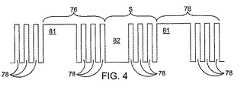
リソグラフィにおいては、クリアフィールドとは一般にオープンスペース(例えばエッチングされている)によって囲まれた一連の周期的構造をいい、ダークフィールドとは一般にクローズドスペース(例えばエッチングされていない)によって囲まれた一連の周期的構造をいう。クリアフィールドは一般に明るく見え、ダークフィールドは一般に暗く見える。この特定の実施形態においては、クリアフィールドは、図3のバーのような細かくセグメント化された要素のグループ間の空き地であり、ダークフィールドは、図3のバーのような細かくセグメント化された要素のグループ間の閉じた空間である。クリアフィールドおよびダークフィールドは、広くなったり細くなったりしたバーによって生じる見かけのズレが打ち消しあったりバランスを取ってなくなるように、線群の形成を変えるよう構成されえると一般に考えられる。ある実現例においては、バランスはそれぞれの周期的構造内で取られる。例えばワーキング・ゾーンのそれぞれは、クリアフィールドおよびダークフィールドの両方を備えた細かいセグメントを含む。例えば粗くセグメント化された線のいくつかはクリアフィールドを持ち、いくつかはダークフィールドを持つ。別の実現例においては、異なるワーキング・ゾーンの2つの周期的構造間でバランスが取られる。例えば、少なくとも第1ワーキング・ゾーンはクリアフィールドを備えた細かいセグメントを持つ周期的構造を含み、少なくとも第2ワーキング・ゾーンはダークフィールドを備えた細かいセグメントを持つ周期的構造を含む。たいていの場合、第1および第2ワーキング・ゾーンは、同じレイヤ上にある対向したワーキング・ゾーンである。これらの実現例は、図4および5を参照して以下に詳細に説明される。
【0068】
図4は本発明のある実施形態による図2に示される周期的構造74のいずれかの部分側面立面図である。例として、図4は一般に上述の第1実現例に対応する。示されるように、粗くセグメント化された線76は、複数の細かくセグメント化されたバー78と、少なくとも一つのダークフィールド81とによって形成される。粗くセグメント化された線群76は、複数の細かくセグメント化されたバー78と、少なくとも一つのクリアフィールド82とを含むセパレーションSによって分割される。細かくセグメント化された線群、ダークフィールドおよびクリアフィールドの幾何学的配置は大きく変えることができる。これらの要素の幾何学的配置は一般に、照明の部分可干渉性と、ステッパレンズの光学系のコマ収差とに依存する。線群とスペース群とが部分的にセグメント化されるデュアルトーン構造は、それらのどちらか一つしか備えない構造よりも、装置構造によってもたらされるパターン配置誤差をより改善する傾向にある。
【0069】
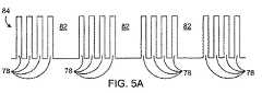
図5AおよびBは本発明のある実施形態による2つの別個の周期的構造群84の部分側面立面図である。たいていの場合、周期的構造群84および85は、対向するワーキング・ゾーンからなり、同じレイヤ内に位置する周期的構造を表す。例えば周期的構造84は、周期的構造74Aに対応しえ、一方、周期的構造85は周期的構造72Dに対応しえる。しかしこれは限定事項ではないことに注意されたい。
【0070】
図5Aを参照して、第1周期的構造84は、粗くセグメント化された線群76を含み、これら線群は複数の細かくセグメント化されたバー78によって形成され、これら線群はクリアフィールド82によって分離されている。図5Bを参照して、第2周期的構造85は、粗くセグメント化された線群76を含み、これら線群は複数の細かくセグメント化されたバー78によって形成され、これら線群はダークフィールド81によって分離されている。細かくセグメント化された線、ダークフィールドおよびクリアフィールドの幾何学的配置は大きく変えることができる。この特定の実施形態においては、ダークフィールドのサイズ・形状(反対ではあるが)および位置は、クリアフィールドのサイズ・形状(反対ではあるが)および位置に一般に対応する。
【0071】
上記説明からわかるように、X字構成の効果は多い。例えば、X字構成は、マークの周縁を中心からエッジまで満たす標準的なボックスインボックスターゲットよりもより多くの情報を提供する。またその長さとともにエッジ(例えば粗くセグメント化された線)の数を増すことによって、より多くの情報を提供する。エッジの数とその長さを増すことによってより多くの情報を提供すること以外に、X字構成は、もともと備わっている追加の対称性のおかげで、通常のボックスインボックスターゲットよりもさらなる効果を提供する。すなわち、通常のボックスインボックス構造においては、内側および外側のレイヤが存在する。これらが入れ替わると、内側および外側マークの異なる情報分布のため、および視野中心に近い領域および視野中心から遠い領域における計測ツールの異なる光学的ふるまいのため、異なるパターンになり、よって異なる重ね合わせ結果を生む。この点から、X字ターゲット構造は基本的にレイヤ入れ替え(鏡像変換まで)に関して不変である。さらにX字構成は、非対称コマパターンを克服するのに役立つ、つまりコマ収差が打ち消し合う180度回転対称性を示す。
【0072】
図6は、本発明の他の実施形態による重ね合わせマーク90の上から見た平面図である。例として、重ね合わせマーク90は図2に示す重ね合わせマークに概ね対応する。重ね合わせマーク90は、2つのウェーハレイヤ(一つはクロスハッチングされており、もう一つはされていない)間のレジストレーション誤差を決定するための4つのワーキング・ゾーン92A〜Dを含む。ワーキング・ゾーンのそれぞれは、複数の粗くセグメント化された線96によって構成される周期的構造94を含む。図2のX字ターゲットと似て、第1および第4ゾーン92AおよびDに位置する周期的構造94AおよびDは、ウェーハの第1レイヤ内に配置され、一方、第2および第3ゾーン92BおよびCに位置する周期的構造94BおよびCは、ウェーハの第2レイヤ内に配置される。さらに同じレイヤ上の周期的構造は、例えば構造94AおよびDのように、対角線上に対向して位置し、それによりX字構成で重ね合わせマークを形成する。
【0073】
この特定の実施形態においては、粗くセグメント化された線は水平に位置し、それによりこれらはY方向の重ね合わせを測定するように構成される。しかし、これは限定事項ではなく、ターゲットは回転されてX方向の重ね合わせを測定してもよいことに注意されたい。またこの実施形態においては、粗くセグメント化された線が伸長され、形状が長方形の中身のつまった構造であるが、これは限定事項ではなく、粗くセグメント化された線は、図4において説明された細かくセグメント化された要素にしたがって作られる複数の細かくセグメント化された要素によって形成されてもよいことに注意されたい。
【0074】
図2のマークと対照的に、ワーキング・ゾーン92のそれぞれは、特に図6の周期的構造94のそれぞれは、マーク90の中心に追加構造96を収めるために「L字形状の」輪郭または形状を持つ。図示された実施形態において追加構造96は、本願の背景において説明された標準的なボックスインボックス構造を表す。よって「X字」で構成されたマーク90は、標準的なボックスインボックス計測ツールおよびアルゴリズムによって捕捉され測定されえる、つまり既存の装置およびソフトウェアが使用可能である。
【0075】
図7は、本発明の他の実施形態による重ね合わせマーク100の上から見た平面図である。例として重ね合わせマーク100は図2に示された重ね合わせマークと概ね対応する。重ね合わせマーク100は、2つのウェーハレイヤ(一つはクロスハッチングされており、もう一つはされていない)間のレジストレーション誤差を決定するための4つのワーキング・ゾーン102A〜Dを含む。ワーキング・ゾーンのそれぞれは、複数の粗くセグメント化された線106によって構成される周期的構造104を含む。図2のX字ターゲットと似て、第1および第4ゾーン102AおよびDに位置する周期的構造104AおよびDは、ウェーハの第1レイヤ内に配置され、一方、第2および第3ゾーン102BおよびCに位置する周期的構造104BおよびCは、ウェーハの第2レイヤ内に配置される。さらに同じレイヤ上の周期的構造は、例えば構造104AおよびDのように、対角線上に対向して位置し、それによりX字構成で重ね合わせマークを形成する。
【0076】
この特定の実施形態においては、粗くセグメント化された線106は水平に位置し、それによりこれらはY方向の重ね合わせを測定するように構成される。しかし、これは限定事項ではなく、マーク100は回転されてX方向の重ね合わせを測定してもよいことに注意されたい。またこの実施形態においては、粗くセグメント化された線が伸長され、形状が長方形の中身のつまった構造である。これは限定事項ではなく、粗くセグメント化された線は、図4において説明された細かくセグメント化された要素にしたがって作られる複数の細かくセグメント化された要素によって形成されてもよいことに注意されたい。
【0077】
図2のマークと対照的に、ワーキング・ゾーン102のそれぞれは、特に図7の周期的構造104のそれぞれは、マーク100の中心に追加構造108を収めるために「長方形の」輪郭または形状を持つ。図示された実施形態において追加構造108は、本願の背景において説明された標準的なボックスインボックス構造を表す。よって「X字」で構成されたマーク100は、標準的なボックスインボックス計測ツールおよびアルゴリズムによって捕捉され画像化されえる。しかしこれは限定事項ではなく、追加構造は他の構造、例えば、光学的パターン認識ツールおよびアルゴリズムによって認識および捕捉されえるパターン認識構造を表しえる。いずれの構成も、既存の装置およびソフトウェアに変更の必要がないという効果を有する。
【0078】
図8は、本発明の他の実施形態による重ね合わせマーク110の上から見た平面図である。例として重ね合わせマーク110は図2に示されたマークと対応しえる。しかし図2のマークとは異なり、重ね合わせマーク110は重ね合わせを2つの異なる向きについて測定するように構成されることに注意されたい。よってマーク110は重ね合わせが測定されるのに必要な、それぞれの向きのための一つのマークの必要性をなくす。重ね合わせマーク110は、ウェーハのテストされるレイヤが完全にアライメントしているときに結果として生じる構成において示されている。
【0079】
重ね合わせマーク110は、2つの異なる向きにおける2つのウェーハレイヤ間のレジストレーション誤差を決定するための複数のワーキング・ゾーン112を含む。示された実施形態において重ね合わせマーク110は、4つの正方形状のワーキング・ゾーン112を含み、これらは重ね合わせマーク110を画像化するのに用いられる計測ツールの視野(不図示)を実質的に埋めるように構成される。ワーキング・ゾーン112は、ウェーハの異なるレイヤ間のアライメントを計算するの用いられるマークの実際の領域を表す。前述のように、ワーキング・ゾーン112は空間的に互いに分離され、その結果、それらは第2レイヤの隣接するワーキング・ゾーンの部分と重ならないようになっている。
【0080】
この実施形態においては、ワーキング・ゾーンは、例えばXおよびY方向の2つの向きにおける重ね合わせ情報を提供するように構成される。4つのワーキング・ゾーン112A〜Dのうち、2つのワーキング・ゾーン112AおよびDは第1レイヤに配置され、2つのワーキング・ゾーン112BおよびCは第2レイヤに配置される(第1レイヤは中が塗りつぶされており、第2レイヤは中が塗りつぶされていない)。同じ第1レイヤ上に配置されるワーキング・ゾーン112AおよびDは第1垂直角で互いに対向し、同じ第2レイヤ上に配置されるワーキング・ゾーン112BおよびCは第2垂直角で互いに対向する(例えば対角線上に)。これらの交わって配置された構造は「X字」形パターンを形成する。
【0081】
ワーキング・ゾーン112のそれぞれは、例えば周期的構造114A〜Dのような個別の周期的構造114を含む。示されるように、周期的構造114のそれぞれは実質的にその対応するワーキング・ゾーン112の周縁を埋める。理解されるように、周期的構造114のそれぞれはその対応するワーキング・ゾーン112のレイヤ内に形成される。周期的構造114は、ロウとカラムとに分割されて間隔が空けられて配置された粗くセグメント化された要素116を含む。粗くセグメント化された要素116のそれぞれは、こんどは、細かくセグメント化された要素118によって形成される。細かくセグメント化された要素118はまた、ロウとカラムとに分割されて間隔が空けられて配置される。個別の粗くセグメント化された要素116および細かくセグメント化された要素118は、さまざまなサイズ、形状および分布で構成されえる。示された実施形態においては、粗くセグメント化された要素116および細かくセグメント化された要素118の両方は、正方形の形をして、隣接する要素から等しく距離を置かれている。理解されるように、重ね合わせマーク110は、同じ繰り返し構造パターンを直交する向きに持つので、互いに垂直である2つの異なる向きにおけるミスレジストレーション値を測定するのに使用可能である。
【0082】
図9は、本発明の他の実施形態による重ね合わせマーク130の上から見た平面図である。例として重ね合わせマーク130は図2のマークと対応する。しかし図2のマークとは異なり、重ね合わせマーク110は重ね合わせを2つの異なる向きについて測定するように構成されることに注意されたい。よってマーク130は重ね合わせが測定されるのに必要な、それぞれの向きのための一つのマークの必要性をなくす。重ね合わせマーク130は、ウェーハのテストされるレイヤが完全にアライメントしているときに結果として生じる構成において示されている。重ね合わせマーク130は一般に、ウェーハの2つ以上の連続するレイヤ間の、またはウェーハの単一のレイヤ上に別個に生成された2つ以上のパターン間の相対的なズレを決定するのに提供される。議論を簡単にするために、重ね合わせマーク130は、基板の異なるレイヤ間の重ね合わせを測定する場合において説明される。しかしこの図の重ね合わせマークはまた、基板の単一のレイヤ上の2以上の個別に生成されたパターンを測定するのに用いられてもよいことに注意されたい。
【0083】
重ね合わせマーク130は、2つの異なる向きにおける2つのウェーハレイヤ間のレジストレーション誤差を決定するための複数のワーキング・ゾーン132を含む。示された実施形態において重ね合わせマーク130は、8つの長方形状のワーキング・ゾーン132を含み、これらはその周縁71を実質的に埋めるように構成される。ワーキング・ゾーン132は、ウェーハの異なるレイヤ間のアライメントを計算するの用いられるマークの実際の領域を表す。前述のように、ワーキング・ゾーン132は空間的に互いに分離され、その結果、それらは第2レイヤの隣接するワーキング・ゾーンの部分と重ならないようになっている。この特定の構成においては、ワーキング・ゾーンのいくつかは除外ゾーンを介して分離されており、一方、他のワーキング・ゾーンは隣接ワーキング・ゾーンの隣に位置する。例えばワーキング・ゾーン132Bはワーキング・ゾーン132EおよびFから除外ゾーン133を介して分離されており、一方、ワーキング・ゾーン132EおよびFはそのエッジにおいて互いに隣り合って位置する。
【0084】
議論を進めるために、ワーキング・ゾーン132は、第1ワーキング・グループ134および第2ワーキング・グループ136にグループ分けされる。第1ワーキング・グループ134は、第1方向における重ね合わせ情報を提供するように構成される4つのワーキング・ゾーン132A〜Dを含む。例として、第1方向はY方向でありえる。4つのワーキング・ゾーン132A〜Dのうち、2つのワーキング・ゾーン132AおよびDは第1レイヤに設けられ、2つのワーキング・ゾーン132BおよびCは第2レイヤに設けられる(第1レイヤはクロスハッチングで表され、第2レイヤはクロスハッチングなしで表される)。理解されるように、このマーク構成について、重ね合わせ誤差がゼロの場合(図示のとおり)、ワーキング・ゾーン132AおよびD、およびワーキング・ゾーン132BおよびCの対称の中心135は正確に一致する。第2ワーキング・グループ136は、第1方向と垂直な第2方向における重ね合わせ情報を提供するように構成される4つのワーキング・ゾーン132E〜Hを含む。例として、第2方向はX方向でありえる。4つのワーキング・ゾーン132E〜Hのうち、2つのワーキング・ゾーン132EおよびHは第1レイヤに設けられ、2つのワーキング・ゾーン132FおよびGは第2レイヤに設けられる(第1レイヤはクロスハッチングで表され、第2レイヤはクロスハッチングなしで表される)。上述のように、このマーク構成について、重ね合わせ誤差がゼロの場合(図示のとおり)、ワーキング・ゾーン132EおよびH、およびワーキング・ゾーン132FおよびGの対称の中心137は正確に一致する。
【0085】
理解されるように、グループ134および136のそれぞれは「X字」構成のマークを表す(オフセットはあるが)。例えばワーキング・グループ134は、同じ第1レイヤ上にあり、互いに対角線上に対向する位置にあるワーキング・ゾーン132AおよびDと、同じ第2レイヤ上にあり、互いに対角線上に対向する位置にあるワーキング・ゾーン132BおよびCを含む。さらにワーキング・ゾーン132AおよびDは、ワーキング・ゾーン132BおよびCに対して角度がつけられている。さらに、ワーキング・ゾーン132Aは空間的にワーキング・ゾーン132Dからオフセットが設けられており、ワーキング・ゾーン132Bは空間的にワーキング・ゾーン132Dからオフセットが設けられている。
【0086】
さらにワーキング・ゾーン136は、同じ第1レイヤ上にあり、互いに対角線上に対向する位置にあるワーキング・ゾーン132EおよびHと、同じ第2レイヤ上にあり、互いに対角線上に対向する位置にあるワーキング・ゾーン132FおよびGを含む。さらにワーキング・ゾーン132EおよびHは、ワーキング・ゾーン132FおよびGに対して角度がつけられている。さらに、ワーキング・ゾーン132Eは空間的にワーキング・ゾーン132Hからオフセットが設けられており、ワーキング・ゾーン132Fは空間的にワーキング・ゾーン132Gからオフセットが設けられている。本質的に、この特定のマークは、互いに対角線上にある2つの「X字」構成のマーク群、つまりワーキング・グループ194およびワーキング・グループ196を作る。
【0087】
さらに詳述するなら、あるレイヤ上のワーキング・ゾーンは、一般に他のレイヤ上のワーキング・ゾーンに対して並置される。例えば第1ワーキング・グループにおいて、ワーキング・ゾーン132Aはワーキング・ゾーン132Bに対して並置され、ワーキング・ゾーン132Cはワーキング・ゾーン132Dに対して並置される。同様に、第2ワーキング・グループにおいて、ワーキング・ゾーン132Eはワーキング・ゾーン132Hに対して並置され、ワーキング・ゾーン132Fはワーキング・ゾーン132Gに対して並置される。2つの並置されたペアのうち、第2レイヤ上のワーキング・ゾーンは典型的には第1レイヤ上のワーキング・ゾーンよりもFOVの中心により近く位置する。例えば、ワーキング・ゾーン132BおよびCおよびワーキング・ゾーン132FおよびGはそれぞれ、それらの並置されたワーキング・ゾーン132AおよびDおよびワーキング・ゾーン132EおよびHよりもFOV144の中心142により近く位置する。さらに、ワーキング・グループ群のそれぞれの中で、並置されたペアはグループ内の他の並置されたペアに対して対向する関係に(例えば対角線上に)位置する。例えば、並置されたペア132AおよびBは、並置されたペア132CおよびDに対向して位置し、並置されたペア132EおよびFは、並置されたペア132GおよびHに対向して位置する。
【0088】
理解されるように、この特定のマークにおいて、ワーキング・ゾーンの構成は回転対称(マークの中心を軸に±90、180、270、360度)である。これは典型的には、計測ツールの視野にわたる半径方向および軸方向のバラツキ、例えば、不均一光学収差およびツールに起因するズレ(TIS)を起こす照明によって引き起こされる半径方向および軸方向のバラツキの影響を低減するためになされる。半径方向のバラツキとは一般に、マークの中心からマークの外周領域へと広がるバラツキをいう。軸方向のバラツキとは一般に、マークの軸に沿った向きにおいて発生するバラツキをいい、例えばX方向においてはマークの左から右の部分へであり、Y方向においてはマークの下から上の部分へである。
【0089】
ワーキング・ゾーン132A〜Hのそれぞれは、複数の粗くセグメント化された線群140によって構成される周期的構造138を含む。粗くセグメント化された線群の線幅Dおよび間隔sは大きく変更しえる。示されるように、周期的構造138のそれぞれは実質的にその対応するワーキング・ゾーン132の周縁を埋める。理解されるように、周期的構造138はまたその対応するワーキング・ゾーン132のレイヤ上に配置される。
【0090】
議論を簡単にするために、周期的構造138は、第1ワーキング・グループ134と関連する第1周期的構造138Aと、第2ワーキング・グループと関連する第2周期的構造138Bとに分類されえる。示されるように、第1周期的構造138Aはすべて同じ向きに方向づけられている。つまり粗くセグメント化された線群140は平行で互いに水平に位置する。第2周期的構造138Bもすべて同じ向きに方向づけられている(第1周期的構造とは異なるが)。つまり粗くセグメント化された線群140は平行で互いに垂直に位置する。よって第1ワーキング・グループ134内の周期的構造138Aは、第2ワーキング・グループ136内の周期的構造138Bに対して直交する。
【0091】
ある実施形態においては、並置される周期的構造の粗くセグメント化された線群は互いにアラインされている。つまりもし異なるレイヤを無視するなら、連続的なグレーティングをなすように見える。例えばワーキング・ゾーン132Aの粗くセグメント化された線は、ワーキング・ゾーン132Bの粗くセグメント化された線とアラインされ、ワーキング・ゾーン132Cの粗くセグメント化された線は、ワーキング・ゾーン132Dの粗くセグメント化された線とアラインされる。さらにワーキング・ゾーン132Eの粗くセグメント化された線は、ワーキング・ゾーン132Fの粗くセグメント化された線とアラインされ、ワーキング・ゾーン132Gの粗くセグメント化された線は、ワーキング・ゾーン132Hの粗くセグメント化された線とアラインされる。
【0092】
図10は、本発明の他の実施形態による重ね合わせマーク150の上から見た平面図である。この特定の実施形態においては、粗くセグメント化された線140は複数の細かくセグメント化された要素152によって形成される。細かくセグメント化された要素152は図2で説明された細かくセグメント化された要素178に概ね対応する。
【0093】
図11は、本発明の他の実施形態による重ね合わせマーク170の上から見た平面図である。例として、重ね合わせマーク170は図6および9に示された重ね合わせマークに概ね対応する。重ね合わせマーク130と同様に、重ね合わせマーク170は、2つの異なる向きにおける2つのウェーハレイヤ間のレジストレーション誤差を決定するための8つのワーキング・ゾーン172A〜Hを含む(一方のレイヤはクロスハッチングで表され、もう一方はなしで表される)。ワーキング・ゾーンのそれぞれは、複数の粗くセグメント化された線176によって構成された周期的構造174を含む。重ね合わせマーク90と同様に、ワーキング・ゾーン172のそれぞれは、マーク170の中心に追加構造178を収めるように構成される。図示された実施形態においては、ワーキング・ゾーン172A〜Hは、マークの外側領域周辺に配置され、一方、追加構造178はマークの中心に配置される。追加構造178は、本願の背景で説明された標準的なボックスインボックス構造を表す。よってマーク170は、標準的なボックスインボックス計測ツールおよびアルゴリズムによって捕捉され測定されえる、つまり既存の装置およびソフトウェアが使用可能である。
【0094】
図12は、本発明の他の実施形態による重ね合わせマーク190の上から見た平面図である。例として、重ね合わせマーク190は図9のマークに対応する。図9のマークのように、図12の重ね合わせマーク170は、2つの別々の向きにおける重ね合わせを測定するように構成される。よって、マーク190は重ね合わせが測定されるのに必要な、それぞれの向きのための一つのマークの必要性をなくす。図9のマークとは対照的に、マーク190は三角形の形をしたワーキング・ゾーンを含む。重ね合わせマーク190は、テストされているウェーハのレイヤが完全なアライメントにあるときに生じる構成で表されている。
【0095】
重ね合わせマーク190は、2つの異なる向きにおける2つのウェーハレイヤ間のレジストレーション誤差を決定するための複数のワーキング・ゾーン192を含む。示された実施形態において、重ね合わせマーク140は、その周縁を実質的に埋めるように構成された8つの三角形の形をしたワーキング・ゾーン192を含む。ワーキング・ゾーン192は、ウェーハの異なるレイヤ間のアライメントを計算するの用いられるマークの実際の領域を表す。前述のように、ワーキング・ゾーン192は空間的に互いに分離され、その結果、それらは隣接するワーキング・ゾーンの部分と重ならないようになっている。この特定の実施形態においては、ワーキング・ゾーン192のすべてが除外ゾーン193を介して分離されている。
【0096】
議論を進めるために、ワーキング・ゾーン192は、第1ワーキング・グループ194および第2ワーキング・グループ196にグループ分けされる。第1ワーキング・グループ194は、第1方向における重ね合わせ情報を提供するように構成される4つのワーキング・ゾーン192A〜Dを含む。例として、第1方向はY方向でありえる。4つのワーキング・ゾーン192A〜Dのうち、2つのワーキング・ゾーン192AおよびDは第1レイヤに設けられ、2つのワーキング・ゾーン192BおよびCは第2レイヤに設けられる(第1レイヤは実線で表され、第2レイヤは点線で表される)。理解されるように、このマーク構成について、重ね合わせ誤差がゼロの場合(図示のとおり)、ワーキング・ゾーン192AおよびD、およびワーキング・ゾーン192BおよびCの対称の中心195は正確に一致する。第2ワーキング・グループ196は、第1方向と垂直な第2方向における重ね合わせ情報を提供するように構成される4つのワーキング・ゾーン192E〜Hを含む。例として、第2方向はX方向でありえる。4つのワーキング・ゾーン192E〜Hのうち、2つのワーキング・ゾーン192EおよびHは第1レイヤに設けられ、2つのワーキング・ゾーン192FおよびGは第2レイヤに設けられる(第1レイヤは実線で表され、第2レイヤは点線で表される)。上述と同様に、このマーク構成について、重ね合わせ誤差がゼロの場合(図示のとおり)、ワーキング・ゾーン192EおよびH、およびワーキング・ゾーン192FおよびGの対称の中心197は正確に一致する。さらにワーキング・ゾーン192の全てはマークの中心に対して等しく位置する。
【0097】
理解されるように、グループ194および196のそれぞれは「X字」構成のマークを表す。例えばワーキング・グループ194は、同じ第1レイヤ上にあり、互いに対角線上に対向する位置にあるワーキング・ゾーン192AおよびDと、同じ第2レイヤ上にあり、互いに対角線上に対向する位置にあるワーキング・ゾーン192BおよびCを含む。さらにワーキング・ゾーン192AおよびDは、ワーキング・ゾーン192BおよびCに対して角度がつけられている。さらに、ワーキング・ゾーン192Aは空間的にワーキング・ゾーン192Dからオフセットが設けられており、ワーキング・ゾーン192Bは空間的にワーキング・ゾーン192Dからオフセットが設けられている。
【0098】
さらにワーキング・グループ136は、同じ第1レイヤ上にあり、互いに対角線上に対向する位置にあるワーキング・ゾーン192EおよびHと、同じ第2レイヤ上にあり、互いに対角線上に対向する位置にあるワーキング・ゾーン192FおよびGを含む。さらにワーキング・ゾーン192EおよびHは、ワーキング・ゾーン192FおよびGに対して角度がつけられている。さらに、ワーキング・ゾーン192Eは空間的にワーキング・ゾーン192Hからオフセットが設けられており、ワーキング・ゾーン192Fは空間的にワーキング・ゾーン192Gからオフセットが設けられている。本質的に、この特定のマークは、互いに対角線上にある2つの「X字」構成のマーク群、つまりワーキング・グループ194およびワーキング・グループ196を作る。
【0099】
さらに詳述するなら、あるレイヤ上のワーキング・ゾーンは、一般に他のレイヤ上のワーキング・ゾーンに対して並置される。例えば第1ワーキング・グループにおいて、ワーキング・ゾーン192Aはワーキング・ゾーン192Bに対して並置され、ワーキング・ゾーン192Cはワーキング・ゾーン192Dに対して並置される。同様に、第2ワーキング・グループにおいて、ワーキング・ゾーン192Eはワーキング・ゾーン192Hに対して並置され、ワーキング・ゾーン192Fはワーキング・ゾーン192Gに対して並置される。このマーク構成について、重ね合わせがゼロの場合(図示のように)、ワーキング・ゾーン192のすべてがマークの中心に対して等しく位置する。さらに、ワーキング・グループ群のそれぞれの中で、並置されたペアはグループ内の他の並置されたペアに対して対向する関係に(例えば上/下および右/左に)位置する。例えば、並置されたペア192AおよびBは、並置されたペア192CおよびDに対向して位置し、並置されたペア192EおよびFは、並置されたペア192GおよびHに対向して位置する。
【0100】
理解されるように、この特定のマークにおいて、ワーキング・ゾーンの構成は中心または周縁を他のレイヤについてずらせることなく、回転対称(マークの中心を軸に±90、180、270、360度)である。つまりマークは不変である。これは典型的には、計測ツールの視野にわたる半径方向および軸方向のバラツキ、例えば、不均一光学収差およびツールに起因するズレ(TIS)を起こす照明によって引き起こされる半径方向および軸方向のバラツキの影響を低減するためになされる。
【0101】
ワーキング・ゾーン192のそれぞれは、複数の粗くセグメント化された線群200によって構成される周期的構造198を含む。粗くセグメント化された線群の線幅Dおよび間隔sは大きく変更しえる。示されるように、周期的構造198のそれぞれは実質的にその対応するワーキング・ゾーン192の周縁を埋める。理解されるように、周期的構造198はまたその対応するワーキング・ゾーン192のレイヤ上に配置される。
【0102】
議論を簡単にするために、周期的構造198は、第1ワーキング・グループ194と関連する第1周期的構造198Aと、第2ワーキング・グループ196と関連する第2周期的構造198Bとに分類されえる。示されるように、第1周期的構造198Aはすべて同じ向きに方向づけられている。つまり粗くセグメント化された線群190Aは平行で互いに水平に位置する。第2周期的構造198Bもすべて同じ向きに方向づけられている(第1周期的構造とは異なるが)。つまり粗くセグメント化された線群198Bは平行で互いに垂直に位置する。よって第1ワーキング・グループ194内の周期的構造198Aは、第2ワーキング・グループ196内の周期的構造198Bに対して直交する。さらに、FOV内にそれぞれのゾーンを収めるために、粗くセグメント化された線190は、マークの外側領域からマークの内側領域へと移るにつれてその長さを減少させる。図示はされないが、このマークをさらに改善するために、粗くセグメント化された線は、複数の細かくセグメント化された要素によって形成されえる。
【0103】
図13は、本発明の他の実施形態による重ね合わせマーク210の上から見た平面図である。示されるようにマーク210は、図12のマーク190と同じおおまかなレイアウトおよび特徴を持つ。つまり8つの三角形の形をしたワーキング・ゾーンを持つ。しかしマーク210はマークの中心を2つのレイヤのうちの一つの上に形成されたグレーティングパターン212についてずらしている点でマーク190とは異なる。グレーティングパターン212は、コントラストまたは粒度のために、あるレイヤにおけるマークの質が他のレイヤにおけるマークの質よりも低いときに典型的には用いられる。すなわちコントラストが低いときのレイヤ内の情報(例えばエッジ)は増す。あるいは、あるレイヤについてFOVの中心をずらすことはプロセスダメージからそれを保護するかもしれない。グレーティングパターン212は大きく変更しえる。例えばグレーティングパターンはいかなる本数の線群をも、いかなる数の分布およびサイズで含みえる。この特定の実施形態においては、グレーティングパターンは第2レイヤ上に形成され、マークの中心の周りに方向が交互に変わる(例えばXおよびY方向)2つの粗くセグメント化された線214のグループからなる。
【0104】
図14は、本発明の他の実施形態による重ね合わせマーク220の上から見た平面図である。例として、重ね合わせマーク220は図9に示す重ね合わせマークに概ね対応する。図9のマークのように、重ね合わせマーク220は、2つの別々の向きにおける重ね合わせを測定するように構成される。よって、マーク220は重ね合わせが測定されるのに必要な、それぞれの向きのための一つのマークの必要性をなくす。重ね合わせマーク220は、テストされているウェーハのレイヤが完全なアライメントにあるときに生じる構成で表されている。
【0105】
重ね合わせマーク220は、2つの異なる向きにおける2つのウェーハレイヤ間のレジストレーション誤差を決定するための複数のワーキング・ゾーン222を含む。示された実施形態において、重ね合わせマーク222は、その周縁を実質的に埋めるように構成された16個の正方形の形をしたワーキング・ゾーン222を含む。ワーキング・ゾーン222のそれぞれは粗くセグメント化された線の周期的構造を含む。図示はされないが、ある実施形態では粗くセグメント化された線は複数の細かくセグメント化された要素によって、例えばここで説明されたり図示されたりしたいかなる構成(図3〜5)によって形成されてもよい。
【0106】
16個のワーキング・ゾーンのうち、8個のワーキング・ゾーン222AはX方向を向き、8個のワーキング・ゾーン222BはY方向を向いている(そこに配置される周期的構造によって示されるように)。8個のワーキング・ゾーン222のうち、与えられたいかなる向き(AまたはB)においても、4つのワーキング・ゾーン222’は第1レイヤ上に印刷され(クロスハッチングで表される)、一方、4つのワーキング・ゾーン222”は第2レイヤ上に印刷される(クロスハッチングなしで表される)。ワーキング・ゾーンの向きはさまざまな方法で説明されえる。例えばワーキング・ゾーン222は、正方形の形をしたマーク220の4つの角を形成する4つのグループ224A〜Dに分布されえる。これらのグループ224A〜Dのそれぞれは、異なるレイヤ上に異なる方向に形成されるワーキング・ゾーンによって等しく代表される。すなわち、それぞれのグループは、例えばワーキング・ゾーン222A’、222A”、222B’および222B”の、4つの異なるワーキング・ゾーンを含む。
【0107】
ワーキング・ゾーン222は4つのグループ224E〜Hに分布されてもよく、これらのそれぞれは「X字」構成のマーク(オフセットされてはいるが)を表す。この場合、「X字」構成のマークは3x3のワーキング・ゾーングループの角によって形成される。4つのグループのうち、2つのグループはX方向における重ね合わせを決定し、2つのグループはY方向における重ね合わせを決定する。例えば、対角線上に対向し、空間的にオフセットされたワーキング・ゾーン222B’および222B”を含むワーキング・グループ224EおよびFは、Y方向における重ね合わせを決定する。さらに対角線上に対向し、空間的にオフセットされたワーキング・ゾーン222A’および222A”を含むワーキング・グループ224GおよびHは、X方向における重ね合わせを決定する。
【0108】
図15は、本発明の他の実施形態による重ね合わせマーク240の上から見た平面図である。例として、重ね合わせマーク240は図14に示す重ね合わせマークに概ね対応する。図13の重ね合わせマークのように、重ね合わせマーク240は、2つの別々の向きにおける重ね合わせを測定するように構成される。よって、マーク240は重ね合わせが測定されるのに必要な、それぞれの向きのための一つのマークの必要性をなくす。重ね合わせマーク240は、テストされているウェーハのレイヤが完全なアライメントにあるときに生じる構成で表されている。
【0109】
重ね合わせマーク240は、2つの異なる向きにおける2つのウェーハレイヤ間のレジストレーション誤差を決定するための複数のワーキング・ゾーン242を含む。示された実施形態において、重ね合わせマーク240は、その周縁を実質的に埋めるように構成された16個の正方形の形をしたワーキング・ゾーン242を含む。ワーキング・ゾーン242のそれぞれは粗くセグメント化された線の周期的構造を含む。図示はされないが、ある実施形態では粗くセグメント化された線は複数の細かくセグメント化された要素によって形成されてもよい。
【0110】
16個のワーキング・ゾーンのうち、8個のワーキング・ゾーン242AはX方向を向き、8個のワーキング・ゾーン242BはY方向を向いている(そこに配置される周期的構造によって示されるように)。8個のワーキング・ゾーン242のうち、与えられたいかなる向き(AまたはB)においても、4つのワーキング・ゾーン242’は第1レイヤ上に印刷され(クロスハッチングで表される)、一方、4つのワーキング・ゾーン242”は第2レイヤ上に印刷される(クロスハッチングなしで表される)。ワーキング・ゾーンの向きはさまざまな方法で説明されえる。例えばワーキング・ゾーン242は、正方形の形をしたマーク240の4つの角を形成する4つのグループ244A〜Dに分布されえる。垂直な角度で対向するグループは同じであり、つまり、そこでのワーキング・ゾーンは同じように向いている。それぞれのグループ244A〜Dにおける4つのワーキング・ゾーンのうち、それらの2つは同じレイヤおよび向きを表し、それらの2つは異なるレイヤおよび向きを表す。垂直な角度で互いに対向するこれらのグループのワーキング・ゾーンは同一であり、すなわち、それらは同じレイヤおよび向きを表す。例えば、グループ244AおよびDは、対向するワーキング・ゾーン242A’および対向するワーキング・ゾーン242B”を含み、グループ244BおよびCは、対向するワーキング・ゾーン242B’および対向するワーキング・ゾーン242A”を含む。
【0111】
ワーキング・ゾーン242は4つのグループ244E〜Hに分布されてもよく、これらのそれぞれは「X字」構成のマーク(オフセットされてはいるが)を表す。この場合、「X字」構成のマークは3x3のワーキング・ゾーングループの角によって形成される。4つのグループのうち、2つのグループはX方向における重ね合わせを決定し、2つのグループはY方向における重ね合わせを決定する。例えば、対向するワーキング・ゾーン242B’および242B”を含むワーキング・グループ244EおよびFはY方向における重ね合わせを決定する。さらに、対向するワーキング・ゾーン242A’および242A”を含むワーキング・グループ244GおよびHはX方向における重ね合わせを決定する。
【0112】
図16は、本発明の他の実施形態による重ね合わせマーク250の上から見た平面図である。例として、重ね合わせマーク250は図13に示す重ね合わせマークに概ね対応する。図14の重ね合わせマークのように、重ね合わせマーク250は、2つの別々の向きにおける重ね合わせを測定するように構成される。よって、マーク250は重ね合わせが測定されるのに必要な、それぞれの向きのための一つのマークの必要性をなくす。重ね合わせマーク250は、テストされているウェーハのレイヤが完全なアライメントにあるときに生じる構成で表されている。
【0113】
重ね合わせマーク250は、2つの異なる向きにおける2つのウェーハレイヤ間のレジストレーション誤差を決定するための複数のワーキング・ゾーン252を含む。示された実施形態において、重ね合わせマーク250は、その周縁を実質的に埋めるように構成された16個の正方形の形をしたワーキング・ゾーン252を含む。ワーキング・ゾーン252のそれぞれは粗くセグメント化された線の周期的構造を含む。図示はされないが、ある実施形態では粗くセグメント化された線は複数の細かくセグメント化された要素によって形成されてもよい。
【0114】
16個のワーキング・ゾーンのうち、8個のワーキング・ゾーン252AはX方向を向き、8個のワーキング・ゾーン252BはY方向を向いている(そこに配置される周期的構造によって示されるように)。8個のワーキング・ゾーン252のうち、与えられたいかなる向き(AまたはB)においても、4つのワーキング・ゾーン252’は第1レイヤ上に印刷され(クロスハッチングで表される)、一方、4つのワーキング・ゾーン252”は第2レイヤ上に印刷される(クロスハッチングなしで表される)。示されるように、ワーキング・ゾーン252は4つのグループ254E〜Hに分布されてもよく、これらのそれぞれは「X字」構成のマーク(オフセットされてはいるが)を表す。この場合、「X字」構成のマークは3x3のワーキング・ゾーングループの角によって形成される。4つのグループのうち、2つのグループはX方向における重ね合わせを決定し、2つのグループはY方向における重ね合わせを決定する。例えば、対向するワーキング・ゾーン252B’および252B”を含むワーキング・グループ254EおよびFはY方向における重ね合わせを決定する。さらに、対向するワーキング・ゾーン252A’および252A”を含むワーキング・グループ254GおよびHはX方向における重ね合わせを決定する。
【0115】
図17は、本発明の他の実施形態による重ね合わせマーク270の上から見た平面図である。例として、重ね合わせマーク270は図13に示す重ね合わせマークに概ね対応する。図14の重ね合わせマークのように、重ね合わせマーク270は、2つの別々の向きにおける重ね合わせを測定するように構成される。よって、マーク270は重ね合わせが測定されるのに必要な、それぞれの向きのための一つのマークの必要性をなくす。重ね合わせマーク270は、テストされているウェーハのレイヤが完全なアライメントにあるときに生じる構成で表されている。
【0116】
重ね合わせマーク270は、2つの異なる向きにおける2つのウェーハレイヤ間のレジストレーション誤差を決定するための複数のワーキング・ゾーン272を含む。示された実施形態において、重ね合わせマーク270は、その周縁を実質的に埋めるように構成された16個の正方形の形をしたワーキング・ゾーン272を含む。ワーキング・ゾーン272のそれぞれは粗くセグメント化された線の周期的構造を含む。図示はされないが、ある実施形態では粗くセグメント化された線は複数の細かくセグメント化された要素によって形成されてもよい。
【0117】
16個のワーキング・ゾーンのうち、8個のワーキング・ゾーン272AはX方向を向き、8個のワーキング・ゾーン272BはY方向を向いている(そこに配置される周期的構造によって示されるように)。8個のワーキング・ゾーン272のうち、与えられたいかなる向き(AまたはB)においても、4つのワーキング・ゾーン272’は第1レイヤ上に印刷され(クロスハッチングで表される)、一方、4つのワーキング・ゾーン272”は第2レイヤ上に印刷される(クロスハッチングなしで表される)。さらに8個のワーキング・ゾーン272のうち、与えられたいかなる向き(AまたはB)においても、4つのワーキング・ゾーン272は、第1周期を持つ周期的構造Mを有し(細い線で表される)、一方、4つのワーキング・ゾーン272は、第1周期とは異なる第2周期を持つ周期的構造Nを有する(太い線で表される)。
【0118】
ワーキング・ゾーンの向きはさまざまな方法で説明されえる。例えばワーキング・ゾーン272は、正方形の形をしたマーク270の4つの角を形成する4つのグループ274A〜Dに分布されえる。垂直な角度で対向するグループは同じであり、つまり、そこでのワーキング・ゾーンは同じように向いている。これらのグループ274A〜Dのそれぞれは4つの異なるワーキング・ゾーンを含み、これらはレイヤ、向き、または周期の異なる組み合わせ表しえる。これらのグループの中で垂直な角度で互いに対向するワーキング・ゾーンは、同じ向きではあるが、異なるレイヤおよび周期を表す。例えば、グループ272AおよびDは、ワーキング・ゾーン272B−N’に対向するワーキング・ゾーン272A−M’、およびワーキング・ゾーン272B−N”に対向するワーキング・ゾーン272A−M”を含み、グループ272BおよびCは、ワーキング・ゾーン272A−N’に対向するワーキング・ゾーン272B−M’、およびワーキング・ゾーン272A−N”に対向するワーキング・ゾーン272B−M”を含む。
【0119】
ワーキング・ゾーン272は4つのグループ274E〜Hに分布されてもよく、これらのそれぞれは「X字」構成のマーク(オフセットされてはいるが)を表す。この場合、「X字」構成のマークは3x3のワーキング・ゾーングループの角によって形成される。4つのグループのうち、2つのグループはX方向における重ね合わせを決定し、2つのグループはY方向における重ね合わせを決定する。さらに、これらの2つは第1周期を表し、これらの2つは第2周期を表す。例えば、対向するワーキング・ゾーン272B−M’および272B−M”を含むワーキング・グループ274Eは、Y方向における重ね合わせを決定する第1周期を持ち、対向するワーキング・ゾーン272B−N’および272B−N”を含むワーキング・グループ274Fは、Y方向における重ね合わせを決定する第2周期を持つ。さらに、対向するワーキング・ゾーン272A−M’および272A−M”を含むワーキング・グループ274Gは、X方向における重ね合わせを決定する第1周期を持ち、対向するワーキング・ゾーン272A−N’および272A−N”を含むワーキング・グループ274Hは、X方向における重ね合わせを決定する第2周期を持つ。
【0120】
理解されるように、この構成は、2つのグレーティング周期のうちの一つについて改善されたプロセスロバスト性および/または改善されたコントラストを実現し、それにより特定のプロセスについて最適化された周期および/または線幅の選択を可能にする。
【0121】
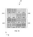
図18は、本発明の他の実施形態による重ね合わせマーク290の上から見た平面図である。例として、重ね合わせマーク290は図13に示す重ね合わせマークに概ね対応する。図14の重ね合わせマークのように、重ね合わせマーク290は、2つの別々の向きにおける重ね合わせを測定するように構成される。よって、マーク290は重ね合わせが測定されるのに必要な、それぞれの向きのための一つのマークの必要性をなくす。図13の重ね合わせマークとは異なり、重ね合わせマーク290はまた3つの連続するウェーハのレイヤ群の間の、または単一のウェーハのレイヤ上の3つの別々に生成されたパターン群の間の相対的なズレを決定するように構成される。議論を簡単にするために、重ね合わせマーク290は基板上の異なるレイヤ群間の重ね合わせを測定する場合について説明される。しかしこの図の重ね合わせマークはまた、基板の単一のレイヤ上の2つ以上の別々に生成されたパターン群を測定するにも用いることができることに注意されたい。重ね合わせマーク290は、テストされているウェーハのレイヤが完全なアライメントにあるときに生じる構成で表されている。
【0122】
重ね合わせマーク290は、2つの異なる向きにおける2つのウェーハレイヤ間のレジストレーション誤差を決定するための複数のワーキング・ゾーン292を含む。示された実施形態において、重ね合わせマーク290は、その周縁7を実質的に埋めるように構成された16個の正方形の形をしたワーキング・ゾーン292を含む。ワーキング・ゾーン292のそれぞれは粗くセグメント化された線の周期的構造を含む。図示はされないが、ある実施形態では粗くセグメント化された線は複数の細かくセグメント化された要素によって形成されてもよい。
【0123】
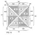
16個のワーキング・ゾーン292のうち、8個のワーキング・ゾーン292AはX方向を向き、8個のワーキング・ゾーン292BはY方向を向いている(そこに配置される周期的構造によって示されるように)。さらに、8個のワーキング・ゾーン292’は第1レイヤ上に印刷され(クロスハッチングで表される)、4つのワーキング・ゾーン292”は第2レイヤ上に印刷され(クロスハッチングなしで表される)、4つのワーキング・ゾーン292”’は第3レイヤ上に印刷される(塗りつぶしで表される)。さらに8個のワーキング・ゾーン272のうち、与えられたいかなる向き(AまたはB)においても、4つのワーキング・ゾーン272は、第1周期を持つ周期的構造Mを有し(細い線で表される)、一方、4つのワーキング・ゾーン272は、第1周期とは異なる第2周期を持つ周期的構造Nを有する(太い線で表される)。この特定の実施形態においては、第1レイヤ(シングルプライムでも表される)は第2レイヤ(ダブルプライムでも表される)の上に配置され、第2レイヤは第3レイヤ(トリプルプライムでも表される)の上に配置される。例として、第1レイヤはレジストレイヤを表し、第2レイヤは第1金属レイヤを表し、第3レイヤは第2金属レイヤを表す。
【0124】
上述の構成は大きく変更できることに注意されたい。例えば8個のワーキング・ゾーンのうち、与えられたいかなる向き(AまたはB)においても、2つは第1レイヤ上に印刷され、一方、グレーティングのそれぞれの追加ペアは3つの以前のレイヤ群のうちのいずれにも印刷されえる。
【0125】
上述の重ね合わせマークの全ては、計測ツールによって生じる不均一性(例えば収差および照明)および/またはプロセスによって生じる不均一性(例えばディッシングおよびエロージョン)を少なくともバランスさせるように構成される。例えばマークのいくつかは重ね合わせ測定に対する半径方向のバラツキの影響を低減させるように構成され、一方、マークの他のものは軸方向のバラツキの影響を低減させるように構成される。
【0126】
図19は、上述のいずれかのマークにおける重ね合わせを画像化を介して測定するのに用いられる重ね合わせ測定システムまたは計測ツール320の簡略化された概略図である。画像化は、多くのユーザの支持と、ユーザがすぐに利用できる要素とを持った非常に発達した技術である。一般に知られるように、画像化は大量の情報を一度に集める効率的な方法である。すなわちマーク内の全ての点が同時に測定されえる。さらに画像化はユーザが実際にウェーハ上で測定されているものを見ることを可能にする。さまざまな要素の寸法は、この実施形態をよりよく示すために強調されている。重ね合わせ測定システム320は、ウェーハ324上に配置された一つ以上の重ね合わせターゲット322を介して重ね合わせ誤差を決定するように構成される。たいていの場合、重ね合わせターゲット322は、ウェーハ324のスクライブライン内に位置する。一般に知られるように、スクライブラインは、ウェーハを複数のダイにソーイングおよびダイシングするために用いられるウェーハの領域群である。しかしこれは限定事項ではなく、ターゲットの位置はそれぞれの装置設計によって変えることができる。示されるように、重ね合わせ測定システム320は、光学アセンブリ326およびコンピュータ328を含む。光学アセンブリ326は一般に、重ね合わせターゲット322の画像をキャプチャするように構成される。一方、コンピュータは一般に、キャプチャされた画像から重ね合わせターゲットの要素の相対的ズレを計算するように構成される。
【0127】
示された実施形態において、光学アセンブリ326は、光332を第1パス334に沿って放射するように構成される光源330(例えば非干渉性または可干渉性のもの。一般には非干渉性のほうが好ましい。)を含む。光332は第1レンズ335に入射し、これが光332を、光332を通すように構成された光ファイバライン336に収束させる。光332が光ファイバライン336から出射すると、光は第2レンズ338を通り、これは光332を平行光束にするよう構成される。平行光束になった光332はそれからパスを進み、やがてビームスプリッタキューブ340に届き、これは平行光束になった光をパス342に導くように構成される。パス342を進む平行光束になった光332は、対物レンズ344に入射し、これは光332をウェーハ324上に収束させる。
【0128】
光332は、ウェーハ324で反射し、それから対物レンズ344で集光される。理解されるように、対物レンズ344で集光された反射した光332は、一般にウェーハ324の一部分の画像を含み、例えば重ね合わせターゲット322の画像を含む。光322が対物レンズ344を離れると、それはパス342に沿って(反対向きに)進み、ビームスプリッタ340に届く。一般に対物レンズ344は、入射光がどのように操作されたかについて、入射した光を光学的に反対に操作する。すなわち対物レンズ344は光332を再び平行光束にし、光332をビームスプリッタ340に導く。ビームスプリッタ340は光332をパス346上に導くように構成される。パス346を進む光332はそれからチューブレンズ350によって集光され、チューブレンズは光332をカメラ352上に収束させ、カメラはウェーハ324の画像を、より具体的にはターゲット322の画像を記録する。例として、カメラ352は電荷結合デバイス(CCD)、2次元CCD、またはリニアCCDアレイでありえる。たいていの場合、カメラ352は記録された画像を電気信号に変換し、それがコンピュータに送られて用いられる。電気信号を受け取ってからコンピュータ328は画像の重ね合わせ誤差を計算する分析アルゴリズムを実行する。分析アルゴリズムは以下に詳述される。
【0129】
システム320はさらに、ウェーハ324からの画像をグラブするためにコンピュータ328およびカメラ352とともに動作するフレームグラバ354を含む。フレームグラバ354は別個の要素として示されているが、フレームグラバ354はコンピュータ328および/またはカメラ352の一部であってもよいことに注意されたい。フレームグラバ354は典型的に2つの機能を持つ。すなわちターゲット捕捉および画像グラブである。ターゲット捕捉のあいだ、フレームグラバ354およびコンピュータ328はウェーハステージ356と協調して、ターゲットをフォーカスが合った状態にし、ターゲットを視野(FOV)の中心になるべく近く位置させる。たいていの場合、フレームグラバは複数の画像(例えば重ね合わせを測定するために用いられる画像ではなく)をグラブし、ステージは、ターゲットが正しくX、YおよびZ方向に位置するまでウェーハをこれらのグラブ間で動かす。理解されるように、XおよびY方向は一般に視野(FOV)に対応し、一方、Z方向は一般にフォーカスに対応する。いったんフレームグラバがターゲットの正しい位置を決定すると、これらの2つの機能の第2が現実化する(例えば画像をグラブ)。画像グラブの間、フレームグラバ354は最終のグラブまたはグラブ群を行い、正しく位置するターゲット画像、すなわち重ね合わせを決定するのに用いられる画像を格納する。
【0130】
画像をグラビングしたあと、情報はグラビングされた画像から抽出されてレジストレーション誤差を決定しなければならない。抽出された情報はディジタル情報または波形である。半導体ウェーハのさまざまなレイヤ間のレジストレーション誤差を決定するために、さまざまなアルゴリズムが用いられえる。例えば、周波数領域ベースのアプローチ、空間領域ベースのアプローチ、フーリエ変換アルゴリズム、ゼロクロス検出、相関および相互相関アルゴリズムなどが用いられえる。
【0131】
ここで説明されたマーク(例えば周期的構造を含むマーク)を介して重ね合わせを決定するのに提案されるアルゴリズムは一般にいくつかのグループに分類される。例えば一つのグループは位相回復ベースの分析である。周波数領域ベースのアプローチとしてしばしば参照される位相回復ベースの分析は典型的には、周期的構造の線に沿った画素の総和をとることによってワーキング・ゾーンのそれぞれを折り畳むことによって1次元の信号を作り出すことを含む。利用できる位相回復アルゴリズムの例は、Bareketに付与された米国特許第6,023,338号、2000年6月22日に出願された米国特許出願第09/603,120号(弁護士事件番号KLA1P026)、および2000年9月1日に出願された米国特許出願第09/654,318号(弁護士事件番号KLA1P029)に記載され、これらの全体がここで参照によって援用される。
【0132】
利用できるさらに他の位相回復アルゴリズムは、2000年10月26日に出願された米国特許出願第09/697,025号に記載され、これもここで参照によって援用される。これらで開示されている位相回復アルゴリズムは信号を基本信号周波数の高調波のセットに分解する。異なる高調波の振幅および位相の定量的比較によって、信号の対称性およびスペクトル成分に関する重要な情報が提供される。特に同一信号のうちの第1および第2またはさらに高い高調波間の位相差(それらの振幅で校正される)によって、信号の非対称性の度合いが測定できる。そのような非対称性は、プロセスに起因する構造的特徴(ウェーハに起因するズレ)とともに計測ツールにおける光学的ミスアライメントおよび照明の非対称性(ツールに起因するズレ)が大きく貢献する。同じプロセスレイヤ上の視野の異なる部分から捕捉された信号についての第1および第2高調波の位相の間のこのミスレジストレーションによって、計測ツールの光学収差についての独立した情報が提供される。最後に、既知の向きにおける測定からのこれらのミスレジストレーションを、ウェーハを180度回転させたあとのそれと比較することによって、非対称性による、ツールに起因するズレとウェーハに起因するズレとを分離することが可能になる。
【0133】
利用できるさらに他の位相回復アルゴリズムは、ウェーブレット分析である。ウェーブレット分析は、上の節で説明したこととある程度、類似するが、ダイナミックウィンドウが1次元信号にわたって移動し、位相推定がより局所的に行われる。これはチャープ化された周期的構造の場合に用いられるときに特に興味深い。
【0134】
他のグループは強度相関ベースの方法に関する。このアプローチにおいては、それぞれのプロセスレイヤについての対称の中心が、同一のプロセスレイヤからの、ある信号と、マークの反対部分からの反転された信号との相互共分散を計算することによって、別々に見いだされる。この技術は今日、ボックスインボックスのターゲットについて用いられている技術と似ている。
【0135】
上記技術は例として挙げられたものであり、これらはテストされ、よいパフォーマンスを示してきた。重ね合わせ計算のための他の代替アルゴリズム方法には、自己および相互相関技術のさまざまな変化形、誤差相関技術、絶対差分の最小化のような誤差最小化技術、差分平方最小化、ゼロクロス検出を含むスレッショルドベースの技術、およびピーク検出が含まれる。また2つの1次元パターン間の最適化マッチングを求めるために用いられえる動的プログラミングアルゴリズムも存在する。上述のように分析アルゴリズムおよびアプローチは、前述のさまざまな重ね合わせマークの全てについて利用されえる。
【0136】
重要なことは、上述の概略図およびその説明は限定事項ではなく、重ね合わせ画像システムは多くの他の形態で実施されてもよいことである。例えば、重ね合わせ測定ツールは、ウェーハの表面上に形成された重ね合わせマークのクリチカルな局面を解決するように構成された適切でかつ既知の多くの画像化または計測ツールのいずれであってもよい。例えば重ね合わせ測定ツールは、ブライトフィールド画像化顕微鏡法、ダークフィールド画像化顕微鏡法、フルスカイ画像化顕微鏡法、位相コントラスト顕微鏡法、偏光画像化顕微鏡法、および可干渉プローブ顕微鏡法を適用してもよい。また、単一および複数の画像化方法が用いられてターゲットの画像をキャプチャしてもよいことも考えられる。これらの方法には例えば、シングルグラブ、ダブルグラブ、シングルグラブ可干渉プローブ顕微鏡法(CPM)およびダブルグラブCPMの方法が含まれる。これらのタイプのシステムはとりわけ、商業ベースで容易に入手可能である。例として、単一および複数画像化方法はカリフォルニア、サンノゼのKLA−Tencorから容易に入手可能である。
【0137】
図20Aは、本発明の実施形態によって重ね合わせを計算する方法360を図示する簡略化されたフロー図である。議論を簡単にするために、この方法は図9に示されるマークを用いて説明される。このマークはフロー図の隣の図20Bに示される。方法360はステップ362で始まり、ここでキャプチャされた画像からワーキング・ゾーンが選択される。例として、X方向重ね合わせを計算するために、ワーキング・ゾーン132E〜Hが選択され、Y方向重ね合わせを計算するために、ワーキング・ゾーン132A〜Dが選択される。ワーキング・ゾーンを選択してから、プロセスフローはステップ364に進み、ここで選択されたワーキング・ゾーンのそれぞれについて情報を持った信号が生成される。これはY重ね合わせ計算のためにX方向について平均化することによって、かつY重ね合わせ計算のためにX方向について平均化することによって、2次元画像群を1次元信号に折り畳むことによって実現できる。例として、図20Cは、ワーキング・ゾーン132Aについての第1折り畳み1次元信号と、ワーキング・ゾーン132Bについての第2折り畳み1次元信号とを示す。図20Cは、並置されたワーキング・ゾーン群のペアのいずれをも示しえることに注意されたい。信号を生成したあと、プロセスフローはステップ366に進み、ここで重ね合わせが信号群を比較することによって決定される。
【0138】
ある実施形態においては、これは共分散ベースの重ね合わせアルゴリズムを用いて達成され、これは同じプロセスレイヤに属するパターン間の相互相関の計算に基づく。その結果、2つのレイヤの対称の中心が求められ、それらのミスレジストレーションが実質的に重ね合わせである。このアルゴリズムのフロー図は図21に示される。
【0139】
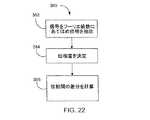
他の実施形態においては、これはフーリエ分解重ね合わせアルゴリズムを用いて達成され、これはグレーティング構造の周期的特徴を利用している。このアルゴリズムは、ターゲットパターンから得られた信号を一連のフーリエ高調波に分解する。グレーティングパターンの正規化ピッチに校正された異なるプロセスレイヤからの同じオーダーの高調波間の位相比較は、重ね合わせ計算の基礎としてはたらく。したがってこのアルゴリズムは、いくつかの独立した重ね合わせ結果−すなわちそれぞれのフーリエオーダーについて一つの結果を提供する。このアルゴリズムのフロー図は図22に示される。
【0140】
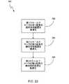
図21は、本発明のある実施形態によって共分散を用いて重ね合わせを計算する方法370を図示するフロー図である。例として、方法370は図20Aのステップ366に概ね対応する。方法370はステップ372で始まり、ここでは信号の相互相関が計算される。これは典型的には対向するワーキング・ゾーンについて行われる。図9のマークについて、信号の相互相関は、ワーキング・ゾーンのペア132A対反転された132D、132B対反転された132C、132E対反転された132H、および132F対反転された132Gについて計算される。信号の相互相関が計算されたあとで、プロセスフローはステップ374に進み、ここで相互相関の最大(サブピクセル)の位置が求められる。これは典型的にはレイヤの両方について、すなわちクロスハッチングで表されるレイヤ1、およびクロスハッチングなしで表されるレイヤ2についてなされる。相互相関最大の位置が求められたあと、プロセスフローはステップ376に進み、ここで相互相関の最大位置の間の差分を計算することによって重ね合わせが決定される。例えば、ワーキング・ゾーン132EおよびH(レイヤ1)−ワーキング・ゾーン132FおよびG(レイヤ2)の相互相関最大の間の差分は、X方向のミスレジストレーションを決定する。さらに、ワーキング・ゾーン132AおよびD(レイヤ1)−ワーキング・ゾーン132BおよびC(レイヤ2)の相互相関最大の間の差分は、Y方向のミスレジストレーションを決定する。
【0141】
図22は、本発明のある実施形態によってフーリエ分解を用いて重ね合わせを計算する方法380を図示するフロー図である。例として、方法380は図20Aのステップ366に概ね対応する。方法380はステップ382で始まり、ここで信号はフーリエ級数にあてはめられ、それらの位相が抽出される。あてはめられ、抽出されたあと、プロセスフローはステップ384に進み、ここで並置されたワーキング・ゾーン間の位相差が求められる。例えばY方向においては、位相差はワーキング・ゾーン132Aおよび132Bの間として求められ、同様にワーキング・ゾーン132Cおよび132Dの間として求められる。さらにX方向においては、位相差はワーキング・ゾーン132Eおよび132Fの間として求められ、同様にワーキング・ゾーン132Gおよび132Hの間として求められる。位相差が求められたあと、プロセスフローはステップ386に進み、ここで与えられた向きについての前のステップの位相差間の差分を計算することによって重ね合わせが決定される。例えばワーキング・ゾーン132EおよびFの位相差と、ワーキング・ゾーン132GおよびHの位相差との間の差分の平均はX方向におけるミスレジストレーションを決定する。さらにワーキング・ゾーン132AおよびBの位相差と、ワーキング・ゾーン132CおよびDの位相差との間の差分の平均はY方向におけるミスレジストレーションを決定する。レイヤの位置に対応するデータを得るために、位相差はピッチによって乗算され、2πによって除算される。
【0142】
要約すれば、上述の原則にしたがった重ね合わせマークを設計する方法がここで説明される。
【0143】
図23は、本発明のある実施形態によって重ね合わせマークを設計する方法390を図示するフロー図である。例として重ね合わせマークは上述のいかなるものにも概ね対応しえる。重ね合わせマークは一般に、基板の2つ以上の連続するレイヤ間、または基板の単一のレイヤ上の2つ以上別々に生成されたパターン間の相対的なズレを決定するために提供される。本発明のある実施形態によれば重ね合わせマークは、重ね合わせマークのパターンを形成する複数の要素を備えている。これら要素のそれぞれは、重ね合わせをより精密または正確に測定するための情報を含むように構成される。例として要素は、ワーキング・ゾーン、粗くセグメント化された要素および細かくセグメント化された要素の周期的構造に概ね対応する。
【0144】
方法390はステップ392で始まり、ここでマークの第1要素の幾何学的配置が第1スケールにしたがって最適化される。これは典型的には、第1スケールの上限および下限を求め、上限および下限間の第1幾何学的配置の幾何学的配置を微調整することによって達成される。ある実施形態においては、第1スケールは計測カーネルスケールに対応し、これは重ね合わせが測定される2つの異なるレイヤまたはパターンについての情報を含む領域の境界を規定する。計測カーネルスケールは、10ミクロンオーダーの特性寸法を持つ。例えば計測カーネルスケールは約4ミクロンから約10ミクロンの範囲であり、より具体的には約5ミクロンから約10ミクロンの範囲である。
【0145】
たいていの場合、計測カーネルスケールは計測ツール限界、プロセス問題、および回路設計条件に基づく。計測ツール限界は一般に計測ツールに関連した限界をいう(ラインのツール群およびライン内の特定のツール)。例えば計測ツール限界は、重ね合わせを測定するのに用いられる計測ツールの視野のサイズおよび形状、効果的に重ね合わせを測定するのに必要なターゲット領域の最小量、および計測ツールの要素によって生じる非対称収差および照明フィールド分布を含む。プロセスロバスト性問題は一般に、エッチング、成膜、機械化学研磨(CMP)のようなプロセスのロバスト性に関連した制限をいう。例えば、プロセスダメージおよびプロセスバラツキの影響をより受けやすいマークの部分が存在しえ、よってそれらは避けなければならない。回路設計条件は一般に、全体的な回路パターンを設計するのに用いられるルールをいう。例えば回路デザインルールは、重ね合わせマークバジェットに関するスクライブライン制限を含み、すなわちマークは典型的にはウェーハのスクライブライン内に位置する。スクライブラインは、ウェーハがソーイングまたはダイシングによって複数のダイに分割されるウェーハ上の場所である。
【0146】
いったん第1スケールが特定されると、重ね合わせが測定されるレイヤまたはパターンに関する情報を一般に含む第1要素の幾何学的配置が微調整され、このスケール内で最もうまく機能するマークレイアウトが見いだされる。ある実施形態においては、第1要素はワーキング・ゾーンに対応し、これは重ね合わせマークの異なるレイヤまたはパターンを規定し、かつ重ね合わせ測定に用いられる重ね合わせマークの実際の領域を表す。「幾何学的配置」という語は、第1要素、つまりワーキング・ゾーンのサイズ、形状および/または分布を一般にいう。ある実施形態においては、微調整はマークの周縁(例えばFOV)を規定すること、および重ね合わせの測定に対する非対称性の影響を最小限にするよう構成される複数のワーキング・ゾーンにマークを分割することによって実現される。例として、ワーキング・ゾーンは、結果として得られる重ね合わせ測定におけるツールに起因するズレに対する光学収差および照明の影響を最小化するように構成されえる。さらにワーキング・ゾーンは、結果として得られる重ね合わせ測定におけるウェーハに起因するズレに対するプロセスバラツキの影響を最小化するように構成されえる。
【0147】
第1要素の幾何学的配置が最適化されたあと、プロセスフローはステップ394に進み、ここでマークの第2要素の幾何学的配置が第2スケールにしたがって最適化される。これは典型的には、第2スケールの上限および下限を求め、上限および下限間の幾何学的配置を微調整することによって達成される。ある実施形態においては、第2スケールは画像解像度スケールに対応し、これは与えられたプロセスレイヤ内の構造間の境界を規定する。画像解像度スケールは、1ミクロンオーダーの特性寸法を持つ。例えば画像解像度スケールは約0.3ミクロンから約2ミクロンの範囲であり、より具体的には約0.5ミクロンから約1ミクロンの範囲である。
【0148】
たいていの場合、画像解像度スケールは計測ツール限界およびプロセスロバスト性問題に基づく。計測ツール限界は一般に計測ツールに関連した限界をいう(ラインのツール群およびライン内の特定のツール)。例えば計測ツール限界は、ツールの画像解像度、つまり画像をキャプチャする能力、重ね合わせ誤差を計算するためにツールによって用いられるアルゴリズム、およびツールの収差および照明フィールド分布を含む。プロセスロバスト性問題は、エッチング、成膜、機械化学研磨(CMP)のようなウェーハ上のレイヤおよびパターンを形成するのに用いられる材料およびプロセスによって生じる制限を一般にいう。例えば、アルミニウムコーティングされた化学機械研磨されたタングステンのような特定のプロセスについては、研磨およびアルミニウム成膜プロセスから生じる非対称性の影響を低減するために第2要素の幾何学的配置は1ミクロンまたはそれ未満であることが有利である。その他の場合には、金属粒度が大きいなら、線が1ミクロンよりも大きく、例えば2ミクロン程度までであることが望ましい。
【0149】
いったん第2スケールが特定されると、エンコードされ計測ツールに転送されるマーク要素相対位置に関する実際の空間情報を一般に含む第2要素の幾何学的配置が微調整され、このスケール内で最もうまく機能するマークレイアウトが見いだされる。ある実施形態において第2要素は、第1要素のワーキング・ゾーンのそれぞれの中に位置する粗くセグメント化された線の周期的構造に対応する。「幾何学的配置」という語は、第2要素、つまり粗くセグメント化された線の周期的構造(例えば線幅および間隔)を一般にいう。ある実施形態においては、粗くセグメント化された線を用いた周期的構造は、ツールの画像解像度をプロセスとバランス取ることによってかの測定を向上させるように構成される。
【0150】
第2要素の幾何学的配置が最適化されたあと、プロセスフローはステップ396に進み、ここでマークの第3要素の幾何学的配置が第3スケールにしたがって最適化される。これは典型的には、第3スケールの上限および下限を求め、上限および下限間の第3要素の幾何学的配置を微調整することによって達成される。ある実施形態においては、第3スケールはリソグラフィ解像度スケールに対応し、これは与えられた構造内のサブ構造の境界を規定する。リソグラフィ解像度スケールは、0.1ミクロンオーダーの特性寸法を持つ。例えばリソグラフィ解像度スケールは約0.01ミクロンから約0.5ミクロンの範囲であり、より具体的には約0.05ミクロンから約0.18ミクロンの範囲である。
【0151】
たいていの場合、リソグラフィ解像度スケールは、回路デザインルール、プロセスロバスト性問題および計測ツール限界に基づく。回路デザインルールは、全体的な回路パターンをデザインするのに用いられるルールを一般にいう。例えば回路デザインルールは、回路デバイスの幾何学的配置(例えば最小寸法サイズおよび密度)を含む。プロセスロバスト性問題は、エッチング、成膜、化学機械研磨(CMP)のようなウェーハ上のレイヤおよびパターンを形成するのに用いられる材料およびプロセスによって生じる制限を一般にいう。計測ツール限界は一般に計測ツールに関連した限界をいう(ラインのツール群およびライン内の特定のツール)。例えば計測ツール限界は、ツールのコントラスト要件、つまりより小さなサブ構造で構成されるより大きな構造を解像する能力を含みうる。
【0152】
いったん第3スケールが特定されると、回路構造そのものを反映する情報を一般に含む第3要素の幾何学的配置が微調整され、このスケール内で最もうまく機能するマークレイアウトが見いだされる。ある実施形態において第3要素は、第2要素の周期的構造の粗くセグメント化された複数の線を形成する細かくセグメント化された要素に対応する。「幾何学的配置」という語は、第3要素、つまり細かくセグメント化された要素のサイズ、形状および/または分布を一般にいう。ある実施形態においては、細かくセグメント化された要素は、プロセスの悪影響を最小限にするよう構成されることで、重ね合わせ測定の正確するおよび精密さを改善する。他の実施形態においては、前に図3〜5で説明したように、ターゲットおよび実際のデバイス間でのステッパPPEのバラツキを最小化するように構造は最適化される。
【0153】
本発明はいくつかの好ましい実施形態について説明されてきたが、本発明の範囲に含まれる改変、組み合わせ、および等価物が存在する。
【0154】
例えば、本発明は半導体デバイス製造について説明されてきたが、本発明は、100nm露光波長にまで下がるフォトリソグラフィ、波長が10nmから100nmの極紫外線リソグラフィ、波長が10nmより小さいX線リソグラフィ、電子ビームリソグラフィ、イオンビームパターニング、またはこれらの複数の方法を用いた混合リソグラフィを含む、光学または光電子工学デバイスの微小製造、磁気記憶媒体または磁気記憶書き込み/読み出しまたは入力/出力デバイスの微小製造、リソグラフィパターニング一般を用いた微小製造のような、他のタイプのデバイスを製造するのにも適していることに注意されたい。
【0155】
さらに重ね合わせ測定のデータを供給する以外にも、周期的構造ターゲットは、ターゲット、ステッパおよび計測ツールの診断のための多くの追加情報(例えばコントラスト、シャープさ、粒度、捕捉クオリティおよび対称性測定基準)を提供することができる。例えば共分散およびフーリエ分解方法によって得られた重ね合わせの比較、精度、TIS、およびTISの変化の結果はそのような機械として機能する。同じ信号からの異なるフーリエ高調波間の位相差の測定によって、プロセス不完全性、収差または照明問題によるマークの対称性に関する重要な情報が得られる。180度だけ回転されたターゲットについて同じ分析を実行することによって、ウェーハの非対称性を計測ツールによるそれらから分離することが可能である。ターゲット構造によるFOV全体を埋めることによって、異なるワーキング・ゾーンを選択することができ、よって単一のターゲット内でのバラツキに関する情報を提供することができ、追加の最適化も可能になる。最後にグレーティングターゲットは、FOVにおけるターゲットのチルトのより簡単な診断のための機会を提供する。
【0156】
さらに、情報の1次元アレイを利用するとしてアルゴリズムが説明されてきたが、それらはまた情報の2次元アレイにも適用可能であることに注意されたい。
【0157】
さらに、マークは重ね合わせを測定するためにここでは説明されてきたが、それらは1以上の以下の測定または応用のために用いられてもよい。すなわちCD、露光モニタリング、レジストプロファイルモニタリング、フォーカスモニタリングなど。
【0158】
本発明による方法および装置を実現するには多くの代替方法が存在することに注意されたい。よって以下に添付の特許請求の範囲は、そのような改変、組み合わせ、および等価物も本発明の真の精神および範囲に入るとして解釈されるべきであると意図するものである。
【図面の簡単な説明】
【図1A】従来の重ね合わせマークの上から見た平面図である。
【図1B】従来の重ね合わせマークの上から見た平面図である。
【図2】本発明のある実施形態による重ね合わせマークの上から見た平面図である。
【図3】本発明のある実施形態による細かくセグメント化された周期的構造の部分側面立面図である。
【図4】本発明のある実施形態による細かくセグメント化された周期的構造の部分側面立面図である。
【図5A】本発明のある実施形態による細かくセグメント化された周期的構造の部分側面立面図である。
【図5B】本発明のある実施形態による細かくセグメント化された周期的構造の部分側面立面図である。
【図6】本発明の他の実施形態による重ね合わせマークの上から見た平面図である。
【図7】本発明の他の実施形態による重ね合わせマークの上から見た平面図である。
【図8】本発明の他の実施形態による重ね合わせマークの上から見た平面図である。
【図9】本発明の他の実施形態による重ね合わせマークの上から見た平面図である。
【図10】本発明の他の実施形態による重ね合わせマークの上から見た平面図である。
【図11】本発明の他の実施形態による重ね合わせマークの上から見た平面図である。
【図12】本発明の他の実施形態による重ね合わせマークの上から見た平面図である。
【図13】本発明の他の実施形態による重ね合わせマークの上から見た平面図である。
【図14】本発明の他の実施形態による重ね合わせマークの上から見た平面図である。
【図15】本発明の他の実施形態による重ね合わせマークの上から見た平面図である。
【図16】本発明の他の実施形態による重ね合わせマークの上から見た平面図である。
【図17】本発明の他の実施形態による重ね合わせマークの上から見た平面図である。
【図18】本発明の他の実施形態による重ね合わせマークの上から見た平面図である。
【図19】本発明のある実施形態による重ね合わせ測定システムの簡略化された概略図である。
【図20A】本発明のある実施形態によって重ね合わせを計算する方法を図示する簡略化されたフロー図である。
【図20B】本発明のある実施形態による図9の重ね合わせマークの上から見た平面図である。
【図20C】本発明のある実施形態による折り畳まれた1次元信号のペアを示す図である。
【図21】本発明のある実施形態によって共分散を用いて重ね合わせを計算する方法370を図示するフロー図である。
【図22】本発明のある実施形態によってフーリエ分解を用いて重ね合わせを計算する方法380を図示するフロー図である。
【図23】本発明のある実施形態によって重ね合わせマークを設計する方法のフロー図である。
【符号の説明】
10…ターゲット
12…内側ボックス
14…外側ボックス
70…マーク
71…周縁
72…ゾーン
72…ワーキング・ゾーン
74…周期的構造
76…線群
78…要素
79…FOV
80…除外ゾーン
81…ダークフィールド
82…クリアフィールド
84…第1周期的構造
85…第2周期的構造
90…マーク
92…ワーキング・ゾーン
94…周期的構造
96…追加構造
100…マーク
102…ワーキング・ゾーン
104…周期的構造
106…線
108…追加構造
110…マーク
112…ワーキング・ゾーン
114…周期的構造
116…要素
118…要素
130…マーク
132…ワーキング・ゾーン
133…除外ゾーン
134…第1ワーキング・グループ
136…第2ワーキング・グループ
138…周期的構造
140…マーク
144…FOV
150…マーク
152…要素
170…マーク
172…ワーキング・ゾーン
174…周期的構造
176…線
178…追加構造
178…要素
190…マーク
192…ワーキング・ゾーン
193…除外ゾーン
194…ワーキング・グループ
194…第1ワーキング・グループ
196…第2ワーキング・グループ
198…周期的構造
200…線群
210…マーク
212…グレーティングパターン
214…線
220…マーク
222…ワーキング・ゾーン
240…マーク
242…ワーキング・ゾーン
250…マーク
252…ワーキング・ゾーン
270…マーク
272…ワーキング・ゾーン
290…マーク
292…ワーキング・ゾーン
320…測定システム
322…ターゲット
324…ウェーハ
326…光学アセンブリ
328…コンピュータ
330…光源
332…光
334…第1パス
335…第1レンズ
336…光ファイバライン
338…第2レンズ
340…ビームスプリッタキューブ
342…パス
344…対物レンズ
346…パス
350…チューブレンズ
352…カメラ
354…フレームグラバ
356…ウェーハステージ[0001]
FIELD OF THE INVENTION
The present invention relates generally to overlay measurement techniques used in semiconductor manufacturing processes. More specifically, the present invention relates to overlay marks for measuring alignment errors between different layers of a semiconductor wafer stack or different patterns on the same layer.
[0002]
BACKGROUND OF THE INVENTION
Measurement of the overlay error of patterned successive layers on a wafer is one of the most important control techniques used in the manufacture of integrated circuits and devices. The overlay accuracy is generally determined by how accurately the first pattern layer aligns with the second pattern layer located above or below, or the second pattern where the first pattern layer is located on the same layer. Regarding how accurately to align the layers. Currently, overlay measurements are made via test patterns printed with the layers of the wafer. Images of these test patterns are captured via an imaging tool and an analysis algorithm is used to calculate the relative displacement of the patterns from the captured images.
[0003]
The most commonly used overlay target pattern is a "box-in-box" target, which comprises a pair of concentric squares (or rectangles) formed on successive layers of a wafer. The overlay error is generally determined by comparing the position of one square to another.
[0004]
1A is a top view of a typical “box-in-box”
[0005]
"Box in bar" and "bar in bar" were also introduced. These are generally the same shape as "box-in-box". In the "box in a bar" target, the outer box of the "box in box" is separated into multiple parallel bars (see FIG. 1B). In the "bar-in-bar" overlay mark, both the outer and inner boxes of the "box-in-box" target are separated into multiple parallel bars. Further examples of this type of modified target are taught in U.S. Patent No. 6,118,185 to Chen et al.
[0006]
Recently, separate bars have been introduced to create patterns comparable to the design rules of the device itself. For example, U.S. Patent No. 6,130,750 to Ausschnitt et al. Discloses a "box-in-box" type target with separate bars.
[0007]
Although such designs work, there is an ongoing effort to provide targets with improved functionality. For example, it is desirable to provide a target that can improve the correlation between the overlay error measured on the test pattern and the actual overlay error of the circuit element.
[0008]
Summary of the Invention
The invention relates, in one embodiment, to an overlay mark that determines a relative shift between two or more successive layers of a substrate. The overlay mark includes at least one test pattern that determines a relative displacement between the first and second layers of the substrate in a first direction. The test pattern includes a first set of working zones and a second set of working zones. A first set of working zones is disposed on the first layer of the substrate and has at least two diagonally opposed working zones spatially offset from one another. A second set of working zones is disposed on the second layer of the substrate and has at least two diagonally opposed working zones that are spatially offset from one another. The first set of working zones is generally angled with respect to the second set of working zones, thus forming an "X" shaped test pattern.
[0009]
The invention relates, in another embodiment, to an overlay mark that determines the relative misalignment between two or more successive layers of a substrate using an imaging device configured to capture an image of the overlay mark. . The overlay mark includes a first set of working zones located on a first layer of the substrate. The first set of working zones includes at least two working zones that are diagonally opposed and are located within the periphery of the mark. Each of the working zones includes a periodic structure of coarsely segmented elements located therein. The coarsely segmented element is generally oriented in the first direction. The overlay mark further includes a second set of working zones that are positioned diagonally with respect to the first working group. The second working group is disposed on the second layer of the substrate and includes at least two working zones diagonally opposite each other and located within the periphery of the mark. Each of the working zones includes a periodic structure of coarsely segmented elements located therein. The coarsely segmented element is generally oriented in the first direction.
[0010]
The invention, in another embodiment, relates to an overlay mark that determines the relative shift between two or more separately generated patterns on a single layer of a substrate. The overlay target includes a test area located on a first layer of the substrate. The first layer is typically formed by a first pattern using a first process and a second pattern using a second process. The overlay target further includes a plurality of working zones located in the test area. The working zone represents the actual area of the test area used to determine the relative deviation between the first and second patterns. A first portion of the working zone is formed using a first process, and a second portion of the working zone is formed using a second process. The overlay target further includes a periodic structure located within each of the working zones. Each of the periodic structures includes a plurality of coarsely segmented elements. Each of the coarsely segmented elements is formed by a plurality of finely segmented elements.
[0011]
The invention, in another embodiment, relates to a method for determining the relative deviation between two or more consecutive layers of a substrate or between two or more separately generated patterns on a single layer of a substrate. . The method includes capturing an image of an overlay mark formed on a substrate. The overlay mark has multiple working zones. Each of the working zones contains a periodic structure of coarsely segmented elements. The method further includes selecting a plurality of working zones from the captured image, wherein at least one working zone from each layer or pattern is selected. The method further includes forming a signal with information for each of the selected working zones, wherein at least one signal is formed for each layer or pattern. The method also includes determining the relative shift between different layers or patterns by comparing the signal from a first layer or pattern with a signal from a second layer or pattern.
[0012]
The present invention relates, in one embodiment, to an overlay mark that determines the relative misalignment between two or more consecutive layers of a substrate, or between two or more patterns generated separately on a single layer of the substrate. About. The overlay mark includes a plurality of working zones, which are used to calculate the alignment between the first and second layers of the substrate or between the first and second patterns on a single layer of the substrate. Each of the working zones is located within the periphery of the mark. Each of the working zones represents a different area of the mark. The working zone is configured to substantially fill the perimeter of the mark such that the combined area of the working zone is substantially equal to the total area of the mark.
[0013]
The invention is used, in one embodiment, to determine the relative misalignment between two or more successive layers of a substrate, or between two or more patterns generated separately on a single layer of a substrate. And a method for designing a registration mark to be formed. The method includes optimizing a geometric arrangement of a first element of the mark according to a first scale. The method further includes optimizing a geometry of the second element of the mark according to the second scale. The method further includes optimizing the geometry of the third element of the mark according to a third scale.
[0014]
The invention, in another embodiment, relates to a method of designing an overlay mark. The overlay mark has a periphery corresponding to the field of view of the measurement tool. The method includes filling the periphery of the registration mark with a plurality of working zones. The working zone geometry is based on the first design scale. The method further includes filling each of the working zones with at least one periodic structure of coarsely segmented lines. The geometry of the coarsely segmented line is based on a second scale that is smaller than the first scale. The method further includes dividing the coarsely segmented line into a plurality of finely segmented elements. The geometry of the finely segmented element is based on a third scale that is smaller than the second scale.
[0015]
The invention, in another embodiment, relates to a method of designing an overlay mark. The method includes defining a perimeter of the registration mark. The method further includes dividing the registration mark into a plurality of working zones. The working zones include at least a first working zone associated with a first process and at least a second working zone associated with a second process. The second process has different properties than the first process. The method further includes adjusting the working zone geometry. The geometry of the working zone is based at least in part on a first scale. The method further includes locating the periodic structure within each of the working zones. The periodic structure has a plurality of coarsely segmented lines. The method further includes adjusting the geometry of the periodic structure. The geometry of the periodic structure is based at least in part on a second scale. The second scale has different characteristics from the first scale. The method further includes dividing the coarsely segmented line into a plurality of finely segmented elements. The method further includes adjusting the geometry of the finely segmented elements. The geometry of the finely segmented line differs at least in part from the first and second scales.
[0016]
The invention, in another embodiment, relates to an overlay that determines the relative misalignment between two or more consecutive layers of a substrate, or between two or more patterns generated separately on a single layer of a substrate. About the mark. The overlay mark includes a plurality of coarsely segmented lines formed by a plurality of finely segmented bars and at least one dark field. The plurality of coarsely segmented lines are separated by a plurality of finely segmented bars and at least one clear field.
[0017]
The invention, in another embodiment, relates to an overlay that determines the relative misalignment between two or more consecutive layers of a substrate, or between two or more patterns generated separately on a single layer of a substrate. About the mark. The overlay mark is formed by a plurality of finely segmented bars and includes a first group of coarsely segmented lines separated by a clear field. The overlay mark is further formed by a plurality of finely segmented bars and includes a second group of coarsely segmented lines separated by dark fields.
[0018]
The present invention, in one embodiment, determines, via scanning, the relative misalignment between two or more consecutive layers of a substrate, or between two or more patterns generated separately on a single layer of a substrate. The overlay mark to be performed. The overlay mark includes at least one test pattern that determines a relative displacement between the first and second layers of the substrate in a first direction. The test pattern has a first set of working zones and a second set of working zones. The first set is disposed on a first layer of the substrate and has at least two working zones diagonally opposed and spatially offset from one another. The second set is disposed on the second layer of the substrate and has at least two working zones diagonally opposed and spatially offset from one another. The first set of working zones is generally angled with respect to the second set of working zones, thereby forming an "X" shaped test pattern.
[0019]
The present invention, in another embodiment, provides an overlay mark that determines a relative shift between two or more successive layers of a substrate via an imaging device configured to capture an image of the overlay mark. About. The overlay mark includes a first set of working zones located on a first layer of the substrate. The first set of working zones includes at least two working zones that are diagonally opposed and spatially offset from one another and are located within the perimeter of the mark. Each of the working zones has a periodic structure of coarsely segmented elements located therein. The coarsely segmented element points in the first direction. The overlay mark further includes a second set of working zones located at an angle to the first working group. A second working group is disposed on the second layer of the substrate and has at least two working zones located diagonally opposite and spatially offset from one another and located within the perimeter of the mark. Each of the working zones has a periodic structure of coarsely segmented elements located therein. The coarsely segmented element points in the first direction.
[0020]
The present invention has been described by way of example and not limitation.
[0021]
BEST MODE FOR CARRYING OUT THE INVENTION
The present invention will be described in detail with reference to some preferred embodiments thereof, which are illustrated in the accompanying drawings. In the following description, numerous specific details are set forth in order to provide a thorough understanding of the present invention. It will be apparent, however, to one skilled in the art, that the present invention may be practiced without some or all of these specific details. In other instances, well known process steps have not been described in order not to unnecessarily obscure the present invention.
[0022]
In each of the various embodiments, the present invention employs an overlay mark comprising a periodic structure formed on each of the two layers of the semiconductor wafer, thereby providing an overlay between the two layers of the semiconductor device. Provide information. When the two layers are properly aligned by the formation of overlay marks at specific locations on each wafer layer, the periodic structure on one layer is aligned with the periodic structure on another layer. Conversely, when the two layers are not properly aligned, the periodic structures on each layer will deviate from each other. Alternatively, the present invention may use overlay marks consisting of periodic structures formed on a single layer by two or more different processes to provide alignment information between two different patterns on the same layer. Good. Each of the periodic structures is composed of multiple structures, which can be significantly modified to increase the amount of information used to measure the overlay and to reduce the effect of certain processes on the overlay measurement. Each of these measurements consists of substructures of approximately the same size and spacing (or distance) as the structure of the actual integrated circuit. By forming each of the periodic structures with substructures sized close to the actual circuit size, any alignment errors in such circuits can be measured more accurately. The invention is particularly suitable for overlay measurement techniques where it is necessary to capture an image of the overlay mark.
[0023]
The periodic structures and substructures described herein are generally patterned using appropriate photolithographic techniques, and the lithographic patterns are then patterned using other process materials, such as etching and deposition, with other materials and layers. Is transferred to In the simplest application, the transferred pattern constitutes an etched or deposited wire or via. For example, the periodic structures and substructures may be formations of photoresist material in the wafer layer, recessed cavity formations, buried trenches and / or other structures. The structures and substructures formed by the cavities can be cavities formed in any layer during the semiconductor manufacturing process. For example, the cavities can be formed in a photoresist layer, a dielectric material layer, or a metal layer. Note that the above process is not limiting and any suitable manufacturing technique may be used.
[0024]
Embodiments of the present invention will be described below with reference to FIGS. However, as will be appreciated by those skilled in the art, the detailed description set forth herein for these figures is for illustrative purposes and the invention is broader than these limited embodiments.
[0025]
FIG. 2 is a top plan view of an
[0026]
The
[0027]
It is generally considered that the
[0028]
The
[0029]
In many cases, the working zones 72 are spatially separated from each other so that they do not overlap portions of adjacent working zones (ie, each of the working zones defines a different area of the mark). Represent). This is typically done to ensure that each of the working zones is properly imaged by the metrology tool. Although not always necessary, working zones 72 may be spatially separated by
[0030]
In some embodiments, the geometry, including the size, shape, and distribution of the working zones, is configured to balance or compensate for any non-uniformity or asymmetry characteristics that may occur across the mark. Asymmetry can arise from optical aberrations and illuminance asymmetries (displacement due to the tool) in the metrology tool, as well as structural features due to the process (displacement due to the wafer).
[0031]
Tool-induced offset (TIS) generally refers to how the apparent position of a mark moves or shifts as a result of metrology tool issues such as non-uniform illumination and / or optical aberrations. Illuminance generally relates to how that light is distributed to the target. Aberration relates to how the light converges and is collected. Non-uniform illumination can be caused by defects or misalignment in one of the optical elements with respect to the transmission of light from the light source to the wafer. Non-uniform optical aberrations can be caused by defects or misalignments in the objective lens of the optical system. Aberrations include, by way of example, spherical aberration, astigmatism and coma. Coma can have a greater effect on the TIS due to its asymmetry nature across the FOV of the metrology tool.
[0032]
Wafer-induced misalignment (WIS) generally refers to how much the apparent position of a mark moves or shifts as a result of process variations such as the strain caused by chemical mechanical polishing (CMP) and sputter deposition.
[0033]
Non-uniformities, asymmetries, and variations may also result from differences between the heights of different wiring sets in each layer. Lower layer interconnects are sometimes only visible through intermediate layers of the wafer. This is because the material of the intermediate layer covers the wiring of the lower layer. The upper interconnect, on the other hand, is typically formed from photoresist applied over the lower layer.
[0034]
Thus, by adjusting the size, shape and distribution of the overlay information from the two layers or patterns in the field of view of the overlay metrology tool, the effects of lithography and / or process non-uniformities, asymmetries, and variations are reduced. It is possible to do. In some cases, it is even possible to improve the overlay measurement. Resist patterns are less susceptible to process variations, so they are potentially more useful as capture areas for marks.
[0035]
In some embodiments, balancing is achieved by selectively placing working zones of the same layer at different locations near the periphery of the mark. For example, working zones can be located at different locations within the FOV to obtain the best possible balance between aberrations that vary across the FOV, illumination and process results. In the illustrated embodiment (FIG. 2), the working zones of the same layer are arranged opposite to each other, which occurs from left to right, from top to bottom or from inside to outside of the FOV (reverse case). ) Can be balanced. In some implementations, the optimal distribution to balance the asymmetry is the optics of the shift due to the tool (eg, how the apparent position of the mark moves as a result of tool issues such as illumination and / or aberrations). Is determined by performing a dynamic simulation. In other implementations, the optimal distribution for balancing asymmetry is determined by performing an experiment (eg, running a sample of a wafer). In addition, portions of the mark that have unacceptable aberrations and illumination and / or process damage may be present in the FOV, so that the working zones are located at specific locations in the FOV to avoid these areas. I can.
[0036]
As described above, each of the working zones is configured to represent one of two consecutive layers of the overlay mark. In some embodiments, the working zones represent a number equal to the first layer or pattern and the second layer or pattern, ie, for each working zone of the first layer, the second layer has a corresponding working zone. Zone exists. This is typically done to balance variations, non-uniformities, and / or asymmetries present in the layers and / or metrology tools. Thus, the number of working zones is generally based on a factor of two, for example, 2, 4, 8, 16. It is generally believed that by distributing the area to more points in the field of view, illumination, aberrations and non-uniformities caused by the process can be better balanced. For example, the size (square) of the working zone is generally about 2 to about 24 microns, and more specifically, about 4 to about 15 microns. In many cases, the size of a working zone is inversely proportional to the number of working zones, that is, the size decreases as the number increases. By way of example, the size of the working zone is generally about 10 to about 24 microns for a 4 working zone, about 5 to about 12 microns for an 8 working zone, and for a 16 working zone, From about 2.5 to about 6 microns.
[0037]
Further, there may be cases where the number of working zones of the first and second layers need to be unequal, such as four first layer working zones and two second layer working zones. There may also be cases where the total number of working zones needs to be unequal, such as two first layer working zones and one second layer working zone. There may also be cases where the sizes of the working zones need to be unequal. For example, a first group of working zones has a first size, and a second group of working zones has a second size, where the second size is smaller or larger than the first size.
[0038]
The working zone is generally constrained by the FOV (eg, the perimeter of the mark), but the shape of the working zone can be varied depending on the specific requirements of each mark. By way of example, the zones may be square (as shown), L-shaped, rectangular, triangular, circular, polygonal, etc. In many cases, the shape and size of the working zones are the same. This is typically done to balance the variability, non-uniformity and / or asymmetry present in the layers and / or metrology tools. It should be noted, however, that this is not a limitation and that some or all of the working zones may have different shapes. For example, some working zones may be rectangular in shape, and other working zones may be square in shape.
[0039]
Further, working zones representing different layers are typically juxtaposed to one another. By way of example, a mark may include at least two juxtaposed working zones. That is, a right area representing the first layer and a left area representing the second layer. Further, the mark may include an upper working zone representing the first layer and a lower working zone representing the second layer. In some embodiments, the juxtaposed regions are positioned equidistant from the center of the target (ie, the center of the FOV). It should be noted, however, that the juxtaposition is not a limitation, and the location of the working zone can be varied according to the specific requirements of each mark. For example, there may be cases where a working zone representing the first layer needs to be juxtaposed to another working zone representing the first layer.
[0040]
Referring to FIG. 2, working
[0041]
Note that this particular "X" configuration is shown for purposes of illustration and not limitation. That is, the size, shape and distribution of the working zone and its periodic structure can vary according to the specific requirements of each mark. For example, the working zones may be configured to fill different FOVs of different sizes and different shapes. It is generally desirable to fill the field with as much information as possible for reasons of process robustness and information optimization. The working zone may also take other shapes such as rectangles, triangles, parallelograms, trapezoids, regular polygons, circles and the like. Further, opposing periodic structures may be provided on other layers. For example, the working
[0042]
Each of the working zones 72 includes an individual
[0043]
Although some of the finely segmented
[0044]
In some embodiments, the geometry of the periodic structure, ie, line width and spacing, is configured to find an appropriate balance between the image resolution of the metrology tool and the robustness of the process. For example, it is often desirable to have large geometries (eg, large line widths and spacings) so that periodic structures are optically resolved by the tool, while smaller geometries (eg, small lines). Width and spacing) to minimize process impact on the mark. With respect to image resolution, there is a minimum size requirement that each metrology tool has to resolve coarsely segmented lines. It is generally known that as the period of the periodic structure decreases, the resolution of the measurement tool decreases, that is, there is a point where the resolution of the measurement tool does not work effectively. With respect to process robustness, there are certain effects on overlay marks each time a new process is introduced into semiconductor manufacturing. The ability to measure a target depends on its field of view or contrast in the imaging tool. Some processes, such as metallization, tend to reduce contrast and thus affect accuracy. Other processes, such as chemical mechanical polishing (CMP), tend to blur or distort the marks, thus affecting accuracy. These processes also asymmetrically structure or create an apparent, optically measured spatial counterpart to the center of the originally patterned trench or wiring (eg, circuit pattern).
[0045]
For certain processes, such as tungsten coated with aluminum and chemically mechanically polished, the characteristic dimensions of these structures are approximately 1-2 microns to reduce the effects of asymmetry arising from the polishing and aluminum deposition processes. Advantageously, However, if the width of the trench is too small, the remaining topography on top of the aluminum layer is too small to provide optically appropriate contrast and thus the mark does not provide proper overlay information. On the other hand, the lower limit for the feature size of the structure at this scale is determined by the resolution limit of the metrology tool. For example, for a superposition tool with a numerical aperture (NA) of 0.9 and an average illumination wavelength of 550 nm, the Rayleigh resolution limit or reference will be approximately 0.4 microns. In this particular case, it is preferable to keep the line width 0.5 micron in order not to reduce contrast and hence signal-to-noise, and to reduce the effect of asymmetry arising from polishing and aluminum deposition processes. Preferably, it is kept below ~ 2 microns. Note, however, that this is by way of example and not by way of limitation, it is possible to achieve better than the Rayleigh resolution limit.
[0046]
In some embodiments, the geometry of the periodic structure is determined empirically. To find the period in which the change in TIS is minimal, i.e., to select the pitch that minimizes the TIS change and process change by measuring the change in tool-induced offset at multiple locations on the wafer, For example, some wafers go through the process
[0047]
In some embodiments, the period and phase of the periodic structure are configured to filter high frequency edges.
[0048]
In the illustrated embodiment, each of the
[0049]
The equal period, line width and spacing for each of the periodic structures is not a limitation, and they can be varied according to the specific requirements of each mark. For example, each of the periodic structures may have a different period or duty cycle. Alternatively, some of the periodic structures may have equal periods or duty cycles, while other periodic structures may have different periods or duty cycles. Further, the periodic structure may have a period that varies over the periodic structure. By way of example, the periodic structure may be a chirped periodic structure (eg, from small to large). As mentioned above, the period, line width and spacing are generally optimized according to the process robustness and contrast requirements of the metrology tool.
[0050]
The number of lines within each periodic structure can be varied to meet the specific requirements of each mark. It is generally assumed that the number of lines depends on the required resolution and the desired signal to noise ratio. Most imaging tools have a resolution limit between about 0.3 and about 0.9. The number of lines is also determined by process requirements, such as chemical mechanical polishing strain, which affect the outermost line segments of the group more than the inner line segments. One factor that affects the maximum number of lines used in a group of line segments is the resolution of the metrology tool. In terms of the minimum number of lines required for operation, that number is two. In the illustrated embodiment, each of the
[0051]
In the illustrated embodiment, the lines of the
[0052]
In some embodiments, the overlay alignment between layers can be determined by calculating the center of symmetry of each of the opposing regions on the same layer, and then calculating the difference between the two averaged centers of symmetry. . For example, the centers of symmetry for both working
[0053]
Alternatively, groups of periodic structures parallel to each other and on different layers are compared. That is, the
[0054]
Note that measuring overlay in the X direction is not a limitation, and
[0055]
Furthermore, if the solid lines are printed on the first layer of the semiconductor wafer and the solid lines are on the second layer, another set of lines on the third layer Note that the group (shown here as a solid outline) may be printed over the first layer line group. At this time, the line group of the second layer is used in association with the line group of the third layer. Thus, each set of lines on the layer of the semiconductor wafer (except those on the first and last layers) is a line group on two layers of the semiconductor wafer, one above and one below. Used in conjunction with This implementation works best if the first layer is below the third layer and is not optically detectable. Alternatively, if there is sufficient space on the semiconductor wafer surface, the grating pairs of each pair of adjacent layers on the wafer can be located at different locations on the wafer to measure the two top layers of interest. Can be minimized from the third layer.
[0056]
More specifically, the finely segmented
[0057]
One reason smaller overlay marks provide a more accurate overlay measurement is that smaller sized finely segmented elements are more similar to lens pattern placement errors that occur when integrated circuit patterns are formed. This is because it is formed on the semiconductor layer together with the lens pattern arrangement error. The pattern is formed on the wafer layer with a lithographic apparatus such as a "stepper". Lens placement errors in patterns formed on semiconductor wafers vary with pattern size and spacing due to aberrations in the stepper lens, and the illuminance used to expose circuit patterns defined on the lithographic mask. Varies with conditions, including off-axis illumination and partial coherence. Creating marks having a minimum size and pitch comparable to that of the integrated circuit element's critical dimensions is achieved by using mask pattern technology that is the same or similar to the minimum dimensions of the circuit (eg, the same or similar optical proximity correction or phase). Using a shift mask pattern) will produce marks and integrated circuit patterns that are formed with a more similar degree of lens pattern placement error. Thus, alignment between marks on different layers of the wafer more accurately represents alignment between circuit patterns. For more information on distortion due to stepper lens aberration, see Harry J. et al. See Lithography Process Control by Levinson.
[0058]
In some embodiments, the minimum dimension size and pitch of the finely segmented elements (e.g., the distance between the centers of the finely segmented elements) is the critical device minimum of the patterning step performed on the layer being tested. Substantially equal to those of the dimensions. That is, the dimensions of the finely segmented
[0059]
Another reason smaller overlay marks provide more accurate overlay measurements is because the effect of wafer manufacturing asymmetry on overlay measurements is reduced. Wafer fabrication asymmetry is that the shape and size of the structures or patterns formed on the wafer layer will shift due to further processing. The impact of the wafer fabrication process on the overlay marks depends on the size, spacing, and density of the overlay mark structures and substructures. These deviations in shape and size affect overlay marks and reduce the accuracy of overlay measurements.
[0060]
An exemplary wafer fabrication technique that produces an asymmetric profile in a wafer structure is a sputter deposition process. Sputtering processes are commonly used to apply a layer of material (ie, metal) over an existing wafer layer. Typically, the source of material to be sputtered, the target, is located above the center of the wafer. The material to be sputtered moves from the target toward the outer edge of the wafer, thereby causing an asymmetric deposition of the material in the concave channel or on the ridge-like protrusions. Specifically, non-uniform accumulation of deposited material between the sidewalls of a dented channel can shift the apparent position of the concave channel to one side of the channel.
[0061]
Another exemplary manufacturing technique that can produce asymmetric dimensions is mechanical layer planarization (CMP) of the wafer layer. Under certain circumstances, a wafer layer undergoes CMP before the next layer of material is deposited. CMP equipment typically moves in a particular orientation across the wafer layer. Thus, the CMP apparatus first encounters one side of the overlay mark and then moves to the opposite side of the mark. This causes a displacement of the overlay mark and a change in apparent size. This is because more material on the side of the registration mark that is first encountered may be removed than on the opposite side of the mark.
[0062]
In either situation, the resulting asymmetry of the overlay mark in the manufacturing process can be reduced by forming smaller marks. With respect to the sputtering process, the smaller the concave channels or ridges, the less sputter material will accumulate on each sidewall surface, thereby resulting in a smaller shape and size asymmetry shift. With respect to the CMP process, marks with smaller dimensions still shift to a lesser degree. Conversely, there are process situations where the overlay mark line is broadened to be more robust to process changes, such as in the case of large grain metal layers. For more detailed information, see Harry J. et al. See Lithography Process Control by Levinson.
[0063]
In the illustrated embodiment, the finely segmented
[0064]
Further variations include elements of various shapes formed within a single overlay mark. For example, one periodic structure may include linear shaped elements, while another periodic structure may include circular shaped elements. Further, some periodic structures may include circular shaped elements, while other periodic structures may include square shaped elements. Further, some periodic structures may include linear shaped elements, while other periodic structures may include square shaped elements. Still further variations include elements of various shapes formed within a single periodic structure. For example, a single periodic structure may include one coarsely segmented line formed by linear shaped elements and another coarsely segmented line formed by square shaped elements. Further variations include periodic structures composed of finely segmented elements and some periodic structures not composed of finely segmented elements but composed of a single thick line.
[0065]
Referring to FIG. 3, the finely segmented
[0066]
It has been found that stepper aberrations like coma (as opposed to metrology tool aberrations) can cause apparent overlay errors when the overlay mark is finely segmented. That is, in addition to having a tendency to introduce pattern placement errors, stepper coma also measures the dimensions of the finely segmented elements, especially the first and last bars (eg, bars 78 'and 78 ") that make up the coarsely segmented line "Resize" generally means that the first and last bars can be narrower or wider. Often, when one bar becomes wider, the other bar becomes narrower. For example, coma makes the last bar wider and the first bar thinner. This can also be caused by the presence of bars near the open spaces between the coarsely segmented lines. As will be appreciated, this type of change tends to introduce an apparent misalignment (ie, the lines appear to shift from left to right), and thus the lines are not measured correctly. In some embodiments, the layout of the periodic structure may be reconfigured to compensate for this apparent shift (see FIGS. 4 and 5).
[0067]
In lithography, a clear field generally refers to a series of periodic structures surrounded by open spaces (eg, etched), and a dark field generally refers to a series of periodic structures surrounded by closed spaces (eg, unetched). Refers to a periodic structure. Clear fields generally appear brighter and dark fields generally appear darker. In this particular embodiment, the clear field is the open space between groups of finely segmented elements, such as the bars of FIG. 3, and the dark field is the finely segmented elements, such as the bars of FIG. Is a closed space between groups. It is generally believed that the clear and dark fields can be configured to alter the formation of the lines so that the apparent misalignment caused by the widened and thinned bars is canceled or unbalanced. In some implementations, a balance is achieved within each periodic structure. For example, each of the working zones includes a fine segment with both clear and dark fields. For example, some coarsely segmented lines have clear fields and some have dark fields. In another implementation, a balance is made between two periodic structures in different working zones. For example, at least a first working zone includes a periodic structure having fine segments with a clear field, and at least a second working zone includes a periodic structure with fine segments with a dark field. In most cases, the first and second working zones are opposing working zones on the same layer. These implementations are described in detail below with reference to FIGS.
[0068]
FIG. 4 is a partial side elevational view of any of the
[0069]
5A and 5B are partial side elevational views of two separate
[0070]
Referring to FIG. 5A, the first
[0071]
As can be seen from the above description, the X-shaped configuration has many effects. For example, an X configuration provides more information than a standard box-in-box target that fills the periphery of the mark from center to edge. Increasing the number of edges (eg, coarsely segmented lines) along with their length also provides more information. Apart from providing more information by increasing the number of edges and their length, the X-shape has more effect than a regular box-in-box target, thanks to the additional symmetry inherent in it. provide. That is, in a normal box-in-box structure, there are inner and outer layers. When they are interchanged, they result in different patterns due to the different information distribution of the inner and outer marks, and the different optical behavior of the metrology tool in areas near and far from the center of the field of view, thus resulting in different overlay results. Spawn. From this point, the X-shaped target structure is basically invariant with respect to layer switching (up to mirror image conversion). In addition, the X configuration helps to overcome the asymmetric coma pattern, that is, exhibits a 180 degree rotational symmetry where the coma aberration cancels out.
[0072]
FIG. 6 is a plan view seen from above of an
[0073]
In this particular embodiment, the coarsely segmented lines lie horizontally, so that they are configured to measure overlay in the Y direction. However, it should be noted that this is not a limitation and the target may be rotated to measure the overlay in the X direction. Also, in this embodiment, the coarsely segmented line is elongated and has a rectangular solid shape, but this is not a limitation and the coarsely segmented line is described in FIG. Note that it may be formed by a plurality of finely segmented elements made according to the finely segmented elements.
[0074]
In contrast to the marks of FIG. 2, each of the working zones 92, and particularly each of the periodic structures 94 of FIG. 6, has an "L-shaped" contour or shape to accommodate an
[0075]
FIG. 7 is a plan view seen from above of an overlay mark 100 according to another embodiment of the present invention. As an example, overlay mark 100 generally corresponds to the overlay mark shown in FIG. The overlay mark 100 includes four working
[0076]
In this particular embodiment, the coarsely segmented
[0077]
In contrast to the marks of FIG. 2, each of the working zones 102, and especially each of the periodic structures 104 of FIG. 7, has a "rectangular" contour or shape to accommodate an additional structure 108 at the center of the mark 100. . In the illustrated embodiment, the additional structure 108 represents the standard box-in-box structure described in the background of this application. Thus, a mark 100 composed of an "X" can be captured and imaged by standard box-in-box metrology tools and algorithms. However, this is not a limitation and the additional structures may represent other structures, for example, pattern recognition structures that can be recognized and captured by optical pattern recognition tools and algorithms. Both configurations have the effect that there is no need to change existing devices and software.
[0078]
FIG. 8 is a plan view of an
[0079]
The
[0080]
In this embodiment, the working zone is configured to provide overlay information in two orientations, for example, the X and Y directions. Of the four working
[0081]
Each of the working zones 112 includes a separate periodic structure 114, such as, for example,
[0082]
FIG. 9 is a plan view seen from above of an
[0083]
The
[0084]
For further discussion, the working zone 132 is grouped into a
[0085]
As will be appreciated, each of the
[0086]
Further, the working
[0087]
More specifically, working zones on one layer are generally juxtaposed to working zones on another layer. For example, in the first working group, working
[0088]
As will be appreciated, in this particular mark, the working zone configuration is rotationally symmetric (± 90, 180, 270, 360 degrees about the mark center). This is typically the effect of radial and axial variations over the field of view of the metrology tool, for example, non-uniform optical aberrations and illumination causing tool-induced displacement (TIS). This is done to reduce Radial variation generally refers to variation that extends from the center of the mark to the outer peripheral area of the mark. Axial variation generally refers to variation that occurs in the direction along the mark axis, such as from the left to the right of the mark in the X direction and from the bottom to the top of the mark in the Y direction. It is.
[0089]
Each of the working
[0090]
For ease of discussion, the periodic structures 138 may be categorized into a first
[0091]
In some embodiments, the coarsely segmented lines of the juxtaposed periodic structure are aligned with each other. So if you ignore the different layers, it looks like a continuous grating. For example, the coarsely segmented lines of working
[0092]
FIG. 10 is a plan view seen from above of an
[0093]
FIG. 11 is a plan view seen from above of an
[0094]
FIG. 12 is a plan view seen from above of an
[0095]
The
[0096]
Working zone 192 is grouped into a
[0097]
As will be appreciated, each of the
[0098]
Further, the
[0099]
More specifically, working zones on one layer are generally juxtaposed to working zones on another layer. For example, in the first working group, working
[0100]
As will be appreciated, in this particular mark, the working zone configuration is rotationally symmetric (± 90, 180, 270, 360 degrees about the mark center) without shifting the center or perimeter relative to other layers. It is. That is, the mark is unchanged. This is typically the effect of radial and axial variations over the field of view of the metrology tool, for example, non-uniform optical aberrations and illumination causing tool-induced displacement (TIS). This is done to reduce
[0101]
Each of the working zones 192 includes a
[0102]
For simplicity of discussion, the
[0103]
FIG. 13 is a plan view of a
[0104]
FIG. 14 is a plan view of a
[0105]
The
[0106]
Of the sixteen working zones, eight working
[0107]
Working zones 222 may be distributed into four
[0108]
FIG. 15 is a plan view of an
[0109]
The
[0110]
Of the sixteen working zones, eight working
[0111]
Working zones 242 may be distributed into four
[0112]
FIG. 16 is a plan view seen from above of an
[0113]
The
[0114]
Of the sixteen working zones, eight working
[0115]
FIG. 17 is a plan view seen from above of an
[0116]
The
[0117]
Of the sixteen working zones, eight working
[0118]
The working zone orientation can be described in various ways. For example, working zones 272 may be distributed in four
[0119]
Working zones 272 may be distributed into four
[0120]
As will be appreciated, this configuration provides improved process robustness and / or improved contrast for one of the two grating periods, thereby optimizing the period and / or for a particular process. Or allow selection of line width.
[0121]
FIG. 18 is a plan view seen from above of an
[0122]
The
[0123]
Of the sixteen working zones 292, eight working
[0124]
Note that the configuration described above can vary widely. For example, of the eight working zones, in any given orientation (A or B), two are printed on the first layer, while each additional pair of gratings is composed of three previous layers. It can be printed on any of them.
[0125]
All of the overlay marks described above are configured to at least balance non-uniformities (eg, aberrations and illumination) caused by metrology tools and / or non-uniformities (eg, dishing and erosion) caused by the process. For example, some of the marks are configured to reduce the effects of radial variations on the overlay measurement, while others of the marks are configured to reduce the effects of axial variations.
[0126]
FIG. 19 is a simplified schematic diagram of an overlay measurement system or
[0127]
In the illustrated embodiment, the
[0128]
[0129]
[0130]
After grabbing the image, information must be extracted from the grabbed image to determine the registration error. The extracted information is digital information or a waveform. Various algorithms may be used to determine registration errors between various layers of a semiconductor wafer. For example, a frequency domain based approach, a spatial domain based approach, a Fourier transform algorithm, zero cross detection, correlation and cross correlation algorithms, etc. may be used.
[0131]
The proposed algorithms for determining overlay via marks described herein (e.g., marks containing periodic structures) generally fall into several groups. For example, one group is phase recovery based analysis. Phase retrieval-based analysis, often referred to as a frequency domain-based approach, typically converts a one-dimensional signal by folding each of the working zones by summing the pixels along a line of the periodic structure. Including producing. Examples of phase recovery algorithms that can be used are described in U.S. Patent No. 6,023,338 to Baraket, U.S. Patent Application No. 09 / 603,120 filed June 22, 2000 (Lawyer Case Number KLA1P026). And U.S. Patent Application Ser. No. 09 / 654,318, filed Sep. 1, 2000 (Lawyer Case Number KLA1P029), which is incorporated herein by reference in its entirety.
[0132]
Still other phase recovery algorithms that can be used are described in US patent application Ser. No. 09 / 697,025, filed Oct. 26, 2000, which is also incorporated herein by reference. The phase retrieval algorithms disclosed therein decompose the signal into a set of harmonics of the fundamental signal frequency. Quantitative comparison of the amplitude and phase of the different harmonics provides important information about the symmetry and spectral content of the signal. In particular, the phase difference between the first and second or higher harmonics of the same signal (calibrated at their amplitude) allows the degree of asymmetry of the signal to be measured. Such asymmetry contributes significantly to optical misalignment and illumination asymmetry in the metrology tool (tool-induced misalignment) as well as process-induced structural features (wafer-induced misalignment). This misregistration between the first and second harmonic phases for signals captured from different parts of the field of view on the same process layer provides independent information about the optical aberrations of the metrology tool. Finally, by comparing these misregistrations from measurements at known orientations with those after rotating the wafer by 180 degrees, the misalignment due to tool and wafer due to asymmetry is separated. It becomes possible to do.
[0133]
Yet another phase retrieval algorithm that can be used is wavelet analysis. Wavelet analysis is somewhat similar to that described in the above section, except that the dynamic window moves across the one-dimensional signal and the phase estimation is made more local. This is particularly interesting when used in the case of chirped periodic structures.
[0134]
Another group relates to intensity correlation based methods. In this approach, the center of symmetry for each process layer is separately determined by calculating the cross-covariance of one signal from the same process layer and the inverted signal from the opposite part of the mark. Found. This technique is similar to the technique used today for box-in-box targets.
[0135]
The above techniques are given by way of example and have been tested and have shown good performance. Other alternative algorithmic methods for superposition calculations include various variants of auto and cross correlation techniques, error correlation techniques, error minimization techniques such as absolute difference minimization, difference square minimization, and zero cross detection. Including threshold-based techniques, and peak detection. There are also dynamic programming algorithms that can be used to find an optimized match between two one-dimensional patterns. As noted above, analysis algorithms and approaches can be utilized for all of the various overlay marks described above.
[0136]
Importantly, the above schematic diagram and its description are not limiting, and the overlay imaging system may be implemented in many other forms. For example, the overlay metrology tool may be any of a number of suitable and known imaging or metrology tools configured to resolve critical aspects of overlay marks formed on the surface of the wafer. . For example, overlay measurement tools may apply bright field imaging microscopy, dark field imaging microscopy, full sky imaging microscopy, phase contrast microscopy, polarization imaging microscopy, and coherent probe microscopy. . It is also contemplated that single and multiple imaging methods may be used to capture the target image. These methods include, for example, single grab, double grab, single grab coherent probe microscopy (CPM) and double grab CPM methods. These types of systems are, inter alia, readily available on a commercial basis. As an example, single and multiple imaging methods are readily available from KLA-Tencor, San Jose, California.
[0137]
FIG. 20A is a simplified flow diagram illustrating a
[0138]
In one embodiment, this is achieved using a covariance-based superposition algorithm, which is based on calculating the cross-correlation between patterns belonging to the same process layer. As a result, the center of symmetry of the two layers is determined, and their misregistration is substantially superimposed. A flowchart of this algorithm is shown in FIG.
[0139]
In another embodiment, this is achieved using a Fourier decomposition superposition algorithm, which utilizes the periodic features of the grating structure. This algorithm decomposes the signal obtained from the target pattern into a series of Fourier harmonics. The phase comparison between harmonics of the same order from different process layers calibrated to the normalized pitch of the grating pattern serves as the basis for the superposition calculation. Thus, the algorithm provides several independent superposition results-one result for each Fourier order. A flow diagram of this algorithm is shown in FIG.
[0140]
FIG. 21 is a flow diagram illustrating a
[0141]
FIG. 22 is a flow diagram illustrating a
[0142]
In summary, a method for designing an overlay mark according to the above principles is now described.
[0143]
FIG. 23 is a flow diagram illustrating a
[0144]
[0145]
In most cases, the measurement kernel scale is based on measurement tool limitations, process issues, and circuit design conditions. Measuring tool limits generally refer to the limits associated with the measuring tools (the tools in the line and the specific tools in the line). For example, metrology tool limitations include the size and shape of the metrology tool's field of view used to measure overlay, the minimum amount of target area required to measure overlay effectively, and asymmetry caused by metrology tool elements Includes aberration and illumination field distribution. Process robustness issues generally refer to limitations associated with process robustness, such as etching, deposition, and mechanical chemical polishing (CMP). For example, there may be portions of the mark that are more susceptible to process damage and process variations, and thus must be avoided. Circuit design conditions generally refer to the rules used to design the overall circuit pattern. For example, circuit design rules include scribe line limits for the overlay mark budget, ie, the marks are typically located within the scribe line of the wafer. A scribe line is a location on a wafer where the wafer is divided into multiple dies by sawing or dicing.
[0146]
Once the first scale is identified, the geometry of the first element, which generally contains information about the layer or pattern for which the overlay is measured, is fine-tuned to find the best performing mark layout within this scale. . In some embodiments, the first element corresponds to a working zone, which defines a different layer or pattern of overlay marks and represents the actual area of the overlay marks used for overlay measurements. The term "geometry" generally refers to the size, shape and / or distribution of the first element, the working zone. In some embodiments, fine tuning defines the perimeter of the mark (eg, FOV) and divides the mark into multiple working zones configured to minimize the effect of asymmetry on overlay measurements. This is achieved by: As an example, the working zone may be configured to minimize the effects of optical aberrations and illumination on tool-induced misalignment in the resulting overlay measurement. Further, the working zone can be configured to minimize the effect of process variation on wafer-induced misalignment in the resulting overlay measurement.
[0147]
After the geometry of the first element has been optimized, the process flow proceeds to step 394, where the geometry of the second element of the mark is optimized according to a second scale. This is typically achieved by determining the upper and lower limits of the second scale and fine-tuning the geometry between the upper and lower limits. In some embodiments, the second scale corresponds to an image resolution scale, which defines boundaries between structures in a given process layer. The image resolution scale has characteristic dimensions on the order of one micron. For example, the image resolution scale ranges from about 0.3 microns to about 2 microns, and more specifically, from about 0.5 microns to about 1 micron.
[0148]
In most cases, the image resolution scale is based on metrology tool limitations and process robustness issues. Measuring tool limits generally refer to the limits associated with the measuring tools (the tools in the line and the specific tools in the line). For example, metrology tool limits include the image resolution of the tool, ie, the ability to capture images, the algorithm used by the tool to calculate overlay errors, and the aberrations and illumination field distribution of the tool. Process robustness issues generally refer to limitations imposed by the materials and processes used to form layers and patterns on wafers, such as etching, deposition, mechanical chemical polishing (CMP). For example, for certain processes, such as aluminum coated chemical mechanical polished tungsten, the second element geometry may be 1 micron or less to reduce the effects of asymmetry arising from the polishing and aluminum deposition processes. Advantageously less than that. In other cases, if the metal grain size is large, it is desirable for the lines to be larger than 1 micron, for example up to about 2 microns.
[0149]
Once the second scale is identified, the geometry of the second element, which generally contains the actual spatial information about the relative position of the mark element, which is encoded and transferred to the metrology tool, is fine-tuned to work best within this scale. Mark layout to be found. In some embodiments, the second element corresponds to a periodic structure of coarsely segmented lines located within each of the working zones of the first element. The term "geometry" generally refers to the second element, the periodic structure of coarsely segmented lines (eg, line width and spacing). In some embodiments, a periodic structure using coarsely segmented lines is configured to improve the measurement by balancing the tool's image resolution with the process.
[0150]
After the geometry of the second element has been optimized, the process flow proceeds to step 396, where the geometry of the third element of the mark is optimized according to a third scale. This is typically achieved by determining the upper and lower limits of a third scale and fine-tuning the geometry of the third element between the upper and lower limits. In some embodiments, the third scale corresponds to a lithographic resolution scale, which defines sub-structure boundaries within a given structure. The lithographic resolution scale has characteristic dimensions on the order of 0.1 micron. For example, the lithographic resolution scale ranges from about 0.01 microns to about 0.5 microns, and more specifically, from about 0.05 microns to about 0.18 microns.
[0151]
In most cases, the lithography resolution scale is based on circuit design rules, process robustness issues, and metrology tool limitations. Circuit design rules generally refer to the rules used to design the overall circuit pattern. For example, circuit design rules include the geometry (eg, minimum size and density) of circuit devices. Process robustness issues generally refer to limitations imposed by the materials and processes used to form layers and patterns on a wafer, such as etching, deposition, chemical mechanical polishing (CMP). Measuring tool limits generally refer to the limits associated with the measuring tools (the tools in the line and the specific tools in the line). For example, metrology tool limits may include the tool's contrast requirements, ie, the ability to resolve larger structures made up of smaller substructures.
[0152]
Once the third scale is specified, the geometry of the third element, which typically contains information that reflects the circuit structure itself, is fine-tuned to find the best performing mark layout within this scale. In one embodiment, the third element corresponds to a finely segmented element forming a plurality of coarsely segmented lines of the periodic structure of the second element. The term "geometry" generally refers to the size, shape and / or distribution of the third element, the finely segmented element. In certain embodiments, the finely segmented elements are configured to minimize adverse effects of the process, thereby improving the accuracy and precision of the overlay measurement. In other embodiments, the structure is optimized to minimize stepper PPE variability between the target and the actual device, as previously described in FIGS.
[0153]
Although the present invention has been described in terms of several preferred embodiments, there are modifications, combinations, and equivalents that fall within the scope of the invention.
[0154]
For example, while the invention has been described with reference to semiconductor device fabrication, the invention is directed to photolithography down to 100 nm exposure wavelength, extreme ultraviolet lithography with wavelengths from 10 nm to 100 nm, X-ray lithography with wavelengths less than 10 nm, electron beam lithography Microfabrication of optical or optoelectronic devices, microfabrication of magnetic storage media or magnetic storage write / read or input / output devices, including lithography patterning, including ion beam patterning, or mixed lithography using these multiple methods. Note that it is also suitable for manufacturing other types of devices, such as the microfabrication used.
[0155]
In addition to providing data for overlay measurements, the periodic structure target also provides many additional information for diagnosis of targets, steppers and metrology tools (eg, contrast, sharpness, granularity, capture quality and symmetry metrics) ) Can be provided. For example, the results of the comparison of overlay, accuracy, TIS, and changes in TIS obtained by the covariance and Fourier decomposition methods serve as such machines. Measuring the phase difference between different Fourier harmonics from the same signal provides important information about the symmetry of the mark due to process imperfections, aberrations or illumination problems. By performing the same analysis on a target rotated by 180 degrees, it is possible to separate the asymmetries of the wafer from those by the metrology tool. By filling the entire FOV with the target structure, different working zones can be selected, thus providing information on the variability within a single target and allowing for additional optimization. Finally, grating targets provide an opportunity for easier diagnosis of target tilt in FOV.
[0156]
Further, while the algorithms have been described as utilizing a one-dimensional array of information, it should be noted that they are also applicable to two-dimensional arrays of information.
[0157]
Further, while marks have been described herein for measuring overlay, they may be used for one or more of the following measurements or applications. That is, CD, exposure monitoring, resist profile monitoring, focus monitoring, etc.
[0158]
It should be noted that there are many alternative ways to implement the method and apparatus according to the present invention. It is therefore intended that the following appended claims be interpreted as including such alterations, combinations, and equivalents as fall within the true spirit and scope of the invention.
[Brief description of the drawings]
FIG. 1A is a plan view of a conventional overlay mark as viewed from above.
FIG. 1B is a plan view of a conventional overlay mark as viewed from above.
FIG. 2 is a top plan view of an overlay mark according to an embodiment of the present invention.
FIG. 3 is a partial side elevational view of a finely segmented periodic structure according to an embodiment of the present invention.
FIG. 4 is a partial side elevational view of a finely segmented periodic structure according to an embodiment of the present invention.
FIG. 5A is a partial side elevational view of a finely segmented periodic structure according to an embodiment of the present invention.
FIG. 5B is a partial side elevational view of a finely segmented periodic structure according to an embodiment of the present invention.
FIG. 6 is a plan view seen from above of an overlay mark according to another embodiment of the present invention.
FIG. 7 is a plan view seen from above of an overlay mark according to another embodiment of the present invention.
FIG. 8 is a plan view seen from above of an overlay mark according to another embodiment of the present invention.
FIG. 9 is a plan view seen from above of an overlay mark according to another embodiment of the present invention.
FIG. 10 is a plan view seen from above of an overlay mark according to another embodiment of the present invention.
FIG. 11 is a plan view seen from above of an overlay mark according to another embodiment of the present invention.
FIG. 12 is a plan view seen from above of an overlay mark according to another embodiment of the present invention.
FIG. 13 is a plan view seen from above of an overlay mark according to another embodiment of the present invention.
FIG. 14 is a plan view seen from above of an overlay mark according to another embodiment of the present invention.
FIG. 15 is a plan view seen from above of an overlay mark according to another embodiment of the present invention.
FIG. 16 is a plan view seen from above of an overlay mark according to another embodiment of the present invention.
FIG. 17 is a plan view seen from above of an overlay mark according to another embodiment of the present invention.
FIG. 18 is a plan view seen from above of an overlay mark according to another embodiment of the present invention.
FIG. 19 is a simplified schematic diagram of an overlay measurement system according to an embodiment of the present invention.
FIG. 20A is a simplified flow diagram illustrating a method of calculating an overlay according to an embodiment of the present invention.
20B is a top plan view of the overlay mark of FIG. 9 according to one embodiment of the present invention.
FIG. 20C illustrates a folded one-dimensional signal pair according to an embodiment of the present invention.
FIG. 21 is a flow diagram illustrating a
FIG. 22 is a flow diagram illustrating a
FIG. 23 is a flow diagram of a method for designing an overlay mark according to an embodiment of the present invention.
[Explanation of symbols]
10 ... Target
12 ... inside box
14 ... Outer box
70 ... mark
71 ... Perimeter
72… Zone
72… Working zone
74 ... periodic structure
76… Line group
78 ... element
79 ... FOV
80 ... exclusion zone
81 ... Dark Field
82 ... Clear field
84 first periodic structure
85: Second periodic structure
90 ... mark
92… Working zone
94: Periodic structure
96 Additional structure
100 ... mark
102… Working zone
104 ... periodic structure
106 ... line
108 additional structure
110 ... mark
112… Working zone
114 ... periodic structure
116 ... element
118 ... element
130 ... mark
132… Working zone
133 ... exclusion zone
134… First Working Group
136… Second working group
138 ... periodic structure
140 ... mark
144 ... FOV
150 ... mark
152 ... element
170 ... mark
172… Working zone
174 ... periodic structure
176 ... line
178 additional structure
178 ... element
190 ... mark
192… Working zone
193 ... exclusion zone
194… Working group
194… First Working Group
196… Second working group
198 ... Periodic structure
200 ... Line group
210 ... mark
212 ... Grating pattern
214 ... line
220 ... mark
222: Working zone
240 ... mark
242… Working zone
250 ... mark
252: Working zone
270 ... mark
272… Working zone
290 ... mark
292… Working zone
320… Measuring system
322 ... Target
324 ... Wafer
326: Optical assembly
328 ... Computer
330 ... light source
332 ... light
334: First pass
335: First lens
336 ... Optical fiber line
338: Second lens
340 ... Beam splitter cube
342 ... pass
344: Objective lens
346 ... pass
350 ... tube lens
352 ... Camera
354 ... Frame grabber
356: Wafer stage
Claims (57)
Translated fromJapanese第1方向における前記基板の第1および第2レイヤ間の相対的ズレを決定する少なくとも一つのテストパターンであって、前記テストパターンはワーキング・ゾーンの第1セットと、ワーキング・ゾーンの第2セットとを有し、
前記第1セットは前記基板の第1レイヤ上に配置され、対角線上に対向し互いに空間的にオフセットされた少なくとも2つのワーキング・ゾーンを有し、
前記第2セットは前記基板の第2レイヤ上に配置され、対角線上に対向し互いに空間的にオフセットされた少なくとも2つのワーキング・ゾーンを有する
重ね合わせマーク。An overlay mark for determining a relative displacement between two or more successive layers of the substrate, wherein the overlay mark comprises:
At least one test pattern for determining a relative displacement between first and second layers of the substrate in a first direction, the test pattern comprising a first set of working zones and a second set of working zones. And having
The first set is disposed on a first layer of the substrate and has at least two working zones diagonally opposed and spatially offset from one another;
The second set of overlay marks disposed on a second layer of the substrate and having at least two working zones diagonally opposed and spatially offset from one another.
前記基板の第1レイヤ上に配置され、対角線上に対向し互いに空間的にオフセットされ、前記マークの前記周縁内に位置した少なくとも2つのワーキング・ゾーンを有するワーキング・ゾーンの第1セットであって、前記ワーキング・ゾーンのそれぞれはそこに位置する粗くセグメント化された要素の周期的構造を有し、前記粗くセグメント化された要素は第1方向に向いている第1セットと、
前記第1ワーキング・グループに対して斜めに位置したワーキング・ゾーンの第2セットであって、前記第2ワーキング・グループは、前記基板の第2レイヤ上に配置され、対角線上に対向し互いに空間的にオフセットされ、前記マークの前記周縁内に位置した少なくとも2つのワーキング・ゾーンを有し、前記ワーキング・ゾーンのそれぞれはそこに位置する粗くセグメント化された要素の周期的構造を有し、前記粗くセグメント化された要素は第1方向に向いている第2セットと、
を備える重ね合わせマーク。An overlay mark that determines a relative shift between two or more successive layers of a substrate via an imaging device configured to capture an image of the overlay mark, wherein the overlay mark comprises:
A first set of working zones disposed on a first layer of the substrate, diagonally opposite and spatially offset from one another, the working zones having at least two working zones located within the periphery of the mark; , Each of said working zones has a periodic structure of coarsely segmented elements located therein, wherein said coarsely segmented elements are oriented in a first direction, a first set;
A second set of working zones obliquely positioned with respect to the first working group, wherein the second working group is disposed on a second layer of the substrate and is diagonally opposed to and spaced from each other; Offset at least two working zones located within the periphery of the mark, each of the working zones having a periodic structure of coarsely segmented elements located therein; A second set of coarsely segmented elements oriented in a first direction;
An overlay mark with.
前記基板の第1および第2レイヤ間、または前記基板の単一レイヤ上の第1および第2パターン間のアライメントを計算するために用いられる複数のワーキング・ゾーンであって、前記ワーキング・ゾーンのそれぞれは前記マークの前記周縁内に配置され、前記ワーキング・ゾーンのそれぞれは前記マークの異なる領域を表し、前記ワーキング・ゾーンは前記マークの前記周縁を実質的に埋めることによって、前記ワーキング・ゾーンの前記組み合わされた領域が実質的に前記マークの合計領域に等しいように構成される複数のワーキング・ゾーン、
を備える重ね合わせマーク。An overlay mark for determining a relative shift between two or more consecutive layers of the substrate or between two or more patterns separately generated on a single layer of the substrate, wherein the overlay mark comprises:
A plurality of working zones used to calculate an alignment between first and second layers of the substrate or between first and second patterns on a single layer of the substrate, wherein the plurality of working zones include: Each is located within the perimeter of the mark, each of the working zones representing a different area of the mark, the working zone substantially filling the perimeter of the mark, and A plurality of working zones configured such that the combined area is substantially equal to the total area of the mark;
An overlay mark with.
前記基板の第1および第2レイヤ間の第1方向における相対的ズレを決定する少なくとも一つのテストパターンであって、
前記テストパターンは、ワーキング・ゾーンの第1セットおよびワーキング・ゾーンの第2セットを有し、
前記第1セットは、前記基板の第1レイヤ上に配置され、対角線上に対向し互いに空間的にオフセットされた少なくとも2つのワーキング・ゾーンを有し、
前記第2セットは、前記基板の第2レイヤ上に配置され、対角線上に対向し互いに空間的にオフセットされた少なくとも2つのワーキング・ゾーンを有する、重ね合わせマーク。An overlay mark for determining, via scanning, a relative shift between two or more consecutive layers of a substrate or between two or more patterns separately generated on a single layer of the substrate, the overlay mark comprising: The alignment mark is
At least one test pattern for determining a relative displacement between a first layer and a second layer of the substrate in a first direction,
The test pattern has a first set of working zones and a second set of working zones;
The first set has at least two working zones disposed on a first layer of the substrate, diagonally opposed and spatially offset from each other;
The overlay mark, wherein the second set is disposed on a second layer of the substrate and has at least two working zones diagonally opposed and spatially offset from one another.
重ね合わせマーク。10. The registration mark according to claim 1, 4, 5 and 9, further comprising a periodic structure located in each of the working zones, each of the periodic structures being a plurality of coarsely segmented. Including the elements
Overlay mark.
第2方向における前記基板の第1および第2レイヤ間の相対的なズレを決定する第2テストパターンをさらに含む重ね合わせマーク。The overlay mark according to claim 1, wherein:
An overlay mark further comprising a second test pattern for determining a relative displacement between the first and second layers of the substrate in a second direction.
前記基板の第1レイヤ上に位置するテスト領域であって、前記第1レイヤは第1プロセスを用いた第1パターンと、第2プロセスを用いた第2パターンとによって形成される、テスト領域と、
前記テスト領域に位置する複数のワーキング・ゾーンであって、前記ワーキング・ゾーンは前記第1および第2パターン間の相対的なズレを決定するのに用いられる前記テスト領域の実際の領域を表し、前記ワーキング・ゾーンの第1部分は前記第1プロセスを用いて形成され、前記ワーキング・ゾーンの第2部分は前記第2プロセスを用いて形成される、ワーキング・ゾーンと、
前記ワーキング・ゾーンのそれぞれの中に位置する周期的構造であって、前記周期的構造のそれぞれは複数の粗くセグメント化された要素を含み、前記粗くセグメント化された要素のそれぞれは複数の細かくセグメント化された要素によって形成される、周期的構造と、
を備える重ね合わせマーク。An overlay mark for determining a relative shift between two or more separately generated patterns on a single layer of a substrate, wherein the overlay target comprises:
A test area located on a first layer of the substrate, wherein the first layer is formed by a first pattern using a first process and a second pattern using a second process; ,
A plurality of working zones located in the test area, wherein the working zones represent actual areas of the test area used to determine a relative shift between the first and second patterns; A working zone, wherein a first portion of the working zone is formed using the first process, and a second portion of the working zone is formed using the second process;
A periodic structure located within each of the working zones, each of the periodic structures including a plurality of coarsely segmented elements, each of the coarsely segmented elements being a plurality of finely segmented elements; Periodic structure formed by the element
An overlay mark with.
前記基板上に形成された重ね合わせマークの画像をキャプチャすることであって、前記重ね合わせマークは複数のワーキング・ゾーンを有し、前記ワーキング・ゾーンのそれぞれは粗くセグメント化された要素の周期的構造を含む、キャプチャすることと、
前記キャプチャされた画像から複数のワーキング・ゾーンを選択することであって、それぞれのレイヤまたはパターンから少なくとも一つのワーキング・ゾーンが選択される、選択することと、
前記選択されたワーキング・ゾーンのそれぞれについて情報を持った信号を形成することであって、それぞれのレイヤまたはパターンについて少なくとも一つの信号が形成される、形成することと、
第1レイヤまたはパターンからの前記信号を第2レイヤまたはパターンからの信号と比較することによって異なるレイヤまたはパターン間の前記相対的なズレを決定することと、
を含む方法。A method for determining a relative shift between two or more consecutive layers of a substrate or between two or more patterns generated separately on a single layer of a substrate, the method comprising:
Capturing an image of an overlay mark formed on said substrate, said overlay mark having a plurality of working zones, each of said working zones being a periodic of a coarsely segmented element. Capturing, including the structure;
Selecting a plurality of working zones from the captured image, wherein at least one working zone is selected from each layer or pattern, selecting;
Forming a signal with information for each of said selected working zones, wherein at least one signal is formed for each layer or pattern, forming;
Determining the relative shift between different layers or patterns by comparing the signal from a first layer or pattern with a signal from a second layer or pattern;
A method that includes
第1スケールにしたがって前記マークの第1要素の幾何学的配置を最適化すること、
第2スケールにしたがって前記マークの第2要素の幾何学的配置を最適化すること、
第3スケールにしたがって前記マークの第3要素の幾何学的配置を最適化すること、
を備える方法。A method of designing an overlay mark used to determine the relative misalignment between two or more successive layers of a substrate or between two or more patterns generated separately on a single layer of a substrate. And the method
Optimizing the geometric arrangement of the first element of the mark according to a first scale;
Optimizing the geometry of the second element of the mark according to a second scale;
Optimizing the geometry of the third element of the mark according to a third scale;
A method comprising:
前記重ね合わせマークの前記異なるレイヤまたはパターンを規定し、重ね合わせ測定に用いられる前記重ね合わせマークの実際の領域を表すワーキング・ゾーンに対応する方法。40. The method of claim 39, wherein the first element comprises:
A method defining the different layers or patterns of the overlay mark and corresponding to a working zone representing the actual area of the overlay mark used for overlay measurements.
前記重ね合わせマークの前記周縁を複数のワーキング・ゾーンで埋めることであって、前記ワーキング・ゾーンの幾何学的配置は第1デザインスケールに基づく、埋めることと、
前記ワーキング・ゾーンのそれぞれを、粗くセグメント化された線の少なくとも一つの周期的構造で埋めることであって、前記粗くセグメント化された線の幾何学的配置は前記第1スケールよりも小さい第2スケールに基づく、埋めることと、
前記粗くセグメント化された線を複数の細かくセグメント化された要素に分割することであって、前記細かくセグメント化された要素の幾何学的配置は第2スケールよりも小さい第3スケールに基づく、分割することと、
を備える方法。A method of designing an overlay mark, wherein the overlay mark has a periphery corresponding to a field of view of a metrology tool, the method comprising:
Filling the perimeter of the overlay mark with a plurality of working zones, wherein the geometrical arrangement of the working zones is based on a first design scale, and
Filling each of the working zones with at least one periodic structure of coarsely segmented lines, wherein the geometry of the coarsely segmented lines is less than a second scale smaller than the first scale. Filling based on scale,
Splitting the coarsely segmented line into a plurality of finely segmented elements, wherein the geometry of the finely segmented elements is based on a third scale that is smaller than a second scale. To do
A method comprising:
前記重ね合わせマークの周縁を規定することと、
前記重ね合わせマークを複数のワーキング・ゾーンに分割することであって、前記ワーキング・ゾーンは、第1プロセスに関連する少なくとも第1ワーキング・ゾーンと、第2プロセスに関連する少なくとも第2ワーキング・ゾーンとを含み、前記第2プロセスは前記第1プロセスとは異なる特性を有する、分割することと、
前記ワーキング・ゾーンの幾何学的配置を調節することであって、前記ワーキング・ゾーンの前記幾何学的配置は少なくとも一部は第1スケールに基づく、調節することと、
前記ワーキング・ゾーンのそれぞれの中の周期的構造を位置づけることであって、前記周期的構造は複数の粗くセグメント化された線を有する、位置づけることと、
前記周期的構造の前記幾何学的配置を調整することであって、前記周期的構造の前記幾何学的配置は少なくとも一部は第2スケールに基づき、前記第2スケールは前記第1スケールとは違う特性を持つ、調整すること、
前記粗くセグメント化された線を複数の細かくセグメント化された要素に分割することと、
前記細かくセグメント化された要素の幾何学的配置を調整することであって、前記細かくセグメント化された線の前記幾何学的配置は少なくとも一部は前記第1および第2スケールと異なっている、調整することと、
を備える方法。A method of designing an overlay mark, the method comprising:
Defining the periphery of the overlay mark;
Dividing the overlay mark into a plurality of working zones, wherein the working zones are at least a first working zone associated with a first process and at least a second working zone associated with a second process. Wherein the second process has different properties than the first process, dividing;
Adjusting a geometry of the working zone, wherein the geometry of the working zone is based at least in part on a first scale;
Locating a periodic structure in each of the working zones, wherein the periodic structure has a plurality of coarsely segmented lines; locating;
Adjusting the geometric arrangement of the periodic structure, wherein the geometric arrangement of the periodic structure is at least partially based on a second scale, wherein the second scale is different from the first scale. Having different characteristics, adjusting,
Dividing the coarsely segmented line into a plurality of finely segmented elements;
Adjusting the geometry of the finely segmented element, wherein the geometry of the finely segmented line is at least partially different from the first and second scales; To adjust,
A method comprising:
複数の細かくセグメント化されたバーと少なくとも一つのダークフィールドとによって形成される複数の粗くセグメント化された線であって、前記複数の粗くセグメント化された線は複数の細かくセグメント化されたバーおよび少なくとも一つのクリアフィールドによって分離される
重ね合わせマーク。An overlay mark for determining a relative shift between two or more consecutive layers of the substrate or between two or more patterns separately generated on a single layer of the substrate, wherein the overlay mark comprises:
A plurality of coarsely segmented lines formed by a plurality of finely segmented bars and at least one dark field, the plurality of coarsely segmented lines comprising a plurality of finely segmented bars; Overlay marks separated by at least one clear field.
複数の細かくセグメント化されたバーによって形成され、クリアフィールドによって分離される粗くセグメント化された線の第1グループと、
複数の細かくセグメント化されたバーによって形成され、ダークフィールドによって分離される粗くセグメント化された線の第2グループと、
を備える重ね合わせマーク。An overlay mark for determining a relative shift between two or more consecutive layers of the substrate or between two or more patterns separately generated on a single layer of the substrate, wherein the overlay mark comprises:
A first group of coarsely segmented lines formed by a plurality of finely segmented bars and separated by a clear field;
A second group of coarsely segmented lines formed by a plurality of finely segmented bars and separated by dark fields;
An overlay mark with.
Applications Claiming Priority (13)
| Application Number | Priority Date | Filing Date | Title |
|---|---|---|---|
| US22925600P | 2000-08-30 | 2000-08-30 | |
| US60/229,256 | 2000-08-30 | ||
| US30159101P | 2001-06-27 | 2001-06-27 | |
| US30148401P | 2001-06-27 | 2001-06-27 | |
| US30161301P | 2001-06-27 | 2001-06-27 | |
| US30176301P | 2001-06-27 | 2001-06-27 | |
| US60/301,591 | 2001-06-27 | ||
| US60/301,613 | 2001-06-27 | ||
| US60/301,484 | 2001-06-27 | ||
| US09/894,987US7068833B1 (en) | 2000-08-30 | 2001-06-27 | Overlay marks, methods of overlay mark design and methods of overlay measurements |
| US60/301,763 | 2001-06-27 | ||
| US09/894,987 | 2001-06-27 | ||
| PCT/US2001/041932WO2002019415A1 (en) | 2000-08-30 | 2001-08-28 | Overlay marks, methods of overlay mark design and methods of overlay measurements |
Related Child Applications (1)
| Application Number | Title | Priority Date | Filing Date |
|---|---|---|---|
| JP2012009434ADivisionJP5663504B2 (en) | 2000-08-30 | 2012-01-19 | Overlay mark, overlay mark design method and overlay measurement method |
Publications (2)
| Publication Number | Publication Date |
|---|---|
| JP2004508711Atrue JP2004508711A (en) | 2004-03-18 |
| JP5180419B2 JP5180419B2 (en) | 2013-04-10 |
Family
ID=27559199
Family Applications (8)
| Application Number | Title | Priority Date | Filing Date |
|---|---|---|---|
| JP2002524212AExpired - LifetimeJP5180419B2 (en) | 2000-08-30 | 2001-08-28 | Overlay mark, overlay mark design method and overlay measurement method |
| JP2012009434AExpired - LifetimeJP5663504B2 (en) | 2000-08-30 | 2012-01-19 | Overlay mark, overlay mark design method and overlay measurement method |
| JP2014098674AExpired - LifetimeJP5945294B2 (en) | 2000-08-30 | 2014-05-12 | Overlay mark, overlay mark design method and overlay measurement method |
| JP2015219288AWithdrawnJP2016026331A (en) | 2000-08-30 | 2015-11-09 | Overlay marks, methods of overlay mark design and methods of overlay measurements |
| JP2015219296AExpired - LifetimeJP6313272B2 (en) | 2000-08-30 | 2015-11-09 | Overlay mark and semiconductor device |
| JP2016227754APendingJP2017040941A (en) | 2000-08-30 | 2016-11-24 | Overlay marks, methods of overlay mark design and methods of overlay measurements |
| JP2016228018APendingJP2017062492A (en) | 2000-08-30 | 2016-11-24 | Overlay marks, methods of overlay mark design and methods of overlay measurements |
| JP2020040921APendingJP2020112807A (en) | 2000-08-30 | 2020-03-10 | Overlay marks, methods of overlay mark design and methods of overlay measurements |
Family Applications After (7)
| Application Number | Title | Priority Date | Filing Date |
|---|---|---|---|
| JP2012009434AExpired - LifetimeJP5663504B2 (en) | 2000-08-30 | 2012-01-19 | Overlay mark, overlay mark design method and overlay measurement method |
| JP2014098674AExpired - LifetimeJP5945294B2 (en) | 2000-08-30 | 2014-05-12 | Overlay mark, overlay mark design method and overlay measurement method |
| JP2015219288AWithdrawnJP2016026331A (en) | 2000-08-30 | 2015-11-09 | Overlay marks, methods of overlay mark design and methods of overlay measurements |
| JP2015219296AExpired - LifetimeJP6313272B2 (en) | 2000-08-30 | 2015-11-09 | Overlay mark and semiconductor device |
| JP2016227754APendingJP2017040941A (en) | 2000-08-30 | 2016-11-24 | Overlay marks, methods of overlay mark design and methods of overlay measurements |
| JP2016228018APendingJP2017062492A (en) | 2000-08-30 | 2016-11-24 | Overlay marks, methods of overlay mark design and methods of overlay measurements |
| JP2020040921APendingJP2020112807A (en) | 2000-08-30 | 2020-03-10 | Overlay marks, methods of overlay mark design and methods of overlay measurements |
Country Status (3)
| Country | Link |
|---|---|
| EP (1) | EP1314198B1 (en) |
| JP (8) | JP5180419B2 (en) |
| WO (1) | WO2002019415A1 (en) |
Cited By (34)
| Publication number | Priority date | Publication date | Assignee | Title |
|---|---|---|---|---|
| KR100612410B1 (en) | 2005-08-01 | 2006-08-16 | 나노메트릭스코리아 주식회사 | Overlay key, overlay measuring method and measuring device using the same |
| JP2006339647A (en)* | 2005-06-01 | 2006-12-14 | Asml Netherlands Bv | Application of 2-dimensional photonic crystal to alignment apparatus |
| JP2007043169A (en)* | 2005-08-02 | 2007-02-15 | Asml Netherlands Bv | Alignment and alignment mark |
| JP2007073970A (en)* | 2005-09-07 | 2007-03-22 | Infineon Technologies Ag | Alignment mark for deflection lithography and detection method thereof |
| JP2008021984A (en)* | 2006-06-20 | 2008-01-31 | Asml Netherlands Bv | Method and device of analyzing characteristics of spectroscopy lithography which is angle-resolved |
| JP2008124467A (en)* | 2006-11-15 | 2008-05-29 | Asml Netherlands Bv | System and method of determining critical dimension using alignment sensor of lithographic apparatus |
| JP2009500863A (en)* | 2005-07-11 | 2009-01-08 | ケーエルエー−テンカー テクノロジィース コーポレイション | Apparatus and method for determining overlay of rotationally symmetric or mirror-symmetric objects |
| JP2009510770A (en)* | 2005-09-30 | 2009-03-12 | アドバンスト・マイクロ・ディバイシズ・インコーポレイテッド | A method for simultaneously measuring overlay accuracy and pattern placement error |
| JP2009188404A (en)* | 2008-02-01 | 2009-08-20 | Asml Netherlands Bv | Alignment mark and aligning method of substrate with alignment mark |
| JP2009301035A (en)* | 2008-06-10 | 2009-12-24 | Applied Materials Israel Ltd | Method and system for evaluating object that has repetitive pattern |
| US7737566B2 (en) | 2005-06-01 | 2010-06-15 | Asml Netherlands B.V. | Alignment devices and methods for providing phase depth control |
| US7863763B2 (en) | 2005-11-22 | 2011-01-04 | Asml Netherlands B.V. | Binary sinusoidal sub-wavelength gratings as alignment marks |
| JP2011119646A (en)* | 2009-12-04 | 2011-06-16 | Taiwan Semiconductor Manufacturing Co Ltd | Method and apparatus of providing overlay |
| JP2012094915A (en)* | 2002-09-20 | 2012-05-17 | Asml Netherlands Bv | Positioning system and methods for lithographic apparatus |
| JP2013502592A (en)* | 2009-08-24 | 2013-01-24 | エーエスエムエル ネザーランズ ビー.ブイ. | Metrology method and apparatus, lithographic apparatus, lithography processing cell, and substrate comprising metrology target |
| JP2013503493A (en)* | 2009-08-31 | 2013-01-31 | ケーエルエー−テンカー・コーポレーション | Unique mark and method for determining critical dimension uniformity and reticle alignment combined with wafer overlay function |
| JP2014115281A (en)* | 2012-12-06 | 2014-06-26 | Boeing Co | Multiple-scale digital image correlation pattern and measurement |
| JP2016524155A (en)* | 2013-06-27 | 2016-08-12 | ケーエルエー−テンカー コーポレイション | Measurement target polarization measurement and corresponding target design |
| JP2016180783A (en)* | 2015-03-23 | 2016-10-13 | ルネサスエレクトロニクス株式会社 | Semiconductor device, semiconductor device manufacturing method, and pattern overlay inspection method |
| JP2017526973A (en)* | 2014-08-29 | 2017-09-14 | エーエスエムエル ネザーランズ ビー.ブイ. | Metrology method, target and substrate |
| JP2017227934A (en)* | 2003-02-22 | 2017-12-28 | ケーエルエー−テンカー コーポレイション | Apparatus and method for detecting overlay error by use of scatterometry |
| KR20180124109A (en)* | 2016-04-22 | 2018-11-20 | 에이에스엠엘 네델란즈 비.브이. | Determination of stack difference and correction technique using stack difference |
| JP2019502959A (en)* | 2016-01-11 | 2019-01-31 | ケーエルエー−テンカー コーポレイション | Hot spot and processing window monitoring |
| KR20190076049A (en)* | 2016-11-10 | 2019-07-01 | 에이에스엠엘 네델란즈 비.브이. | Design and calibration using stack differences |
| US10451412B2 (en) | 2016-04-22 | 2019-10-22 | Kla-Tencor Corporation | Apparatus and methods for detecting overlay errors using scatterometry |
| KR20200003193A (en)* | 2017-05-24 | 2020-01-08 | 에이에스엠엘 홀딩 엔.브이. | Align Marks for Two Dimensional Alignment in the Sorting System |
| JP2021506133A (en)* | 2017-12-12 | 2021-02-18 | ケーエルエー コーポレイション | Weighing Target Information Content Enhancement |
| JP2021511532A (en)* | 2018-01-12 | 2021-05-06 | ケーエルエー コーポレイション | Measurement targets and methods with an inclined periodic structure |
| CN115145127A (en)* | 2022-09-05 | 2022-10-04 | 上海传芯半导体有限公司 | Detection structure of alignment precision, preparation method thereof and detection method of alignment precision |
| KR20230003843A (en)* | 2021-06-30 | 2023-01-06 | (주)오로스 테크놀로지 | Overlay mark, overlay measurement method and semiconductor device manufacturing method using the overlay mark |
| JP2023513040A (en)* | 2020-01-30 | 2023-03-30 | ケーエルエー コーポレイション | Complex overlay metrology target |
| JP2023528464A (en)* | 2020-06-04 | 2023-07-04 | ケーエルエー コーポレイション | Metrology target for one-dimensional measurement of periodic misalignment |
| JP2025500004A (en)* | 2021-12-17 | 2025-01-07 | ケーエルエー コーポレイション | Designing overlay targets to improve target placement accuracy |
| KR102871169B1 (en) | 2021-12-17 | 2025-10-14 | 케이엘에이 코포레이션 | Overlay target design for improved target placement accuracy |
Families Citing this family (67)
| Publication number | Priority date | Publication date | Assignee | Title |
|---|---|---|---|---|
| WO2002019415A1 (en)* | 2000-08-30 | 2002-03-07 | Kla-Tencor Corporation | Overlay marks, methods of overlay mark design and methods of overlay measurements |
| WO2004053426A1 (en)* | 2002-12-05 | 2004-06-24 | Kla-Tencor Technologies Corporation | Apparatus and methods for detecting overlay errors using scatterometry |
| KR20060009249A (en)* | 2003-04-08 | 2006-01-31 | 에이오티아이 오퍼레이팅 컴퍼니 인코포레이티드 | Overlay measurement mark |
| TW200507228A (en)* | 2003-04-08 | 2005-02-16 | Aoti Operating Co Inc | Overlay metrology mark |
| SG108975A1 (en)* | 2003-07-11 | 2005-02-28 | Asml Netherlands Bv | Marker structure for alignment or overlay to correct pattern induced displacement, mask pattern for defining such a marker structure and lithographic projection apparatus using such a mask pattern |
| US6937337B2 (en) | 2003-11-19 | 2005-08-30 | International Business Machines Corporation | Overlay target and measurement method using reference and sub-grids |
| JP4734261B2 (en)* | 2004-02-18 | 2011-07-27 | ケーエルエー−テンカー コーポレイション | Continuously changing offset mark and overlay determination method |
| US7065737B2 (en)* | 2004-03-01 | 2006-06-20 | Advanced Micro Devices, Inc | Multi-layer overlay measurement and correction technique for IC manufacturing |
| WO2006012388A2 (en) | 2004-07-22 | 2006-02-02 | Kla-Tencor Technologies Corp. | Test structures and methods for monitoring or controlling a semiconductor fabrication process |
| DE102005007280B4 (en)* | 2005-02-17 | 2009-06-10 | Qimonda Ag | Method for determining a critical dimension of a laterally structured layer |
| US7439001B2 (en) | 2005-08-18 | 2008-10-21 | International Business Machines Corporation | Focus blur measurement and control method |
| US7474401B2 (en) | 2005-09-13 | 2009-01-06 | International Business Machines Corporation | Multi-layer alignment and overlay target and measurement method |
| US7455939B2 (en) | 2006-07-31 | 2008-11-25 | International Business Machines Corporation | Method of improving grating test pattern for lithography monitoring and controlling |
| US7473502B1 (en) | 2007-08-03 | 2009-01-06 | International Business Machines Corporation | Imaging tool calibration artifact and method |
| US7879515B2 (en) | 2008-01-21 | 2011-02-01 | International Business Machines Corporation | Method to control semiconductor device overlay using post etch image metrology |
| US9097989B2 (en) | 2009-01-27 | 2015-08-04 | International Business Machines Corporation | Target and method for mask-to-wafer CD, pattern placement and overlay measurement and control |
| US9927718B2 (en)* | 2010-08-03 | 2018-03-27 | Kla-Tencor Corporation | Multi-layer overlay metrology target and complimentary overlay metrology measurement systems |
| US10890436B2 (en) | 2011-07-19 | 2021-01-12 | Kla Corporation | Overlay targets with orthogonal underlayer dummyfill |
| JP6361238B2 (en)* | 2013-04-23 | 2018-07-25 | 大日本印刷株式会社 | Imprint mold and imprint method |
| JP6326916B2 (en)* | 2013-04-23 | 2018-05-23 | 大日本印刷株式会社 | Imprint mold and imprint method |
| US10331043B2 (en) | 2014-02-21 | 2019-06-25 | Asml Netherlands B.V. | Optimization of target arrangement and associated target |
| KR102154561B1 (en)* | 2014-04-01 | 2020-09-10 | 다이니폰 인사츠 가부시키가이샤 | Imprinting mold and imprinting method |
| NL2016937A (en) | 2015-06-17 | 2016-12-22 | Asml Netherlands Bv | Recipe selection based on inter-recipe consistency |
| US10062543B2 (en) | 2015-06-23 | 2018-08-28 | Kla-Tencor Corp. | Determining multi-patterning step overlay error |
| KR101564312B1 (en)* | 2015-07-07 | 2015-10-29 | (주)오로스 테크놀로지 | Overlay mark, overlay measurement method and semiconductor device manufacturing method using the overlay mark |
| US9530199B1 (en)* | 2015-07-13 | 2016-12-27 | Applied Materials Israel Ltd | Technique for measuring overlay between layers of a multilayer structure |
| US10453758B2 (en)* | 2016-03-01 | 2019-10-22 | Asml Netherlands B.V. | Method and apparatus to determine a patterning process parameter using an asymmetric optical characteristic distribution portion |
| FR3051591B1 (en)* | 2016-05-17 | 2020-06-19 | Horiba Jobin Yvon Sas | MICRO-LOCATION DEVICE AND METHOD FOR IMAGING INSTRUMENT AND MEASURING APPARATUS |
| KR101665569B1 (en) | 2016-05-19 | 2016-10-12 | (주)오로스 테크놀로지 | Overlay mark, overlay measurement method and semiconductor device manufacturing method using the overlay mark |
| EP3422102A1 (en)* | 2017-06-26 | 2019-01-02 | ASML Netherlands B.V. | Methods and patterning devices and apparatuses for measuring focus performance of a lithographic apparatus, device manufacturing method |
| US10474040B2 (en)* | 2017-12-07 | 2019-11-12 | Kla-Tencor Corporation | Systems and methods for device-correlated overlay metrology |
| CN110034098B (en)* | 2018-01-12 | 2020-11-27 | 中芯国际集成电路制造(上海)有限公司 | Semiconductor structure and forming method thereof |
| US10446367B2 (en)* | 2018-03-07 | 2019-10-15 | Kla-Tencor Corporation | Scan strategies to minimize charging effects and radiation damage of charged particle beam metrology system |
| WO2020091733A1 (en)* | 2018-10-30 | 2020-05-07 | Kla-Tencor Corporation | Estimation of asymmetric aberrations |
| JP7317131B2 (en)* | 2019-02-15 | 2023-07-28 | ケーエルエー コーポレイション | Displacement measurement using combined optical and electron beam technology |
| US11073768B2 (en) | 2019-06-26 | 2021-07-27 | Kla Corporation | Metrology target for scanning metrology |
| CN112015061A (en)* | 2020-08-27 | 2020-12-01 | 上海华力集成电路制造有限公司 | Overlay precision measurement mark and use method thereof |
| US20240042674A1 (en)* | 2021-01-07 | 2024-02-08 | Tohoku University | Positioning method, method for manufacturing layered body, positioning device, layered body manufacturing device, and layered body |
| JP2022117091A (en) | 2021-01-29 | 2022-08-10 | キヤノン株式会社 | Metrology apparatus, lithographic apparatus and method of manufacturing article |
| KR102617622B1 (en) | 2021-04-26 | 2023-12-27 | (주)오로스 테크놀로지 | Overlay mark, overlay measurement method and semiconductor device manufacturing method using the overlay mark |
| KR102675464B1 (en) | 2021-06-17 | 2024-06-14 | (주) 오로스테크놀로지 | Overlay Measurement Method Using Displacement Vector |
| KR102440758B1 (en)* | 2021-08-17 | 2022-09-06 | (주)오로스 테크놀로지 | Overlay mark, overlay measurement method and semiconductor device manufacturing method using the overlay mark |
| KR102739419B1 (en) | 2021-08-31 | 2024-12-06 | (주) 오로스테크놀로지 | Overlay mark forming moire pattern and overlay measurement method using the same |
| FR3128779B1 (en)* | 2021-11-02 | 2024-03-01 | Commissariat Energie Atomique | METROLOGY STRUCTURE |
| US12242202B2 (en) | 2022-01-04 | 2025-03-04 | Nanya Technology Corporation | Method for overlay error correction |
| US20230213872A1 (en)* | 2022-01-04 | 2023-07-06 | Nanya Technology Corporation | Mark for overlay measurement |
| CN117957497A (en)* | 2022-01-13 | 2024-04-30 | 科磊股份有限公司 | Calibration measurement using overlay error of small targets |
| KR102566129B1 (en) | 2022-01-20 | 2023-08-16 | (주) 오로스테크놀로지 | Overlay mark forming moire pattern, overlay measurement method and semiconductor device manufacturing method using the same |
| KR102808853B1 (en) | 2022-05-10 | 2025-05-19 | (주) 오로스테크놀로지 | Projection Method of an Overlay Mark Image with Overlapping Structures and Overlay mark with Overlapping Structures |
| KR102823846B1 (en) | 2022-07-11 | 2025-06-23 | (주) 오로스테크놀로지 | Overlay mark forming moire pattern, overlay measurement method and semiconductor device manufacturing method using the same |
| KR102460132B1 (en) | 2022-07-19 | 2022-10-31 | (주)오로스 테크놀로지 | Overlay mark, overlay measurement method and semiconductor device manufacturing method using the overlay mark |
| KR102545517B1 (en) | 2022-10-17 | 2023-06-20 | (주)오로스 테크놀로지 | Overlay Mark Forming a Moire Pattern, Overlay Measurement Method, Overlay Measurement Device, and Semiconductor Device Manufacturing Method Using the Same |
| KR102742569B1 (en) | 2022-10-26 | 2024-12-16 | (주) 오로스테크놀로지 | Overlay Mark for Image Based Overlay Measurement, Overlay Measurement Method, Overlay Measurement Device, and Semiconductor Device Manufacturing Method Using the Same |
| CN115729056A (en)* | 2022-11-28 | 2023-03-03 | 合肥御微半导体技术有限公司 | Three-dimensional overlay mark and overlay error measuring equipment measuring and correcting method |
| KR102844370B1 (en) | 2022-12-07 | 2025-08-08 | (주) 오로스테크놀로지 | Overlay Measurement Method and Device Using Upsampling and Semiconductor Device Manufacturing Method Using the Same |
| KR102844358B1 (en) | 2022-12-15 | 2025-08-08 | (주) 오로스테크놀로지 | Overlay Mark for Image Based Overlay Measurement, Overlay Measurement Method, Overlay Measurement Device, and Semiconductor Device Manufacturing Method Using the Same |
| KR20240126587A (en) | 2023-02-14 | 2024-08-21 | (주) 오로스테크놀로지 | Overlay Mark for Image Based Overlay Measurement, Overlay Measurement Method, Overlay Measurement Device, and Semiconductor Device Manufacturing Method Using the Same |
| KR102580204B1 (en) | 2023-03-02 | 2023-09-19 | (주)오로스 테크놀로지 | Overlay Mark for One-dimensional Overlay Measurement, Optical Aberration Evaluation Method, Overlay Mark Quality Evaluation Method, Overlay Measurement Device, Overlay Measurement Method, and Semiconductor Device Manufacturing Method Using the Same |
| KR20240150973A (en) | 2023-04-10 | 2024-10-17 | (주) 오로스테크놀로지 | Overlay Mark with a Photonic Crystal Layer, Overlay Measurement Method, Overlay Measurement Device, Semiconductor Device Manufacturing Method Using the Same, and Method for Optimizing a Photonic Crystal Layer |
| KR20240151522A (en) | 2023-04-11 | 2024-10-18 | (주) 오로스테크놀로지 | Hybrid Overlay Mark, Overlay Measurement Method, Overlay Measurement Device, and Semiconductor Device Manufacturing Method Using the Same |
| KR102750946B1 (en) | 2023-04-19 | 2025-01-09 | (주) 오로스테크놀로지 | Image Acquisition Device, Image Acquisition Method, and Image Acquisition Device Control Program |
| KR102742571B1 (en) | 2023-06-26 | 2024-12-16 | (주) 오로스테크놀로지 | Filter Assembly and Overlay Measurement Device Having the Same |
| KR102864630B1 (en) | 2023-06-26 | 2025-09-26 | (주) 오로스테크놀로지 | Overlay Measurement Device for Contrast Improvement of Overlay Mark Image and Method for Optimizing Polarization Element with Multiple Transmission Axes for Contrast Improvement of Overlay Mark Image |
| KR20250005614A (en) | 2023-07-03 | 2025-01-10 | (주) 오로스테크놀로지 | Overlay Mark, Overlay Measurement Device Using the Same, Overlay Measurement Method Using the Same, and Semiconductor Device Manufacturing Method Using the Same |
| KR102673102B1 (en)* | 2023-08-18 | 2024-06-07 | (주) 오로스테크놀로지 | Method and Apparatus for Measuring Overlay Mark Image Quality Using Signal Shape Index, and Method for Optimizing Measurement Options of Overlay Measurement Apparatus Using Method for Measuring Overlay Mark Image Quality Using Signal Shape Index |
| KR102750976B1 (en) | 2023-09-25 | 2025-01-09 | (주) 오로스테크놀로지 | Overlay Measurement Device, Focus Control Method of Overlay Measurement Device for Tool-induced Shift Measurement, and Focus Control Program of Overlay Measurement Device for Tool-induced Shift Measurement |
| KR20250094141A (en) | 2023-12-18 | 2025-06-25 | (주) 오로스테크놀로지 | Overlay Mark with a Reference Pattern, Overlay Measurement Method, Overlay Measurement Device, and Semiconductor Device Manufacturing Method Using the Same |
Citations (4)
| Publication number | Priority date | Publication date | Assignee | Title |
|---|---|---|---|---|
| JPH033224A (en)* | 1989-04-20 | 1991-01-09 | Asm Lithography Bv | Device for projecting mask pattern onto substrate |
| JPH1187213A (en)* | 1997-09-04 | 1999-03-30 | Oki Electric Ind Co Ltd | Pattern for superposition precision measurement |
| JP2000133576A (en)* | 1998-10-28 | 2000-05-12 | Nec Corp | Positional deviation measurement method and mark thereof |
| JP2001267202A (en)* | 2000-03-15 | 2001-09-28 | Matsushita Electric Ind Co Ltd | Overlay measurement mark, method of measuring the same, and semiconductor device having overlay measurement mark |
Family Cites Families (17)
| Publication number | Priority date | Publication date | Assignee | Title |
|---|---|---|---|---|
| US4388386A (en)* | 1982-06-07 | 1983-06-14 | International Business Machines Corporation | Mask set mismatch |
| JPS61222128A (en)* | 1985-03-27 | 1986-10-02 | Fujitsu Ltd | Projection exposure method |
| DE3530439A1 (en)* | 1985-08-26 | 1987-02-26 | Siemens Ag | DEVICE FOR ADJUSTING A MASK PROVIDED WITH AT LEAST ONE ADJECTOR TOKET WITH A SEMICONDUCTOR THAT IS PROVIDED WITH AT LEAST ONE GRID STRUCTURE |
| US4757207A (en) | 1987-03-03 | 1988-07-12 | International Business Machines Corporation | Measurement of registration of overlaid test patterns by the use of reflected light |
| DE4000785A1 (en)* | 1990-01-12 | 1991-07-18 | Suess Kg Karl | ADJUSTMENT TOKENS FOR TWO OBJECTS TO BE ADJUSTED |
| DE69133624D1 (en) | 1990-03-27 | 2009-12-03 | Canon Kk | Measuring method and device |
| JP3284641B2 (en)* | 1992-09-03 | 2002-05-20 | ソニー株式会社 | Method for optimizing measurement conditions of overlay accuracy measuring machine and method for optimizing alignment mark shape or alignment mark measurement method in exposure apparatus |
| JPH0917715A (en)* | 1995-06-29 | 1997-01-17 | Nec Corp | Pattern matching calipers for semiconductor device |
| US5805290A (en)* | 1996-05-02 | 1998-09-08 | International Business Machines Corporation | Method of optical metrology of unresolved pattern arrays |
| US6023338A (en)* | 1996-07-12 | 2000-02-08 | Bareket; Noah | Overlay alignment measurement of wafers |
| JP3287321B2 (en)* | 1998-12-03 | 2002-06-04 | 日本電気株式会社 | Method for manufacturing semiconductor device |
| JPH11260714A (en)* | 1998-03-12 | 1999-09-24 | Nikon Corp | Position detection mark and mark position detection method |
| JPH11325877A (en)* | 1998-03-31 | 1999-11-26 | Siemens Ag | Method and apparatus for reducing measurement errors |
| US6037671A (en)* | 1998-11-03 | 2000-03-14 | Advanced Micro Devices, Inc. | Stepper alignment mark structure for maintaining alignment integrity |
| US6084679A (en)* | 1999-04-02 | 2000-07-04 | Advanced Micro Devices, Inc. | Universal alignment marks for semiconductor defect capture and analysis |
| US6612159B1 (en)* | 1999-08-26 | 2003-09-02 | Schlumberger Technologies, Inc. | Overlay registration error measurement made simultaneously for more than two semiconductor wafer layers |
| WO2002019415A1 (en)* | 2000-08-30 | 2002-03-07 | Kla-Tencor Corporation | Overlay marks, methods of overlay mark design and methods of overlay measurements |
- 2001
- 2001-08-28WOPCT/US2001/041932patent/WO2002019415A1/enactiveApplication Filing
- 2001-08-28JPJP2002524212Apatent/JP5180419B2/ennot_activeExpired - Lifetime
- 2001-08-28EPEP01971384.1Apatent/EP1314198B1/ennot_activeExpired - Lifetime
- 2012
- 2012-01-19JPJP2012009434Apatent/JP5663504B2/ennot_activeExpired - Lifetime
- 2014
- 2014-05-12JPJP2014098674Apatent/JP5945294B2/ennot_activeExpired - Lifetime
- 2015
- 2015-11-09JPJP2015219288Apatent/JP2016026331A/ennot_activeWithdrawn
- 2015-11-09JPJP2015219296Apatent/JP6313272B2/ennot_activeExpired - Lifetime
- 2016
- 2016-11-24JPJP2016227754Apatent/JP2017040941A/enactivePending
- 2016-11-24JPJP2016228018Apatent/JP2017062492A/enactivePending
- 2020
- 2020-03-10JPJP2020040921Apatent/JP2020112807A/enactivePending
Patent Citations (4)
| Publication number | Priority date | Publication date | Assignee | Title |
|---|---|---|---|---|
| JPH033224A (en)* | 1989-04-20 | 1991-01-09 | Asm Lithography Bv | Device for projecting mask pattern onto substrate |
| JPH1187213A (en)* | 1997-09-04 | 1999-03-30 | Oki Electric Ind Co Ltd | Pattern for superposition precision measurement |
| JP2000133576A (en)* | 1998-10-28 | 2000-05-12 | Nec Corp | Positional deviation measurement method and mark thereof |
| JP2001267202A (en)* | 2000-03-15 | 2001-09-28 | Matsushita Electric Ind Co Ltd | Overlay measurement mark, method of measuring the same, and semiconductor device having overlay measurement mark |
Cited By (74)
| Publication number | Priority date | Publication date | Assignee | Title |
|---|---|---|---|---|
| US9182680B2 (en) | 2000-08-30 | 2015-11-10 | Kla-Tencor Corporation | Apparatus and methods for determining overlay of structures having rotational or mirror symmetry |
| US9347879B2 (en) | 2000-08-30 | 2016-05-24 | Kla-Tencor Corporation | Apparatus and methods for detecting overlay errors using scatterometry |
| US8138498B2 (en) | 2000-08-30 | 2012-03-20 | Kla-Tencor Technologies Corporation | Apparatus and methods for determining overlay of structures having rotational or mirror symmetry |
| US9702693B2 (en) | 2000-08-30 | 2017-07-11 | Kla-Tencor Corporation | Apparatus for measuring overlay errors |
| USRE45245E1 (en) | 2000-08-30 | 2014-11-18 | Kla-Tencor Corporation | Apparatus and methods for determining overlay of structures having rotational or mirror symmetry |
| JP2012094915A (en)* | 2002-09-20 | 2012-05-17 | Asml Netherlands Bv | Positioning system and methods for lithographic apparatus |
| JP2017227934A (en)* | 2003-02-22 | 2017-12-28 | ケーエルエー−テンカー コーポレイション | Apparatus and method for detecting overlay error by use of scatterometry |
| US7944063B2 (en) | 2005-06-01 | 2011-05-17 | Asml Netherlands B.V. | Application of 2-dimensional photonic crystals in alignment devices |
| US7737566B2 (en) | 2005-06-01 | 2010-06-15 | Asml Netherlands B.V. | Alignment devices and methods for providing phase depth control |
| JP2006339647A (en)* | 2005-06-01 | 2006-12-14 | Asml Netherlands Bv | Application of 2-dimensional photonic crystal to alignment apparatus |
| JP2009500863A (en)* | 2005-07-11 | 2009-01-08 | ケーエルエー−テンカー テクノロジィース コーポレイション | Apparatus and method for determining overlay of rotationally symmetric or mirror-symmetric objects |
| JP4926171B2 (en)* | 2005-07-11 | 2012-05-09 | ケーエルエー−テンカー コーポレイション | Apparatus and method for determining overlay of rotationally symmetric or mirror-symmetric objects |
| KR100612410B1 (en) | 2005-08-01 | 2006-08-16 | 나노메트릭스코리아 주식회사 | Overlay key, overlay measuring method and measuring device using the same |
| JP2007043169A (en)* | 2005-08-02 | 2007-02-15 | Asml Netherlands Bv | Alignment and alignment mark |
| JP2007073970A (en)* | 2005-09-07 | 2007-03-22 | Infineon Technologies Ag | Alignment mark for deflection lithography and detection method thereof |
| JP2009510770A (en)* | 2005-09-30 | 2009-03-12 | アドバンスト・マイクロ・ディバイシズ・インコーポレイテッド | A method for simultaneously measuring overlay accuracy and pattern placement error |
| US7863763B2 (en) | 2005-11-22 | 2011-01-04 | Asml Netherlands B.V. | Binary sinusoidal sub-wavelength gratings as alignment marks |
| JP2008021984A (en)* | 2006-06-20 | 2008-01-31 | Asml Netherlands Bv | Method and device of analyzing characteristics of spectroscopy lithography which is angle-resolved |
| JP2008124467A (en)* | 2006-11-15 | 2008-05-29 | Asml Netherlands Bv | System and method of determining critical dimension using alignment sensor of lithographic apparatus |
| JP2009188404A (en)* | 2008-02-01 | 2009-08-20 | Asml Netherlands Bv | Alignment mark and aligning method of substrate with alignment mark |
| US8208121B2 (en) | 2008-02-01 | 2012-06-26 | Asml Netherlands B.V. | Alignment mark and a method of aligning a substrate comprising such an alignment mark |
| JP2009301035A (en)* | 2008-06-10 | 2009-12-24 | Applied Materials Israel Ltd | Method and system for evaluating object that has repetitive pattern |
| JP2015043450A (en)* | 2009-08-24 | 2015-03-05 | エーエスエムエル ネザーランズ ビー.ブイ. | Metrology apparatus, lithography apparatus, lithography cell, and metrology method |
| KR20150058550A (en)* | 2009-08-24 | 2015-05-28 | 에이에스엠엘 네델란즈 비.브이. | Metrology method and apparatus, lithographic apparatus, lithographic processing cell and substrate comprising metrology targets |
| JP2013502592A (en)* | 2009-08-24 | 2013-01-24 | エーエスエムエル ネザーランズ ビー.ブイ. | Metrology method and apparatus, lithographic apparatus, lithography processing cell, and substrate comprising metrology target |
| KR101642033B1 (en)* | 2009-08-24 | 2016-07-22 | 에이에스엠엘 네델란즈 비.브이. | Metrology method and apparatus, lithographic apparatus, lithographic processing cell and substrate comprising metrology targets |
| JP2016145990A (en)* | 2009-08-24 | 2016-08-12 | エーエスエムエル ネザーランズ ビー.ブイ. | Metrology apparatus, lithographic apparatus, lithographic cell and metrology method |
| JP2013503493A (en)* | 2009-08-31 | 2013-01-31 | ケーエルエー−テンカー・コーポレーション | Unique mark and method for determining critical dimension uniformity and reticle alignment combined with wafer overlay function |
| US8804137B2 (en) | 2009-08-31 | 2014-08-12 | Kla-Tencor Corporation | Unique mark and method to determine critical dimension uniformity and registration of reticles combined with wafer overlay capability |
| JP2011119646A (en)* | 2009-12-04 | 2011-06-16 | Taiwan Semiconductor Manufacturing Co Ltd | Method and apparatus of providing overlay |
| JP2014115281A (en)* | 2012-12-06 | 2014-06-26 | Boeing Co | Multiple-scale digital image correlation pattern and measurement |
| US11455737B2 (en) | 2012-12-06 | 2022-09-27 | The Boeing Company | Multiple-scale digital image correlation pattern and measurement |
| US11100657B2 (en) | 2012-12-06 | 2021-08-24 | The Boeing Company | Multiple-scale digital image correlation pattern and measurement |
| US11060845B2 (en) | 2013-06-27 | 2021-07-13 | Kla Corporation | Polarization measurements of metrology targets and corresponding target designs |
| US10458777B2 (en) | 2013-06-27 | 2019-10-29 | Kla-Tencor Corporation | Polarization measurements of metrology targets and corresponding target designs |
| JP2016524155A (en)* | 2013-06-27 | 2016-08-12 | ケーエルエー−テンカー コーポレイション | Measurement target polarization measurement and corresponding target design |
| JP2020074387A (en)* | 2013-06-27 | 2020-05-14 | ケーエルエー コーポレイション | Polarization measurement of measurement target and corresponding target design |
| US10386176B2 (en) | 2014-08-29 | 2019-08-20 | Asml Netherlands B.V. | Metrology method, target and substrate |
| US10718604B2 (en) | 2014-08-29 | 2020-07-21 | Asml Netherlands B.V. | Metrology method, target and substrate |
| US11204239B2 (en) | 2014-08-29 | 2021-12-21 | Asml Netherlands B.V. | Metrology method, target and substrate |
| JP2017526973A (en)* | 2014-08-29 | 2017-09-14 | エーエスエムエル ネザーランズ ビー.ブイ. | Metrology method, target and substrate |
| US11428521B2 (en) | 2014-08-29 | 2022-08-30 | Asml Netherlands B.V. | Metrology method, target and substrate |
| JP2019012291A (en)* | 2014-08-29 | 2019-01-24 | エーエスエムエル ネザーランズ ビー.ブイ. | Metrology method, target, and substrate |
| US12429328B2 (en) | 2014-08-29 | 2025-09-30 | Asml Netherlands B.V. | Metrology method, target and substrate |
| JP2016180783A (en)* | 2015-03-23 | 2016-10-13 | ルネサスエレクトロニクス株式会社 | Semiconductor device, semiconductor device manufacturing method, and pattern overlay inspection method |
| JP7117242B2 (en) | 2016-01-11 | 2022-08-12 | ケーエルエー コーポレイション | Hotspot and process window monitoring |
| JP2019502959A (en)* | 2016-01-11 | 2019-01-31 | ケーエルエー−テンカー コーポレイション | Hot spot and processing window monitoring |
| US10481499B2 (en) | 2016-04-22 | 2019-11-19 | Asml Netherlands B.V. | Determination of stack difference and correction using stack difference |
| US10845707B2 (en) | 2016-04-22 | 2020-11-24 | Asml Netherlands B.V. | Determination of stack difference and correction using stack difference |
| KR20180124109A (en)* | 2016-04-22 | 2018-11-20 | 에이에스엠엘 네델란즈 비.브이. | Determination of stack difference and correction technique using stack difference |
| KR102238466B1 (en) | 2016-04-22 | 2021-04-09 | 에이에스엠엘 네델란즈 비.브이. | Determination of stack differences and correction techniques using stack differences |
| JP2019515325A (en)* | 2016-04-22 | 2019-06-06 | エーエスエムエル ネザーランズ ビー.ブイ. | Determination of stack difference and correction using stack difference |
| US10451412B2 (en) | 2016-04-22 | 2019-10-22 | Kla-Tencor Corporation | Apparatus and methods for detecting overlay errors using scatterometry |
| JP2019536096A (en)* | 2016-11-10 | 2019-12-12 | エーエスエムエル ネザーランズ ビー.ブイ. | Design and compensation using stack differences |
| KR102259091B1 (en)* | 2016-11-10 | 2021-06-01 | 에이에스엠엘 네델란즈 비.브이. | Design and Calibration Using Stack Differences |
| KR20190076049A (en)* | 2016-11-10 | 2019-07-01 | 에이에스엠엘 네델란즈 비.브이. | Design and calibration using stack differences |
| KR20200003193A (en)* | 2017-05-24 | 2020-01-08 | 에이에스엠엘 홀딩 엔.브이. | Align Marks for Two Dimensional Alignment in the Sorting System |
| KR102331099B1 (en)* | 2017-05-24 | 2021-11-24 | 에이에스엠엘 홀딩 엔.브이. | Alignment marks for two-dimensional alignment in alignment systems |
| US11156928B2 (en) | 2017-05-24 | 2021-10-26 | Asml Holding N.V. | Alignment mark for two-dimensional alignment in an alignment system |
| JP2020521159A (en)* | 2017-05-24 | 2020-07-16 | エーエスエムエル ホールディング エヌ.ブイ. | Alignment mark for two-dimensional alignment in alignment system |
| JP7097971B2 (en) | 2017-12-12 | 2022-07-08 | ケーエルエー コーポレイション | Weighing Target Information Content Enhancement |
| JP2021506133A (en)* | 2017-12-12 | 2021-02-18 | ケーエルエー コーポレイション | Weighing Target Information Content Enhancement |
| JP2021511532A (en)* | 2018-01-12 | 2021-05-06 | ケーエルエー コーポレイション | Measurement targets and methods with an inclined periodic structure |
| JP2022183203A (en)* | 2018-01-12 | 2022-12-08 | ケーエルエー コーポレイション | Metrology target and method with tilted periodic structure |
| JP7544781B2 (en) | 2018-01-12 | 2024-09-03 | ケーエルエー コーポレイション | Metrology target having graded periodic structure and method - Patents.com |
| JP2023513040A (en)* | 2020-01-30 | 2023-03-30 | ケーエルエー コーポレイション | Complex overlay metrology target |
| JP7446447B2 (en) | 2020-01-30 | 2024-03-08 | ケーエルエー コーポレイション | Composite overlay measurement target |
| JP2023528464A (en)* | 2020-06-04 | 2023-07-04 | ケーエルエー コーポレイション | Metrology target for one-dimensional measurement of periodic misalignment |
| KR20230003843A (en)* | 2021-06-30 | 2023-01-06 | (주)오로스 테크놀로지 | Overlay mark, overlay measurement method and semiconductor device manufacturing method using the overlay mark |
| KR102750914B1 (en) | 2021-06-30 | 2025-01-09 | (주) 오로스테크놀로지 | Overlay mark, overlay measurement method and semiconductor device manufacturing method using the overlay mark |
| JP2025500004A (en)* | 2021-12-17 | 2025-01-07 | ケーエルエー コーポレイション | Designing overlay targets to improve target placement accuracy |
| JP7667884B2 (en) | 2021-12-17 | 2025-04-23 | ケーエルエー コーポレイション | Designing overlay targets to improve target placement accuracy |
| KR102871169B1 (en) | 2021-12-17 | 2025-10-14 | 케이엘에이 코포레이션 | Overlay target design for improved target placement accuracy |
| CN115145127A (en)* | 2022-09-05 | 2022-10-04 | 上海传芯半导体有限公司 | Detection structure of alignment precision, preparation method thereof and detection method of alignment precision |
Also Published As
| Publication number | Publication date |
|---|---|
| JP2017040941A (en) | 2017-02-23 |
| JP5945294B2 (en) | 2016-07-05 |
| JP6313272B2 (en) | 2018-04-18 |
| JP2012080131A (en) | 2012-04-19 |
| EP1314198B1 (en) | 2017-03-08 |
| JP2014160868A (en) | 2014-09-04 |
| JP2017062492A (en) | 2017-03-30 |
| JP2016026332A (en) | 2016-02-12 |
| JP2020112807A (en) | 2020-07-27 |
| EP1314198A1 (en) | 2003-05-28 |
| JP5663504B2 (en) | 2015-02-04 |
| JP5180419B2 (en) | 2013-04-10 |
| JP2016026331A (en) | 2016-02-12 |
| WO2002019415A1 (en) | 2002-03-07 |
Similar Documents
| Publication | Publication Date | Title |
|---|---|---|
| JP6313272B2 (en) | Overlay mark and semiconductor device | |
| US9702693B2 (en) | Apparatus for measuring overlay errors | |
| JP2016026332A5 (en) | ||
| US7177457B2 (en) | Overlay marks, methods of overlay mark design and methods of overlay measurements | |
| JP2016026331A5 (en) | ||
| US10481506B2 (en) | Method of measuring a structure, inspection apparatus, lithographic system and device manufacturing method | |
| US7408642B1 (en) | Registration target design for managing both reticle grid error and wafer overlay | |
| JP4781414B2 (en) | Method and apparatus for measuring characteristics of optical system | |
| US6765282B2 (en) | Semiconductor structure and method for determining critical dimensions and overlay error | |
| KR102388682B1 (en) | Measurement method and device | |
| WO2014039689A1 (en) | Device correlated metrology (dcm) for ovl with embedded sem structure overlay targets |
Legal Events
| Date | Code | Title | Description |
|---|---|---|---|
| A621 | Written request for application examination | Free format text:JAPANESE INTERMEDIATE CODE: A621 Effective date:20080805 | |
| A131 | Notification of reasons for refusal | Free format text:JAPANESE INTERMEDIATE CODE: A131 Effective date:20110719 | |
| A601 | Written request for extension of time | Free format text:JAPANESE INTERMEDIATE CODE: A601 Effective date:20111018 | |
| A602 | Written permission of extension of time | Free format text:JAPANESE INTERMEDIATE CODE: A602 Effective date:20111025 | |
| A521 | Request for written amendment filed | Free format text:JAPANESE INTERMEDIATE CODE: A523 Effective date:20120119 | |
| TRDD | Decision of grant or rejection written | ||
| A01 | Written decision to grant a patent or to grant a registration (utility model) | Free format text:JAPANESE INTERMEDIATE CODE: A01 Effective date:20121225 | |
| A61 | First payment of annual fees (during grant procedure) | Free format text:JAPANESE INTERMEDIATE CODE: A61 Effective date:20130111 | |
| R150 | Certificate of patent or registration of utility model | Ref document number:5180419 Country of ref document:JP Free format text:JAPANESE INTERMEDIATE CODE: R150 | |
| R250 | Receipt of annual fees | Free format text:JAPANESE INTERMEDIATE CODE: R250 | |
| R250 | Receipt of annual fees | Free format text:JAPANESE INTERMEDIATE CODE: R250 | |
| R250 | Receipt of annual fees | Free format text:JAPANESE INTERMEDIATE CODE: R250 | |
| R250 | Receipt of annual fees | Free format text:JAPANESE INTERMEDIATE CODE: R250 | |
| R250 | Receipt of annual fees | Free format text:JAPANESE INTERMEDIATE CODE: R250 | |
| R250 | Receipt of annual fees | Free format text:JAPANESE INTERMEDIATE CODE: R250 | |
| EXPY | Cancellation because of completion of term |