JP2004363746A - Ultrasonic probe and its manufacturing method - Google Patents
Ultrasonic probe and its manufacturing methodDownload PDFInfo
- Publication number
- JP2004363746A JP2004363746AJP2003157581AJP2003157581AJP2004363746AJP 2004363746 AJP2004363746 AJP 2004363746AJP 2003157581 AJP2003157581 AJP 2003157581AJP 2003157581 AJP2003157581 AJP 2003157581AJP 2004363746 AJP2004363746 AJP 2004363746A
- Authority
- JP
- Japan
- Prior art keywords
- wiring body
- metal wires
- ultrasonic
- electrodes
- ultrasonic transducer
- Prior art date
- Legal status (The legal status is an assumption and is not a legal conclusion. Google has not performed a legal analysis and makes no representation as to the accuracy of the status listed.)
- Pending
Links
- 239000000523sampleSubstances0.000titleclaimsabstractdescription30
- 238000004519manufacturing processMethods0.000titleclaimsabstractdescription20
- 239000002184metalSubstances0.000claimsabstractdescription79
- 229910052751metalInorganic materials0.000claimsabstractdescription79
- 239000011358absorbing materialSubstances0.000claimsabstractdescription31
- 238000000034methodMethods0.000claimsdescription17
- 239000007788liquidSubstances0.000claimsdescription8
- 239000000853adhesiveSubstances0.000description22
- 230000001070adhesive effectEffects0.000description22
- 239000000463materialSubstances0.000description18
- 229910052451lead zirconate titanateInorganic materials0.000description13
- 239000002131composite materialSubstances0.000description8
- 238000010586diagramMethods0.000description7
- 239000011295pitchSubstances0.000description7
- 229920005989resinPolymers0.000description7
- 239000011347resinSubstances0.000description7
- 239000010408filmSubstances0.000description6
- 230000005540biological transmissionEffects0.000description5
- 229910000679solderInorganic materials0.000description5
- 239000004593EpoxySubstances0.000description4
- 239000000919ceramicSubstances0.000description4
- 239000011810insulating materialSubstances0.000description4
- 239000011159matrix materialSubstances0.000description4
- 239000002245particleSubstances0.000description4
- 239000000843powderSubstances0.000description4
- 239000010409thin filmSubstances0.000description4
- PXHVJJICTQNCMI-UHFFFAOYSA-NNickelChemical compound[Ni]PXHVJJICTQNCMI-UHFFFAOYSA-N0.000description3
- 239000002033PVDF binderSubstances0.000description3
- 230000000694effectsEffects0.000description3
- CSCPPACGZOOCGX-UHFFFAOYSA-NAcetoneChemical compoundCC(C)=OCSCPPACGZOOCGX-UHFFFAOYSA-N0.000description2
- RTAQQCXQSZGOHL-UHFFFAOYSA-NTitaniumChemical compound[Ti]RTAQQCXQSZGOHL-UHFFFAOYSA-N0.000description2
- 239000004020conductorSubstances0.000description2
- 239000003822epoxy resinSubstances0.000description2
- 239000011521glassSubstances0.000description2
- 239000010931goldSubstances0.000description2
- 238000009413insulationMethods0.000description2
- HFGPZNIAWCZYJU-UHFFFAOYSA-Nlead zirconate titanateChemical compound[O-2].[O-2].[O-2].[O-2].[O-2].[Ti+4].[Zr+4].[Pb+2]HFGPZNIAWCZYJU-UHFFFAOYSA-N0.000description2
- 230000004048modificationEffects0.000description2
- 238000012986modificationMethods0.000description2
- 239000003960organic solventSubstances0.000description2
- 229920000647polyepoxidePolymers0.000description2
- 229920000642polymerPolymers0.000description2
- 229920002981polyvinylidene fluoridePolymers0.000description2
- 229920002379silicone rubberPolymers0.000description2
- RZVAJINKPMORJF-UHFFFAOYSA-NAcetaminophenChemical compoundCC(=O)NC1=CC=C(O)C=C1RZVAJINKPMORJF-UHFFFAOYSA-N0.000description1
- KRHYYFGTRYWZRS-UHFFFAOYSA-MFluoride anionChemical compound[F-]KRHYYFGTRYWZRS-UHFFFAOYSA-M0.000description1
- 238000010521absorption reactionMethods0.000description1
- 230000002238attenuated effectEffects0.000description1
- 230000015572biosynthetic processEffects0.000description1
- 239000000470constituentSubstances0.000description1
- 239000013039cover filmSubstances0.000description1
- PCHJSUWPFVWCPO-UHFFFAOYSA-NgoldChemical compound[Au]PCHJSUWPFVWCPO-UHFFFAOYSA-N0.000description1
- 229910052737goldInorganic materials0.000description1
- 238000007689inspectionMethods0.000description1
- WABPQHHGFIMREM-UHFFFAOYSA-Nlead(0)Chemical compound[Pb]WABPQHHGFIMREM-UHFFFAOYSA-N0.000description1
- 239000002923metal particleSubstances0.000description1
- 229910052759nickelInorganic materials0.000description1
- 230000035515penetrationEffects0.000description1
- 239000004033plasticSubstances0.000description1
- 230000000644propagated effectEffects0.000description1
- 239000005297pyrexSubstances0.000description1
- 238000004544sputter depositionMethods0.000description1
- 239000000758substrateSubstances0.000description1
- 238000003786synthesis reactionMethods0.000description1
- 229920001187thermosetting polymerPolymers0.000description1
Images


Landscapes
- Ultra Sonic Daignosis Equipment (AREA)
- Transducers For Ultrasonic Waves (AREA)
- Investigating Or Analyzing Materials By The Use Of Ultrasonic Waves (AREA)
Abstract
Description
Translated fromJapanese【0001】
【発明の属する技術分野】
本発明は、医療用や非破壊検査用の超音波診断装置において用いられる超音波用探触子及びその製造方法に関し、特に、2次元センサアレイを含む超音波用探触子及びその製造方法に関する。
【0002】
【従来の技術】
一般に、超音波の送信及び受信に用いられる素子(超音波トランスデューサ)として、PZT(チタン酸ジルコン酸鉛:Pb(lead) zirconate titanate)に代表される圧電セラミックや、PVDF(ポリフッ化ビニリデン:polyvinyl difluoride)に代表される高分子圧電素子を含む圧電素子が用いられている。このような圧電素子の両端に電極を形成し、電極を介して圧電素子に電圧を印加すると、圧電効果により圧電素子が伸縮して超音波が発生する。そこで、多数の圧電素子を配列し、所定の時間差を設けてこれらの圧電素子を駆動すると、それぞれの圧電素子から発生する超音波の合成により、所望の深度に焦点を有する超音波ビームが送信される。
【0003】
近年、リアルタイムに3次元画像を取得するために、被検体を走査する際に機械的に移動させることなく複数の位置における断面像を取得することができる2次元センサアレイの開発が進められている。しかしながら、2次元センサアレイを有する超音波用探触子を実用化するためには、これらの素子を高集積化しなければならない。そのためには、素子の微細加工と、各素子への配線が必要となるが、2次元に配列された多数の微細素子への配線の引き回しは困難であり、これらを解決する手法が検討されている。
【0004】
例えば、特許文献1には、2次元マトリクス状に配列された振動子1を有する超音波探触子において、振動子の各素子へ接続して信号を送受信する電気回路を、ベースフィルム21上に振動子の素子に対応する間隔を持って1次元状に配列された信号線22a、22b、22cによって構成すると共に、信号線の振動子素子への接続端のベースフィルム部分を、音響吸音材3によりサンドイッチ状に挟んで接着して2次元配列型超音波探触子を構成することが開示されている。
【0005】
しかしながら、このような配線方法においては、フィルム厚や接着剤厚のバラツキにより、配線ピッチにズレが生じやすい。また、信号配線が形成されたベースフィルムを切断し、その断面を素子に接続すると、切断面の凹凸によって信号配線と素子とが確実に接続されないことがある。そのため、配線や接着工程における歩留まりが悪くなってしまう。
【0006】
【特許文献1】
特開2000−214144号公報(第1頁、図1)
【0007】
【発明が解決しようとする課題】
そこで、上記の点に鑑み、本発明は、2次元に配置された複数の超音波トランスデューサを含む超音波用探触子において、容易且つ確実に配線を行うことを目的とする。
【0008】
【課題を解決するための手段】
以上の課題を解決するため、本発明に係る超音波用探触子は、電極が設けられた複数の圧電素子が2次元に配列された超音波トランスデューサアレイと、断面が上記複数の圧電素子の配列に対応するように配置されると共に、上記複数の圧電素子に設けられた電極とそれぞれ電気的に接続された複数の金属線と、該複数の金属線の間に充填された吸音材とを含む配線体とを具備する。
【0009】
また、本発明に係る超音波用探触子の製造方法は、電極が設けられた複数の圧電素子を2次元に配列することにより、超音波トランスデューサアレイを用意するステップ(a)と、断面が上記複数の圧電素子の配列に対応するように配置された複数の金属線と、該複数の金属線の間に充填された吸音材とを含む配線体を用意するステップ(b)と、上記超音波トランスデューサアレイに含まれる複数の電極と、上記配線体に含まれる複数の金属線の一端とを、電極と電気的に接続するステップ(c)とを具備する。
【0010】
本発明によれば、複数の金属線の間に吸音材が充填された配線体を用いるので、容易且つ確実に超音波トランスデューサアレイから配線を引き出すことができる。
【0011】
【発明の実施の形態】
以下、本発明の実施形態について、図面を参照しつつ詳細に説明する。なお、同一の構成要素には同一の参照番号を付して、説明を省略する。
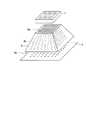
図1は、本発明の一実施形態に係る超音波用探触子を示す一部断面斜視図である。この超音波用探触子は、生体を被検体とする超音波診断装置において用いられるものであり、ケーブル7を介して超音波診断装置の本体と接続されている。また、この超音波用探触子は、超音波トランスデューサアレイ1と、配線体2と、FPC(Flexible Printed Circuit)インターポーザ3と、音響整合層4と、音響レンズ5とを含んでいる。これらの各部1〜5は筐体6に収納されている。
【0012】
超音波トランスデューサアレイ1は、圧電素子及びその両端に設けられる電極によって構成される複数の超音波トランスデューサを2次元に配列したものである。即ち、超音波トランスデューサアレイ1は、複数の圧電素子11と、共通電極12と、複数の電極13とを含んでいる。圧電素子11は、PZT(チタン酸ジルコン酸鉛:Pb(lead) zirconate titanate)に代表される圧電セラミックや、PVDF(polyvinyl difluoride:ポリフッ化ビニリデン)に代表される高分子圧電材料等によって形成されている。
【0013】
複数の圧電素子11の上底面は、例えば、金属等の導電体によって形成された共通電極12によって覆われている。共通電極12は、リード線を介して超音波診断装置の本体に接続され、そこで接地電位に接続されている。また、複数の圧電素子11の下底面には、金属等の導電体によって形成された電極13がそれぞれ設けられている。電極13は、後述する配線体等を介して、超音波診断装置の本体に含まれる電子回路に接続されている。なお、複数の圧電素子11の間にエポキシ樹脂系の接着剤等の絶縁材料14を充填することにより、これらの圧電素子11を固定及び保護しても良い。
【0014】
圧電素子11に、電極13及び共通電極12を介して電圧を印加することにより、圧電素子11は、圧電効果によって収縮して超音波を発生する。その際に、電極13に接続されている電子回路を用いて複数の圧電素子11を所定のタイミングで選択的に駆動することにより、所望の方向に送信される超音波ビームを形成することができる。また、圧電素子11は、超音波を受信することによって伸縮し、電気信号を発生する。
【0015】
超音波トランスデューサアレイ1の電極13側には、配線体2が設けられている。配線体2は、超音波トランスデューサアレイ1から配線を引き出すと共に、これらの超音波トランスデューサから発生した超音波を減衰させるバッキング層として働く。
【0016】
配線体2は、2次元に配列された複数の金属線21を、それらの金属線の間及び周囲に吸音材22を充填することによって固定したものである。金属線21は、直径が50μm〜300μm程度の細線であり、本実施形態においては、直径が100μmの細線が用いられている。これらの金属線21は、超音波トランスデューサアレイ1に含まれる複数の超音波トランスデューサの配列ピッチに合わせて配列されている。また、吸音材22は、エポキシ等の樹脂系接着剤に、PZTやセラミックのように音響減衰の大きい材料の粉体を混入して硬化させた絶縁材料である。
【0017】
このような配線体2は、複数の金属線21の断面が複数の電極13にそれぞれ対応するように、位置を合わせて配置されている。超音波トランスデューサ1と配線体1との接続部分においては、複数の金属線21と複数の電極13とが、導電性接着剤や半田等を用いてそれぞれ電気的に接続されていると共に、配線体2の吸音材22が、複数の超音波トランスデューサに直接、或いは、接着剤等を介して接続されている。このような配線体2を設けることにより、2次元マトリクスの内側に配置された超音波トランスデューサから配線が引き出されると共に、超音波トランスデューサアレイ1の後方(超音波の送信面の反対側)に向けて発生した超音波が吸収され、不要な超音波が減衰される。
【0018】
FPCインターポーザ3は、配線体2を介して超音波トランスデューサアレイ1と接続されている。ここで、FPC(フレキシブル基板)とは、絶縁性及び可撓性を有するベースフィルムの表面に、導電性の材料を用いて配線パターンを形成し、配線パターンを保護するためのカバーフィルムを設けたものである。
【0019】
FPCインターポーザ3には、所定のパターンで複数の信号線が形成されている。これらの信号線の一端には、配線体2の複数の金属線21の配列に対応して、複数の電極が形成されている。また、これらの信号線の他端は、ケーブル7に含まれる複数のリード線にそれぞれ接続されている。
【0020】
超音波トランスデューサ1の超音波送信面側には、音響整合層4が設けられている。音響整合層4は、超音波トランスデューサアレイ1の前方(超音波の送信面側)に配置されており、生体である被検体と超音波トランスデューサとの間の音響インピーダンスの不整合を解消する。これにより、超音波トランスデューサから送信された超音波が、効率良く被検体中に伝播する。音響整合層3の材料としては、例えば、パイレックス(登録商標)ガラスや金属等の粉体をエポキシ等の樹脂系材料中に分散させ、硬化させたものが用いられる。
【0021】
さらに、音響整合層4には、シリコンゴム等の音響レンズ5が設けられている。音響レンズ5は、超音波トランスデューサアレイから送信され、音響整合層4において音響インピーダンスを整合された超音波ビームを、所定の深度において集束させる。
【0022】
なお、本実施形態においては、図1に示すように、複数の超音波トランスデューサ1を2次元マトリクス状に配列しているが、この他にも、同心円状やランダム配置のように、様々な形態で配置することができる。その際には、複数の超音波トランスデューサの配列に合わせて、配線体2における金属線21の配列を変更する。
【0023】
また、図1に示す配線体2においては、複数の金属線21が平行に配列されているが、これらの配列は平行でなくても良い。即ち、図2に示すように、配線体8の一方の底面8aにおける複数の金属線8cの断面が、超音波トランスデューサアレイ1の複数の電極13にそれぞれ対応し、配線体8の他方の断面8bにおける複数の金属線8cの断面が、FPCインターポーザ3の複数の電極にそれぞれ対応するように、複数の金属線8cが配列されていれば良い。図2に示すように、断面8aから断面8bに向けて広がるように金属線8cを配列する場合には、配線間隔を広げることができるので、多数の微細な素子が密に配列された超音波トランスデューサアレイを用いる場合に、後段の回路における配線の接続を容易に行うことができる。
【0024】
次に、本発明の一実施形態に係る超音波用探触子の製造方法について、図1〜図6を参照しながら説明する。図3は、本実施形態に係る超音波用探触子の製造方法を示すフローチャートである。また、図4〜図7は、本実施形態に係る超音波用探触子の製造方法を説明するための図である。
【0025】
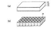
図3のステップS1において、図1に示す超音波トランスデューサアレイ1を作製する。図4は、超音波トランスデューサアレイ1の作製方法を説明するための図である。
図4の(a)に示すように、PZT板材32の一方の底面に、導電性接着剤等を用いて金属板31を接着し、PZT板材32の他方の底面に、スパッタリング等の成膜方法を用いて金属薄膜33を形成する。次いで、金属薄膜33及びPZT板材32を、ダイシング等の方法を用いてマトリクス状に分割する。これにより、図4の(b)に示すように、複数の電極をそれぞれ有する複数のPZT素子が共通電極上に2次元に配列された超音波トランスデューサアレイが作製される。さらに、複数のPZT素子の間に形成された溝34に絶縁材料を充填することにより、PZT素子を固定及び保護しても良い。
なお、ステップS1においては、その他の公知の方法を用いて超音波トランスデューサアレイ1を作製しても良い。
【0026】
次に、図3のステップS2において、図1に示す配線体2を作製する。図5は、配線体2の作製方法を説明するための図である。
図5の(a)に示すように、向かい合わせて配置された2つの固定板41の間に、超音波トランスデューサ1における素子の配列ピッチに合わせて金属線42を張る。次に、金属線42を張った2つの固定板41を容器に入れ、液状の吸音材を流し込んで硬化させる。ここで、液状の吸音材とは、例えば、エポキシ等の液状の樹脂系接着剤に、PZTやセラミックスの粉体を混合して分散させたものである。これにより、図5の(b)に示すように、金属線42の隙間や周囲に吸音材43が充填される。さらに、これを、I−I面及びII−II面において切断することにより、図5の(c)に示すように、金属線が2次元に配列された配線体2が作製される。なお、図5の(b)においては、金属線及び吸音材を2箇所において切断することによって1つの配線体を作製したが、これを2箇所以上において切断することにより、複数の配線体を作製しても良い。
【0027】
図3のステップS3において、超音波トランスデューサアレイ1と配線体2とを接続すると共に、配線体2とFPCインターポーザ3とを接続する。図6は、超音波トランスデューサアレイ1と配線体2との接続部分を示す断面図である。
図6の(a)に示すように、本実施形態においては、超音波トランスデューサアレイ1と配線体2とは、異方性導電接着剤(異方性導電ペースト)23を用いて接続している。ここで、異方性導電接着剤又は異方性導電ペースト(Anisotropic Conductive Paste:ACP)とは、液状の絶縁性接着剤の中に導電粒子を均一に分散させた固定材のことである。絶縁性接着剤としては、例えば、熱硬化性のエポキシ系樹脂が用いられ、導電粒子としては、例えば、金属粒子やプラスチック粒子の表面にニッケル(Ni)や金(Au)の薄膜を形成したものが用いられる。このような異方性導電接着剤23を、超音波トランスデューサアレイ1と配線体2との接着面に塗布し、加圧しながら加熱して固化させることにより、絶縁性接着剤中に分散している導電粒子が、電極13と金属線21との間に捕捉される。これにより、両者の接着面において、Z方向については導通が確保され、X方向及びY方向については絶縁性が示されるので、複数の電極13と複数の金属線21とが、それぞれ電気的に接続される。
【0028】
或いは、図6の(b)に示すように、複数の電極13と複数の金属線21とを、半田24や通常の導電性接着剤を用いてそれぞれ接続しても良い。
同様にして、配線体2とFPCインターポーザ3とを、異方性導電接着剤、半田、又は、通常の導電性接着剤を用いて接続する。
【0029】
ここで、超音波トランスデューサアレイ1と配線体2との位置関係、及び、配線体2とFPCインターポーザ3との位置関係は、精密にアライメントされる必要がある。そのためには、例えば、図7の(a)に示すように、超音波トランスデューサアレイ1と、配線体2と、FPCインターポーザ3とに、合わせマーク1a、2a、3aをそれぞれ設け、合わせマーク1a、2a、3aを基準として位置関係をアライメントすれば良い。或いは、図7の(b)に示すように、超音波トランスデューサアレイ1及びFPCインターポーザ3に、窓部1b及び3bをそれぞれ設け、配線体2に目印となるダミー金属線2bを配置し、窓部1b及び3bからダミーの金属線2bを覗くことにより、アライメントを行っても良い。
【0030】
図3のステップS4において、超音波トランスデューサ1の超音波送信面側に音響整合層4及び音響レンズ5を配置する。即ち、まず、ガラスや金属等の粉体をエポキシ等の樹脂系材料に分散させた音響整合用の部材を、樹脂系接着剤を用いて、超音波トランスデューサ1の共通電極12に接着する。次いで、シリコンゴム等の音響レンズ部材を、樹脂系接着剤を用いて、音響整合層4に接着する。
このようにして作製された超音波トランスデューサアレイ1〜音響整合層5を筐体6に収納することにより、図1に示す超音波用探触子が作製される。
【0031】
以上説明したように、本実施形態によれば、様々な配線ピッチに対応できると共に、配線ピッチのズレや断面のバラツキの少ない配線体を、容易に低コストで作製することができる。このような配線体を用いることにより、超音波トランスデューサアレイとFPCインターポーザとを、2次元的に容易且つ確実に接続することが可能になる。また、超音波トランスデューサアレイの後方に吸音材が配置されるので、後方に向けて発生した不要な超音波を効率的に減衰させて、ノイズを低減することが可能になる。
【0032】
次に、本実施形態に係る超音波用探触子の変形例について説明する。
本実施形態においては、異方性導電接着剤や半田等を用いて、配線体に含まれる金属線と、超音波トランスデューサアレイ又はFPCインターポーザの電極とを接続した。しかしながら、配線体の金属線にコネクタを設け、コネクタを介して配線体と超音波トランスデューサアレイ又はFPCインターポーザとを接続するようにしても良い。
【0033】
また、図8に示すように、超音波トランスデューサアレイの替わりに1−3コンポジット(複合圧電材料)9を用い、FPCインターポーザ2を介して1−3コンポジット9と配線体2とを接続しても良い。ここで、1−3コンポジットとは、樹脂材の中に複数の柱状の圧電材料を配置した複合構造体のことである。即ち、FPCインターポーザ2に含まれる複数の信号線の一端を、1−3コンポジット9に含まれる複数の圧電材料9aにそれぞれ接続すると共に、複数の信号線の他端を、配線体2に含まれる複数の金属線21に接続する。この場合には、FPCインターポーザ3によって、1−3コンポジット9に含まれる各々の圧電材料からの引き出し配線が広げられるので、配線体2及び後段の回路において、配線の接続を容易に行うことができる。
【0034】
或いは、図9に示すように、金属線25の端部が剥き出しになるように、吸音材26から金属線25を突出させても良い。金属線25を突出させることにより、金属線と超音波トランスデューサアレイ又はFPCインターポーザの電極との接触部分を増やすことができるので、より確実にコンタクトすることが可能になる。
【0035】
このような配線体は、例えば、次のように作製することができる。図5の(a)〜(c)に示すように、断面が平坦な配線体を作製した後で、断面にアセトン等の有機溶剤を塗布する。これにより、吸音材が解けて金属線が剥き出しになる。金属線を突出させる長さは、塗布する有機溶剤の量や浸透させる深さを調整することによって変更することができる。また、金属線を突出させた後で、金属線の長さを調節したり、金属線の断面の処理をしても良い。
【0036】
次に、本実施形態に係る超音波用探触子において用いられる配線体の別の作製方法について、図10〜図12を参照しながら説明する。図10は、配線体の別の作製方法を示すフローチャートであり、図11及び図12は、配線体の別の作製方法を説明するための図である。
【0037】
図10のステップS11において、吸音材によって被覆された金属線を作製する。例えば、図11の(a)に示すように、超音波トランスデューサの配列ピッチと等しい直径d又は1辺の長さを有する型81を用意し、そこに1本の金属線82を配置し、液状の吸音材83を注いで硬化させる。これにより、型の形状に合った吸音材84によって被覆された金属線が得られる。或いは、図11の(b)に示すように、1つの型に複数の金属線91を配置し、液状の吸音材を注いで硬化させることにより、被覆金属線の連続体92する。この連続体92を、複数の金属線91がそれぞれ分離されるように切断する。その際に、吸音材93の一辺の長さaが、超音波トランスデューサアレイ1における超音波トランスデューサの配列ピッチと等しくなるように成形する。これに、吸音材93によって被覆された金属線が得られる。
【0038】
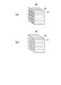
次に、ステップS12において、ステップS11において作製された吸音材によって被覆された金属線を複数束ね、接着剤を用いて接着する。これにより、図12の(a)に示す配線体80や、図12の(b)に示す配線体90が得られる。
【0039】
【発明の効果】
以上述べたように、本発明によれば、吸音材に複数の金属線を配置した配線体を用いるので、超音波トランスデューサが2次元に配列された超音波トランスデューサアレイであっても容易に配線を行うことができる。また、配線体に含まれる吸音材によって、超音波トランスデューサアレイの後方に向けて発生した超音波が吸収されるので、不要な超音波を効率的に減衰させてノイズを低減することが可能になる。
【図面の簡単な説明】
【図1】本発明の一実施形態に係る超音波トランスデューサの構造を示す断面斜視図である。
【図2】図1に示す配線体の変形例を示す図である。
【図3】本発明の一実施形態に係る超音波用探触子の製造方法を示すフローチャートである。
【図4】超音波トランスデューサアレイの作製方法を説明するための図である。
【図5】配線体の作製方法を説明するための図である。
【図6】超音波トランスデューサアレイと配線体との接続部分を示す断面図である。
【図7】超音波トランスデューサアレイと、配線体と、FPCインターポーザとをアライメントする方法を説明するための図である。
【図8】本発明の一実施形態に係る超音波用探触子の変形例を示す図である。
【図9】配線体の変形例を示す図である。
【図10】配線体の別の作製方法を示すフローチャートである。
【図11】配線体の別の作製方法を説明するための図である。
【図12】図10に示す方法を用いて作製された配線体を示す斜視図である。
【符号の説明】
1 超音波トランスデューサアレイ
1a〜3a 合わせマーク
1b、3b 窓部
2b ダミー金属線
2、8、80、90 配線体
3 FPCインターポーザ
4 音響整合層
5 音響レンズ
6 筐体
7 ケーブル
9 1−3コンポジット
11 圧電素子
12 共通電極
13 電極
14 絶縁材料
21、25、42、82、91 金属線
22、26、43、84、93 吸音材
23 異方性導電接着剤
24 半田
31 金属板
32 PZT板材
33 金属薄膜
34 溝
41 固定板
81 型
83 液状の吸音材
92 被覆金属線の連続体[0001]
BACKGROUND OF THE INVENTION
The present invention relates to an ultrasonic probe used in an ultrasonic diagnostic apparatus for medical use or nondestructive inspection, and a manufacturing method thereof, and more particularly, to an ultrasonic probe including a two-dimensional sensor array and a manufacturing method thereof. .
[0002]
[Prior art]
In general, as an element (ultrasonic transducer) used for transmission and reception of ultrasonic waves, piezoelectric ceramics represented by PZT (lead zirconate titanate: Pb (lead) zirconate titanate), PVDF (polyvinylidene fluoride: polyfluoridyl fluoride) Piezoelectric elements including polymer piezoelectric elements represented by (1) are used. When electrodes are formed at both ends of such a piezoelectric element and a voltage is applied to the piezoelectric element via the electrode, the piezoelectric element expands and contracts due to the piezoelectric effect, and ultrasonic waves are generated. Therefore, when a large number of piezoelectric elements are arranged and these piezoelectric elements are driven with a predetermined time difference, an ultrasonic beam having a focal point at a desired depth is transmitted by synthesis of ultrasonic waves generated from the respective piezoelectric elements. The
[0003]
In recent years, in order to acquire a three-dimensional image in real time, development of a two-dimensional sensor array capable of acquiring cross-sectional images at a plurality of positions without mechanically moving the subject when scanning the subject has been advanced. . However, in order to put an ultrasonic probe having a two-dimensional sensor array into practical use, these elements must be highly integrated. For this purpose, microfabrication of elements and wiring to each element are required, but it is difficult to route wiring to a large number of two-dimensionally arranged microelements, and methods for solving these problems have been studied. Yes.
[0004]
For example, in
[0005]
However, in such a wiring method, the wiring pitch tends to shift due to variations in film thickness and adhesive thickness. Further, when the base film on which the signal wiring is formed is cut and the cross section thereof is connected to the element, the signal wiring and the element may not be reliably connected due to unevenness of the cut surface. For this reason, the yield in the wiring or bonding process is deteriorated.
[0006]
[Patent Document 1]
JP 2000-214144 A (first page, FIG. 1)
[0007]
[Problems to be solved by the invention]
Therefore, in view of the above points, an object of the present invention is to perform wiring easily and reliably in an ultrasonic probe including a plurality of ultrasonic transducers arranged two-dimensionally.
[0008]
[Means for Solving the Problems]
In order to solve the above problems, an ultrasonic probe according to the present invention includes an ultrasonic transducer array in which a plurality of piezoelectric elements provided with electrodes are two-dimensionally arranged, and a cross section of the plurality of piezoelectric elements. A plurality of metal wires electrically connected to the electrodes provided on the plurality of piezoelectric elements, and a sound absorbing material filled between the plurality of metal wires. Including a wiring body.
[0009]
The ultrasonic probe manufacturing method according to the present invention includes a step (a) of preparing an ultrasonic transducer array by two-dimensionally arranging a plurality of piezoelectric elements provided with electrodes, and a cross section thereof. Preparing a wiring body including a plurality of metal wires arranged so as to correspond to the arrangement of the plurality of piezoelectric elements, and a sound absorbing material filled between the plurality of metal wires; (C) electrically connecting a plurality of electrodes included in the acoustic transducer array and one end of a plurality of metal wires included in the wiring body to the electrodes.
[0010]
According to the present invention, since the wiring body in which the sound absorbing material is filled between the plurality of metal wires is used, the wiring can be easily and reliably pulled out from the ultrasonic transducer array.
[0011]
DETAILED DESCRIPTION OF THE INVENTION
Hereinafter, embodiments of the present invention will be described in detail with reference to the drawings. The same constituent elements are denoted by the same reference numerals, and the description thereof is omitted.
FIG. 1 is a partial cross-sectional perspective view showing an ultrasonic probe according to an embodiment of the present invention. This ultrasonic probe is used in an ultrasonic diagnostic apparatus that uses a living body as a subject, and is connected to the main body of the ultrasonic diagnostic apparatus via a cable 7. The ultrasonic probe includes an
[0012]
The
[0013]
The upper and lower surfaces of the plurality of
[0014]
By applying a voltage to the
[0015]
A
[0016]
The
[0017]
Such a
[0018]
The
[0019]
In the
[0020]
An
[0021]
Furthermore, the
[0022]
In the present embodiment, as shown in FIG. 1, a plurality of
[0023]
In the
[0024]
Next, a method for manufacturing an ultrasonic probe according to an embodiment of the present invention will be described with reference to FIGS. FIG. 3 is a flowchart showing a method for manufacturing the ultrasonic probe according to the present embodiment. 4 to 7 are views for explaining a method of manufacturing the ultrasonic probe according to the present embodiment.
[0025]
In step S1 of FIG. 3, the
As shown in FIG. 4A, a metal plate 31 is bonded to one bottom surface of the PZT plate material 32 using a conductive adhesive or the like, and a film forming method such as sputtering is applied to the other bottom surface of the PZT plate material 32. The metal
In step S1, the
[0026]
Next, in step S2 of FIG. 3, the
As shown in FIG. 5A, a
[0027]
In step S3 of FIG. 3, the
As shown in FIG. 6A, in the present embodiment, the
[0028]
Alternatively, as shown in FIG. 6B, a plurality of
Similarly, the
[0029]
Here, the positional relationship between the
[0030]
In step S <b> 4 of FIG. 3, the
By housing the
[0031]
As described above, according to the present embodiment, it is possible to easily produce a wiring body that can cope with various wiring pitches and that has little wiring pitch deviation and cross-sectional variation. By using such a wiring body, the ultrasonic transducer array and the FPC interposer can be easily and reliably connected in two dimensions. In addition, since the sound absorbing material is disposed behind the ultrasonic transducer array, it is possible to efficiently attenuate unnecessary ultrasonic waves generated toward the rear and reduce noise.
[0032]
Next, a modified example of the ultrasonic probe according to the present embodiment will be described.
In the present embodiment, the metal wires included in the wiring body and the electrodes of the ultrasonic transducer array or the FPC interposer are connected using an anisotropic conductive adhesive or solder. However, a connector may be provided on the metal wire of the wiring body, and the wiring body and the ultrasonic transducer array or the FPC interposer may be connected via the connector.
[0033]
Further, as shown in FIG. 8, a 1-3 composite (composite piezoelectric material) 9 is used instead of the ultrasonic transducer array, and the 1-3 composite 9 and the
[0034]
Alternatively, as shown in FIG. 9, the
[0035]
Such a wiring body can be manufactured as follows, for example. As shown in FIGS. 5A to 5C, after producing a wiring body having a flat cross section, an organic solvent such as acetone is applied to the cross section. As a result, the sound absorbing material is unwound and the metal wire is exposed. The length by which the metal wire is projected can be changed by adjusting the amount of the organic solvent to be applied and the penetration depth. Further, after the metal wire is protruded, the length of the metal wire may be adjusted or the cross section of the metal wire may be processed.
[0036]
Next, another method for producing a wiring body used in the ultrasonic probe according to the present embodiment will be described with reference to FIGS. FIG. 10 is a flowchart showing another method for manufacturing a wiring body, and FIGS. 11 and 12 are diagrams for explaining another method for manufacturing the wiring body.
[0037]
In step S11 of FIG. 10, a metal wire covered with a sound absorbing material is produced. For example, as shown in FIG. 11 (a), a
[0038]
Next, in step S12, a plurality of metal wires covered with the sound absorbing material produced in step S11 are bundled and bonded using an adhesive. Thereby, the
[0039]
【The invention's effect】
As described above, according to the present invention, since a wiring body in which a plurality of metal wires are arranged on a sound absorbing material is used, wiring can be easily performed even in an ultrasonic transducer array in which ultrasonic transducers are two-dimensionally arranged. It can be carried out. In addition, since the ultrasonic wave generated toward the rear of the ultrasonic transducer array is absorbed by the sound absorbing material included in the wiring body, it is possible to efficiently attenuate unnecessary ultrasonic waves and reduce noise. .
[Brief description of the drawings]
FIG. 1 is a cross-sectional perspective view showing the structure of an ultrasonic transducer according to an embodiment of the present invention.
FIG. 2 is a view showing a modification of the wiring body shown in FIG.
FIG. 3 is a flowchart showing a method for manufacturing an ultrasonic probe according to an embodiment of the present invention.
FIG. 4 is a diagram for explaining a method of manufacturing an ultrasonic transducer array.
FIG. 5 is a diagram for explaining a method for manufacturing a wiring body;
FIG. 6 is a cross-sectional view showing a connection portion between an ultrasonic transducer array and a wiring body.
FIG. 7 is a diagram for explaining a method of aligning an ultrasonic transducer array, a wiring body, and an FPC interposer.
FIG. 8 is a view showing a modification of the ultrasonic probe according to the embodiment of the present invention.
FIG. 9 is a view showing a modified example of a wiring body.
FIG. 10 is a flowchart showing another method for manufacturing a wiring body;
FIG. 11 is a diagram for explaining another method for manufacturing a wiring body;
12 is a perspective view showing a wiring body manufactured using the method shown in FIG.
[Explanation of symbols]
DESCRIPTION OF
Claims (8)
Translated fromJapanese断面が前記複数の圧電素子の配列に対応するように配置されると共に、前記複数の圧電素子に設けられた電極とそれぞれ電気的に接続された複数の金属線と、前記複数の金属線の間に充填された吸音材とを含む配線体と、
を具備する超音波用探触子。An ultrasonic transducer array in which a plurality of piezoelectric elements provided with electrodes are two-dimensionally arranged;
Between the plurality of metal wires and a plurality of metal wires that are arranged so that a cross section corresponds to the arrangement of the plurality of piezoelectric elements, and are electrically connected to electrodes provided in the plurality of piezoelectric elements, respectively. A wiring body including a sound absorbing material filled in,
An ultrasonic probe comprising:
断面が前記複数の圧電素子の配列に対応するように配置された複数の金属線と、前記複数の金属線の間に充填された吸音材とを含む配線体を用意するステップ(b)と、
前記超音波トランスデューサアレイに含まれる複数の電極と、前記配線体に含まれる複数の金属線の一端とを、電極と電気的に接続するステップ(c)と、
を具備する超音波用探触子の製造方法。A step (a) of preparing an ultrasonic transducer array by two-dimensionally arranging a plurality of piezoelectric elements provided with electrodes;
Preparing a wiring body including a plurality of metal wires arranged so that a cross section thereof corresponds to the arrangement of the plurality of piezoelectric elements, and a sound absorbing material filled between the plurality of metal wires;
Electrically connecting a plurality of electrodes included in the ultrasonic transducer array and one end of a plurality of metal wires included in the wiring body to the electrodes;
A method for manufacturing an ultrasonic probe comprising:
所定の間隔で向かい合うように配置された所定の面積を有する2つの板に、断面が前記複数の圧電素子の配列に対応するように金属線を張る工程と、
前記2つの板の間に液状の吸音材を流し込んで硬化させることにより、前記金属線の間を吸音材で充填する工程と、
前記金属線及び前記吸音材を、金属線と交わる面で切断する工程と、
を含む、請求項7記載の超音波用探触子の製造方法。Step (b) is for producing the wiring body.
Stretching a metal wire on two plates having a predetermined area arranged to face each other at a predetermined interval so that a cross section corresponds to the arrangement of the plurality of piezoelectric elements;
Filling a space between the metal wires with a sound absorbing material by pouring and curing a liquid sound absorbing material between the two plates;
Cutting the metal wire and the sound absorbing material at a surface intersecting the metal wire;
The manufacturing method of the probe for ultrasonic waves of Claim 7 containing this.
Priority Applications (1)
| Application Number | Priority Date | Filing Date | Title |
|---|---|---|---|
| JP2003157581AJP2004363746A (en) | 2003-06-03 | 2003-06-03 | Ultrasonic probe and its manufacturing method |
Applications Claiming Priority (1)
| Application Number | Priority Date | Filing Date | Title |
|---|---|---|---|
| JP2003157581AJP2004363746A (en) | 2003-06-03 | 2003-06-03 | Ultrasonic probe and its manufacturing method |
Publications (1)
| Publication Number | Publication Date |
|---|---|
| JP2004363746Atrue JP2004363746A (en) | 2004-12-24 |
Family
ID=34051244
Family Applications (1)
| Application Number | Title | Priority Date | Filing Date |
|---|---|---|---|
| JP2003157581APendingJP2004363746A (en) | 2003-06-03 | 2003-06-03 | Ultrasonic probe and its manufacturing method |
Country Status (1)
| Country | Link |
|---|---|
| JP (1) | JP2004363746A (en) |
Cited By (16)
| Publication number | Priority date | Publication date | Assignee | Title |
|---|---|---|---|---|
| JP2007130385A (en)* | 2005-11-14 | 2007-05-31 | Aloka Co Ltd | Ultrasonic probe and backing for use in the same |
| JP2008545501A (en)* | 2005-06-07 | 2008-12-18 | コーニンクレッカ フィリップス エレクトロニクス エヌ ヴィ | Backing block for ultrasonic sensor assembly |
| JP2009060501A (en)* | 2007-09-03 | 2009-03-19 | Fujifilm Corp | Backing material, ultrasonic probe, ultrasonic endoscope, ultrasonic diagnostic apparatus, and ultrasonic endoscope apparatus |
| JP2010124467A (en)* | 2008-11-19 | 2010-06-03 | Medison Co Ltd | Probe for ultrasonic diagnostic equipment and method of manufacturing the same |
| KR101080576B1 (en) | 2007-11-22 | 2011-11-04 | 도시바 메디칼 시스템즈 코포레이션 | Ultrasonic probe, ultrasonic diagnosis apparatus, and ultrasonic probe manufacturing method |
| JP5282305B2 (en)* | 2007-05-10 | 2013-09-04 | コニカミノルタ株式会社 | Ultrasonic probe and ultrasonic diagnostic apparatus |
| JP5348250B2 (en)* | 2009-11-30 | 2013-11-20 | コニカミノルタ株式会社 | Acoustic braking component for ultrasonic probe, ultrasonic probe, and method of manufacturing ultrasonic probe |
| JP2013243668A (en)* | 2012-05-22 | 2013-12-05 | General Electric Co <Ge> | Ultrasound transducer and method for manufacturing ultrasound transducer |
| WO2014091970A1 (en)* | 2012-12-12 | 2014-06-19 | オリンパス株式会社 | Connection structure for semiconductor device, ultrasonic module, and ultrasonic endoscope system having built-in ultrasonic module |
| JP2015033571A (en)* | 2013-07-10 | 2015-02-19 | コニカミノルタ株式会社 | Phasing adder and ultrasonic probe |
| JP2017500804A (en)* | 2013-12-11 | 2017-01-05 | フジフィルム ディマティックス, インコーポレイテッド | Flexible micro-machined transducer device and manufacturing method thereof |
| JP2017109072A (en)* | 2015-12-11 | 2017-06-22 | 東芝メディカルシステムズ株式会社 | Ultrasonic probe |
| WO2017169374A1 (en)* | 2016-04-01 | 2017-10-05 | 富士フイルム株式会社 | Ultrasonic oscillator unit and ultrasonic endoscope using same |
| JP2019016934A (en)* | 2017-07-07 | 2019-01-31 | コニカミノルタ株式会社 | MEMS transducer manufacturing method, MEMS transducer, ultrasonic probe, and ultrasonic diagnostic apparatus |
| WO2019088146A1 (en)* | 2017-11-01 | 2019-05-09 | 富士フイルム株式会社 | Resin composition for acoustic matching layer, cured product, acoustic matching sheet, acoustic wave probe, acoustic wave measurement device, production method for acoustic wave probe, and material set for acoustic matching layer |
| JP2021526324A (en)* | 2018-05-03 | 2021-09-30 | フジフィルム ソノサイト インコーポレイテッド | Dual frequency ultrasonic transducer |
Citations (3)
| Publication number | Priority date | Publication date | Assignee | Title |
|---|---|---|---|---|
| JP2000166923A (en)* | 1998-12-09 | 2000-06-20 | Toshiba Corp | Ultrasonic transducer and method of manufacturing the same |
| JP2002095090A (en)* | 2000-09-14 | 2002-03-29 | Aloka Co Ltd | Ultrasonic probe and its manufacturing method |
| JP2002345094A (en)* | 2001-05-22 | 2002-11-29 | Aloka Co Ltd | Backing for ultrasonic wave probe and its manufacturing method |
- 2003
- 2003-06-03JPJP2003157581Apatent/JP2004363746A/enactivePending
Patent Citations (3)
| Publication number | Priority date | Publication date | Assignee | Title |
|---|---|---|---|---|
| JP2000166923A (en)* | 1998-12-09 | 2000-06-20 | Toshiba Corp | Ultrasonic transducer and method of manufacturing the same |
| JP2002095090A (en)* | 2000-09-14 | 2002-03-29 | Aloka Co Ltd | Ultrasonic probe and its manufacturing method |
| JP2002345094A (en)* | 2001-05-22 | 2002-11-29 | Aloka Co Ltd | Backing for ultrasonic wave probe and its manufacturing method |
Cited By (26)
| Publication number | Priority date | Publication date | Assignee | Title |
|---|---|---|---|---|
| JP2008545501A (en)* | 2005-06-07 | 2008-12-18 | コーニンクレッカ フィリップス エレクトロニクス エヌ ヴィ | Backing block for ultrasonic sensor assembly |
| JP2007130385A (en)* | 2005-11-14 | 2007-05-31 | Aloka Co Ltd | Ultrasonic probe and backing for use in the same |
| JP5282305B2 (en)* | 2007-05-10 | 2013-09-04 | コニカミノルタ株式会社 | Ultrasonic probe and ultrasonic diagnostic apparatus |
| JP2009060501A (en)* | 2007-09-03 | 2009-03-19 | Fujifilm Corp | Backing material, ultrasonic probe, ultrasonic endoscope, ultrasonic diagnostic apparatus, and ultrasonic endoscope apparatus |
| KR101080576B1 (en) | 2007-11-22 | 2011-11-04 | 도시바 메디칼 시스템즈 코포레이션 | Ultrasonic probe, ultrasonic diagnosis apparatus, and ultrasonic probe manufacturing method |
| JP2010124467A (en)* | 2008-11-19 | 2010-06-03 | Medison Co Ltd | Probe for ultrasonic diagnostic equipment and method of manufacturing the same |
| JP5348250B2 (en)* | 2009-11-30 | 2013-11-20 | コニカミノルタ株式会社 | Acoustic braking component for ultrasonic probe, ultrasonic probe, and method of manufacturing ultrasonic probe |
| JP2013243668A (en)* | 2012-05-22 | 2013-12-05 | General Electric Co <Ge> | Ultrasound transducer and method for manufacturing ultrasound transducer |
| WO2014091970A1 (en)* | 2012-12-12 | 2014-06-19 | オリンパス株式会社 | Connection structure for semiconductor device, ultrasonic module, and ultrasonic endoscope system having built-in ultrasonic module |
| JP2014116904A (en)* | 2012-12-12 | 2014-06-26 | Olympus Corp | Semiconductor device connection structure, ultrasonic module, and ultrasonic endoscope system mounting ultrasonic module |
| US9997449B2 (en) | 2012-12-12 | 2018-06-12 | Olympus Corporation | Semiconductor device connection structure, ultrasonic module, and ultrasonic endoscope system having ultrasonic module |
| JP2015033571A (en)* | 2013-07-10 | 2015-02-19 | コニカミノルタ株式会社 | Phasing adder and ultrasonic probe |
| JP2017500804A (en)* | 2013-12-11 | 2017-01-05 | フジフィルム ディマティックス, インコーポレイテッド | Flexible micro-machined transducer device and manufacturing method thereof |
| JP2017109072A (en)* | 2015-12-11 | 2017-06-22 | 東芝メディカルシステムズ株式会社 | Ultrasonic probe |
| WO2017169374A1 (en)* | 2016-04-01 | 2017-10-05 | 富士フイルム株式会社 | Ultrasonic oscillator unit and ultrasonic endoscope using same |
| JPWO2017169374A1 (en)* | 2016-04-01 | 2019-01-17 | 富士フイルム株式会社 | Ultrasonic transducer unit and ultrasonic endoscope using the same |
| US11730450B2 (en) | 2016-04-01 | 2023-08-22 | Fujifilm Corporation | Ultrasonic oscillator unit and ultrasonic endoscope using same |
| JP2019016934A (en)* | 2017-07-07 | 2019-01-31 | コニカミノルタ株式会社 | MEMS transducer manufacturing method, MEMS transducer, ultrasonic probe, and ultrasonic diagnostic apparatus |
| JP6992292B2 (en) | 2017-07-07 | 2022-01-13 | コニカミノルタ株式会社 | Manufacturing method of MEMS transducer, MEMS transducer, ultrasonic probe, and ultrasonic diagnostic equipment |
| US11369345B2 (en) | 2017-07-07 | 2022-06-28 | Konica Minolta, Inc. | Method for producing MEMS transducer, MEMS transducer, ultrasound probe, and ultrasound diagnostic apparatus |
| WO2019088146A1 (en)* | 2017-11-01 | 2019-05-09 | 富士フイルム株式会社 | Resin composition for acoustic matching layer, cured product, acoustic matching sheet, acoustic wave probe, acoustic wave measurement device, production method for acoustic wave probe, and material set for acoustic matching layer |
| JPWO2019088146A1 (en)* | 2017-11-01 | 2020-11-19 | 富士フイルム株式会社 | Resin composition for acoustic matching layer, cured product, acoustic matching sheet, acoustic wave probe, acoustic wave measuring device, manufacturing method of acoustic wave probe, and material set for acoustic matching layer |
| US11572467B2 (en) | 2017-11-01 | 2023-02-07 | Fujifilm Corporation | Resin composition for acoustic matching layer, cured product, acoustic matching sheet, acoustic probe, acoustic measuring apparatus, method for producing acoustic probe, and acoustic matching layer material set |
| JP2021526324A (en)* | 2018-05-03 | 2021-09-30 | フジフィルム ソノサイト インコーポレイテッド | Dual frequency ultrasonic transducer |
| US11774589B2 (en) | 2018-05-03 | 2023-10-03 | Fujifilm Sonosite, Inc. | Dual frequency ultrasound transducer |
| JP7362659B2 (en) | 2018-05-03 | 2023-10-17 | フジフィルム ソノサイト インコーポレイテッド | dual frequency ultrasound transducer |
Similar Documents
| Publication | Publication Date | Title |
|---|---|---|
| US6936008B2 (en) | Ultrasound system with cableless coupling assembly | |
| US7530151B2 (en) | Vibrator array, manufacturing method thereof, and ultrasonic probe | |
| JP2004363746A (en) | Ultrasonic probe and its manufacturing method | |
| US7288069B2 (en) | Ultrasonic probe and method of manufacturing the same | |
| US6640634B2 (en) | Ultrasonic probe, method of manufacturing the same and ultrasonic diagnosis apparatus | |
| US9263663B2 (en) | Method of making thick film transducer arrays | |
| US20110237952A1 (en) | Two-dimensional-array ultrasonic probe and ultrasonic diagnostic apparatus | |
| EP2459322B1 (en) | Ultrasound imaging transducer acoustic stack with integral electrical connections | |
| JP2009255036A (en) | Ultrasonic probe and its manufacturing method | |
| JP2001309493A (en) | Two-dimensional array ultrasonic probe and method of manufacturing the same | |
| CN103518385A (en) | Ultrasonic transducer, ultrasonic probe, and manufacturing method of ultrasonic transducer | |
| CN101402086A (en) | Ultrasonic probe and piezoelectric transducer | |
| JPH0723500A (en) | Two-dimensional array ultrasonic probe | |
| JPS5920240B2 (en) | Ultrasonic probe and method for manufacturing the ultrasonic probe | |
| JP4261298B2 (en) | LAMINATED STRUCTURE ARRAY, ITS MANUFACTURING METHOD, AND ULTRASONIC TRANSDUCER ARRAY | |
| JP4516451B2 (en) | Ultrasonic probe and method for producing ultrasonic probe | |
| JP4426513B2 (en) | Ultrasonic probe and manufacturing method thereof | |
| JP2005117159A (en) | Ultrasonic transducer array and manufacturing method therefor | |
| JPH05123317A (en) | Two-dimensional array ultrasonic probe | |
| JP4071084B2 (en) | Manufacturing method of two-dimensional array ultrasonic probe | |
| JP2000214144A (en) | Two-dimensional array ultrasonic probe | |
| KR102359155B1 (en) | Hybrid ultrasound prove array and method of manufacturing the same | |
| JP5228924B2 (en) | Vibration element, ultrasonic device using the vibration element, and method for manufacturing vibration element | |
| JP2000125393A (en) | Ultrasonic wave transducer | |
| JPH0532059B2 (en) |
Legal Events
| Date | Code | Title | Description |
|---|---|---|---|
| A621 | Written request for application examination | Free format text:JAPANESE INTERMEDIATE CODE: A621 Effective date:20060215 | |
| A711 | Notification of change in applicant | Free format text:JAPANESE INTERMEDIATE CODE: A712 Effective date:20061204 | |
| A977 | Report on retrieval | Free format text:JAPANESE INTERMEDIATE CODE: A971007 Effective date:20080407 | |
| A131 | Notification of reasons for refusal | Free format text:JAPANESE INTERMEDIATE CODE: A131 Effective date:20080415 | |
| A02 | Decision of refusal | Free format text:JAPANESE INTERMEDIATE CODE: A02 Effective date:20081007 |